CERAMICS INTERNATIONAL Available online at www.sciencedirect.com Ceramics International 41 (2015) 913–920 Nanocolumnar zinc oxide as a transparent conductive oxide film for a blue InGaN-based light emitting diode Nur Ameera a,n,1 , Ahmad Shuhaimi a,1 , Najwa Surani a,1 , Mohamad Rusop b,1 , Muhammad Hakim a,1 , Mohamad Hafiz Mamat b,1 , Mazwan Mansor a,1 , Mohd Sobri a,1 , V. Ganesh a,1 , Yusnizam Yusuf a,1 a Nitride Semiconductor Research Laboratory, Low Dimensional Materials Research Center, Department of Physics, Faculty of Sciences, University of Malaya 50603 Kuala Lumpur, Malaysia b NANO-Electronic Centre, Faculty of Electrical Engineering, Universiti Teknologi MARA (UiTM), 40450 Shah Alam, Selangor, Malaysia Received 16 June 2014; received in revised form 3 July 2014; accepted 2 September 2014 Available online 8 September 2014 Abstract A comprehensive study of ZnO nanocolumnar structure has been conducted through x-ray diffraction spectroscopy, atomic force microscopy, field emission scanning electron microscopy and UV-visible spectroscopy measurements. This study involves the development of an efficient ZnO transparent conductive oxide film fabricated by RF magnetron sputtering for use in a blue indium gallium nitride based light emitting diode. FESEM measurements revealed that a maximum growth temperature of 500 1C induced the formation of a nanocolumnar structure. The XRD measurements revealed that the stress reduction in the film also contributed to a superior ZnO nanocolumnar structure. In addition, the reduction of the oxygen percentage during deposition resulted in significant improvement of the structure. The reduced atomic peening effect yielded lower stress in the film. Thus, a dense, uniform-thickness, fine nanocolumnar ZnO of lateral size measuring 30 to 60 nm was successfully fabricated at the lowest oxygen percentage of 7%. This film also exhibited good transparency at the blue region with 78% optical transmission. & 2014 Elsevier Ltd and Techna Group S.r.l. All rights reserved. Keywords: Zinc oxide; Nanocolumnar; Transparent conductive oxide; RF magnetron sputtering 1. Introduction Transparent conductive oxide (TCO) film is predominantly used in optoelectronic devices, such as solar cells and light emitting diodes (LEDs). In both applications, TCO film is deposited on top of the device structure and functions as a window for light to pass; in LEDs, the light is from the active region. Also, the TCO film acts as an ohmic contact for carrier transport in the device. Therefore, the TCO should consist of material with a large bandgap, as well as high transparency and conductivity. Metal oxide materials, such as indium tin oxide (ITO) and zinc oxide (ZnO), are usually used as the TCO material. This paper describes the fabrication of nanostructured TCO film based on pure ZnO material. The work was designed to examine the deposition of pure ZnO as a TCO film on a blue indium gallium nitride (InGaN)-based LED. The TCO films were used to improve the light extraction efficiency (LEE) of the LED. Many researchers have attempted to obtain an InGaN-blue LED with optimal characteristics, including pro- ducing a high LEE via a surface roughening technique. The p-GaN layer can be textured by a maskless wet-etching process [1], while the use of either electron-beam [2] or nanoimprint [3] lithography can be used to promote a rougher LED surface. A rough surface will improve the amount of light that is scattered out from the LED, thus enhancing the LEE [4]. However, such methods exhibit low manufacturing yields and involve high cost, which are not suitable for the industrial. In our work, the nanostructured TCO film is deposited on top of the LED structure to produce a rough surface. We aimed for a film with nanocolumnar structure so that, in addition to a high surface to volume ratio, the columnar structure will also act as www.elsevier.com/locate/ceramint http://dx.doi.org/10.1016/j.ceramint.2014.09.009 0272-8842/& 2014 Elsevier Ltd and Techna Group S.r.l. All rights reserved. n Corresponding author. E-mail addresses: [email protected] (N. Ameera), [email protected] (A. Shuhaimi). 1 Tel.: þ03 7967 4206.

Welcome message from author
This document is posted to help you gain knowledge. Please leave a comment to let me know what you think about it! Share it to your friends and learn new things together.
Transcript
CERAMICSINTERNATIONAL
Available online at www.sciencedirect.com
http://dx.doi.org/0272-8842/& 20
nCorrespondinE-mail addre
[email protected].: þ03 79
1 (2015) 913–920
Ceramics International 4 www.elsevier.com/locate/ceramintNanocolumnar zinc oxide as a transparent conductive oxide film for a blueInGaN-based light emitting diode
Nur Ameeraa,n,1, Ahmad Shuhaimia,1, Najwa Surania,1, Mohamad Rusopb,1, Muhammad Hakima,1,Mohamad Hafiz Mamatb,1, Mazwan Mansora,1, Mohd Sobria,1, V. Ganesha,1, Yusnizam Yusufa,1
aNitride Semiconductor Research Laboratory, Low Dimensional Materials Research Center, Department of Physics, Faculty of Sciences, University of Malaya50603 Kuala Lumpur, Malaysia
bNANO-Electronic Centre, Faculty of Electrical Engineering, Universiti Teknologi MARA (UiTM), 40450 Shah Alam, Selangor, Malaysia
Received 16 June 2014; received in revised form 3 July 2014; accepted 2 September 2014Available online 8 September 2014
Abstract
A comprehensive study of ZnO nanocolumnar structure has been conducted through x-ray diffraction spectroscopy, atomic force microscopy,field emission scanning electron microscopy and UV-visible spectroscopy measurements. This study involves the development of an efficientZnO transparent conductive oxide film fabricated by RF magnetron sputtering for use in a blue indium gallium nitride based light emitting diode.FESEM measurements revealed that a maximum growth temperature of 500 1C induced the formation of a nanocolumnar structure. The XRDmeasurements revealed that the stress reduction in the film also contributed to a superior ZnO nanocolumnar structure. In addition, the reductionof the oxygen percentage during deposition resulted in significant improvement of the structure. The reduced atomic peening effect yielded lowerstress in the film. Thus, a dense, uniform-thickness, fine nanocolumnar ZnO of lateral size measuring 30 to 60 nm was successfully fabricated atthe lowest oxygen percentage of 7%. This film also exhibited good transparency at the blue region with 78% optical transmission.& 2014 Elsevier Ltd and Techna Group S.r.l. All rights reserved.
Keywords: Zinc oxide; Nanocolumnar; Transparent conductive oxide; RF magnetron sputtering
1. Introduction
Transparent conductive oxide (TCO) film is predominantlyused in optoelectronic devices, such as solar cells and lightemitting diodes (LEDs). In both applications, TCO film isdeposited on top of the device structure and functions as awindow for light to pass; in LEDs, the light is from the activeregion. Also, the TCO film acts as an ohmic contact for carriertransport in the device. Therefore, the TCO should consist ofmaterial with a large bandgap, as well as high transparency andconductivity. Metal oxide materials, such as indium tin oxide(ITO) and zinc oxide (ZnO), are usually used as the TCOmaterial. This paper describes the fabrication of nanostructured
10.1016/j.ceramint.2014.09.00914 Elsevier Ltd and Techna Group S.r.l. All rights reserved.
g author.sses: [email protected] (N. Ameera),du.my (A. Shuhaimi).67 4206.
TCO film based on pure ZnO material. The work was designedto examine the deposition of pure ZnO as a TCO film on a blueindium gallium nitride (InGaN)-based LED. The TCO filmswere used to improve the light extraction efficiency (LEE) ofthe LED. Many researchers have attempted to obtain anInGaN-blue LED with optimal characteristics, including pro-ducing a high LEE via a surface roughening technique. Thep-GaN layer can be textured by a maskless wet-etching process[1], while the use of either electron-beam [2] or nanoimprint[3] lithography can be used to promote a rougher LED surface.A rough surface will improve the amount of light that isscattered out from the LED, thus enhancing the LEE [4].However, such methods exhibit low manufacturing yields andinvolve high cost, which are not suitable for the industrial. Inour work, the nanostructured TCO film is deposited on top ofthe LED structure to produce a rough surface. We aimed for afilm with nanocolumnar structure so that, in addition to a highsurface to volume ratio, the columnar structure will also act as
(e) 400oC
(f) 500oCZnO(002)
ZnO(103)
N. Ameera et al. / Ceramics International 41 (2015) 913–920914
waveguides that function as an internal lens and a path for thelight to be emitted. Furthermore, the denser and finer nanoco-lumnar structure possessed by the film may be used to producea more efficient TCO.
Besides ITO, we worked on ZnO due its unique properties,including wide direct bandgap of 3.37 eV, strong bindingenergy of 60 meV, high transparency, efficient transmission inthe blue spectral region and the same wurtzite hexagonalstructure as GaN. The sputtering technique was chosen forthe growth method due to high probability of producing acolumnar structure, as reported by others [5,6]. In addition,sputtering is regarded as a relative simple and economicalapproach for scalable industrial production. The properties ofZnO are critically related to the growth parameters [7,8].Hence, in this study, ZnO films were deposited under severalconditions to observe their effects on its properties, andparticularly on its nanocolumnar structure. The goal of thisstudy is the improvement of ZnO as a TCO film for applicationin a blue InGaN LED because this application has been lessstudied by others. The ZnO film is grown on silicon (Si)(1 1 1) because of the lattice matching to the hexagonalwurtzite structure, which simulates growth on the wurtzitestructure of GaN. The finest, most uniform nanocolumnar ZnOfilm was found to be successfully obtained by only changingthe growth parameters. Also, the crystalline structure andsurface morphology of the films grown in this work werewell-studied. Furthermore, the optical properties of the film arereported.
30 35 40 45 50 55 60 65 70
Inte
nsity
2θ (Degree)
(a) RT
(b) 100oC
(c) 200oC
(d) 300oC
30 35 40 45 50 55 60 65 70
ZnO(103)ZnO(002)
(e) 93%
(d) 67%
(c) 47%
(b) 33%
(a) 7%
Inte
nsity
Degree (2θ)
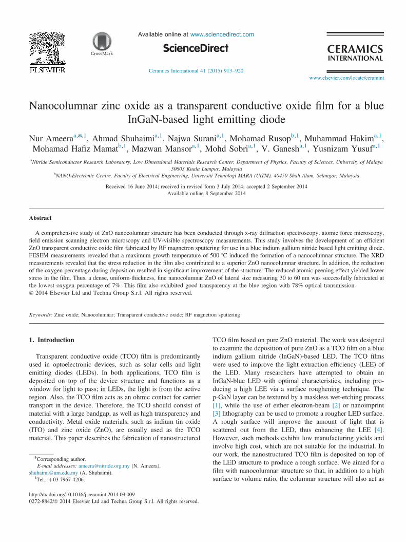
Fig. 1. (a). Phase analysis based on the XRD patterns of ZnO films depositedat 33% oxygen percentage and under various growth temperatures (RT to500 1C). Fig. 1(b). Phase analysis based on the XRD patterns of ZnO filmsdeposited at growth temperature of 500 1C and under varying oxygenpercentages (7–93%).
2. Experimental
The ZnO films were deposited onto Si(111) substrates usingradio-frequency (RF) magnetron sputtering. The substrateswere sequentially cleaned using acetone, propanol and deio-nized water and were blown dry with nitrogen gas. A ceramictarget of ZnO of 5 N purity was used for sputter deposition.Prior to each deposition, the target was pre-sputtered for 10minutes to remove the contaminants on the surface. The target-substrate distance was kept at 14 cm. The films were grown for1 hour using a fixed RF power of 200 W and a workingpressure of 5 mTorr. During deposition, the substrate holderwas rotated at 8 rpm to obtain a uniform ZnO layer. Argon andoxygen were used as discharge and reactive gases, respec-tively. Two conditions are considered for investigating thenanocolumnar structure of ZnO in this study: 1) maintainingthe oxygen at 33% from total percentage of argon and oxygenof 100% while varying the growth temperature from RT,100 1C, 200 1C, 300 1C, 400 1C and 500 1C, and 2) the growthtemperature was maintained at 500 1C while varying theoxygen percentage at 7%, 47%, 67% and 93%. The effectson the ZnO structural and morphological properties werecharacterized by x-ray diffraction (XRD) (Siemens D5000),atomic force microscopy (AFM) (Park System XE-100), fieldemission scanning electron microscopy (FESEM) (JOEL JSM-7600F), and UV-Visible spectroscopy (UV-Vis) (Perkin ElmerLambda 750 UV/Vis/NIR).
3. Results and discussion
Fig. 1(a) shows a phase analysis based on the XRD patternsof ZnO films deposited at 33% oxygen percentage and undervarying growth temperatures, TG (room temperature – 500 1C).All the deposited films exhibit a polycrystalline nature, withhigh and low intensity peaks at 341 and 651, respectively. Thepeaks at 341 and 651 were identified as (0 0 2) and (1 0 3)reflections of wurtzite structure, respectively, and are highlyc-axis oriented.By changing TG, a distinct (0 0 2) peak intensity variation
was observed, demonstrating the dependence of the ZnOstructural properties on the temperature during deposition[9]. However, the film orientation was not affected. Theintensity of the ZnO (0 0 2) peak became more intense andsharper with increasing TG up to 300 1C due to the improve-ment of the ZnO crystallinity. Meanwhile, when TG is greaterthan 300 1C, the intensity decreases gradually, which indicatesthat the degree of crystallinity of ZnO (0 0 2) is deteriorating.The observed trend is in agreement with most of the earlierstudies on ZnO deposited by RF sputtering [6,9,10]. The(0 0 2) peak intensity enhancement was observed at TG up to
N. Ameera et al. / Ceramics International 41 (2015) 913–920 915
300 1C due to the increase in the surface diffusion of theadsorbed atoms [6]. Furthermore, there a few reports indicatedan optimum (0 0 2) peak intensity occurring at 300 1C, whichis consistent with our data [10–12]. These results indicate thatmost ZnO film deposited at 300 1C is the highest quality interms of c-axis orientation for the ZnO crystallite.
Several possible reasons may be proposed for the corre-sponding peak variation in relation to TG. At TG below 300 1C,inadequate energy is provided to the atoms, thus reducing theirmobility [13]. There is a high possibility for the atoms to beincorporated at the incorrect lattice sites, thus preventingperfect crystallization in the ZnO films. High atom mobilityat high temperatures may allow the atoms to occupy moresuitable positions, thus enhancing crystallinity.
Re-evaporation of Zn and O atoms will be significant at TGgreater than 300 1C. In this case, higher energy is provided tothe atoms in the ZnO growth, causing the atoms to overcomethe binding energy and consequently leading to film re-evaporation. The higher TG also provides more energy to beheld by the sputtered atoms. These energetic atoms colliderapidly with the growing ZnO and the target. These collisionswith the atoms of the growing ZnO film lead to excessiveenergy being transferred to the collided atoms, leading to there-evaporation of ZnO [14]. Furthermore, the high energyincoming atoms may also embed into the growing ZnO film asimpurities [15]. It has also been reported that at highertemperatures, (0 0 2) peak degradation was attributed tomisorientation of the (0 0 2) planes with the substrate surface[12].
The average grain size, D; was calculated using the Scherrerformula:
D¼ Kλ
βcosθ
where K is a constant, set to 0.9; λ is the wavelength of theincident beam, 0.15406 nm; β is the full-width at half max-imum (FWHM) of the peak in radian; and θ is the Braggdiffraction angle [12].
The data in Table 1 indicates that the D value is in the rangeof 11–26 nm. This D value is much smaller than the real grainsize observed from the FESEM surface characterization, as
Table 1Grain size and interplanar spacing at different growth temperature and oxygenpercentage.
Growthtemperature (1C)
Oxygenpercentage (%)
Grain size,D (nm)
Planar spacing,d (Å)
RT 33% 20.8 2.656100 11.2 2.622200 15.6 2.649300 25.4 2.611400 14.8 2.626500 11.5 2.600500 7% 6.0 2.615
47% 10.0 2.62667% 10.6 2.61593% 14.6 2.634
shown in Fig. 2, which is in the range of 30–100 nm.However, the variation of the grain size increment anddecrement between the real and calculated D value is verysimilar. Per Table 1, a high D value is obtained at a TG of300 1C due to the smaller FWHM determined from thediffraction peak. The Bragg's angle, 2θϴ value for the(0 0 2) reflection is observed to be deviated from the reportedvalue for bulk ZnO (34.421); generally, this deviation isassociated with the presence of residual stress in the film.Thus, the interplanar spacing, d, of ZnO is associated withstress in the film.From Table 1, all the d values are observed to be larger than
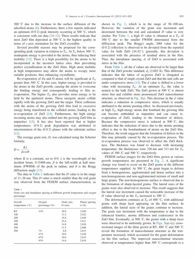
that of the ZnO powder standard, do (2.603 Å). This differenceindicates that the lattice of as-grown ZnO is elongated ascompared to that of single crystal ZnO and that the unit cells areunder compressive stress [13]. The d value is shifted to a lowervalue with increasing TG. At an optimum TG, the value isnearest to the bulk ZnO. The ZnO grown at 500 1C is almoststress free and exhibits more pronounced ZnO nanocolumnarstructure, as observed in Fig. 3(c). This decrease in the d valueindicates a reduction in compressive stress, which is usuallyattributed to the atomic peening effect. As discussed previously,at high TG, high-energy atoms that bombard the growing filmcan become embedded as impurities and can cause re-evaporation of ZnO, leading to the formation of defects.Because the compressive stress is reduced at 500 1C, thisindicates that the reduction of stress due to the atomic peeningeffect is due to the bombardment of atoms on the ZnO film.Therefore, the result suggests that the formation of defects in thefilm may primarily caused by the re-evaporation process. There-evaporation process was observed to affect the ZnO thick-ness. The thickness was found to decrease with increasingtemperature: the thicknesses were 326 nm and 311 nm for TGvalues of 300 1C and 500 1C, respectively.FESEM surface images for the ZnO films grown at various
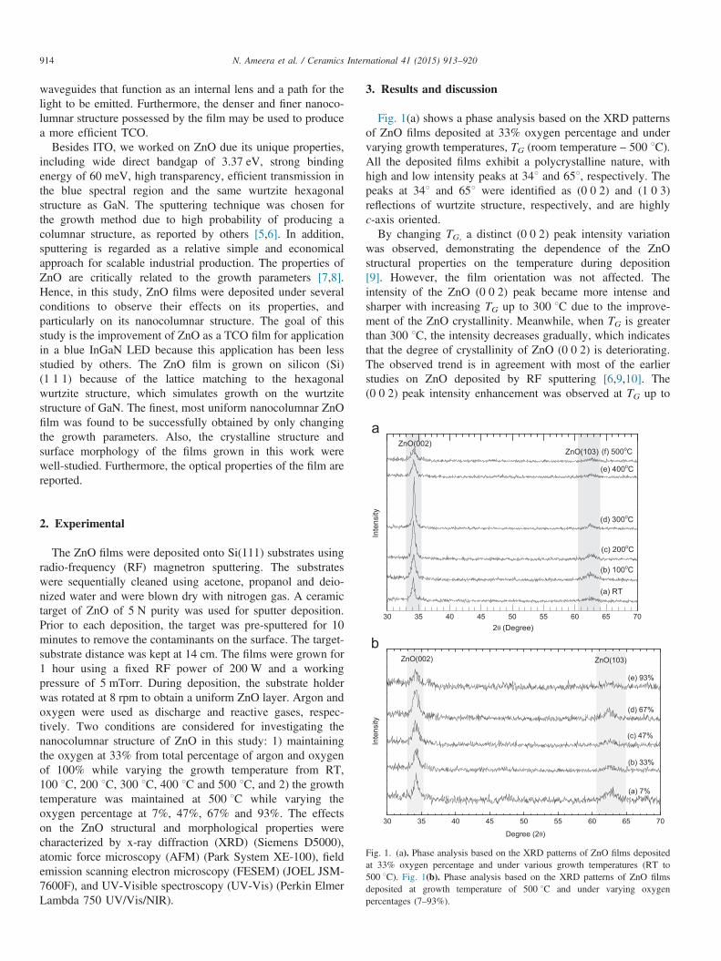
growth temperatures are presented in Fig. 2. A significantchange was found to occur on the ZnO grains at the differenttemperatures supplied. At 300 1C, the grain began to deformfrom a homogeneous, agglomerated and dense surface into anon-homogeneous and non-agglomerated mixture of small andlarge grains. The non-homogeneous surface is observed due tothe formation of sharp-faceted grains. The lateral sizes of thegrains were also observed to increase. This result suggests thatthe lateral size increment caused the noticeable increase of theD value observed as the TG increased to 300 1C.The deformation continues at TG of 400 1C, with additional
grains with sharp facet appearing on the film surface. Inaddition, the lateral sizes of the grains continue to increase.The grain size increment with the temperature is due to theenhanced kinetics, atomic diffusion and coalescence in theZnO film. Eventually, at 500 1C, the grains with a sharp facetwere observed to be uniformly grown. In Figs. 3(a)–(c), cross-sectional images of the films grown at RT, 400 1C and 500 1Creveal the formation of nanocolumnar structure as the tem-perature increased, which accounted for the grain deformationon the film surface. The improved nanocolumnar structureobserved at temperatures higher than 300 1C corresponds to a
Fig. 2. FESEM surface images for ZnO growth under varying growth temperatures at a fixed oxygen concentration of 33%. The image magnification is � 30,000.
Fig. 3. FESEM cross sectional images for ZnO growth under varying growth temperatures and oxygen percentages. The image magnification is � 100,000.
N. Ameera et al. / Ceramics International 41 (2015) 913–920916
higher grain boundary density. According to Hamad et al.,defects and adsorbed species are usually present at the grainboundaries [16]. Therefore, even though improved nanoco-lumnar structure is observed when ZnO is grown at hightemperature, defects dominated due to some factor thatdegrades the crystallinity. This degradation of crystallinitywas observed in our XRD results.
The AFM images in Fig. 4 are found to be in strongagreement with the surface FESEM images. During theformation of the nanocolumnar structure, the sharp facet grainsthat initially appeared at TG of 300 1C helped to increase thevertical size of the grains until 500 1C was reached. A larger
number of grains appeared at higher temperatures, resulting ina larger distribution of grains of high vertical size. Thus, thepeak to valley value increased accordingly, as presented inTable 2. The RMS roughness value also increased proportion-ally with TG due to the non-homogeneous ZnO surface.Next, the ZnO films were deposited at a fixed growth
temperature, TG of 500 1C, and under varying oxygen percen-tages (7–93%). Fig. 1(b) shows the phase analysis based on theXRD patterns of the deposited films. Similar to the ZnO filmsfor varying TG, the reflections of (0 0 2) and (1 0 3) appearedin the spectra. Changing the oxygen percentage was not foundto affect the ZnO crystal orientation. Furthermore, the (0 0 2)
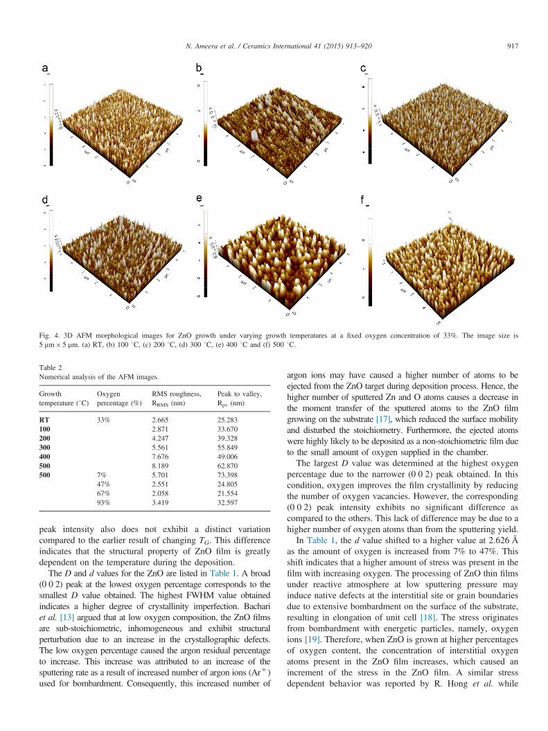
Fig. 4. 3D AFM morphological images for ZnO growth under varying growth temperatures at a fixed oxygen concentration of 33%. The image size is5 mm� 5 mm. (a) RT, (b) 100 1C, (c) 200 1C, (d) 300 1C, (e) 400 1C and (f) 500 1C.
Table 2Numerical analysis of the AFM images.
Growthtemperature (1C)
Oxygenpercentage (%)
RMS roughness,RRMS (nm)
Peak to valley,Rpv (nm)
RT 33% 2.665 25.283100 2.871 33.670200 4.247 39.328300 5.561 55.849400 7.676 49.006500 8.189 62.870500 7% 5.701 73.398
47% 2.551 24.80567% 2.058 21.55493% 3.419 32.597
N. Ameera et al. / Ceramics International 41 (2015) 913–920 917
peak intensity also does not exhibit a distinct variationcompared to the earlier result of changing TG. This differenceindicates that the structural property of ZnO film is greatlydependent on the temperature during the deposition.
The D and d values for the ZnO are listed in Table 1. A broad(0 0 2) peak at the lowest oxygen percentage corresponds to thesmallest D value obtained. The highest FWHM value obtainedindicates a higher degree of crystallinity imperfection. Bachariet al. [13] argued that at low oxygen composition, the ZnO filmsare sub-stoichiometric, inhomogeneous and exhibit structuralperturbation due to an increase in the crystallographic defects.The low oxygen percentage caused the argon residual percentageto increase. This increase was attributed to an increase of thesputtering rate as a result of increased number of argon ions (Arþ )used for bombardment. Consequently, this increased number of
argon ions may have caused a higher number of atoms to beejected from the ZnO target during deposition process. Hence, thehigher number of sputtered Zn and O atoms causes a decrease inthe moment transfer of the sputtered atoms to the ZnO filmgrowing on the substrate [17], which reduced the surface mobilityand disturbed the stoichiometry. Furthermore, the ejected atomswere highly likely to be deposited as a non-stoichiometric film dueto the small amount of oxygen supplied in the chamber.The largest D value was determined at the highest oxygen
percentage due to the narrower (0 0 2) peak obtained. In thiscondition, oxygen improves the film crystallinity by reducingthe number of oxygen vacancies. However, the corresponding(0 0 2) peak intensity exhibits no significant difference ascompared to the others. This lack of difference may be due to ahigher number of oxygen atoms than from the sputtering yield.In Table 1, the d value shifted to a higher value at 2.626 Å
as the amount of oxygen is increased from 7% to 47%. Thisshift indicates that a higher amount of stress was present in thefilm with increasing oxygen. The processing of ZnO thin filmsunder reactive atmosphere at low sputtering pressure mayinduce native defects at the interstitial site or grain boundariesdue to extensive bombardment on the surface of the substrate,resulting in elongation of unit cell [18]. The stress originatesfrom bombardment with energetic particles, namely, oxygenions [19]. Therefore, when ZnO is grown at higher percentagesof oxygen content, the concentration of interstitial oxygenatoms present in the ZnO film increases, which caused anincrement of the stress in the ZnO film. A similar stressdependent behavior was reported by R. Hong et al. while
N. Ameera et al. / Ceramics International 41 (2015) 913–920918
varying the oxygen composition during the sputtering process.When the oxygen partial pressure is low, the ZnO films exhibita significant decrease of the compressive stress, while the ZnOfilms exhibit a tensile stress when the argon partial pressure isabove 70% [12].
The d value shifted to 2.634 Å as the oxygen was increased to93%. Although the crystallinity is improved, a significant amountof stress is still present in the film. This stress is due to the excessoxygen introduced in the system that causes the atomic peeningeffects. C.W. Hsu et al. reported at high oxygen composition, ahigher number of neutral oxygen atoms are bombarding thegrowing films without low energy and causing implantation ordisplacement of the surface atoms deeper into the film [20]. Thisprocess caused the formation of intrinsic defects in the film.Therefore, the film crystallinity was ineffectively improved. Theenergetic particles bombardment onto the film caused the atomsto be tightly packed and may have caused a stress reversal fromtensile to compressive to occur.
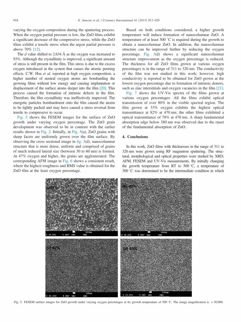
Fig. 5 shows the FESEM images for the surface of ZnOgrowth under varying oxygen percentage. The ZnO graindevelopment was observed to be in contrast with the earlierresults shown in Fig. 2. Initially, in Fig. 5(a), ZnO grains withsharp facets are uniformly grown over the film surface. Byobserving the cross sectional image in fig. 3(d), nanocolumnarstructure that is more dense, uniform and comprised of grainsof much reduced lateral size (between 30 to 60 nm) is formed.At 47% oxygen and higher, the grains are agglomerated. Thecorresponding AFM image in Fig. 6 shows a consistent result,where the highest roughness and RMS value is obtained for theZnO film at the least oxygen percentage.
Fig. 5. FESEM surface images for ZnO growth under varying oxygen percentage
Based on both conditions considered, a higher growthtemperature will induce formation of nanocolumnar ZnO. Atemperature of at least 500 1C is required during the growth toobtain a nanocolumnar ZnO. In addition, the nanocolumnarstructure can be improved further by reducing the oxygenpercentage. Fig. 3(d) shows a significant nanocolumnarstructure improvement as the oxygen percentage is reduced.The thickness for all ZnO films grown at various oxygenpercentages is in the range of 311 to 320 nm. The conductivityof the film was not studied in this work; however, highconductivity is reported to be obtained for ZnO grown at thelowest oxygen percentage due to formation of intrinsic donors,such as zinc interstitials and oxygen vacancies in the film [21].Fig. 7 shows the UV-Vis spectra of the films grown at
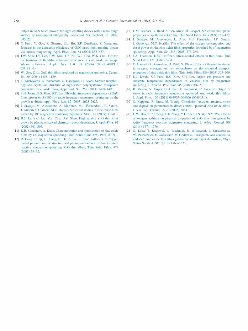
various oxygen percentages. All the films exhibit opticaltransmission of over 80% in the visible spectral region. Thefilm grown at 33% oxygen exhibits the highest opticaltransmittance at 82% at 470 nm; the other films exhibited aoptical transmittance of 78% at 470 nm. A sharp fundamentalabsorption edge below 380 nm was observed due to the onsetof the fundamental absorption of ZnO.
4. Conclusions
In this work, ZnO films with thicknesses in the range of 311 to326 nm were grown using RF magnetron sputtering. The struc-tural, morphological and optical properties were studied by XRD,AFM, FESEM and UV-Vis measurements. By initially changingthe growth temperature from RT to 500 1C, a temperature of300 1C was determined to be the intermediate condition in which
s at fix growth temperature of 500 1C. The image magnification is � 30,000.
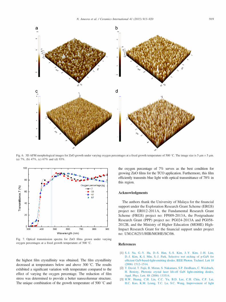
Fig. 6. 3D AFM morphological images for ZnO growth under varying oxygen percentages at a fixed growth temperature of 500 1C. The image size is 5 mm� 5 mm.(a) 7%, (b) 47%, (c) 67% and (d) 93%.
Fig. 7. Optical transmission spectra for ZnO films grown under varyingoxygen percentages at a fixed growth temperature of 500 1C.
N. Ameera et al. / Ceramics International 41 (2015) 913–920 919
the highest film crystallinity was obtained. The film crystallinitydecreased at temperatures below and above 300 1C. The resultsexhibited a significant variation with temperature compared to theeffect of varying the oxygen percentage. The reduction of filmstress was determined to provide a better nanocolumnar structure.The unique combination of the growth temperature of 500 1C and
the oxygen percentage of 7% serves as the best condition forgrowing ZnO films for the TCO application. Furthermore, this filmefficiently transmits blue light with optical transmittance of 78% inthis region.
Acknowledgments
The authors thank the University of Malaya for the financialsupport under the Exploration Research Grant Scheme (ERGS)project no: ER012-2011A, the Fundamental Research GrantScheme (FRGS) project no: FP009-2013A, the PostgraduateResearch Grant (PPP) project no: PG024-2013A and PG058-2012B, and the Ministry of Higher Education (MOHE) High-Impact Research Grant for the financial support under projectno: UM.C/625/1/HIR/MOHE/SC/06.
References
[1] S.-I. Na, G.-Y. Ha, D.-S. Han, S.-S. Kim, J.-Y. Kim, J.-H. Lim,D.-J. Kim, K.-I. Min, S.-J. Park, Selective wet etching of p-GaN forefficient GaN-based-light-emitting diodes, IEEE Photon. Technol. Lett 18(2006) 1512–1514.
[2] T. David, T. Fujii, B. Moran, S. Nakamura, S.P. DenBaars, C. Weisbuch,H. Benisty, Photonic crystal laser lift-off GaN light-emitting diodes,Appl. Phys. Lett. 88 (2006) 133514.
[3] H.W. Huang, C.H. Lin, C.C. Yu, B.D. Lee, C.H. Chiu, C.F. Lai,H.C. Kuo, K.M. Leung, T.C. Lu, S.C. Wang, Improvement of light
N. Ameera et al. / Ceramics International 41 (2015) 913–920920
output in GaN-based power chip light-emitting diodes with a nano-roughsurface by nanoimprint lithography, Semicond. Sci. Technol. 23 (2008)045022.
[4] T. Fujii, Y. Gao, R. Sharma, E.L. Hu, S.P. DenBaars, S. Nakamura,Increase in the extraction efficiency of GaN-based light-emitting diodesvia surface roughening, Appl. Phys. Lett. 84 (2004) 855–857.
[5] J.W. Shin, J.Y. Lee, T.W. Kim, Y.S. No, W.J. Cho, W.K. Choi, Growthmechanisms of thin-film columnar structures in zinc oxide on p-typesilicon substrates, Appl. Phys. Lett. 88 (2006) 091911–091913(091911-1).
[6] W. Gao, Z. Li, ZnO thin films produced by magnetron sputtering, Ceram.Int. 30 (2004) 1155–1159.
[7] T. Kuchiyama, K. Yamamoto, S. Hasegawa, H. Asahi, Surface morphol-ogy and crystalline structure of high-stable polycrystalline transparentconductive zinc oxide films, Appl. Surf. Sci. 258 (2011) 1488–1490.
[8] S.H. Jeong, B.S. Kim, B.T. Lee, Photoluminescence dependence of ZnOfilms grown on Si(100) by radio-frequency magnetron sputtering on thegrowth ambient, Appl. Phys. Lett. 82 (2003) 2625–2627.
[9] I. Sayago, M. Aleixandre, A. Martinez, M.J. Fernandez, J.P. Santos,J. Gutierrez, I. Gracia, M.C. Horillo, Structural studies of zinc oxide filmsgrown by RF magnetron sputtering, Synthetic Met. 148 (2005) 37–41.
[10] B.S. Li, Y.C. Liu, Z.S. Chu, D.Z. Shen, High quality ZnO thin filmsgrown by plasma enhanced chemical vapour deposition, J. Appl. Phys. 91(2002) 501–505.
[11] K.B. Sundaram, A. Khan, Characterization and optimization of zinc oxidefilms by r.f. magnetron sputtering, Thin Solid Films 295 (1997) 87–91.
[12] R. Hong, H. Qi, J. Huang, H. He, Z. Fan, J. Shao, Influence of oxygenpartial pressure on the structure and photoluminescence of direct currentreactive magnetron sputtering ZnO thin films, Thin Solid Films 473(2005) 58–62.
[13] E.M. Bachari, G. Baud, S. Ben Amor, M. Jacquet, Structural and opticalproperties of sputtered ZnO films, Thin Solid Films 348 (1999) 165–172.
[14] I. Sayago, M. Aleixandre, L. Ares, M.J. Fernandez, J.P. Santos,J. Gutierrez, M.C. Horillo, The effect of the oxygen concentration andthe rf power on the zinc oxide films properties deposited by rf magnetronsputtering, Appl. Surf. Sci. 245 (2005) 273–280.
[15] J.A. Thornton, D.W. Hoffman, Stress-related effects in thin films, ThinSolid Films 171 (1989) 5–31.
[16] O. Hamad, G. Braunstein, H. Patil, N. Dhere, Effect of thermal treatmentin oxygen, nitrogen, and air atmospheres on the electrical transportproperties of zinc oxide thin films, Thin Solid Films 489 (2005) 303–309.
[17] D.J. Kwak, K.I. Park, B.S. Kim, S.H. Lee, Argon gas pressure andsubstrate temperature dependences of ZnO:Al film by magnetronsputtering, J. Korean. Phys. Soc. 45 (2004) 206–210.
[18] R. Menon, V. Gupta, H.H. Tan, K. Sreenivas, C. Jagadish, Origin ofstress in radio frequency magnetron sputtered zinc oxide thin films,J. Appl. Phys. 109 (2011) 064905–064906 (064905-1).
[19] O. Kappertz, R. Drese, M. Wuttig, Correlation between structure, stressand deposition parameters in direct current sputtered zinc oxide films,J. Vac. Sci. Technol. A 20 (2002) 2084.
[20] C.W. Hsu, T.C. Cheng, C.H. Yang, Y.L. Shen, J.S. Wu, S.Y. Wu, Effectsof oxygen addition on physical properties of ZnO thin film grown byradio frequency reactive magnetron sputtering, J. Alloy. Compd 509(2011) 1774–1776.
[21] G. Luka, T. Krajewki, L. Wachniki, B. Witkowski, E. Lusakowska,W. Paszkowicz, E. Guziewicz, M. Godlewki, Transparent and conductiveundoped zinc oxide thin films grown by atomic layer deposition, Phys.Status Solidi A 207 (2010) 1568–1571.
Related Documents

![Enhancement of InGaN-Based Light Emitting Diodes ...InGaN-based light-emitting diodes (LEDs) are useful for a wide range of visible light applications [1]-[4]. They *Corresponding](https://static.cupdf.com/doc/110x72/60f8714d107e0617217e0a1d/enhancement-of-ingan-based-light-emitting-diodes-ingan-based-light-emitting.jpg)