Invited Presentations 13 Nanocarbon Field Emission Devices K. Subramanian, Y.M. Wong, W.P. Kang, J.L. Davidson , B.K. Choi, and M. Howell Department of Electrical Engineering & Computer Science, Vanderbilt University, USA We are fabricating and examining nanocarbon derived electron emission devices, specifically, nanodiamond lateral field emission diodes and gated carbon nanotube triodes. These novel microstructures provide interesting means of accomplishing electronics that are unaffected by temperature and radiation. Nanodiamond lateral field emitters have promise for high-speed and high-power applications with their small inter-electrode spacing and efficient emitter geometry [1] . The characteristic properties of nanocrystalline diamond including smaller grain size (5-10 nm), smoother surface morphology, increased sp 2 -carbon content and higher electrical conductivity are favourable for lateral field emitters. In this work, we report the fabrication process advancement and field emission behavior of the nanodiamond comb-shaped field emitter array in diode configuration. The nanodiamond lateral device was fabricated on a silicon-on-insulator (SOI) wafer. The lateral diode design includes arrays of high aspect-ratio nanodiamond emitter fingers arranged in a comb-like structure with spacing as small as 2 ?m from the nanodiamond anode (see Figure 1). The 9000-fingered lateral field emission diode (8 ?m anode-cathode spacing) exhibited a low turn-on voltage of 10 V (electric field: 1.25 V/?m) which is one of the lowest reported for lateral field emission devices, and a high emission current over 25 mA at an anode voltage of 260 V (field ~ 32 V/?m), Fig. 2. Also, we have recently demonstrated a FE triode amplifier, Figure 3, based on aligned carbon nanotubes (CNTs) synthesized by microwave plasma chemical vapor deposition method [2] . We have verified that the gated device with convex-shaped CNT emitters is a good triode amplifier with low gate leakage current, large dc gain of ~352, low gate turn-on voltage of ~25 V, and useful ac gain. Compared to other emitters, CNTs possess the advantages of very high aspect ratio, small radius of curvature, lack of vacuum-arcing, chemical inertness and thermal stability. Unlike TE-based triode, the high frequency operation of a FE triode is dictated by the cutoff frequency ( f T ) and not the electron transit time. Preliminary FE results, Figure 4, show that the improved triode amplifier array has a gate turn-on voltage of ~ 42 V and a very low gate leakage current of ~1% of the anode current. Fabrication and electrical performance of these configurations will be presented.

Welcome message from author
This document is posted to help you gain knowledge. Please leave a comment to let me know what you think about it! Share it to your friends and learn new things together.
Transcript

Invited Presentations
13
Nanocarbon Field Emission Devices K. Subramanian, Y.M. Wong, W.P. Kang, J.L. Davidson, B.K. Choi,
and M. Howell
Department of Electrical Engineering & Computer Science, Vanderbilt University, USA
We are fabricating and examining nanocarbon derived electron emission devices, specifically, nanodiamond lateral field emission diodes and gated carbon nanotube triodes. These novel microstructures provide interesting means of accomplishing electronics that are unaffected by temperature and radiation.
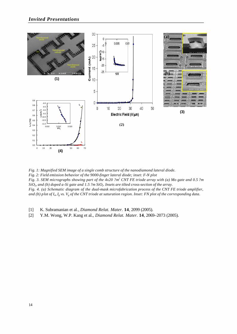
Nanodiamond lateral field emitters have promise for high-speed and high-power applications with their small inter-electrode spacing and efficient emitter geometry[1]. The characteristic properties of nanocrystalline diamond including smaller grain size (5-10 nm), smoother surface morphology, increased sp2-carbon content and higher electrical conductivity are favourable for lateral field emitters. In this work, we report the fabrication process advancement and field emission behavior of the nanodiamond comb-shaped field emitter array in diode configuration. The nanodiamond lateral device was fabricated on a silicon-on-insulator (SOI) wafer. The lateral diode design includes arrays of high aspect-ratio nanodiamond emitter fingers arranged in a comb-like structure with spacing as small as 2 ?m from the nanodiamond anode (see Figure 1). The 9000-fingered lateral field emission diode (8 ?m anode-cathode spacing) exhibited a low turn-on voltage of 10 V (electric field: 1.25 V/?m) which is one of the lowest reported for lateral field emission devices, and a high emission current over 25 mA at an anode voltage of 260 V (field ~ 32 V/?m), Fig. 2.
Also, we have recently demonstrated a FE triode amplifier, Figure 3, based on aligned carbon nanotubes (CNTs) synthesized by microwave plasma chemical vapor deposition method[2]. We have verified that the gated device with convex-shaped CNT emitters is a good triode amplifier with low gate leakage current, large dc gain of ~352, low gate turn-on voltage of ~25 V, and useful ac gain. Compared to other emitters, CNTs possess the advantages of very high aspect ratio, small radius of curvature, lack of vacuum-arcing, chemical inertness and thermal stability. Unlike TE-based triode, the high frequency operation of a FE triode is dictated by the cutoff frequency (fT) and not the electron transit time. Preliminary FE results, Figure 4, show that the improved triode amplifier array has a gate turn-on voltage of ~ 42 V and a very low gate leakage current of ~1% of the anode current.
Fabrication and electrical performance of these configurations will be presented.
Invited Presentations
14
Fig. 1: Magnified SEM image of a single comb structure of the nanodiamond lateral diode. Fig. 2: Field emission behavior of the 9000-finger lateral diode; inset: F-N plot Fig. 3. SEM micrographs showing part of the 4x20 ?m2 CNT FE triode array with (a) Mo gate and 0.5 ?m SiO2, and (b) doped a-Si gate and 1.5 ?m SiO2. Insets are tilted cross-section of the array. Fig. 4. (a) Schematic diagram of the dual-mask microfabrication process of the CNT FE triode amplifier, and (b) p lot of Ia, Ig vs. Vg of the CNT triode at saturation region. Inset: FN plot of the corresponding data. [1] K. Subramanian et al., Diamond Relat. Mater. 14, 2099 (2005). [2] Y.M. Wong, W.P. Kang et al., Diamond Relat. Mater. 14, 2069–2073 (2005).
(2)
(2)
0.0
0.1
0.2
0.3
0.4
0.5
0.6
0.7
0.8
0.9
0 10 20 30 40 50 60 70
Vg (V)
Ia, Ig
(?A
)
Ia
Ig
-11.0
-10.5
-10.0
-9.5
-9.0
-8.5
-8.0
0.010 0.015 0.0201/Vg
Ln
(Ia/V
g2 )
(1)
(3)
(4)
(b)
(a)
Related Documents