Glasgow Theses Service http://theses.gla.ac.uk/ [email protected] Nabi, Syed Waqar (2009) A coarse-grained dynamically reconfigurable MAC processor for power-sensitive multi-standard devices. EngD thesis. http://theses.gla.ac.uk/865/ Copyright and moral rights for this thesis are retained by the author A copy can be downloaded for personal non-commercial research or study, without prior permission or charge This thesis cannot be reproduced or quoted extensively from without first obtaining permission in writing from the Author The content must not be changed in any way or sold commercially in any format or medium without the formal permission of the Author When referring to this work, full bibliographic details including the author, title, awarding institution and date of the thesis must be given

Welcome message from author
This document is posted to help you gain knowledge. Please leave a comment to let me know what you think about it! Share it to your friends and learn new things together.
Transcript

Glasgow Theses Service http://theses.gla.ac.uk/
Nabi, Syed Waqar (2009) A coarse-grained dynamically reconfigurable MAC processor for power-sensitive multi-standard devices. EngD thesis. http://theses.gla.ac.uk/865/ Copyright and moral rights for this thesis are retained by the author A copy can be downloaded for personal non-commercial research or study, without prior permission or charge This thesis cannot be reproduced or quoted extensively from without first obtaining permission in writing from the Author The content must not be changed in any way or sold commercially in any format or medium without the formal permission of the Author When referring to this work, full bibliographic details including the author, title, awarding institution and date of the thesis must be given

A Coarse-Grained Dynamically
Reconfigurable MAC Processor for
Power-Sensitive Multi-Standard Devices
Syed Waqar Nabi B.S.Eng.
Institute for System Level Integration.
A thesis submitted to the Universities of Glasgow, Edinburgh,
Strathclyde, and Heriot-Watt
for the degree of
Doctor of Engineering in System Level Integration.
Copyright c© Syed Waqar Nabi
October 2008
In the name of Allah, the Beneficent, the Merciful.
Read: In the name of thy Lord Who createth, Createth man from
a clot. Read: And thy Lord is the Most Bounteous, Who teacheth
by the pen, Teacheth man that which he knew not. Nay, but verily
man is rebellious That he thinketh himself independent! Lo! unto
thy Lord is the return.
The Quran; Chapter 96, Verses 1–7
i
Abstract
DRMP, a Dynamically Reconfigurable MAC Processor, is an innovative, dy-
namically reconfigurable System-on-Chip architecture. The architecture ex-
ploits substantial overlaps in the functionality of different wireless MAC lay-
ers. Its flexibility is specialized for addressing the requirements of the MAC
layer of wireless standards. It is targeted at consumer, multi-standard, hand-
held devices, and its design is meant to address the balance of flexibility and
power-efficiency that this target market demands. The DRMP reconfigures
packet-by-packet on the fly, allowing execution of concurrent protocol modes
on a single hardware co-processor. An interrupt-driven programming model
has also been presented and shown to implement the protocol state-machine
of the three protocols on a CPU. These features will allow the DRMP to
replace three MAC processors in a hand-held device. The most innovative
component of the DRMP architecture is its Interface and Reconfiguration
Controller. It uses a combination of asynchronous controllers to dynamically
reconfigure the functional units in the architecture and delegate MAC tasks to
them. The architecture has been modeled in Simulink at cycle-approximate
abstraction. Results of simulations involving transmission and reception of
packets have been presented, showing that the platform concurrently han-
dles three protocol streams, reconfigures dynamically, yet meets and exceeds
the protocol timing constraints, all at a moderate frequency. Its heteroge-
neous and coarse-grained functional units, limited connectivity requirements
between these units, and proportionally large time that these resources are
idle, promise a very modest power-consumption, suitable for mobile devices,
while offering flexibility to implement different MAC protocols.
ii

Acknowledgments
I would like to first and foremost acknowledge the excellent support I received
from my academic supervisor, Dr. Wim Vanderbauwhede, and my industrial
supervisors, Dr. Cade Wells and Mr Bob Adamson. Their help and advice
was always sincere, helpful and practical. Their company was a pleasure,
and their persons, an example.
The Institute of System Level Integration in general, the EngD center and
Sian Williams in particular, deserve a special thanks. Also Alexandra (Sandy)
Buchanan who together with Sian Williams helped get things sorted out so
that I could join this course as an international student. Sandy had told me
then that at ISLI I will be well looked after, and indeed I was. I could not
have hoped for a better and more convenient place to do a doctorate than
ISLI.
To my wife Tahseen who joined me all the way from Bangladesh during my
EngD, and my daughter Sadiyah, who then came along and filled our lives
with diapers and happiness, thank you for your patience and support. It
could not have been the same without you.
To my all my family back home, for their support, and for their confidence
in me.
To Scotland, thank you! What a beautiful country you are, and what nice
people you have.
Last, I would like to acknowledge the Ministry of Science and Technology,
Government of Pakistan, and the people of Pakistan, who funded my studies.
iii

Publications during research
1. Nabi, S.W.; Wells, C.C.; Vanderbauwhede, W., “A dynamically recon-
figurable system-on-chip for implementing wireless MACs,” Research
in Microelectronics and Electronics Conference, 2007. PRIME 2007.
Ph.D. , vol., no., pp.37-40, 2-5 July 2007, Bordeaux, France.
2. Nabi, SW; Wells, CC; Vanderbauwhede, W, “Towards a Reconfigurable
SoC for Wireless MACs in Consumer Handheld Devices” First Inter-
national Conference on Computer, Control and Communication, pp.
182-191, 12-13 November 2007, Karachi, Pakistan.1
3. Nabi, Syed Waqar; Wells, Cade C.; Vanderbauwhede, Wim, “A Dy-
namically Reconfigurable Hardware Co-Processor for a Multi-Standard
Wireless MAC Processor,” Adaptive Hardware and Systems, 2008. AHS
’08. NASA/ESA Conference on , vol., no., pp.368-375, 22-25 June
2008, Noordwijk, The Netherlands.
4. Nabi, SW; Wells, C; Vanderbauwhede, W, “Interface and Reconfig-
uration Controller for a Wireless MAC oriented Dynamically Recon-
figurable Hardware Co-Processor” International Conference on Field
Programmable Logic and Applications, 2008 (FPL 2008), September
8-10 2008, Heidelberg, Germany.
5. Nabi, SW; Wells, C; Vanderbauwhede, W, “A Coarse-Grained Dy-
namically Reconfigurable MAC Processor for Power-Sensitive Multi-
Standard Devices” 21st International SOC Conference, September 17-
20 2008, Newport Beach, California, Unites States.
1This publication won an award for best paper in category.
iv

Dedication
Dedicated to my parents.
“Rabbirhamhuma Kama Rabba Yanee Saghira”
O Allah! Bestow on them your Mercy the way they had bestowed
mercy on me in childhood.
v

List of Abbreviations
2G . . . . . . . . . . . . . . . Second-generation wireless telephone technology
3G . . . . . . . . . . . . . . . Third-generation wireless telephone technology
ACK . . . . . . . . . . . . . Acknowledgment
AES . . . . . . . . . . . . . Advanced Encryption Standard
AMBA . . . . . . . . . . . Advanced Microcontroller Bus Architecture
API . . . . . . . . . . . . . . Application Programming Interface
ARQ . . . . . . . . . . . . . Automatic Repeat-reQuest
ASIC . . . . . . . . . . . . Application-Specific Integrated Circuit
ASIP . . . . . . . . . . . . Application Specific Instruction Processor
CID . . . . . . . . . . . . . Connection Identity
CLB . . . . . . . . . . . . . Configurable Logic Block
CPU . . . . . . . . . . . . . Central Processing Unit
CRC . . . . . . . . . . . . . Cyclic Redundancy Check
CS-RFU . . . . . . . . . Context-Switching RFU
CTS . . . . . . . . . . . . . Clear To Send
DES . . . . . . . . . . . . . Data Encryption Standard
DLL . . . . . . . . . . . . . Data Link Layer
DMA . . . . . . . . . . . . Direct Memory Access
DRMP . . . . . . . . . . . Dynamically Reconfigurable MAC Processor
DSP . . . . . . . . . . . . . Digital Signal Processor
DVFS . . . . . . . . . . . Dynamic Voltage and Frequency Scaling
EEPROM . . . . . . . . Electrically Erasable Programmable Read-Only Memory
FDD . . . . . . . . . . . . . Frequency-Division Duplex
FIFO . . . . . . . . . . . . First-In First-Out (Memory)
vi

FPGA . . . . . . . . . . . Field-Programmable Gate Array
Gbps . . . . . . . . . . . . Gigabit Per Second
HDL . . . . . . . . . . . . . Hardware Description Language
IC . . . . . . . . . . . . . . . Integrated Circuit
IC . . . . . . . . . . . . . . . Interface Controller
IEEE . . . . . . . . . . . . Institute of Electrical and Electronics Engineers
IP . . . . . . . . . . . . . . . Intellectual Property
IRC . . . . . . . . . . . . . . Interface and Reconfiguration Controller
ISA . . . . . . . . . . . . . . Instruction Set Architecture
LLC . . . . . . . . . . . . . Logical-Link Control
LUT . . . . . . . . . . . . . Lookup Table
MA-RFU . . . . . . . . Memory-Access RFU
MAC . . . . . . . . . . . . Media Access Layer
Mbps . . . . . . . . . . . . Megabit Per Second
MPDU . . . . . . . . . . . MAC Protocol Data Unit
MSDU . . . . . . . . . . . MAC Service Data Unit
OCT . . . . . . . . . . . . . Op-Code Table
OFDM . . . . . . . . . . . Orthogonal Frequency-Division Multiplexing
OSI . . . . . . . . . . . . . . Open Systems Interconnection
PAL . . . . . . . . . . . . . Programmable Array Logic
PCB . . . . . . . . . . . . . Printed Circuit Board
PCF . . . . . . . . . . . . . Point Coordinated Function
PHY . . . . . . . . . . . . . Physical Layer
PSO . . . . . . . . . . . . . Power Shut-off
QoS . . . . . . . . . . . . . Quality of Service
RC . . . . . . . . . . . . . . Reconfiguration Controller
RCA . . . . . . . . . . . . . Reconfigurable Communications Architecture (Intel)
RFU . . . . . . . . . . . . . Reconfigurable Functional Unit
RFUT . . . . . . . . . . . RFU Table
RHCP . . . . . . . . . . . Reconfigurable Hardware Co-Processor
RISC . . . . . . . . . . . . Reduced Instruction-Set Computer
RTL . . . . . . . . . . . . . Register Transfer Level/Language
RTS . . . . . . . . . . . . . Request To Send
vii

SDR . . . . . . . . . . . . . Software-Defined Radio
SiP . . . . . . . . . . . . . . System-in-Package
SoC . . . . . . . . . . . . . . System-on-Chip
SRAM . . . . . . . . . . . Static Random Access Memory
TDD . . . . . . . . . . . . Time-Division Duplex
TDM . . . . . . . . . . . . Time-Division Multiplexing
TH . . . . . . . . . . . . . . Task Handler
TH M . . . . . . . . . . . Task Handler for MAC Tasks
TH R . . . . . . . . . . . . Task Handler for Reconfiguration
UML . . . . . . . . . . . . Unified Modeling Language
UWB . . . . . . . . . . . . Ultra-Wideband
VC . . . . . . . . . . . . . . Virtual Component
WLAN . . . . . . . . . . Wireless Local Area Networks
WMAN . . . . . . . . . . Wireless Metropolitan Area Networks
WPAN . . . . . . . . . . . Wireless Personal Area Networks
viii

Contents
List of Figures xiii
List of Tables xvii
1 Introduction 1
1.1 Scope . . . . . . . . . . . . . . . . . . . . . . . . . . . . . . . 4
1.2 Target Markets . . . . . . . . . . . . . . . . . . . . . . . . . . 5
1.3 Innovation . . . . . . . . . . . . . . . . . . . . . . . . . . . . . 6
1.4 Thesis Outline . . . . . . . . . . . . . . . . . . . . . . . . . . . 7
2 Background 9
2.1 Feasibility . . . . . . . . . . . . . . . . . . . . . . . . . . . . . 10
2.2 An Overview of Reconfiguration Technologies . . . . . . . . . 17
2.2.1 Classification of Reconfigurable Architectures . . . . . 19
2.3 Wireless Standards . . . . . . . . . . . . . . . . . . . . . . . . 27
2.3.1 The MAC Sub-layer . . . . . . . . . . . . . . . . . . . 29
2.3.2 Analysis of Wireless Standards . . . . . . . . . . . . . 30
2.4 Related Work . . . . . . . . . . . . . . . . . . . . . . . . . . . 36
ix

3 System Architecture 44
3.1 Context . . . . . . . . . . . . . . . . . . . . . . . . . . . . . . 45
3.2 Design Considerations . . . . . . . . . . . . . . . . . . . . . . 46
3.2.1 Assumptions . . . . . . . . . . . . . . . . . . . . . . . . 46
3.2.2 Requirements and Constraints . . . . . . . . . . . . . . 47
3.3 Key Architectural Features . . . . . . . . . . . . . . . . . . . . 50
3.4 Classifying the DRMP Architecture . . . . . . . . . . . . . . . 51
3.5 System Partitioning . . . . . . . . . . . . . . . . . . . . . . . . 53
3.6 The Reconfigurable Hardware Co-processor . . . . . . . . . . . 58
3.6.1 The Interface and Reconfiguration Controller . . . . . . 60
3.6.2 The Reconfigurable Functional Units . . . . . . . . . . 68
3.6.3 Memories and Interconnect . . . . . . . . . . . . . . . . 74
3.6.4 Arbitration . . . . . . . . . . . . . . . . . . . . . . . . 80
3.6.5 RFU Trigger Logic and Master-Slave Mechanism . . . 82
3.6.6 Event Handler and Interface Buffers . . . . . . . . . . . 88
4 Using the DRMP Architecture 93
4.1 Programming Model . . . . . . . . . . . . . . . . . . . . . . . 93
4.1.1 The Interrupt-Driven Protocol Control . . . . . . . . . 95
4.1.2 API . . . . . . . . . . . . . . . . . . . . . . . . . . . . 96
4.2 Extended Instruction Set Architecture . . . . . . . . . . . . . 101
4.3 The DRMP as a Platform Architecture . . . . . . . . . . . . . 102
4.3.1 Platform-Based Design . . . . . . . . . . . . . . . . . . 102
4.3.2 Evolving DRMP into a Platform Architecture . . . . . 103
4.4 An Example of DRMP Application . . . . . . . . . . . . . . . 106
x
4.4.1 A Conventional Implementation . . . . . . . . . . . . . 107
4.4.2 Implementation on DRMP . . . . . . . . . . . . . . . . 107
5 Modeling and Simulation 117
5.1 Development Tools . . . . . . . . . . . . . . . . . . . . . . . . 117
5.2 Abstraction Level . . . . . . . . . . . . . . . . . . . . . . . . . 119
5.3 The Simulink Model . . . . . . . . . . . . . . . . . . . . . . . 120
5.4 Simulation Results . . . . . . . . . . . . . . . . . . . . . . . . 120
5.4.1 Simulation Run with One Protocol Mode . . . . . . . . 120
5.4.2 Simulation Run with Three Concurrent Protocol Modes 121
5.4.3 Results for the IRC . . . . . . . . . . . . . . . . . . . . 125
5.5 Discussion of Results . . . . . . . . . . . . . . . . . . . . . . . 128
5.5.1 Time Slack and Reducing Power Consumption . . . . . 129
5.5.2 Frequency of Operation . . . . . . . . . . . . . . . . . 130
5.5.3 Single Protocol vs. Three Concurrent Protocols’ Op-
eration . . . . . . . . . . . . . . . . . . . . . . . . . . . 131
5.5.4 The Interface and Reconfiguration Controller . . . . . . 133
5.5.5 Performance Assumptions (Software and Reconfigura-
tion) . . . . . . . . . . . . . . . . . . . . . . . . . . . . 136
6 Implementation Aspects 138
6.1 Area and Power Estimates . . . . . . . . . . . . . . . . . . . . 138
6.1.1 WiFi Estimates . . . . . . . . . . . . . . . . . . . . . . 139
6.1.2 UWB Estimates . . . . . . . . . . . . . . . . . . . . . . 140
6.1.3 WiMAX Estimates . . . . . . . . . . . . . . . . . . . . 141
6.1.4 DRMP Estimates . . . . . . . . . . . . . . . . . . . . . 142
xi

6.2 Power-Efficiency Improvements . . . . . . . . . . . . . . . . . 145
6.3 Utilization Potential and Limitations . . . . . . . . . . . . . . 149
6.3.1 Power-Efficiency . . . . . . . . . . . . . . . . . . . . . 150
6.3.2 Performance . . . . . . . . . . . . . . . . . . . . . . . . 151
6.3.3 Cost . . . . . . . . . . . . . . . . . . . . . . . . . . . . 152
6.3.4 Programmability and Extensibility . . . . . . . . . . . 152
6.4 Commercial Wireless MAC solutions . . . . . . . . . . . . . . 153
7 Conclusions 160
7.1 Future Architectural Exploration . . . . . . . . . . . . . . . . 163
7.1.1 System Design or Architectural Exploration . . . . . . 163
7.1.2 Synthesizing the Architecture to Lower Abstraction . . 165
A Snapshots of SIMULINK Model 166
B Detailed Comparison of Wifi, WiMAX and UWB 181
Bibliography 189
xii
List of Figures
1.1 Wireless Subscribers’ Growth . . . . . . . . . . . . . . . . . . 2
2.1 Abstract View of the RHCP . . . . . . . . . . . . . . . . . . . 11
2.2 The Binding Time vs Computation Space . . . . . . . . . . . 17
2.3 Static vs. Dynamic Reconfiguration . . . . . . . . . . . . . . . 20
2.4 Partial, Single and Multi-Context Reconfiguration . . . . . . . 21
2.5 The MAC Layer in Relation to Other OSI Layers . . . . . . . 30
2.6 Reconfigurable Packet Processing Wireless Nodes . . . . . . . 36
2.7 A Dynamically Reconfigurable Processor . . . . . . . . . . . . 38
2.8 General Network Architecture-Receiver . . . . . . . . . . . . . 39
2.9 Customized Network Arch. for IEEE 802.11 . . . . . . . . . . 40
2.10 Datapath Unit of the Chameleon Architecture . . . . . . . . . 41
2.11 QuickSilver’s Adaptive Computing Machine . . . . . . . . . . 42
3.1 The DRMP in a Multi-Standard Portable Device . . . . . . . 46
3.2 The DRMP SoC . . . . . . . . . . . . . . . . . . . . . . . . . 56
3.3 Abstract View of the RHCP . . . . . . . . . . . . . . . . . . . 59
3.4 The Interface and Reconfiguration Controller . . . . . . . . . . 61
3.5 Task-handler for Reconfiguration . . . . . . . . . . . . . . . . 64
xiii

3.6 Task-handler for MAC Operations . . . . . . . . . . . . . . . . 65
3.7 Reconf’n Controller . . . . . . . . . . . . . . . . . . . . . . . . 68
3.8 RFU Interface . . . . . . . . . . . . . . . . . . . . . . . . . . . 69
3.9 Packet Memory’s Map . . . . . . . . . . . . . . . . . . . . . . 76
3.10 Connection between the RFUs . . . . . . . . . . . . . . . . . . 79
3.11 Arbiter for the Packet Bus . . . . . . . . . . . . . . . . . . . . 81
3.12 Bus Grant Delay Logic . . . . . . . . . . . . . . . . . . . . . . 83
3.13 RFU Trigger Generation . . . . . . . . . . . . . . . . . . . . . 84
3.14 Slave RFU Trigger Options . . . . . . . . . . . . . . . . . . . 86
3.15 Transmission Buffer Control . . . . . . . . . . . . . . . . . . . 89
3.16 PHY Interface Wrapper . . . . . . . . . . . . . . . . . . . . . 90
4.1 Programming Model Alternatives . . . . . . . . . . . . . . . . 96
4.2 API for Programming the DRMP . . . . . . . . . . . . . . . . 98
4.3 API for Programming the DRMP (cont.) . . . . . . . . . . . . 99
4.4 Using the API . . . . . . . . . . . . . . . . . . . . . . . . . . . 100
4.5 Platform-Based Design Methodology . . . . . . . . . . . . . . 104
4.6 Conventional vs. DRMP Implementation . . . . . . . . . . . . 108
4.7 Transmission sequence diagram . . . . . . . . . . . . . . . . . 110
4.8 Wifi Interrupt Handler - 1 . . . . . . . . . . . . . . . . . . . . 115
4.9 Wifi Interrupt Handler - 2 . . . . . . . . . . . . . . . . . . . . 116
5.1 Packet Transmission - 1 Mode . . . . . . . . . . . . . . . . . . 122
5.2 Packet Reception - 1 Mode . . . . . . . . . . . . . . . . . . . . 123
5.3 Packet Transmission - 3 Modes . . . . . . . . . . . . . . . . . 124
5.4 Packet Reception - 3 Modes . . . . . . . . . . . . . . . . . . . 125
xiv

5.5 TH M Timing Diagram . . . . . . . . . . . . . . . . . . . . . . 127
5.6 TH R Timing Diagram . . . . . . . . . . . . . . . . . . . . . . 128
5.7 TH M Timing Diagram Magnified . . . . . . . . . . . . . . . . 129
5.8 Packet Transmission at 200 MHz . . . . . . . . . . . . . . . . 132
5.9 Packet Transmission at 50 MHz . . . . . . . . . . . . . . . . . 133
5.10 1 mode vs. 3 mode transmission . . . . . . . . . . . . . . . . . 134
5.11 Proportional time spent by a mode . . . . . . . . . . . . . . . 135
5.12 State occupation in the Task-handler . . . . . . . . . . . . . . 136
6.1 Time Slack in the RHCP . . . . . . . . . . . . . . . . . . . . . 146
6.2 Sequans SQN1010 WiMAX SoC . . . . . . . . . . . . . . . . . 155
6.3 Fujitsu MB87M3400 WiMAX SoC . . . . . . . . . . . . . . . . 156
6.4 Intel WiMAX Connection 2250 SoC . . . . . . . . . . . . . . . 157
6.5 Intel IXP 1200 Network Processor . . . . . . . . . . . . . . . . 157
A.1 Simulation Setup . . . . . . . . . . . . . . . . . . . . . . . . . 167
A.2 Model: DRMP top-level view . . . . . . . . . . . . . . . . . . 168
A.3 Model: Software statechart . . . . . . . . . . . . . . . . . . . . 169
A.4 Model: The Reconfigurable Hardware Co-Processor . . . . . . 170
A.5 Model: The Interface and Reconf’n Controller . . . . . . . . . 171
A.6 Model: The Task-handler for MAC . . . . . . . . . . . . . . . 172
A.7 Model: The Reconf’n Controller . . . . . . . . . . . . . . . . . 173
A.8 Model: The RFU Table . . . . . . . . . . . . . . . . . . . . . . 174
A.9 Model: The RFU Pool . . . . . . . . . . . . . . . . . . . . . . 175
A.10 Model: Inside the Crypto RFU . . . . . . . . . . . . . . . . . 176
A.11 Model: The stateflow chart of Crypto RFU . . . . . . . . . . . 177
xv

A.12 Model: The Packer bus arbiter . . . . . . . . . . . . . . . . . . 178
A.13 Model: The Tx-buffer statechart . . . . . . . . . . . . . . . . . 179
A.14 Model: The Debug subsystem . . . . . . . . . . . . . . . . . . 180
xvi

List of Tables
2.1 Comparison of Some Commercial Wireless Standards . . . . . 29
3.1 Classifying the DRMP Reconfigurable Architecture . . . . . . 52
3.2 Software / Hardware Interaction Mechanism . . . . . . . . . . 57
3.3 The op code table . . . . . . . . . . . . . . . . . . . . . . . . 62
3.4 The rfu table . . . . . . . . . . . . . . . . . . . . . . . . . . 63
3.5 Memory Architecture Options . . . . . . . . . . . . . . . . . . 92
4.1 RFUs expected to be used for WiFi, WiMAX and UWB . . . 111
5.1 Busy Time of Various Entities in DRMP During Transmission 126
5.2 Busy Time of Various Entities in DRMP During Reception . . 127
6.1 Synthesis Results - WiFi MAC . . . . . . . . . . . . . . . . . . 139
6.2 Gate Count for MAC Implementations . . . . . . . . . . . . . 142
6.3 Area of MAC Implementations . . . . . . . . . . . . . . . . . . 142
6.4 Power of MAC Implementations . . . . . . . . . . . . . . . . . 143
6.5 Estimates for the DRMP . . . . . . . . . . . . . . . . . . . . . 144
6.6 Commercial Solutions for Various Wireless Standards . . . . . 159
xvii

Chapter 1
Introduction
Recent years have seen a rapidly increasing demand in wireless-capable con-
sumer devices, as can be seen in the near exponential growth in wireless
subscribers in Fig. 1.1 [42]. This trend has been accompanied by an exten-
sive proliferation of multiple standards that are becoming increasingly faster
and more complex. Implementation of wireless capability for mobile devices
not only has to cope with multiple complex standards, it has to do so while
meeting the very strict requirements of the consumer hand-held device mar-
ket.
People expect to have wireless access to their devices and peripherals (Wire-
less Personal Area Network), wireless broadband internet access at home and
in the office (Wireless Local Area Network), and wireless broadband inter-
net throughout the city (Wireless Metropolitan Area Networks). This trend
towards ubiquitous communication requires the implementation of multiple
wireless standards in the same, small, battery-efficient device—hand-held or
laptop.
Wireless consumer devices hence place strict demands on implementation
platforms. The foremost demand, a result of the proliferation of wireless
standards, is to produce devices that can handle multiple wireless standards
(flexibility) and can seamlessly roam between them. They should also have
long battery lives (power efficiency), should provide high-speed data connec-
1

Chapter 1. Introduction
Worldwide Mobile Subscribers
0
500
1000
1500
2000
2500
3000
3500
2000 2001 2002 2003 2004 2005 2006 2007
Mill
ions
Figure 1.1: Growth of worldwide wireless subscriptions [42]
tivity (throughput/performance), and still be cost-effective. Moreover, with
wireless standards evolving so quickly, they also need to be able to bring
devices conforming to the new standards as quickly and as cost-effectively as
possible to remain competitive.
Such implementation platforms with flexibility to implement multiple stan-
dards with short time-to-market at a low price and low power consumption,
are required for both the Media Access (MAC) layer and the Physical (PHY)
layer of the wireless standards. It is now generally recognized that new circuit
design approaches are needed to deal with this required diversity of protocols
on a single hand-held device [52]. Domain-limited, heterogeneous reconfig-
urable architectures offer a solution that enable hitting the right balance of
power-efficiency and flexibility for mobile devices.
According to [3]
“Reconfigurable architectures that are just-flexible-enough to im-
plement all wireless modes offer a good compromise between low
cost, short time-to-market and low power consumption”
2

Chapter 1. Introduction
I have proposed such a reconfigurable hardware platform specialized for wire-
less standards: the Dynamically Reconfigurable MAC Processor (DRMP).
The aim is to develop a platform that can be reconfigured dynamically to
implement all MAC protocols of commonly used wireless standards. When
compared with a general purpose reconfigurable architecture like the Field-
Programmable Gate Array (FPGA), this domain-specific target allows im-
proved power-efficiency by trading off flexibility. In the current version of the
architecture, DRMP handles the packets of three protocols simultaneously
by allowing reconfiguration on a packet-by-packet basis. It was decided to
use Simulink by Mathworks as the development environment for quick archi-
tectural exploration and to co-simulate different parts of the architecture at
different abstraction levels.
The DRMP is a software / hardware partitioned platform in which the micro-
processor uses a Reconfigurable Hardware Co-processor (RHCP) to delegate
the data-flow and some critical control-flow to the hardware. The Central
Processing Unit (CPU) is left to deal primarily with the high-level control-
flow logic associated with running the protocol state-machine. This allows
the CPU to handle fast and complex MAC protocols while clocking at rela-
tively slow speeds, thus consuming less power than it would in a full software
implementation. The architecture on the whole is designed to be dynamically
reconfigurable. It will handle data streams of multiple (up to three) different
protocol standards, by reconfiguring itself on a packet-by-packet basis.
The architecture’s main innovation is in the design of the domain-limited Re-
configurable Hardware Co-Processor. Hardware co-processors are commonly
used to complement a microprocessing unit, but are generally either cus-
tomized, fixed logic, i.e. Application Specific Integrated Circuit (ASIC) , or
general-purpose reconfigurable logic (FPGA). While both improve through-
put, the former lacks flexibility while the latter is not power-efficient enough
for hand-helds.
The Hardware Co-Processor of the DRMP lies between these two extremes.
It targets a domain—the wireless Media-Access layers—and attempts to of-
fer the required flexibility of this domain at a power-efficiency better than
3
Chapter 1. Introduction
general-purpose reconfigurable logic like the FPGA or a full software imple-
mentation. Such a domain-specialized reconfigurable architecture is a feasi-
ble option for those domains that 1.) require power-efficient implementations
and 2.) can expect to have devices produced in larger numbers—thus allow-
ing economies of scale to ensure that a specialized architecture’s design and
fabrication is cost-effective. Solution for the MAC layer of wireless standards,
targeting consumer devices, is such a domain.
1.1 Scope
There are immense possibilities for research and innovation in the area of
reconfigurable platforms for wireless communications, and it was therefore
essential to find and define a scope that is both technically feasible and
commercially viable in the given time and resource constraints.
The project addresses the packet processing operations that are associated
the Media Access Control sub-layer of the Data Link Layer (DLL) of the
Open Systems Interconnection (OSI) seven-layer reference model [43]. The
operations carried out in this layer are distinctly different from those of the
PHY layer, and warrant investigation into an architecture that is optimized
for MAC operations.
The platform is dynamically reconfigurable amongst three wireless commu-
nication protocols. The multi-mode operation flexibility offsets the overhead
associated with programmability. Intel set its break-even target for reconfig-
urable architectures at three modes [71]. Choosing more than three proto-
cols was considered as introducing unnecessary complexity into the project.
There is however nothing in the architecture’s basic design that limits it to
three protocol modes.
The target is a reconfigurable platform for wireless consumer market, as op-
posed to the wireless infrastructure requirement. In many ways, the two
have very different characteristics and requirements. Consumer devices are
typically more power and cost sensitive, and have shorter life, than infras-
4

Chapter 1. Introduction
tructure devices. According to [67], the infrastructure market is better suited
for general-purpose reconfigurable hardware devices, while in the consumer
market more function-specific reconfigurable architectures may be employed
successfully.
The platform is also meant to be software programmable so that a different
set of three protocols can be implemented without any modifications to the
hardware. The project aims to make the platform as general as possible
so that the majority of prevalent wireless protocol MACs and their future
evolutions could be deployed. However, it was recognized that flexibility
is possible only to a certain limit beyond which the platform will cease to
be competitive by inefficient deployment of protocols. The more general-
purpose any reconfigurable platform is, the less efficient will be its resource
utilization for the deployment of a particular ‘mode’.
1.2 Target Markets
The platform is meant for hand-held / portable devices—devices where power
is an important consideration. For power-insensitive devices, the more at-
tractive option would be to implement the MAC entirely in software, which
offer a flexible and easy to program option.
It is meant to target multi-standard hand-held devices that need to ac-
cess multiple wireless standards at the same time. Such devices are al-
ready present in the market and the trend is towards greater integration
of standards in a single device. Eventually, this platform could be used for
Software-Defined Radios (SDRs); but that is not the main target and so the
considerations associated with SDRs will not be addressed in the project.
For example, an SDR by definition requires the complete protocol stack to
be software programmable. The DRMP, as will be discussed later, may not
necessarily be software programmable only. E.g. it may be that to implement
a certain MAC protocol on the DRMP platform, a derivative design of the
base platform may be needed, which will involve change in the actual silicon.
5

Chapter 1. Introduction
Also, the DRMP can contain FPGA logic, which requires development in a
Hardware-Design Language.
The DRMP is aimed at wireless protocols that can be typically expected in
consumer devices. So WiFi (IEEE Std. 802.11), Ultra-Wideband (UWB)
(IEEE Std. 802.15.3), WiMAX (IEEE Std. 802.16) are the protocols that
will be targeted. Protocols like Zigbee (IEEE Std. 802.15.4) which are not
designed for consumer devices are not considered.
The reason for aiming at consumer devices is that these devices tend to be
produced in very large numbers and in such scenarios the costs of fabri-
cating a new domain-targeted System-on-Chip (SoC) can be justified. The
economies of scale will ensure that the per-IC cost is feasible for cost-sensitive
consumer devices.
1.3 Innovation
The DRMP is designed based on well-established SoC design concepts. The
novelty in the DRMP lies at the system level; it is a completely unique archi-
tecture, designed from scratch, and aiming a particular domain. Following,
its key innovative aspects are highlighted:
• Aimed specifically at implementing the MAC layer of wireless stan-
dards, for consumer hand-held devices, and exploits the common func-
tionalities among different MAC layers is able to replace up to three
MAC processors on a device, by enabling dynamic, packet-by-packet
reconfiguration, and thus handling concurrent data streams of three
different protocols.
• Software controlled hardware co-processor, where the software runs the
protocol control only. The CPU never needs to directly access payload
data, which is handled entirely by the hardware. In a conventional
implementation where the hardware accelerator functions were slave
peripherals of the CPU, this would not be the case.
6

Chapter 1. Introduction
• A unique interrupt-driven software implementation of protocol control
of multiple standards concurrently on a single CPU.
• The hardware co-processor is dynamically reconfigurable on packet-
by-packet basis for 3 MAC protocols. Heterogeneous reconfiguration
mechanism for the RFUs.
• Clear partition of tasks between CPU and hardware, and coarse-grained
function-specific units result in a neat API allowing convenient software
programmability to implement different protocols.
These features will be discussed in detail later in the thesis. The Interface
and Reconfiguration Controller, in particular amongst them, is the most
innovative part of the architecture. This controller interfaces with the micro-
processor, accepting requests from three different protocol modes, and then
manages their execution on the available RFUs. The dynamic reconfigura-
tion of the RFUs is also controlled through a secondary controller inside this
main controller. In essence, it is the Interface and Reconfiguration Controller
that manages protocol modes executing concurrently on a single device with
shared resources, and the packet-by-packet reconfiguration. Its design is pre-
sented in section 3.6.1.
1.4 Thesis Outline
The thesis is organized in seven chapters, the first being the introduction to
the thesis. Chapter 2 starts with the project’s feasibility, and is followed by
background review of relevant subjects like reconfiguration technologies and
the MAC layer of wireless standards. Discussion of related work follows.
Chapter 3 presents the architectural details of the DRMP, after having first
discussed the requirements and constraints that guided the design. Chapter 4
discusses the use of DRMP architecture, explaining its programming model,
its extension as a platform architecture, and concluding with an example
7

Chapter 1. Introduction
of DRMP application. Next the modeling of the DRMP in Simulink and
simulation results are presented, and the results discussed, in chapter 5.
Chapter 6 discusses the implementation aspects of the DRMP architecture.
Area and power estimates for the DRMP are given, techniques for power-
efficiency improvements are discussed, DRMP’s utilization potential pre-
sented, and the chapter is concluded a presentation of and comparison with
some commercial wireless solutions. The last brief chapter presents the con-
clusions and future work. Appendices give snapshots of the Simulink model
and a tabulated and detailed comparison of the three MAC protocols con-
sidered for the prototype.
8

Chapter 2
Background
Multi-standard devices are a common consumer product today. Most third-
generation (3G) handsets support second-generation (2G) protocols for cov-
erage in areas that are not covered by 3G antennas. They typically also have
Bluetooth and infrared support. WiFi access is also becoming common.
Wireless technology typically addresses a particular usage scenario and there
are different protocol standards to address each scenario. But even within a
single usage model, one wireless protocol is not expected to dominate [94].
Solutions that can handle multiple protocols and switch between them have
become attractive.
In this context, reconfigurable hardware has been identified as suitable, but
the focus generally has been on the Physical layer of the protocol stack. How-
ever, if there is to be a reconfigurable platform for wireless communications,
the complete protocol stack has to be implemented on a flexible architecture.
The PHY and MAC layers are very different in the type of functions they
perform. The PHY layer is the more computationally intensive part of the
protocol stack. It concerns the device’s interaction with the network through
physical and electrical interfaces. It is a datapath-logic dominated layer
responsible for operations like modulation, filtering, error correction etc. The
MAC layer on the other hand is dominated by control operations. It is
therefore to be expected that the same architecture will not be suitable to
9

Chapter 2. Background
implement both the PHY and the MAC layer. For example, Tuan et al.
[89] have found lookup-table (LUT) structures typically found in FPGAs are
more suitable for the data-path dominated PHY layer while Programmable
Array Logic (PAL) architecture is more suitable for the control dominated
MAC layer, and proposes a hybrid structure for implementing the complete
protocol stack. Baschirotto et al. [4] note that the MAC-layer requires a
totally different architecture as compared to the digital baseband.
For the MAC layer, the flexibility requirement and its control-logic dominated
structure means that it generally is implemented by software. Intel’s Recon-
figurable Communications Architecture (RCA) is an example [14]. However a
software only implementation cannot offer both high performance and power-
efficiency. Panic et al. [65] estimate that a processor will need to run at 1
GHz to keep up with the real-time requirements of a WiFi MAC. This is a
drain on precious battery power. The situation will only get worse as higher
bandwidth protocols appear. The same job can be done on hardware or
hardware / software solution by clocking at much lower frequencies. FPGAs
are considered suitable for scenarios that require both flexibility and perfor-
mance, but they also incur a relatively heavy power and size penalty due to
the provision of high flexibility. Further, they take a long time to reconfig-
ure, typically in the order of milliseconds. An architecture with flexibility
limited to a particular domain offers a suitable trade-off between flexibility
and power-efficiency. Fig. 2.1 shows the trade-offs offered by various ar-
chitectures. A domain-limited reconfigurable architecture would lie on the
boundary between reconfigurable logic and dedicated hardware in this plane.
It is the kind of architecture increasingly being considered for devices which
need limited flexibility yet cannot afford the energy footprint of devices of-
fering general purpose flexibility like microprocessors or FPGAs.
2.1 Feasibility
This section briefly discusses the feasibility of designing a domain-specialized
reconfigurable architecture for the Wireless MAC layer. It is important to
10

Chapter 2. Background
Flexibility
Dedicated Hardware (ASIC)
Reconfigurable Logic
ASIPs, DSPs
Embedded Processors
Energy-effeciency MOPS/mW
0.1
1
10
100
1000
Figure 2.1: Energy efficiency versus flexibility trade off in various architec-tures [5]
establish both the technical and commercial feasibility of the project.
Wireless Technology is one of the most important technologies for now as
well as for the immediate future. Although wireless technology has been
used for a very long time, its only relatively recently that it has seen such
tremendous demand in the consumer world and correspondingly active and
rigorous research activity.
The demands on the industry have also increased with consumer expecta-
tions. Seamless roaming among different wireless standards is expected to
be the future of wireless technology for consumers. For example a typical
consumer hand-held wireless device will be able to switch from, say, WiFi
to WiMAX as the user moves from a WiFi hotspot to a WiMAX coverage
area. In the next to next generation wireless handsets, it is envisioned that
the user equipment and the wireless base station will dynamically switch the
wireless protocol they use (both the MAC and PHY) to make optimal use of
the volatile and unpredictable wireless environment - this will be the age of
Cognitive Radios [99]. In lieu of these trends, enabling technologies for the
following are of immense value to the consumer wireless electronics industry:
• Handling of multiple communication protocols.
11

Chapter 2. Background
• Switching amongst multiple protocols dynamically.
• Flexibility to implement new protocols or evolution of current proto-
cols.
• Making platforms energy, area and cost efficient.
• Enabling quick deployment by providing convenient high-level pro-
grammability and thus enabling companies to stay competitive with
short time-to-market.
The key enabling technology is the ability to make efficient multi-standard,
and future-proofed wireless hand-held devices based on software reconfig-
urable hardware platforms. This will not only allow seamless roaming, but
will also allow quick deployment of new protocols as they emerge. A platform
that can do this will be of immense value to the cut-throat wireless industry
where in order to remain competitive, it is essential to bring out products in
extremely short periods of time and still fulfill the consumers’ high expecta-
tions. Designing a platform that is efficient and flexible and can implement
the MAC operations of typical wireless protocols for consumer hand-held
devices thus has obvious commercial benefits, and can be designed using
reconfigurable hardware. As noted in [37]:
“As the time-to-market becomes shorter and various versions
of the same protocol are issued for covering new market needs
and trends, the MAC chips must be designed in order to be eas-
ily adapted to new protocol requirements. This desirable feature
of MAC processors increases the cost and power consumption of
the system, since the chip resources are not used efficiently, while
a static design could not always meet the new protocol require-
ments. Therefore the designer has to trade-off between efficiency
and flexibility for determining the final chip architecture.
A solution to this problem is to replace the dedicated hard-
ware by programmable logic that can be adapted to the protocol
12

Chapter 2. Background
requirements (and its newer versions) in a flexible and reliable
way. The reconfigurable hardware is easily adapted to new pro-
tocol requirements and may offer solutions optimized for speed,
area or power consumption according to system needs. The ma-
jor advantage of a reconfigurable solution is that the same logic
resources can be used for implementing different functions, de-
pending on the specific protocol functionality and this can be
done ‘on-the-fly’ by exploiting dynamic reconfiguration.”
Reduced time-to-market is also a very important goal achievable by using
reconfigurable hardware. According to [52], new designs have an yearly peak
sale cycle. If a vendor misses the window (out in August for peak sales in
November/December) then it will have to aim for next year by which time
the device may be obsolete. Vendors hence need to be able to bring out
complying devices very soon after a new protocol emerges.
Iliopoulos et al. [37] also mention two main disadvantages of using reconfig-
urable hardware: first, that it costs more than dedicated hardware for imple-
menting the same set of functions, and second, the long reconfiguration time.
The first problem can be solved by re-using the same reconfigurable hard-
ware resources for different protocols, thus increasing the functional density
of the device, as Iliopoulos et al. [37] also propose. DRMP solves the second
problem by using function-specific, coarse-grained reconfigurable functional
units that require very little configuration data to switch their state. These
aspects of the DRMP architecture will become clearer as the architecture
and a demonstrative simulation are discussed in later chapters.
It is interesting to note that most of the research on reconfigurable architec-
tures in the context of wireless communications has been carried out for the
computationally-intensive Physical layer. The MAC layer has generally been
implemented fully in software, and so programmability in the MAC layer
was generally a given. The PHY layer, because of its higher computational
requirements, needed platforms, programmable or otherwise, specialized for
the functionality of the PHY layer. So e.g. we have devices by picoChip,
13

Chapter 2. Background
like the PC102 [66], which is composed of an array of DSPs, and is opti-
mized for the Wireless PHY layer. Also, the Chameleon [76] architecture
and Quicksilver’s Adaptive Computing Machine [54] are examples of recon-
figurable architectures specialized for the functionality of the PHY layer.
Such specialized architectures for the MAC layer are not available. However,
in order to have dynamic switching between protocols, all of the protocol
stack has to be dynamically reconfigurable. Conventionally, the MAC has
been deputed completely to software. But the wireless MAC has very strict
real-time requirements and that means running the microprocessor at rel-
atively high frequencies with resulting large power consumption, rendering
them unsuitable for hand-held devices. Reconfigurable hardware has there-
fore potential application in the MAC layer as well. In fact Pionteck et al.
[67] consider the MAC layer the more suitable layer for using reconfigurable
logic.
FPGAs can be used for a flexible implementation of the MAC layer. They
are highly flexible, and they are also more energy-efficient than an equivalent
software implementation. However, for implementing MAC in wireless de-
vices, they do not make a feasible option. FPGAs tend to map inefficiently
to any problem with the typically less than 10% of chip area utilized for logic
[15], the remaining being devoted to routing resources. The interconnect re-
ources consume about 75-85% of the total power [13]. These overheads are
a result of FPGA’s provision of immense flexibility that requires full connec-
tivity between its configurable logic blocks. Such overheads are not feasible
in the context of power-sensitive hand-held devices. Also, only data-flow
dominated operations can be efficiently implemented on reconfigurable hard-
ware [67]. The MAC layer has considerable control logic, and it cannot fully
exploit the parallelism offered by FPGAs.
ASICs are not feasible in this scenario because they are by definition inflexible
and application-specific. Any upgrade to the protocol will require a new
ASIC with the associated development costs and risks. Structured-ASICs can
relieve the development costs, risks and time somewhat, but a new fabrication
process will nevertheless be needed whenever a new protocol comes along.
14
Chapter 2. Background
The problem with both software and FPGAs is that they are much more
flexible than would be required for a domain-limited reconfigurable MAC
platform and hence their associated overheads are not justifiable especially
in context of very power-conscious hand-held devices. Rabaey [74] notes
that, while sharing hardware between different protocol modes is essential
in a multi-standard device, general-purpose programmable components tend
to be three orders of magnitude less energy-efficient than custom implemen-
tation for the same function. A middle-path between general-purpose pro-
grammability and full-custom implementation clearly offers the best route.
It has been concluded therefore that a domain-specific reconfigurable archi-
tecture aimed specifically at the packet-processing operations of a wireless
MAC is a technically viable and as well as commercially attractive option.
Other researchers have supported this conclusion. Pionteck et al. [67] note
that changing specifications of the MAC layers results in that reconfiguration
is required for this layer, yet because power consumption and area overhead
are important, more function-specific reconfigurable architectures should be
used for the consumer market (as opposed to more general-purpose reconfig-
urable architectures for the infrastructure market).
Matching algorithms to architecture to achieve an optimum balance was pre-
dicted in [56]:
“ Advanced communication systems will be implemented as
reconfigurable, heterogeneous multiprocessor platforms. This hy-
pothesis is based on the fundamental trade-off between com-
putational efficiency (MOPS/mW)1 and flexibility. While pro-
grammable devices (.... -processors or DSPs) have the highest
degree of flexibility, they have at least a two to three orders of
magnitude smaller computationally efficiency than the intrinsic
computationally efficiency (ICE) of fixed architectures. Hence,
since power is the limiting factor, the SOCs of the future will
1Million operations per second per milliwatt.
15

Chapter 2. Background
carefully match algorithm with architecture to achieve an opti-
mum. (“Just as much flexibility as needed”). These SOCs will,
therefore, become application specific platforms. ”
16

Chapter 2. Background
2.2 An Overview of Reconfiguration Technolo-
gies
Digital electronics design engineers used to use either a microprocessor or
fixed logic for their embedded systems designs. With the prevalence of FP-
GAs, reconfigurable computing has emerged as another important design
paradigm (Fig 2.2) and an important building block for System-on-Chips.
As a concept, reconfigurable computing has been used for decades. For ex-
ample, even general purpose computers use a similar concept by reusing the
same functional blocks for different functions. But reconfigurable computing
that has been the intense focus of research in recent times has to do with the
actual hardware customization (rather than re-use of the same hardware) as
required by the application.
Binding Time?
Pre-Fabrication (Hardware)
Post-Fabrication (Software)
ASIC
Time
Computation in?
Reconfigurable
Processors
Space
Figure 2.2: ASICs, Microprocessors and Reconfigurable Hardware Relatedin the Binding Time vs. Computation Space [18]
ASICs allow a spatial distribution of tasks. On one hand, ASICs offer a low
power, area-efficient implementation of a task at (given enough items are
produced) a low cost. They also allow algorithms to execute very quickly
and are the natural choice for time-critical as well as power-conscious appli-
cations. The most obvious disadvantage of ASICs is that they are just that
- application specific. So the smallest change in the functional requirement
may require a new design with the huge associated costs and risks.
17

Chapter 2. Background
The prevalence of System-on-Chip design concepts has mitigated these costs
and risks to some extent by promoting extensive re-use. SoC technology
is the ability to place multiple functions or systems on a single chip. The
SoC design technology involves extensive re-use of pre-designed and verified
components, both hardware and software, which results in reduced develop-
ment time, costs and risks, when compared with conventional ASIC design
flow. However, unless reconfigurable fabric is included (which would make it
a System-On-a-Reconfigurable-Chip), an SoC is inflexible like an ASIC.
The inherent inflexibility combined with high development effort and costs
of ASICs and SoCs are rendering them unsuitable for many of today’s appli-
cations which require flexibility, cost-efficiency and a short time-to-market.
General-purpose processors on the other hand are entirely configurable and
hence flexible. But due to their sequential nature they are inherently less
efficient than ASICs. They also consume much more power and area than
ASICs for the same task since a huge amount of logic in a microprocessor is
‘support’ logic that is not performing the main task.
Reconfigurable computing provides the best of both worlds, so to speak.
It provides the performance benefits of hardware while still being flexible
like software by being reconfigurable post-fabrication. The synergy between
dynamic programmability and computational power makes reconfigurable
hardware a very attractive option to deploy computation-intensive tasks in
application fields that are constantly changing [10]. Fig 2.2 which has been
adapted from [18] compares these three different design paradigms.
It is important to make a distinction between configurable and reconfigurable
computing, which have been used by some authors interchangeably [8]. Re-
configurable systems imply a system that is configurable repeatedly while its
running, or while its stopped for a short while. It is possible that a system is
configurable because the hardware can be configured at compile-time or once
after manufacturing, but it will not be reconfigurable.
18

Chapter 2. Background
2.2.1 Classification of Reconfigurable Architectures
Although FPGAs are the commercially dominant reconfigurable platform,
it would be a mistake to restrict the study of reconfiguration to FPGAs.
Numerous architectures have been proposed and developed over the years.
This field is vast in its scope with many degrees of freedom. It was therefore
important to fully understand and appreciate the various types of dynami-
cally reconfigurable architectures. Appreciation of these lines of classification
and the respective pros and cons helped in making the correct architectural
choices. Different authors have classified reconfigurable architectures in dif-
ferent ways. See [8], [12], [30], [80] and [75]. I have made use of these
classifications to come up with a list of ‘classifiers’ that are considered as
important in making design decisions for the platform that is being devel-
oped. They are discussed here briefly and interested readers can look up
these references for more detailed information of this exciting subject.
2.2.1.1 Binding Time—Static vs. Dynamic Reconfigurability
Binding time specifies the point at which an architecture becomes ‘bound’ to
a specific implementation. It is a useful yardstick along which the complete
family of digital hardware from ASICs to microprocessors [18] can be classi-
fied. In case of a microprocessor, the binding time is just before execution
of an instruction. The architecture (i.e. the microprocessor) is not bound
to a particular implementation until an instruction is fetched and decoded.
ASICs are bound to an implementation when its masks have been fabricated.
For reconfigurable computing, the binding time can be at various stages
between these two extremes. For an FPGA for e.g., the binding time is
typically when the device is started up, although effectively—unless it is
multi-context—it is bound to a certain configuration at compile-time. This
is also called static reconfiguration and is typically associated with traditional
FPGAs. It is also possible to halt the functionality of an FPGA-type device
and then reconfigure it dynamically for a new task (without re-compilation
i.e.), and in this case it can be said that the binding time is dynamic on
19

Chapter 2. Background
a per-task basis. It is also possible to bind the reconfigurable architecture
run-time on a cycle-by-cycle basis which is a more extreme case of dynamic
reconfiguration, e.g. Quicksilver’s Adaptive Computing Machine (ACM) [71,
53]. Fig 2.3 (adapted from [8]) illustrates the distinction between static and
dynamic reconfiguration.
Design Configurations
Configure Logic
Execute
Design Configurations
Configure Logic
Execute
Design Configurations
Configure Logic
Execute
Design Configurations
Configure Logic
Execute
Figure 2.3: The Distinction between Static (top) and Dynamic Reconfigura-tion [8]
2.2.1.2 Configuration Arrangement
Reconfiguration can be achieved by different mechanisms. The following
classification has been derived from [12].
• Simple choice: Selection between one of several blocks. (See sec-
tion 2.2.1.4)
• Definition Through Arrangement: The functionality of the system is
defined by the interconnection of blocks. (E.g. [91])
• Definition through Alteration: In this case the blocks are themselves
programmable or paremetrizable in addition to the flexible intercon-
nect.
20
Chapter 2. Background
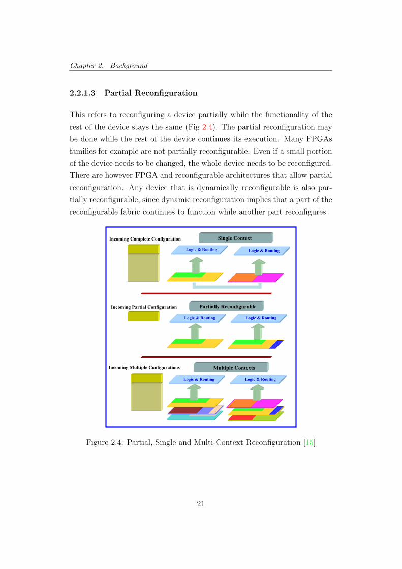
2.2.1.3 Partial Reconfiguration
This refers to reconfiguring a device partially while the functionality of the
rest of the device stays the same (Fig 2.4). The partial reconfiguration may
be done while the rest of the device continues its execution. Many FPGAs
families for example are not partially reconfigurable. Even if a small portion
of the device needs to be changed, the whole device needs to be reconfigured.
There are however FPGA and reconfigurable architectures that allow partial
reconfiguration. Any device that is dynamically reconfigurable is also par-
tially reconfigurable, since dynamic reconfiguration implies that a part of the
reconfigurable fabric continues to function while another part reconfigures.
Logic & Routing
Incoming Complete Configuration
Incoming Partial Configuration
Incoming Multiple Configurations
Logic & Routing
Logic & Routing Logic & Routing
Logic & RoutingLogic & Routing
Single Context
Partially Reconfigurable
Multiple Contexts
Figure 2.4: Partial, Single and Multi-Context Reconfiguration [15]
21
Chapter 2. Background
2.2.1.4 Single-Context vs. Multi-Context Reconfigurable Archi-
tectures
This is a very important differentiating factor for reconfigurable architec-
tures. A single-context reconfigurable architecture will have, at any time,
only one context ‘loaded’ onto the architecture. If some different function-
ality is required of the architecture, the architecture has to be reconfigured
which typically means loading a new bit-stream into the platform’s switch-
ing Static Random Access Memories (SRAMs) and LUTs. Most commercial
FPGAs fall into this category.
A multi-context platform on the other hand has multiple contexts ‘loaded’
onto the platform at configuration time (Fig 2.4). It can also be considered
as “loading multiple memory bits for each programming bit location” [15].
One of the contexts is active while the others are dormant although still re-
siding on the platform. A dormant context can become active by a simple
switching event, and the device is reconfigured. There is no need to load a
new bit-stream and this means extremely fast-switching is possible - on cycle-
by-cycle basis if required - reducing the reconfiguration time to the order of
nanoseconds from the milliseconds typically associated with single-context
reconfiguration. There is however the overhead of storing the multiple con-
texts on the platform. It is possible to do “background loading” [15] where
one context is active while another is in the process of being programmed for
later activation. A commercial product that uses this technique is CS2000
RCP series from Chameleon Inc. Other examples are in [79]. A concept
similar to having multiple contexts is to have a reconfiguration cache on the
chip [79].
2.2.1.5 Global vs. Local Run-Time Reconfigurability
Another differentiating aspect of reconfigurable devices is whether they are
reconfigured locally or globally. Locally here means that a sub-set of the re-
configurable fabric is assigned to a particular application and another subset
is assigned to another application - several configurations can exist simulta-
22

Chapter 2. Background
neously. Global reconfiguration implies that the whole architecture is con-
figured towards the accomplishment of the same task or application. This
‘one configuration at a time’ is suitable for applications that have several
operational modes or that are naturally divisible into sequential phases [75].
2.2.1.6 Homogeneous vs. Heterogeneous Architectures
Most commercial reconfigurable platforms like FPGAs are homogeneous.
That is, a reconfigurable element is identically reproduced throughout the
architecture, making it homogeneous. A homogeneous architecture in terms
of the functional elements also implies a homogeneous interconnect archi-
tecture. FPGAs are typically homogeneous architectures. Heterogeneous
architectures on the other hand contain reconfigurable elements that may
or may not be reproduced identically throughout the platform. They may
be of different sizes and that implies an irregular interconnect structure.
The concept of homogeneous and heterogeneous architectures is quite closely
linked with the categorization of architectures as general-purpose or domain-
specific. Domain-specific platform generally have heterogeneous blocks.
2.2.1.7 Granularity of Architectures
Granularity is described as the smallest functional unit that is reconfigurable
by the mapping tools. Fine-grained architectures are more flexible but will
have area overheads for interconnect (i.e. will have low functional density)
and larger delays. Coarse-grained architectures can lead to relatively effi-
cient implementations if the intended functionality matches well with the
architecture of the functional units. They minimize the overheads that are
caused by routing and configuration channels that affect more fine-grained
architectures like FPGAs [10].
However, they are less adaptable than finer-grained architectures. The gran-
ularity is also linked with how general-propose or domain-specific an architec-
ture is. In general it can be said that the more general-purpose and flexible
23
Chapter 2. Background
we want an architecture to be, the more fine-grained we will have to make
it. FPGAs are an example of fine-grained architectures, programmable at
bit-level, and highly flexible.
On the other hand, we have architectures like picoChip’s PC102 [66]. It is a
programmable processor optimized for the high capacity wireless digital sig-
nal processing applications. It consists of an array of RISC processors, which
makes it a very coarse-grained processor, but also makes it optimized for a
specific kind of application. Same goes for architectures like the Chameleon
[76] and Quicksilver’s Adaptive Computing Machine [54], which are coarse-
grained architectures specialized for particular application domains. Stretch
offer their S6000 family of software configurable processors [84]. They con-
tain a VLIW processor core and a configurable Instruction Set Extension
Fabric that is very coarse-grained, performing thousands of operations as a
single instruction.
2.2.1.8 Coupling with Host Architecture
A reconfigurable platform’s coupling to a host controlling processor can vary
from very tightly coupled to loosely coupled. On one end of the extreme is
reconfigurable functional elements in a processor that form a part of the pro-
cessor’s execution pipeline, i.e. tight on-chip coupling [31]. On the other end
is a stand-alone platform that is remotely controlled by a processor over a net-
work. Between these two extremes lies the case of a reconfigurable platform
acting as a co-processor or a hardware accelerator to the main processor.
2.2.1.9 Control
This refers to the control of reconfiguration on the platform. Carter [12] has
discussed the various possibilities:
• Central, external and intelligent: New configurations are deployed by
an external controller, e.g. the host processor in an SoC.
24

Chapter 2. Background
• Central, internal and intelligent: The reconfigurable architecture re-
configures itself through its own controller that responds to external
stimuli.
• Distributed and intelligent: Each part can decide its own rearrange-
ment, and that of others as well.
• Distributed and unintelligent: The part are modified in response to
external stimuli according to some predefined rules.
2.2.1.10 General-Purpose vs. Domain-Specific
This is a pretty much self-explanatory classification. A general-purpose plat-
form will not be optimized for a particular domain and hence will map ineffi-
ciently to the application deployed on it. It has the advantage of being very
flexible at the cost of this inefficiency. A domain-specific platform makes the
inverse trade-off. It improves its efficiency at the cost of flexibility (Fig. 2.1).
This is an important trade-off and is a critical design consideration for a
platform. It also effects other design consideration that have been discussed
in this section e.g. granularity and homogeneity.
2.2.1.11 Interconnect
With the continued reduction in gate area and energy-consumption, the in-
terconnect has begun to play a proportionally dominant role in the energy
requirements of an SoC. The reason is that the energy for on-chip communi-
cation does not scale down with device scaling [6]. The same effect is even
more pronounced in reconfigurable architectures which tend to have complex
and area-consuming interconnects because of the need to accommodate flex-
ible routing maps. In FPGAs for example, the interconnect typically takes
more than 60% of the silicon. It is therefore a critical design issue for reconfig-
urable architectures and an active area of research. The main consideration
for reconfigurable platforms’ interconnects is that they should be flexible and
hence able to handle different patterns of interconnects at compile-time or
25

Chapter 2. Background
run-time depending on which kind of reconfiguration they are aiming for.
FPGAs typically employ an island structure with connect-boxes and switch-
boxes. This allows any element to connect to any other and allows relatively
straightforward delay estimates.
An alternative interconnect architecture is a reconfigurable mesh model [7].
In a 4x4 mesh, the reconfigurable elements are connected to their four neigh-
bors (North, South, East and West). The functional elements can process
data coming in at one end and pass it out another, but they can also choose
to simply pass it on without any processing and thus act like a router. The
connectivity is limited as compared to FPGAs but results in huge reductions
in interconnect overheads. An all-together different paradigm has been sug-
gested for the use in SoCs and also in reconfigurable architectures. That is of
using a ‘connection-less’ packet-based network on the chip for communication
between entities, i.e., a Network-on-Chip (NoC). An example is the Gannet
architecture [91] which views the reconfigurable architecture as a Data-flow
architecture with ‘services’ connected by an NoC working together to provide
a specific functionality.
26

Chapter 2. Background
2.3 Wireless Standards
The technology for wireless data communications has been progressing con-
stantly from research to standardization and implementation, guided by
Shannon’s law and Moore’s Law. Wireless standards have evolved very
swiftly over the past years. The consumer expectations is driving the need
for efficient protocols capable of handling broadband speeds for multi-media
streaming and other demanding applications. All domains of wireless com-
munications - i.e. Personal Area Networks (WPANs), Local Area Networks
(WLANs) as well as Metropolitan and Wide Area Networks (WANs) have
seen tremendous activity and advancements. Standardization has led to mass
production of wireless consumer devices at affordable prices so much so that
they are now an integral part of life in the developed countries.
In the domain of Personal Area Networks, the dominant standard is Blue-
tooth which has been standardized by IEEE as 802.15.1. The current stan-
dard has speeds of up to 2 Mbps. However, IEEE developed a new standard,
the IEEE Std 802.15.3 [32], which was called ‘High Rate WPAN’ and was
meant to provide speeds of up to 20 Mbps using Ultra-Wideband technology
(UWB). It was meant to support real-time multimedia streaming thus open-
ing new demanding markets to Bluetooth which has typically been associated
with low bandwidth services like voice, control, and low-speed data. However,
as a result of failure to reach an agreement on the standardization of this pro-
tocol amongst the stake holders, the IEEE Std. 802.15.3 task group was shut
down without conclusion. For the purpose of this research, i.e. looking at a
representative set of MAC protocols typically used in consumer devices, and
investigating functional similarities and differences, continued investigation
of the MAC protocol of IEEE Std. 802.15.3 was deemed appropriate.
Wireless Local Area Networks is prevailed by the IEEE Std 802.11 [33],
branded as Wireless Fidelity or WiFi. Work on the first standard started
in 1990 and since then a number of PHY layers have been standardized to
meet the increasing bandwidth demands of the consumer electronics industry.
Six physical layers are currently defined. WiFi was widely criticized for its
27

Chapter 2. Background
security loopholes and later amendments have tried to address this issue. A
very recent development is the introduction of a new MAC layer (earlier, all
PHY layers used the same MAC layer) that provides Quality of Service (QoS)
support for multimedia applications. The corresponding standard 802.11e
was approved in 2005. Another task group (N) is working on a high-speed
physical layer based in Orthogonal Frequency-Division Multiplexing (OFDM)
technology. It is expected to provide speeds of up to 100 Mbps [35].
A protocol that is expected to become as pervasive is WiFi, and directly
compete with 3G standards, is the WiMAX, standardized as IEEE Std
802.16 [34] . It is a standard for broadband wireless access in Metropolitan
Area Networks. The first standard was approved in 2001 and since then
has been followed by many amendments. The latest standard is IEEE Std
802.16e-2005 which follows on from the IEEE Std 802.16-2004. This latest
standard is a big leap from previous ones in that it allows mobile broadband
wireless access - it is the Mobile WiMAX. This brings it in direct competition
with 3G and High-Speed Downlink Packet Access (HSDPA), and it is said
this will unleash the true potential of WiMAX. A protocol very similar to the
Mobile WiMAX, WiBro is already up and running in South Korea since June
2006 [64]. Mobile WiMAX has been deployed for the first time in Pakistan
by Motorola [96]. Intel has put its weight behind WiMAX and is embedding
WiMAX into its laptops like it does for WiFi. WiMAX is undoubtedly a
protocol that is going to become widespread but exactly to what extent is a
matter of debate.
Although there are numerous other protocols, these three protocols, WiFi,
WiMAX and UWB, have been discussed since they are or promise to become
pervasive and after considerable survey they have been chosen to be used to
design the 3-mode reconfigurable MAC processor. Table 2.1 [24] gives a
comparative analysis of available wireless standards.
Fourty et al. [24] discuss these wireless standards with special emphasis on
comparison between WiFi and WiMAX.
28

Chapter 2. Background
CommercialName
Standard TheoreticalData Rates
Max Range Frequency(GHz)
RFID ISO14443
106 Kbps 3 m Several
Bluetooth IEEE802.15.1
Mbps 100 m 2.4
UWB IEEE802.15.3
Up to 50 Mbps 10 m 2.4
Zigbee IEEE802.15.4
20 and 250Kbps
10 and 75 m 2.4 and 0.9
WiFi IEEE802.11
Various, from11 to 320 Mbps
From 30 to100 m
0.9, 2.4 and5.5
WiMAX IEEE802.16
70 Mbps 50 km 2.5 3.5 5.8
3GSM UMTS 21 Mbsp (withHSDPA)
Varied tosuit. Upto200 km
Variousbands be-tween 1.7 and2.2
Table 2.1: Comparison of Some Commercial Wireless Standards
2.3.1 The MAC Sub-layer
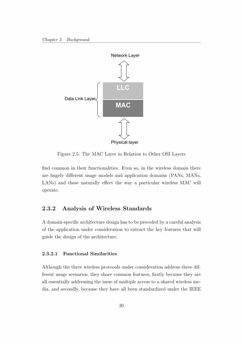
Wireless communication protocols are mostly defined for the lower two layers
of the 7 layer OSI reference model for communication protocols (Figure 2.5);
that is, the Data Link Layer and the Physical Layer. A sub-set of the Data-
Link layer is the MAC layer, i.e. the Media Access Layer.
The prime purpose of this layer is to ensure fair access to a shared medium.
It also takes on some other roles like handling redundancy and encryption. In
the context of wireless protocols, the MAC layer has yet additional responsi-
bilities. There is an extra requirement for providing security from eavesdrop-
pers (privacy) and illegal access to resources (authentication). Also, due to
higher chances of data corruption/distortion during transmission, and also
the unpredictability of wireless environment, flexible methods for handling
errors (e.g. fragmentation) are needed. All these requirements make the
typical Wireless MAC a fairly complex entity.
All wireless MAC protocol address similar issues, hence there is a lot one can
29
Chapter 2. Background
MAC
LLC
Physical layer
Network Layer
Data Link Layer
Figure 2.5: The MAC Layer in Relation to Other OSI Layers
find common in their functionalities. Even so, in the wireless domain there
are hugely different usage models and application domains (PANs, MANs,
LANs) and these naturally effect the way a particular wireless MAC will
operate.
2.3.2 Analysis of Wireless Standards
A domain-specific architecture design has to be preceded by a careful analysis
of the application under consideration to extract the key features that will
guide the design of the architecture.
2.3.2.1 Functional Similarities
Although the three wireless protocols under consideration address three dif-
ferent usage scenarios, they share common features, firstly because they are
all essentially addressing the issue of multiple access to a shared wireless me-
dia, and secondly, because they have all been standardized under the IEEE
30

Chapter 2. Background
802 family.
In some cases, the overlap is exact, such that a functional unit for one pro-
tocol MAC can be used as-is for another. An example would be the Header
Integrity Check for WiFi and UWB which in both cases uses the same 16-
bit Cyclic Redundancy Check (CRC). In some cases, the functional unit for
one protocol may be reusable for another after changing some parameters to
reconfigure it. The extent of reconfiguration required would vary from one
unit to another.
The following functions are common to at least two and in many cases all
three protocol MACs. Appendix B tabulates this comparison.
1. Header Error Check: is done for all three MACs. For WiFi and UWB,
it is the exact same 16-bit CRC. For WiMAX its an 8-bit sequence.
2. Frame Check Sequence: is 32-bit CRC for all three. For WiMAX its
optional.
3. Fragmentation is carried out by all three protocols.
4. Contention Access (CSMA/CA) is used in some way in all three pro-
tocols. For WiFi it is the primary access mechanism. For UWB, it
is also one of two access mechanisms, though the backoff algorithm
is somewhat different from WiFi. For WiMAX, it is used to request
Bandwidth.
5. Polling Access is used in WiFi, in its Point Coordinated Function (PCF)
mode, and in WiMAX, in real-time and non-real-time poll mode.
6. Time-Division Multiplexing (TDM) Access is used in WiMAX and in
the ‘Contention-free period’ of UWB.
7. Ad-Hoc Networks are supported by WiFi and UWB but not in WiMAX.
31

Chapter 2. Background
8. Superframes: are present in UWB (each ‘superframe’ has a contention
access and then a contention-free period) and also in WiFi when its in
the optional PCF mode.
9. Addresses used by all three are the 802-style MAC addresses. However,
WiMAX also has multiple ‘Connection IDs’ per station and uses them
as the primary access mechanism. UWB replaces the 6 byte MAC
address with a 1-byte Device-ID at joining.
10. Acknowledgments (ACKs) are sent in all three protocols though for
WiMAX their role is limited. WiFi requires ACKs for almost all packets
and UWB also uses ACKs and has different ACK schemes.
11. Piggybacking of ACKs is possible both in WiFi (in PCF mode) and for
WiMAX Automatic Repeat Request (ARQ) feedbacks.
12. Use of Inter-frame Spaces for differentiating services is used in both
WiFi and UWB and their usage is also quite similar.
13. Synchronization is done by all MACs but in different ways. WiFi and
UWB are similar in that they both use beacon frames to synchronize
themselves.
14. Power Modes are present in WiFi and UWB. WiFi has an ‘active’ mode
and a ‘Power-Save’. UWB has an ‘active’ and a ‘hibernate’ mode.
15. Scanning is done by all MACs before joining. Wifi has option for both
active and passive scanning while the other two have only passive scan-
ning option.
16. Authentication is carried out by all three protocols but in slightly differ-
ent manners. All three use public-key cryptography for authentication.
It is likely that there will be some overlap here but it needs some more
study.
17. Encryption is a complex subject and a detailed investigation is outside
the scope of this thesis. However, a brief review reveals substantial over-
lap. Wifi uses RSA’s RC4 encryption but the newer recommendation
32
Chapter 2. Background
uses Advanced Encryption Standard (AES). WiMAX uses Triple Data
Encryption Standard (3DES) for passing keys, but also accommodates
AES. DES is used for data encryption and X.509 digital certificates and
RSA for authentication. UWB also uses X.509 certificates as well as
AES. In summary, some or all the following are used in different ways
at different stages in the three MAC’s:
(a) RSA’s RC4 encryption
(b) Data Encryption Standard
(c) Advanced Encryption Standard
(d) X.509 digital certificate for authentication
18. Sequencing is done by all three protocols to keep track of MAC Protocol
Data Units (MPDUs) and their fragments. They all use modulo-x style
counters.
19. Dynamic channel selection / ranging / power control is done in dif-
ferent ways by both UWB and WiMAX. Wifi apparently has no such
flexibility.
20. Service Primitives used by all three are very similar specially in the
data-delivery domain (as opposed to management domain). The service
primitives are essentially composed of:
(a) requests
(b) indications
(c) status indications
2.3.2.2 Functional Differences
While there are similarities in how different Wireless MACs function, it is im-
portant not to overemphasize the similarities. In the domain of management
operations, each protocol is quite unique. Also, the different state-machines
33

Chapter 2. Background
operating in the protocols are also going to be different. The key finding was
that the control-flow for different protocols tends to be quite different, even
for operations that were similar at a higher abstraction. This consideration
had an important effect in how the architecture was partitioned as will be
explained in the section that deals with the architectural details. The dif-
ferences are tabulated in Appendix B in detail, and are briefly discussed as
follows:
1. Packaging of multiple MAC Service Data Units (MSDUs) in a single
MPDU is done only in WiMAX.
2. Available Burst Profiles are contained in maps in WiMAX only.
3. Automatic Repeat Request is a unique operation performed in WiMAX
and involves a separate state-machine.
4. Full duplex operation using either Frequency-division duplexing (FDD)
or Time-division duplexing (TDD) is done in WiMAX only
5. Use of Connection IDs (CIDs) to differentiate services, and having mul-
tiple such CIDs per station is unique to WiMAX.
6. Use of Service flows, each associated with a particular QoS, also unique
to WiMAX.
7. A complete and separate protocol for key exchange is also unique to
WiMAX.
8. Header Suppression is only done in WiMAX by the Convergence Sub-
layer, another unique aspect of WiMAX.
9. A Classifier is required in WiMAX only, to determine which packet
should go to which CID.
10. A Request-to-send/Clear-to-send handshake option is only present in
WiFi.
34

Chapter 2. Background
11. WiMAX requires a more sophisticated uplink scheduling than either of
WiFi or UWB.
2.3.2.3 Comments on the Wireless Analysis
The analysis of the the three wireless MACs that were considered for this
project did indicate sufficient overlap to justify effort in designing a domain-
specific architecture. The functionality concerned with the actual transmis-
sion and reception of the delivery of packets for example is very similar for
the three MACs, and it was reasonable to expect to be able to design a flex-
ible yet domain-limited architecture that specializes in these functions. But
the obvious differences in area of control and management, and even in some
datapath operations, indicated that the final architecture will have to incor-
porate general-purpose flexibility if it is to be useful for different Wireless
MACs. Thus the analysis for the wireless MACs gave a very good indication
of the sort of elements the final architecture should have, and led towards
a hardware / software SoC architecture, with some tasks accelerated in the
hardware, and others considered more suitable for software implementation.
35

Chapter 2. Background
2.4 Related Work
I did not come across a substantial body of research towards domain-spe-
cialized architectures for MAC layer implementation. Nevertheless there was
some interesting work that highlighted the similarity amongst various MAC
protocols, and the potential for re-using resources for different MACs. I have
not come across any research however that suggests the kind of heteroge-
neous, dynamically reconfigurable architecture is proposed.
Controller
Remotely uploadPPFs and pass
parameters Instatiate/terminatePPFs
Data from/toIP layer
Data from/toradio
PPF
Co
llect
or
PPF
PPF
APPE
PPF
Capturing mechanism
PPF
PPF Cla
ssif
ier
Image codec
Cache Mem
MMUbus int
Optional CPUmodule
Encryption
CPULink
controlprocessor
I/O networksubsystem
Reconfigurablepacket
processing
Reconfigurableradio interface
Radio
Ho
st in
terf
ace
PC c
ard
slo
t
Spee
ch c
od
ecPe
rip
her
al b
us
Speaker
Figure 2.6: Reconfigurable Packet Processing Wireless Nodes [49]
Lettieri et al. [49] talk about reconfigurable packet-processing wireless nodes.
The reconfiguration of the node to achieve an application-specific functional-
ity is done by dynamically instantiating packet processing functions (PPFs)
at the terminal and connected in a pipe-line fashion. Fig 2.6 shows the block
diagram taken from [49].
Teng et al. [88] discuss the similarity of various MACs at the algorithmic
level. My work is somewhat different in that it looks more at identifying
architectural blocks in the implementation that could be re-used for differ-
ent protocols. However, knowledge about similarity at the algorithmic level
should lead directly to similarity in the implementation architecture as well,
which is why this paper by C.M. Teng of National Taiwan University was of
interest. This paper argues that a universal MAC algorithm can be config-
36

Chapter 2. Background
ured to operate as different protocols by different parameter setting, and that
MAC protocols essentially differ in the way they avoid or handle collisions.
Z. Xiao of Sierra Wireless Cluster discusses a state-machine based design
of an adaptive Wireless MAC Layer [97]. Reconfiguration by software for
Software-Defined Radios is targeted. This approach has some similarity with
the approach taken with the DRMP, but the DRMP is different because
it is oriented towards defining an architecture that configures dynamically
to support packet by packet reconfiguration for different MACs. Both the
dynamic reconfiguration and parallel processing aspects are absent in this
paper.
M. Iliopoulos of the University of Patras discusses an Optimised Reconfig-
urable MAC Processor Architecture by partitioning the Instruction- Set Ar-
chitecture (ISA) of a Microprocessor into Static and Dynamic Instructions
(Fig 2.7) [37]. MAC software is analyzed to gauge instruction usage, but the
difference from an Application-Specific Instruction Set Processor (ASIP) is
that this microprocessor architecture loads instruction sets dynamically. This
concept is being used for the DRMP architecture as well but the approach is
to achieve improved efficiency by using an asynchronous reconfigurable co-
processor. Change in the micro-architecture of the processor is not necessar-
ily needed (although it is discussed in section 4.2), and the DRMP hardware
will not be part of the synchronous pipeline of the processor. The approach
gives the flexibility of using asynchronous, coarse-grained functional units
which may have a very high-latency of operation. Also, parallel processing
of different contexts on the same device is envisioned for the DRMP. This is
not possible with a pure software based approach unless very fast processors
with multi-threading are used. Another possibility would be to use multiple
processors on a single chip, as is the case with picoChip’s programmable de-
vices, e.g. the PC102 processor [66]. These contain an array of DSP’s that
may be used to run multiple contexts on a single platform.
Another paper by the same author describes a methodology to implement
medium access protocol based on a microprocessor core and a general param-
eterized architecture containing configurable hardware blocks [36]. The con-
37

Chapter 2. Background
Figure 2.7: A Dynamically Reconfigurable Processor Architecture for MACImplementation [37]
figurable blocks can be customized according to the protocol needs and this
results in reduced effort to develop a communication system. The concept
of coarse-grained and heterogeneous configurable functional units that can
be configured to work for a different protocol by changing a few parameters
was very interesting and is something in common with the DRMP architec-
ture. But the similarity ends here since this paper discusses ‘customizing’
during design time while the DRMP architecture reconfigures dynamically
on a packet by packet basis. Nevertheless, this paper was valuable source.
Fig 2.8 shows the general parameterized network receiver, while Fig 2.9 shows
38

Chapter 2. Background
Bit-SerialOperat ions
Paral lelOperat ions
���� �����
Buffers
Controlregistersand StateMachines
D M A(optional)
Bit-SerialOperat ions
Paral lelOperat ions
���� �����
Buffers
����
���������������
���������������
Figure 4. General Architecture Block Diagram
According to this figure, the received serial data arepassed through the bit-serial and parallel operations beforethey are stored into buffers and processed by the uppernetwork layers. The whole process is controlled by thestate machines block which transacts with the above func-tions and the events coming from the network. Similarly, inthe transmit direction, the data coming from the buffers aretransformed through parallel and bit-serial operations into abitstream, which is transmitted over the network.
3. The General Network Architecture
The blocks described in the previous section are com-bined into a general architecture that is based on the flowof Figure 4 and is capable of supporting Medium Accessprocessing of most of the packet based networks. This ar-chitecture contains parametric blocks that can be tailored toMAC protocol needs and are interconnected through flexi-ble interfaces.
There are two main blocks in this architecture, the Re-ceiver section which contains all the receive related func-tions (Figure 5), and the Transmitter section that containsall the transmit related functions (Figure 6). The controlsection contains all the control registers that are pro-grammed/read by the microprocessor through a separatecontrol interface. The control interface can be a custommicroprocessor interface, or a standard bus. The datamovement from/to the memory is accomplished through adedicated path, either transparently without processor in-tervention by using a DMA engine, or with processorread/writes where the DMA engine can be omitted. Each ofthe transmit/receive section contains the blocks describedin section 2 in a flexible and parameterizable way.
The bit-serial functions block contains an array of bit-serial functions that are interconnected in such a way thateach of them can work cascaded or in parallel with the oth-ers through configurable interconnections. In the receive
Figure 5. General Network Architecture-Receiver
RECEIVER Sec t ion
Events
Bit serial Functions
Receive StateMachines Section
Func1n
Func12
Func11
����� �������
Con
trol
Control
Func2n
Func22
Func21
Funcmn
Funcm2
Funcm1
�� ������
���
������ ��������
Par
alle
lD
ata
Control
Con
trol
Func11
Funcm1
Par
alle
lD
ata
Func12
Funcm2
Func1n
Funcmn
FIFO
Par
alle
lD
ata
DMA engine
EventsSection
����
�
State Machine 1State Machine 2
State Machine n
Receive Control Registers Section
�� �������
Events
0-7695-0668-2/00 $10.00�������������
Figure 2.8: Customizable General Network Architecture-Receiver [36]
a customized architecture for 802.11 MAC implementation.
As early as in 1998, University of California, Los Angeles, was exploring wire-
less terminals having reconfigurable architectures to which new functionality
can be downloaded from Network Servers [49]. Tuan et al. [89] propose a
PAL + LUT hybrid architecture for reconfigurable protocol processing.
The architectures presented till now were more academic in nature. There are
some existing flexible architecture that address the wireless domain, and that
share features with the DRMP. E.g. the Quicksilver [71, 53] and Chameleon
[76] platforms. These are in some ways similar to the DRMP. However,
the foremost difference between these architectures and the DRMP is that
these platforms are for digital signal processing [44], associated with the
PHY layers, while the DRMP addresses the MAC layer which has altogether
different design considerations.
39

Chapter 2. Background
4. Application of GNA to the IEEE 802.11MAC implementation
For the implementation of a MAC processor for theIEEE 802.11 protocol [4], the general network architectureshould be customized as follows:
The bit serial functions required by the IEEE 802.11 aretwo CRC-32 engines, one for transmit direction and one forreceive direction, which calculate the CRC on transmittedor received serial data. These bit operations do not alter theserial data that are fed to the shift register device.
The parallel functions in the IEEE 802.11 MAC areused to XOR the raw data with random numbers in both thetransmit and receive sections for (optional) encryp-
tion/decryption, and to compare the packet address withpredefined station address value (in the receive side) forrecognizing a unicast, broadcast or multicast packet.
The events section recognizes events on Start of Frame,End of Frame (in the receiver), Start of Transmission, Endof Transmission and Clear Channel Assessment (in thetransmitter). Also the events processing block recognizesevents on TSF register (which is a protocol defined registerfor synchronizing network events), DMA control registeretc.
The control registers section contains registers for statemachines, DMA programming, encryption/decryption pro-gramming, reading network status, synchronizing networkevents (TSF timer) etc. The FIFOs in the transmit and re-ceive directions are 128-bytes long in order to offer appro-
Figure 8. The Customized Network Architecture for IEEE802.11 MAC implementation
TRANSMITTER Sec t ion
Bit serial Functions
Transmit StateMachines Sect ion
�� ������
���
�������� �������
X O R
�������
DMA Engine ControlState Machine
Contro l
Events
RECEIVER Sec t ion
Start ofFrame Event
End of FrameEvent
EventsSect ion
ClearChannel
AssessmentEvent
Start ofTransmission
Event
End ofTransmission
Event
Bit serial Functions
Receive StateMachines Sect ion
�� ������
CRC-32
Control Registers SectionTSF Timer
� �������
�� ������
���
�������� �������
Para
llel D
ata
Net
wor
k
Events
X O R
Addressdecode
Parallel Data
128-byteFIFO
Para
llel
Dat
a
DMA engine
Receive StateMachine
Pseudo-RandomNumber Generator
State Machine
Automatic ControlFrame transmission
state machine
Con
trol
�������
�����
�������
R a n d o m N u m b e r
DMA Engine ControlState Machine
Contro l
Events
Pseudo-RandomNumber Generator
State Machine
Transmit StateMachine
Con
trol
Contro l
Con
trol
�� ������
CRC-32
Parallel Data
128-byteFIFO
DMA enginePa
ralle
lD
ata
Para
llel
Dat
a
R a n d o m N u m b e r
Con
trol
�
�����
�
�����
0-7695-0668-2/00 $10.00�������������
Figure 2.9: Customized Network Architecture for IEEE 802.11 MAC Imple-mentation [36]
There are other important differences too. Chameleon targets base stations,
and power is not an important consideration. Its ‘Datapath Unit’ is general-
purpose (See Fig. 2.10). The DRMP is a power-conscious device; its flex-
ibility is limited to the MAC layer. It has heterogeneous, function-specific
Reconfigurable Functional Units (RFUs).
40

Chapter 2. Background
Register
Register
Instruction
RoutingMux
RoutingMux
BarrelShifter
Register&
Mask
Register&
Mask
OP
Figure 2.10: Datapath Unit of the Chameleon Architecture [76]
The Quicksilver Adaptive Computing Machine aims to address the needs
of Software-Defined Radios, and focuses on signal processing tasks [53]. It
reconfigures dynamically, adapting tens or hundreds of thousands of times
per second [54], which is much quicker than the packet-by-packet reconfig-
uration of the DRMP. ASIC-class performance is claimed with low power
consumption and low-cost. These goals are possible with the DRMP as
well. It is a heterogeneous architecture with four types of nodes (Arithmetic,
Bit-Manipulation, Finite state machine and Scalar) arranged in a fractal ar-
chitecture (See Fig. 2.11). The DRMP has heterogeneous functional units
too, but they are more coarse-grained, and more function-specific, and there
is no fixed number of their types nor a limitation on the functions they can
implement.
The key difference between the DRMP and Quicksilver’s Adaptive Com-
puting Machine is in the target application; the Quicksilver architecture is
designed for datapath intensive signal processing tasks, with its nodes op-
timized as such. The DRMP on the other hand targets the control-logic
dominated MAC layer.
Intel’s Reconfigurable Communications Architecture [14] also makes an in-
teresting comparison. It is a heterogeneous collection of coarse-grained pro-
cessing elements that are optimized for particular functions, are sufficiently
41

Chapter 2. BackgroundWhitepaper: The Next Big Leap in Reconfigurable Systems Page 4
Copyright © 2003, QuickSilver Technology, Inc. All rights reserved. 4/28/2004
Once word-oriented algorithms have been evaluated, consider their bit-orientatedcounterparts, such as Wideband Code Division Multiple Access (W-CDMA) – used for wideband digital radio communications of Internet, multimedia, video, and other capacity-demandingapplications – and sub-variants such as CDMA2000, IS-95A, and so forth.
Other algorithms to consider comprise various mixes of word-oriented and bit-orientedcomponents, such as MPEG, and voice and music compression. The ACM architecture is able to cover this very large problem space and all the points in between.
A Heterogeneous and Fractal ArchitectureOur evaluations revealed that algorithms are heterogeneous in nature, which means that, within a group of complex algorithms, their constituent elements are substantially different. In turn, this indicates that the homogeneous architectures associated with traditional FPGA-based RC approaches – which have the same lookup table replicated tens of thousands of times – are not appropriate for most algorithmic tasks. Even newly advanced FPGAs that have numbers of morecomplex elements like 18 x 18 multipliers don’t satisfy the requirements of adaptive computing.
The solution also had to incorporate the need to achieve the ASIC “gold standard” of high performance and low power consumption within the adaptable architecture even if it required rapid, real-time hardware adaptations from unexpected algorithmic inputs.
The solution is to create a fractal architecture that fully addresses the heterogeneous nature of the algorithms (see Figure 2). Start with five types of nodes: arithmetic, bit-manipulation, finite state machine, scalar, and configurable input/output used to connect to the outside world.
64-Node Cluster
16-Node Cluster
Node Types
4-Node Cluster
Matrix InterconnectNetwork (MIN)
Bit-manipulationArithmetic Finite state machine Scalar
Figure 2: A fractal architecture
Each node consists of computational gates and its own local memory cache (approximately 75% of a node is in the form of memory). Additionally, each node includes configuration memory, but unlike FPGAs with their serial configuration bit-stream, an ACM has from a 32 to 128-bit bus to carry the data used to adapt the device.
It’s important to realize that each node performs tasks at the level of complete algorithmic elements. For example, a single arithmetic node can be used to implement different variable-width linear arithmetic functions such as a FIR filter, a Discrete Cosine Transform (DCT), a Fast Fourier Transform (FFT), and so forth. Such a node can also be used to implement variable width non-linear arithmetic functions such as ((1/sine A) x (1/x)) to the 13th
power.
Similarly, a bit-manipulation node can be used to implement different variable-width bit-manipulation functions, such as a Linear Feedback Shift Register (LRSR), Walsh code generator, GOLD code generator, TCP/IP packet discriminator, and other complex functions.
A finite state machine node can be used to implement any class of Finite State Machine (FSM). In the case of a really large or complex FSM, the machine can be spread across multiple FSM nodes, or different portions of the state machine can be time-sliced across a single node.
Figure 2.11: Fractal Architecture of the QuickSilver’s Adaptive ComputingMachine [53]
configurable to support multiple protocols, and will have tools that allow
high-level programmers to reconfigure the processing elements for new stan-
dards that will reduce time to market. It is obvious that there are consid-
erable similarities in the key aspects of the DRMP and the RCA. However,
again the focus is on baseband operations, and they have recommended a sin-
gle processing element in the form of a microcontroller (ARC core mentioned)
for the complete MAC implementation. DRMP is solely for implementing
the MAC layer and has functional units of smaller granularity that perform
sub-functions inside the MAC context.
There are several publications discussing innovative ways of implementing
single MAC protocols. They were helpful in providing clues about partition-
ing between hardware and software, and also about the type of functional
units that are needed by hardware accelerators for various MAC protocols.
Panic et al. [65] and Sung [85] discuss such single protocol, system-on-
chip implementations of WiFi and WiMAX respectively. Samadi et al. [77]
present another hardware / software partitioned implementation of Wifi, as
do Kim et al. [45]. Hardware accelerated implementations of UWB (IEEE
42
Chapter 2. Background
Std. 802.15.3) are discussed in [28] and [62]. Further comparison of the
DRMP architecture with some commercial MAC solutions has been pre-
sented later in section 6.4.
I did not come across any SoC architecture like the DRMP that specifically
addresses the wireless MAC layer for hand-held devices, promising flexibility
to dynamically switch between multiple protocol MACs on the same plat-
form, yet maintaining a power-efficiency acceptable for mobile devices.
43

Chapter 3
System Architecture
In this chapter the DRMP architecture design is explored in depth. The
requirements and design considerations that guided the design effort are dis-
cussed. Briefly, the development approach will be presented, before delving
in the details of the architecture.
This DRMP project is primarily a system-level design project. Throughout
its development I encountered decision points where I was faced with a num-
ber of architectural choices. Taking a heuristic approach, I tried to make the
optimal one based on the requirements I had defined earlier in the project,
which resulted in certain considerations and constraints. In this chapter, I
will try to bring out this aspect of the research as well; where possible, I
will indicate what options I had for a particular architectural choice, and the
reasons for taking the route I did. The architecture choices that lead to the
DRMP’s architecture as it stands now, is the key innovative output of this
dissertation.
This chapter begins by discussing the context in which the DRMP is rele-
vant. We look at the design considerations and then after presenting the key
architectural features of the DRMP, it is classified along the types discussed
in chapter 2. The system partitioning of the DRMP into hardware and soft-
ware comes next, followed by a detailed section on the architecture of the
Hardware Co-Processor.
44

Chapter 3. System Architecture
3.1 Context
All wireless MACs essentially provide secure access to a shared medium. One
would expect them to carry out similar tasks. This observation forms the ra-
tionale for the development of a domain-specific platform that exploits these
overlaps by using function oriented Reconfigurable Functional Units (RFUs).
I have analyzed three wireless standards relevant in a consumer hand-held
device context; WiFi(IEEE Std 802.11), WiMAX(IEEE Std 802.16), and
the High-speed WPAN(IEEE Std 802.15.3). Investigation into the structure
and the functionality of these wireless standards indicates that there is indeed
substantial overlap amongst these protocols. This observation was confirmed
by precedent research ( [18], [89], [15]). A flexible, reconfigurable platform
has been designed, that is optimized for wireless MAC implementations by
exploiting the overlaps.
The key design consideration for the platform was a suitable trade-off between
flexibility and energy efficiency (Fig. 2.1). For the prototype, the platform
is designed to be flexible enough to implement three different MACs1. This
implementation is expected to be more power-efficient than an equivalent
implementation of the three MACs on either a microprocessor or an FPGA.
The architecture can switch dynamically between the protocols. Since it is
quite conceivable that a wireless hand-held device will be handling multiple
data streams of different protocols simultaneously, the platform is designed
to be able to switch on a packet-by-packet basis.
To put the architecture in context, it can be envisioned as a part of portable
device’s circuit as an IP on another higher-level SoC, a chip on a System-in-
Package (SiP) or, a packaged chip on a Printed Circuit Board (PCB). Fig. 3.1
shows e.g. how the DRMP could be used in a multi-standard SoC.
1It should be noted that, while this prototype is for implementing three MAC proto-cols, the design of the architecture is not inherently limited to three protocols, and caneasily scale to more concurrent protocols. The control is completely decentralized, andthe key change required would be in the addition of controllers and buffers for any ad-ditional protocols. The potential bottleneck is the interconnect, which may be resolvedthrough increasing the frequency of communication, or considering an altogether differentinterconnect topology that allows concurrency in communication.
45
Chapter 3. System Architecture
WiFiRadio
WiMAXRadio
B’toothRadio
ReconfigurablePHY
Application(SW)
ReconfigurableMAC
Higher-layerProtocol
Processing(SW)
Other SoC Peripherals
SoC for a Multi-Standard Portable Device
Figure 3.1: The DRMP in a Multi-Standard Portable Device
3.2 Design Considerations
In Chapter 1, the scope of the research was defined. The DRMP is meant
to be used in consumer hand-held devices that are both multi-standard and
power-sensitive. To start the design process for an architecture, some as-
sumptions were made, and the requirements and constraints were defined.
Together they served as a guide for the research effort and the architectural
choices.
3.2.1 Assumptions
• The platform will switch dynamically between three different wireless
protocols as required. It will only implement the MAC layer function-
ality.
• The implementation of the PHY layer implementation, whether in re-
configurable or fixed logic, is independent of the MAC implementation.
The PHY implementation may be on a dynamically reconfigurable ar-
chitecture too, or there may be a separate fixed logic implementation
46
Chapter 3. System Architecture
for each protocol2 (See fig 3.1).
• It is assumed that the target device may be transmitting or receiving
concurrently via up to three different wireless standards. E.g. the user
may use a WLAN protocol to access the internet, while concurrently
using a WPAN protocol to access peripheral devices.
• No assumptions have been made about the operating system running
on the host application processor or about its performance.
• It is assumed that the host application processor will allow Direct Mem-
ory Access (DMA) access to MAC platform for frame transfers.
• Although the platform is intended to implement the complete MAC
layer, the research focuses on a subset that demonstrates its viability.
• The DRMP is expected to replace the MAC implementations of three
different wireless MACs in a device. Where there was a separate device
for each protocol MAC, there will now be one device, the DRMP, that
handles the data of three MACs simultaneously, and interfaces to the
corresponding three PHY layers.
3.2.2 Requirements and Constraints
The requirements and constraints for the architecture were considered keep-
ing in mind the scope of its intended application. These requirements were
broad and abstract, but they impacted the design decisions that eventually
led to the DRMP architecture as it stands now.
• Power: Due to the nature of the target market, the power-efficiency is
a key optimizing parameter for the DRMP architecture design effort.
However, since the device is meant to be flexible enough to implement
2In context of protocols belonging to the IEEE 802 family, which have been the focusof this research, the MAC-PHY interaction is explicitly specified by the standard.
47
Chapter 3. System Architecture
different MAC layers, so certainly there is a trade-off. The objective
is to provide a lower-powered alternative to a CPU or FPGA based
flexible solution, such that it can be used in a power-sensitive consumer
hand-held device.
This power constraint also implies a certain limit on the overheads
allowed for the provision of flexibility. These overheads should be con-
siderably less than those of general-purpose flexible architectures like
FPGAs or CPUs.
• Flexibility and Programmability: The requirements for flexibility
can be better appreciated in three separate categories: Design-time
flexibility (or platform derivation), Compile-time flexibility (or pro-
grammability) and Dynamic flexibility (or dynamic reconfiguration).
Design-time flexibility is needed because the DRMP is not meant to
provide general-purpose flexibility for all possible MAC implementa-
tions. Hence there should be a mechanism to quickly make changes in
the architecture to adapt it to new protocols with novel functionality
that need hardware acceleration.
The platform should have a clear Application Programming Interface
(API) that allows programmers to use the available hardware resources
for MAC implementation. The hardware architecture should be trans-
parent. It should be convenient to use so that new protocols can be
quickly deployed. The strict time-to-market constraints of the con-
sumer wireless market dictates this requirement for quick and conve-
nient programmability.
The platform should be able to dynamically reconfigure quickly enough
to handle interleaved packets of three different protocols without com-
promising the real-time constraints. The requirement was introduced
to allow concurrent use of multiple wireless protocols in consumer hand-
held devices.
There should not be any redundant flexibility in the device so that the
overheads are kept to a minimum.
48

Chapter 3. System Architecture
• Performance: The platform is meant to be a domain-specific one and
so it only needs to be able to deal with the real-time requirements of
the MAC protocols. That is, it should be able to process the packets
fast enough to make them available to the upper and lower layers when
they are required, as dictated by the protocol. Processing the packets
any quicker is not going to add any value to the platform.
• Area and Cost: Although area has a relationship with the power-
efficiency, it is considered separately from power considerations. Power
optimization techniques can result in considerable efficiency even with
a large silicon area. The area of the device is thus constrained primarily
by the cost. The architecture is targeted for use in consumer devices,
and the area and the resulting cost should be appropriately suitable.
• Integration: The platform should provide clear and standardized in-
terfaces to all externals like the PHY layers or the upper layers. It
should transparently fit in the protocol stack of a multi-standard hand-
held device. There should not be any assumptions on the architecture
of the Application SoC itself.
• Standards Compliance: The platform is meant to comply entirely
with the published standards that it implements. However, because
of the complexity of the standards, it is unrealistic to design a fully
standard-compliant platform within a single doctorate project. There-
fore liberties were taken in this area but not to the extent that the
experimental results are rendered meaningless.
49
Chapter 3. System Architecture
3.3 Key Architectural Features
The DRMP is a System-on-Chip platform that implements the MAC func-
tionality of wireless standards. The target devices are consumer portables
and hand-helds where it is important to keep power consumption to accept-
able levels3.
The architecture design has been driven by the constraints derived in view of
the target application, as discussed in Section 3.2. The resulting architecture
has the following key features:
System
• MAC functionality partitioned between an extended RISC and a
reconfigurable hardware co-processor.
• The CPU implements protocol state-machine and hardware per-
forms datapath operations.
Software
• The CPU never needs to directly access payload data, which is
handled entirely by the hardware.4
• One mode can use the CPU for control operations while another
mode concurrently uses the hardware co-processor for datapath
operations.
Hardware
• Dynamically reconfigurable on packet-by-packet basis for 3 MAC
protocols.
• Heterogeneous reconfiguration mechanisms.
• Reconfiguration and MAC operations can run concurrently.
3‘Acceptable’ power consumption is context-specific, and is expected to change withtime as battery efficiencies for portable devices grow. See section 6.1
4This would not be the case if e.g. it was a conventional implementation where thehardware accelerator functions were conventional slave peripherals of the CPU.
50

Chapter 3. System Architecture
• Heterogeneous functional units.
• Coarse-grained functional units.
Contributions
• Flexibility to implement different protocols and future evolutions.
• Reduction in interconnect (compared to FPGA).
• Less reconfiguration data required (compared to FPGA).
• Power-efficiency suitable for hand-held devices.
• Scalable; uniform RFU interface and interconnect allows for easy
integration of new, heterogeneous RFUs.
• Programmable; clear partition of tasks between CPU and hard-
ware, and coarse-grained function-specific units result in a neat
API allowing convenient software programmability to implement
different protocols.
In this section the design features are discussed in some detail. Where appro-
priate, it will be indicated how the architectural decisions were made in view
of the requirements and constraints, and what other options were considered.
3.4 Classifying the DRMP Architecture
In context of the classifiers that were developed in Section 2.2, the DRMP
was classified in view of the identified constraints. Table 3.1 describes how
the the DRMP architecture is classified in the reconfigurable architecture
space.
It is interesting to note that according the the classification given by [44],
the DRMP can also be termed an Application Specific Instruction Processor
(ASIP).
51

Chapter 3. System Architecture
Table 3.1: Classifying the DRMP Reconfigurable ArchitectureClassifier DRMP’s Classifica-
tionRationale
Binding Time Run-time To allow DRMP to dynamicallyswitch from one protocol to the other
ConfigurationArrangement
Heterogeneous See section 3.6.2 on RFUs for ratio-nale
Partial Recon-figuration
Yes To allow some parts to be recon-figured for one protocol mode whileother blocks carry on functioning fora different protocol mode
Single /Multiple-Context
Some blocks Multiple-context
See section 3.6.2 on RFUs for ratio-nale
Global / Lo-cal Reconfigu-ration
Local Reconfiguration To allow concurrent processing of 2-3wireless protocols on the same device
Homogeneous/ Heteroge-neous
Heterogeneous The domain-specialized architecturewill have heterogeneous, parameteri-zable components aimed at function-alities specific to the MAC layer
Granularity Coarse-grained Aiming for a domain allows coarsergrained reconfigurable components.Results in better energy and area ef-ficiency.
Coupling WithHost Processor
Coupled as a co-processor
Allows quick communication withhost processor, while still allowing thehardware to carry out some high la-tency datapath tasks and some con-trol tasks autonomously. Becker et al.[5] recommend close coupling to avoidbandwidth limitations.
Control Intelligent, both exter-nal and internal
Start-up configuration will be exter-nal, while dynamic reconfigurationwill be intelligent and internal to al-low handling of multiple protocols asrequired.
Interconnect Single-bus Interconnect See section 3.6.3 for details.
52

Chapter 3. System Architecture
3.5 System Partitioning
Mapping a particular functionality to a mixture of hardware and software is a
well-established technique to improve performance and/or power-efficiency of
embedded systems. MAC chips typically use powerful Reduced Instruction
Set Computing (RISC) processor cores that are integrated with hardware
modules to support the complex operations and strict timing operations of
the MAC protocol [37]. Baschirotto et al. [4] note that only data-flow dom-
inated tasks can be efficiently implemented in reconfigurable hardware, and
large fraction of tasks in the MAC layer are control-flow dominated. Hence
many solutions for the MAC-layer consist of a combination of CPU with
dedicated hardware accelerators. The processor is used for control-flow dom-
inated tasks while the hardware accelerators implement dataflow tasks like
encryption and error detection.
In concept, the DRMP architecture is based on a similar partitioning logic.
Data-flow intensive functions like encryption, redundancy implementation,
and high-speed interaction with the PHY layer, have been partitioned to
hardware units. The hardware implementation of such critical functions is
possible with a lower frequency and hence power-consumption than if they
were implemented by a CPU. Alternatively, with a given frequency, hardware
implementations can give higher throughput. There are however fundamental
differences between an architecture like the DRMP and a conventional MAC
implementation.
The key difference is that the hardware co-processor in the DRMP is meant
to accommodate not one but multiple protocols. So it has to be flexible. Yet,
because the target is power-sensitive devices, the hardware cannot be based
on FPGA-type general-purpose flexible hardware. The hardware-coprocessor
thus is a domain-limited flexible architecture (details in section 3.6). Hence
in the DRMP, those functionalities are partitioned to a domain-limited hard-
ware, which have enough common-ground amongst various MAC protocols
to enable their implementation on function-oriented RFUs5. This is an alto-
5There is an exception in case of control flow that is quite unique to each protocol, yet
53

Chapter 3. System Architecture
gether different consideration from traditional, single standard MAC imple-
mentation platforms where the hardware co-processor is either fixed ASIC or
general-purpose flexible like an FPGA. The flexibility and power-efficiency
requirements for the DRMP combined render both these options unsuitable
for the DRMP.
The role of the Reconfigurable Hardware Co-Processor (RHCP) is essentially
to off-load tasks from the CPU such that the CPU can be clocked at low
frequencies to minimize power consumption.
The primary control flow of the MAC is still handled by software. This
allocation was deemed the best option because of these reasons:
1. Protocol management and control operations that are not time-critical
are naturally better suited for a software implementation. Baschirotto
et al. [4] concludes that a combination of a RISC processor for control-
flow oriented tasks and reconfigurable hardware blocks for data-flow
oriented tasks results in a suitable platform for the MAC-layer.
2. The control flow of the protocol of different MAC standards is quite
different, even if they are performing similar functions at an abstract
level6. To implement them in a flexible hardware architecture, one
would have to use a general-purpose architecture like an FPGA which
is inefficient in any case but more so for control-logic [67]. So im-
plementing the high-level control-logic in software was considered the
most practical option.
3. While modeling the MAC flow of a WiFi MAC, it was observed that al-
though there are control operations in any MAC functionality, they typ-
ically take place once for a packet, as opposed to operations that might
be done for each bit or byte. This means that a software implementa-
the timing constraints demand hardware implementation. This is discussed in section 4.3.6Section 2.3 where I discussed and compared the three wireless MAC protocols elab-
orates on this point. Also refer to Appendix B for a detailed comparison of the threestandards.
54

Chapter 3. System Architecture
tion of control-logic is possible without the need for high-performance
microprocessors.
These considerations made the case for implementing the management and
high-level control operations in software. Such a partition gives the required
flexibility, while still making due consideration for the power consumption.
The remaining functionality primarily includes the time-critical packet pro-
cessing operations associated with transmission and reception. Here the max-
imum overlap was found amongst the standards, and also the requirement
for faster performance; hence, the implementation on reconfigurable hard-
ware. In addition, some control logic is also partitioned to the hardware
co-processor for one of two reasons:
1. It is interacting with the PHY layer and thus needs to run very quickly.
Implementing it in software would have required a high-performance
CPU. For example the transmission and reception state-machines that
interact with the PHY layer.
2. It is responding to an event which has a strict time constraint, for
example sending immediate acknowledgments. Reacting to them in
software would require exclusive access to a fast CPU.
Fig 3.2 shows the system view of this architecture along with system parti-
tioning. Later in this chapter, the details of the architectural components
will be presented.
Hardware / Software Interface
How the software and hardware interact in the DRMP is summarized in
Table 3.2. As can be seen from the table, both hardware and software can
initiate a service request from the other party. It emphasizes the point that
the hardware is not merely acting as slave accelerator to the software, but is
55
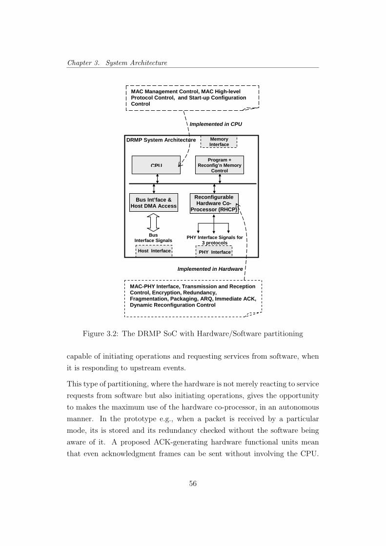
Chapter 3. System Architecture
PHY Interface Host Interface
Memory Interface
Bus Int’face & Host DMA Access
CPU
ReconfigurableHardware Co-
Processor (RHCP)
Program + Reconfig’n Memory
Control
Bus Interface Signals
PHY Interface Signals for
3 protocols
DRMP System Architecture
MAC Management Control, MAC High-level Protocol Control, and Start-up Configuration Control
MAC-PHY Interface, Transmission and Reception Control, Encryption, Redundancy, Fragmentation, Packaging, ARQ, Immediate ACK, Dynamic Reconfiguration Control
Implemented in Hardware
Implemented in CPU
Figure 3.2: The DRMP SoC with Hardware/Software partitioning
capable of initiating operations and requesting services from software, when
it is responding to upstream events.
This type of partitioning, where the hardware is not merely reacting to service
requests from software but also initiating operations, gives the opportunity
to makes the maximum use of the hardware co-processor, in an autonomous
manner. In the prototype e.g., when a packet is received by a particular
mode, its is stored and its redundancy checked without the software being
aware of it. A proposed ACK-generating hardware functional units mean
that even acknowledgment frames can be sent without involving the CPU.
56
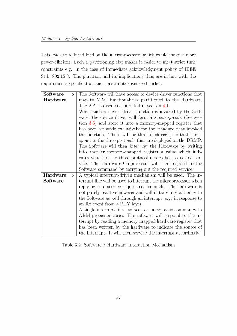
Chapter 3. System Architecture
This leads to reduced load on the microprocessor, which would make it more
power-efficient. Such a partitioning also makes it easier to meet strict time
constraints e.g. in the case of Immediate acknowledgment policy of IEEE
Std. 802.15.3. The partition and its implications thus are in-line with the
requirements specification and constraints discussed earlier.
Software ⇒Hardware
The Software will have access to device driver functions thatmap to MAC functionalities partitioned to the Hardware.The API is discussed in detail in section 4.1.When such a device driver function is invoked by the Soft-ware, the device driver will form a super-op-code (See sec-tion 3.6) and store it into a memory-mapped register thathas been set aside exclusively for the standard that invokedthe function. There will be three such registers that corre-spond to the three protocols that are deployed on the DRMP.The Software will then interrupt the Hardware by writinginto another memory-mapped register a value which indi-cates which of the three protocol modes has requested ser-vice. The Hardware Co-processor will then respond to theSoftware command by carrying out the required service.
Hardware ⇒Software
A typical interrupt-driven mechanism will be used. The in-terrupt line will be used to interrupt the microprocessor whenreplying to a service request earlier made. The hardware isnot purely reactive however and will initiate interaction withthe Software as well through an interrupt, e.g. in response toan Rx event from a PHY layer.A single interrupt line has been assumed, as is common withARM processor cores. The software will respond to the in-terrupt by reading a memory-mapped hardware register thathas been written by the hardware to indicate the source ofthe interrupt. It will then service the interrupt accordingly.
Table 3.2: Software / Hardware Interaction Mechanism
57
Chapter 3. System Architecture
3.6 The Reconfigurable Hardware Co-processor
The Reconfigurable Hardware Co-Processor (RHCP) provides service to up
to three protocol modes concurrently. It implements power-intensive and/or
time-critical tasks. The protocol control of the three protocol modes runs in
the CPU in an interrupt-driven manner (as explained in chapter 4). Each
mode can request service from the RHCP through the use of appropriate API
functions. The RHCP is capable of accepting multiple requests from different
protocol modes, reconfiguring its functional units on the fly as required.
Fig. 3.3 shows the RHCP’s block diagram. Its key design features follow,
after which these features will be discussed in more detail.
Main Features
• The RHCP interacts with the CPU through an Interface and Recon-
figuration Controller (IRC) which delegates tasks to flexible functional
units.
• To optimize power-efficiency, the RHCP has coarse-grained, heteroge-
neous, function-specific Reconfigurable Functional Units (RFUs).
• These RFUs have a standardized interface.
• They are dynamically and individually reconfigurable.
• They are connected by a single packet bus that also connects them to
the packet-memory and the IRC.
• Communication between the RFUs is primarily through the memory,
although the architecture supports direct peer-to-peer communication
between RFUs as well.
• A separate memory holds configuration data for the RFUs and has its
own access buses.
58

Chapter 3. System Architecture
Bus Req/Grnt
Bus Signals
Bus Signals
RFU Pool
RFU1
RFU2
RFUn Bus Signals
Interface &Reconf’n Controller
(IRC)
BufferMode A
BufferMode B
BufferMode C
Event Handler
Interface to PHY
Interface to Microprocessing Unit (MPU)
Pack
et B
us A
rbite
rR
econ
f’n B
us A
rbite
r
Pack
et M
emor
yR
econ
f’n M
emor
y
Interrupt Control InputMPU’s Direct Access to Packet Memory
Packet Bus
Reconf’n Bus
Bus Signals
Upstream Arbiter
Trigger Control Other
Control
Figure 3.3: The Reconfigurable Hardware Co-processor
• Both the reconfiguration and the packet buses can be mastered by any
RFU or the IRC, and hence access to them is arbitered.
• An Event handler interprets Rx events and formats service requests for
the IRC.
• Buffers at the boundary between the MAC layer and the PHY layer
59

Chapter 3. System Architecture
translate between: 32 bit data words of the architecture and data width
required by the PHY (e.g. byte-wide in case of WiFi); and architecture
frequency and protocol frequency.
3.6.1 The Interface and Reconfiguration Controller
The Interface and Reconfiguration Controller (IRC) of the RHCP is a key
innovation of the architecture. An Interface Controller (IC) interprets CPU
commands to the RHCP, and delegates them to RFUs. A complementary
Reconfiguration Controller (RC) controls reconfiguration of the RFUs dy-
namically. The IRC controls packet to packet configuration switch in the
RHCP, and delegates tasks to the RFUs.
3.6.1.1 Structure of the IRC
The IRC is a combination of interacting controllers. At its top level (Fig. 3.4),
it has an Interface Controller and a Reconfiguration Controller. The IC
has two interface modules: one that receives the service requests from the
CPU, and the other that interrupts the MPU. The control task of the IC is
delegated to three Task Handlers (TH), one for each of the three protocol
modes that are running concurrently. Each of these task handlers is composed
of a task-handler for reconfiguration (TH R), and a task-handler for MAC
operations (TH M). These seven controllers work concurrently and, through
a combination look-up tables and mutex registers, implicit control of shared
resources is maintained. There is no single master controller.
The Look-up Tables: The IRC maintains two tables, one static and the
other dynamic, to interpret and respond to service requests. The first, static
table is the op code table (Table 3.3). For each op-code, it has a field for
the RFU and its configuration state which that op-code corresponds to. The
other, dynamic table is the rfu table (Table 3.4) that maintains the status
of the RFUs. This table has a number of fields for each RFU indicating
whether the RFU is in use, the current configuration state of the RFU, and
60

Chapter 3. System Architecture
In Interface
GenerateInterrupt
Task Handler A
Reconf’n MAC
Task Handler B
Reconf’n MAC
Task Handler C
Reconf’n MAC
Interface C ontroller
Rec
onfi
gura
tion
Con
trol
ler
Op-Codetable
RFU-table
Arbiter
Arbiter
Handshake Signals
MPU Interface
Bus Requests
Bus Grants/ ‘Done’ from RFUs
PacketBus
Reconf’nBus
Figure 3.4: The Interface and Reconfiguration Controller
the status of any queued requests for that RFU. The output from the tables
is compatible with the 32-bit hardware architecture.
The op code table can be hardwired at fabrication time, but in the interest
of future-proofing the architecture, it would be best implemented in Flash /
Electrically Erasable Programmable Read-Only Memory (EEPROM) so the
it can be updated by a designer at compile time.
The rfu table on the other hand is a dynamic table and needs to be in
a Random-access memory (RAM). It is quite possible to implement it as
a memory-resident data structure in the packet memory. I have chosen to
model it as a separate physical memory in the prototype. The reason is that
the main data memory (i.e. the packet memory and the associated packet -
bus is already a contentious resource7, with the IRC and the RFUs vying for
access, and having to wait while another protocol mode uses them. Having a
7Refer to section 5.5 where the interconnect bottleneck is discussed.
61

Chapter 3. System Architecture
separate physical memory for the rfu table (in close proximity to the IRC)
allows one protocol mode to look up the tables and carry on operations in
its task handler, while another protocol mode may concurrently be using
the packet memory to carry out its tasks.
Table 3.3: The op code table
Field Size(bits)
Number of Pos-sible Values
Description
op code (Key) 8 256 Tells IRC which service is re-quested.
nargs 4 16 The number of argumentsthat need to be passed to therelevant RFU to execute theop code
rfu id 8 256 Identity of the RFU that cor-responds to this op code.
reconf state 4 16 The configuration state inwhich the RFU should be toexecute this op code.
config vector 2 4K The relative address for load-ing configuration data. Notused in prototype.
3.6.1.2 Functionality of the IRC
A request for service from the software triggers a series of RFUs to execute
their task, but not before they are reconfigured for that particular task.
An op-code corresponds to a request for service from an RFU in a particular
reconfiguration state. One software request may consist of multiple op-codes,
and hence the request may be termed a super -op-code. A super-op-code
request initiates a sequence of operations in the IRC. Its interface module
receives the request and passes it on to one of the three task handlers. The
TH R cycles through the op-codes in the super-op-code, looking up the op -
code table and rfu table for each op-code. It invokes the RC if an RFU is
in the wrong state. The RC then triggers the RFU and reconfigures it to the
required configuration. As soon as the TH R has cleared the first op-code of
62

Chapter 3. System Architecture
Table 3.4: The rfu tableField Size
(bits)Number of Pos-sible Values
Description
rfu id (Key) 8 256 Identity of RFU. Key for thetable.
c state 4 16 The current state of the RFU.A value of 0 indicates RFUhas not been initialized.
nstates 4 16 Number of different valid con-figuration states for the RFU.
in use 1 2 Indicates whether RFU is freeor in use.
Qreq1 2 4 Indicates which first protocolmode has a request queuedfor this RFU. 0 indicates nopending requests. (Two re-quests can be queued, servedon a first-come first-served ba-sis in the prototype).
PrQreq1 2 4 Indicates the priority of re-quest 1. Not used in the pro-totype. See description forQreq1.
Qreq2 2 4 Indicates which second proto-col mode has a request queuedfor this RFU.
PrQreq2 2 4 Indicates the priority of re-quest 2. Not used in the pro-totype.
the super-op-code, it triggers the corresponding TH M. The TH M then reads
the op-code and the associated arguments, interprets the op-code command
using the op-code table, passes arguments to the RFUs and triggers them.
Fig. 3.5 is a Unified Modeling Language (UML) statechart diagram of a
Task-handler for Reconfiguration, and Fig. 3.6 is a UML statechart diagram
of a Task-handler for MAC. It can be seen that they go through a sequence
63

Chapter 3. System Architecture
of states that correspond to using a particular resource or waiting for a
resource to become free. The TH R, after having checked and—if required—
configured the first RFU needed to service the request from MPU, triggers
its corresponding TH M to indicate it can start.
WAIT4_OCT
GO / Read Service Request Op-code
WAIT4_RFUT
[OCT is Free] / Read OCT
[RFUT is Free] / Read RFUT
SLEEP[RFU in use by other mode] / Queue in RFUT
USE_RFUT1WAKE
WAIT4_RC
USE_RC_WAIT
[RC is free]
Trigger RC toreconfigure RFU;wait for confirmation
Update RFUTable 'in_use';Check its state
WAIT4_RFUT2
RC_DONE
USE_RFUT2
[RFUT is Free]
[More op-codes in Service Request]
Wait forOp-code tableto be free
Wait forRFU tableto be free
Wait for Reconf'nController to become available
TRANSITION KEY---------------------
[ Guard condition ] / Transition Action Event / Transition Action
ACRONYMS--------------
RFU --> Reconfigurable Functional UnitRFUT --> RFU TableOCT --> Op-code TableRC --> Reconfiguration ControllerTH_M --> Task Handler for MACTH_R --> Task Handler for Reconfiguration
GO: Event from' In Interface'indicating a service request
IDLE
[RFU already in required config. state]
/ Read Next Op-Code
Figure 3.5: Statechart of Task-handler for Reconfiguration
64

Chapter 3. System Architecture
WAIT4_OCT
GO TH_M / Read Service Request Op-code
WAIT4_RFUT
[OCT is Free] / Read OCT
[RFUT is Free] / Read RFUT
SLEEP2[RFU in use by other mode] / Queue in RFUT
SLEEP1[RFU in use by same mode's TH_R]
TICK
USE_RFUT1WAKE
WAIT4_PBUS
USE_PBUSUse Packet Bus to pass Arguments to RFU
Update RFUTable 'in_use'
WAIT4_RFUDONE
WAIT4_RFUT2
[RFU indicates its done]
USE_RFUT2
[RFUT is Free]
/ Send WAKE if required
[More op-codes in Service Request] / Read Next Op-code
Wait while RFU completes its assigned Task
Wait forOp-code tableto be free
Wait forRFU tableto be free
Wait for Packet bus to become available
GO TH_M: Eventfrom TH_R indicatingfirst RFU is ready
IDLE
TRANSITION KEY---------------------
[ Guard condition ] / Transition Action Event / Transition Action
ACRONYMS--------------
RFU --> Reconfigurable Functional UnitRFUT --> RFU TableOCT --> Op-code TablePBUS --> Packet BusTH_M --> Task Handler for MACTH_R --> Task Handler for Reconfiguration
Figure 3.6: Statechart of Task-handler for MAC Operations
We will look into the operation of the TH M in a little more detail, since it
explains how shared resources are used amongst the three protocols. The
65
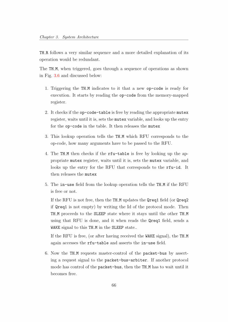
Chapter 3. System Architecture
TH R follows a very similar sequence and a more detailed explanation of its
operation would be redundant.
The TH M, when triggered, goes through a sequence of operations as shown
in Fig. 3.6 and discussed below:
1. Triggering the TH M indicates to it that a new op-code is ready for
execution. It starts by reading the op-code from the memory-mapped
register.
2. It checks if the op-code-table is free by reading the appropriate mutex
register, waits until it is, sets the mutex variable, and looks up the entry
for the op-code in the table. It then releases the mutex
3. This lookup operation tells the TH M which RFU corresponds to the
op-code, how many arguments have to be passed to the RFU.
4. The TH M then checks if the rfu-table is free by looking up the ap-
propriate mutex register, waits until it is, sets the mutex variable, and
looks up the entry for the RFU that corresponds to the rfu-id. It
then releases the mutex
5. The in-use field from the lookup operation tells the TH M if the RFU
is free or not.
If the RFU is not free, then the TH M updates the Qreq1 field (or Qreq2
if Qreq1 is not empty) by writing the Id of the protocol mode. Then
TH M proceeds to the SLEEP state where it stays until the other TH M
using that RFU is done, and it when reads the Qreq1 field, sends a
WAKE signal to this TH M in the SLEEP state..
If the RFU is free, (or after having received the WAKE signal), the TH M
again accesses the rfu-table and asserts the in-use field.
6. Now the TH M requests master-control of the packet-bus by assert-
ing a request signal to the packet-bus-arbiter. If another protocol
mode has control of the packet-bus, then the TH M has to wait until it
becomes free.
66
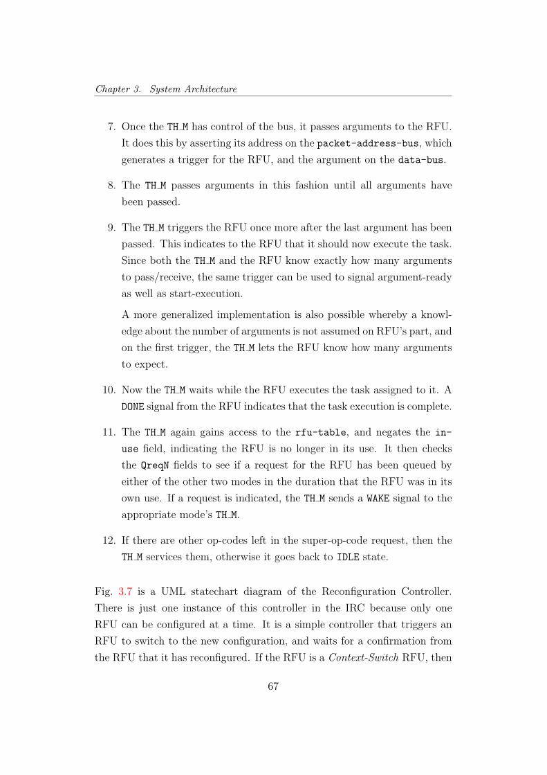
Chapter 3. System Architecture
7. Once the TH M has control of the bus, it passes arguments to the RFU.
It does this by asserting its address on the packet-address-bus, which
generates a trigger for the RFU, and the argument on the data-bus.
8. The TH M passes arguments in this fashion until all arguments have
been passed.
9. The TH M triggers the RFU once more after the last argument has been
passed. This indicates to the RFU that it should now execute the task.
Since both the TH M and the RFU know exactly how many arguments
to pass/receive, the same trigger can be used to signal argument-ready
as well as start-execution.
A more generalized implementation is also possible whereby a knowl-
edge about the number of arguments is not assumed on RFU’s part, and
on the first trigger, the TH M lets the RFU know how many arguments
to expect.
10. Now the TH M waits while the RFU executes the task assigned to it. A
DONE signal from the RFU indicates that the task execution is complete.
11. The TH M again gains access to the rfu-table, and negates the in-
use field, indicating the RFU is no longer in its use. It then checks
the QreqN fields to see if a request for the RFU has been queued by
either of the other two modes in the duration that the RFU was in its
own use. If a request is indicated, the TH M sends a WAKE signal to the
appropriate mode’s TH M.
12. If there are other op-codes left in the super-op-code request, then the
TH M services them, otherwise it goes back to IDLE state.
Fig. 3.7 is a UML statechart diagram of the Reconfiguration Controller.
There is just one instance of this controller in the IRC because only one
RFU can be configured at a time. It is a simple controller that triggers an
RFU to switch to the new configuration, and waits for a confirmation from
the RFU that it has reconfigured. If the RFU is a Context-Switch RFU, then
67

Chapter 3. System Architecture
the reconfiguration is done just by the act of switching to a new context. If
it is a Memory-Access RFU—an RFU that reads configuration data from
memory on a mode-switch— then the RFU reads configuration data and lets
the RC know when it is done. The reconfiguration mechanism of an RFU is
transparent to the RC.
WAIT4_OCT
REC_REQ
TRIGGER_RCNFG_WAIT
[OCT is free] / Use OCT
WAIT4_RFUT
RFU_RDONE
UPDATE_RFUT
[RFUT is free]
/ RC_DONE
Trigger RFUreconfiguration;wait until its done
Update RFUTto indicateRFU's new state
TRANSITION KEY---------------------
[ Guard condition ] / Transition Action Event / Transition Action
ACRONYMS--------------
REC_REQ --> Event from TH requesting ReconfigurationRFUT --> RFU TableOCT --> Op-code TableRFU_RDONE --> Event from RFU: reconf'n completedRC_DONE --> Event to TH: reconf'n completed
Figure 3.7: Statechart of Reconfiguration Controller
3.6.2 The Reconfigurable Functional Units
The DRMP has a pool of RFUs (Fig. 3.3). They have a uniform interface and
are responsible for carrying out the tasks requested by the CPU. The RFUs
are heterogeneous and dynamically as well as individually reconfigurable.
The functionality of the different specialized RFUs is derived from the study
of different wireless standards to see the type of operations typically carried
out.
That the RFUs are heterogeneous, coarse-grained, and function-specific—
catering to a particular domain—is what sets the DRMP apart from other
68
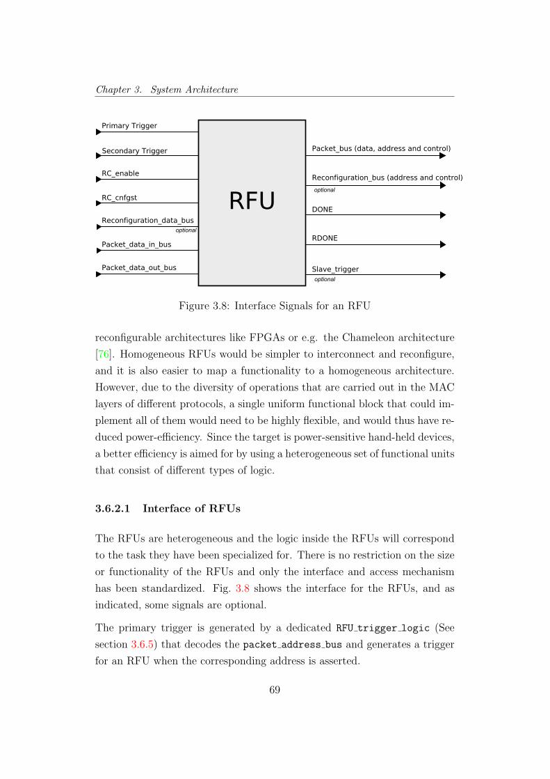
Chapter 3. System Architecture
RFU
Primary Trigger
Secondary Trigger
RC_enable
RC_cnfgst
Reconfiguration_data_bus
Packet_data_in_bus
Packet_data_out_bus
Packet_bus (data, address and control)
Reconfiguration_bus (address and control)
DONE
RDONEoptional
optional
Slave_triggeroptional
Figure 3.8: Interface Signals for an RFU
reconfigurable architectures like FPGAs or e.g. the Chameleon architecture
[76]. Homogeneous RFUs would be simpler to interconnect and reconfigure,
and it is also easier to map a functionality to a homogeneous architecture.
However, due to the diversity of operations that are carried out in the MAC
layers of different protocols, a single uniform functional block that could im-
plement all of them would need to be highly flexible, and would thus have re-
duced power-efficiency. Since the target is power-sensitive hand-held devices,
a better efficiency is aimed for by using a heterogeneous set of functional units
that consist of different types of logic.
3.6.2.1 Interface of RFUs
The RFUs are heterogeneous and the logic inside the RFUs will correspond
to the task they have been specialized for. There is no restriction on the size
or functionality of the RFUs and only the interface and access mechanism
has been standardized. Fig. 3.8 shows the interface for the RFUs, and as
indicated, some signals are optional.
The primary trigger is generated by a dedicated RFU trigger logic (See
section 3.6.5) that decodes the packet address bus and generates a trigger
for an RFU when the corresponding address is asserted.
69

Chapter 3. System Architecture
There is an optional secondary trigger that comes into play when RFUs
directly access one another in a master-slave fashion (see section 3.6.5).
The RC en (Reconfiguration enable) and RC cnfgst (Reconfiguration state)
signals are used by the Reconfiguration Controller to configure the RFUs.
(See section 3.6.2.2)
The Memory-Access RFUs have the reconfiguration data bus as input to
read configuration data, and can assert the reconfiguration address bus.
All RFUs can write on the packet address bus and the packet data in -
bus. Since RFUs can both write to, and be written to, on the packet bus,
both the packet data out bus and the packet data in bus (latched) are
inputs to the RFUs. (See section 3.6.3).
Although there is a separate packet data out bus and packet data in -
bus in the prototype model, they can implemented as single multiplexed bi-
directional packet bus, which would result in reduced interconnect overhead.
All RFUS have a DONE signal to indicate that they have finished the task
assigned to them, and an RDONE signal to indicate that they have reconfigured
(See section 3.6.2.1).
3.6.2.2 Reconfiguration of RFUs
The RFUs in the DRMP are function-specific, and the degree of flexibility
required by an RFU will vary. This would depend on the extent of similarity
of functionality between the different protocol standards that use that RFU.
Some RFUs may be quite general-purpose having LUTS. Some RFUs may
be slightly flexible by changing some parameters, and some RFUs could be
configured simply by changing a control signal.
In general, the RFUs are meant to be function-specific with limited flexibility,
and this leads to power-efficient reconfiguration because they need relatively
less configuration data when compared with general purpose configurable
logic blocks based on look-up tables.
While there is a central Reconfiguration Controller (part of the IRC)
70

Chapter 3. System Architecture
that gives the commands to the RFUs to configure to a certain mode, the
RFUs carry out their own configuration and signal the IRC when they are
done by asserting the RDONE signal. The actual reconfiguration mechanism
can be one of two, and is transparent to the Reconfiguration Controller.
The RFUs can be reconfigured either by a context-switching mechanism
(Context-Switching RFUs or CS-RFUs) or by loading configuration data
from a memory, i.e Memory-Access RFUs (MA-RFUs).
The memory access mechanism allows RFUs to access configuration data
autonomously through the dedicated reconfiguration bus and reconfig-
uration memory. This will result in the overhead of control logic needed by
an RFU to generate signals for the reconfiguration bus. The RFUs will
store configuration vectors in local registers that will be loaded at startup. It
is also possible to pass these configuration vectors as arguments by the IRC.
This overhead of control logic in each RFU for configuration memory ac-
cess can be minimized through means of an intermediate Memory manager
module. E.g. it could abstract the interface of the associative reconfigura-
tion memory and present a simple stack interface to the RFU. The memory-
manager could be configured at startup, and during operation, the RFUs
could simply pop reconfiguration data from the memory.
RFUs implementing the context-switching reconfiguration mechanism will be
configured simply by switching the control signal RC cnfgst. The RFU will
still respond by asserting the RDONE signal, albeit much quicker (in 1-2 clock
cycles) than an MA-RFU would. Note though that to the IRC’s reconfiguration
controller, the reconfiguration mechanism will remain transparent. It will still
reconfigure the RFU through a combination of RC cnfgst and RC en signals,
and wait for the RDONE signal from the RFU.
By default, RFUs will be assumed to be MA-RFU, unless one or more of the
following apply, in which case they would be implemented as a CS-RFU:
• Small RFUS for which the reconfiguration memory access overhead
may become relatively large.
71

Chapter 3. System Architecture
• Time-critical RFUs for which little time is available to reconfigure.
• For RFUs where there is little reconfiguration data, it may be more
power-efficient to store the data as on-chip contexts at start-up, rather
than initiate a memory access mechanism just for the sake of transfer-
ring e.g. a few bytes of configuration data.
3.6.2.3 RFU Partitioning
The DRMP architecture leaves the door open for incorporating a variety
of functionality, flexibility and granularity of RFUs. The choice of RFUs
is in itself an interesting investigation, and will depend on the domain tar-
geted, as well as the requirements of flexibility vs. power efficiency8. In
general, the RFUs in the DRMP are meant to be function-specific, flexible,
and coarse-grained. While the architecture on the whole is reconfigurable,
the RFUs may be better termed as parameterizable since they are expected
to be heterogeneous and function-specific, with small variations allowed to
make them work for different protocol standards. Rabaey [72] also proposes
parameterizable functional units, though not in a MAC-layer context.
As for choosing the functionality and granularity of RFUs, two possible ap-
proaches were considered:
1. Identifying the design space, simulating benchmark applications on all
the design points and then judging the outcomes based on specified
metrics of power-efficiency [1]. Though this approach does have a
clear optimization advantage, it is a very time-consuming task—a re-
search avenue of its own. It was not deemed a suitable expenditure of
research effort since it would have shifted focus away from the archi-
tecture modeling at a system level.
2. The other approach, chosen for the DRMP architecture design, is a
heuristic, relatively less formal approach. I looked at overlaps in differ-
ent wireless MACs, and studied other publications discussing Hardware
8In section 4.3, this trade-off is discussed in context of a platform DRMP architecture.
72

Chapter 3. System Architecture
/ Software partitioned MAC implementations [65, 85, 77, 28, 62]. Then
the following steps lead to a suitable choice of RFUs:
(a) Start with the assumption that the more coarse-grained an RFU
the better it is for the power-efficiency. The more fine-grained an
architecture is, the more will be the routing area overhead [29].
(b) In the first iteration, the focus was on functional blocks that would
be needed to implement a WiFi MAC9. Though prior research was
investigated to identify functions that need hardware acceleration,
the granularity was set by the criteria that an RFU will be as
coarse-grained as possible. The limiting factor would be that it
should carry out its complete task in response to a single service
request from the software implemented protocol state machine.
An RFU should not have to stop in the middle of its operation
to wait for an update from the protocol control. The criteria is
important because the RFUs are shared between three concurrent
protocols modes. Holding an RFU without using it, while CPU
carries out protocol control operations, is not a feasible solution.
(c) After this first, WiFi oriented, ‘seed’ partitioning of the RFUs, the
second and then the third protocol are introduced. The guiding
criteria being that an existing RFU is broken down into (two or
more) smaller RFUs in the situation where the only way to reuse
the resources of that RFU is to break it down into smaller RFUs,
one or more of which can be re-used for the other protocols. If a
functionality is encountered that is entirely new, then a new RFU
9WiFi has been chosen as the baseline protocol for the sake of convenience. It ispossible that taking the other protocols as baseline would lead to a better partitioning.E.g. consider a protocol that is investigated at the end of this partitioning exercise, anda new RFU is added for a functionality needed by it. If that protocol would have beenconsidered earlier, it is quite possible that this RFU would have been deemed suitablefor re-use by another protocol considered afterward, perhaps by partitioning it into twosmaller RFUs.
This potential snag in the approach can be overcome by doing a second iteration afterpartitioning result of the first round. This second iteration would look at the RFUs addedfor the protocols other than the baseline protocol, and investigate if any of these RFUscan be re-used, as-is or broken down, for another protocol.
73

Chapter 3. System Architecture
is added based on the criteria in step (b).
(d) For future-proofing, flexible, general-purpose RFUs may be added.
This aspect is discussed in section 4.3
Taking this approach will yield a suitable set of RFUs for the DRMP. It is a
top-down approach, starting from coarse-grained RFUs and breaking them
into smaller units only when needed. Since DRMP addresses power-sensitive
devices, such an approach will result in a near-optimal solution in context.
3.6.3 Memories and Interconnect
The RHCP needs data storage for two main purposes: First, to store and
work with packet data, and its intermediate forms. Note that packet data
of three different modes need to be available. Second, to store configuration
data for the RFUs.
A number of possibilities for the memory architecture exist:
1. Single memory for all modes’ configuration and packet data. (1 mem-
ory)
2. Separate physical memory for each mode. (3 memories)
3. Separate physical memory for configuration data and for packet data.
(2 memories)
4. Separate physical memory for each mode’s configuration data and packet
data. (6 memories)
The advantages and disadvantages of these options are discussed in Table 3.5.
I have chosen option 3. This gives two advantages: It allows concurrent
operation on the configuration data and the packet data. Hence one RFU
can configure itself while another RFU carries out operation on the packet
74

Chapter 3. System Architecture
data. It also implies that one can optimize each memory according to its
requirement.
The packet-memory is modeled as a dual-port memory so that one port can
be dedicated to the CPU which needs to access packet data to carry out
its control operation. Hence, while one mode may be accessing packet-data
in the RHCP (e.g. RFU carrying out encryption), another mode may be
reading header data and carrying out control operations through the CPU.
Fig. 3.9 shows a tentative memory-map of the packet-memory. The interface
registers for communicating data and control information between the RHCP
and CPU are mapped to the packet-memory. And while the lookup tables in
the IRC are presently modeled as separate physical memories inside the IRC
(again, to allow one mode to carry out control operations in the IRC which
requires accessing the lookup tables, while another mode to concurrently
access packet data through an RFU), it is also possible to map these tables
to the packet-memory. This will save area and power, and with the time-
slack available (see section 5.4), it may be the more appropriate option. One
address from the packet-memory is mapped to each RFU and is used to
address an RFU to pass arguments or trigger it.
Packet data of various modes is stored in pages to minimize address-house-
keeping; making use of the fact that packet-data in the packet-memory will be
stored and retrieved in predictable patterns. This is true because at any one
time, for one protocol, only one packet will be stored in the packet-memory,
in the process of being transmitted or received. Buffering of packets will be
done in transmit and receive First In, First Out Memories (FIFOs). Due
to protocol constraints, one can easily fix the maximum size the a packet-
data of a protocol can take at any time. Thus one can fix page-sizes for
packet-data in the memory for the worst-case scenario (largest packet size),
with each page corresponding to a certain stage the data is in while it is
being processed, e.g. post-fragmentation, post-encryption etc. The starting
address of packet-data at various stages is hence completely fixed, and the
RHCP’s IRC or the CPU are relieved from any memory-management tasks.
E.g. the starting address of data to be encrypted for protocol A will always
75
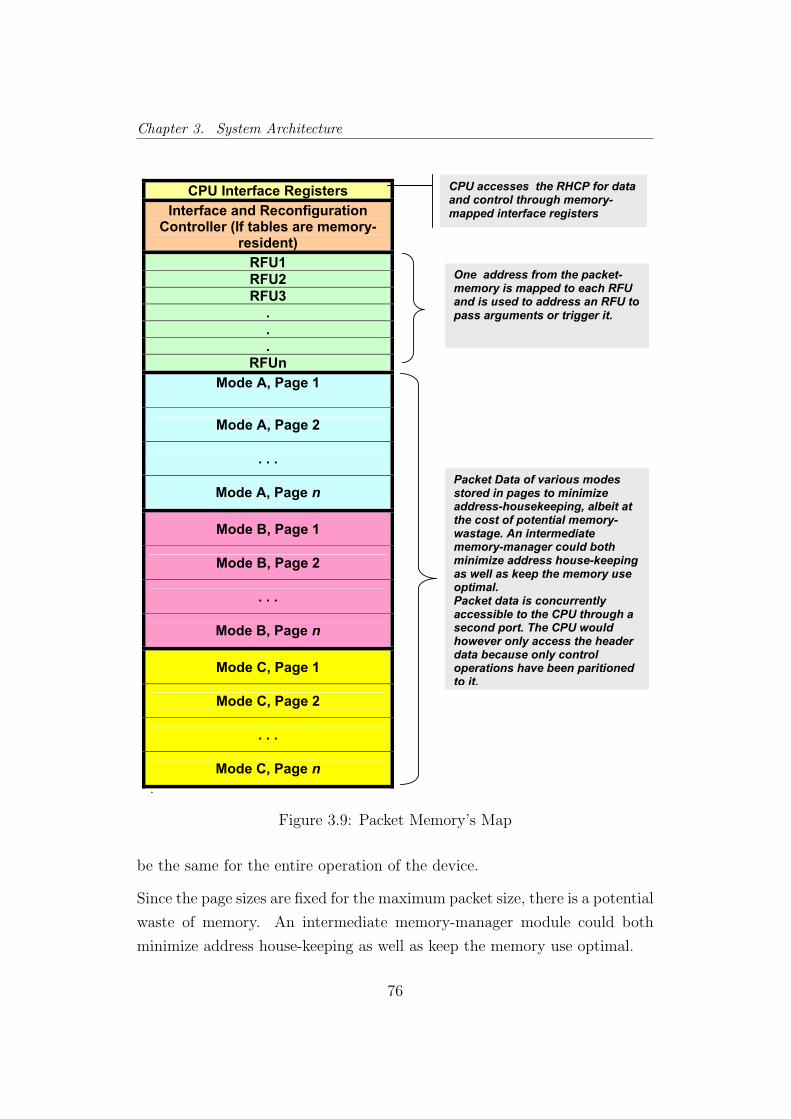
Chapter 3. System Architecture
Packet Data of various modes stored in pages to minimize address-housekeeping, albeit at the cost of potential memory-wastage. An intermediate memory-manager could both minimize address house-keeping as well as keep the memory use optimal. Packet data is concurrently accessible to the CPU through a second port. The CPU would however only access the header data because only control operations have been paritioned to it.
One address from the packet-memory is mapped to each RFU and is used to address an RFU to pass arguments or trigger it.
`
CPU Interface Registers Interface and Reconfiguration
Controller (If tables are memory-resident)
RFU1 RFU2 RFU3
.
.
. RFUn
Mode A, Page 1
Mode A, Page 2
. . .
Mode A, Page n
Mode B, Page 1
Mode B, Page 2
. . .
Mode B, Page n
Mode C, Page 1
Mode C, Page 2
. . .
Mode C, Page n
CPU accesses the RHCP for data and control through memory-mapped interface registers
Figure 3.9: Packet Memory’s Map
be the same for the entire operation of the device.
Since the page sizes are fixed for the maximum packet size, there is a potential
waste of memory. An intermediate memory-manager module could both
minimize address house-keeping as well as keep the memory use optimal.
76
Chapter 3. System Architecture
Packet data is concurrently accessible to the CPU through a second port.
The CPU would however only access the header data because only control
operations have been partitioned to it.
In terms of interconnect requirements, all RFUs need to be accessible by the
IRC. All RFUs also need read and write access to the packet memory. The
MA-RFUs will also need read access to the config memory to read config-
uration data. Direct, peer-to-peer communication should also be possible
amongst the RFUs, even though the RFUs primarily communicate through
the memory.
It is important to point out here that the RHCP reconfigures packet-to-packet.
This means that at any one time, the RHCP is catering to the MAC functions
of any one mode. Although it is quite straightforward to extend the archi-
tecture’s features to include true concurrent operations of multiple modes in
the hardware co-processor, in view of the time-slack (See section 5.5) and
the requirements for power-efficiency, such an approach was considered an
overkill. Hence it was decided that there was no need to provide for concur-
rent processing of packet data on the RHCP. With this in mind, the most
straightforward communication architecture was a simple bus-based archi-
tecture that provided full-connectivity, shared through time-multiplexing by
multiple modes. As a result though, the interconnect becomes the bottleneck
for the performance/throughput as well, as discussed in section 5.5.
The RFUs are all connected via a single-bus network that also connects
them to the packet memory. They are each assigned an address, and an
address decoder translates write operation to these addresses into triggers
for the RFUs. An interesting aspect of the architecture is that the IRC or
any of the RFUs can become a master of the packet-bus. A bus arbitration
block manages the multiple potential masters for the buses. Hence the same
packet-bus can be used for:
• The IRC writing data to RFU,
• The IRC writing data to the packet memory,
77

Chapter 3. System Architecture
• An RFU writing data to the packet memory or
• An RFU writing data to another RFU.
A separate configuration memory has been designed in the RHCP, and a
separate connection route is available to this memory. This allows one RFU
to carry out its reconfiguration while another carries out its MAC task, as
has been discussed in the operation of the IRC in section 3.6.1. It is worth
pointing out that while the packet memory and bus is 32-bits wide in the
prototype, there is no reason why the reconfiguration memory and bus
be the same. There is not enough information at this point to evaluate
the configuration data throughput requirement, but considering the limited
configuration data required by the function-specific RFUs, it is quite likely
that a 16-bit or even a byte-wide configuration may be sufficient to provide
the required configuration throughput at 200 MHz, the clock frequency at
which the prototype architecture model is simulated. A reduced interconnect
is also in-line with the requirements of optimizing power-efficiency for this
architecture.
In section 5.5, it is discussed how the interconnect is the throughput bottle-
neck, because of which a time-multiplex sharing of RFUs has to be enforced.
While a single-bus network has been shown (see section 5.4) to be enough
for 3 concurrent protocol modes with a bandwidth of 20 Mbps at a moderate
clock frequency of 200 MHz, it may become a bottleneck for faster proto-
cols. Increasing clock frequency may not be a feasible option in view of strict
power constraints of hand-held devices. In such a case, other interconnect
options may also be considered. One could simply increase the bus-width
for higher throughput. A multi-bus network [100] may be used to allow two
or three RFUs to simultaneously function for different protocol modes. A
segmented bus [100] could also achieve similar results, with lower resources
but with some additional control operations involved.
Fig. 3.3 which is a block diagram of the RHCP shows how the IRC, the
memories, and the RFU pool are interconnected. Fig. 3.10 goes inside the
RFU pool to show the interconnect between the RFUs and with the IRC (IRC
78

Chapter 3. System Architecture
RFU_1
RFU_2
RFU_3
RFU_n
Reconf’nBus
Arbiter
PacketBus
Arbiter
DONE / RDONE signalsTo IRC
Address, Data and Control to
packet_memory
PHY Interface signals
Bus Request / Grant signalsFrom / to IRC
Address, Data and Control to
reconf’n_memory
Packet_data_bus
Reconfiguration_data_bus
Control Signals from IRCTrigger, Reconf’n trigger and state
Packet_bus signals
From RFUs
Reconf’n_bus signals
From RFUs
Master / SlaveTrigger
Figure 3.10: Connection between the RFUs
79

Chapter 3. System Architecture
block not shown). Note that neither of these figures represent the expected
topology of the components in silicon, but represent the logical layout of the
components and the interconnect.
All RFUs are fed by the reconfiguration-data-bus and the packet-data-
bus. Control signals from the IRC are also input to all RFUs. These signals
include a trigger for initiating task, and a trigger for initiating reconfigura-
tion, unique for each RFU. A common signal indicates to the relevant RFU
the configuration state it is to switch to.
At the output, each RFU can access the packet-bus and the reconfigura-
tion-bus through arbiters. The arbiters are connected to the IRC through
request / grant signals. Each RFU has a DONE and a RDONE signal going to
the IRC, to indicate the completion of a task or reconfiguration.
It is pertinent to point out that the interconnect network design, while fea-
sible and adequate, is not the result of exhaustive research of interconnect
possibilities and a comparative analysis. Future work could yield better al-
ternatives to the one used in the prototype. E.g. according to [100], a
hierarchical interconnect network delivers the best energy efficiency while
maintaining flexibility for heterogeneous reconfigurable systems.
3.6.4 Arbitration
The presence of three asynchronous task-handlers that can run concurrently,
each having two independent and asynchronous controllers, leads to the pos-
sibility of contention on some shared resources like the look-up tables, the
RFUs and the interconnect. The contention on the tables is handled by using
mutex variables that a task-handler asserts when it is reading a table. The
contention over an RFU is handled by a Sleep/Wake and queuing mechanism,
as discussed in section 3.6.1.
In context of the interconnect, there is no contention on the reconfigu-
ration bus as there is just one Reconfiguration controller and hence there
cannot be multiple over-lapping requests for the reconfiguration bus. The
80

Chapter 3. System Architecture
Bus_Master_1
Bus_Master_2
Bus_Master_3
Bus_Master_n
Bus_out
Selection
MUX
MUX
Bus
Arb
itra
tion
Logic
Bus_Request_M
ode_1
Bus_Request_M
ode_2
Bus_Request_M
ode_3
Bus_Grant
Delayed
Bus_Grant
Override
Bus_Grant
Bus
Gra
nt
Logic
Gra
nt
Overr
ide
Logic
Figure 3.11: Arbiter for the Packet Bus
81

Chapter 3. System Architecture
packet bus however may be requested by any of the three concurrent task -
handlers for an RFU’s use, and hence there is a packet bus arbiter in the
Hardware Co-processor. The structure and functionality can best be under-
stood from its block diagram in Fig. 3.11.
The Bus Arbitration Logic decides which of the bus requests should be served.
In the prototype, mode 1 has the highest priority and mode 3 the lowest, but
this can vary.
The Grant Delay Logic has been introduced because the IRC — which nor-
mally has control of the packet bus and makes the bus request on behalf of
an RFU — needs the bus to trigger the RFU so that it can take control the
bus. The trigger is generated by asserting the address of the RFU on the
packet bus. The Grant Delay Logic delays the updated bus grant signal to
the new RFU until the IRC has triggered that RFU by asserting its address
on the address bus. This logic is shown in Fig. 3.12. The Grant Delay Logic
block detects a change in the input Bus-grant signal (coming from the Bus
Arbitration logic), and then checks if this bus request is from an RFU. If it
is, it waits until that RFU is triggered, before changing the output bus-grant
signal to the new input value. If the request is from the IRC or the bus-grant
signal has been reset, then there is no need to wait and the output is updated
immediately.
The Grant Override Logic is relevant to the master-slave scenario and is
discussed in section 3.6.5.
3.6.5 RFU Trigger Logic and Master-Slave Mechanism
All the RFUs in the RHCP are assigned a unique address (See Fig. 3.9
showing the packet-memory’s map). A trigger-logic module (Fig. 3.13)
decodes this address and generates a trigger if an RFU is addressed on the
packet-bus. In the prototype model, the trigger-logic module looks for
address between a hard-wired range of addresses. It then calculates the ID
of the addressed RFU by calculating the offset of the asserted address from
a known base-address. This works because the RFUs are assigned addresses
82

Chapter 3. System Architecture
IDLE
TRIGGER WAIT
[Change Detected in Input Bus-grant signal]
[Request from an RFU]
/ Bus-grant-out = Bus-grant-in
[Request from IRC ORBus-grant Reset]
[Detect RFU Trigger]
Figure 3.12: Bus Grant Delay Logic
sequentially from a base address in an ascending order of their ID numbers.
In certain situations however, this primary trigger mechanism is not enough.
RFUs typically operate on a block of data (packet/fragment) and then the
IRC hands over control to another RFU. It was observed however that some
RFUs will need to interact with another RFU on every word. Involving the
IRC to switch bus control back and forth between the two RFUs would have
resulted in unnecessary overhead.
Also, although an RFU can directly trigger another RFU by asserting its
address on the packet-address-bus, there arose situations where an RFU
would be reading data from a memory while requiring another RFU to pro-
cess this data10. Since the packet-address-bus is being used by the first
RFU to read the memory, it cannot use the same bus to generate a primary
trigger for another RFU concurrently.
10E.g. in the prototype model, the Transmission RFU, while reading data from thepacket-memory, requires the CRC RFU to read this data too and internally update thechecksum value.
83

Chapter 3. System Architecture
RFU Trigger Logic
RFU_Trigger_1
RFU_Trigger_2
RFU_Trigger_3
RFU_Trigger_n
Write_enable
Packet_address_bus
IDLE
SEND
[Write Enable Asserted]
[Address in RFU Range] / RFU ID = Current Address - RFU Base Address
/ Assert Trigger to RFU
/ Negate Trigger to RFU
(a) RFU Trigger Block Diagram
(b) RFU Trigger Logic
Figure 3.13: RFU Trigger Generation Module
84
Chapter 3. System Architecture
To overcome this problem, the RHCP implements a master / slave mecha-
nism whereby an RFU can become the master of another RFU, triggering it
directly on a secondary trigger (Fig. 3.8) rather than through asserting the
second RFU’s address on the address bus and generating a primary trigger.
Having identified the need to implement a secondary trigger mechanism, the
following design options were considered:
1. Changing the trigger-logic. Storing the address-table in the trigger-
generator in a RAM, and dynamically updating it as required. The
slave RFU would be allocated the address range that the master RFU
intends to access in the packet-memory to read data. In this way,
whenever the master RFU read data from the packet-memory, the
slave RFU would be triggered simultaneously.
2. Having a secondary address-bus that addresses RFUs only. A separate
trigger-generation logic would be needed to decode the addresses and
generate an RFU trigger. The secondary address-bus will need to be
log2N bits wide, where N is the number of RFUs. Since there are
a limited number of coarse-grained RFUs, this bus should be quite
narrow, and certainly less than byte-wide.
3. Hard-wired peer-to-peer trigger lines between potential master-slave
pairs.
These three options are shown in Fig. 3.14. Note that only the signals relevant
to the generation of trigger for a slave RFU are included in this figure. The
complete interconnect is shown in Fig. 3.10
In the current prototype, I have chosen option 3 (Fig. 3.10). This hard-
wired approach has been taken because—the DRMP being a domain-specific
architecture—only a limited number of master-slave pairs were identified. A
more general-purpose secondary trigger mechanism like the other two option
was considered unnecessary overhead.
85

Chapter 3. System Architecture
MasterRFU
PacketMemory
TriggerControl
Slave RFU
Address
Data
Primary Trigger
DynamicAddress LUTUpdates From
IRC
MasterRFU
PacketMemory
TriggerControl
Slave RFU
Data
Primary Trigger
RFU_Address
Address
MasterRFU
PacketMemory
Slave RFU
Address
Data
Secondary Trigger(Peer-to-peer)
(a) IRC Updates Lookup-table so that slave RFU is triggered when Master read from
Memory
(b) Master asserts slave’s address on the secondary ‘RFU_Address’ bus, and Trigger
Control generates trigger for slave
(c) Master directly triggers slave through a dedicated, secondary trigger line (Trigger-logic
not relevant hence not shown)
Used in the prototype DRMP model
Figure 3.14: Different Options Considered to Allow a Master RFU to Con-currently Access Memory and Trigger a Slave RFU
86

Chapter 3. System Architecture
An issue arises here of handing over the bus control to a slave RFU by a
master RFU. Bus grants are normally handled by the IRC, which can assert
the Id of the relevant RFU on a bus request signal to the bus arbiter. A
mechanism was needed for an RFU to hand over bus access to another RFU.
For this purpose, a Bus Grant Override module has been introduced in the
packet bus arbiter (Fig. 3.11). An RFU can override the current bus-grant
(to itself, by the IRC), and grant it to another RFU. It would mean the slave
access mechanism is still transparent to IRC, and it is elegant because only
the RFU that already has access to the bus can override the grant and give
it to another RFU. Hence there is no chance of a contention.
The master-RFU asserts a reserved override-address on the packet-address-
bus, while asserting the Id of the slave RFU on the packet-data-bus. The
grant-override-logic inside the packet-bus-arbiter detects this address
and overrides the current grant signal to the arbiter mux by asserting a new
select signal corresponding the override request. Once the slave has used
the bus, assertion of override-address by it will be detected by the grant-
override-logic which will hand the bus back from the slave-RFU to RFU
that was originally master of the bus.
Note that although the secondary trigger option is a hard-coded mechanism,
the architecture still has the capability for any RFU to transparently request
service of any other RFU, since all RFUs are addressable through the address
bus. Only simultaneous access to a slave RFU and the memory (or two slave
RFUs) is limited by hard-wired mechanism.
By selecting appropriate interface signals (see Fig. 3.8), an RFU by can be
designed to work as:
• Master only (no input secondary trigger),
• Slave only (no primary input trigger and no output trigger)
• Neither master or slave (no input secondary trigger, no primary input
trigger, and no output trigger)
87

Chapter 3. System Architecture
• Both master or slave (all signals present)
3.6.6 Event Handler and Interface Buffers
The Event-handler is a simple block that interprets Rx events (Fig. 3.3). If
a packet is to be received, it formats a service request. A service request to
the IRC can thus originate from the either the CPU or the Event-handler.
The source of the request is transparent to the IRC.
Buffers are needed at the boundary between the MAC layer and the PHY
layer. The DRMP is to work with three concurrent modes, and it manages
this because the Hardware Co-Processor has a high throughput as it works
on 32-bit data words at frequencies higher than required by the protocol.
The interface with the PHY module has to be at protocol frequency however.
The transmission and reception RFUs cannot work at the frequency required
by the protocol because their use is multiplexed between multiple concurrent
protocols. The problem is solved by introducing translational buffers between
the MAC and PHY for each of the three modes. These buffers translate
between 1) 32 bit data words of the architecture and data width required
by the PHY (e.g. byte-wide transfer in case of WiFi); and 2) architecture
frequency and protocol frequency.
Fig. 3.15 shows the control flow of the transmission buffer controller that syn-
chronizes between the interface with the PHY, and the interface to the DRMP
architecture (see Fig. 3.3 for context). The buffer control is implemented as
two asynchronous interacting state-machines. One side of the buffer inter-
acts with the DRMP at the architecture frequency and data width, quickly
carrying out the data transaction and leaving the DRMP free to cater to an-
other concurrent protocol mode. The other side of the buffer interacts with
the PHY, transferring data at the frequency and data-width required by the
protocol.
The interface signals for the PHY layer need some elaboration. Each protocol
will have its unique signals for interface between the PHY and MAC. Two
88

Chapter 3. System Architecture
IDLE
/ Initialize buffer pointer
SEND
ACK
END
[DRMP indicates SOP] / increment PSC
[DRMP sends data] / Store data in Buffer
[DRMP indicates EOP] / increment PFC/ACK data to
DRMP
/ACK EOP to DRMP
IDLE
ACK
BYTE
ACK2
[SPC not equal to PSC] / Tx-Start to PHY
[ACK from PHY]
/ Send Byte to PHY
DECISION
[ACK from PHY]
/ Clear Byte Counter
[Packet Not Complete]
[Bytes left in Word] /Increment Byte Counter
[ACK from PHY]
END
[Packet Complete] / Tx-End to PHY,Increment SPC
TRANSITION KEY---------------------------
[ Guard condition ] / Transition Action
ACRONYMS------------------
SOP --> Start of PacketEOP --> End of PacketPSC --> Packets Started CounterSPC --> Sent Packets CounterPHY --> The Physical LayerDRMP--> The MAC Processor
(a) DRMP-side Control (b) PHY-side Control
Figure 3.15: Transmission Buffer Control
approaches can be taken to implement this interface in the DRMP, as shown
in Fig. 3.16:
1. A general interface to the PHY layer provided by the DRMP. It will be
up to the SoC designer using the DRMP IP to introduce the appropriate
wrapper to interface the PHY signals with the signals available at PHY
interface of the DRMP.
2. General-purpose reconfigurable logic interface to the PHY, programmed
by hardware designer at fabrication time to comply with the expected
89

Chapter 3. System Architecture
DRMP
PHYA
PHYB
PHYC
ProtocolWrapper A
ProtocolWrapper C
ProtocolWrapper B
Generalised Interface Signals
Protocol-Specific Interface Signals
PHY I/F PHY I/F PHY I/F
(a) External Wrapper for PHY Interface Implemented by SoC Designer in Fixed or
Reconfigurable Logic
Fixed or Reconfigurable Logic
DRMP
PHYA
PHYB
PHYC
ProtocolWrapper A
ProtocolWrapper C
ProtocolWrapper B
Generalised Interface Signals
Protocol-Specific Interface Signals
PHY I/F PHY I/F
(b) Internal Wrapper for PHY Interface in Reconfigurable Logic
Reconfigurable Logic
PHY I/F
Figure 3.16: Two Possible Options for Implementing PHY-Interface WrapperLogic
protocols. This approach will offer flexibility, with no separate physical
wrapper module required. On the flip side, overheads of introducing
general-purpose logic will be incurred.
90

Chapter 3. System Architecture
In the DRMP prototype model, I have used the second approach. This
way, the choice of implementing the wrappers in reconfigurable logic (for
flexibility) or fixed logic (for efficiency) is left to the SoC integrator.
91
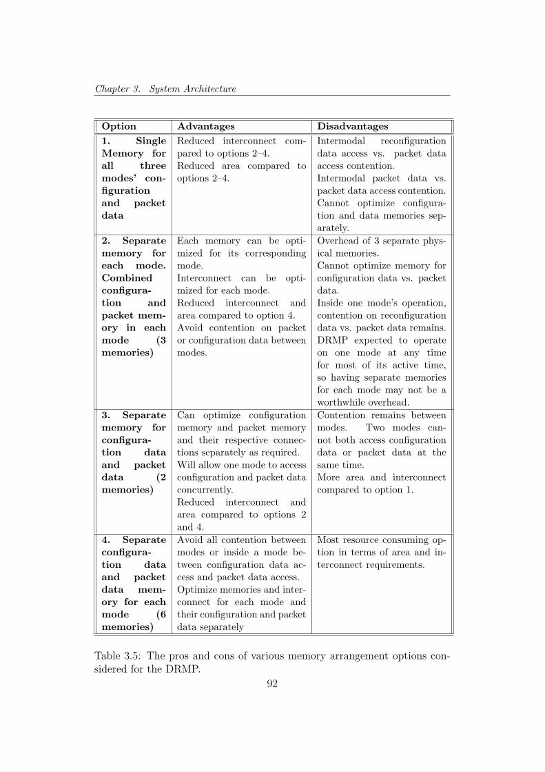
Chapter 3. System Architecture
Option Advantages Disadvantages1. SingleMemory forall threemodes’ con-figurationand packetdata
Reduced interconnect com-pared to options 2–4.Reduced area compared tooptions 2–4.
Intermodal reconfigurationdata access vs. packet dataaccess contention.Intermodal packet data vs.packet data access contention.Cannot optimize configura-tion and data memories sep-arately.
2. Separatememory foreach mode.Combinedconfigura-tion andpacket mem-ory in eachmode (3memories)
Each memory can be opti-mized for its correspondingmode.Interconnect can be opti-mized for each mode.Reduced interconnect andarea compared to option 4.Avoid contention on packetor configuration data betweenmodes.
Overhead of 3 separate phys-ical memories.Cannot optimize memory forconfiguration data vs. packetdata.Inside one mode’s operation,contention on reconfigurationdata vs. packet data remains.DRMP expected to operateon one mode at any timefor most of its active time,so having separate memoriesfor each mode may not be aworthwhile overhead.
3. Separatememory forconfigura-tion dataand packetdata (2memories)
Can optimize configurationmemory and packet memoryand their respective connec-tions separately as required.Will allow one mode to accessconfiguration and packet dataconcurrently.Reduced interconnect andarea compared to options 2and 4.
Contention remains betweenmodes. Two modes can-not both access configurationdata or packet data at thesame time.More area and interconnectcompared to option 1.
4. Separateconfigura-tion dataand packetdata mem-ory for eachmode (6memories)
Avoid all contention betweenmodes or inside a mode be-tween configuration data ac-cess and packet data access.Optimize memories and inter-connect for each mode andtheir configuration and packetdata separately
Most resource consuming op-tion in terms of area and in-terconnect requirements.
Table 3.5: The pros and cons of various memory arrangement options con-sidered for the DRMP.
92

Chapter 4
Using the DRMP Architecture
The DRMP is a flexible, programmable architecture. The architecture’s de-
sign has been presented in some detail in Chapter 3. In this chapter, the
focus will be on how a designer would use the DRMP IP for implementing a
choice of protocols on a particular device.
The chapter starts with the important question of Programmability: how
would a programmer go about using the DRMP? What sort of API func-
tions will be available? Next it will briefly discuss two other aspects of the
DRMP that are an important part of its complete definition. First is the
expected use of extended Instruction Set Architectures. It will be discussed
why such an approach needs to be considered for the DRMP. Next it will
discuss the evolution of DRMP as a Platform Architecture, providing choice
to the designer to derive it in an optimum way for their particular applica-
tion. Lastly it will be shown what an implementation with the DRMP looks
like, compared against a conventional implementation without the DRMP.
4.1 Programming Model
An important issue that has emerged in context of reconfigurable architec-
tures is that the performance gain they offer is balanced out by the difficulties
93

Chapter 4. Using the DRMP Architecture
in their programming [10]. Realizing this, considerable effort was devoted in
refining a programming model of the DRMP that is simple to understand
and use, and will enable meeting the strict time-to-market constraints that
wireless system designers face. In this section this model is explained.
Because the DRMP is designed to handle multiple protocol streams in par-
allel, the structure and flow of the software in the DRMP is different from
a conventional, single protocol software / hardware partitioned implementa-
tion. The Reconfigurable Hardware Co-Processor is capable of handling three
parallel packet streams, which implies implementation of the three protocols’
control on a single CPU.
To implement the three protocols’ control in a single CPU, an option would
have been to go along the traditional route where an Operating System (OS)
Kernel (or a customized scheduler) would schedule three processes, corre-
sponding to the three protocols, on a single processor. It was felt however
that a different software implementation approach will be needed to accom-
modate three protocol implementation streams in the software, yet keep it
as light-weight as possible, with minimum overhead.
I have proposed a unique interrupt-driven software structure that allows the
control of the three protocols to be implemented on a single processor with
minimal administrative/scheduling overhead. Each protocol’s high-level con-
trol, partitioned to software, is implemented as an interrupt-handler routine.
Fig. 4.1 shows the structure of the two approaches discussed.
The interrupt-handler for a protocol mode loads the current state of the
protocol state-machine when invoked. It then runs the state-machine to the
next state, where it either requests service from the Hardware Co-processor,
or—if it is a terminal state—returns results to the application processor
(e.g. acknowledge successful transmission, or interrupt to indicate successful
reception).
94

Chapter 4. Using the DRMP Architecture
4.1.1 The Interrupt-Driven Protocol Control
As discussed in the section on partitioning (Section 3.5), part of MAC func-
tionality — primarily its control logic — has been partitioned for software
implementation. The effort has been to minimize the functionality that needs
to be partitioned to the software, to the point where the software is left re-
sponsible primarily for updating the protocol state-machine, while perform-
ing some small datapath operations required for making protocol control
decisions.
As a result of this focus on minimizing software processing, the interrupt-
handler of a protocol mode has very little functionality left to perform. When
invoked, it has the current state of the protocol state-machine available in
a memory-resident data-structure, accessible through a pointer available at
a fixed location. Depending on its current state, it executes the protocol
state-machine to the next state, invokes the RHCP for a service request,
updates state data, and exits. It may be that it is at a terminal state,
having completed a transmission or reception, and instead of making another
service request from the RHCP, the Interrupt-Handler would would make the
appropriate acknowledgment to the Application Processor.
In the prototype model, WiFi transmission and reception have been modeled,
which is discussed in Chapter 5. On each invocation, the Interrupt-handler
has very limited tasks to perform. It has to implement some control logic,
at times make some changes in the header data, and then simply request
a service from the hardware. It can be seen how each invocation would be
completed in a few instructions. This is essential in an architecture like the
DRMP where three protocol modes would be vying for access the the CPU.
If a mode interrupts the CPU while it is already servicing another mode, the
brevity of the interrupt-handler will ensure that — while the second mode
will have to wait for access to the MPU — the real-time protocol constraints
of the second protocol are not violated because of having to wait for ac-
cess the the shared CPU. It is possible to implement a priority mechanism
whereby the interrupt from a higher priority protocol—higher priority per-
95

Chapter 4. Using the DRMP Architecture
RHCP(Hardware Co-Processor)
MPU
Process Scheduler (OS Kernel)
Protocol Control A
API
Protocol Control B Protocol Control C
In case of Interrupt, Interrupt Handler passes control to
Scheduler / OS
(a) Protocol Control of the three standards
implemented in single processor as processes
scheduled on the processor by an OS or custom
scheduler.
MPU
Protocol Control A Protocol Control B Protocol Control CIdle Main
Interrupt_A
Interrupt_B
Interrupt_C
API
RHCP(Hardware Co-Processor)
(b) Protocol Control of the three standards
implemented as interrupt handlers on a single
processor.
In case of Interrupt, the appropriate
handler is invoked, which executes the
protocol control
Figure 4.1: Programming Model Alternatives
haps because it is servicing real-time data—would pre-empt another mode’s
interrupt handler.
4.1.2 API
The usability of the DRMP architecture depends a lot on how conveniently
programmable it is. Time-to-market is an overriding concern for developers
targeting the consumer wireless device market.
The architecture of the DRMP lends itself very well to allow convenient, high-
96

Chapter 4. Using the DRMP Architecture
level programmability where the architecture of the Hardware Co-Processor,
its parallelism, and the contention on shared resources is completely hidden
from the programmer. DRMP is a domain-specific architecture and hence
its hardware co-processor provides implementation of a limited set of func-
tions, targeted at MAC implementations. This limitation of flexibility means
that the programmer writing code for the DRMP also has less flexibility to
deal with. E.g. if the hardware co-processor is composed of FPGA logic,
the development effort would have to include Hardware description language
(HDL) coding of accelerator functions. In the DRMP, all the programmer
has to do is to chose a function from an available set, its parameters, and its
arguments.
The programming of DRMP will get more complicated if more general-
purpose reconfigurability is intended. This aspect will be discussed in sec-
tion 4.3.
Fig. 4.2 and Fig. 4.3 presents a pseudo-code of how the API for programming
the DRMP is expected to look, with comments. The function Request -
RHCP Service is used in the prototype model to access hardware services. It
formats a super-op-code request for the RHCP co-processor when invoked.
The super-op-code is then stored in the memory-mapped interface register
appropriate for the relevant protocol mode, and the hardware co-processor
is triggered. The RHCP receives this request, configures RFUs as required,
executes the service request, and interrupts the CPU when it is done. Fig. 4.4
shows how this API may be used by in an interrupt handler to access the
RHCP.
From Fig. 4.2, it can be seen how easy it is for a software programmer
to implement a protocol on the DRMP. The protocol’s higher control is
implemented in much the same way as it would for a traditional full-software
implementation, modifying slightly to fit it in the interrupt-driven protocol
state-machine. Then, simply by calling the Request RHCP Service function
with appropriate arguments, large chunks of functionality are partitioned
to the hardware co-processor. Since the RFUs in the RHCP are function-
specific, the programmer does not even need to write software code for large
97

Chapter 4. Using the DRMP Architecture
+ //================================================== // Pseudo-C++ API for Programming the DRMP //================================================== // DRMP namespace encanpsulates the API objects and functions namespace DRMP { //----------------------------- // The ProtocolState Class //----------------------------- // A ProtocolState Class object maintains the // state of a protocol for use across interrupt-calls // The contents shown in the following definition are taken // from the ProtocolState structure definition in Matlab-code // used in the Simulink model simulating a subset of WiFi // protocol. A more representative and comprehensive class // definition may contain more elements. The programmer will // can inherit and modify as required by the protocol. class ProtocolState { my_state ;// State variable
my_id ;// Protocol ID (1, 2 or 3) base_pointer ;// Base address for this
// protocol in packet memory fragmentation_threshold ;// … MacHdrLng ;// Size of header PGSIZE ;// Size of page in packet memory Header_Offset_Fieldn ;// where n is name of header
// field. Gives offset from // packet’s base address for // that header field
rx_pdu_count ;// received packet count tx_pdu_count ;// transmitted packet count psdu_size ;// size of packet to be sent fragments_total ;// … fragments_counter ;// … next_fragment_size ;// … last_fragment_size ;// … // fixing base address and page size means these // pointers are static
msdu_pointer ;// pointer, packet to be sent epointer ;// pointer, data to be encrypted fpointer ;// pointer, data to be fragemented }; }// DRMP namespace
Figure 4.2: API for Programming the DRMP
98

Chapter 4. Using the DRMP Architecture
//==================================================== // Pseudo-C++ API for Programming the DRMP (continued) //==================================================== // DRMP namespace encanpsulates the API objects and functions namespace DRMP { //----------------------------- // The cDRMP Class //----------------------------- // A cDRMP object contains the state of all three // protocol modes as ProtocolState Variables, and // the API-function used to request Hardware Service class cDRMP { ProtocolState PSA; ProtocolState PSB; ProtocolState PSC; DRMP (...) : PSA(...), PSB(), PSC() { //... } retval_t Request_RHCP_Service(...) }; // This function formats a service request // to the hardware co-processor cDRMP :: retval_t Request_RHCP_Service( Protocol ID ,
Command_Code, ARGUMENT 1 ,
ARGUMENT 2 , . .
. ARGUMENT n )
{ Clear_Interface_registers() ;
switch (Command_Code) { case (Command_Code_1): switch(Protocol_ID) {
case 1: // Write to interface registers // the op-odes and the arguments
case 2: // Same for protocol 2 case 3: // Same for protocol 3 } case (Command_Code_2); // and so on for all command codes }
} }// DRMP namespace
Figure 4.3: API for Programming the DRMP (continued)
99

Chapter 4. Using the DRMP Architecture
//================================================== // Pseudo-C++ showing API usage //================================================== using namespace DRMP; // Declare and initialize a DRMP object DRMP drmp(...); // In the Interrupt-handler, access the DRMP object // to update protocol state and call API function to // request service from hardware drmp.PSA.attribute=...; drmp.Request_RHCP_Service ( Protocol ID ,
Command Code , ARGUMENT 1 , ARGUMENT 2 , . . . ARGUMENT n );
Figure 4.4: Using the API
parts of the functionality. E.g. instead of coding the encryption algorithms
in software, the programmer will simply choose one of the many command
codes which refers to the type of encryption needed. The command codes are
provided as part of the API, and correspond to a particular service request for
the hardware co-processor. The programmer will use the chosen command
code as an argument to the Request RHCP Service function, which passes on
the service request to the hardware, and it may be considered as a hardware
function. The encryption algorithm is already present in the hardware in the
form of a function-specific RFU.
The simplicity of the DRMP’s API is linked to the function-specific nature
of the RFUs. The choice of RFUs and their degree of flexibility will eventu-
ally determine the programming effort required. It may be that a particular
derivation of the DRMP has RFUs containing FPGA logic (see section. 4.3),
in which case the designer will have to program the hardware functionality,
or import a third-party (Intellectual Property (IP), so that the synthesized
bit-stream is available for the RFU to load when it needs to reconfigure.
100

Chapter 4. Using the DRMP Architecture
Even then, assuming the RFU interface standardized for the DRMP is main-
tained, the software programmer’s view of the RHCP will remain simple and
straightforward.
In the prototype model, and the investigation for three protocols (as dis-
cussed in Chapter 5), I have found that such general-purpose reconfigurable
RFUs may not be needed, unless future-proofing for unknown protocols is a
requirement too.
4.2 Extended Instruction Set Architecture
As discussed in earlier, the DRMP’s interrupt-driven software model assumes
that very little functionality will be carried out in the CPU on each invo-
cation. This is necessary to ensure each of the three protocol modes has
ready access to the CPU when needed, without having to clock the CPU at
frequencies so high that its power-efficiency degrades beyond being suitable
for hand-held devices.
A clean partition of control and datapath operations between software and
hardware would have fulfilled this requirement quite well.
From the investigation into the three MACs, I encountered an issue. It is not
possible to partition all datapath operation to the RFUSsss. E.g. operations
like masking, comparison, filtering are short datapath operations that do not
need to access the payload data. They are also quite protocol-specific and
hence not similar in different protocols. Implementing them in the RHCP
would require very flexible logic to accommodate the differences in the pro-
tocol. Also, the RFUs are meant to be coarse-grained, and implementing
these small tasks in independent RFUs with their overhead of interface logic
and interconnect would have been an inefficient solution.
Implementing these functions in software, while providing the flexibility,
would have been cycle-intensive, taking up a considerable clock cycles. The
need is to minimize the time a protocol mode uses the CPU so that it is
available to service the other two modes.
101

Chapter 4. Using the DRMP Architecture
The proposed solution is to have a CPU with an extended instruction set
architecture (ISA). The operations that are:
• not suitable for RHCP because they are not large enough for a coarse-
grained RFU, or not similar enough in different protocols, and
• not suitable for software implementation on the native architecture
because they will take too many instructions,
will have a dedicated instruction in the CPU’s ISA. The corresponding func-
tional unit will be added in the processor’s pipeline. More investigation is
needed to determine what instructions need to be implemented in the ex-
tended ISA.
4.3 The DRMP as a Platform Architecture
During the early stages of investigation, the DRMP was envisaged as a Plat-
form Architecture, with an abstract base architecture that is derived by de-
signers into a real design as dictated by their own specific requirements. Later
research then focused on a three-protocol specific architecture and forms the
primary subject for this thesis. However, the vision for a platform architec-
ture was revisited later and it is discussed briefly in this section. Further
investigation in this area can make the DRMP a truly commercial and en-
during platform architecture.
4.3.1 Platform-Based Design
The Platform-Based Design (PBD) approach to SoC design allows the de-
signers to start with a pre-designed and verified SoC platform that has been
designed for a specific type of application. The Virtual Socket Interface Al-
liance (VSIA)1 describes a platform as [93]:
1The VSIA became defunct in 2008, and has been superseded by the Open Core Pro-tocol International Partnership Association (OCP-IP).
102
Chapter 4. Using the DRMP Architecture
“A platform comprises an integrated and managed set of com-
mon features upon which a set of products of product family can
be built. In the SoC context, it is a library of Virtual Compo-
nents (VCs) and an architectural framework consisting of a set of
integrated and prequalified software and hardware VCs, models,
Electronic design automation (EDA) and software tools, libraries
and methodology to support rapid product development through
architectural exploration, integration and verification.”
and a platform-based design as:
“Platform-based design is an integration-oriented design ap-
proach emphasizing systematic reuse, for developing complex prod-
ucts based upon platforms and compatible hardware and software
VCs, intended to reduce development risks, costs, and time-to-
market.”
A platform design can be technology-driven, architecture-driven or applica-
tion-driven. A platform’s target application spectrum can be quite broad or
quite narrow, depending on the requirements of the application domain. A
platform has a Foundation Block along with a library of pre-verified Virtual
Components, and a derivative design can be designed in view of the specific
requirements. Fig. 4.5 shows the typical route for creating such a derivative
design. Interested readers are referred to [83, 78, 22] for more discussion on
platform-based design methodology.
4.3.2 Evolving DRMP into a Platform Architecture
There are three main reasons for proposing that the DRMP be evolved into a
platform architecture. They are interdependent and are elaborated as follows:
1. While investigating the three protocol MACs for deriving a suitable set
of RFUs, it was observed that there is some functionality in the MAC
103

Chapter 4. Using the DRMP Architecture
New VC
VC Authoring
Foundation Block Design
Derivative Design
Platform Design
Methodology
Derivative Design
Methodology
Staged Level Platform Level Derivative Chip
Sub-block requests
OptimisedSub-block
Peripheral Block
AuthoredSub-block
Foundation Block, Peripheral Block
VC Library
VC = Virtual Component
Figure 4.5: Flow of Hardware Design in Platform-Based Design Methodology[90]
protocols that requires hardware acceleration, yet is completely unique
to each protocol. It was mostly control-logic dominated, like ARQ and
ACK generation that fell into this category. This presented a problem
because the RFUs were meant to be function-specific, reconfigurable
or parameterizable to accommodate small variations from one protocol
to another. Hence, to implement hardware accelerator functions that
were unique to each protocol, it was decided that one of two approaches
could be taken:
One could include a certain area of FPGA-logic in the hardware co-
processor and these could be programmed by a hardware designer at
design-time. The other option was that the designer could include
fixed-logic RFUs for the specific protocols in question at design time.
Both these approaches fit in quite well with a platform-based design
104

Chapter 4. Using the DRMP Architecture
approach, where the designer would take the foundation-block (the
DRMP), and either add FPGA-logic and program it, or add fixed-logic
RFUs. These add-on IPs could be custom-built, or could be taken from
a library of Virtual Components that have been verified to work with
the DRMP.
2. If we look at the two options considered in point 1, the first option of
including FPGA-type general-purpose reconfigurable logic makes the
device more future-proof but less power-efficient. The other option of
including specialized RFUs for a certain set of protocols will result in
a more rigid device that is also more power-efficient. Each designer
using the DRMP IP will have his or her own constraints for a specific
application, and will be designing to hit a certain trade-off between
flexibility and power-efficiency. A platform-based approach to using
the DRMP thus leaves the designer the flexibility to choose the more
flexible or the more power-efficient functional-units, thus enable hitting
the sweet spot where the balance of flexibility and power-efficiency is
optimal for the specific application intended.
3. While the prototype model has been investigated in view of three pro-
tocols only, the DRMP design effort always had as an objective the
design of an almost universal MAC processor that could be used for
current and future MAC protocols. A platform architecture allows the
flexibility to derive the DRMP for new protocol versions in very short
time periods, since the designer will be starting from a pre-designed
and verified platform. So, while some hardware design effort for intro-
ducing new protocols is not completely eliminated, a platform-based
design approach gives a reasonable middle-ground where derivative de-
sign for a specific target device can be made with comparatively very
little design effort.
The above three points resulted in a convincing case for the evolution of
the DRMP as platform architecture. Rabaey et al. [73] also propose the
platform-based design methodology as the solution to meet the strict wireless
105

Chapter 4. Using the DRMP Architecture
communication design requirements in energy consumption, cost, size and
flexibility, with a short time-to-market. It could follow a design approach
as presented in figure 4.5. The VC library could contain pre-designed and
verified RFUs that designer could choose make an optimal derivative design
for their specific requirements. Even the extended-ISA feature of the CPU
could be customized for each derivation, if required. The platform IP could
be accompanied by a software development environment and a prototyping
tool to further reduce the design effort. A platform-based design thus fits
in very nicely with an architecture like the DRMP, and if the platform and
accompanying tools are further investigated and matured, a very practical
commercial IP can be realized.
4.4 An Example of DRMP Application
In this section, it will be shown how the DRMP can be used in a typical
multi-standard wireless consumer device using a certain set of protocols (Wifi,
WiMAX and UWB). It will be compared to a conventional implementation
that does not involve the DRMP. The RFUs needed for the protocols will be
discussed. This section links with chapter 5 where results of a Wifi-specific
simulation of a prototype Simulink model of the DRMP are presented.
It is assumed that three protocol MACs that need to be implemented are
WiFi, WiMAX and UWB (IEEE Std. 802.11, 802.16 and 802.15.3 respec-
tively). The device could be any consumer wireless device. The applica-
tion processor generating and consuming data, or the implementation of the
PHY layer are not of concern. It is assumed that the end user may gener-
ate/consume data on multiple protocol modes in parallel, e.g. using WiFi to
access the internet while using UWB for accessing another peripheral device.
In this context, it will be discussed how a hypothetical conventional imple-
mentation would look like, and then it will be compared with the equivalent
implementation using the DRMP. Note that while the conventional imple-
mentation is a hypothetical one, a timing-accurate DRMP model simulates
this scenario and the results are discussed in Chapter 5.
106
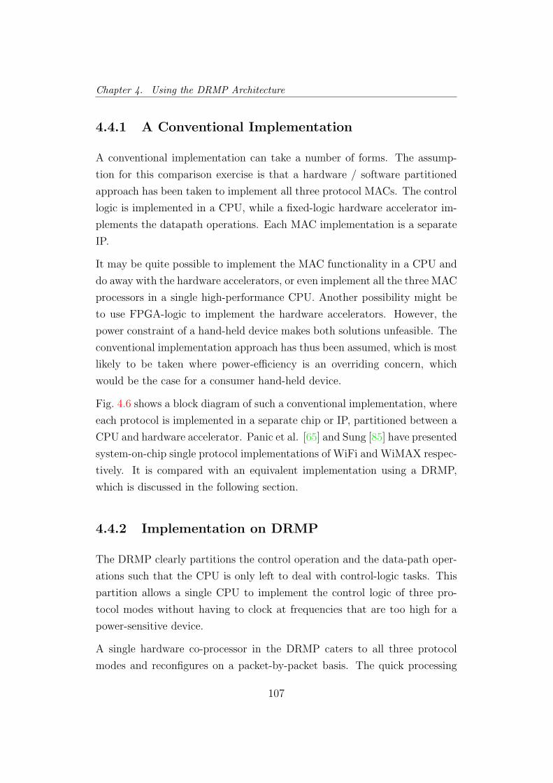
Chapter 4. Using the DRMP Architecture
4.4.1 A Conventional Implementation
A conventional implementation can take a number of forms. The assump-
tion for this comparison exercise is that a hardware / software partitioned
approach has been taken to implement all three protocol MACs. The control
logic is implemented in a CPU, while a fixed-logic hardware accelerator im-
plements the datapath operations. Each MAC implementation is a separate
IP.
It may be quite possible to implement the MAC functionality in a CPU and
do away with the hardware accelerators, or even implement all the three MAC
processors in a single high-performance CPU. Another possibility might be
to use FPGA-logic to implement the hardware accelerators. However, the
power constraint of a hand-held device makes both solutions unfeasible. The
conventional implementation approach has thus been assumed, which is most
likely to be taken where power-efficiency is an overriding concern, which
would be the case for a consumer hand-held device.
Fig. 4.6 shows a block diagram of such a conventional implementation, where
each protocol is implemented in a separate chip or IP, partitioned between a
CPU and hardware accelerator. Panic et al. [65] and Sung [85] have presented
system-on-chip single protocol implementations of WiFi and WiMAX respec-
tively. It is compared with an equivalent implementation using a DRMP,
which is discussed in the following section.
4.4.2 Implementation on DRMP
The DRMP clearly partitions the control operation and the data-path oper-
ations such that the CPU is only left to deal with control-logic tasks. This
partition allows a single CPU to implement the control logic of three pro-
tocol modes without having to clock at frequencies that are too high for a
power-sensitive device.
A single hardware co-processor in the DRMP caters to all three protocol
modes and reconfigures on a packet-by-packet basis. The quick processing
107

Chapter 4. Using the DRMP Architecture
DRMP
Dynamically Reconfigurable Hardware Accelerator
Application Processor
Driver A Driver B Driver C
MAC Processor A
CPU(Control Logic A)
Hardware Accelerator A
MAC Processor B
CPU(Control Logic B)
Hardware Accelerator B
MAC Processor C
CPU(Control Logic C)
Hardware Accelerator C
PHY A
(a) Conventional Implementation of a Multi-Standard Wireless Device
PHY B PHY C
If flexibility is desired for future-proofing, the entire MACs may be implemented in a high-performance CPU. Another option would be to use FPGA-logic to implement the hardware accelerator(s).
Application Processor
DRMP Driver
Accelerated Tasks B
Accelerated Tasks A
Accelerated Tasks C
CPU(Control Logic A, B and C)
PHY A PHY B PHY C
The CPU implements the control-logic in an interrupt-driven manner. The Hardware Co-Processor can reconfigure packet-to-packet to service packets of different protocol modes.
(b) Implementation of a Multi-Standard Wireless Device Using the DRMP
Figure 4.6: Implementation of three different MAC protocols in a multi-standard, power-sensitive wireless device (Conventional Implementation vs.Implementation Using DRMP)
108

Chapter 4. Using the DRMP Architecture
enabled by hardware acceleration of key tasks allows these tasks to be carried
out in a fraction of the packet duration. Hence, while functional units in
the hardware co-processor are together processing any one protocol mode
at a time (time-multiplex sharing), the hardware co-processor on the whole
handles three data streams of three protocol modes concurrently.
The control-logic is implemented in an interrupt-driven manner that allows
three protocol modes to use a single CPU to execute their control logic with-
out the overhead of a scheduling mechanism.
See Fig. 4.6 where an implementation with the DRMP is shown against a
conventional implementation.
4.4.2.1 Sequence of Functions
To illustrate the unique operations of the DRMP, and how it is different from
a conventional implementation, a sequence diagram is shown in fig. 4.7 for
two modes requesting service from the same RFU one after the other, as they
both attempt to transmit a packet. The complete operation is not shown in
the sequence diagram, but it can be seen how the various entities inside the
DRMP interact in a way that works for three protocol modes simultaneously
transmitting (only two shown for clarity).
109
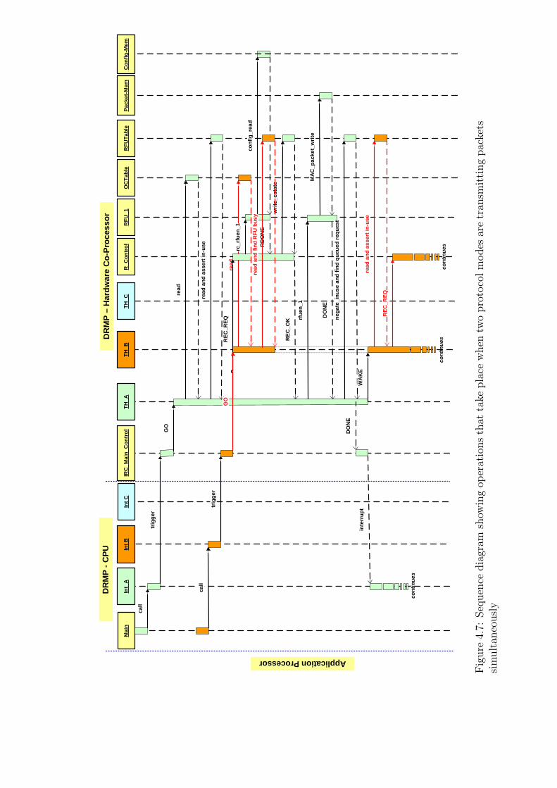
read
Int_
AIn
t BIn
t CIR
C_M
ain_
Con
trol
TH_A
TH_B
TH_C
R_C
ontr
olR
FU_1
Pack
et-M
em
trig
ger
RFU
Tabl
eO
CTa
ble
REC
_REQ
rc_r
fuen
_1
conf
ig_r
ead
read
GO
read
and
ass
ert i
n-us
e RD
ON
E
writ
e_cs
tate
REC
_OK rf
uen_
1
MA
C_p
acke
t_w
rite
DO
NE
nega
te_i
nuse
and
find
que
ued
requ
est
DO
NE
inte
rrup
t
Con
fig-M
emM
ain
call
DR
MP
-CPU
DR
MP
– H
ardw
are
Co-
Proc
esso
r
Application Processor
call
trig
ger
GO
read
and
find
RFU
bus
y
WA
KE
read
and
ass
ert i
n-us
e
REC
_REQ
cont
inue
sco
ntin
ues
cont
inue
s
Fig
ure
4.7:
Seq
uen
cedia
gram
show
ing
oper
atio
ns
that
take
pla
cew
hen
two
pro
toco
lm
odes
are
tran
smit
ting
pac
kets
sim
ult
aneo
usl
y

Chapter 4. Using the DRMP Architecture
4.4.2.2 RFUs for WiFi, WiMAX and UWB
As a result of investigation of MAC commonalities, precedent research, and
using the partitioning logic discussed in section 3.6.2.3, a pool of RFUs has
been implemented in the prototype DRMP model that caters to a WiFi MAC
implementation. The two other protocols are also investigated, WiMAX
(IEEE Std. 802.16) and UWB (IEEE Std. 802.15.3). Section 2.3.2 dis-
cusses all three protocols, their similarities and differences, and appendix B
elaborates.
The RFUs expected to be incorporated to make the DRMP function for the
three protocols, are discussed in Table. 4.1. The RFUs specific to WiFi have
been abstractly modeled in the prototype model, while the RFUs for the other
two protocols have been investigated only. Further investigation is needed
to determine the most suitable set that can service not only these three
protocols, but also other protocol MACs that may require implementation
on the device. The scope for innovation is quite extensive in the investigation
for optimal RFUs and their implementation, and is outside the scope of this
thesis. There is some interesting work available that may be investigated for
designing function-specific reconfigurable RFUs for DRMP. E.g. Pionteck et
al. [69] present a dynamically reconfigurable function-unit for error detection
and correction in mobile terminals. The same authors have presented a
reconfigurable encryption engine for mobile terminals [68].
Table 4.1: RFUs expected to be used for WiFi, WiMAX and UWB
RFU Protocol-
Relevance
Functionality and Remarks
Make-
Frame RFU
WiFi, WiMAX
and UWB
Creates a basic frame by copying data
from a source location to the packet-
memory, and appends a header to it. Its
operation is similar to a DMA controller.
111

Chapter 4. Using the DRMP Architecture
continued from previous page
RFU Protocol-
Relevance
Functionality and Remarks
Fragmen-
tation RFU
WiFi, WiMAX
and UWB
Reads a packet from the packet-memory
and stores it back in fragments, repeat-
ing the header for each fragment.
Defrag-
mentation
RFU
WiFi, WiMAX
and UWB
Reads fragments of a packet from the
packet-memory and stores it back as a
single fragment that can be read by the
upper layers.
Crypto-
RFU
WiFi, WiMAX
and UWB
Encrypts and decrypts the incoming and
outgoing data as required. This can
be expected to be a complex RFU that
caters to to various encryption algo-
rithms as required by the three protocols
(i.e. RC4, DES, 3DES, AES). The simi-
larity of different algorithms may be used
to incorporate units (inside this RFU or
as a separate RFU) that best exploit this
similarity. As an example, Logger et al.
[51] propose a reconfigurable encryption
unit that can implement three different
encryption algorithms; RC4, DES and
3DES, while Pionteck et al. [68] present
the design of a reconfigurable encryption
engine for the AES algorithm supporting
all key lengths.
112

continued from previous page
RFU Protocol-
Relevance
Functionality and Remarks
Redundancy
Check RFU
WiFi, WiMAX
and UWB
Reads, creates and verifies redundancy
data like CRC which is required by all
three protocol modes. RFUs for encryp-
tion, decryption, transmission and recep-
tion would use this RFU to carry out the
redundancy creation and verification op-
eration they require. Pionteck et al. pro-
pose a reconfigurable function-unit for
error detection and correction in mobile
terminals [69, 70].
Transmission
RFU
WiFi, WiMAX
and UWB
Reads packet fragments from the packet-
memory, calculates and appends the re-
dundancy check value (using the CRC-
RFU), and then transmits the data to
the transmission buffer. The transmis-
sion buffer in turn conveys the data to
the PHY layer, via a protocol compliant
wrapper.
Reception
RFU
WiFi, WiMAX
and UWB
Receives data from the reception buffer
(which is receiving data from the PHY
via a protocol compliant wrapper), cal-
culates and validates the redundancy
check value, and stores the data in the
packet-memory.
ACK Con-
trol RFU
WiFi and UWB MAC protocols some times require ACK
packets to be sent very quickly. This
dedicated RFU would generate and
transmit ACK packets quickly without
involving the CPU. Such an RFU would
eliminate the need for high-performance
CPU to create ACKs quickly. Such
an RFU is specially relevant in the
Immediate-ACK scheme of UWB.
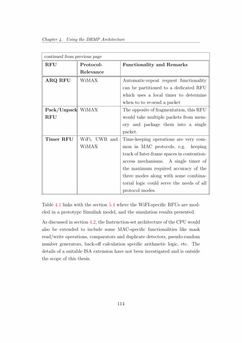
Chapter 4. Using the DRMP Architecture
continued from previous page
RFU Protocol-
Relevance
Functionality and Remarks
ARQ RFU WiMAX Automatic-repeat request functionality
can be partitioned to a dedicated RFU
which uses a local timer to determine
when to to re-send a packet
Pack/Unpack
RFU
WiMAX The opposite of fragmentation, this RFU
would take multiple packets from mem-
ory and package them into a single
packet.
Timer RFU WiFi, UWB and
WiMAX
Time-keeping operations are very com-
mon in MAC protocols, e.g. keeping
track of Inter-frame spaces in contention-
access mechanisms. A single timer of
the maximum required accuracy of the
three modes along with some combina-
torial logic could serve the needs of all
protocol modes.
Table 4.1 links with the section 5.4 where the WiFI-specific RFUs are mod-
eled in a prototype Simulink model, and the simulation results presented.
As discussed in section 4.2, the Instruction-set architecture of the CPU would
also be extended to include some MAC-specific functionalities like mask
read/write operations, comparators and duplicate detectors, pseudo-random
number generators, back-off calculation specific arithmetic logic, etc. The
details of a suitable ISA extension have not been investigated and is outside
the scope of this thesis.
114

Chapter 4. Using the DRMP Architecture
4.4.2.3 The Interrupt-Driven Software Implementation of MAC
Control
In section 4.1, it was discussed how the DRMP has a unique interrupt-driven
mechanism for implementing the protocol control of three MACs on a sin-
gle CPU. Fig. 4.8 and Fig. 4.9 show a WiFi-specific pseudo-code of such
an interrupt-handler showing the transmission of a packet. The complete
protocol implementation will have other control flows as well related to man-
agement operations. The other two protocol modes will have similar flows.
This chart links with section 5.4 where the WiFi-specific control flow is sim-
ulated as MATLAB code.
+ //======================================================== // Pseudo-Code of Interrupt Handler that Implements // Wifi MAC control (Transmission only) and uses DRMP API // to access Hardware Co-Processor (continues) //======================================================== //----------------------------- // State Encoding //----------------------------- // Every time the interrupt handler for Wifi is invoked // it is in one of the following states (Transmission only). // After executing some control logic, the state is // updated and contol passed to the RHCP or to the // Application Processor. sIDLE = 1;// Reset state, no state info sINIT = 2;// Protocol state-machine has been initialized, sIHEADER = 3;// State to write basic header sMKFRAME = 4;// State to make basic frame with payload sFRAGMENT = 5;// State for making Fragmentation request sENCRYPT = 6;// State for encryption sENCRYPT_POST = 7;// Post-encryption processing state sTRANSMIT = 8;// State for tranmission sTRANSMIT_POST= 9;// Post tranmission
Figure 4.8: Pseudo-code of interrupt handler that implements Wifi MACcontrol (transmission only) and uses the DRMP API. This figure shows thestate-encoding.
115

//============================================================= // Continued: Pseudo-Code of Interrupt Handler that Implements // Wifi MAC control (Transmission only) and uses DRMP API // to access Hardware Co-Processor //============================================================= //----------------------------------------- // Interrupt Handler for MAC Protocol A //----------------------------------------- switch(PSA.state) {
case sIDLE: Initialize_PSA_structure();
PSA.state = sINIT; case sINIT: // On receiving request from LLC Validate_request_parameters(); Update_PSA_structure();
PSA.state = sIHEADER; case sIHEADER: Write_basic_header_in_mem(); Initialize_pointers();
PSA.state = sMKFRAME;
case sMKFRAME: // Request RHCP to read LLC packet data // and store a basic frame in packet memory Request_RHCP_Service(CommandID, ProtocolMode, ARGS); PSA.state = sFRAGMENT;
case sFRAGMENT: Calculate_number_of_fragments(); Initialize_fragment_counter(); Calculate_first_fragment_size(); Initialize_encryption_pointer();
// Request RHCP to fragment packet Request_RHCP_Service(CommandID, ProtocolMode, ARGS); PSA.state = sENCRYPT; case sENCRYPT:
Update_fragment_counter(); // Request RHCP to encrypt packet
Request_RHCP_Service(CommandID, ProtocolMode, ARGS); PSA.state = sENCRYPT_POST; case sENCRYPT_POST: Update_header_of_fragment(); if (more fragments left in this packet) Update_next_fragment_size();
PSA.state = sENCRYPT else Reset_fragment_counter() Calculate_first_fragment_size();
PSA.state = sTRANSMIT
case sTRANSMIT: Update_fragment_counter(); // Request RHCP to calculate CRC and trasnmit to PHY
Request_RHCP_Service(CommandID, ProtocolMode, ARGS); PSA.state = sTRANSMIT_POST; case sTRANSMIT_POST:
if (more fragments left in this packet) Update_next_fragment_size();
PSA.state = sTRANSMIT; else Interrupt_Host_Indicate_Transmission_Complete()
PSA.state = sIDLE; }
Figure 4.9: Pseudo-code of interrupt handler that implements Wifi MAC con-trol (transmission only) and uses the DRMP API. This figure shows protocolstate-machine.

Chapter 5
Modeling and Simulation
A prototype model of the DRMP SoC has been designed in Simulink. In this
model, three packets, of three different protocol modes1have been successfully
transmitted and received concurrently. The model’s abstraction is discussed
in this chapter, along with the tools used, and then the results of simulation
runs are presented, their implications discussed.
Although a route to implementation in silicon has been considered, it was
not the main purpose of the modeling effort. The model was designed to
present a proof-of-concept of the architecture, to show that the unique de-
sign of the DRMP is capable of packet-by-packet reconfiguration to process
three concurrent protocol data streams, while the overheads and the clocking
frequency are kept low enough to make it feasible for hand-held devices.
5.1 Development Tools
The choice of development tools was an important and interesting decision
for this project. From the onset it became clear that the development envi-
ronment will have to cope with some unique requirements of this project:
1For the prototype, all three protocol ‘modes’ are actually implementing simplified Wififunctionality, but I assume they are different protocols and reconfigure the RFUs wheneverthere is a protocol mode switch.
117

Chapter 5. Modeling and Simulation
1. The project had a wide scope — a complete SoC for MAC is a complex
and large IP, and implementing it in Register transfer level (RTL) would
have been impractical in the life-time of an Engineering Doctorate.
2. The DRMP is a completely new and innovative architecture that has
been designed from scratch. Trials and corrections were expected dur-
ing the course of its development. The development tool should have
allowed that in a convenient way.
3. In some ways the architecture is a traditional hardware / software par-
titioned SoC. It was expected that for many parts of the SoC, there
was a very good option already available in the form of some precedent
research or a commercial IP. As such, all parts of the SoC design were
not ‘innovative’. It was decided therefore that the prototype model
would be kept at high-abstraction in general and only those parts of
the architecture would be detailed at a lower abstraction that added
value to the project and were innovative. This consideration implied a
development environment that supported a co-simulation environment
for different abstractions.
In view of the above considerations, SystemC was initially chosen to de-
velop the model, and its Transaction-Level Modeling library was considered
very useful. However, the Matlab and Simulink environment was eventually
considered more suitable for these considerations. The Stateflow toolbox
provided by Simulink proved very useful in modeling the control flow in the
DRMP. Toolboxes like Link for ModelSim, Stateflow Coder and Simulink
HDL Coder provide a convenient route to full implementation as well [55].
Another benefit of using a graphical tool like Simulink was that it made it
very easy to visualize a block-level view of the architecture. The visualization
assisted in the design of and improvements in the architecture, and also made
it easier to share and discuss amongst the people the involved in the research
effort. The control-flow visualization provided by Stateflow assisted in a
similar manner.
118

Chapter 5. Modeling and Simulation
5.2 Abstraction Level
The functionality is modeled at various levels of detail. The timing is cycle-
approximate. The bus-interface is approximate but more detailed than a
transaction-level model.
The model approximates the actual timing quite closely. E.g., when trans-
ferring a block of data, the required number of clocks are spent rather then
doing a block transfer on a single clock tick. The interface amongst the var-
ious blocks, though not pin-accurate, is also defined in considerable detail.
The point to note is that although the modeling is done on a tool capable of
various levels of abstraction, the route taken reveals detailed information in
two key areas: timing results and interconnect requirements2. Both of them
are the more critical indicators of the architecture’s success or otherwise. On
the flip side, one can make but vague approximations about the area and
power of the DRMP from this model of the architecture. However, a first-
order approximation is still possible, enough to decide if the area and power
usage is low enough for hand-held devices (See section 6.1).
Functional abstraction is not uniform across the model. The tasks parti-
tioned to software, primarily the high-level protocol state-machine, are mod-
eled with very little detail. Same goes for some operations in the hardware.
E.g. the encryption RFU is a dummy functionality-wise, but it spends the
required number of clock ticks for each byte (3 clock ticks / byte according
to [46]). But components like the Interface and Reconfiguration Controller
are modeled in much more detail, and little design effort will be needed to
derive the RTL design.
2The model is simulated with a clock, and for those blocks are modeled at high ab-straction or as stubs, clock cycles are wasted to ensure an accurate timing estimate. Thecommunication between blocks is also simulated with a clock, on interconnects of definedwidths.
119

Chapter 5. Modeling and Simulation
5.3 The Simulink Model
The Simulink Model of the DRMP models a transmitting and a receiving
wireless device. A GUI can be used to set parameters like the frequency of
the protocols, the size of packet data to be transmitted, the clock frequency of
the hardware etc. A scripts initializes parameters at beginning of simulation.
Once the simulation is complete, another script collects the results, indicates
if the data was successfully received, and generates various plots that show
the behavior of the model for that simulation run—some of these plots appear
in the next section. Some snapshots from the model appear in Appendix A.
5.4 Simulation Results
On a prototype DRMP model in Simulink, successful simulations of concur-
rent transmission and reception of 3 packets, fragmented as required, were
carried out. The packets were assumed to be of 3 different protocols.
When the DRMP architecture was being designed, the decision to incorpo-
rate concurrent processing of three modes was based on the estimates that
considerable time slack will be available in the DRMP. The time taken to
process a packet was expected be considerably less than the packet duration.
This observation was used as a basis to propose that a packet-by-packet re-
configuration would be possible, and also that there would be room for power
efficiency improvement by trading off this time slack. The simulation results
confirmed the assumption as the following sections indicate.
5.4.1 Simulation Run with One Protocol Mode
Simulations were run involving transmission and reception of a Wifi packet
on the prototype model, and the results showed that the processing of packet
on the DRMP architecture indeed took a fraction of the actual duration of
the packet. Fig. 5.1 shows the output taken directly from the simulation
120

Chapter 5. Modeling and Simulation
showing the active and idle times of various blocks in the DRMP during
the transmission of a packet. It clearly indicates that various RFUs as well
as the controllers are busy for only a fraction of the duration of the packet
transmission. The RFUs do their job very quickly and store the formatted
packet in the buffer, ready to be sent, in a fraction of even the first fragments
transmission duration. The buffer then sends out these fragments (in bytes)
at the frequency expected by the protocol. The active time of the buffer in
Fig. 5.1 and subsequent figures thus represents the actual protocol packet
duration.
Fig. 5.2 shows a similar situation for the packet reception, with the RFUs
busy for a fraction of the duration of packet reception. The name of the
RFUs in these figures correspond to the RFUs discussed earlier in Table 4.1.
The size of the packet is 200 bytes, and an arbitrary fragmentation threshold
of 80 bytes results in three fragments being sent, which can be seen in the
timing diagram. The architecture is assumed to run at a frequency of 200
MHz—a realistic frequency for hand held devices. The timing axis is appro-
priately scaled to represent time in microseconds. The exchange of data with
the PHY is modeled at 20 Mbps.
The simulation results of simulating 1 mode on the prototype model were
very promising. They clearly indicated that the DRMP architecture would
be capable of handling parallel streams of data, since its various entities
were busy for only a fraction of actual packet durations. They could be
reconfigured and used for other protocols in their idle time. The idle time
also opened doors for power-efficiency improvement.
5.4.2 Simulation Run with Three Concurrent Protocol
Modes
After simulating a single protocol mode on the architecture, I then proceeded
to test the packet-by-packet reconfiguration and concurrent processing of
three protocol modes on the architecture.
121

Chapter 5. Modeling and Simulation
0 20 40 60 80 100 120 140IDLE
BUSY
MAC Microprocessor
0 20 40 60 80 100 120 140IDLE
BUSY
Task Handler for MAC Operations (Mode 1)
0 20 40 60 80 100 120 140IDLE
BUSY
Reconfiguration Controller
0 20 40 60 80 100 120 140IDLE
BUSY
RFU for Making Basic MAC Frame
0 20 40 60 80 100 120 140IDLE
BUSY
RFU for Fragmentation
0 20 40 60 80 100 120 140IDLE
BUSY
RFU for Encryption
0 20 40 60 80 100 120 140IDLE
BUSY
RFU for CRC
0 20 40 60 80 100 120 140IDLE
BUSY
RFU for Tx to PHY
0 20 40 60 80 100 120 140IDLE
BUSY
Tx Buffer Interface with PHY (Actual Duration of Tranmission)
SIMULATION TIME IN MICROSECONDS
Figure 5.1: Activity Timing Diagram of Blocks in the DRMP Architecture(Packet Transmission of 1 Mode)
Application processor of the transmitting device sends three packets, each
packet of a separate protocol data stream. The DRMP processes these pack-
ets one by one, reconfiguring RFUs as it switches from one mode to another,
and then stores packets in their respective transmit buffers. The receiving
device receives these packets concurrently in its buffers, the MAC processing
is done in the DRMP sequentially, the RFUs reconfigured and shared among
the three modes.
The size of the packet in each mode is 200 bytes, broken into 3 fragments.
The architecture is assumed to run at a frequency of 200 MHz. The exchange
of data with the PHY is modeled at 20 Mbps for all three modes.
Fig. 5.3 shows the output taken directly from the simulation showing the
122

Chapter 5. Modeling and Simulation
50 100 150 200IDLE
BUSY
MAC Microprocessor
50 100 150 200IDLE
BUSY
Task Handler for MAC Operations (Mode 1)
50 100 150 200IDLE
BUSY
Reconfiguration Controller
50 100 150 200IDLE
BUSY
RFU for Defragmentation
50 100 150 200IDLE
BUSY
RFU for Decryption
50 100 150 200IDLE
BUSY
RFU for CRC
50 100 150 200IDLE
BUSY
RFU for Rx from PHY
50 100 150 200IDLE
BUSY
Rx Buffer Interface with PHY (Actual Duration of Reception)
SIMULATION TIME IN MICROSECONDS
Figure 5.2: Activity Timing Diagram of Blocks in the DRMP Architecture(Packet Reception of 1 Mode)
active and idle times of various blocks in the DRMP for the first 30 mi-
croseconds of the transmission of the three packets. Note that that while the
task-handlers and the buffers—unique to each protocol mode—run concur-
rently, the RFUs are time-multiplexed among the three protocol modes. Yet,
the packets are processed and ready to be sent in a fraction of the packet
durations. Fig. 5.4 shows a similar situation for the packet reception (with
complete packet duration shown).
Tables 5.1 and 5.2 show the actual and proportional durations that the blocks
are busy during transmission and reception. These results have been com-
pared with results from a simulation with one protocol mode. It can be seen
that e.g. RFU for encryption (which has the highest clocks/byte ratio) is ac-
tive for 12.1% of the duration of packet transmission, when all three modes
123

Chapter 5. Modeling and Simulation
The Various Blocks of the DRMPtake less than 30 microsecondsto process the 3 Packets, eachwith 3 fragments each, and eachbelonging to a different protocolmode. For the rest of the packet’sprotocol duration, they are Idle.The Activity of the various blocksin the DRMP during the first 30microseconds is shown in detailbelow.
30 MICROSECONDS
PACKET DURATION (AT 20 Mbps) =
120 MICROSECONDS
0 5 10 15 20 25 30IDLE
BUSY ABUSY BBUSY C
MAC MICROPROCESSOR
0 5 10 15 20 25 30IDLE
BUSY ABUSY BBUSY C
TASK HANDLER FOR MAC OPERATIONS
0 5 10 15 20 25 30IDLE
BUSY
RECONFIGURATION CONTROLLER
0 5 10 15 20 25 30IDLE
BUSY
RFU FOR MAKING BASIC MAC FRAME
0 5 10 15 20 25 30IDLE
BUSY
RFU FOR FRAGMENTATION
0 5 10 15 20 25 30IDLE
BUSY
RFU FOR ENCRYPTION
0 5 10 15 20 25 30IDLE
BUSY
RFU FOR CRC
0 5 10 15 20 25 30IDLE
BUSY
RFU FOR Tx TO PHY
0 5 10 15 20 25 30IDLE
BUSY ABUSY BBUSY C
Tx BUFFER INTERFACE WITH PHY (ACTUAL DURATION OF TRANSMISSION
Simulation Time in Microseconds
0 20 40 60 80 100 120 140 160IDLE
BUSY ABUSY BBUSY C
MAC MICROPROCESSOR
0 20 40 60 80 100 120 140 160IDLE
BUSY ABUSY BBUSY C
TASK HANDLER FOR MAC OPERATIONS
0 20 40 60 80 100 120 140 160IDLE
BUSY
RECONFIGURATION CONTROLLER
0 20 40 60 80 100 120 140 160IDLE
BUSY
RFU FOR MAKING BASIC MAC FRAME
0 20 40 60 80 100 120 140 160IDLE
BUSY
RFU FOR FRAGMENTATION
0 20 40 60 80 100 120 140 160IDLE
BUSY
RFU FOR ENCRYPTION
0 20 40 60 80 100 120 140 160IDLE
BUSY
RFU FOR CRC
0 20 40 60 80 100 120 140 160IDLE
BUSY
RFU FOR Tx TO PHY
0 20 40 60 80 100 120 140 160IDLE
BUSY ABUSY BBUSY C
Tx BUFFER INTERFACE WITH PHY (ACTUAL DURATION OF TRANSMISSION
Simulation Time in Microseconds
Figure 5.3: Activity Timing Diagram of Blocks in the DRMP Architecture(Packet Transmission of 3 Modes)
124
Chapter 5. Modeling and Simulation
60 80 100 120 140 160 180 200 220IDLE
BUSYABUSYB
BUSYC
MAC Microprocessor
60 80 100 120 140 160 180 200 220IDLE
BUSYIDLE
BUSY
Task Handler for MAC Operations
60 80 100 120 140 160 180 200 220IDLE
BUSY
Reconfiguration Controller
60 80 100 120 140 160 180 200 220IDLE
BUSY
RFU for Defragmentation
60 80 100 120 140 160 180 200 220IDLE
BUSY
RFU for Decryption
60 80 100 120 140 160 180 200 220IDLE
BUSY
RFU for CRC
60 80 100 120 140 160 180 200 220IDLE
BUSY
RFU for Rx from PHY
60 80 100 120 140 160 180 200 220IDLE
BUSYABUSYB
BUSYC
Rx Buffer Interface with PHY (Actual Duration of Reception)
Simulation Time in Microseconds
Figure 5.4: Activity Timing Diagram of Blocks in the DRMP Architecture(Packet Reception of 3 Modes)
are concurrently transmitting. Note that the Task-Handler, showing a 13%
busy time, is not a shared resource. Each of the three protocol modes has
one of its own.
5.4.3 Results for the IRC
A more detailed look into various states that the Interface and Reconfigura-
tion Controller takes while in operation gives valuable information about the
usage of shared resources.
Fig. 5.5 shows the various active states inside the Task-Handler for MAC
(TH M) of the three modes when a packet is sent by the three modes concur-
rently. All three modes currently simulate the same protocol i.e. WiFi, and
125

Chapter 5. Modeling and Simulation
Table 5.1: Busy Time of Various Entities in DRMP During Transmissionµs % of Packet Duration
Entity 1 Mode 3 Modes 1 Mode 3 ModesTask HandlerMAC, Mode A
9.1 16.9 7.0 13.1
Reconf’n Con-trol
0.1 1.0 0.1 0.8
RFU-MakeFrame
0.8 2.5 0.6 1.9
RFU-Frag’t 1.3 3.9 1.0 3.0RFU-Encrypt 4.0 12.1 3.1 9.4RFU-CRC 5.4 16.3 4.2 12.6RFU-Tx 2.0 6.3 1.6 4.9Tx-Buffer,ModeA
128.9 128.9 100.0 100.0
hence all three modes would need the RFUs in the same configuration state.
However, to get realistic results, the RFUs are reconfigured every time there
is a mode switch. Fig. 5.6 is a similar timing diagram for the Task-handler for
Reconfiguration (TH R) of the three modes. The value on the x-axis is time
in microseconds. The name of the various states correspond to the states in
the statechart in Fig. 3.6 and Fig. 3.5 in section 3.6.1.2. Some states indicate
the controller using a resource, while some indicate the controller waiting
for a resource to become free. This timing diagram indicates how the three
task-handlers work concurrently to provide a mechanism where three proto-
col modes access shared resources, with RFU’s dynamically reconfigured as
required. Note that all the activity of the three task-handlers is completed in
less than 10µs. Looking at Fig. 5.3 it can be clearly seen that the complete
active duration of a task-handler for MAC, during which cycles through its
state-machine and does all the tasks required to transmit a packet, is a small
fraction (13%) of the packet duration.
In Fig. 5.7, the first few microseconds of Fig. 5.5 are magnified, to show
more clearly the relationship between the three concurrent task-handlers,
and how they access shared resources. E.g. between 1.5µs and 3µs, one can
see that Mode B acquires the packet-bus (goes into USE PBUS state), and
126

Chapter 5. Modeling and Simulation
Table 5.2: Busy Time of Various Entities in DRMP During Receptionµs % of Packet Duration
Entity 1 Mode 3 Modes 1 Mode 3 ModesTask HandlerMAC, Mode A
7.8 8.6 6.0 6.7
Reconf’n Con-trol
0.1 0.6 0.1 0.5
RFU-Defrag’t 1.1 3.0 0.8 2.3RFU-Decrypt 4.2 11.5 3.2 8.9RFU-CRC 5.3 15.1 4.1 11.7RFU-Rx 1.6 5.0 1.2 3.9Rx-Buffer,ModeA
129.2 129.2 100.0 100.0
0 5 10 15 20 25 30IDLE
ACTIVE
WAIT4OCT
USE_OCT
WAIT4RFU1
USE_RFU1
WAIT4PBUS
USE_PBUS
WAIT4RFUdone
WAIT4RFUT2
USERFUT2
SLEEP1
SLEEP2
Simulation Time in Microseconds
Mode AMode BMode C
Figure 5.5: Timing Diagram Showing State Occupation in a Task-Handlerfor MAC During Packet Transmission
then proceeds to the WAIT4RFUdone state where it has triggered an RFU and
is waiting for response. The packet-bus is still with Mode B and one can
see Mode A stuck in the WAIT4PBUS state, waiting for the packet-bus to
127
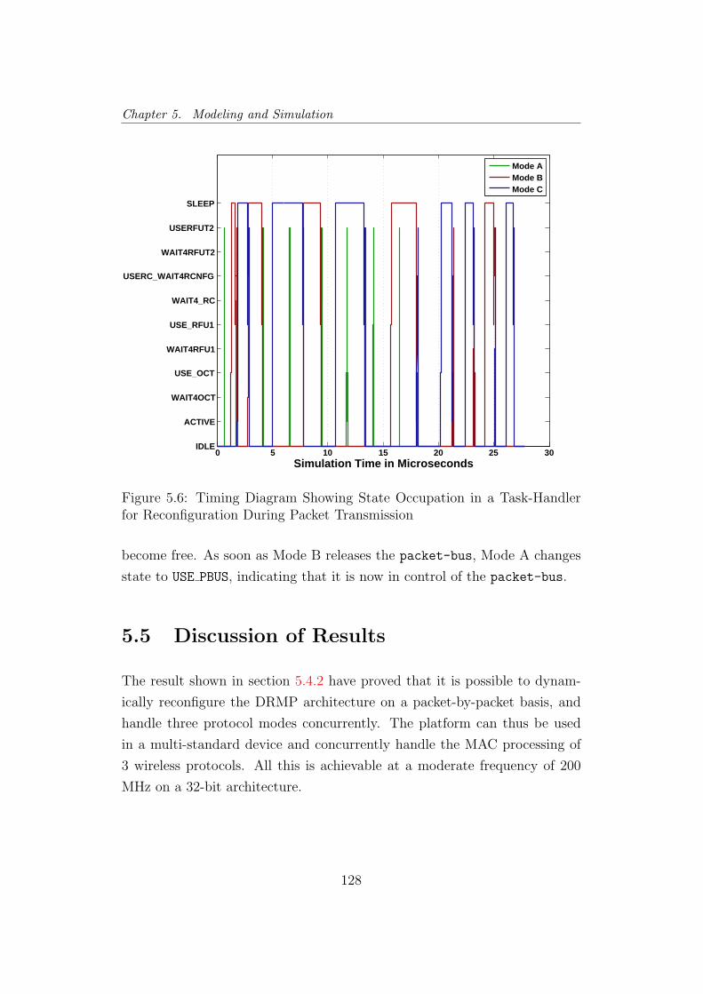
Chapter 5. Modeling and Simulation
0 5 10 15 20 25 30IDLE
ACTIVE
WAIT4OCT
USE_OCT
WAIT4RFU1
USE_RFU1
WAIT4_RC
USERC_WAIT4RCNFG
WAIT4RFUT2
USERFUT2
SLEEP
Simulation Time in Microseconds
Mode AMode BMode C
Figure 5.6: Timing Diagram Showing State Occupation in a Task-Handlerfor Reconfiguration During Packet Transmission
become free. As soon as Mode B releases the packet-bus, Mode A changes
state to USE PBUS, indicating that it is now in control of the packet-bus.
5.5 Discussion of Results
The result shown in section 5.4.2 have proved that it is possible to dynam-
ically reconfigure the DRMP architecture on a packet-by-packet basis, and
handle three protocol modes concurrently. The platform can thus be used
in a multi-standard device and concurrently handle the MAC processing of
3 wireless protocols. All this is achievable at a moderate frequency of 200
MHz on a 32-bit architecture.
128

Chapter 5. Modeling and Simulation
0 0.5 1 1.5 2 2.5 3 3.5 4 4.5 5IDLE
ACTIVE
WAIT4OCT
USE_OCT
WAIT4RFU1
USE_RFU1
WAIT4PBUS
USE_PBUS
WAIT4RFUdone
WAIT4RFUT2
USERFUT2
SLEEP1
SLEEP2
Simulation Time in Microseconds
Mode AMode BMode C
Figure 5.7: Timing Diagram Showing State Occupation in a TH M DuringPacket Transmission, with the first few Microseconds Magnified
5.5.1 Time Slack and Reducing Power Consumption
Its worth pointing out that large parts of the architecture are idle even when
three modes run concurrently—a typical RFU is active for around 10% of
packet duration. In fact, when just one mode is active, which one can expect
to be the case for most of the time the device is being used, the RFUs are
typically busy for less than 5% to process a packet. Considerable power can
be saved by exploiting this time lag: E.g. parts of the DRMP can be switched
off when idle; or one could e.g. dynamically scale the operating frequency so
that the DRMP’s throughput is just fast enough to meet real-time protocol
constraints, and no more.
The simulation results from the prototype model are very promising. They
clearly indicate that the DRMP architecture is be capable of handling parallel
streams of data, since its various entities are busy for only a fraction of
129
Chapter 5. Modeling and Simulation
actual packet durations. These units can be reconfigured and used for other
protocols in their idle time. The idle time also implies that one can use high-
latency reconfiguration mechanisms that yield better power-efficiency than
other high-speed reconfiguration mechanisms, as discussed in section 6.2.
Moreover, hardware co-processor can be clocked at slower frequencies than
the current 200 MHz assumed, which also means better power-efficiency.
Compared to general-purpose reconfigurable architectures like FPGAs, the
DRMP needs less interconnect resources. Moreover, heterogeneous function-
specific reconfigurable units will need less configuration data than general-
purpose units like LUT based logic blocks. All these features would add up
to give power-efficient flexibility in the DRMP.
There is another outcome of these results. The DRMP is a modular archi-
tecture, with only certain parts of the architecture working at one time and
the others idle. Idle, in context, means an entity is not active and also is in
its reset state. Effectively, it can be switched off when it is idle, without in-
curring the overheads associated with saving and restoring state information.
Considering that a typical RFU is active for around 5% of the time with a sin-
gle active mode, one can save considerable power this way. Power-efficiency
improvement is discussed further in section 6.2.
These results show that the DRMP — a dynamically reconfigurable archi-
tecture — implements the MAC layer of WiFi with minimal timing overhead
introduced by the architecture. In fact, the modular design makes it possible
to take large parts of the hardware off-line for most of the device’s up-time.
These features are very different from alternative flexible solutions like an
FPGA or a microprocessor. I am confident of achieving the target of im-
plementing three parallel streams in this prototype, reconfiguring packet to
packet, yet at moderate power consumption suitable for hand-held devices.
5.5.2 Frequency of Operation
The results shown in the section 5.4 and discussed here were for a clock
frequency of 200 MHz. The frequency chosen was ad-hoc, a value that can
130
Chapter 5. Modeling and Simulation
be considered suitable for power-sensitive hand-held devices. It was seen
that at this frequency, and with three protocols simultaneously transmitting,
there was considerable time-slack available, as was clearly shown in Fig. 5.3.
Keeping all other simulation parameters the same, an interesting question
is of how low a frequency can be used and yet process the three packets
in time. In context of concurrent transmission of three packets of different
protocols, the criteria of the DRMP meeting throughput requirements is that
it should complete the MAC processing of all three protocols and store them
in the transmit buffers, ready to be sent, within one packet duration from
the moment the request for transmission is made (in the simulation setup
the three protocol modes make transmission request almost simultaneously).
Looking again at the case where the architecture was running at 200 MHz,
and the duration of packets was 120 microseconds, it was seen that the three
packets were processed in a little less than 30 microseconds. Fig. 5.8 shows
this situation again.
It can be deduced that were one to run the architecture at one-fourth the
original speed, it should still be able to meet the real-time requirements. Such
a simulation was carried out, reducing the architecture frequency to 50 MHz.
Fig. 5.9 shows the result of the transmit side of this simulation. It can be
seen that the MAC processing for all the three protocols is completed inside
120 microseconds, which is the protocol duration of the three fragments of a
packet.
5.5.3 Single Protocol vs. Three Concurrent Protocols’
Operation
Fig. 5.10 shows this comparison of resource usage between one mode opera-
tion and three mode operation. The busy time of various entities is shows as
a percentage of the total packet duration. Since the three modes were mod-
eled at the same data rate of 20 Mbps, and were sending packets of same
sizes, the busy time of the functional units increases by approximately three
131
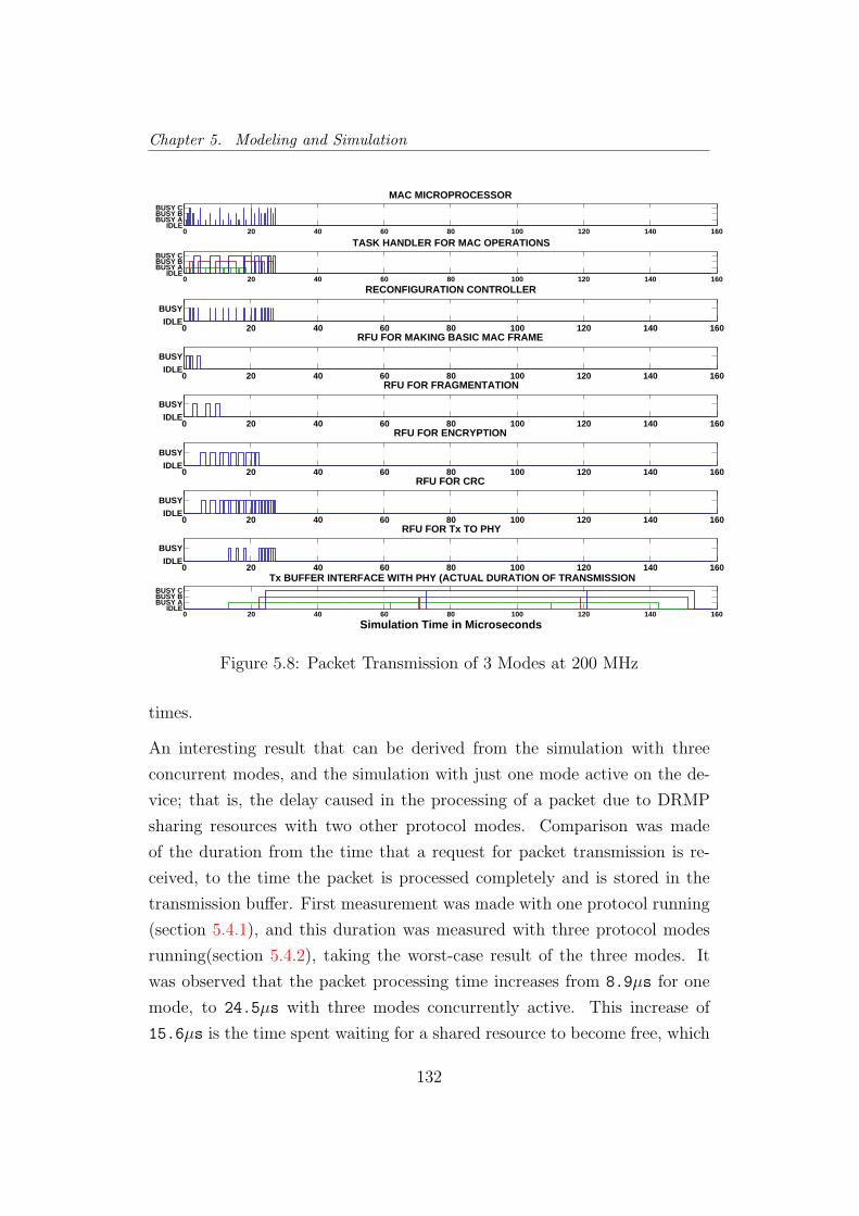
Chapter 5. Modeling and Simulation
0 20 40 60 80 100 120 140 160IDLE
BUSY ABUSY BBUSY C
MAC MICROPROCESSOR
0 20 40 60 80 100 120 140 160IDLE
BUSY ABUSY BBUSY C
TASK HANDLER FOR MAC OPERATIONS
0 20 40 60 80 100 120 140 160IDLE
BUSY
RECONFIGURATION CONTROLLER
0 20 40 60 80 100 120 140 160IDLE
BUSY
RFU FOR MAKING BASIC MAC FRAME
0 20 40 60 80 100 120 140 160IDLE
BUSY
RFU FOR FRAGMENTATION
0 20 40 60 80 100 120 140 160IDLE
BUSY
RFU FOR ENCRYPTION
0 20 40 60 80 100 120 140 160IDLE
BUSY
RFU FOR CRC
0 20 40 60 80 100 120 140 160IDLE
BUSY
RFU FOR Tx TO PHY
0 20 40 60 80 100 120 140 160IDLE
BUSY ABUSY BBUSY C
Tx BUFFER INTERFACE WITH PHY (ACTUAL DURATION OF TRANSMISSION
Simulation Time in Microseconds
Figure 5.8: Packet Transmission of 3 Modes at 200 MHz
times.
An interesting result that can be derived from the simulation with three
concurrent modes, and the simulation with just one mode active on the de-
vice; that is, the delay caused in the processing of a packet due to DRMP
sharing resources with two other protocol modes. Comparison was made
of the duration from the time that a request for packet transmission is re-
ceived, to the time the packet is processed completely and is stored in the
transmission buffer. First measurement was made with one protocol running
(section 5.4.1), and this duration was measured with three protocol modes
running(section 5.4.2), taking the worst-case result of the three modes. It
was observed that the packet processing time increases from 8.9µs for one
mode, to 24.5µs with three modes concurrently active. This increase of
15.6µs is the time spent waiting for a shared resource to become free, which
132

Chapter 5. Modeling and Simulation
0 50 100 150 200 250IDLE
BUSY ABUSY BBUSY C
MAC MICROPROCESSOR
0 50 100 150 200 250IDLE
BUSY ABUSY BBUSY C
TASK HANDLER FOR MAC OPERATIONS
0 50 100 150 200 250IDLE
BUSY
RECONFIGURATION CONTROLLER
0 50 100 150 200 250IDLE
BUSY
RFU FOR MAKING BASIC MAC FRAME
0 50 100 150 200 250IDLE
BUSY
RFU FOR FRAGMENTATION
0 50 100 150 200 250IDLE
BUSY
RFU FOR ENCRYPTION
0 50 100 150 200 250IDLE
BUSY
RFU FOR CRC
0 50 100 150 200 250IDLE
BUSY
RFU FOR Tx TO PHY
0 50 100 150 200 250IDLE
BUSY ABUSY BBUSY C
Tx BUFFER INTERFACE WITH PHY (ACTUAL DURATION OF TRANSMISSION
Simulation Time in Microseconds
Figure 5.9: Packet Transmission of 3 Modes at 50 MHz
is still a fraction of the packet duration. This result is shown is a pie-chart
in Fig. 5.11. It shows time a mode spends active on the DRMP, waiting for
a shared resource, or idle, as a proportion of the total packet duration of
128.9µs. The operating frequency of the architecture is 200 MHz. It can be
concluded that the processing lag experienced by one protocol mode due to
resource sharing of the DRMP amongst two other modes is not significant,
and there is still a significant time slack, as can be seen from Fig. 5.11.
5.5.4 The Interface and Reconfiguration Controller
Looking more closely inside the IRC, another interesting result can be derived
(Fig. 5.5); what is the critical shared resource that determines the over-all
time that the IRC takes to complete its task? The TH M and not the TH R is
133

Chapter 5. Modeling and Simulation
7.0
13.1
0.10.8 0.6
1.9
1.0
3.03.1
9.4
4.2
12.6
1.6
4.9
0.0
2.0
4.0
6.0
8.0
10.0
12.0
14.0
Bus
y Ti
me
(% o
f Pac
ket D
urat
ion)
TaskHandler R-Cont'l RFU-MakeFrame
RFU-Frag'n RFU-Encrypt RFU-CRC RFU-Tx
1 mode3 concurrent modes
Figure 5.10: Comparison of resource usage between one mode transmissionand three mode concurrent transmission. Shown as percentage of packetduration.
considered because the TH M is the more critical controller that has to ensure
that the MAC related tasks are carried out in the required time. This issue
is important because it determines the bottleneck that will put a limit on the
maximum throughput of the device. It can be seen that the task-handlers
are waiting most often for the Packet-bus to become free.
Fig. 5.12 presents this result quantitatively and it can be seen that the three
TH M are in the WAIT4PBUS state, waiting for the Packet bus to become
free, for around 20–30% of their active times, which is more than any other
idle waiting state. Note that the WAIT4RFUDONE is not an idle waiting state
caused by contention on a shared resource—it is the Task-handler waiting for
an RFU to complete a task it has been assigned. In this sense, this is actually
an active state for that protocol mode. Hence this state is not counted when
trying to determine the critical shared resource.
134

Chapter 5. Modeling and Simulation
Waiting for a shared resource,
15.6us, 12%
Active on the DRMP, 8.9us, 7%
Idle / Slack time, 104.4us, 81%
Figure 5.11: Time a mode spends: active on the DRMP, waiting for a sharedresource, or idle. Shown as a proportion of the total packet duration of128.9µs, when three modes are concurrently transmitting. Operating fre-quency is 200 MHz.
The behavior of the IRC during simulation runs indicates that if, because
of higher bandwidth protocols or introduction of more than three protocol
modes, the DRMP fails to process packets in the required time, the inter-
connect will be the bottleneck that will need a redesign. It is important to
note that the percentages shown are percentage of the active time of a TH M.
From Table. 5.1, one can see that the complete active time of a TH M is itself
a mere 13% of the actual Wifi packet duration, so such a scenario of faliure
to meet protocol timing requirements is unlikely.
The most sought-after shared resource in the DRMP architecture is the bus
that connects the RFUs to each other and the memory. At some point, due
to increase in data rates or perhaps introduction of more protocol modes,
this resource will become saturated. It may then be required to introduce a
secondary interconnect to allow true concurrent use of RHCP by the different
modes, or one could simply clock the architecture faster.
135

Chapter 5. Modeling and Simulation
0.0
5.0
10.0
15.0
20.0
25.0
30.0
35.0
40.0
ACTIVE
WAIT4OCT
USE_OCT
WAIT4RFU1
USE_RFU1
WAIT4PBUS
USE_PBUS
WAIT4RFUdone
WAIT4RFUT2
USERFUT2
SLEEP1
SLEEP2
State of TH_M
Act
ive
Dur
atio
n (P
erce
ntag
e of
Tot
al A
ctiv
e D
urat
ion)
Mode A Mode B Mode C
Figure 5.12: Active Time of Various States in the Task-handler for MAC asa Percentage of its Total Active Time
5.5.5 Performance Assumptions (Software and Recon-
figuration)
The DRMP prototype models the transmission and reception of packets,
loosely following the WiFi protocol. The software in the DRMP simply
keeps track of the state of the system and does not perform computationally
intensive tasks. It is completely interrupt-driven and only generates control
signals, resulting in a very simple, lightweight API, as discussed in some
detail in section 4.1. The protocol control tasks the software is left to perform
between calls to the the RHCP can be implemented in a CPU running at
moderate frequencies. A frequency of 200 MHz has been assumed, same as
the assumed operating frequency of the hardware co-processor, which is a
suitable one for hand-held devices.
The DRMP is a hardware / software partitioned architecture and the func-
tionality of both the hardware and software has been modeled. However, the
136
Chapter 5. Modeling and Simulation
software functionality is modeled at a more abstract level than the hardware.
Panic et al. [65] state that a pure software implementation of the WiFi MAC
layer will need to run on a CPU clocked at nearly 1 GHz. It then goes on to
propose a software / hardware partitioned SoC solution with an operating fre-
quency of 80 MHz. The tasks partitioned by Panic et al. [65] to hardware are
very similar to the partitioning done in the DRMP. However, their hardware
is not reconfigurable. More importantly, their hardware/software partition-
ing offloads less functionality to the Hardware than the DRMP. Considering
the time-slack available even when three protocol are transmitting concur-
rently, one can be confident that the 80MHz quoted in [65] will constitute
an upper limit to the required clock frequency of the microprocessor. Also
refer to Fig. 4.9 in section 4.4 where a more detailed view of the tasks that
the software performs between calls to the hardware, and the relatively few
software instructions/CPU clock cycles needed to implemented these tasks
can be inferred.
Currently most of the RFUs have been modeled as context-switching RFUs,
while when three different protocols are actually deployed, some RFUs may
be reading configuration data from a memory on a mode switch. However,
because the RFUs are function-specific, it is safe to assume that the config-
uration data will be very little compared to more general-purpose functional
units. E.g. the Chameleon Reconfigurable Communications Processor [76]
needs less than 50,000 bits for a complete new configuration and takes 3
microseconds to load it. Note that the Chameleon architecture is a homoge-
neous array of general purpose datapath units. One can very safely infer that
the DRMP will need much less configuration data for a new configuration.
A reconfiguration data throughput of 6 Gbps (32-bit reconfiguration bus at
200 MHz) will ensure that this little configuration data is loaded well within
the protocol time constraints. E.g. at this rate, 50,000 bits will be loaded in
8.7 microseconds.
137

Chapter 6
Implementation Aspects
The DRMP SoC is a work in a progress, and needs more work before it
becomes a commercial silicon product. In this chapter, we discuss the im-
plementation aspects of the DRMP architecture; where it stands at present,
what it is expected to become, and how it compares with other commercial
MAC solutions.
In the first section, first-order estimates of power and area for the DRMP
are presented. The next section discusses some power-efficiency improvement
techniques for the DRMP architecture. The third section discusses the com-
mercial utilization potential and the last section presents some commercial
MAC solutions in comparison with the DRMP architecture.
6.1 Area and Power Estimates
The suitability of DRMP for consumer wireless devices cannot be truly
judged until one has some idea of how much power and silicon area it can be
expected to consume. The abstraction level of the prototype DRMP model
is not detailed enough to make any accurate judgments in this regard. To
address this shortcoming, a first-order ballpark estimate has been attempted
for the DRMP in terms of:
138

Chapter 6. Implementation Aspects
Table 6.1: Synthesis Results for a SoC WiFi MAC Implementation [65]Design Name Estimated Area
(mm2)Estimated Power(mW)
MIPS core 3.00 98.4I2C bus controller 0.05 2.3UART 0.24 10.1EC-to-X bus controller 0.6 4.7Peripheral bus controller 0.15 9.1Accelerator core 2.53 91.5Single-port RAM 512B 1.5 (1 of 5) 57.5 (1 of 5)Dual-port RAM 256B 1.75(1 of 5) 27.5 (1 of 5)GPIO 0.15 7.8Glue Logic 0.04 2Chip 17.76 578.5
• resource usage (gate count)
• area (in mm2 on a particular technology)
• power (milli-watts)
The estimates were calculated by mapping parts of DRMP to parts of other
devices whose area and power figures were available. Estimates were also
made on how the DRMP could be expected to fare relative to traditional
implementations of protocol MACs; more specifically, WiMAX, WiFi and
UWB. Following, estimates are presented for stand-alone implementations of
the three standards considered, then an estimate is made for the DRMP.
6.1.1 WiFi Estimates
Panic et al. [65] discuss a system-on-chip implementation of the WiFi MAC
layer. Table 6.1 from [65] gives the synthesis results for a hardware / software
partitioned implementation of WiFi. The results are for a 0.25µm technology.
Excluding memory, the MAC implementation’s area is 6.76 mm2, and it
consumes 236 mW. The hardware accelerator core takes 2.53mm2, 91.5 mW.
139

Chapter 6. Implementation Aspects
On a 0.25µm technology, at 25K gates per mm21, 169K gates will be used
for the complete implementation (excluding memory) of which the hardware
accelerator core consumes 63K gates.
Iliopoulos et al. [38] discuss another hardware / software partitioned WiFi
implementation. The usage figures are given in Configurable Logic Blocks
(CLBs) used for a Xilinx XC4020E device, for which equivalent ASIC gates
are derived through a transformation factor of 28.5 gates per CLB. This
factor has been taken from a Xilinx Application note [98]. The complete
implementation (excluding memories) consumes 73K equivalent ASIC gates.
The hardware accelerator (which implements Wired Equivalent Privacy -
WEP) and peripherals consume 48K gates, while the remaining 25K gates is
the ARM processor (ARM7TDMI) and its wrapper2.
On a 0.25µm technology, this second implementation would take approxi-
mately 3mm2 in Silicon. If the implementation from Table 6.1 is taken as
a reference, the complete implementation takes 444K gates and 578.5 mw,
which means approximately 1.3uW per gate. Hence this second implemen-
tation, implemented on 0.25µm technology and operated at similar voltages
and frequency as the first implementation, it should consume around 100
mW.
6.1.2 UWB Estimates
An implementation giving estimates for a UWB (IEEE 802.15.3) could not
be found, owing most likely to the protocols eventual abandonment. How-
ever, figures are available for a bluetooth baseband unit implemented on a
dynamically reconfigurable architecture, partitioned to two contexts. In such
a situation the gate usage was 6K gates. If one assumes all of the baseband
is implemented in one context, then gate usage will be approximately 12K
gates.
1Derived from [85], which gives figures for 0.35 um technology. Estimate for 0.25umtechnology extrapolated
2Gate count for ARM core from [26] is 19K. Presumably its 25K for this implementationbecause of the wrapper.
140

Chapter 6. Implementation Aspects
The baseband of a bluetooth is not equivalent to the MAC of 802.15.3.
The baseband does some job of the PHY layer, but avoids some manage-
ment/control jobs of MAC layer. The base band unit does have the key
resource consuming components of the MAC like CRC, encryption, buffering
etc. Based on these observations, for now it will be assumed that a UWB
MAC would take about the same resources as a Bluetooth baseband. Since
it is the smallest of the 3 MACs, a crude approximation for 802.15.3 should
not introduce a significant error into the overall approximation.
6.1.3 WiMAX Estimates
Sung [85] gives a hardware / software partitioned implementation of a 802.16
(WiMAX) MAC. The uProcessor is a StrongARM SA-110 operated by Mon-
tavista Linux. The SW implementation codes are developed as loadable
kernel modules. The hardware accelerator is implemented on a Xilinx Virtex
XC2V3000 device.
The hardware accelerator used 6538 of a total of 14336 slices. Using an
estimate of 30 gates per slice3, the hardware accelerator should consume
196K equivalent ASIC gates. The StrongARM processor has a gate count of
625K gates [26], which includes Data and Instruction Cache. If other support
circuitry is assumed to be a negligible fraction of the total gate count for
this first-order estimate, then the total gate count is 821K. Assuming one
implements the architecture on a 0.25µm technology and runs at the same
frequencies and voltages as that of the first WiFi implementation, we arrive
at a total area of 32mm2, and a power consumption of approximately 1W.
Tables 6.2, 6.3 and 6.4 summarize the gate count, area and power estimates
for the three protocols.
3The estimate of 30 gates / slice of a Virtex II is by looking at the Xilinx app note[98] which gives 28.5 gates per CLB of Virtex XC4000, and from the observation that theVirtex II Slice is quite similar to a XC4000 CLB; perhaps a couple of gates larger.
141
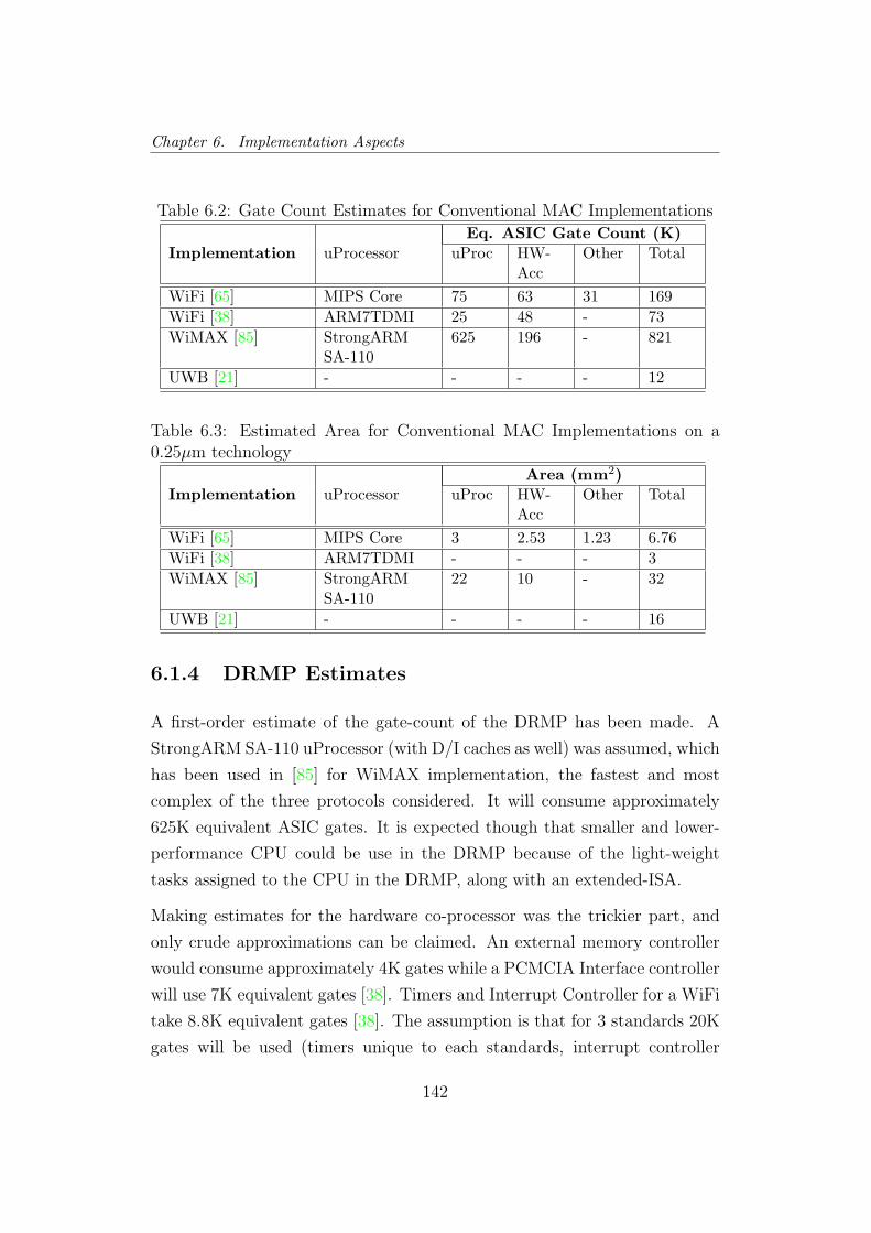
Chapter 6. Implementation Aspects
Table 6.2: Gate Count Estimates for Conventional MAC Implementations
Eq. ASIC Gate Count (K)Implementation uProcessor uProc HW-
AccOther Total
WiFi [65] MIPS Core 75 63 31 169WiFi [38] ARM7TDMI 25 48 - 73WiMAX [85] StrongARM
SA-110625 196 - 821
UWB [21] - - - - 12
Table 6.3: Estimated Area for Conventional MAC Implementations on a0.25µm technology
Area (mm2)Implementation uProcessor uProc HW-
AccOther Total
WiFi [65] MIPS Core 3 2.53 1.23 6.76WiFi [38] ARM7TDMI - - - 3WiMAX [85] StrongARM
SA-11022 10 - 32
UWB [21] - - - - 16
6.1.4 DRMP Estimates
A first-order estimate of the gate-count of the DRMP has been made. A
StrongARM SA-110 uProcessor (with D/I caches as well) was assumed, which
has been used in [85] for WiMAX implementation, the fastest and most
complex of the three protocols considered. It will consume approximately
625K equivalent ASIC gates. It is expected though that smaller and lower-
performance CPU could be use in the DRMP because of the light-weight
tasks assigned to the CPU in the DRMP, along with an extended-ISA.
Making estimates for the hardware co-processor was the trickier part, and
only crude approximations can be claimed. An external memory controller
would consume approximately 4K gates while a PCMCIA Interface controller
will use 7K equivalent gates [38]. Timers and Interrupt Controller for a WiFi
take 8.8K equivalent gates [38]. The assumption is that for 3 standards 20K
gates will be used (timers unique to each standards, interrupt controller
142

Chapter 6. Implementation Aspects
Table 6.4: Power Estimates for Conventional MAC Implementations
Power (mW)Implementation uProcessor uProc HW-
AccOther Total
WiFi [65] MIPS Core 98.4 91.5 73.1 263WiFi [38] ARM7TDMI - - - 100WiMAX [85] StrongARM
SA-110686 314 - 1000
UWB [21] - - - - 16
shared).
The physical interface for a WiFi implementation in reference [38] includes:
Tx and Rx state-machines, FIFOs, registers for access to an AMBA bus,
Tx and Rx DMA engine, Tx and Rx CRC and shift registers. It consumes
approximately 20K equivalent ASIC gates. The DRMP is designed to re-use
all of these resources for the 3 standards. But WiMAX will require more
resources for the same functions than a WiFi interface. The assumption is
that the reconfigurable interface (including a reconfigurable CRC) uses 40K
gates.
Now comes the most resource-consuming element of the Hardware Co-Processor—
encryption. RC4, DES, 3DES and AES are the encryption algorithms that to-
gether cover the three standards. Hamalainen et al. [27] gives figures for RC4
implementation using 255 CLBs of a Xilinx XC4000 device, which is 7.3K
equivalent ASIC gates. Pionteck et al. [68] discuss the implementation of
a reconfigurable AES implementation, and the complete Hardware/Software
partitioned implementation took 1.374mm2 on a 0.25um technology, which
approximates to 34K gates. From [95], it can be seen that a 3DES imple-
mentation uses 125% of an AES implementation. So one can approximate
it to consume 125% of 34K i.e. 43K gates. It may be assumed that a DES
encryption can be carried out on a parameterizeable 3DES implementation.
So if three encryption cores are implemented separately (RC4, 3DES and
AES), the gate count is appoximately 84K gates.
The reconfiguration overhead can only be guessed at this point. Pionteck
143

Chapter 6. Implementation Aspects
et al. [68] mention a reconfigurable AES encryption module in which area
overheads of reconfiguration logic and tables is 6.5%. For DRMP , the ap-
proximation is a 7% overhead of reconfiguration, in terms of both area and
gate usage. The power is also seen to be proportional. The percentage is
that of the Hardware co-processor, and not the whole SoC.
The interconnect is expected to consume a small fraction of the overall silicon
area (unlike an FPGA), and its contribution for a first-order estimate may be
ignored. All RFUs have not been taken into account, nor have the overheads
of interconnect. There is expected to be a control module for power and
clock management. A novel memory-manager that gives the RFUs access to
memory is also planned for this architecture. All these elements are assumed
to consume 20% more gates (See the entry for ‘others’ in the table).
Table 6.5 summarizes these results for the DRMP. It uses about 825K gates,
but note that the assumption is of a processor with Instruction/Data (I/D)
caches that uses 625K or 79% of that total area. The I/D caches in turn take
up a large proportion of the silicon in the uprocessor. If one just looks at the
Hardware co-processor, it consumes 200K gates, 8mm2 and may be expected
to consume around 260mW.
Component in the DRMP EstimatedGateUsage
Area inmm2
ApproximatePower(Watts)
Microprocessor 625 25 0.8125Memory Controller 4 0.16 0.0052Host Bus Interface 7 0.28 0.0091Timer and Interrupt Con-troller
20 0.8 0.026
PHY Interface (and CRC) 40 1.6 0.052Encryption Core 84 3.36 0.1092Reconfiguration Overheads 11 0.44 0.0143Others 34 1.36 0.0442DRMP Total 825 33 1.1
Table 6.5: Estimates for the DRMP.
Koushanfar et al. [48] mention typical die areas for mobile processors in the
144
Chapter 6. Implementation Aspects
year 2000 were between 22 to 154mm2. The estimated die area of the DRMP
of 33mm2 (for the complete HW/SW architecture) looks about right. The
figure for DRMP does not include resources for memories though and when
they are added the die area of the DRMP would be approaching the upper
limit of this range.
It is also relevant to discuss the effects of more current silicon technologies.
The estimates for DRMP have been made assuming a 0.25µm technology.
The silicon industry is has now advanced to using 40nm technology and
smaller. The relationship between the silicon technology scaling and the
power consumption per logic operation has been exponential until about
0.13 micron technology, according to [9]. However, while technology scaling
improves the active power consumption, it also increases the static leakage
current in the circuit. Beyond 0.13 micron, further scaling the dimensions
brings diminishing returns in terms of power consumption per logic operation
[9]. If we scale the DRMP to 0.13 µm technology, the power consumption for
the same DRMP device should decrease significantly, by almost 4–5 times
according to [9]. That means we can expect the DRMP device to consume
around 0.3 Watts or less on 0.13 µm technology. Scaling down to 40 nm
will decrease the power consumption even further, though not by the same
amount due to increased leakage currents.
6.2 Power-Efficiency Improvements
In section 5.5, it was discussed why the DRMP is expected to be more power-
efficient than an equivalent FPGA or software implementation. There are
some power-efficiency improvement techniques that suit the DRMP archi-
tecture and will improve the DRMP’s efficiency further. Note that these
are directly linked with the power modes of the MAC protocol themselves
(e.g. in WiFi and UWB) have sleep modes to conserve power. The focus
here is the optimization of power-efficiency beyond these protocol-specific
power-save modes.
145

Chapter 6. Implementation Aspects
60 80 100 120 140 160 180 200 220IDLE
BUSYA
BUSYB
BUSYC
MAC Microprocessor
60 80 100 120 140 160 180 200 220IDLE
BUSY
IDLE
BUSY
Task Handler for MAC Operations
60 80 100 120 140 160 180 200 220IDLE
BUSY
Reconfiguration Controller
60 80 100 120 140 160 180 200 220IDLE
BUSY
RFU for Defragmentation
60 80 100 120 140 160 180 200 220IDLE
BUSY
RFU for Decryption
60 80 100 120 140 160 180 200 220IDLE
BUSY
RFU for CRC
60 80 100 120 140 160 180 200 220IDLE
BUSY
RFU for Rx from PHY
60 80 100 120 140 160 180 200 220IDLE
BUSYA
BUSYB
BUSYC
Rx Buffer Interface with PHY (Actual Duration of Reception)
Simulation Time in Microseconds
Most of the modules in the hardware co-processor can be seen to be idle in these high-lighted portions
Figure 6.1: Activity Timing Diagram of Blocks in the DRMP Architecture(Packet Reception of 3 Modes) highlighting the time slack
Two important aspects of the DRMP architecture are relevant to this topic:
1. In section 5.4, the simulation results for the concurrent transmission
and reception of three protocol modes was presented. It was noted
that large parts of the architecture were idle even when three modes
run concurrently—a typical RFU was active for around 10% of packet
duration. It was also noted that when just one mode is active, which
one can expect to be the case for most of the time the device is being
146

Chapter 6. Implementation Aspects
used,the RFUs are typically busy for less than 5% to process a packet.
The time-slack available provides opportunity for power-optimization
techniques. Fig. 5.4 is reproduced here as Fig. 6.1 with the idle time
of various entities highlighted.
2. The DRMP’s hardware co-processor has a modular design with func-
tionality distributed in clearly partitioned functional units. These func-
tional units are designed such that they do not need to retain state
information across multiple uses—they are stateless and may be con-
sidered as hardware functions. Also, the RFUs in a non-active state do
not contribute to the interconnect network in any way4. The conclu-
sion I am driving towards is that when an RFU is not in use, it can
be powered-down without any loss of state-information or interconnect
throughput.
Standard low-power techniques like clock-gating, area optimization and mul-
tiple threshold voltage optimization optimization commonly used, and they
require little change in the architectural exploration, design, verification or
implementation stages. More advanced techniques like Dynamic Voltage and
Frequency Scaling (DVFS) and Power Shutoff (PSO) offer further power-
efficiency improvements, but have a higher methodology impact on the dif-
ferent stages of the SoC design.
From point 1, one can see an obvious solution for saving power; reduce the
clock frequency (the prototype model is simulated at 200 MHz). In section 5.5
in Fig. 5.5, it was shown that one could reduce the clock frequency to 50 MHz
while meeting real-time requirements. With a reduced clock frequency, a
lower voltage could also be used. However, since the DRMP aims to provide
flexibility to implement a variety of MAC protocols, one has to consider the
possibility that high bandwidth protocols could be deployed (In the prototype
model the three protocols have a bandwidth of 20 Mbps). Fixing the clock
4See [7] which describes a reconfigurable mesh architecture where the functional unitsnot only perform datapath operations but also act as router, passing data from one endto the other without processing.
147

Chapter 6. Implementation Aspects
frequency and voltage very low would render the DRMP suitable for faster
protocol standards.
Even if one fixes the clock frequency and voltage to be just fast enough for
the fastest protocol being implemented, the chip would waste power when
the other slower protocols are being executed.
The Dynamic Voltage and Frequency Scaling (DVFS) technique suitably ad-
dresses this problem. The frequency and voltage can be dynamically scaled
to accommodate the fastest protocol that is running at any time. If the user
switches to using a slower protocol, the frequency and voltage can be scaled
down so that the throughput is just enough for the slower protocol.
DVFS is a very effective and proven technique. It can reduce leakage power
by 2-3 times, and dynamic power by 40-70% [11, 82]. The timing and area
penalty is very little. It needs to be integrated into the design at the archi-
tecture design stage, and impacts the development process from the architec-
tural design stage through to design, verification and implementation. Since
the DRMP is still in the architectural design stage, it will be convenient to
integrate DVFS logic in the architecture.
Another exciting technique that could be used in the DRMP is Power Shutoff
(PSO). The RFUs in the DRMP are very well-suited for PSO techniques since
they do not need to retain state, and have no participation in the interconnect
network. It can reduce leakage power by 10-50 times [11, 82], and have very
little timing and area penalty. Vorwerk et al. [92] present a novel way of
using the PSO technique, reporting maximum net power savings of 61%.
This technique too requires integration from the onset of the architecture’s
design, which is not a problem for the DRMP architecture at its present
stage.
Note that even if one uses DVFS technique to dynamically scale the frequency
of the DRMP to as slow as possible, PSO could still be used to turn off power
to those RFUs in the DRMP that are not being used. At any one time in
the prototype model, a maximum of two RFUs are used. All the rest can
shut-off even if the clock frequency is just fast enough to process the packet
148
Chapter 6. Implementation Aspects
in time. In short, there is potential to use both DVFS and PSO techniques
simultaneously.
In section 6.1, the power consumption for the DRMP has been roughly esti-
mated without assuming any of these power saving techniques. In section 6.4,
this estimated power consumption of the DRMP is shown to be compara-
ble with commercial MAC solutions. The point to note is that according to
current estimates, even without these power saving techniques, the DRMP’s
power consumption is comparable to commercial devices. Hence the applica-
tion of these techniques is not a requirement to make the DRMP a feasible
solution for power-sensitive devices. However, these techniques will make the
DRMP a more attractive platform for power-conscious devices.
6.3 Utilization Potential and Limitations
The DRMP platform targets hand-held/portable devices - in other words
devices where power is an important consideration. For power-insensitive
devices, the more attractive option for incorporating flexibility is to imple-
ment the MAC entirely in Software or an FPGA.
It is meant to target multi-standard hand-held devices that need to deal
with multiple wireless standards at the same time. Such devices are al-
ready present in the market and the trend is towards greater integration of
standards in a single device. Eventually, this platform could be used for
Software-defined radios. But that is not the main target and so the unique
considerations associated with SDR’s were not addressed in the project.
It is also meant to address the wireless protocols that can be typically ex-
pected in consumer devices. So WiFi, Bluetooth, WiMAX are the protocols
that will be targeted. Protocols like Zigbee which are not designed for con-
sumer devices were not considered. The reason for aiming at consumer de-
vices is that these devices tend to be produced at massive scales and in such
scenarios it becomes possible to justify a domain-specific hardware platform.
Having run simulations involving transmission and reception of packets of
149
Chapter 6. Implementation Aspects
three different protocol modes concurrently, the results have confirmed that
the processing of packet on the DRMP architecture takes a fraction of the
actual duration of the packet (See table 5.1 on page 126).
In section 5.5, these results were discussed, where it was seen that the DRMP,
clocked at 200 MHz, manages to process the transmission and reception of
three packets simultaneously at data rates of 20 Mbps—yet the functional
units remain idle for more than 90% of the time. The power-saving oppor-
tunities offered by this time-slack and the limited interconnect requirement
in the hardware co-processor were also discusssed. In section 6.1, the power-
consumption of the DRMP was estimated, without using any power-saving
techniques that were discussed in section 6.2.
With these results, there is effectively a proof-of-concept that the DRMP can
replace up to three MAC processors in a hand-held device. This should make
it a attractive SoC IP for the hand-held device market in one the following
contexts:
• an IP on another higher-level SoC
• a chip on a System-in-Package (SiP) or
• a packaged chip on a PCB — though considering the form factor of the
target devices, this option is unlikely.
The potential customer thus could either be a chip manufacturer or a device
manufacturer. The possible considerations of an expected customer looking
to use this IP in one of the above scenarios will now be discussed, along with
where the DRMP stands at present in view of these considerations.
6.3.1 Power-Efficiency
The tool used to model the DRMP (Simulink), and the way its been used
(abstract functionality, relatively exact timing) imply that only a crude first-
order estimation of power and area expected to be used by the DRMP, can
150
Chapter 6. Implementation Aspects
be made. It should be noted though that the DRMP is not an attempt to
optimize the power-efficiency or gate-count. It aims to provide the flexibility
needed to incorporate multiple MACs in a single device, while keeping the
power-efficiency acceptable for a hand-held device. That is to say, the aim
is to keep the power consumption below a certain threshold of acceptance
for hand-held devices; and certainly less than that of the architectures tra-
ditionally used where flexibility is required e.g. microprocessors or FPGAs.
Table 6.5 gives the first order estimates of gate count and power consumption.
A 0.25um technology and operating frequency of 85 MHz is assumed for
estimating the power consumption. It was found that the first-order estimate
of die area was within acceptable range for mobile devices.
In brief, the first order calculations indicate that the DRMP will indeed be
suitable for power and resource sensitive hand-held devices. But some effort
to get more accurate estimates would be in order before committing more
resources to this architecture’s further development.
6.3.2 Performance
Performance here means the throughput—how fast can the DRMP process
packet data. The aim is simply to achieve throughput above a certain
threshold—the real-time throughput requirements imposed by the protocol.
Once that threshold is crossed, nothing is gained by further improvements
in the performance. Fortunately, because of the cycle-approximate model
of the DRMP, it is quite straightforward to decide if the DRMP is meeting
the timing requirements of the protocol. Results from the prototype model
indicate that the DRMP will comfortably meet the throughput requirements
of the protocols being considered even when running at a moderate 200 MHz
operating frequency and processing three protocol data streams at 20 Mbps
concurrently.
151
Chapter 6. Implementation Aspects
6.3.3 Cost
The DRMP, if it is to be commercialized, will involve the complete design,
synthesis and fabrication of a SoC, and hence the cost will be in the order
of millions of dollars. It is however targeting a mass-market of consumer
hand-held devices which includes mobile phones, smart phones, PDAs and
laptops etc. If the DRMP is used by a fraction of device manufacturers in
this market for implementing the MAC layer on their devices, one is easily
looking at a figure of millions of chips per year. If the DRMP is used by
even one mainstream wireless consumer device manufacturer, the economies
of scale would bring the price tag to an acceptable value.
6.3.4 Programmability and Extensibility
It is important to note that DRMP is planned to be configurable at two
distinct levels. One is the dynamic, on-the-fly reconfiguration for concurrent
multi-mode operation on a device. This aspect of DRMP’s configuration has
been the focus of this research, and it is at this level that the current results
are very significant. The other level of configuration is the DRMP’s ability to
evolve or change functionality over time to incorporate other protocol MAC
functionalities in the same hardware IP. This is the future-proofing aspect of
this architecture. Further research needs to be done to elevate the DRMP
from a 3-MAC-protocol specific architecture to a more general purpose MAC
processor, as discussed in section 4.3.
In terms of the DRMP’s programmability, the current model meets an im-
portant requirement of a flexible, future-proof device. Among other things,
to make an architecture flexible and future-proof, it needs to have high-level
programmability. In context of the MAC layer, the designers need to meet
very strict time-to-market constraints in the fast evolving world of wireless
standards. That the DRMP is domain-limited results in a very simple API
for it. The functional units in the DRMP, in the prototype at least, are flex-
ible but function-oriented; i.e. the hardware elements are closely matched
152

Chapter 6. Implementation Aspects
to the intended functionality. Configuring them does not require a general-
purpose programming paradigm like RTL design in an HDL. The way the
RFUs have been partitioned, it is expected that in most cases, all it would
take to configure an RFU to make it work with a new protocol would be
the loading of some parameters. In the prototype, in which three protocols
are expected to be implemented, a simple function call is all that is required
for an microprocessor to access the resources offered by the flexible hard-
ware co-processor. Any reconfiguration required is done automatically by
the hardware co-processor. No other programming of hardware is needed.
It should be noted that the DRMP’s prototype is designed to be extensible
by third-party system and hardware designers. The reconfigurable functional
units (RFUs) in the DRMP, which do all the MAC operations partitioned to
hardware, have a well-defined interface. They are not homogeneous, but they
are clearly categorized into a number of classes, and their hence their interface
for carrying out a function as well as reconfiguration is well-defined. It will
thus be relatively straightforward for a third-party to extend the DRMP
by designing their own RFUs and integrating them into the Hardware Co-
Processor in the DRMP.
6.4 Commercial Wireless MAC solutions
In this section, some commercial implementations of wireless protocols for
consumer devices are discussed. Commercial device manufacturers give out
limited information about their architectures and power consumption and
area figures. The information available is typically given for the complete
MAC + PHY implementation. From these figures the usage for MAC im-
plementations can be loosely approximated. Also note that the estimates for
the DRMP architecture are at best indicative, as calculated and discussed
in section 6.1. The purpose though is to give an idea of the practicality of
the DRMP architecture in view of its power consumption relative to other
devices implementing MAC layers, and for this purpose such a comparison
suffices.
153

Chapter 6. Implementation Aspects
The estimates we have calculated for the DRMP assume it is being used for
WiMAX as well as the other two smaller protocols. The DRMP cannot be
compared with a single protocol solution of any of these protocols, but the
comparison is even more unrealistic for single protocol solution for WiFi and
Bluetooth. To make a realistic comparison, it is compared with a hypothet-
ical multi-standard device where all three protocol MACs are implemented
separately.
Cambridge Silicon Radio (CSR) is a company based in Cambridge, Eng-
land, and their products include single-chip implementations of Bluetooth
and Wifi. The BlueCore is a single-chip solution for Bluetooth5 including a
RISC processor, and aimed at low-power devices. The latest device in the
range is BlueCore7. It has an active power consumption of 19mW [16]. It is
a complete Bluetooth stack solution6.
CSR also have a single-chip solution for WiFi, UniFi. This solution is tar-
geted at low-power devices. In this product family, UniFi UF1050 device
implements 802.11b/g for application in handheld devices. It is fabricated
on 0.13 micron CMOS. It provides Dual 60 MHz RISC processors, one for
MAC and one for PHY, and accelerators for Encryption and other MAC
functions. Power consumption or area figures are not available.
Intersil Corp. has been involved in solutions for WiFi in all its versions, and
has been a major producer in the WiFi market [23]. Its Prism architecture
(now maintained by Conexant) implements both the MAC and PHY layers.
In transmission mode, the Prism 1 device consumes 488 mA (2.4W at 5V)
5Although we have investigated the MAC layer of IEEE 802.15.3 WPAN for the DRMP,it was never commercialized. Hence, for making comparison with commercial devices,Bluetooth solutions have been investigated since Bluetooth is a widely commercializedWPAN protocol.
6To estimate the MAC power consumption, we need an approximate figure for theproportional contribution of MAC to the total MAC + PHY solution in terms of com-putational requirement (MIPS) and power consumption. A complete WiFi solution at 12Mbps requires 5500 MIPS. Of this, approximately 4500 MIPS are required for the PHYlayers [19], hence about 1000 MIPS for the MAC. An approximate 1000 MIPS require-ment for the WiFi MAC layer can also be inferred from [65]. Therefore, for the MAClayer, an approximate 20% utilization of the total power consumption of the MAC + PHYintegrated solution is a reasonable assumption. We will use this approximation for all thewireless protocol solutions considered in this section.
154

Chapter 6. Implementation Aspects
Figure 6.2: High-level block diagram of Sequans SQN1010 WiMAX SoC(Reproduced from [81])
[41] when it is actively transmitting.
Conexant’s CX53121 is a single-chip solutions for WiFi, targeted at small
form factor mobile applications. The MAC is implemented in an ARM9
processor. The device includes Conexant’s PowerSave technology, which pro-
vides intelligent power control, and results in a deep sleep current in the order
of 10 microamps. Active power consumption figures were not available.
Sequans Communications have designed an integrated MAC/PHY SoC so-
lution for WiMAX subscriber stations. The MAC implementation is parti-
tioned between hardware and software. The software is implemented on an
ARM9 processor. The power consumption is up to 2W [81]. Fig. 6.2 is a
high-level block diagram of the SQN1010 SoC, where it can be seen that the
MAC implementation is accelerated in a separate hardware block.
Fujitsu Microelectronics Inc. have also developed an integrated MAC/PHY
SoC solution, MB87M3400, for WiMAX base stations and subscriber sta-
tions. It has dual RISC processors for implementing upper and lower MAC
layer functions. The upper MAC layer processing is done by an ARM9 pro-
cessor, while the lower MAC layer processing is done on an ARC processor
155

Chapter 6. Implementation Aspects
Figure 6.3: Block Diagram of the Fujitsu MB87M3400 Integrated SoC solu-tion for WiMAX MAC/PHY (Reproduced from [25])
[25]. Power consumption can be up to 6W [57]. Fig. 6.3 is a simplified block
diagram of the MB87M3400 SoC, showing the two RISC processors and the
hardware blocks that together provide the WiMAX solution.
Intel has been a major force behind the adoption of WiMAX. One of its
WiMAX solutions is the WiMAX connection 2250 [40]. This product too is
an integrated SoC solution. Two ARM9 processors are used for PHY, MAC
and application protocol processing. Power consumption figures for this SoC
were not available. Fig. 6.4 is a block diagram of the WiMAX connection
2250 SoC.
Intel IXP1200 Network Processor also makes an interesting comparison. It
is a software programmable device that has a StrongARM core and six in-
tegrated “Programmable Microengines” that can access the SRAM and the
DMA channels. It also has other integrated hardware peripherals geared
towards packet-processing applications. It can be used in a wide variety
of LAN and telecommunications products. Typical power consumption is
5.19W [39]. Fig. 6.5 is a block diagram showing the StrongARM core, the
six programmable microengines, and other peripherals.
While there are many other devices that could be used for comparison, the
above mentioned suffice to indicate the trend in the commercial sector in
context of wireless MAC solutions, in context of their high-level architec-
ture, as well the power typically consumed by these commercial devices. In
156

Chapter 6. Implementation Aspects
Figure 6.4: Intel WiMAX Connection 2250 SoC (Reproduced from [40])
Figure 6.5: Intel IXP 1200 Network Processor (Reproduced from [39])
Table 6.6, this information is tabulated, and then compared with the DRMP
in terms of power consumption. While the figures for DRMP are based on a
0.25µm technology, the technology for all of the commercial devices listed is
157
Chapter 6. Implementation Aspects
not available, which is a limitation of this comparison.
We can see that the DRMP MAC processor consumes approximately the
same amount of power as a hypothetical multi-standard MAC solution we
have constructed from three commercial devices. If we consider that the
DRMP is programmable for other MAC protocols, while the hypothetical
multi-standard solution is limited to three specific MAC protocols, we can
conclude that DRMP should be feasible for commercial consumer devices.
Limitations of Comparison
The complete life-cycle of the the development of an SoC architecture re-
quires many times more effort than is possible in a single doctorate project.
The DRMP in its current shape can be considered to be an SoC in its in-
fancy. There are hence short-comings in the architecture—and consequently
its power estimates and its comparison to commercial devices—that can be
addressed through further research and development until it becomes an IP
ready for commercial usage.
A key issue that was felt to be unaddressed, is further investigation, modeling
and implementation of RFUs that are suitable for a certain set of protocols.
While this topic is addressed in this dissertation, it is realized that the current
depth of investigation in this avenue is not satisfactory from the point of
view of a designer who would want to judge the suitability of using this
architecture.
Lack of synthesis results and concrete estimates of power and area is another
shortcoming that can be addressed by designing the RTL for the architecture.
While some design aspects have been investigated in some detail, like the
design of the Interface and Reconfiguration Controller, other aspects of design
like the interconnect, the memory-architecture, extended-ISA for the CPU
etc have considerable room for investigation and optimization.
158
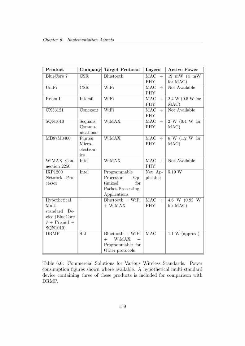
Chapter 6. Implementation Aspects
Product Company Target Protocol Layers Active PowerBlueCore 7 CSR Bluetooth MAC +
PHY19 mW (4 mWfor MAC)
UniFi CSR WiFi MAC +PHY
Not Available
Prism I Intersil WiFi MAC +PHY
2.4 W (0.5 W forMAC)
CX53121 Conexant WiFi MAC +PHY
Not Available
SQN1010 SequansCommu-nications
WiMAX MAC +PHY
2 W (0.4 W forMAC)
MB87M3400 FujitsuMicro-electron-ics
WiMAX MAC +PHY
6 W (1.2 W forMAC)
WiMAX Con-nection 2250
Intel WiMAX MAC +PHY
Not Available
IXP1200Network Pro-cessor
Intel ProgrammableProcessor Op-timized forPacket-ProcessingApplications
Not Ap-plicable
5.19 W
HypotheticalMulti-standard De-vice (BlueCore7 + Prism I +SQN1010)
– Bluetooth + WiFi+ WiMAX
MAC +PHY
4.6 W (0.92 Wfor MAC)
DRMP SLI Bluetooth + WiFi+ WiMAX +Programmable forOther protocols
MAC 1.1 W (approx.)
Table 6.6: Commercial Solutions for Various Wireless Standards. Powerconsumption figures shown where available. A hypothetical multi-standarddevice containing three of these products is included for comparison withDRMP.
159

Chapter 7
Conclusions
Devices capable of wireless communication have become a part of our ev-
eryday lives. As consumers, our expectations have steadily kept growing,
with the industry responding by bringing out newer protocols and devices.
In the near future, commercial software-defined radios will replace the multi-
standard handsets that are already available and one can then expect to
see commercialization of cognitive radios. Reconfigurable computing is re-
garded as the key enabling technology that will enable such devices to be
widely available to consumers at affordable prices and with good battery
lives. Wireless communication protocols, hand-held devices and reconfig-
urable technologies were reviewed. Using these discussions, a case was built
for the architecture of the DRMP platform.
The DRMP is an innovative coarse-grained dynamically reconfigurable system-
on-chip architecture. It is not a device looking for a killer application, but
is an architecture that is designed around and specialized for the Wireless
MAC layer, and aimed at a specific market of consumer hand-held devices.
The DRMP allows reconfiguration dynamically on a packet-by-packet basis
for three protocols. The hardware co-processor has coarse-grained, hetero-
geneous, function-specific reconfigurable processing units. There is a clear
partition of datapath logic to the hardware co-processor, such that the CPU
never directly handles the packet data, and is only left to perform the pro-
160

Chapter 7. Conclusions
tocol control operations.
The project has spanned across a wide range of issues since it essentially deals
with the architectural design of a complete System-on-Chip. Knowledge of
various subjects like:
• reconfigurable computing,
• interconnection,
• memory design,
• Hardware / Software co-design,
• MAC protocols,
• power-saving techniques,
• parallel computing
were an important part of the project. However, this project as-such does not
advance the state of the art in these areas. It is more of a bringing together
of various technologies for a specific purpose. The resulting design is unique
and innovative, and I believe it can make a very important contribution in
the area of multi-standard wireless consumer devices. It is in this area where
I feel the state of the art has been advanced in this project. More specifically,
five cornerstones of the project which make it innovative have been identified
:
1. Exploitation of similar functionality of MAC Layers of various wireless
standards.
2. Heterogeneous, function-specific, reconfigurable functional units.
3. Use of dynamic and partial reconfiguration for implementing MAC
functions.
161

Chapter 7. Conclusions
4. An interface and reconfiguration control that enables transparent use
of a dynamically reconfigurable hardware for running three parallel
protocol contexts, reconfiguring the hardware co-processor packet to
packet.
5. A CPU that has only the MAC protocol control to implement, and a
interrupt-driven programming model that handles three protocol con-
trol on a single CPU.
A Simulink model and results of simulation runs involving concurrent trans-
mission and reception of packet of different protocols was presented. From
the results, it has been shown that the DRMP is more than capable of meet-
ing the protocol timing requirements even though it shares the hardware
resources amongst the three protocol modes, and dynamically reconfigures
the functional resources on every packet. This performance is achieved at
a modest 200MHz clock, and yet leaves considerable time-slack that can be
used for getting more power-efficiency than the coarse-grained and hetero-
geneous nature of the DRMP inherently offers. Re-using the DRMP for
different protocols through a simple API would reduce development risks,
costs and time to market.
The DRMP is by all means an innovative and unique architecture, designed
with the consumer hand-held device in mind. It has been made to meet
the challenges that the consumer hand-held industry places on wireless so-
lution designers; flexibility, power-efficiency, performance, programmability
and future-proofing. From the knowledge about the architecture’s poten-
tial from its prototype model and related investigation, it appears to be a
very promising device with potential to find its place among handset and chip
manufacturers in the consumer wireless market. There are however still some
unknowns and further research and investigation is needed before designers
and manufacturers will become seriously interested in it.
162

Chapter 7. Conclusions
7.1 Future Architectural Exploration
There is tremendous room for research and development on this architecture.
The DRMP is fundamentally unique and innovative architecture. While in
context of this dissertation the research work on the architecture is complete,
the architecture can still be considered to be in its infancy, and has some way
to go before it can be realized in silicon. It needs work in two main areas:
System Design and Synthesis.
7.1.1 System Design or Architectural Exploration
The basic architecture of the DRMP is in place in the current prototype,
designed at an abstract level. But even at this abstraction, further refine-
ment needs to be made. More specifically, the following areas need further
exploration:
Design of RFUs The RFUs are heterogeneous, to be designed keeping in
view the overlapping as well as distinct functionalities of the various
MAC protocols considered. The RFUs currently are modeled at high
abstraction and some with dummy functionality, aimed mostly at the
802.11 WiFi MAC. Focus has mostly been on their interaction, recon-
figuration and topology. There is an avenue of research open where
RFUs optimal for the WiFi as well as other chosen MAC protocols
would be designed, with the aim to achieve the optimum balance of
power-efficiency / resource-usage and flexibility. This R&D work is
essential to take the DRMP from concept to a real, usable IP.
Memory Architecture Although the DRMP prototype clearly partitions
the various memory elements used in the hardware co-processor, these
memories are modeled at a high abstraction without detailing their
technology, sizes, or access characteristics. These are not the kind of
unknowns though that will need a extensive innovative research to be
quantified. It can be expected be a relatively straightforward engineer-
ing task.
163
Chapter 7. Conclusions
Interconnect The interconnect in the Hardware Accelerator of the DRMP
is currently modeled as a simple bus-based mechanism, albeit with some
unique characteristics. Although it is a feasible option, it has not been
investigated and identified as the optimal solution. More research in
this area could yield a better interconnect design that can e.g. provide
the same interconnect throughput while using fewer resources.
Power-Efficiency Improvement Techniques The fact that the hardware
functional units are idle for large proportion of the packet duration,
along with the modular partitioning of the DRMP leaves considerable
room for employing power-improvement techniques. Results of brief in-
vestigation have been presented in section 6.2 Further research in this
area should result in making the DRMP a more attractive option for
power-sensitive hand-held devices.
From a 3-protocol Specific to a General-purpose MAC Architecture
This was discussed earlier in the section 4.3 where the evolution of
DRMP as a platform architecture is presented. This is probably the
most exciting and potentially innovative area of research open from
this point on. If it can eventually be shown that the DRMP can: im-
plement the MAC layer functionality of most if not all the prevalent
wireless protocols, do it at acceptable power consumption, provide a
simple API, and run up to any of these 3 (or perhaps more) protocols
in parallel, then there is a very strong case for commercializing the
DRMP.
Other Application-Domains Although this architecture is aimed at the
MAC-layer domain, there is nothing in the architecture that would limit
it to this domain only, apart from the choice of RFUs. It would be very
interesting to explore other application domains where a heterogeneous,
domain-specialized device, offering limited flexibility at improved effi-
ciency, may be feasible.
164
Chapter 7. Conclusions
7.1.2 Synthesizing the Architecture to Lower Abstrac-
tion
Once a stable high abstraction model is complete, the next step would be
to synthesize it to lower abstraction for two reasons: First, to confirm the
timing and area estimates and thus establish the viability of the architecture.
Secondly, the more obvious reason get an actual implementation in silicon,
or at least a synthesizable soft IP, to be able to sell it to handset and chip
manufacturers.
The current abstraction level of the DRMP model should make the synthesis
exercise a relatively straightforward, engineering task. The timing accuracy
of the DRMP model should give enough detail to the RTL designer so as
to make the RTL design a simple development task, rather than a research
effort.
In addition to the future exploration avenues discussed above, there are some
ideas that are very interesting and will make this architecture attractive for
manufacturers of handsets and portable devices. These ideas mostly deal
with using an already available technology in the context of this reconfig-
urable MAC processor. Use of power islands e.g. is an attractive option
in this sharply partitioned hardware architecture where power to functional
units not being used can be switched off. The concept of dynamic voltage
and frequency scaling of microprocessors is very relevant in this context too.
Another idea that was found to be appealing was the use of a software-based
universal low-performance backup functional unit that sits in the hardware
and caters for unforeseen functions in future standards that have no corre-
sponding hardware functional unit. Such a feature on top of the discussed
architecture of the DRMP will make it very flexible and perhaps even a
universal MAC platform that is power-efficient enough for portable devices.
With the extensive proliferation of multi-standard portable devices, such a
platform can be very attractive to handset manufacturers.
165
Appendix A
Snapshots of SIMULINK
Model
Mathwork’s Simulink modeling environment has been used for a prototype
model of the DRMP architecture. The Stateflow toolbox has been used to
model control logic in the model.
The chapter on system architecture contains block diagrams of the various
parts of the architecture. Here some snapshots of the actual model’s various
hierarchical levels are included. While this is just a model for simulation,
the interesting thing to note is how modeling in Simulink exposes the hierar-
chical structure of the architecture, the interconnect arrangement, and also
indicates the actual topology of various blocks.
The snapshots are not exhaustive. They are chosen to represent the different
techniques used to model the various parts of the DRMP SoC in the Simulink
environment. The rest of the snapshots are very similar to the ones presented,
and hence not produced.
166
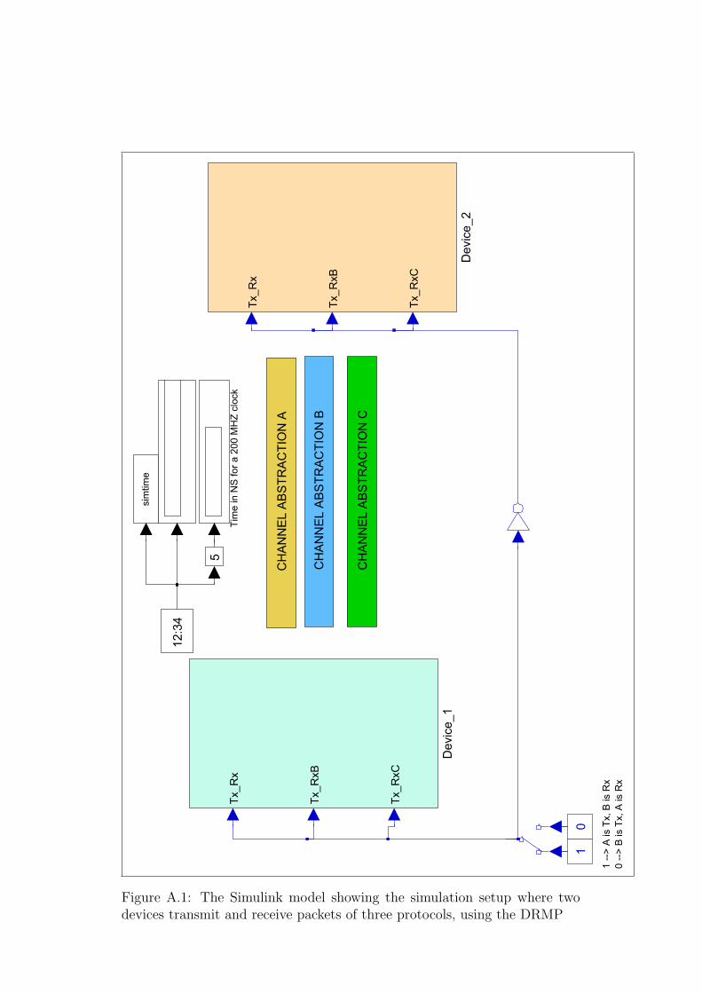
Tim
e in
NS
for a
200
MH
Z cl
ock
1 --
> A
is T
x, B
is R
x0
-->
B is
Tx,
A is
Rx
Dat
aRdy
CTo
pSiz
eCTo
pDat
aC
Dat
aRdy
BTo
pSiz
eBTo
pDat
aB
Dat
aRdy
ATo
pSiz
eATo
pDat
aA
sim
time
5
12:3
4
Dev
ice_
2
Tx_R
x
Tx_R
xB
Tx_R
xC
Dev
ice_
1
Tx_R
x
Tx_R
xB
Tx_R
xC
01
CH
AN
NE
L A
BS
TRA
CTI
ON
C
CH
AN
NE
L A
BS
TRA
CTI
ON
A
CH
AN
NE
L A
BS
TRA
CTI
ON
B
Figure A.1: The Simulink model showing the simulation setup where twodevices transmit and receive packets of three protocols, using the DRMP

dbg_
rfu8
dbg_
rfu7
dbg_
rfu6
dbg_
rfu5
dbg_
rfu3
dbg_
rfu2
DE
VIC
E_I
D
dbg_
bus
dg_t
hr3
dg_t
hr2
dg_t
hr1
dg_t
hm3
dg_t
hm2
dg_t
hm1
dbg_
rxbu
f_pi
Cdb
g_rx
buf_
piB
dbg_
rxbu
f_di
C
IF_r
eg_A
PP
uP
dbg_
rxbu
f_di
B
dbg_
txbu
f_pi
Cdb
g_tx
buf_
piB
dbg_
rxbu
f_pi
Adb
g_rx
buf_
diA
dbg_
txbu
f_di
Cdb
g_tx
buf_
diB
dbg_
txbu
f_pi
Adb
g_tx
buf_
diA
dbg_
rfu1
pmem
_end
addr
_apr
oc
pmem
_sta
rtadd
r_ap
roc
pmem
1
Buf
fer_
Des
cCB
uffe
r_D
escB
hwre
g0
hwre
g4
hwre
g3
hwre
g2
hwre
g1
Buf
fer_
Des
cA
{CLK
}
Wifi
_PH
YC
PhyIF_ds
Tx_RxPhyIF_us
Wifi
_PH
YB
PhyIF_ds
Tx_RxPhyIF_us
Wifi
_PH
YA
PhyIF_ds
Tx_RxPhyIF_us
Tx_R
xA1
pmem
1
Rec
onf_
HW
_Acc
MA
Cup
_bus
Hos
t_bu
s
Phy
IF_u
sA
Phy
IF_u
sB
Phy
IF_u
sC
int2
sw
Phy
IF_d
sA
Phy
IF_d
sB
Phy
IF_d
sC
Pcl
ock_
genpc
lkA
pclk
B
pclk
C{P
CLK
C}
{PC
LKB
}
{PC
LKA
}
MA
cup_
Mem
ory
Tr mas
ter_
busdo
ut
MA
C_S
oftw
are
int2
swA
MA
Cup
_bus
INT2
AP
PuP
Inve
rt_C
onve
rtBoo
l
In1
Out
1
IF R
EG
Tab
le
DO
C Text
Hos
t_M
emor
y
Tr
Host_bus
dout
HB
_Arb
A_i
M_i
Hb
{HM
_do}
{MM
_do}
{PM
_ad1
}
{MU
Dr}
{PC
LKC
}{P
CLK
B}
{MU
Di}
{dbg
_irc
_th3
_thr
}
{RC
_EN
_8}
{RC
_EN
_6}
{RC
_EN
_5}
{RC
_EN
_3}
{RC
_EN
_7}
{RC
_EN
_2}
{RC
_EN
_1}
{dbg
_irc
_rcn
tr}
{dbg
_irc
_th1
_thr
}
{MU
DSi
}
{dbg
_irc
_th1
_thm
}
{dbg
_mac
proc
}
{RD
ON
E8}
{RM
_ad8
}
{DO
NE8
}
{PM
_di8
}
{PM
_ad8
}
{PM
_wr8
}
{PC
LKA
}
{dbg
_irc
_th2
_thr
}
{MM
_do}
{RM
_ad7
}
{PM
_di7
}
{PM
_ad7
}
{PM
_wr7
}
{RD
ON
E7}
{DO
NE7
}
{RM
_ad6
}
{PM
_di6
}
{PM
_ad6
}
{PM
_wr6
}
{DO
NE3
}
{RD
ON
E6}
{DO
NE6
}
{RM
_ad5
}
{PM
_di5
}
{PM
_ad5
}
{PM
_wr5
}
{RD
ON
E5}
{DO
NE5
}
{RM
_do}
{RM
_ad3
}
{DO
NE2
}
{RM
_ad2
}{R
M_a
d1}
{RD
ON
E3}
{RD
ON
E2}
{RD
ON
E1}
{dbg
_irc
_th3
_thm
}{d
bg_i
rc_t
h2_t
hm}
{PM
_wr4
}{P
M_w
r3}
{PM
_wr2
}
{DO
NE1
}
{PM
_wr1
}
{PM
_do2
}{P
M_d
o}
{PM
_di4
}{P
M_d
i3}
{PM
_di2
}{P
M_d
i1}{P
M_a
d4}
{PM
_ad3
}{P
M_a
d2}
{CLK
}
{HM
_do}
{CLK
}
{CLK
}
Deb
ugTx
Deb
ugR
x
pmem
1
01
DM
A
bi bo
App
_Pro
cess
or
INT1
Tx_R
x
Hos
t_bu
s
VIS
IBIL
ITY
TA
GS
FO
R S
CO
PIN
G
Tx_R
xC3
Tx_R
xB2
Tx_R
x
1
Hos
t_bu
s
Figure A.2: The device model showing the DRMP along with the Applicationprocessor, the memories, and PHY layer models. The highlighted block inthe center is the DRMP, showing the CPU and the Hardware Co-Processor
168

eM
R
eque
st_R
HC
P_S
ervi
ce(P
mod
e, C
omm
and,
AR
G1,
AR
G2,
AR
G3,
AR
G4,
AR
G5,
AR
G6,
AR
G7)
IDLE
/en
: tr_
rha
= 0;
eM
R
eset
_IF_
RE
GIS
TER
S
eM
y =
calc
_fra
grem
(siz
e, th
resh
old,
hea
der_
size
) e
M y
= ca
lc_f
ragt
otal
(siz
e, th
resh
old,
hea
der_
size
)
Sta
tic_C
onfig
_Mod
eA
eM
D
ON
E =
Int_
Han
dler
_Mco
de_A
Sta
tic_C
onfig
_Mod
eB
Sta
tic_C
onfig
_Mod
eCW
AIT
4int
erru
pt
Int_
Han
dler
_BIn
t_H
andl
er_C
Int_
Han
dler
_A
/*D
o st
artu
p st
atic
conf
igur
atio
n fo
r mod
e A
here
*/
/*D
o st
artu
p st
atic
conf
igur
atio
n fo
r mod
e B
here
*/
/*D
o st
artu
p st
atic
conf
igur
atio
n fo
r mod
e C
here
*/
clk
[int2
swA
==
1]1
clk
[int2
swC
==
1]2
{dbg
_mac
proc
= 1
}cl
k [in
t2sw
B =
= 1]
/ {d
bg_m
acpr
oc =
2}
3{d
bg_m
acpr
oc =
3}
{tr_r
ha =
0}
{tr_r
ha =
0}
{tr_r
ha =
0}
{tr_r
ha =
0}
{tr_r
ha =
0}
{tr_r
ha =
0}
{dbg
_mac
proc
= 0
}
Figure A.3: The stateflow chart showing the interrupt-driven protocol controlof the three protocols. The Interrupt-handlers are implemented in matlab-code.
169

PM
Acc
ess
Bus
To u
PFr
om u
P
Rec
onf C
ontro
l Bus
Clo
ck T
ree
RFU
_DO
NE
_BU
S
RO
M
BU
S R
EQ
UE
STS
BU
S R
EQ
UE
STS
<---
----
----
- I/F
to th
e P
HY
laye
r ---
----
----
-->
Phy
IF_d
sC4
Phy
IF_d
sB3
Phy
IF_d
sA2
int2
sw1
reco
nf_m
em
Tr RM
_busdo
ut
reco
nf_b
us_a
rbite
r
Rbu
s_R
eq
reco
nf_b
us
Rbu
s_G
rnt
pack
et_m
em
Tr PM
_bus
PM
_bus
2
dout
dout
2
pack
et_b
us_a
rbite
r
Pbu
s_R
eq
pack
et_b
us
Pbu
s_G
rnt
deco
der
bibo
BU
S_G
RN
T_O
RID
E
IRC
_ID
PM
_RFU
_NO
PM
_RFU
_BA
SE
US
arbi
ter
Abu
sB
bus
Cbu
sO
bus
TxR
xBuf
fers
_Mod
eC
DR
MP
_ds
PH
Y_I
nt_u
s
DR
MP
_us
PH
Y_I
nt_d
s
TxR
xBuf
fers
_Mod
eB
DR
MP
_ds
PH
Y_I
nt_u
s
DR
MP
_us
PH
Y_I
nt_d
s
TxR
xBuf
fers
_Mod
eA
DR
MP
_ds
PH
Y_I
nt_u
s
DR
MP
_us
PH
Y_I
nt_d
s
ToB
uses
_4
pmem
_bus
RFU
_Trig
ger_
Logi
c
PB
US
RFU
_Cnt
rl
RFU
_Poo
l
RB
US
CO
NTR
OL
CLK
PM
_BU
S
RM
_BU
S
Phy
IF_u
s
Phy
IF_d
s
RC
_IC
_abs
tract
ion
rc_r
fu_c
nfgs
t
rc_r
fu_i
d
rc_r
en
RC
_Bus
I_R
_Con
trolle
r
host
_bus
EH
_tr_
rha
clk
RFU
_DO
NE
RFU
_RD
ON
E
Pbu
s_G
rnt
Rbu
s_G
rnt
PM
_BU
S
int2
sw
rc_r
fu_c
nfgs
t
rc_r
fu_i
d
rc_r
en
Rbu
s_R
eq
Pbu
s_R
eq
PM
_BU
Si
{PM
_do}
{PM
_do2
}
{RM
_do}
{CLK
}
Eve
nt_H
andl
er
clk
Phy
IF_u
sAP
hyIF
_usB
Phy
IF_u
sCtr_
rhaD
ON
E_L
OG
IC
DO
NE
Phy
IF_u
sC5
Phy
IF_u
sB4
Phy
IF_u
sA3
Hos
t_bu
s
2
MA
Cup
_bus
1
<RD
ON
E>
dout
_pm
em
dout
_rm
emR
M A
cces
s B
us
RM
Acc
ess
Bus
Figure A.4: Inside the RHCP sub-system in the model. IRC, RFU pool,Interface Buffers, Memories, Arbiters and Interconnect can be seen.
170

PM
_BU
Si
7
Pbu
s_R
eq6
Rbu
s_R
eq5
rc_r
en4rc
_rfu
_id
3rc
_rfu
_cnf
gst
2
int2
sw1
rfu_t
able
rfut_
bus
rfu_i
do
nsta
tes
narg
s
c_st
ate
in_u
se
Qre
q1
PrQ
req1
Qre
q2
PrQ
req2
op_c
ode_
tabl
e
op_code
nargs
rfu_id
recon_st
recon_vec
{dbg
_irc
_th3
_th
{dbg
_irc
_th2
_th
{dbg
ircth
3th
m{d
bgirc
th2
thm
{dbg
_irc
_th1
_thm
{dbg
_irc
_rcn
tr}
{dbg
ircth
1th
Ass
ign2
RC
_oct
IC_o
p_in
RC
_op_
inop
c_ou
t
Ass
ign2
RC
IC_b
us_i
n
RC
_bus
_in
bus_
out
R_C
ontro
l
reco
n_st
rfu_i
d
rc_r
fu_c
nfgs
t
rc_r
fu_i
d
rc_r
en
rfu_i
d_ta
ble
rfut_
col
rfut_
row
rfut_
valu
e
rfut_
wre
n
assi
gn2r
c
op_c
ode
assi
gn2r
c_oc
t
dbg_
irc_r
cntr
RE
C_O
K
OR
I_C
ontro
l
tr_rh
a
host
_dat
a_bu
s
RFU
_DO
NE
Pbu
s_G
rnt
GrID
Rbu
s_G
rnt
reco
n_ve
c
reco
n_st
rfu_i
d_i
narg
s
c_st
ate
in_u
se
Qre
q1
PrQ
req1
Qre
q2
PrQ
req2
rfu_i
d
int2
sw
rfu_d
ata
Pbu
s_R
eq1
Pbu
s_R
eq2
Pbu
s_R
eq3
op_c
ode
Rbu
s_R
eq1
Rbu
s_R
eq2
Rbu
s_R
eq3
rfu_i
d_ta
ble
rfut_
col
rfut_
row
rfut_
valu
e
rfut_
wre
n
addr
_pm
em
din_
pmem
wr_
en_p
mem
dbg_
irc_t
h1_t
hm
dbg_
irc_t
h1_t
hr
dbg_
irc_t
h2_t
hm
dbg_
irc_t
h3_t
hm
dbg_
irc_t
h2_t
hr
dbg_
irc_t
h3_t
hr
RE
C_R
EQ
opco
de4R
C
OC
T_m
utex
RFU
T_m
utex
PM
_BU
S8
Rbu
s_G
rnt
7
Pbu
s_G
rnt
6
RFU
_RD
ON
E5
RFU
_DO
NE
4
clk3
EH
_tr_
rha
2
host
_bus
1
narg
srfu_i
dre
con_
stre
con_
vec
c_st
ate
in_u
seQ
req1
PrQ
req1
Qre
q2P
rQre
q2
rfu_i
dons
tate
sna
rgs
<c_s
tate
>
<in_
use>
<Qre
q1>
<PrQ
req1
>
<Qre
q2>
<PrQ
req2
>
<rec
on_v
ec>
<rec
on_s
t>
<rfu
_id>
<nar
gs>
<rec
on_s
t>
<rfu
_id>
<tr_
rha>
<din
_mm
em>
<dou
t_pm
em>
<Pbu
s_G
rnt>
<GrID
>
Figure A.5: The IRC subsystem in the Simulink model. The two separateInterface Control and Reconfiguration Control Stateflow charts can be seen.The tables and their arbiters are also visible.

TaskH
andle
r_3
5R
ea
d t
he
Su
pe
r_o
p_
co
de
(so
pc)
reg
iste
r in
a loo
p a
nd
exe
cu
te th
e c
orr
esp
ond
ing
co
mm
an
ds o
n R
FU
so
p_code =
= 0
im
plie
s s
opc h
as n
om
ore
op
_codes left
TH
_M
1
WA
IT%
this
cntr
will
co
unt
the 8
% b
yte
s in a
super_
oc
% s
tart
fro
m 2
nd e
lem
ent
% b
/c f
irst
is h
ead
er#
% h
eade
r dealin
g h
ere
% z
ero
-based indexin
gbyte
_coun
ter
= 1
BE
GIN
GE
T_O
PC
OD
E
TA
BLE
S
Sle
ep
Wa
ke
WA
IT4M
UT
EX
1dg_th
m3 =
2
JU
NC
TIO
N%
en:
tr_rf
u =
0;
dg_th
m3 =
1
AS
SE
RT
_IN
US
E
NE
GA
TE
_IN
US
E_S
EN
D_T
HW
AK
E
main
tain
exe
cu
tio
n o
rde
r
AT
YP
_R
EC
ON
FW
AIT
4M
UT
EX
3dg_th
m3 =
9
TR
IGG
ER
_W
AIT
TH
_R
2
WA
IT%
this
cn
tr w
ill c
ou
nt th
e 8
% b
yte
s in a
su
per_
oc
% s
tart
fro
m 2
nd
ele
me
nt
% b
/c f
irst
is h
ea
der#
% h
ea
der
de
alin
g h
ere
% z
ero
-ba
se
d inde
xin
gb
yte
_co
un
ter
= 1
GE
T_O
PC
OD
E
BE
GIN
TA
BLE
S
WA
IT4M
UT
EX
1d
g_
thr3
= 2
Sle
epW
ake
JU
NC
TIO
Ndg_th
r3 =
1
AS
SE
RT
_IN
US
E
N_IN
US
E_S
EN
D_T
HW
AK
E_G
OM
RE
CO
NF
WA
IT4M
UT
EX
3d
g_
thr3
= 8
GO
_T
HM
{dbg_
irc_th
3_
thm
=1
dg_th
m3 =
1}
clk
[op
_co
de =
= 0
]
{ hw
reg4 =
TH
IDD
ON
EO
CT
_m
ute
x =
0dbg_irc_th
3_th
m=
0dg_th
m3 =
0}
clk
[OC
T_
mu
tex =
= 0
]{O
CT
_m
ute
x =
1dg
_th
m3 =
3}
/*A
cquire O
CT
*/clk
/*In
use
by a
no
the
r m
od
eG
o t
o S
lee
p(M
ain
tain
Ex o
rde
r)*/
/*F
ree
to
use
now
*/
clk
[(b
yte
_counte
r <
8)]
clk
clk
/ R
FU
T_m
ute
x =
0
clk
/*R
ele
ase
RF
UT
*/
clk
[R
FU
T_m
ute
x =
= 0
]{R
FU
T_m
ute
x =
1rf
u_
id_
tab
le =
rfu
_id
_lc
ldg_th
m3=
10}
/*R
ea
cq
uire R
FU
T a
nd
se
t its i/p
*/
clk
[ (
c_
sta
te !
= r
eco
n_
st_
lcl) ]
/ R
FU
T_
mu
tex =
0
clk
/ R
FU
T_
mu
tex =
0
{RC
_m
ute
x =
0
}/*R
esle
ase
R-C
*/
{ byte
_counte
r++
}
GO
{db
g_irc_
th3_
thr
= 1
dg_th
r3 =
1}
clk
[op_code =
= 0
]
{ %hw
reg4 =
TH
ID%
DO
NE
OC
T_m
ute
x =
0db
g_
irc_th
3_
thr
= 0
dg_th
r3 =
0}
clk
[OC
T_
mu
tex =
= 0
]{O
CT
_m
ute
x =
1dg_th
r3=
3}
/*A
cq
uire
OC
T*/
/*R
FU
T r
ele
ased a
nd
Qre
q a
ssert
ed
insid
e S
LE
EP
sta
te*/
clk
[in
_u
se!=
0]
clk
clk
[in
_use =
= 0
]
clk
[(b
yte
_co
un
ter
< 8
)]{ R
FU
T_m
ute
x =
0;
}
clk
clk
/*R
ele
ase
RF
UT
*/
clk
[ (
c_sta
te !
= r
eco
n_st_
lcl) ]
/ R
FU
T_m
ute
x =
0clk
[R
FU
T_m
ute
x =
= 0
]{R
FU
T_m
ute
x =
1rf
u_id
_ta
ble
= r
fu_
id_
lcl
dg_th
r3 =
9}
clk
{ R
FU
T_m
ute
x =
0 }
{RC
_m
ute
x =
0}/
*Re
sle
ase R
-C*/
{ byte
_co
un
ter
= b
yte
_co
un
ter
+ n
arg
s_
lcl +
1%
incre
me
nt to
re
ach
th
e n
ext o
pco
de
}
Figure A.6: The stateflow chart for the task-handler for MAC. Correspondsto the stateflow diagram of Fig. 3.5
172

INIT
% d
isab
le re
conf
trig
ger
rc_r
en =
0;
rfut_
wre
n =
0;as
sign
2rc
= 0;
assi
gn2r
c_oc
t = 0
;
WA
IT4M
UTE
X1
IP2O
CT
op_c
ode
= op
code
4RC
assi
gn2r
c_oc
t = 1
UP
DA
TE_R
TAB
LE
AS
SE
RT
rc_r
en =
0;
rfu_i
d_ta
ble
= rc
_rfu
_id
% T
he rf
u_id
sel
ects
the
col (
+1 b
/c 1
bas
ed in
dex)
rfut_
col =
rc_r
fu_i
d +
1;%
4th
enty
(row
) is
the
csta
te)
rfut_
row
= 4
;%
The
val
ue to
writ
e is
the
new
reco
nf s
tate
rfut_
valu
e =
rc_r
fu_c
nfgs
t;%
Take
con
trol o
f w_b
us to
rfu_
tabl
e an
d as
sert
wr_
enas
sign
2rc
= 1;
rfut_
wre
n =
1;
WA
ITrfu
t_w
ren
= 0
RE
AD
_OC
T%
set
o/p
rc_r
fu_i
d fro
m in
put f
rom
OC
Trc
_rfu
_id
= rfu
_id
% s
et o
/p re
con_
st fr
om in
put f
rom
OC
Trc
_rfu
_cnf
gst =
reco
n_st
RE
CO
NF_
AN
D_R
ELE
AS
E_O
CT
% tr
igge
r rfu
reco
nfig
urat
ion
rc_r
en =
1;
% re
leas
e O
CT
OC
T_m
utex
= 0
assi
gn2r
c_oc
t = 0
WA
IT4M
UTE
X2
{dbg
_irc
_rcn
tr =
0}
{ RE
C_O
KR
FUT_
mut
ex =
0}
RE
C_R
EQ
{dbg
_irc
_rcn
tr =
1}
clk
[OC
T_m
utex
==
0] /
OC
T_m
utex
= 1
clk
clk
clk
[RFU
T_m
utex
==
0] /
RFU
T_m
utex
= 1
RFU
_RD
ON
E
clk
clk
Figure A.7: The stateflow chart of the Reconfiguration Controller. Corre-sponds to the stateflow diagram of Fig. 3.7

This the dynamic rfu_tableSee the DOC for more details
Qreq2
PrQreq29
Qreq28
PrQreq17
Qreq16
in_use5
c_state4
nargs3
nstates2
rfu_ido1
doc_rfu_table
DOC
Text
LUT_Writer
matrix_in
wr_en
row
col
value
matrix_out
Direct LookupTable (n-D)1
2-D T[k]
T
Data Type Conversion
uint8
rLUTdata
rLUTdata
rLUTdata
rLUTdata
rfut_bus1
in_use
c_state
nargs
nstates
rfu_id
Qreq1
PrQreq1
PrQreq2
<rfut_wren>
<rfut_row>
<rfut_col>
<rfut_value>
<rfu_id_table>
Figure A.8: The RFU Lookup table subsystem that is used by the IRC tocheck an RFU’s status. Since this is a dynamic table, it has write logicmodeled as well.
174
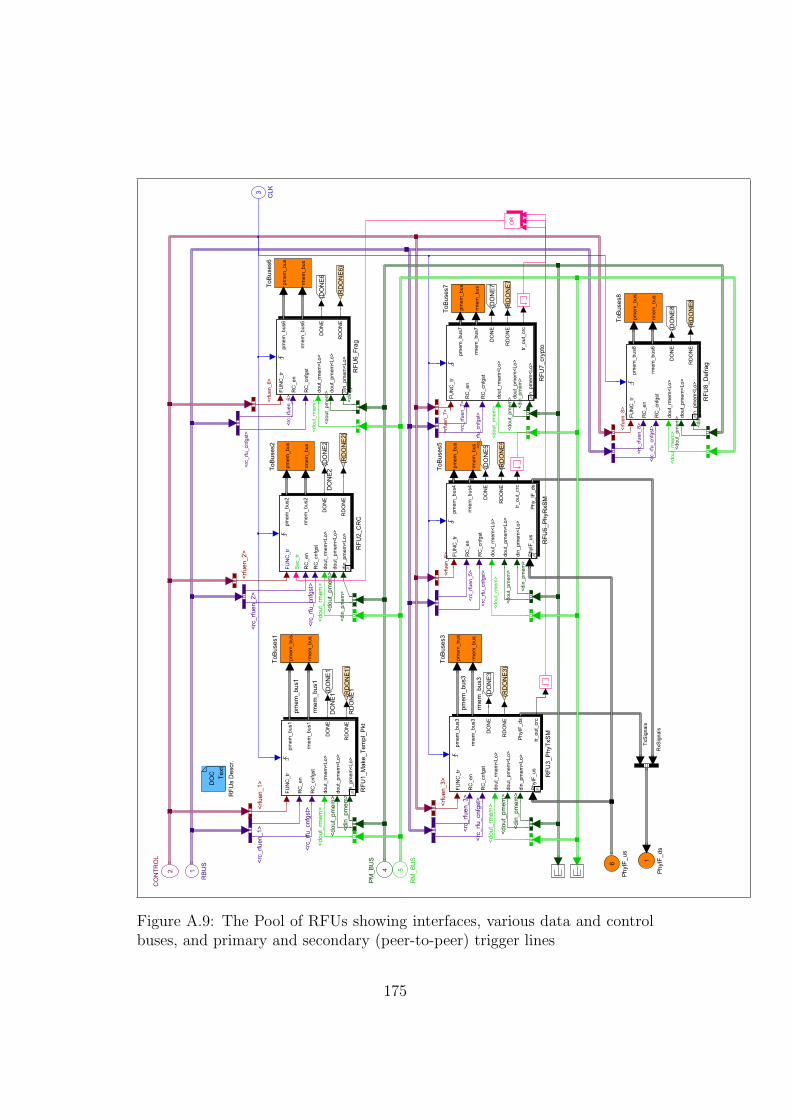
Phy
IF_d
s
1
{RD
ON
E8
{RD
ON
E7
{RD
ON
E6}
{RD
ON
E2}
{RD
ON
E5
{RD
ON
E1}
{RD
ON
E3}
ToB
uses
8
pmem
_bus
rmem
_bus
ToB
uses
7
pmem
_bus
rmem
_bus
ToB
uses
6
pmem
_bus
rmem
_bus
ToB
uses
5
pmem
_bus
rmem
_bus
ToB
uses
3
pmem
_bus
rmem
_bus
ToB
uses
2
pmem
_bus
rmem
_bus
ToB
uses
1
pmem
_bus
rmem
_bus
RFU
s D
escr
.
DO
C Text
RFU
8_D
efra
g
FUN
C_t
r
RC
_en
RC
_cnf
gst
dout
_rm
em<L
o>
dout
_pm
em<L
o>
din_
pmem
<Lo>
pmem
_bus
8
rmem
_bus
6
DO
NE
RD
ON
E
RFU
7_cr
ypto
FUN
C_t
r
RC
_en
RC
_cnf
gst
dout
_rm
em<L
o>
dout
_pm
em<L
o>
din_
pmem
<Lo>
pmem
_bus
7
rmem
_bus
7
DO
NE
RD
ON
E
tr_ou
t_cr
c
RFU
6_Fr
ag
FUN
C_t
r
RC
_en
RC
_cnf
gst
dout
_rm
em<L
o>
dout
_pm
em<L
o>
din_
pmem
<Lo>
pmem
_bus
6
rmem
_bus
6
DO
NE
RD
ON
E
RFU
5_P
hyR
xSM
FUN
C_t
r
RC
_en
RC
_cnf
gst
dout
_rm
em<L
o>
dout
_pm
em<L
o>
din_
pmem
<Lo>
Phy
IF_u
s
pmem
_bus
4
rmem
_bus
4
DO
NE
RD
ON
E
tr_ou
t_cr
c
Phy
_IF_
ds
RFU
3_P
hyTx
SM
FUN
C_t
r
RC
_en
RC
_cnf
gst
dout
_rm
em<L
o>
dout
_pm
em<L
o>
din_
pmem
<Lo>
Phy
IF_u
s
pmem
_bus
3
rmem
_bus
3
DO
NE
RD
ON
E
Phy
IF_d
s
tr_ou
t_cr
c
RFU
2_C
RC
FUN
C_t
r
Sec
_tr
RC
_en
RC
_cnf
gst
dout
_rm
em<L
o>
dout
_pm
em<L
o>
din_
pmem
<Lo>
pmem
_bus
2
rmem
_bus
2
DO
NE
RD
ON
E
RFU
1_M
ake_
Tem
pl_P
kt
FUN
C_t
r
RC
_en
RC
_cnf
gst
dout
_rm
em<L
o>
dout
_pm
em<L
o>
din_
pmem
<Lo>
pmem
_bus
1
rmem
_bus
1
DO
NE
RD
ON
E
OR
{DO
NE
2{D
ON
E1
{DO
NE
8{DO
NE
7
{DO
NE
6
{DO
NE
5{D
ON
E3
Phy
IF_u
s
6
RM
_BU
S
5
PM
_BU
S
4
CLK3
CO
NTR
OL
2
RB
US
1
<dou
t_rm
em>
<dou
t_pm
em>
<din
_pm
em>
<rc_
rfu_c
nfgs
t>
<rc_
rfuen
_8>
<rfu
en_8
>
RxS
igna
ls
TxS
igna
ls
<rc_
rfu_c
nfgs
t>
<rc_
rfuen
_2>
<rc_
rfu_c
nfgs
t>
<rc_
rfuen
_1>
<rfu
en_2
>
<din
_pm
em>
RD
ON
E1
<rfu
en_1
>
DO
NE
2D
ON
E1
rmem
_bus
1<d
out_
rmem
><d
out_
rmem
>
pmem
_bus
1
<rfu
en_3
>
<rc_
rfu_c
nfgs
t>
<rc_
rfuen
_3>
<dou
t_rm
em>
<din
_pm
em>
<dou
t_pm
em>
<dou
t_pm
em>
<dou
t_pm
em>
pmem
_bus
3
rmem
_bus
3
<rfu
en_5
>
<rc_
rfuen
_5>
<rc_
rfu_c
nfgs
t>
<dou
t_rm
em>
<dou
t_pm
em>
<din
_pm
em>
<din
_pm
em>
<dou
t_pm
em>
<dou
t_rm
em><r
fuen
_6>
<rc_
rfuen
_6>
<rc_
rfu_c
nfgs
t> <rfu
en_7
>
<rc_
rfuen
_7>
<rc_
rfu_c
nfgs
t>
<din
_pm
em>
<dou
t_pm
em>
<dou
t_rm
em>
<din
_pm
em>
Figure A.9: The Pool of RFUs showing interfaces, various data and controlbuses, and primary and secondary (peer-to-peer) trigger lines
175

(state==1) => encryption(state==2) => decryption
Not needed but just to keepa uniform interface.
If RC_en, then load new value,otherwise remain in thesame context
Since This RFU reconfigures byswitching context only, the RDONEis sent automatically (after some ticks)
Source Pointer
Size
Header Size
Destination Pointer
Key
tr_out_crc5
RDONE4
DONE3
rmem_bus72
pmem_bus71
on
Display
state_reg
state_reg
state_reg
ARG5
ARG4
ARG1
ARG3
rfu_id
state_reg
ARG2
MYADDRESS
0
CRYPT
dout_pmem
state_in
func_tr
din_pmem_r
DONE
addr
din_mem
wr_en_mem
tr_out_crc
Trigger
din_pmem6<Lo>
dout_pmem5<Lo>
dout_rmem4<Lo>
RC_cnfgst3
RC_en2
FUNC_tr1
addr_rmem
wr_en_pmem
din_pmem
addr_pmem
Figure A.10: Inside the subsystem that is the RFU for encryption and decryp-tion. Note the stateflow block containing encryption logic, the context-switchlogic, the state registers, and the interface signals.
176

If (s
tate
_in=
=1) -
-> W
ifi E
ncry
ptio
nA
RG
1 =
Poi
nter
to p
lain
-text
PD
UA
RG
2 =
Siz
e of
PD
U p
acke
t inc
hea
der
AR
G3
= S
ize
of P
DU
Hea
der (
not t
o en
cryp
t)A
RG
4 =
Des
tinat
ion
Poi
nter
(for
cip
herte
xt)
AR
G5
= E
ncry
ptio
n K
ey (f
or P
RN
G)
AR
G6
= R
FU_I
D o
f Sla
ve C
RC
RFU
for B
us G
rant
??
eM
y
= R
C4_
PR
NG
(Key
, Siz
e)B
RE
AK
DO
NE
= 0
;A
RG
S e
M
y =
Enc
rypt
_wor
d(pt
ext_
wor
d, p
rng_
wor
d)
eM
y
= D
ecry
pt_w
ord(
ctex
t_w
ord,
prn
g_w
ord)
If (s
tate
_in=
=2) -
-> W
ifi D
ecry
ptio
nA
RG
1 =
Poi
nter
to c
iphe
r-te
xt P
DU
AR
G2
= S
ize
of P
DU
pac
ket i
nc h
eade
rA
RG
3 =
Siz
e of
PD
U H
eade
r (no
t to
decr
ypt)
AR
G4
= D
estin
atio
n P
oint
er (f
or p
lain
text
)A
RG
5 =
Dec
rypt
ion
Key
(for
PR
NG
)A
RG
6 =
RFU
_ID
of S
lave
CR
C R
FU fo
r Bus
Gra
nt ?
?
WA
IT/*
for f
unc_
tr to
be
enab
led
agai
n*/
AR
GS
_2_C
RC
_RFU
INIT
_FU
NC
Rea
d_W
rite_
Dis
able
_H
Rea
d_E
ncry
pt_W
rite_
Dis
able
_D
RE
AD
_WR
ITE
_HE
AD
ER
Rea
d_D
ecry
pt_W
rite_
Dis
able
_D
RE
AD
_EN
CR
YP
T_W
RIT
E_D
ATA
_DO
NE
DIA
BLE
_AN
D_W
AIT
_FO
R_R
ES
PO
NS
E
BU
S_G
RA
NT_
OV
ER
RID
E_2
_CR
C_R
FU
RE
AD
_CR
C_R
ETU
RN
DIA
BLE
_AN
D_W
AIT
_FO
R_D
ON
E
WA
IT4b
usW
RIT
E_E
NC
RY
PTE
D_I
CV
WA
IT5
[func
_tr =
= 1]
{dbg
_rfu
7=1}
{dbg
_rfu
7=0}
[func
_tr =
= 0]
[func
_tr =
= 1]
{pnt
r_pt
ext =
AR
G3
%re
lativ
e to
AR
G1;
hea
der s
kipp
edpn
tr_ct
ext =
0 %
rela
tive
to A
RG
4en
c_st
ring
= R
C4_
PR
NG
(AR
G5,
AR
G2
- AR
G3
);}
{w_c
ount
= A
RG
3i =
0}
[i<w
_cou
nt]
1{i+
+}
2
/*en
cryp
ting*
/[(st
ate_
in==
1) ||
(sta
te_i
n==3
) || (
stat
e_in
==5)
]1
[i<w
_cou
nt]
1
2{w
_cou
nt =
AR
G2
- AR
G3
i = 0
}{i+
+}/*
assu
med
dec
sta
te --
> 2,
4,6
*/
2
{i++}
/* A
sser
t the
spe
cial
add
ress
that
will
ove
r_rid
e bu
s gr
ant
and
also
ase
rt on
dat
a bu
s th
e id
of s
lave
RFU
Als
o tri
gger
sla
ce R
FU to
indi
cate
bus
is a
vaila
ble*
/{ ad
dr =
BU
S_G
RN
T_O
RID
Edi
n_m
em =
2w
r_en
_mem
= 1
tr_ou
t_cr
c =
1}
{wr_
en_m
em =
0tr_
out_
crc
= 0}
/* If
dec
rypt
ing
*/[(f
unc_
tr ==
1) &
& (
(sta
te_i
n==2
) || (
stat
e_in
==4)
|| (s
tate
_in=
=6) )
]{IC
V_c
text
= d
in_p
mem
_r%
read
ICV
from
CR
C}
2/*
If e
ncry
ptin
g */
[(fun
c_tr
== 1
) &&
( (s
tate
_in=
=1) |
| (st
ate_
in==
3) ||
(sta
te_i
n==5
))]
{ICV
_cte
xt =
Enc
rypt
_wor
d(di
n_pm
em_r
, enc
_stri
ng[i]
)%
read
ICV
from
CR
C, a
nd e
ncry
pt}
1
[func
_tr =
= 0]
{wr_
en_m
em =
0}
/*sl
ave
RFU
indi
cate
s do
ne b
y w
ritin
g to
the
Mas
ter R
FU's
add
ress
i.e.
trig
gerin
g it*
/[fu
nc_t
r ==
1]/*
encr
yptin
g*/
[(sta
te_i
n==1
) || (
stat
e_in
==3)
|| (s
tate
_in=
=5)]
1/*
Hav
e to
wai
t som
e tic
ks s
o th
at b
us c
ontro
l ha
s be
en re
turn
ed b
y th
e C
RC
-RFU
*/af
ter(
3,tic
k){d
in_m
em =
ICV
_cte
xtad
dr =
(AR
G4
+ pn
tr_ct
ext)
+ A
RG
3 +
i %
writ
e ci
pher
-ICV
on
the
next
ava
ilabl
e lo
catio
nw
r_en
_mem
= 1
}/*
decr
yptin
g*/
2
{wr_
en_m
em =
0}
/*IC
V-E
rror
*/2
/*co
rrec
t IC
V, s
end
DO
NE
*/[IC
V_r
ecei
ved=
=IC
V_c
text
]1
{DO
NE
= rf
u_id
}
Figure A.11: The stateflow chart of the encryption / decryption RFU. Re-ceives arguments, writes header, encrypts or decrypts, and calculates orchecks redundancy value using slave RFU.
177
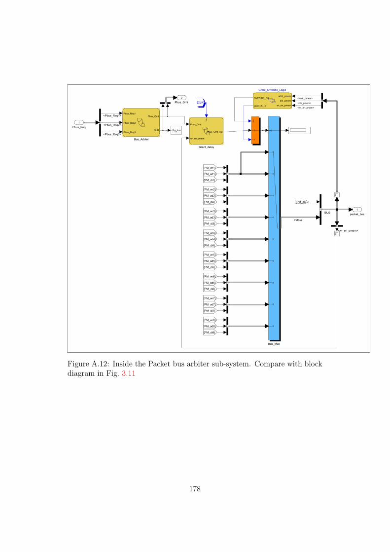
Pbus_Grnt2
packet_bus1
Grant_delay
Pbus_Grnt
wr_en_pmem
Pbus_Grnt_out
Grant_Override_Logic
addr_pmem
din_pmem
wr_en_pmem
OVERIDE_OK
grant_rfu_id
{PM_ad4}
{PM_wr4}
{PM_di2}
{PM_ad2}
{PM_do}
{PM_wr2}
{PM_di1}
{PM_ad8}
{PM_wr8}
{PM_di8}
{PM_ad7}
{PM_wr7}
{PM_di7}
{PM_ad1}
{PM_ad6}
{PM_wr6}
{PM_di6}
{PM_ad5}
{PM_wr5}
{PM_di5}
{PM_di3}
{PM_ad3}
{PM_wr3}
{PM_di4}
{PM_wr1}
{CLK}
dbg_bus
Bus_Mux
Bus_Arbiter
Pbus_Req1
Pbus_Req2
Pbus_Req3
Pbus_Grnt
GrIDPbus_Req
1
BUS
PMbus
<Pbus_Req1>
<Pbus_Req2>
<Pbus_Req3>
<wr_en_pmem>
<addr_pmem>
<din_pmem>
<wr_en_pmem>
Figure A.12: Inside the Packet bus arbiter sub-system. Compare with blockdiagram in Fig. 3.11
178
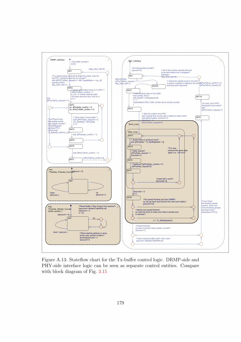
PHY_Interface 1
INIT
INIT25
INIT2
INIT10
INIT3
INIT9
Word_Loop
Byte_Loop
INIT4
INIT5
INIT6
INIT7
INIT8
DRMP_Interface 2
INIT
INIT2
INIT3du: dPhyData_confirm = 0;du: dPhyTxStart_confirm = 0;
INIT4
INIT5
INIT6
INIT7
PFC/*Packets_Finished_Counter*/
3
INIT
PSC/*Packets_Started_Counter(Write counter) */
4
INIT
/*init read packet counter*/{rpcount=0} /*init to the number packets that are
to be sent before sim is stopped*/{simstop--dbg_txbuf_piA=0}
/* whenever packet count is not zeroit means a packet is waiting to be sent*/dclk [rpcount!=wpcount]
[pPhyTxEnd_confirm==1]{pPhyTxEnd_request=0}
after(20,dclk){pPhyTxStart_request = 1dbg_txbuf_piA=1}
/*read starting index in the bufferfrom pindex array*/dclk {pstarti = pindex[rpcount]i = 1%send(down,PSC) %Do not dec since circular counter} /*on pclk, ind to PHY
that packet has ended*/pclk{pPhyTxEnd_request=1}
/* Wait for confirm from PHYstart counter that counts upto 4 bytes for each word*/dclk [pPhyTxStart_confirm==1]{bcounter = 0pPhyTxStart_request=0}
/*count downthe finished packetcounter, since oneof the finished packetshas been sent*/{send(down,PFC)}
/*Packet finishedcircular increment read_packet_counter*/{rpcount++}
2
2
/*Have reached buffer limit?; then rese*/[rpcount==ModeATxBufPktLmt]
1
{bcounter = 0i++}
2
/*No packet finished yet (from DRMP)so can go back and transmit the next word safely*/[pfcount==0]
1/*atleast one packet finishedso read first word of index and check if packet sizeis reached*/
2
[ i < Tx_Buffer[pstarti] ]1
/*For now,transmit the same dataagain (i.e. i not inc)*/
/* Assert Data on protocol clock*/pclk {pPhyData = Tx_Buffer[pstarti + i]}
/*make request*/{pPhyData_request = 1bcounter++}
/*wait4conf*/[pPhyData_confirm==1]{pPhyData_request=0}
/*bytes left in word*/[bcounter<4]
1
/*init buffer counter*/{k=0}
{dbg_txbuf_diA=0}
/*if a packet being received & target thsi mdoe ,then letthe PHY_interface know by inc counter*/dclk [dPHYTxStart_request==1 && TargetMode == my_id]{send(up,PSC)dbg_txbuf_diA=1}
/* Send confirmation back to Tx-RFU */{dPhyTxStart_confirm = 1k_init = k %store starting index%to later save the size, and inc itk++}dclk
[dPhyTxEnd_request==1]
2
/*Let Phyint knowthat packet endedand update counter*/{TxEndRequestsend(up,PFC)%store sizeTx_Buffer[k_init]=k-k_init}
/* Store data in local buffer */dclk [dPHYData_request==1]{Tx_Buffer[k] = dPhyDatak++}
1
dclk {dPhyData_confirm = 1}
dclk {dPhyTxEnd_confirm = 1}
{dPhyTxEnd_confirm=0}
{pfcount = 0}
up{pfcount++}
1
down{pfcount--}
2
{wpcount = 0}
up1
/*Reset Buffer if Max Packet limit reached*/[wpcount==ModeATxBufPktLmt]{wpcount = 0k = 0}
1
down / wpcount--
2
2
/*Store starting address in arrayat the read_pointer location*/{pindex[wpcount] = kwpcount++}
Figure A.13: Stateflow chart for the Tx-buffer control logic. DRMP-side andPHY-side interface logic can be seen as separate control entities. Comparewith block diagram of Fig. 3.15
179
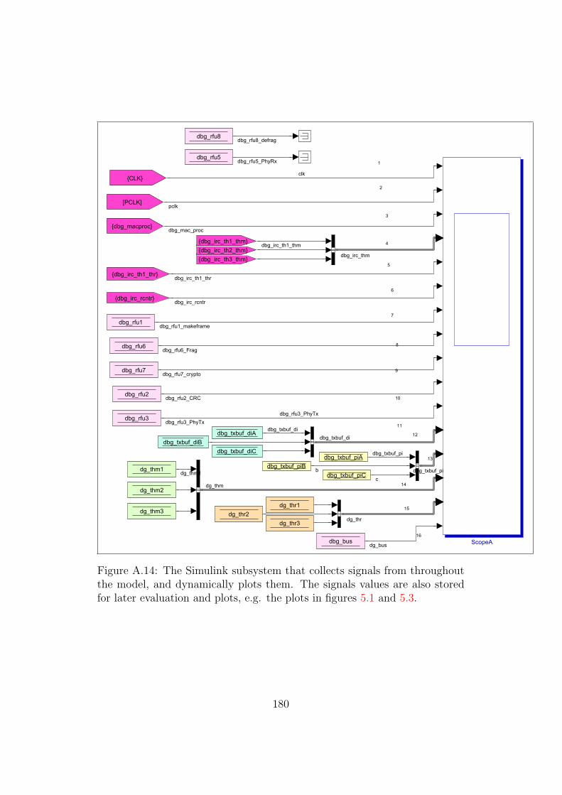
1
2
3
4
5
6
7
8
9
10
11
12
14
13
15
16ScopeA
{dbg_irc_th3_thm}{dbg_irc_th2_thm}
[PCLK]
{CLK}
{dbg_irc_rcntr}
{dbg_macproc}
{dbg_irc_th1_thr}
{dbg_irc_th1_thm}
dbg_txbuf_piA
dbg_txbuf_diA
dbg_rfu5
dbg_rfu8
dbg_rfu3
dbg_rfu2
dbg_rfu7
dbg_bus
dbg_rfu6
dg_thr3dg_thr2
dg_thr1dg_thm3
dg_thm2
dg_thm1dbg_txbuf_piC
dbg_txbuf_piB
dbg_txbuf_diBdbg_txbuf_diC
dbg_rfu1
dbg_mac_proc
dbg_irc_th1_thm
dbg_irc_th1_thr
dbg_irc_rcntr
clk
pclk
dbg_rfu1_makeframe
dbg_rfu3_PhyTxdbg_rfu3_PhyTx
dbg_rfu5_PhyRx
dbg_rfu7_crypto
dbg_rfu8_defrag
dbg_rfu2_CRC
dbg_rfu6_Frag
dbg_txbuf_di
dbg_txbuf_pi
dbg_irc_thm
dbg_txbuf_di
b
cdbg_txbuf_pidg_thm1
dg_thm
dg_thr
dg_bus
Figure A.14: The Simulink subsystem that collects signals from throughoutthe model, and dynamically plots them. The signals values are also storedfor later evaluation and plots, e.g. the plots in figures 5.1 and 5.3.
180
Appendix B
Detailed Comparison of Wifi,
WiMAX and UWB
In section 2.3.2, we took a brief comparative look at the features of the
three MAC protocols that have been investigated for this project, i.e. IEEE
Std. 802.11 (WiFi), IEEE Std. 802.16 (WiMAX) and IEEE Std. 802.15.3
(UWB). Here we look at this comparison in some detail in tabulated form.
This comparison played a crucial part in determining the design of the DRMP
architecture, the partition of tasks between software and hardware, and the
granularity and functionality of RFUs.
181

IEE
E 8
02.1
1 (
WiF
i)IE
EE
802.1
5.3
(U
WB
)IE
EE
802.1
6 (
WiM
AX
)
1D
ata
Rate
s1, 2, 5.5
and 1
1 M
bps
20 M
bps (
802.1
5.3
)U
pto
72 M
bps (
share
d),
low
er
for
mobile
WiM
AX
2F
ram
e B
od
y (
MP
DU
)30 (
header)
+ 4
(F
CS
) +
0-2
312
(Paylo
ad)
= 2
346 b
yte
s M
AX
2048 b
yte
s (
exclu
din
g M
AC
headerm
PH
Y p
ream
ble
or
header)
Variable
Length
.
Only
header
is m
andato
ry.
Paylo
ad/C
RC
optional.
3H
EC
16-b
it C
RC
The 1
6-b
it H
eader
Check S
equence
is the s
am
e a
s that fo
r 802.1
1
8-b
it H
CS
(H
eader
Check S
equence)
(involv
es m
odule
-2 d
ivis
ion a
nd
multip
lication)
4F
ram
e C
heck S
eq
uen
ce
(CR
C)
32-b
it C
RC
32-b
it C
RC
32-b
it C
RC
(optional)
5A
dd
resses
48-b
it 8
02 fam
ilt M
AC
addre
ss
1-o
cte
t D
EV
ID u
sed (
is a
ssig
ned a
t
join
ing the P
iconet)
inste
ad o
f th
e
MA
C a
ddre
ss
48-b
it 8
02 fam
ilt M
AC
addre
ss b
ut
Connection ID
is the p
rim
ary
access
mechanis
m
6F
rag
men
tati
on
Yes -
based o
n a
fra
gm
enta
tion
thre
shold
.
Tim
eout as w
ell.
Yes. B
ased o
n thre
shold
.Y
es. (h
as a
sub-h
eader
to d
eal w
ith it)
7P
ackag
ing
No
No.
Yes. (h
as a
sub-h
eader
to d
eal w
ith it)
8A
ccess M
eth
od
s1. C
onte
ntion A
ccess in D
CF
mode
2. C
onte
ntion-f
ree p
oll-
based a
ccess in
the P
CF
modeq
Superf
ram
e h
as tw
o d
istinct periods:
1. C
onte
nta
ion-a
ccess p
eriod
(CS
MA
)
2. C
ontion-f
ree p
eriod (
TD
MA
)
1. consta
nt bit-r
ate
(U
GS
)
2. R
eal-tim
e p
olli
ng w
ith v
ariable
bit
rate
3. N
on-R
-T p
olli
ng w
ith v
ar
bit r
ate
4. B
est effort
(conte
ntion a
ccess)
9T
DM
/ T
DM
AN
o. U
ses C
onte
ntion a
ccess a
nd p
olli
ng
Yes. T
DM
A in the C
onte
ntion-f
ree
period o
f th
e s
uperf
ram
e
Yes. E
ssentially
TD
M s
yste
m:
- T
DM
A for
uplin
k (
because m
ultip
le
transm
itte
rs)
/
- T
DM
A for
dow
nlin
k.
10
Co
nte
nti
on
Access a
nd
Exp
on
en
tial B
acko
ff
CS
MA
/CA
is the a
ccess m
eth
od in the
dom
inant m
ode o
f opera
tion (
DC
F).
Uses e
xponential backoff a
lgo.
CS
MA
/Exponential B
ackoff u
sed in
the C
onte
ntion-A
ccess p
eriod o
f th
e
superf
ram
e.
Exponential B
ackoff (
truncate
d)
used
for
BW
request / In
itia
l ra
nge-r
equest
slo
t
1
182

IEE
E 8
02
.11
(W
iFi)
IEE
E 8
02
.15
.3 (
UW
B)
IEE
E 8
02
.16
(W
iMA
X)
11
Po
llin
g
Po
llin
g is a
do
pte
d in
th
e P
CF
mo
de
-
no
n-d
om
ina
nt
an
d m
ostly n
ot
imp
lem
en
ted
No
. T
he
tw
o m
od
es a
re C
SM
A a
nd
TD
MA
Ye
s.
Bo
th R
-T a
nd
no
n R
-T p
olli
ng
12
Fra
me
Ty
pe
s/F
orm
ats
Da
ta
Co
ntr
ol
Ma
na
ge
me
nt
with
su
bty
pe
s
Co
mm
an
d
Da
ta
Be
aco
n
AC
Ks
Ha
s t
wo
he
ad
er
form
ats
:
1
. G
en
eric h
ea
de
r
2
. B
W r
eq
ue
st
he
ad
er
13
He
ad
er
co
nte
nts
/
Su
bh
ea
de
rs
Th
e f
ram
e h
ea
de
r h
as:
F
ram
e C
on
tro
l,
D
ura
tio
n/I
D,
A
dd
resse
s a
nd
S
eq
ue
nce
Co
ntr
ol
2-b
yte
fra
me
co
ntr
ol te
lls if:
mo
re f
rag
s,
fro
m a
nd
to
ad
dre
sse
s p
rese
nt,
retr
y s
tat,
wa
itin
g d
ata
sta
t,
en
cry
pte
d o
r n
ot
Th
e h
ea
de
r h
as in
fo a
bo
ut
ad
dre
sse
s,
fra
gm
en
tatio
n c
on
tro
l,
an
d h
as a
fra
me
co
ntr
ol.
Fra
me
co
ntr
ol te
lls if
mo
re d
ata
wa
itin
g,
if t
his
is r
etr
y,
the
AC
K p
olic
y,
am
on
g o
the
r th
ing
s
Ha
s (
op
tio
na
l) s
ub
he
ad
ers
:
1.
Gra
nt
ma
na
ge
me
nt
2.
Fra
gm
en
tatio
n
3.
Pa
cka
gin
g
4.
Me
sh
su
b-h
ea
de
r
he
ad
er
fie
lds in
dic
ate
wh
ich
of
the
se
su
b-h
ea
de
rs is p
rese
nt.
He
ad
er
als
o in
dic
ate
s if
the
pa
ylo
ad
is
AR
Q f
ee
db
ack.
Th
e F
ram
e's
'Co
ntr
ol'
ha
s D
L-M
AP
an
d U
L-M
AP
in
form
atio
n
14
Su
pe
rfra
me
s
In P
CF
mo
de
, a
'su
pe
rfra
me
' sim
ilar
to
the
ca
se
fo
r U
WB
. H
as a
CF
P (
po
llin
g)
an
d t
he
n a
CA
P (
CS
MA
/CA
).
No
te d
ifff
ere
nce
fro
m U
WB
. In
UW
B,
CF
P is T
DM
A,
he
re it
is p
olli
ng
Ha
s a
'su
pe
rfra
me
' th
at
co
nsis
ts o
f:
1.
Ne
two
rk b
ea
co
n in
terv
al
2.
Co
nte
ntio
n A
cce
ss P
erio
d(C
AP
)
3.
Co
nte
ntio
n F
ree
Pe
rio
d(C
FP
)
No
.
15
Ad
-Ho
c n
etw
ork
s
Ye
s (
op
tio
na
l).
No
AP
re
qu
ire
d.
Ju
st
two
sta
tio
ns m
ay
co
mm
un
ica
te
Als
o c
alle
d I
BS
S.
Ye
s.
Esse
ntia
lly a
n a
d-h
oc n
etw
ork
with
on
e d
evic
e b
eco
min
g t
he
co
-
ord
ina
tor
(PN
C).
Th
e P
NC
ma
y
ch
an
ge
dyn
am
ica
lly in
a p
ico
ne
t
op
era
tio
n.
All
de
vic
es n
ee
d n
ot
ha
ve
PN
C c
ap
ab
ilitie
s.
No
.
No
te t
ha
t M
esh
op
era
tio
n d
oe
s a
llow
pe
er
2 p
ee
r b
ut
tha
t a
lso
in
vo
lve
s B
S
invo
lve
me
nt
to s
etu
p.
2
183

IEE
E 8
02
.11
(W
iFi)
IEE
E 8
02
.15
.3 (
UW
B)
IEE
E 8
02
.16
(W
iMA
X)
16
AR
QN
o.
No
Yes. Is
handle
d in the M
AC
layer
(is
possib
le in the P
HY
as w
ell)
.
Optional fo
r im
ple
menta
tion
17
AC
Ks
Yes. S
ent in
DC
F m
odes. A
bsence
(when A
CK
expecte
d)
indic
ate
s
colli
ssio
n.
All
fram
es d
o n
ot re
q A
CK
. E
.g.
bro
adcast fr
am
es
Yes.
Thre
e types:
Im
media
te
D
ela
yed (
Multip
le A
CK
s in a
sin
gle
MP
DU
)
Im
plie
d (
or
no A
CK
)
Used in a
n o
ptional A
RQ
schem
e (
H-
AR
Q)
and in r
esponse to s
om
e
managem
ent m
essages (
DS
x).
But appare
ntly n
ot on a
data
fra
me-b
y-
fram
e b
asis
.
18
Pig
gyb
ackin
g
Yes.
In P
CF
mode, C
F-A
CK
s c
an b
e
pig
gybacked o
n s
uccessic
e d
ata
fra
mes.
Appare
ntly n
ot. T
he D
ela
yed A
CK
may b
e c
onsid
ere
d s
imila
r to
pig
gybackin
g b
ut is
diffe
rent because
the A
CK
s a
re n
ot sent on a
data
MP
DU
, but gro
uped togeth
er
in a
sin
gle
dedic
ate
d M
PD
U.
Yes.
AR
Q feedbacks c
an b
e 'p
iggybacked'
on a
n e
xis
ting c
onnection (
in a
dditio
n
to b
ein
g s
ent separa
tely
on a
n
appro
priate
managem
ent connection)
19
Inte
r-F
ram
e S
paces
IFS
used to a
ssig
n p
rioro
ties. F
our
IFS
's
defined.
Yes a
nd v
ery
sim
ilar
to W
ifi. F
our
IFS
's d
efined h
ere
as w
ell.
Appare
ntly n
ot.
Has a
Colli
sio
n a
ccess m
echanis
m
but th
at is
essentially
for
BW
request
so IF
S not re
levant.
20
MA
C S
yn
ch
ron
izati
on
Thro
ugh b
eacon fra
mes.
Synch. to
a c
om
mon c
lock (
TS
F)
announced b
y b
eacon. A
ll S
TA
's to k
eep
a local copy o
f T
SF
.
All
DE
Vs s
ynch to the P
NC
clo
ck.
Beacon s
ent at th
e b
eggin
ing o
f every
superf
ram
e.
MA
C s
ynch. built
on top o
f P
HY
synch
pro
cess.
MA
C o
f S
S is in d
ow
nlo
ad s
ynch. as
long a
s it re
ceiv
es D
L-M
AP
.
Uplin
k is e
sta
blis
hed follo
win
g the
dow
nlin
k s
ynch.
3
184

IEE
E 8
02.1
1 (
WiF
i)IE
EE
80
2.1
5.3
(U
WB
)IE
EE
80
2.1
6 (
WiM
AX
)
21
Qo
S
In D
CF
mo
de
, so
me
so
rt o
f p
rio
rity
pro
vid
ed
by I
FS
's
- In
PC
F m
od
e,
sta
tio
ns a
re p
olle
d a
nd
be
tte
r Q
oS
th
an
DC
F t
ho
ug
h n
ot
en
ou
gh
for
ma
ny c
ase
s
- 8
02
.11
E e
nh
an
ce
me
nt
in t
he
MA
C
allo
ws f
or
be
tte
r Q
oS
Ye
s.
Un
like
80
2.1
1 Q
oS
is b
uilt
-in
.
- T
he
PN
C m
an
ag
es t
he
Qo
S
- G
oo
d Q
oS
gu
ara
nte
ed
be
ca
use
of
TD
MA
me
ch
an
ism
.
- P
NC
div
ide
s C
TA
's a
mo
ng
DE
V's
an
d t
he
DE
V is g
ura
nte
ed
no
t to
ha
ve
inte
rfe
ren
ce
du
rin
g t
ha
t C
TA
.
Co
mm
un
ica
tio
n is p
ee
r 2
pe
er.
Ye
s.
Qo
S is e
sse
ntia
l fa
cto
r o
f
WiM
AX
. A
va
ilab
le b
eca
use
of
TD
MA
na
ture
.
Fo
ur
mo
de
s p
rovid
e Q
oS
fo
r d
iffe
ren
t
typ
e o
f d
ata
/ap
plic
atio
n.
Als
o c
on
ce
pt
of
se
rvic
e f
low
s.
Ea
ch
se
rvic
e f
low
asso
cia
ted
with
a
pa
rtic
ula
r Q
oS
.
22
Co
nn
ec
tio
n-o
rie
nte
d
No
. D
om
ina
nt
mo
de
of
op
era
tio
n is
co
nn
ectio
n-le
ss.
Ma
y b
e c
on
sid
ere
d c
on
ne
ctio
n-o
rie
nte
d
in P
CF
mo
de
.
No
.
Ye
s.
Str
on
gly
co
nn
ectio
n-o
rie
nte
d
me
ch
an
ism
eve
n t
ho
ug
h a
pa
cke
t-
ba
se
d s
yste
m.
Ea
ch
sta
tio
n
asso
cia
ted
with
a n
um
be
r o
f
co
nn
ectio
n I
Ds.
CID
s a
re t
he
prim
ary
acce
s m
ech
an
ism
an
d a
re a
sso
cia
ted
with
a a
pa
rtic
ula
r Q
os.
23
Po
we
r M
od
es
Ye
s.
Active
mo
de
an
d P
ow
er-
Sa
ve
mo
de
.
In P
S p
acke
ts f
or
a S
TA
are
bu
ffe
red
at
the
AP
.
Ye
s.
Ha
s a
n A
CT
IVE
an
d a
HIB
ER
NA
TE
mo
de
No
lo
w-p
ow
er
mo
de
s s
imila
r to
Wifi/U
WB
.
Ho
we
ve
r, in
itia
l a
nd
dyn
am
ic r
an
gin
g
op
era
tio
ns s
et
the
op
tim
al tr
an
sm
it
po
we
r.
24
Sc
an
nin
gP
assiv
e a
nd
active
sca
nn
ing
.
Pro
be
s a
re s
en
t fo
r a
ctive
sca
nn
ing
Ye
s.
Pa
ssiv
e s
ca
nn
ing
on
ly t
o d
ete
ct
an
active
pic
on
et.
Se
em
s t
o d
o o
nly
pa
ssiv
e s
ca
nn
ing
by
wa
itin
g f
or
sp
ecific
me
ssa
ge
s.
25
Au
the
nti
ca
tio
n
Op
en
-syste
m a
nd
sh
are
d-k
ey
au
the
ntica
tio
n.
Th
e la
tte
r re
qu
rie
d W
EP
to b
e im
ple
me
nte
d.
Au
the
nctio
n is m
utu
al a
nd
ba
se
d o
n
pu
blic
-ke
y c
ryp
tog
rap
hy
Ba
se
d o
n P
KM
(P
riva
cy K
ey
Ma
na
ge
me
nt)
- a
cco
mo
da
tes A
ES
.
PK
M m
essa
ge
s u
se
HM
AP
Fo
r a
uth
en
tica
tio
n,
pu
blic
RS
A k
ey is
co
nta
ine
d in
X.5
09
dig
ita
l ce
rtific
ate
4
185
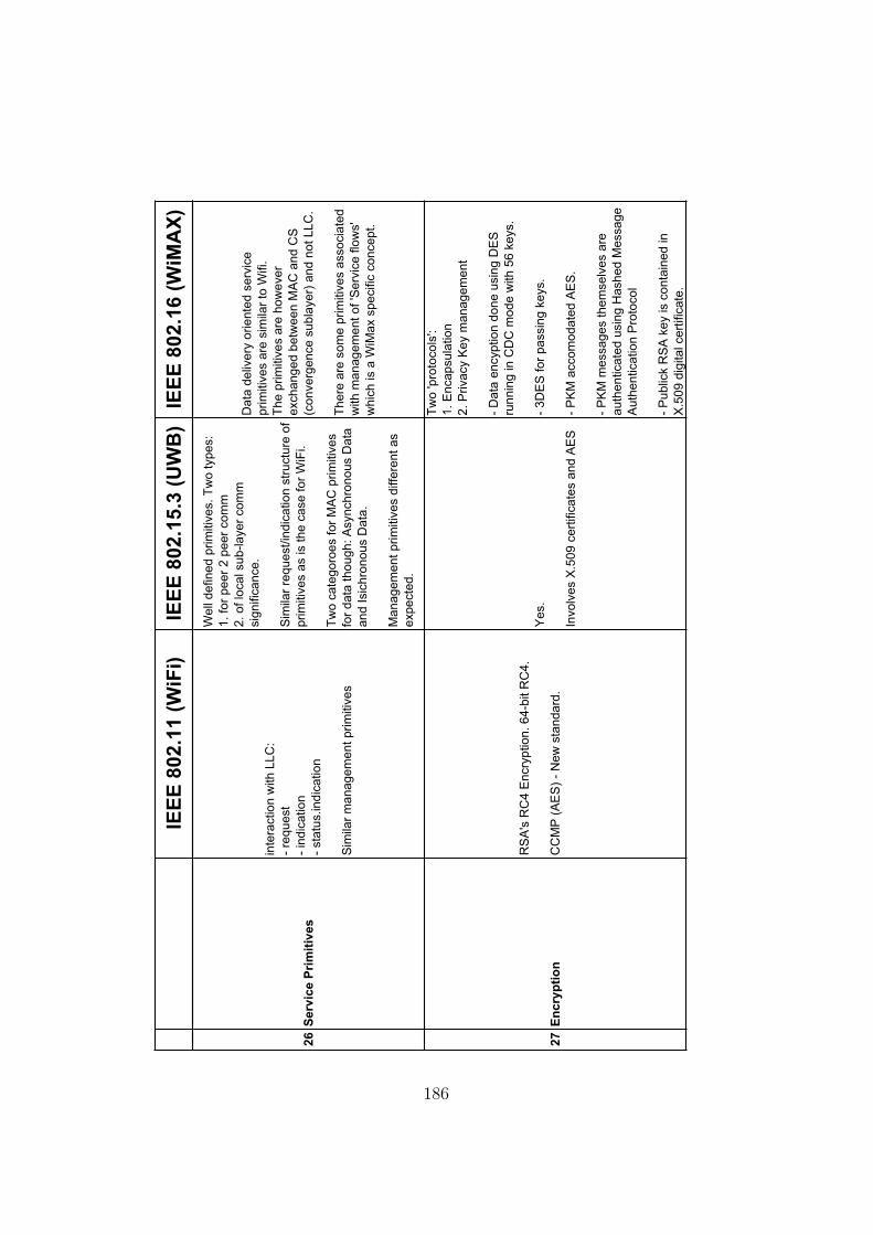
IEE
E 8
02.1
1 (
WiF
i)IE
EE
802.1
5.3
(U
WB
)IE
EE
802.1
6 (
WiM
AX
)
26
Se
rvic
e P
rim
itiv
es
inte
ractio
n w
ith
LL
C:
- re
qu
est
- in
dic
atio
n
- sta
tus.in
dic
atio
n
Sim
ilar
ma
na
ge
me
nt
prim
itiv
es
We
ll d
efin
ed
prim
itiv
es.
Tw
o t
yp
es:
1.
for
pe
er
2 p
ee
r co
mm
2.
of
loca
l su
b-la
ye
r co
mm
sig
nific
an
ce
.
Sim
ilar
req
ue
st/
ind
ica
tio
n s
tru
ctu
re o
f
prim
itiv
es a
s is t
he
ca
se
fo
r W
iFi.
Tw
o c
ate
go
roe
s f
or
MA
C p
rim
itiv
es
for
da
ta t
ho
ug
h:
Asyn
ch
ron
ou
s D
ata
an
d I
sic
hro
no
us D
ata
.
Ma
na
ge
me
nt
prim
itiv
es d
iffe
ren
t a
s
exp
ecte
d.
Da
ta d
eliv
ery
orie
nte
d s
erv
ice
prim
itiv
es a
re s
imila
r to
Wifi.
Th
e p
rim
itiv
es a
re h
ow
eve
r
exch
an
ge
d b
etw
ee
n M
AC
an
d C
S
(co
nve
rge
nce
su
bla
ye
r) a
nd
no
t L
LC
.
Th
ere
are
so
me
prim
itiv
es a
sso
cia
ted
with
ma
na
ge
me
nt
of
'Se
rvic
e f
low
s'
wh
ich
is a
WiM
ax s
pe
cific
co
nce
pt.
27
En
cry
pti
on
RS
A's
RC
4 E
ncry
ptio
n.
64
-bit R
C4
.
CC
MP
(A
ES
) -
Ne
w s
tan
da
rd.
Ye
s.
Invo
lve
s X
.50
9 c
ert
ific
ate
s a
nd
AE
S
Tw
o 'p
roto
co
ls':
1.
En
ca
psu
latio
n
2.
Priva
cy K
ey m
an
ag
em
en
t
- D
ata
en
cyp
tio
n d
on
e u
sin
g D
ES
run
nin
g in
CD
C m
od
e w
ith
56
ke
ys.
- 3
DE
S f
or
pa
ssin
g k
eys.
- P
KM
acco
mo
da
ted
AE
S.
- P
KM
me
ssa
ge
s t
he
mse
lve
s a
re
au
the
ntica
ted
usin
g H
ash
ed
Me
ssa
ge
Au
the
ntica
tio
n P
roto
co
l
- P
ub
lick R
SA
ke
y is c
on
tain
ed
in
X.5
09
dig
ita
l ce
rtific
ate
.
5
186
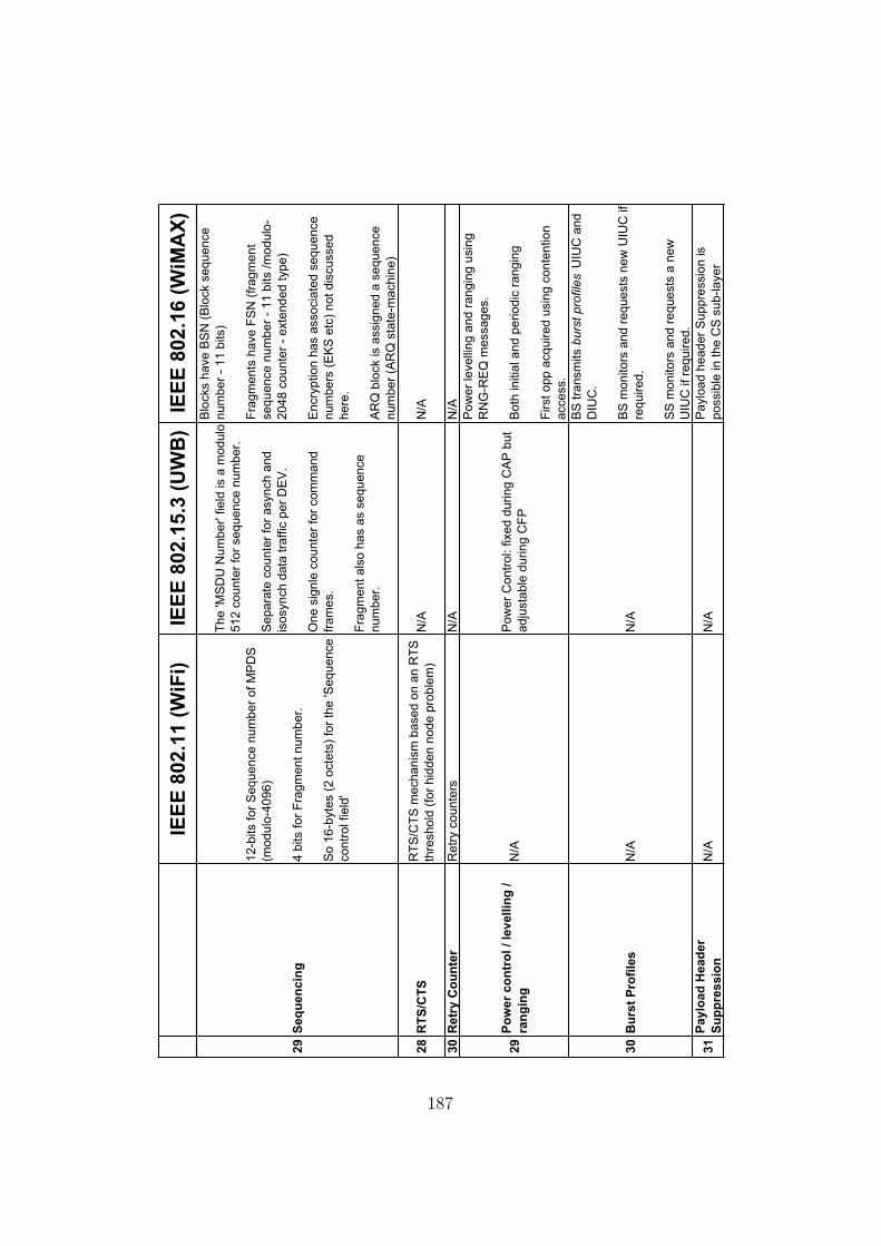
IEE
E 8
02.1
1 (
WiF
i)IE
EE
802.1
5.3
(U
WB
)IE
EE
802.1
6 (
WiM
AX
)
29
Se
qu
en
cin
g
12
-bits f
or
Se
qu
en
ce
nu
mb
er
of
MP
DS
(mo
du
lo-4
09
6)
4 b
its f
or
Fra
gm
en
t n
um
be
r.
So
16
-byte
s (
2 o
cte
ts)
for
the
'S
eq
ue
nce
co
ntr
ol fie
ld'
Th
e 'M
SD
U N
um
be
r' f
ield
is a
mo
du
lo
51
2 c
ou
nte
r fo
r se
qu
en
ce
nu
mb
er.
Se
pa
rate
co
un
ter
for
asyn
ch
an
d
iso
syn
ch
da
ta t
raff
ic p
er
DE
V.
On
e s
ign
le c
ou
nte
r fo
r co
mm
an
d
fra
me
s.
Fra
gm
en
t a
lso
ha
s a
s s
eq
ue
nce
nu
mb
er.
Blo
cks h
ave
BS
N (
Blo
ck s
eq
ue
nce
nu
mb
er
- 1
1 b
its)
Fra
gm
en
ts h
ave
FS
N (
fra
gm
en
t
se
qu
en
ce
nu
mb
er
- 1
1 b
its /
mo
du
lo-
20
48
co
un
ter
- e
xte
nd
ed
typ
e)
En
cry
ptio
n h
as a
sso
cia
ted
se
qu
en
ce
nu
mb
ers
(E
KS
etc
) n
ot
dis
cu
sse
d
he
re.
AR
Q b
lock is a
ssig
ne
d a
se
qu
en
ce
nu
mb
er
(AR
Q s
tate
-ma
ch
ine
)
28
RT
S/C
TS
RT
S/C
TS
me
ch
an
ism
ba
se
d o
n a
n R
TS
thre
sh
old
(fo
r h
idd
en
no
de
pro
ble
m)
N/A
N/A
30
Re
try
Co
un
ter
Re
try c
ou
nte
rsN
/AN
/A
29
Po
we
r c
on
tro
l /
lev
ell
ing
/
ran
gin
gN
/AP
ow
er
Co
ntr
ol: f
ixe
d d
urin
g C
AP
bu
t
ad
justa
ble
du
rin
g C
FP
Po
we
r le
ve
llin
g a
nd
ra
ng
ing
usin
g
RN
G-R
EQ
me
ssa
ge
s.
Bo
th in
itia
l a
nd
pe
rio
dic
ra
ng
ing
First
op
p a
cq
uire
d u
sin
g c
on
ten
tio
n
acce
ss.
30
Bu
rst
Pro
file
sN
/AN
/A
BS
tra
nsm
its b
urs
t p
rofile
s U
IUC
an
d
DIU
C.
BS
mo
nito
rs a
nd
re
qu
ests
ne
w U
IUC
if
req
uire
d.
SS
mo
nito
rs a
nd
re
qu
ests
a n
ew
UIU
C if
req
uire
d.
31
Pa
ylo
ad
He
ad
er
Su
pp
res
sio
nN
/AN
/AP
aylo
ad
he
ad
er
Su
pp
ressio
n is
po
ssib
le in
th
e C
S s
ub
-la
ye
r
6
187

IEE
E 8
02
.11
(W
iFi)
IEE
E 8
02
.15
.3 (
UW
B)
IEE
E 8
02
.16
(W
iMA
X)
32
Cla
ss
ifie
rN
/AN
/A
Cla
ssifie
r in
th
e s
erv
ice
-sp
ecific
co
nve
rga
nce
su
b-la
ye
r m
ap
s a
pa
cke
t
to a
pa
rtic
ula
r C
ID
33
Dy
na
mic
Ch
an
ne
l S
ele
cti
on
N/A
Dyn
am
ic C
ha
nn
el S
ele
ctio
n p
ossib
le
by t
he
PN
C
Dyn
am
ic r
an
gin
g/B
W r
eq
ue
st
is a
lon
g
the
sa
me
lin
es.
34
NA
V c
alc
ula
tio
n /
imp
lem
en
tati
on
Ye
s.
do
ne
usin
g t
he
in
co
min
g p
acke
t's
he
ad
er.
N/A
N/A
7
188
Bibliography
[1] Al-Hashimi, B. M. System-on-Chip: Next Generation Electronics.
Institution of Engineering and Technology, January 2006.
[2] Athanas, P. M., and Silverman, H. F. Processor reconfiguration
through instruction-set metamorphosis. Computer 26, 3 (Mar. 1993),
11–18.
[3] Bacchini, F., Rabaey, J., Cox, A., Lane, F., Lauwereins, R.,
Ramacher, U., and Witt, D. Wireless platforms: GOPS for cents
and Milliwatts. In Design Automation Conference, 2005. Proceedings.
42nd (June 13–17, 2005), pp. 351–352.
[4] Baschirotto, A., Castello, R., Campi, F., Cesura, G.,
Toma, M., Guerrieri, R., Lodi, R., Lavagno, L., and Malco-
vati, P. Baseband analog front-end and digital back-end for recon-
figurable multi-standard terminals. Circuits and Systems Magazine,
IEEE 6, 1 (Quarter 2006), 8–28.
[5] Becker, J., Pionteck, T., Habermann, C., and Glesner, M.
Design and implementation of a coarse-grained dynamically reconfig-
urable hardware architecture. In VLSI, 2001. Proceedings. IEEE Com-
puter Society Workshop on (Orlando, FL, Apr. 19–20, 2001), pp. 41–46.
[6] Benini, L., and Bertozzi, D. Network-on-chip architectures and
design methods. Computers and Digital Techniques, IEE Proceedings
- 152, 2 (Mar 2005), 261–272.
189

Bibliography
[7] Bondalapati, K., and Prasanna, V. K. Reconfigurable comput-
ing: Architectures, models and algorithms. Current Science 78 (2000),
828–837.
[8] Bondalapati, K., and Prasanna, V. K. Reconfigurable comput-
ing systems. Proceedings of the IEEE 90, 7 (July 2002), 1201–1217.
[9] Borkar, S. Getting gigascale chips: Challenges and opportunities in
continuing moore’s law. Queue 1, 7 (2003), 26–33.
[10] Brunelli, C., Garzia, F., Nurmi, J., Campi, F., and Picard,
D. Reconfigurable hardware: The holy grail of matching performance
with programming productivity. Field Programmable Logic and Ap-
plications, 2008. FPL 2008. International Conference on (Sept. 2008),
409–414.
[11] Cadence. Why care about power?, Feb. 2008. At http:
//www.cadence.com/rl/Resources/conference_papers/lptp_
01Overview.pdf. Last accessed on 5th April 2009.
[12] Carter, A. Using Dynamically Reconfigurable Hardware in Real-time
Communications systems – Literature survey. Tech. rep., University of
York, Real Time Systms Group, 2001.
[13] Chen, D., Cong, J., Fan, Y., and Zhang, Z. High-level power
estimation and low-power design space exploration for fpgas. Design
Automation Conference, 2007. ASP-DAC ’07. Asia and South Pacific.
[14] Chun, A., Tsui, E., Chen, I., Honary, H., and Lin, J. Ap-
plication of the Intel reconfigurable communications architecture to
802.11a, 3g and 4g standards. In Emerging Technologies: Frontiers of
Mobile and Wireless Communication, 2004. Proceedings of the IEEE
6th Circuits and Systems Symposium on (May 31–June 2, 2004), vol. 2,
pp. 659–662.
[15] Compton, K., and Hauck, S. Reconfigurable computing: a survey
of systems and software. ACM Comput. Surv. 34, 2 (2002), 171–210.
190
Bibliography
[16] CSR. Cambridge Silicon Radio official website. At http://www.csr.
com/.
[17] CSR. UniFi UF1050 product technical overview. Available at http://
www.csr.com/products/unifirange.htm. Last accessed on 5th April
2009.
[18] DeHon, A., and Wawrzynek, J. Reconfigurable computing: what,
why, and implications for design automation. In Design Automation
Conference, 1999. Proceedings. 36th (New Orleans, LA, June 21–25,
1999), pp. 610–615.
[19] Deshpande, S. D. Software implementation of IEEE 802.11b wireless
LAN standard. SDR 04 Technical Conference and Product Exposition
(2004).
[20] Elbirt, A. J., Yip, W., Chetwynd, B., and Paar, C. An FPGA-
based performance evaluation of the AES block cipher candidate algo-
rithm finalists. IEEE Transactions on Very Large Scale Integration
(VLSI) Systems 9, 4 (Aug. 2001), 545–557.
[21] Esquiagola, J., Ozari, G., Teruya, M., Strum, M., and Chau,
W. A dynamically reconfigurable bluetooth base band unit. Field
Programmable Logic and Applications, 2005. International Conference
on (Aug. 2005), 148–152.
[22] Ferrari, A., and Sangiovanni-Vincentelli, A. System design:
traditional concepts and new paradigms. Computer Design, 1999.
(ICCD ’99) International Conference on (1999), 2–12.
[23] Ferro, E., and Potorti, F. Bluetooth and wi-fi wireless protocols:
a survey and a comparison. Wireless Communications, IEEE 12, 1
(Feb. 2005), 12–26.
[24] Fourty, N., Val, T., Fraisse, P., and Mercier, J. J. Com-
parative analysis of new high data rate wireless communication tech-
nologies ”from Wi-fi to WiMAX”. In Autonomic and Autonomous
191

Bibliography
Systems and International Conference on Networking and Services,
2005. ICAS-ICNS 2005. Joint International Conference on (Oct. 23–
28, 2005), pp. 66–66.
[25] Fujistu Microelectronics. MB87M3550, the Fujitsu WiMAX
802.16-2004 SoC, product brief. Available at http://www.fujitsu.
com/downloads/MICRO/fma/pdf/wca_whitepaper_wimax.pdf. Last
accessed on 5th April 2009.
[26] Furber, S. ARM System-on-chip Architecture, second ed. Addison
Wesley, August 2000.
[27] Hamalainen, P., Hannikainen, M., Hamalainen, T., and
Snarinen, J. Hardware implementation of the improved WEP and
RC4 encryption algorithms for wireless terminals. The European Signal
Processing Conference (EUSIPCO’2000) (Sep 2000), 2289–2292.
[28] Haroud, M., Blazevic, L., and Biere, A. HW accelerated ultra
wide band MAC protocol using SDL and SystemC. Radio and Wireless
Conference, 2004 IEEE (Sept. 2004), 525–528.
[29] Hartenstein, R. Coarse grain reconfigurable architectures. Design
Automation Conference, 2001. Proceedings of the ASP-DAC 2001. Asia
and South Pacific (2001), 564–569.
[30] Hartenstein, R. A decade of reconfigurable computing: a visionary
retrospective. In Design, Automation and Test in Europe, 2001. Con-
ference and Exhibition 2001. Proceedings (Munich, Mar. 13–16, 2001),
pp. 642–649.
[31] Hauser, J. R., and Wawrzynek, J. Garp: a MIPS processor
with a reconfigurable coprocessor. In FPGAs for Custom Computing
Machines, 1997. Proceedings., The 5th Annual IEEE Symposium on
(Napa Valley, CA, Apr. 16–18, 1997), pp. 12–21.
[32] IEEE. IEEE standard for information technology - telecommunica-
tions and information exchange between systems - local and metropoli-
192
Bibliography
tan area networks - specific requirements part 15.3: wireless medium
access control (mac) and physical layer (phy) specifications for high
rate wireless personal area networks (wpans). IEEE Std 802.15.3-2003
(2003).
[33] IEEE. Information technology- telecommunications and information
exchange between systems- local and metropolitan area networks- spe-
cific requirements- part 11: Wireless lan medium access control (mac)
and physical layer (phy) specifications. ANSI/IEEE Std 802.11, 1999
Edition (R2003) (2003).
[34] IEEE. IEEE standard for local and metropolitan area networks part
16: Air interface for fixed broadband wireless access systems. IEEE
Std 802.16-2004 (Revision of IEEE Std 802.16-2001) (2004).
[35] IEEE. Draft standard for information technology-telecommunications
and information exchange between systems-local and metropolitan area
networks-specific requirements-part 11: Wireless lan medium access
control (mac) and physical layer (phy) specifications: Amendment 5:
Enhancements for higher throughput. IEEE Unapproved Draft Std
P802.11n/D5.0, May 2008 (2008).
[36] Iliopoulos, M., and Antonakopoulos, T. A methodology of im-
plementing medium access protocols using a general parameterized ar-
chitecture. In Rapid System Prototyping, 2000. RSP 2000. Proceedings.
11th International Workshop on (Paris, June 21–23, 2000), pp. 2–7.
[37] Iliopoulos, M., and Antonakopoulos, T. Optimised reconfig-
urable MAC processor architecture. In Electronics, Circuits and Sys-
tems, 2001. ICECS 2001. The 8th IEEE International Conference on
(Sept. 2–5, 2001), vol. 1, pp. 253–258.
[38] Iliopoulos, M., Maniatopoulos, A., and Antonakopoulos,
T. Design and implementation of a MAC controller for the IEEE802.11
wireless LAN. International Journal of Electronics 88, 3 (March 2001),
271–285.
193

Bibliography
[39] Intel. Intel ixp1200 network processor, datasheet. Avail-
able at http://download.intel.com/design/network/datashts/
27829810.pdf. Last accessed on 5th April 2009.
[40] Intel. The Intel WiMAX connection 2250, product brief. Available
at http://download.intel.com/network/connectivity/products/
wireless/IntelWiMAXConnection2250.pdf. Last accessed on 5th
April 2009.
[41] Intersil. Wireless LAN card WLANKITPR1-EVAL Datasheet.
[42] ITU. ICT market trends. Symposium on Telecommunications to
Commemorate the 10th Anniversary of the Fourth Protocol to the
GATS, Geneva, Switzerland (Feb. 2008). Available at http://www.
itu.int/ITU-D/ict/papers/2008/ITU_Gray_WTO.pdf. Last accessed
on 5th April 2009.
[43] ITU-T. ITU-T recommendation X.200; Data network and
open systems communications, Open systems interconnection–model
and notation. Available at http://www.itu.int/rec/T-REC-X.
200-199407-I/en. Last accessed on 5th April 2009.
[44] Keutzer, K., Malik, S., and Newton, A. R. From ASIC to
ASIP: the next design discontinuity. 2002. Proceedings. 2002 IEEE
International Conference on Computer Design: VLSI in Computers
and Processors (Sept. 16–18, 2002), 84–90.
[45] Kim, Y., Jung, H., Lee, H. H., and Cho, K. R. MAC implemen-
tation for IEEE 802.11 wireless LAN. ATM (ICATM 2001) and High
Speed Intelligent Internet Symposium, 2001. Joint 4th IEEE Interna-
tional Conference on (2001), 191–195.
[46] Kitsos, P., Kostopoulos, G., Sklavos, N., and Koufopavlou,
O. Hardware implementation of the RC4 stream cipher. In Circuits
and Systems, 2003. MWSCAS ’03. Proceedings of the 46th IEEE Inter-
national Midwest Symposium on (Dec. 27–30, 2003), vol. 3, pp. 1363–
1366.
194

Bibliography
[47] Knutson, C. Access isn’t always the killer application. Wireless
Systems Design (December 2004), 22–26. Also available at http:
//www.wsdmag.com/Articles/ArticleID/9420/9420.html. Last ac-
cessed on 5th April 2009.
[48] Koushanfar, F., Prabhu, V., Potkonjak, M., and Rabaey,
J. Processors for mobile applications. Computer Design, 2000. Pro-
ceedings. 2000 International Conference on (2000), 603–608.
[49] Lettieri, P., and Srivastava, M. B. Advances in wireless termi-
nals. IEEE [see also IEEE Wireless Communications] Personal Com-
munications 6, 1 (Feb. 1999), 6–19.
[50] Liu, Z., Arslan, T., Khawam, S., and Lindsay, I. A high perfor-
mance synthesisable unsymmetrical reconfigurable fabric for heteroge-
neous finite state machines. In Design Automation Conference, 2005.
Proceedings of the ASP-DAC 2005. Asia and South Pacific (Jan. 18–21,
2005), vol. 1, pp. 639–644.
[51] Logger, A., Upegui, A., Sanchez, E., and Gonzalez, I. Self-
reconfigurable pervasive platform for cryptographic application. Field
Programmable Logic and Applications, 2006. FPL ’06. International
Conference on (Aug. 2006), 1–4.
[52] Loraine, J. Integration is a must for future handsets. Wireless
Systems Design (December 2004), 22–26. Also available at http:
//www.wsdmag.com/Articles/Index.cfm?ArticleID=9421. Last ac-
cessed on 5th April 2009.
[53] Master, P. The next big leap in reconfigurable systems, a technology
vision whitepaper, 2001. Quicksilver Technology. Available at http://
www.qstech.com/pdfs/5-2_WP_NextBigLeap.pdf. Last accessed on
5th April 2009.
[54] Master, P. The next big leap in reconfigurable systems. Field-
Programmable Technology, 2002. (FPT). Proceedings. 2002 IEEE In-
ternational Conference on (Dec. 2002), 17–22.
195

Bibliography
[55] Mathworks. Mathworks product overview. At http://www.
mathworks.com/products/pfo/. Last accessed on 5th April 2009.
[56] Meyr, H. Why we need all these MIPS in future wireless communica-
tion systems-and how to design algorithms and architecture for these
systems. Signal Processing Systems, 2001 IEEE Workshop on (2001),
2.
[57] Mobile Dev & Design. SoC enables development of WiMAX-
compliant base stations and subscriber stations, Apr. 2005. Avail-
able at http://mobiledevdesign.com/hardware_news/radio_soc_
enables_development/. Last accessed on 5th April 2009.
[58] Morgan, P., and Taylor, R. ASIP Instruction Encoding for En-
ergy and Area Reduction. In Design Automation Conference, 2007.
DAC ‘07. 44th ACM/IEEE (San Diego, CA, USA, June 4–8, 2007),
pp. 797–800.
[59] Nabi, S. W., Wells, C. C., and Vanderbauwhede, W. A Dy-
namically Reconfigurable System-on-chip for Implementing Wireless
MACs. In Proceedings of the 2007 Ph.D Research in Microelectron-
ics and Electronics Conference (Bordeaux, France, July 2007), IEEE
Circuits and Systems Society, pp. 37–40.
[60] Nabi, S. W., Wells, C. C., and Vanderbauwhede, W. To-
wards a Dynamically Reconfigurable SoC for Wireless MACs in Con-
sumer Handheld Devices. In First Internationl Conference on Com-
puter, Control and Communication (Karachi, Pakistan, Nov. 12–13,
2007), pp. 182–191.
[61] Nabi, S. W., Wells, C. C., and Vanderbauwhede, W. A Dy-
namically Reconfigurable Hardware Co-Processor for a Multi-Standard
Wireless MAC Processor. In NASA/ESA Conference on Adaptive
Hardware and Systems (Noordwijk, The Netherlands, June 22–25,
2009). In Press.
196

Bibliography
[62] Ningyi, X., Dongjun, L., and Zucheng, Z. Protocol accelera-
tor design for IEEE 802.15.3 MAC implementation. Communications,
2004 and the 5th International Symposium on Multi-Dimensional Mo-
bile Communications Proceedings. The 2004 Joint Conference of the
10th Asia-Pacific Conference on 1 (Aug.-1 Sept. 2004), 189–192 vol.1.
[63] Ouellette, M., and Connors, D. Analysis of Hardware Accel-
eration in Reconfigurable Embedded Systems. In Parallel and Dis-
tributed Processing Symposium, 2005. Proceedings. 19th IEEE Inter-
national (Apr. 04–08, 2005).
[64] Paik, E. K., Kim, H., Heo, S. Y., Jin, J. S., Lee, S.-C., and
Lee, S. H. Development of mobile access point for vehicular wibro
networks. Advanced Communication Technology, 2008. ICACT 2008.
10th International Conference on 2 (Feb. 2008), 909–912.
[65] Panic, G., Dietterle, D., Stamenkovic, Z., and Tittelbach-
Helmrich, K. A system-on-chip implementation of the IEEE 802.11a
MAC layer. In Digital System Design, 2003. Proceedings. Euromicro
Symposium on (Sept. 1–6, 2003), pp. 319–324.
[66] picoChip. PC102 Product Brief, Mar. 2004. Available at http://www.
picochip.com/info/datasheets. Last accessed on 5th April 2009.
[67] Pionteck, T., Kabulepa, L. D., Schlachta, C., and Glesner,
M. Reconfiguration requirements for high speed wireless communica-
tion systems. In Field-Programmable Technology (FPT), 2003. Pro-
ceedings. 2003 IEEE International Conference on (Dec. 15–17, 2003),
pp. 118–125.
[68] Pionteck, T., Staake, T., Stiefmeier, T., Kabulepa, L., and
Glesner, M. Design of a reconfigurable aes encryption/decryption
engine for mobile terminals. Circuits and Systems, 2004. ISCAS ’04.
Proceedings of the 2004 International Symposium on 2 (May 2004),
II–545–8 Vol.2.
197
Bibliography
[69] Pionteck, T., Stiefmeier, T., Staake, T. R., and Glesner,
M. A dynamically reconfigurable function-unit for error detection and
correction in mobile terminals. In Field Programmable Logic and Ap-
plication, Lecture Notes in Computer Science. Springer Berlin, Heidel-
berg, Aug. 2004.
[70] Pionteck, T., Stiefmeier, T., Staake, T. R., and Glesner,
M. On the design of a dynamically reconfigurable function-unit for
error detection and correction. In VLSI-SoC: From Systems To Silicon,
vol. 240/2007. Springer Boston, Oct. 2007, pp. 283–297.
[71] Plunkett, B. The quest continues for the SDR holy grail. Wireless
Systems Design (July 2003). Also available at http://www.wsdmag.
com/Articles/Index.cfm?ArticleID=5998. Last accessed on 5th
April 2009.
[72] Rabaey, J. Low-power silicon architectures for wireless communica-
tions. Design Automation Conference, 2000. Proceedings of the ASP-
DAC 2000. Asia and South Pacific (2000), 377–380.
[73] Rabaey, J., Potkonjak, M., Koushanfar, F., Li, S.-F., and
Tuan, T. Challenges and opportunities in broadband and wireless
communication designs. Computer Aided Design, 2000. ICCAD-2000.
IEEE/ACM International Conference on (2000), 76–82.
[74] Rabaey, J. M. Wireless beyond the third generation: facing the
energy challenge. In ISLPED ’01: Proceedings of the 2001 international
symposium on Low power electronics and design (New York, NY, USA,
2001), ACM, pp. 1–3.
[75] Rincon, F., and Teres, L. Reconfigurable hardware systems. In
Semiconductor Conference, 1998. CAS ‘98 Proceedings. 1998 Interna-
tional (Sinaia, Oct. 6–10, 1998), vol. 1, pp. 45–54.
[76] Salefski, B., and Caglar, L. Re-configurable computing in wire-
less. Design Automation Conference, 2001. Proceedings (2001), 178–
183.
198

Bibliography
[77] Samadi, S., Golomohammadi, A., Jannesari, A., Movahedi,
M., Khalaj, B., and Ghammanghami, S. A novel implementation
of the IEEE802.11 medium access control. Intelligent Signal Processing
and Communications, 2006. ISPACS ’06. International Symposium on
(Dec. 2006), 489–492.
[78] Sangiovanni-Vincentelli, A., Carloni, L., De Bernardinis,
F., and Sgroi, M. Benefits and challenges for platform-based design.
Design Automation Conference, 2004. Proceedings. 41st (2004), 409–
414.
[79] Sassatelli, G., Cambon, G., Galy, J., and Torres, L. A dy-
namically reconfigurable architecture for embedded systems. In Rapid
System Prototyping, 12th International Workshop on, 2001. (Monterey,
CA, June 25–27, 2001), pp. 32–37.
[80] Schaumont, P., Verbauwhede, I., Keutzer, K., and Sar-
rafzadeh, M. A quick safari through the reconfiguration jungle.
2001. Proceedings Design Automation Conference (2001), 172–177.
[81] Sequans Communications. SQN1010 System-on-Chip for
WiMAX subscriber stations. Available at http://www.sequans.com/
products/sqn1010.php. Last accessed on 5th April 2009.
[82] Shukla, V. Low power ICD talks, Oct. 2007. At
http://www.cadence.com/rl/Resources/conference_papers/
6.2_presentationIndia.pdf. Last accessed on 5th April 2009.
[83] Smith, G. Platform based design: Does it answer the entire SoC
challenge? Design Automation Conference, 2004. Proceedings. 41st
(2004), 407–407.
[84] Stretch. Stretch S6000 Family Product Brief, 2009. Available
at http://www.stretchinc.com/products/s6000.php. Last accessed
on 5th April 2009.
199

Bibliography
[85] Sung, N. W. HW/SW codesigned implementation of IEEE 802.16
TDMA MAC for the subscriber station. In Computer and Informa-
tion Science, 2005. Fourth Annual ACIS International Conference on
(2005), pp. 436–440.
[86] Tabak, D., and Lipovski, G. J. Move Architecture in Digital Con-
trollers. IEEE Transactions on Computers 29, 2 (Feb. 1980), 180–190.
[87] Tempesti, G., Mudry, P. A., and Hoffmann, R. A Move pro-
cessor for bio-inspired systems. 2005. Proceedings. 2005 NASA/DoD
Conference on Evolvable Hardware (June 29–July 1, 2005), 262–271.
[88] Teng, C.-M., and Chen, K.-C. A unified algorithm for wire-
less MAC protocols. In Vehicular Technology Conference, 2002. VTC
Spring 2002. IEEE 55th (May 6–9, 2002), vol. 1, pp. 394–398.
[89] Tuan, T., Li, S.-F., and Rabaey, J. Reconfigurable platform
design for wireless protocol processors. In Acoustics, Speech, and Signal
Processing, 2001. Proceedings. (ICASSP ‘01). 2001 IEEE International
Conference on (Salt Lake City, UT, May 7–11, 2001), vol. 2, pp. 893–
896.
[90] University of Edinburgh. Platform-based design, Jan. 2005. Class
notes for MSc in System-level Integration.
[91] Vanderbauwhede, W. The Gannet Service-based Soc: A Service-
level Reconfigurable Architecture. In Adaptive Hardware and Systems,
2006. AHS 2006. First NASA/ESA Conference on (June 15–18, 2006),
pp. 255–261.
[92] Vorwerk, K., Raman, M., Dunoyer, J., chung Hsu, Y.,
Kundu, A., and Kennings, A. A technique for minimizing power
during fpga placement. Field Programmable Logic and Applications,
2008. FPL 2008. International Conference on (Sept. 2008), 233–238.
[93] VSIA. VSIA’s PBD definitions and taxonomy (PBD 1 1.0). At http:
//vsi.org/. Last accessed on 5th April 2009.
200

Bibliography
[94] Walko, J. Convergence time. IEE Communications Engineer 2, 6
(Dec 2004-Jan. 2005), 12–15.
[95] Wee, C., Sutton, P., Bergmann, N., and Williams, J. Multi
stream cipher architecture for reconfigurable system-on-chip. Field
Programmable Logic and Applications, 2006. FPL ’06. International
Conference on (Aug. 2006), 1–4.
[96] WiMAX. Motorola wins Pakistan WiMAX contract.
WiMax.com (Oct 2008). Available at http://www.wimax.
com/commentary/news/wimax_industry_news/october-2008/
motorola-wins-pakistan-wimax-contract. Last accessed 5th April
2009.
[97] Xiao, Z., Randhawa, T. S., and Hardy, R. H. S. A state-machine
based design of adaptive wireless MAC layer. 2003. VTC 2003-Spring.
The 57th IEEE Semiannual Vehicular Technology Conference 4 (Apr.
22–25, 2003), 2837–2841.
[98] Xilinx. Gate count capacity metrics for FPGAs, Feb. 1997. Xilinx
Application Note XAPP059. Available at http://www.xilinx.com/
support/documentation/application_notes/xapp059.pdf. Last
accessed on 5th April 2009.
[99] Xu, F., Zhang, L., Zhou, Z., and Ye, Y. Architecture for Next-
Generation Reconfigurable Wireless Networks using Cognitive Radio.
Cognitive Radio Oriented Wireless Networks and Communications,
2008. CrownCom 2008. 3rd International Conference on (May 2008),
1–5.
[100] Zhang, H., Wan, M., George, V., and Rabaey, J. Interconnect
architecture exploration for low-energy reconfigurable single-chip dsps.
VLSI ’99. Proceedings IEEE Computer Society Workshop On (1999),
2–8.
201
Related Documents