LIST OF PRACTICALS 1. Reciprocity Theorem 2. Maximum Power Transfer Theorem 3. Star Delta Transformation 4. Study of RC Series AC circuit 5. Study of RL Series AC circuit 6. To Measure Resonance Frequency in RLC Series Circuit 7. To Measure Resonance Frequency in RLC Series Parallel Circuit 8. To Observe Damping in RLC Series Circuit 9. Power Factor Improvement 1

Welcome message from author
This document is posted to help you gain knowledge. Please leave a comment to let me know what you think about it! Share it to your friends and learn new things together.
Transcript

LIST OF PRACTICALS
1. Reciprocity Theorem
2. Maximum Power Transfer Theorem
3. Star Delta Transformation
4. Study of RC Series AC circuit
5. Study of RL Series AC circuit
6. To Measure Resonance Frequency in RLC Series Circuit
7. To Measure Resonance Frequency in RLC Series Parallel Circuit
8. To Observe Damping in RLC Series Circuit
9. Power Factor Improvement
1
EXPERIMENT # 1
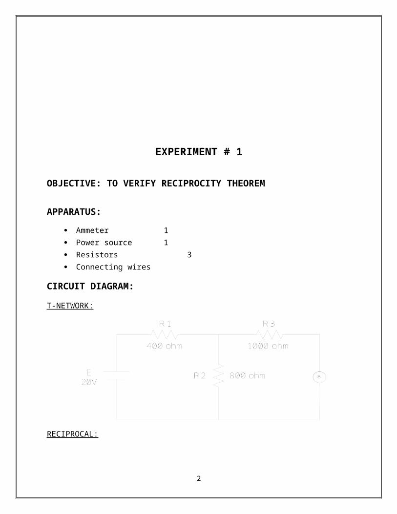
OBJECTIVE: TO VERIFY RECIPROCITY THEOREM
APPARATUS:
Ammeter 1 Power source 1 Resistors 3 Connecting wires
CIRCUIT DIAGRAM:
T-NETWORK:
RECIPROCAL:
PIE NETWORK:
2
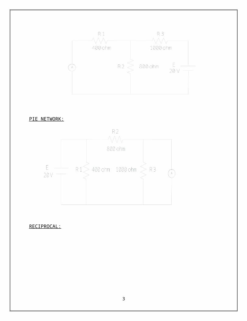
RECIPROCAL:
THEORY:
“In any linear, bilateral single source network, if source of emf E in any branch produces a current I in any other branch, then the same emf E acting in second branch will produce the same current I in the first branch.”In other words, it simply means that E and I are mutually transferable. The ratio E/I is known as transfer resistance or impedance (Z) in AC networks. An other way of stating the above theorem is that the receiving point and sending point in a network are interchangeable.
When applying reciprocity theorem for a voltage source, following steps must be taken:- Voltage source is replaced by a short circuit in original location
3
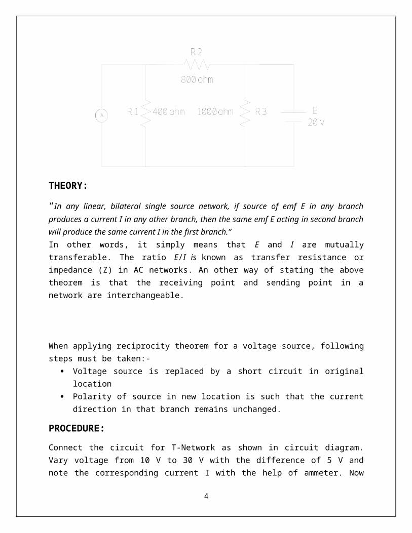
Polarity of source in new location is such that the current direction in that branch remains unchanged.
PROCEDURE:
Connect the circuit for T-Network as shown in circuit diagram. Vary voltage from 10 V to 30 V with the difference of 5 V and note the corresponding current I with the help of ammeter. Now interchange the positions of ammeter and power supply to obtain the reciprocal T-Network. Again repeat the same procedure and note current I’. Calculate the percentage error (%E).Connect the same resistances in PIE-Network and repeat the same procedure and calculate currents I, I’ and %E.
OBSERVATIONS & CALCULATIONS:
T-NETWORK:
Sr. No. E I I’ %E(Volts) (Ampere) (Ampere)
1 102 153 204 25
PIE-NETWORK:
Sr. No. E I I’ %E(Volts) (Ampere) (Ampere)
1 102 153 204 25
CONCLUSION & COMMENTS:________________________________________________________________________________________________________________________________________________________________________________________________________________________________________________________________________
PRECAUTIONS:
4
While dealing with electric circuits handle the apparatus carefully. Make sure the connections are tight. Observe the readings carefully.
EXPERIMENT # 2
5

OBJECTIVE: TO STUDY MAXIMUM POWER TRANSFER THEOREM
APPARATUS:
Power source 1 Resistors 2 Voltmeter 1 Connecting wires
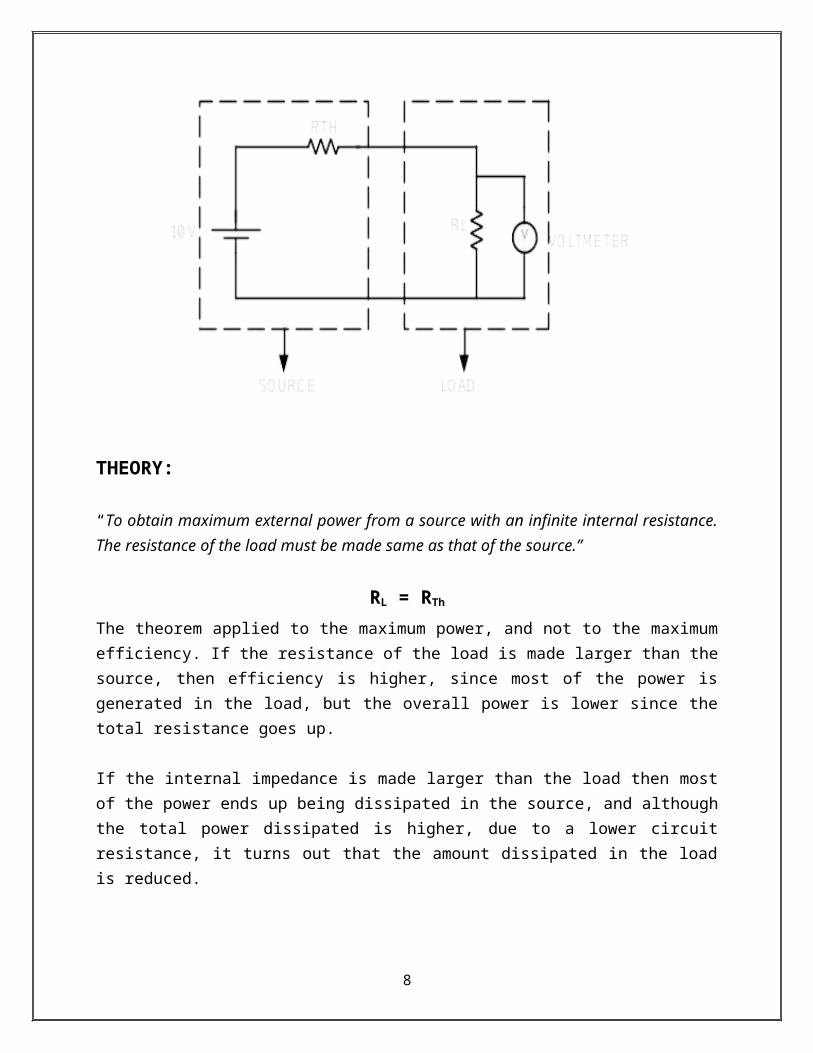
CIRCUIT DIAGRAM:
THEORY:
“To obtain maximum external power from a source with an infinite internal resistance. The resistance of the load must be made same as that of the source.”
RL = RTh
The theorem applied to the maximum power, and not to the maximum efficiency. If the resistance of the load is made larger than the source, then efficiency is higher, since most of the power is generated in the load, but the overall power is lower since the total resistance goes up.
6
If the internal impedance is made larger than the load then most of the power ends up being dissipated in the source, and although the total power dissipated is higher, due to a lower circuit resistance, it turns out that the amount dissipated in the load is reduced.
The condition of maximum power transfer does not result in maximum efficiency. If we define
the efficiency η as the ratio of power dissipated by the load to power developed by the source, then
Consider three particular cases:
If , then If or , then
If , then
The efficiency is only 50% when maximum power transfer is achieved, but approaches 100% as the load resistance approaches infinity (or the source resistance approaches zero), though the total power level tends towards zero. When the load resistance is zero, all the power is consumed inside the source (the power dissipated in a short circuit is zero) so the efficiency is zero.
PROCEDURE:
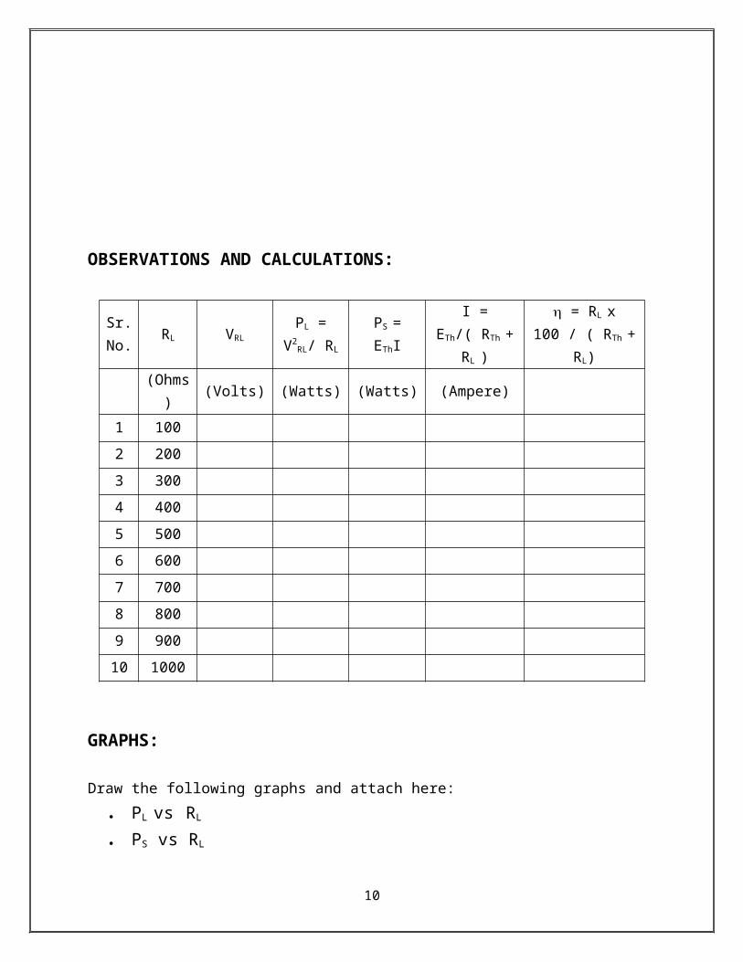
Connect source voltage, thevenin resistance, load resistance and voltmeter as shown in circuit
diagram. Vary the load resistance from 100 to 1000 in steps of 100. Find VRL, PL, PS, I and. Note the readings in the table. Now according to theorem to obtain maximum power transfer from source to load, vary load resistance such that it is equal to the thevenin resistance.
7
OBSERVATIONS AND CALCULATIONS:
Sr. No.
RL VRLPL = V2
RL/ RL
PS = EThII = ETh/( RTh +
RL ) = RL x 100 /
( RTh + RL)
(Ohms) (Volts) (Watts) (Watts) (Ampere)
1 100
2 200
3 300
4 400
5 500
6 600
7 700
8 800
9 900
10 1000
GRAPHS:
Draw the following graphs and attach here:
PL vs RL
PS vs RL
VRL vs RL
IL vs RL
vs RL
CONCLUSION & COMMENTS:________________________________________________________________________________________________________________________________________________________________________________________________________________________________________________________________________
PRECAUTIONS:
While dealing with electric circuits handle the apparatus carefully.
8

Make sure the connections are tight. Observe the readings carefully.
EXPERIMENT # 3
OBJECTIVE: TO STUDY STAR DELTA TRANSFORMATION
APPARATUS: Power Source 1 Ammeter 1 Resistors 3 Connecting Wires
CIRCUIT DIAGRAM:
9
THEORY:
“Star-delta transformation is a mathematical technique to simplify the analysis of an electrical network”
Delta Connections Star Connections
The transformation is used to establish equivalence for networks with 3 terminals. Where three elements terminate at a common node and none are sources, the node is eliminated by transforming the impedances. For equivalence, the impedance between any pair of terminals must be the same for both networks and hence the current through any pair of nodes must be same for both networks. The equations given here are valid for real as well as complex impedances.
Equations for transformation from Δ-Load to Y-load are as follows:
Equations for transformation from Y-load to Δ-load are as follows:
10
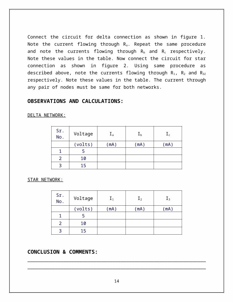
PROCEDURE:
Connect the circuit for delta connection as shown in figure 1. Note the current flowing through Ra. Repeat the same procedure and note the currents flowing through Rb and Rc respectively. Note these values in the table. Now connect the circuit for star connection as shown in figure 2. Using same procedure as described above, note the currents flowing through R1, R2 and R3Z
respectively. Note these values in the table. The current through any pair of nodes must be same for both networks.
OBSERVATIONS AND CALCULATIONS:
DELTA NETWORK:
Sr. No. Voltage Ia Ib Ic
(volts) (mA) (mA) (mA)1 5
2 10
3 15
STAR NETWORK:
Sr. No. Voltage I1 I2 I3
(volts) (mA) (mA) (mA)
1 5
2 10
3 15
CONCLUSION & COMMENTS:________________________________________________________________________________________________________________________________________________________________________________________________________________________________________________________________________________________________________________________
11

PRECAUTIONS:
While dealing with electric circuits handle the apparatus carefully. Make sure the connections are tight. Observe the readings carefully.
12

EXPERIMENT # 4
OBJECTIVE: TO STUDY THE CHARACTERISTICS OF RC SERIES CIRUIT
APPARATUS:
Power Source 1 Capacitor 1 Resistor 1 Square wave generator 1 Oscilloscope 1 Connecting wires
CIRCUIT DIAGRAM:
THEORY:
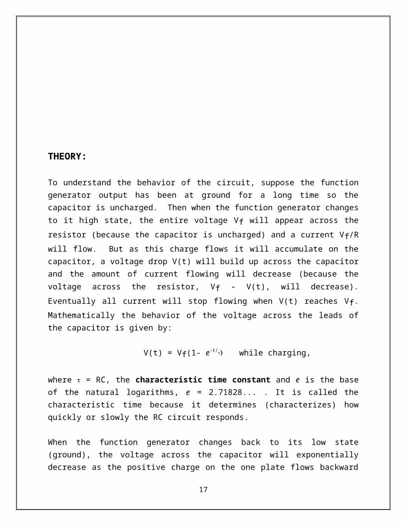
To understand the behavior of the circuit, suppose the function generator output has been at ground for a long time so the capacitor is uncharged. Then when the function generator changes to it high state, the entire voltage Vf will appear across the resistor (because the capacitor is
uncharged) and a current Vf/R will flow. But as this charge flows it will accumulate on the
capacitor, a voltage drop V(t) will build up across the capacitor and the amount of current flowing will decrease (because the voltage across the resistor, Vf - V(t), will decrease).
13
Eventually all current will stop flowing when V(t) reaches Vf. Mathematically the behavior of
the voltage across the leads of the capacitor is given by:
V(t) = Vf(1- e-t/ while charging,
where = RC, the characteristic time constant and e is the base of the natural logarithms, e = 2.71828... . It is called the characteristic time because it determines (characterizes) how quickly or slowly the RC circuit responds.
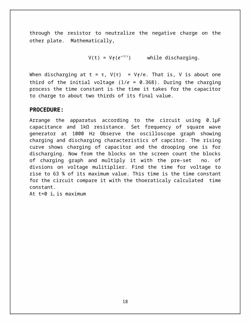
When the function generator changes back to its low state (ground), the voltage across the capacitor will exponentially decrease as the positive charge on the one plate flows backward through the resistor to neutralize the negative charge on the other plate. Mathematically,
V(t) = Vf(e-t/τ) while discharging.
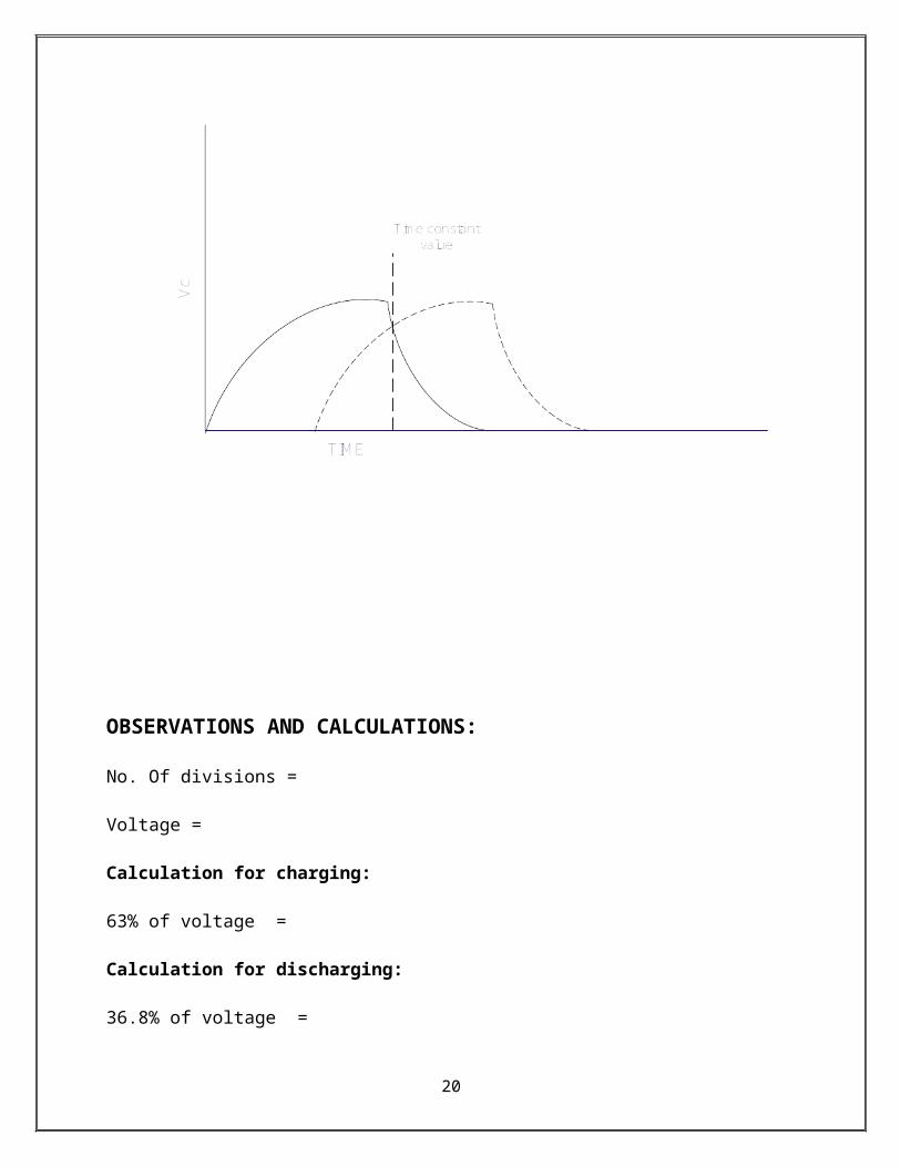
When discharging at t = , V() = Vf/e. That is, V is about one third of the initial voltage (1/e = 0.368). During the charging process the time constant is the time it takes for the capacitor to charge to about two thirds of its final value.
PROCEDURE:Arrange the apparatus according to the circuit using 0.1µF capacitance and 1kΩ resistance. Set frequency of square wave generator at 1000 Hz Observe the oscilloscope graph showing charging and discharging characteristics of capcitor. The rising curve shows charging of capacitor and the drooping one is for discharging. Now from the blocks on the screen count the blocks of charging graph and multiply it with the pre-set no. of divsions on voltage mulitiplier. Find the time for voltage to rise to 63 % of its maximum value. This time is the time constant for the circuit compare it with the thoeraticaly calculated time constant.At t=0 ic is maximum
14
To measure time constant shift the axis to the value of voltage obtained.
15

OBSERVATIONS AND CALCULATIONS:
No. Of divisions =
Voltage =
Calculation for charging:
63% of voltage =
Calculation for discharging:
36.8% of voltage =
Time constants:
Theoratical Time constant = R*C =
Observed time constant (from graph) =
CONCLUSION & COMMENTS:
16
________________________________________________________________________________________________________________________________________________________________________________________________________________________________________________________________________
PRECAUTIONS:
Read graph carefully from oscilloscope. Make sure the connections are tight. Observe the readings carefully.
EXPERIMENT # 5
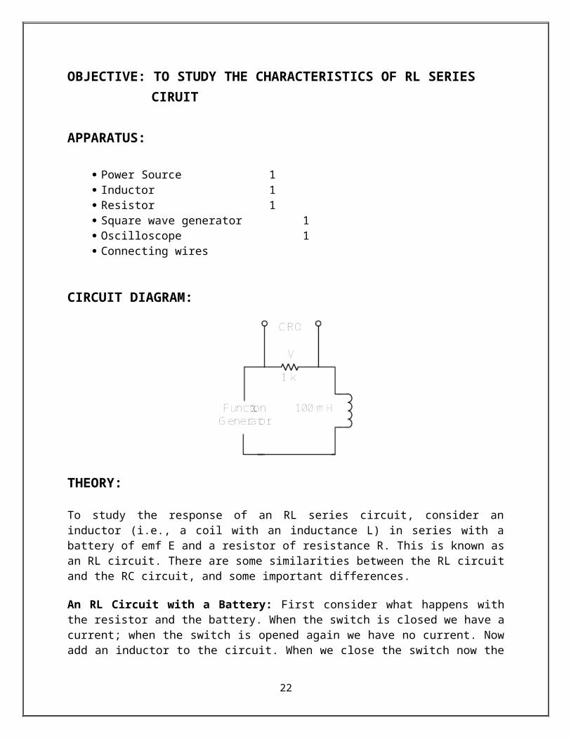
OBJECTIVE: TO STUDY THE CHARACTERISTICS OF RL SERIES CIRUIT
APPARATUS:
Power Source 1 Inductor 1 Resistor 1 Square wave generator 1 Oscilloscope 1 Connecting wires
17
CIRCUIT DIAGRAM:
THEORY:
To study the response of an RL series circuit, consider an inductor (i.e., a coil with an inductance L) in series with a battery of emf E and a resistor of resistance R. This is known as an RL circuit. There are some similarities between the RL circuit and the RC circuit, and some important differences.
An RL Circuit with a Battery: First consider what happens with the resistor and the battery. When the switch is closed we have a current; when the switch is opened again we have no current. Now add an inductor to the circuit. When we close the switch now the current tries to jump up to the same value we had with the resistor but the inductor opposes this because a change in current means a change in flux for the coil. If the inductor adds negligible resistance to the circuit the current eventually reaches the same value it had with the resistor but the current follows an exponential curve to get there.
To see why, apply Kirchoff's loop rule. With the switch closed we have:
E - IR - L dI/dt = 0
Solving this for current gives
I(t) = Io [1 - e-t/τ ]
where Io = E/R is the maximum current and the time constant τ = L/R
The potential difference across the resistor has a similar form:
VR = E [1 - e-t/τ]
The potential difference across the inductor is:
18

VL = E e-t/τ
The graph of current as a function of time in the RL circuit has the same form as the graph of the capacitor voltage as a function of time in the RC circuit, while the graph of the inductor voltage as a function of time in the RL circuit has the same form as the graph of current vs. time in the RC circuit.
An RL Circuit without a Battery: If we take our previous circuit, wait for a while for the current to level off, and then open the switch so the battery is no longer in the circuit, what happens. If the circuit had just a resistor the current would drop immediately to zero. With the inductor the change in current means a change in magnetic flux so the inductor opposes the
change. The current does eventually reach zero but it takes some time to get there.
To see why, apply Kirchoff's loop rule. With the switch opened we have:
IR + L dI/dt = 0
dI/dt = -IR/L
Solving this for current gives
I(t) = Io e-t/τ
The potential difference across the resistor has a similar form:
VR = E e-t/τ
The potential difference across the inductor is negative because it's acting like a battery hooked up in the opposite direction:
VL = -E e-t/τ
Once again, the graph of current as a function of time in the RL circuit has the same form as the graph of the capacitor voltage as a function of time in the discharging RC circuit, while the graph of the inductor voltage as a function of time in the RL circuit has the same form as the graph of current vs. time in the discharging RC circuit.
PROCEDURE:
Connect the circuit according to the circuit diagram. Set frequency of square wave generator. Observe the oscilloscope graph showing voltage across resistor. Now from the blocks on the screen count the blocks of rising graph and multiply it with the pre-set no. of divsions on voltage mulitiplier. Find the time for voltage to rise to 63 % of its maximum value. This time is the time constant for the circuit compare it with the thoeraticaly calculated time constant.
19
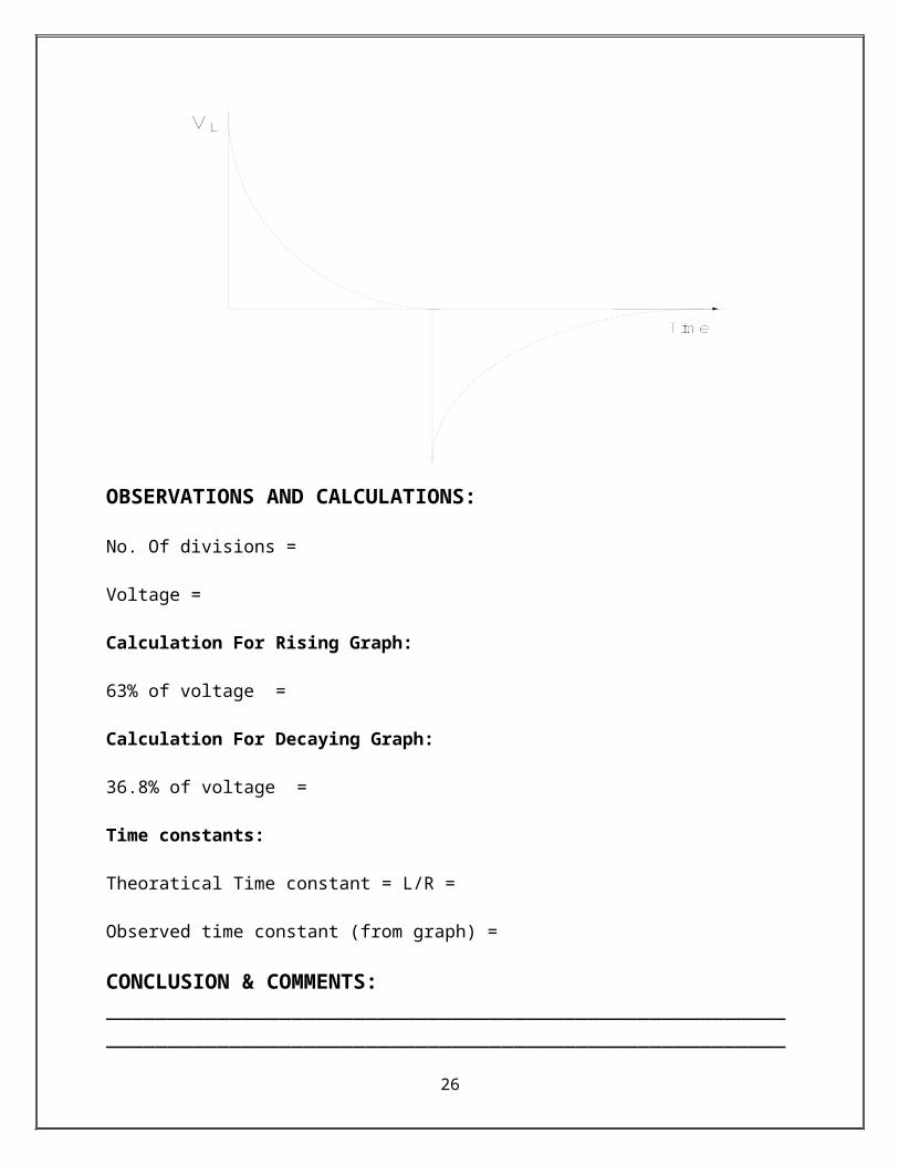
OBSERVATIONS AND CALCULATIONS:
20
No. Of divisions =
Voltage =
Calculation For Rising Graph:
63% of voltage =
Calculation For Decaying Graph:
36.8% of voltage =
Time constants:
Theoratical Time constant = L/R =
Observed time constant (from graph) =
CONCLUSION & COMMENTS:________________________________________________________________________________________________________________________________________________________________________________________________________________________________________________________________________
PRECAUTIONS:
Read graph carefully from oscilloscope. Make sure the connections are tight. Observe the readings carefully.
EXPERIMENT # 6
OBJECTIVE: FIND THE RESONANCE FREQUENCY IN RLC SERIES CIRCUIT
APPARATUS:
Power Source 1 Function generator 1 Resistor 1 Capacitor 1 Inductor 1 Oscilloscope 1 Connecting Wires
21
CIRCUIT DIAGRAM:
THEORY:
A resonant circuit, also called a tuned circuit consists of an inductor and a capacitor together with a voltage or current source. It is one of the most important circuits used in electronics. For example, a resonant circuit, in one of its many forms, allows us to select a desired radio or television signal from the vast number of signals that are around us at any time.
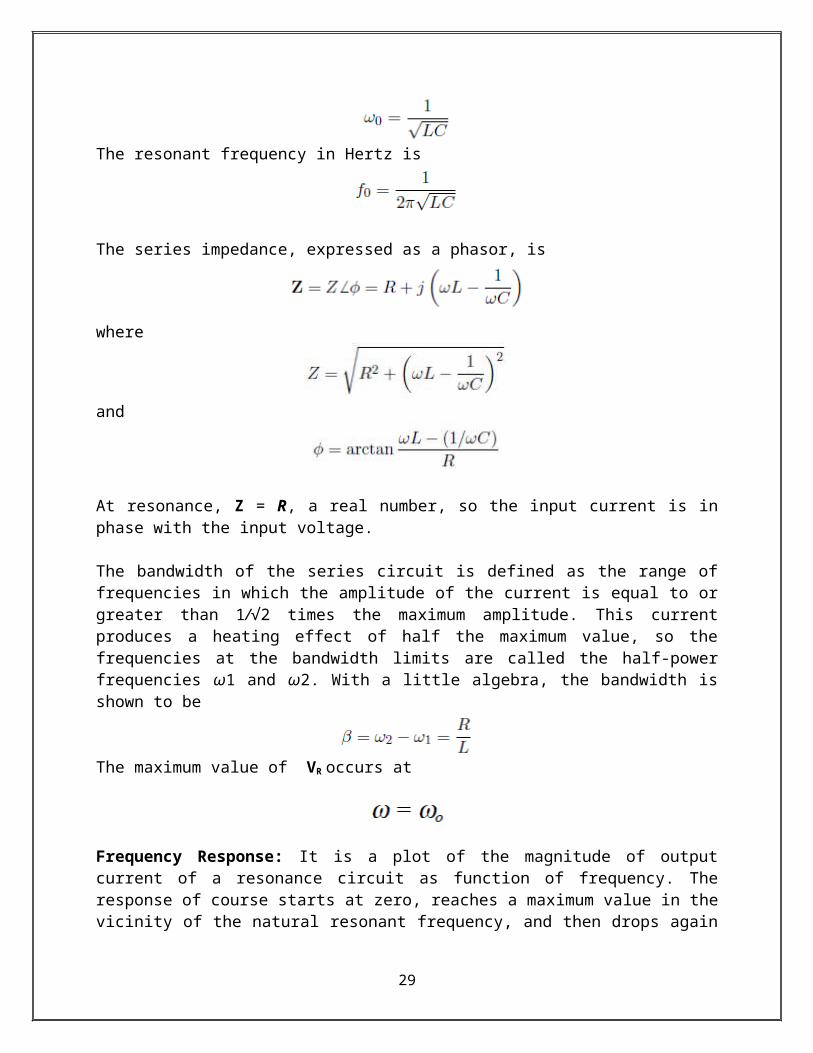
A network is in resonance when the voltage and current at the network input terminals are in phase and the input impedance of the network is purely resistive. The frequency at which the reactances of the inductance and the capacitance cancel each other is the resonant frequency (or the unity power factor frequency) of this circuit.
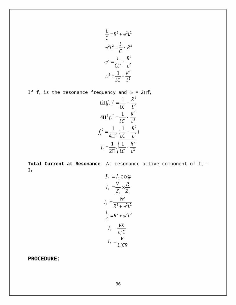
The voltage across the inductor leads the current through the inductor by 90o, while the voltage across the capacitor lags the current by 90o. The two voltages tend to cancel each other, and actually do cancel at the resonant frequency ω0, as defined by
We then solve for the resonant frequency in radians per second as
The resonant frequency in Hertz is
22
The series impedance, expressed as a phasor, is
where
and
At resonance, Z = R, a real number, so the input current is in phase with the input voltage.
The bandwidth of the series circuit is defined as the range of frequencies in which the amplitude of the current is equal to or greater than 1/√2 times the maximum amplitude. This current produces a heating effect of half the maximum value, so the frequencies at the bandwidth limits are called the half-power frequencies ω1 and ω2. With a little algebra, the bandwidth is shown to be
The maximum value of VR occurs at
Frequency Response: It is a plot of the magnitude of output current of a resonance circuit as function of frequency. The response of course starts at zero, reaches a maximum value in the vicinity of the natural resonant frequency, and then drops again to zero as ω becomes infinite. The frequency response is shown in figure.
23
Frequency response of series RLC circuit
PROCEDURE: Connect the circuit as shown in circuit diagram. Apply different frequencies to the series RLC circuit using function generator. Calculate the values of capacitive reactance, inductive reactance and total impedance ‘Z’ and note these values in table. Also note the current flowing through the circuit for each frequency applied. The frequency at which the current through the circuit is maximum and the total impedance of the circuit is minimum will be the resonance frequency.
OBSERVATIONS AND CALCULATIONS:
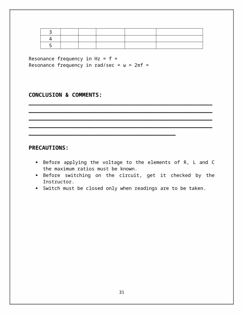
Sr. No. f I XL=2πfL XC=1/(2πfC) Z=√(R2+(XL-XC)2)(Hz) (A)
12345
Resonance frequency in Hz = f = Resonance frequency in rad/sec = ω = 2πf =
CONCLUSION & COMMENTS:
24

________________________________________________________________________________________________________________________________________________________________________________________________________________________________________________________________________
PRECAUTIONS:
Before applying the voltage to the elements of R, L and C the maximum ratios must be known.
Before switching on the circuit, get it checked by the Instructor. Switch must be closed only when readings are to be taken.
EXPERIMENT # 7
25
OBJECTIVE: FIND THE RESONANCE FREQUENCY IN RLC SERIES PARALLEL CIRCUIT (TANK CIRCUIT)
APPARATUS:
Power Source 1 Function generator 1 Resistor 1 Capacitor 1 Inductor 1 Connecting Wires
CIRCUIT DIAGRAM:
THEORY:
The tank circuit, a common building block in electronic systems, is a parallel resonant circuit comprised of an inductor, a capacitor, and an optional resistor. Since the capacitor and the inductor both store energy, this type of circuit is referred to as a tank circuit.
An LC circuit can store electrical energy vibrating at its resonant frequency. A capacitor stores energy in the electric field between its plates, depending on the voltage across it, and an inductor stores energy in its magnetic field, depending on the current through it.
If a charged capacitor is connected across an inductor, charge will start to flow through the inductor, building up a magnetic field around it, and reducing the voltage on the capacitor. Eventually all the charge on the capacitor will be gone. However, the current will continue, because inductors resist changes in current, and energy will be extracted from the magnetic field to keep it flowing. The current will begin to charge the capacitor with a voltage of opposite polarity to its original charge. When the magnetic field is completely dissipated the current will stop and the charge will again be stored in the capacitor (with the opposite polarity). Then the cycle will begin again, with the current flowing in the opposite direction through the inductor.
The charge flows back and forth between the plates of the capacitor, through the inductor. The energy oscillates back and forth between the capacitor and the inductor until (if not replenished by power from an external circuit) internal resistance makes the oscillations die out. Its action, known mathematically as a
26
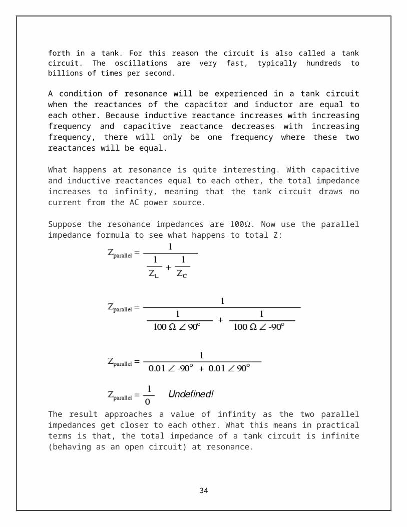
harmonic oscillator, is similar to a pendulum swinging back and forth, or water sloshing back and forth in a tank. For this reason the circuit is also called a tank circuit. The oscillations are very fast, typically hundreds to billions of times per second.
A condition of resonance will be experienced in a tank circuit when the reactances of the capacitor and inductor are equal to each other. Because inductive reactance increases with increasing frequency and capacitive reactance decreases with increasing frequency, there will only be one frequency where these two reactances will be equal.
What happens at resonance is quite interesting. With capacitive and inductive reactances equal to each other, the total impedance increases to infinity, meaning that the tank circuit draws no current from the AC power source.
Suppose the resonance impedances are 100. Now use the parallel impedance formula to see what happens to total Z:
The result approaches a value of infinity as the two parallel impedances get closer to each other. What this means in practical terms is that, the total impedance of a tank circuit is infinite (behaving as an open circuit) at resonance.
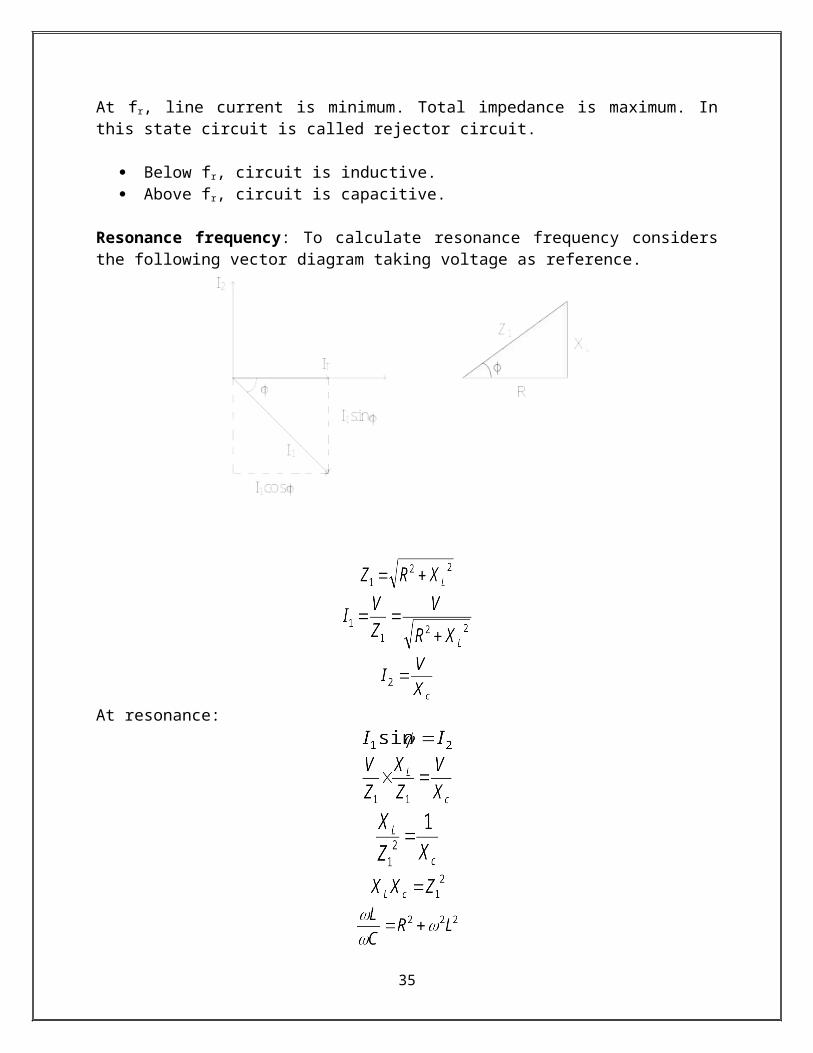
At fr, line current is minimum. Total impedance is maximum. In this state circuit is called rejector circuit.
Below fr, circuit is inductive. Above fr, circuit is capacitive.
Resonance frequency: To calculate resonance frequency considers the following vector diagram taking voltage as reference.
27

At resonance:
If fr is the resonance frequency and = 2fr
28
Total Current at Resonance: At resonance active component of I1 = IT
PROCEDURE:
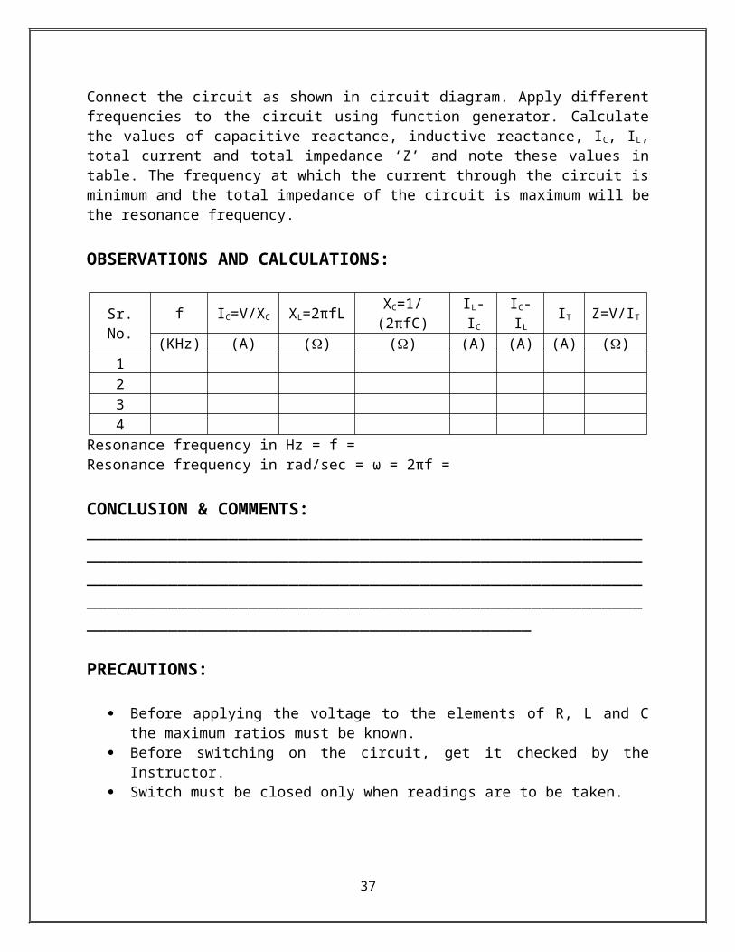
Connect the circuit as shown in circuit diagram. Apply different frequencies to the circuit using function generator. Calculate the values of capacitive reactance, inductive reactance, IC, IL, total current and total impedance ‘Z’ and note these values in table. The frequency at which the current through the circuit is minimum and the total impedance of the circuit is maximum will be the resonance frequency.
OBSERVATIONS AND CALCULATIONS:
Sr. No.f IC=V/XC XL=2πfL XC=1/(2πfC) IL-IC IC-IL IT Z=V/IT
(KHz) (A) () () (A) (A) (A) ()1234
Resonance frequency in Hz = f = Resonance frequency in rad/sec = ω = 2πf =
CONCLUSION & COMMENTS: ____________________________________________________________________________________________________________________________________
29

____________________________________________________________________________________________________________________________________
PRECAUTIONS:
Before applying the voltage to the elements of R, L and C the maximum ratios must be known.
Before switching on the circuit, get it checked by the Instructor. Switch must be closed only when readings are to be taken.
EXPERIMENT # 8
OBJECTIVE: TO OBSERVE DAMPING IN RLC SERIES CIRCUIT
APPARATUS:
30
Power Source 1 Function generator 1 Resistor 1 Capacitor 1 Inductor 1 Oscilloscope 1 Connecting Wires
CIRCUIT DIAGRAM:
THEORY:
Resistor-inductor-capacitor (RLC) circuits are second-order circuits. The response of the RLC circuit can be determined using basic circuit analysis. By KVL,
. (1)
The current i through the inductor is the same as the current through the capacitor. The current i through the capacitor is related to the capacitor voltage by
. (2)
The voltage drop across the resistor is
(3)
and the voltage drop across the inductor is given by
31
. (4)
Substituting Equations (3) and (4) into (1) yields
. (5)
Dividing (5) by LC yields
. (6)
The coefficients in (6) are equated to parameters given by
. (7 a & b)
The parameter α is the damping coefficient and the parameter ω0 is the undamped resonant frequency. By substitution,
. (8)
The complementary solution of (8) takes the form
(9)
From which we find the characteristic equation
(10)
Solve for the roots, s1 and s2, of the characteristic equation:
As:
then
32

We define the damping ratio parameter to be
(11)
Following are the different types of responses obtained by changing value of ζ
Case 1: The Overdamped Response (ζ > 1, α > ω0, R > RCR)
The roots are negative, real and distinct: (a1/2a2)2 > (a0/ a2)The solution is simply
Case 2: The Critically Damped Response (ζ = 1, α = ω0, R = RCR)
The roots are negative, real and indistinct: (a1/2a2)2 = (a0/ a2)So for this case the solution is:
Case 3: The Underdamped Response (ζ < 1, α < ω0, R < RCR)
The roots are distinct and complex: (a1/2a2)2 < (a0/ a2)The solution is simply:
Case 4: The Undamped Response (ζ = 0, α = 0, R = 0)
The roots are purely imagenary.The solution is simply:
33
xn(t)= A1es1t + A2es2t where
xn (t) = (A1 + A2t) est where
xn(t) = est (A1 cos dt + A2sindt ) where and d =
xn(f) = A1cosdt + A2sindt where s1,2 =
PROCEDURE:
Connect the circuit as shown in circuit diagram. Suppose resonance frequency be 5KHz and inductance be 100mH. Find capacitance using following relation:
Calculate RCR using following equation:
Now vary R and observe the type of response on oscilloscope. Following types of response will be observed depending on R.
When R > RCR, response will be overdamped. When R = RCR, response will be critically damped. When R < RCR, response will be underdamped. When R = 0, response will be undamped. In this case observe response across L or C.
OBSERVATIONS AND CALCULATIONS:
fr = L = C =RCR =
Sr. No.R
Type of Response()
1234
CONCLUSION & COMMENTS: ____________________________________________________________________________________________________________________________________
34
____________________________________________________________________________________________________________________________________
PRECAUTIONS:
Before applying the voltage to the elements of R, L and C the maximum ratios must be known.
Before switching on the circuit, get it checked by the Instructor. Switch must be closed only when readings are to be taken.
EXPERIMENT # 9
OBJECTIVE: POWER FACTOR IMPROVEMENT
35
APPARATUS:
Power Source 1 Resistor 1 Capacitor 1 Inductor 1 Wattmeter 1 Voltmeter 1 Ammeter 1 Connecting Wires
CIRCUIT DIAGRAM:
THEORY:
The power factor of an AC electric power system is defined as the ratio of the real power flowing to the load to the apparent power, and is a number between 0 and 1 (frequently expressed as a percentage, e.g. 0.5 pf = 50% pf). Real power is the capacity of the circuit for performing work in a particular time. Apparent power is the product of the current and voltage of the circuit. Due to energy stored in the load and returned to the source, or due to a non-linear load that distorts the wave shape of the current drawn from the source, the apparent power can be greater than the real power.
In an electric power system, a load with low power factor draws more current than a load with a high power factor for the same amount of useful power transferred. The higher currents increase the energy lost in the distribution system, and require larger wires and other equipment. Because of the costs of larger equipment and wasted energy, electrical utilities will usually charge a higher cost to industrial or commercial customers where there is a low power factor.
Linear loads with low power factor (such as induction motors) can be corrected with a passive network of capacitors or inductors. The devices for correction of power factor may be at a central substation, or spread out over a distribution system, or built into power-consuming equipment.
36
Circuits containing purely resistive heating elements (filament lamps, strip heaters, cooking stoves, etc.) have a power factor of 1.0. Circuits containing inductive or capacitive elements (electric motors, solenoid valves, lamp ballasts, and others ) often have a power factor below 1.0.
AC power flow has the three components: real power (P), measured in watts (W); apparent power (S), measured in volt-amperes (VA); and reactive power (Q), measured in reactive volt-amperes (var).
The power factor is defined as:
.
In the case of a perfectly sinusoidal waveform, P, Q and S can be expressed as vectors that form a vector triangle such that:
If φ is the phase angle between the current and voltage, then the power factor is equal to , and:
Since the units are consistent, the power factor is by definition a dimensionless number between 0 and 1. When power factor is equal to 0, the energy flow is entirely reactive, and stored energy in the load returns to the source on each cycle. When the power factor is 1, all the energy supplied by the source is consumed by the load. Power factors are usually stated as "leading" or "lagging" to show the sign of the phase angle.
Power factor correction: It is often desirable to adjust the power factor of a system to near 1.0. This power factor correction (PFC) is achieved by switching in or out banks of inductors or capacitors. For example the inductive effect of motor loads may be offset by locally connected capacitors. When reactive elements supply or absorb reactive power near the load, the apparent power is reduced.
Power factor correction may be applied by an electrical power transmission utility to improve the stability and efficiency of the transmission network. Correction equipment may be installed by individual electrical customers to reduce the costs charged to them by their electricity supplier. A high power factor is generally desirable in a transmission system to reduce transmission losses and improve voltage regulation at the load.
37
Power factor correction brings the power factor of an AC power circuit closer to 1 by supplying reactive power of opposite sign, adding capacitors or inductors which act to cancel the inductive or capacitive effects of the load, respectively. For example, the inductive effect of motor loads may be offset by locally connected capacitors. If a load had a capacitive value, inductors (also known as reactors) are connected to correct the power factor. In the electricity industry, inductors are said to consume reactive power and capacitors are said to supply it, even though the reactive power is actually just moving back and forth on each AC cycle.
PROCEDURE:
Connect the circuit as shown in circuit diagram. Close switch 1 and open switch 2. Note the readings in the table. Now close switch 2 and vary the capacitance. Note corresponding readings and observe the effect of capacitor on power factor. IC increases with capacitance and as a result power factor is improved.
OBSERVATIONS AND CALCULATIONS:
Sr. No.V I W
cosΦ=W/VIIC IL
(Volts) (A) (Watt) (A) (A)12345
CONCLUSION & COMMENTS: ________________________________________________________________________________________________________________________________________________________________________________________________________________________________________________________________________
PRECAUTIONS:
Before applying the voltage to the elements of R, L and C the maximum ratios must be known.
Before switching on the circuit, get it checked by the Instructor. Switch must be closed only when readings are to be taken.
38
Related Documents