My First Five PSoC ® 3 Designs By Robert Ashby Spec. # 001-58878 Rev. *C Cypress Semiconductor 198 Champion Court San Jose, CA 95134-1709 Phone (USA): 800.858.1810 Phone (Intnl): 408.943.2600 http://www.cypress.com

My First Five PSoC® 3 Designs_001-58878
Oct 30, 2014
Welcome message from author
This document is posted to help you gain knowledge. Please leave a comment to let me know what you think about it! Share it to your friends and learn new things together.
Transcript

My First Five PSoC® 3 Designs
By Robert Ashby
Spec. # 001-58878 Rev. *C
Cypress Semiconductor198 Champion Court
San Jose, CA 95134-1709
Phone (USA): 800.858.1810Phone (Intnl): 408.943.2600
http://www.cypress.com

2 My First Five PSoC 3 Designs, Spec. # 001-58878 Rev. *C
Copyrights
Copyrights
© Cypress Semiconductor Corporation, 2010-2012. The information contained herein is subject to change without notice.Cypress Semiconductor Corporation assumes no responsibility for the use of any circuitry other than circuitry embodied in aCypress product. Nor does it convey or imply any license under patent or other rights. Cypress products are not warrantednor intended to be used for medical, life support, life saving, critical control or safety applications, unless pursuant to anexpress written agreement with Cypress. Furthermore, Cypress does not authorize its products for use as critical componentsin life-support systems where a malfunction or failure may reasonably be expected to result in significant injury to the user.The inclusion of Cypress products in life-support systems application implies that the manufacturer assumes all risk of suchuse and in doing so indemnifies Cypress against all charges.
Trademarks
PSoC Creator™ is a trademark and PSoC® and CapSense® are registered trademarks of Cypress Semiconductor Corp. Allother trademarks or registered trademarks referenced herein are property of the respective corporations.
Source Code
Any Source Code (software and/or firmware) is owned by Cypress Semiconductor Corporation (Cypress) and is protected byand subject to worldwide patent protection (United States and foreign), United States copyright laws and international treatyprovisions. Cypress hereby grants to licensee a personal, non-exclusive, non-transferable license to copy, use, modify, createderivative works of, and compile the Cypress Source Code and derivative works for the sole purpose of creating custom soft-ware and or firmware in support of licensee product to be used only in conjunction with a Cypress integrated circuit as speci-fied in the applicable agreement. Any reproduction, modification, translation, compilation, or representation of this SourceCode except as specified above is prohibited without the express written permission of Cypress.
Disclaimer
CYPRESS MAKES NO WARRANTY OF ANY KIND, EXPRESS OR IMPLIED, WITH REGARD TO THIS MATERIAL,INCLUDING, BUT NOT LIMITED TO, THE IMPLIED WARRANTIES OF MERCHANTABILITY AND FITNESS FOR A PAR-TICULAR PURPOSE. Cypress reserves the right to make changes without further notice to the materials described herein.Cypress does not assume any liability arising out of the application or use of any product or circuit described herein. Cypressdoes not authorize its products for use as critical components in life-support systems where a malfunction or failure may rea-sonably be expected to result in significant injury to the user. The inclusion of Cypress' product in a life-support systems appli-cation implies that the manufacturer assumes all risk of such use and in doing so indemnifies Cypress against all charges.
Use may be limited by and subject to the applicable Cypress software license agreement.

My First Five PSoC 3 Designs, Spec. # 001-58878 Rev. *C 3
Contents
1. Introducing the PSoC® 3/PSoC 5 Architecture 5
1.1 Beyond Microcontrollers ..............................................................................................51.1.1 Content and Organization ................................................................................5
1.2 Microcontroller Basics..................................................................................................61.2.1 The CPU ..........................................................................................................61.2.2 Memories .........................................................................................................61.2.3 Peripherals .......................................................................................................7
1.3 Features of the PSoC 3 and PSoC 5 Architectures.....................................................71.4 Conventions...............................................................................................................131.5 Revision History ........................................................................................................13
2. CY8C38xxx Introduction 152.1 CY8C38xxx................................................................................................................152.2 DVK1 Board...............................................................................................................172.3 PSoC Creator™.........................................................................................................18
2.3.1 Workspace Explorer .......................................................................................192.3.2 Design-Wide Resources ................................................................................212.3.3 Schematic View..............................................................................................212.3.4 Source Files and Header Files.......................................................................22
2.4 Example Designs.......................................................................................................22
3. Learn By Example: Blink an LED 23
3.1 Project Overview........................................................................................................233.2 Background Information.............................................................................................233.3 Project Steps .............................................................................................................24
3.3.1 Starting a New Project....................................................................................243.3.2 Adding Components.......................................................................................25
3.3.2.1 Adding a Clock Component .............................................................253.3.2.2 Adding a PWM Component .............................................................263.3.2.3 Adding a Digital Pin Component ......................................................28
3.3.3 Connecting Components and Chip Resources ..............................................283.3.4 Assigning Pins................................................................................................303.3.5 Code...............................................................................................................313.3.6B:Building and Debugging Your Project.............................................................37
3.4 Conclusions ...............................................................................................................383.5 Additional Information ................................................................................................38
4. Learn By Example: UART 41
4.1 Project Overview........................................................................................................414.2 Background Information.............................................................................................414.3 Project Steps .............................................................................................................42
4.3.1 Adding a New Project.....................................................................................42

4 My First Five PSoC 3 Designs, Spec. # 001-58878 Rev. *C
Contents
4.3.2 Adding Components ......................................................................................434.3.2.1 Adding a Character LCD Component..............................................434.3.2.2 Adding a UART Component ............................................................464.3.2.3 Adding a Digital I/O Component ......................................................49
4.3.3 Assigning Pins ...............................................................................................494.3.4 Configuring Clocks.........................................................................................494.3.5 Code ..............................................................................................................514.3.6 Building and Debugging Your Project ............................................................55
4.4 Conclusions ...............................................................................................................564.5 Additional Information................................................................................................57
5. Learn By Example: CapSense 59
5.1 Project Overview .......................................................................................................595.2 Project Background Information ................................................................................595.3 Operation...................................................................................................................605.4 Project Steps .............................................................................................................60
5.4.1 Adding a Project ............................................................................................605.4.2 Adding and Configuring a CapSense_CSD Component ...............................61
5.4.2.1 Assigning Pins .................................................................................665.4.3 CapSense Code ............................................................................................67
5.5 Conclusions ...............................................................................................................705.6 Additional Information................................................................................................70
6. Learn By Example: Digital Logic 736.1 Project Overview .......................................................................................................736.2 Project Background Information ................................................................................736.3 Project Steps .............................................................................................................73
6.3.1 Adding a Project ............................................................................................736.3.1.1 Setting Up Your Project ...................................................................736.3.1.2 Adding and Configuring a Control Register .....................................746.3.1.3 Using Sheet Connectors..................................................................756.3.1.4 Adding a Lookup Table....................................................................786.3.1.5 Adding More Registers ....................................................................796.3.1.6 Adding a Hardware Delay................................................................79
6.3.2 Code ..............................................................................................................816.4 Conclusions ...............................................................................................................906.5 Additional Information................................................................................................91
7. Learn By Example: Precision Analog 937.1 Project Overview .......................................................................................................937.2 Project Background Information ................................................................................937.3 Project Steps .............................................................................................................93
7.3.1 Adding Components ......................................................................................937.3.2 Configuring Components ...............................................................................977.3.3 Assigning Pins ...............................................................................................977.3.4 Code ..............................................................................................................99
7.4 Conclusion...............................................................................................................1067.5 Additional Information..............................................................................................107
Index 109

My First Five PSoC 3 Designs, Spec. # 001-58878 Rev. *C 5
1. Introducing the PSoC® 3/PSoC 5 Architecture
1.1 Beyond Microcontrollers
Cypress and the PSoC® 3 and PSoC 5 architectures of programmable system-on-chip devices set anew standard for microcontrollers. This new standard is not just a matter of improving upon the com-petition. It is a dramatic paradigm shift and exists in a class by itself. The PSoC 3 and PSoC 5devices perform the functions of a basic microcontroller, but they also do much more. You will learnnew ways of solving problems and new methods of accomplishing your design goals. The ability todesign entire analog systems within one chip, coupled with unparalleled flexibility in signal routingand reconfiguration, creates entirely new possibilities in electronics design.
1.1.1 Content and Organization
This book is a guide to five basic designs:
The designs selected for this book provide you with a working foundation. Each project builds uponthe knowledge you learn from the previous project. By the time you finish the Project 5, you will knowabout the PSoC CY8C38xxx core, its digital peripheral capabilities, and its analog capabilities. Eachcompleted project includes interfaces to user input, display, and computer communication. You willhave created an entire system using a single chip and will realize how easy it is to complete thesedesigns. The Cypress system is perfect for the hobbyist, student, and engineer. The design processis easy enough for a beginner with minimal experience, and powerful enough to stretch the imagina-tion of the most seasoned engineer.
Before discussing a few of the features for the PSoC 3 and PSoC 5 architectures, there is a briefexplanation of Microcontroller Basics on page 6. If you have a good working knowledge of microcon-trollers, you can skip the section.
Project 1Blink an LED
Set up timing structure and set up basic signal input and output.
Project 2UART
Set up a link between your project and the computer. Use the computer as an input and out-put tool to enhance and debug your project.
Project 3CapSense®
Add CapSense buttons and a slider to your project.
Project 4Digital Logic
Create a PSoC simulation of the farmer, fox, goose, corn riddle.
Project 5Precision Analog
Add simple analog processing to your project.
6 My First Five PSoC 3 Designs, Spec. # 001-58878 Rev. *C
Introducing the PSoC® 3/PSoC 5 Architecture
1.2 Microcontroller Basics
Cypress uses the phrase programmable system-on-chip to describe the PSoC platform. The PSoC 3and PSoC 5 devices are often compared with microcontrollers in relation to other devices in theindustry. The PSoC 3 and PSoC 5 devices function similarly to other microcontrollers and performthe same tasks. However, the PSoC 3 and PSoC 5 devices perform functions that are not possible inmany other microcontrollers in the industry. First, however, what is a microcontroller?
If you were to ask several people in the electronics industry to define a microcontroller, you might besurprised by the varying definitions. This exists because the term microcontroller is used to describea wide breadth of devices with very different capabilities and structures. The abilities of microcon-trollers have improved dramatically over the years while the prices have dropped. The key to under-standing what a microcontroller is lies in what these devices have in common rather than how theydiffer.
Embedded system is an industry term used for a design with a microcontroller. The term is usedbecause the various subsystems are embedded within the design itself and are not separate compo-nents that you need to add. A microcontroller is exactly that. It is a collection of subsystems that areembedded into a single chip. There are three main subsystems in the classic definition of a micro-controller:
■ CPU
■ Memories
■ Peripherals
1.2.1 The CPU
The central processing unit (CPU) is the brains of the microcontroller. The CPU has logic that allowsit to decode instructions and move numbers from one location in memory to another. It performsmathematical operations on those numbers such as shifting bits, adding, and subtracting. Somemicrocontroller CPUs are able to multiply and divide numbers. PSoC 3 devices use a very capable8-bit 8051 CPU. PSoC 5 devices use an even more powerful ARM Cortex M3 Processor.
1.2.2 Memories
The memories in a microcontroller contain both data and instructions. Some microcontrollers, includ-ing the PSoC 3 and PSoC 5 devices, can interface with memory that is contained in separatedevices. Memories come in two broad categories; volatile and nonvolatile. Volatile memory loses itscontents when power is removed. Nonvolatile memory retains its contents even when power isremoved. In general, volatile memories are much faster than nonvolatile memories. Another differ-ence between volatile and nonvolatile memories is that all nonvolatile memories wear out. They canonly be erased an rewritten a limited number of times. The endurance value of a nonvolatile memoryis the number of times that it can be erased and programmed without error.
There are three memory types in the PSoC 3 and PSoC 5 architecture: flash, electrically erasableprogrammable read only memory (EEPROM), and random access memory (RAM). Flash andEEPROM are two types of nonvolatile memory. RAM is volatile. Some PSoC 3 and PSoC 5 devicesalso have an extended memory interface (EMIF) that allows you to add additional memory to thedevice if you need to.
Flash memory is your program memory. You might hear it referred to as read only memory (ROM)because it holds your program memory. However, you can erase and reprogram flash memory. Animportant characteristic of flash memory is that it must be erased in blocks. You cannot erase a sin-gle byte at a time. This might be seen as a disadvantage compared to other nonvolatile memories ifyou are storing small amounts of data. Flash data also has a lower endurance value than some othertypes of nonvolatile memory. Wear leveling is a technique that writes the small amounts of data over
My First Five PSoC 3 Designs, Spec. # 001-58878 Rev. *C 7
Introducing the PSoC® 3/PSoC 5 Architecture
several areas in succession to increase the amount of times that you can rewrite the data withoutdamaging the flash memory.
EEPROM is also nonvolatile memory. You can erase and rewrite information on a row-by-row basisto EEPROM. The endurance value of EEPROM is much higher than flash. This makes EEPROMideal for storing nonvolatile information that needs frequent updates and especially for smalleramounts of information.
RAM memory holds data during program execution. It is possible in some microcontrollers, includingthe PSoC 5 architecture, to copy program memory into RAM and execute that program memorywhile still in RAM. The important characteristics to remember about RAM are that you can change itscontents as often as you like and that you can read from and write to RAM very quickly. The endur-ance value of RAM is high enough that this should not be a concern. RAM is a volatile memorymeaning it does not retain its information when the chip is powered down. There are some newertechnologies that provide nonvolatile storage for RAM, but they are not discussed here.
Note The acronyms RAM and ROM are legacy terms that persist today. The names were given toearly devices and reflect the abilities of those types of memory at that time. However, the evolution ofmicrocontroller design has improved the memories. The limitations described by the names areoften defunct. RAM is not the only memory that can be accessed in a random order and not all ROMmemory is read only.
1.2.3 Peripherals
The peripherals in a microcontroller are functions that are performed by the device. Common periph-erals include I/O ports, analog to digital converters (ADCs), universal asynchronous receiver trans-mitters (UARTs), timers, pulse width modulators (PWMs), and many others. Peripheral functionalitybuilt within the microcontroller distinguishes a microcontroller from a microprocessor. A microproces-sor (such as the one found in your computer) does not typically include these peripheral functions,but instead communicates with separate devices that implement the peripheral functions. A micro-controller contains CPU, memories, and peripherals to create a complete embedded system.
1.3 Features of the PSoC 3 and PSoC 5 Architectures
Microcontroller companies try to find the magic mix of CPU, memories, and peripherals that wins themost customers. It is a never ending goal to give users everything that they need while maintaining acost effective solution. There are thousands of choices and alternatives in microcontrollers today.Cypress is not trying to find the perfect mix. Their goal is to give you a flexible controller that youeasily configure into the perfect mix for your specific project, and then you can take that same deviceand reconfigure it again with an entirely new mix for an entirely different project. That is when thepower of PSoC device configurability really appears.
The PSoC 3 and PSoC 5 architectures provide you with a programmable system-on-chip that excelsin precision analog processing and digital flexibility. The PSoC platform offers 8-bit and 32-bit CPUs.The architecture of the digital and analog peripherals is the same, giving the user the ability tochoose the device that achieves the needed performance and the best value. The combination ofanalog and digital systems on the same chip not only allows you to consolidate your design into asmaller physical space, but also keeps those sensitive analog signals tight within the device itself.This secures a new level of noise immunity and environmental stability.
The PSoC 3 and PSoC 5 architectures provide a complete design platform from the ground up forefficiency and flexibility. The architecture of the platform is similar to a spoked wheel. It consists of ahub with spokes that all connect to the hub. The hub at the center of the architecture is called theperipheral hub (PHUB). The PHUB controls the transfer of information on each of the spokes. Thespokes are the advanced high performance bus (AHB) which connects the PHUB to the CPU, mem-ories, and other peripherals in the PSoC. The AHB allows transfers that range from 16 bits to 32 bits
8 My First Five PSoC 3 Designs, Spec. # 001-58878 Rev. *C
Introducing the PSoC® 3/PSoC 5 Architecture
wide, accommodating both the 8 bit and 32 bit CPU options. All transfers on the AHB are initiated bythe CPU or PHUB. The PHUB contains a direct memory access (DMA) controller, allowing thePHUB to manage transfers of data without any need for CPU interaction. The hub configuration ofthe PSoC 3 and PSoC 5 architecture offers some very significant advantages. The separation of thespokes and the multiple channels of the DMA controller allow simultaneous transfers among deviceson different spokes. This allows for efficient and speedy transfers of data.
The analog system of the PSoC 3 and PSoC 5 architectures features very high precision because ofa very low noise floor and a very accurate reference level. I have not seen the analog capabilities ofthe PSoC 3 and PSoC 5 architectures duplicated or matched in any microcontroller, field program-mable gate array (FPGA), or any other standard device. Embedded systems need analog interfacesto connect to the outside world. Reading temperatures, playing music, controlling liquid crystal dis-plays (LCDs), or reading touch pads all require analog processing. The processing of these analogsystems needs more than a simple ADC. These projects require gain stages, filtering, analog outputsignals, and special sensing circuitry. The PSoC 3 and PSoC 5 architectures provide this capabilityin a single chip.
The analog system includes a sigma delta ADC that is capable of 20 bits of resolution and very fastconversion times. A full 20 bits of resolution is fantastic. In a 3.3V system, this means that the ADCreads changes in a signal as small as three millionths of a volt. An ADC with this type of accuracydepends heavily upon the precision reference and the low noise floor. The noise floor is kept verylow by separating the analog power system from the digital system with the PSoC device itself.Power and ground can connect together at the same pin on some devices, but they separate at thebonding pin inside the chip. The internal reference swings less than 0.2% through the device’s volt-age and temperature range.
The digital filter block (DFB) collects data from the ADC block. The DFB is a small digital signal pro-cessing (DSP) engine that operates independently from the CPU. The DFB has its own arithmeticlogic unit (ALU), its own hardware multiplier, and its own RAM. The DFB is configured as a single 64tap filter or as multiple filters with fewer taps, (for example, 4 filters with 16 taps each).
The PSoC 3 and PSoC 5 architectures include uncommitted operational amplifiers, switched cap/continuous time (SC/CT) blocks, and comparators. All of the blocks, including the SC/CT blocks,have an operational amplifier inside.
Note I have seen the term switched cap raise uncertainty and quizzical looks. The concept of aswitched cap analog system is to use capacitors and analog switches to transfer charge in a system.The combination of the switch system and the capacitor acts similarly to a resistor allowing change-able flexible analog designs.
The uncommitted operational amplifiers are usually configured as unity gain buffers. They can alsoroute their input and output pins to GPIO, allowing you to add your own components to constructgain stages, filters, oscillators, and so on. The SC/CT blocks have resistors, capacitors, andswitches that allow you to build gain stages, filters, differential amplifiers, and so on.
The digital to analog converter (DAC) of the PSoC 3 and PSoC 5 architectures operates as either avoltage DAC or a current DAC. It is the means by which you send the DFB output back out to theanalog domain.
The universal digital blocks (UDBs) are the key to the flexible digital system in the PSoC 3 andPSoC 5 architectures. The UDB does not stand alone as an entity, but is part of a larger array thatholds all the UDBs in the system. This array structure allows the UDB to interact with other UDBblocks before consuming resources in the digital systems interface (DSI). The DSI is the connectionthat allows the UDB to send and receive signals from the I/O and other fixed function peripherals inthe chip.

My First Five PSoC 3 Designs, Spec. # 001-58878 Rev. *C 9
Introducing the PSoC® 3/PSoC 5 Architecture
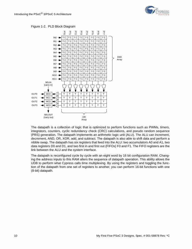
The UDB contains two programmable logic devices (PLDs), a datapath module, and some controland timing logic (see Figure 1-1).
Figure 1-1. UDB Block Diagram
Each PLD is a logic array that accepts 12 inputs into a group of eight product terms (AND function).These product terms are summed (OR function) to provide a 4-bit-wide result. The use of PLD logicdoes not always have to link to the datapath module within that UDB. It can use other UDBs sepa-rate from the datapath module in its own UDB. An example of this situation is if the UDB is config-ured to be an 8-bit timer, then the PLDs are not used for that functionality. In that case, those PLDsare used for other functions if desired. This allows you to fully use all (some limitations exist) thelogic in the UDB array.
PLD 12C4
(8 PTs)
PLD 12C4
(8 PTs)
Datapath
Clock and Reset
Control
Routing Channel
Datapath Chaining
PLD Chaining
Status and Control
10 My First Five PSoC 3 Designs, Spec. # 001-58878 Rev. *C
Introducing the PSoC® 3/PSoC 5 Architecture
Figure 1-2. PLD Block Diagram
The datapath is a collection of logic that is optimized to perform functions such as PWMs, timers,integrators, counters, cyclic redundancy check (CRC) calculations, and pseudo random sequence(PRS) generation. The datapath implements an arithmetic logic unit (ALU). The ALU can increment,decrement, AND, OR, XOR, add, and subtract. The datapath is also able to shift data and perform anibble swap. The datapath has six registers that feed into the ALU: two accumulators A0 and A1, twodata registers D0 and D1, and two first in and first out (FIFOs) F0 and F1. The FIFO registers are thelink between the ALU and the system interface.
The datapath is reconfigured cycle by cycle with an eight word by 16 bit configuration RAM. Chang-ing the address inputs to this RAM alters the sequence of datapath operation. This ability allows theUDB to perform what Cypress calls time multiplexing. By using the registers and toggling the func-tion of the datapath from one set of registers to another, you can perform 16-bit functions with one(8-bit) datapath.
PT
0
IN0
IN1
IN2
IN3
IN4
IN5
IN6
IN7
IN8
IN9
IN10
IN11
T C T C T C T C T C T C T C T C
T C T C T C T C T C T C T C T C
T C T C T C T C T C T C T C T C
T C T C T C T C T C T C T C T C
T C T C T C T C T C T C T C T C
T C T C T C T C T C T C T C T C
T C T C T C T C T C T C T C T C
T C T C T C T C T C T C T C T C
T C T C T C T C T C T C T C T C
T C T C T C T C T C T C T C T C
T C T C T C T C T C T C T C T C
T C T C T C T C T C T C T C T C
PT
1
PT
2
PT
3
PT
4
PT
5
PT
6
PT
7
T T T T T T T T
T T T T T T T T
T T T T T T T T
T T T T T T T T
AND Array
OR Array
MC0
MC1
MC2
OUT0
OUT1
OUT2
OUT3 MC3
SELIN(carry in)
SELOUT(carry out)

My First Five PSoC 3 Designs, Spec. # 001-58878 Rev. *C 11
Introducing the PSoC® 3/PSoC 5 Architecture
Figure 1-3. Datapath Module Block Diagram
The UDBs are arranged in a row and column format referred to as the UDB array. This allows an effi-cient means of signal routing between UDBs. Each UDB is paired with another UDB in the same col-umn. There are 64 I/O lines between these two blocks. These I/O lines connect to the horizontalchannel routes. There are 96 lines in each horizontal channel route. A switch mechanism toggles thesignals from the horizontal channel route to the vertical channel route. There are 32 lines in eachvertical channel route. The vertical channel routes extend beyond the UDBs to connect to the digitalsystem interface.
A0
A1
D0
D1
PI
ALU
Mask
Shift
Data Registers
Output Muxes
F1
F0
FIFOs
Accumulators
PO
A0
A1
D0
D1
Output to Programmable Routing
Chaining
Control S
tore R
AM
8 Wo
rd X 16
Bit
Parallel Input/Output(to/from Programmable Routing)
Input from Programmable
Routing
Input Muxes
To/FromNext Datapath
To/FromPrevious Datapath
Da
tapath
Co
ntro
l
PHUB System Bus
R/W Access to All Registers
Co
nditio
ns: 2
Co
mpa
res, 2 Z
ero D
ete
ct, 2 O
nes
De
tect Overflow
De
tect
66

12 My First Five PSoC 3 Designs, Spec. # 001-58878 Rev. *C
Introducing the PSoC® 3/PSoC 5 Architecture
Figure 1-4. UDB Array Structure
The PSoC 3 and PSoC 5 architectures also include other fixed functions including controller areanetwork (CAN) bus and USB. This platform offers dramatic improvements to existing designs andexciting opportunities for new designs that were not previously possible.
UDB
UDB
UDB
UDB
HVB
UDB
UDB
HVA
UDB
UDB
HVB
HVA
UDB
UDB
UDB
UDB
HVA
UDB
UDB
HVB
UDB
UDB
HVA
HVB
Fix
ed
Fu
nct
ion
I/O
DSI Routing Interface
I/O P
ort
s
Inte
rru
pt
Co
ntr
oll
er
DM
A
Co
ntr
oll
er
Fix
ed
Fu
nctio
n I/O
DSI Routing Interface
I/O P
orts
Interru
pt
Co
ntro
ller
DM
A
Co
ntro
ller
UD
B P
air
Til
e
UD
B A
rra
y C
ore
My First Five PSoC 3 Designs, Spec. # 001-58878 Rev. *C 13
Introducing the PSoC® 3/PSoC 5 Architecture
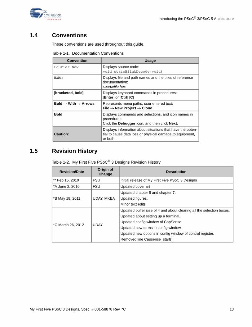
1.4 Conventions
These conventions are used throughout this guide.
1.5 Revision History
Table 1-1. Documentation Conventions
Convention Usage
Courier New Displays source code:void stateBlinkDecode(void)
Italics Displays file and path names and the titles of reference documentation: sourcefile.hex
[bracketed, bold] Displays keyboard commands in procedures:[Enter] or [Ctrl] [C]
Bold With Arrows Represents menu paths, user entered text:File New Project Clone
Bold Displays commands and selections, and icon names in procedures:Click the Debugger icon, and then click Next.
Caution:Displays information about situations that have the poten-tial to cause data loss or physical damage to equipment, or both.
Table 1-2. My First Five PSoC® 3 Designs Revision History
Revision/DateOrigin of Change
Description
** Feb 15, 2010 FSU Initial release of My First Five PSoC 3 Designs
*A June 2, 2010 FSU Updated cover art
*B May 18, 2011 UDAY, MKEA
Updated chapter 5 and chapter 7.
Updated figures.
Minor text edits.
*C March 26, 2012 UDAY
Updated buffer size of 4 and about clearing all the selection boxes.
Updated about setting up a terminal.
Updated config window of CapSense.
Updated new terms in config window.
Updated new options in config window of control register.
Removed line Capsense_start();

14 My First Five PSoC 3 Designs, Spec. # 001-58878 Rev. *C
Introducing the PSoC® 3/PSoC 5 Architecture

My First Five PSoC 3 Designs, Spec. # 001-58878 Rev. *C 15
2. CY8C38xxx Introduction
2.1 CY8C38xxx
The CY8C38xxx family is built on the PSoC® 3 architecture. The CY8C38xxx devices have an 8-bit8051 CPU that runs up to 67 MHz. Most instructions take only one or two cycles to complete. Thepopularity of the 8051 provides a familiar environment for many experienced programmers. Thereare many existing compilers for the 8051 and many free tools and existing code on the Internet thatwere designed for the 8051 and can be used for your CY8C38xxx design.
The 8051 in the CY8C38xxx has enhancements and extra features that were not in the original 8051design. These include an enhanced interrupt controller, instruction cache, and extra pointers. Theenhancements and features allow the 8051 in the CY8C38xxx devices to run faster, with less power,and reduce your code size compared to the original 8051.
The CY8C38xxx has a single sigma delta ADC. The ADC is capable of a maximum 20 bits of resolu-tion while maintaining an 84-dB SINAD (in 16-bit mode). Higher resolution requires longer samplingtime. A conversion of 20-bit resolution can be completed 180 times in a second. Lower resolutionconversion happens much faster. A 16-bit conversion can be completed 48 thousand times per sec-ond. Conversions can be started by a software instruction or by the assertion of a Start of Conver-sion hardware signal that can be triggered from an external source.
There are various modes for the ADC that allow you to capture a single signal, or several differentsignals. The DMA controller allows you to automatically transfer the results of the conversions to theDFB for filtering. The CY8C38xxx offers a single DFB, but that single DFB can be used to constructmultiple filters.
The CY8C38xxx has up to four of each of the following:
■ Comparators
■ Uncommitted opamps
■ SC/CT blocks
■ Voltage/current DACs
These are configurable to provide various components for pure analog processing without processorintervention.
The CY8C38xxx offers up to 24 UDBs. The UDBs are configured automatically when you use theassociated components in PSoC Creator™. However, you can also create your own componentsusing Verilog to configure the digital logic of the UDBs.
The CY8C38xxx features a USB controller and a CAN controller. The USB transceiver provides afull-speed USB peripheral connection with up to eight endpoints. Configuration of the USB trans-ceiver is made much easier with a USB wizard tool included in PSoC Creator. The CAN controllersupports the CAN 2.0 protocol and handles all low-level tasks of the CAN transmission includingmessage separation, CRC checking, CRC calculation, and message buffering.
The CY8C38xxx has up to 62 general purpose input/output (GPIO) pins, eight special input/output(SIO) pins, and two USB pins.
16 My First Five PSoC 3 Designs, Spec. # 001-58878 Rev. *C
CY8C38xxx Introduction
The GPIO on the CY8C38xxx allows you to route functions to almost any pin on the device. TheGPIO pins can operate as a digital input, analog input, or digital output. Each GPIO pin can operatewith internal pull up or pull down resistors. They also can operate in open drain (drive high or drivelow) mode. All pin routing for GPIO functionality is done internally which gives you the ability to layout your printed circuit board (PCB) to maximize size, power, and noise immunity with unprece-dented freedom.
Changing between the different modes of the GPIO pins requires changing values in several regis-ters. The CY8C38xxx allows a special addressing scheme to write to multiple port configuration reg-isters in a single write to change the mode of a single pin. This prevents any unwanted intermediatestates that can exist between register writes.
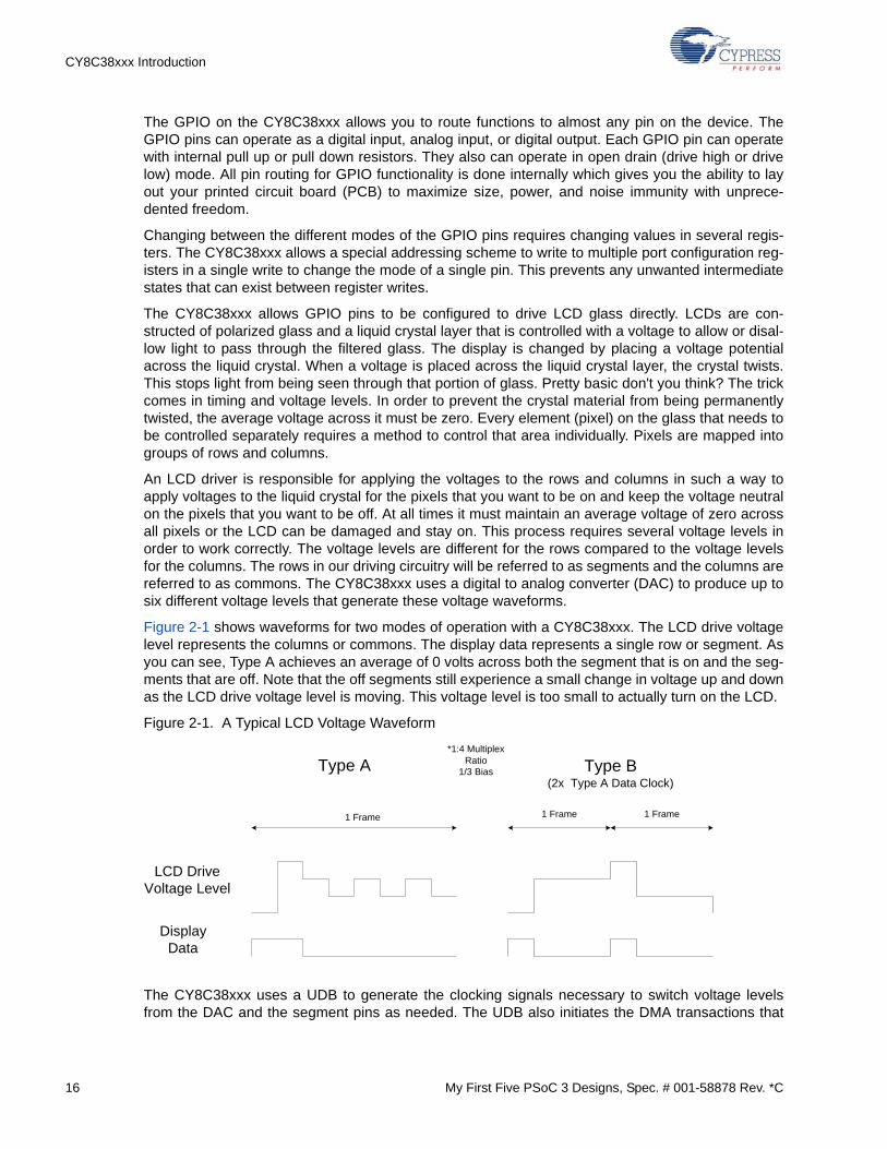
The CY8C38xxx allows GPIO pins to be configured to drive LCD glass directly. LCDs are con-structed of polarized glass and a liquid crystal layer that is controlled with a voltage to allow or disal-low light to pass through the filtered glass. The display is changed by placing a voltage potentialacross the liquid crystal. When a voltage is placed across the liquid crystal layer, the crystal twists.This stops light from being seen through that portion of glass. Pretty basic don't you think? The trickcomes in timing and voltage levels. In order to prevent the crystal material from being permanentlytwisted, the average voltage across it must be zero. Every element (pixel) on the glass that needs tobe controlled separately requires a method to control that area individually. Pixels are mapped intogroups of rows and columns.
An LCD driver is responsible for applying the voltages to the rows and columns in such a way toapply voltages to the liquid crystal for the pixels that you want to be on and keep the voltage neutralon the pixels that you want to be off. At all times it must maintain an average voltage of zero acrossall pixels or the LCD can be damaged and stay on. This process requires several voltage levels inorder to work correctly. The voltage levels are different for the rows compared to the voltage levelsfor the columns. The rows in our driving circuitry will be referred to as segments and the columns arereferred to as commons. The CY8C38xxx uses a digital to analog converter (DAC) to produce up tosix different voltage levels that generate these voltage waveforms.
Figure 2-1 shows waveforms for two modes of operation with a CY8C38xxx. The LCD drive voltagelevel represents the columns or commons. The display data represents a single row or segment. Asyou can see, Type A achieves an average of 0 volts across both the segment that is on and the seg-ments that are off. Note that the off segments still experience a small change in voltage up and downas the LCD drive voltage level is moving. This voltage level is too small to actually turn on the LCD.
Figure 2-1. A Typical LCD Voltage Waveform
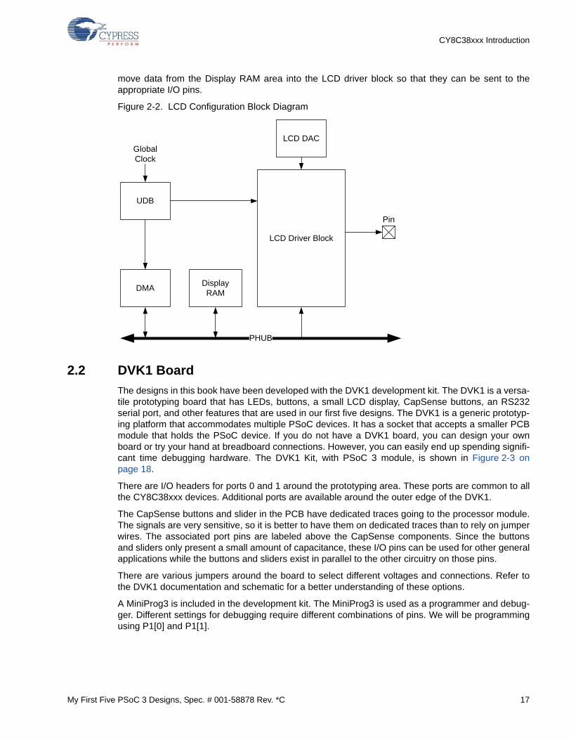
The CY8C38xxx uses a UDB to generate the clocking signals necessary to switch voltage levelsfrom the DAC and the segment pins as needed. The UDB also initiates the DMA transactions that
LCD Drive Voltage Level
DisplayData
Type A
1 Frame
*1:4 Multiplex Ratio
1/3 Bias
1 Frame
Type B(2x Type A Data Clock)
1 Frame
My First Five PSoC 3 Designs, Spec. # 001-58878 Rev. *C 17
CY8C38xxx Introduction
move data from the Display RAM area into the LCD driver block so that they can be sent to theappropriate I/O pins.
Figure 2-2. LCD Configuration Block Diagram
2.2 DVK1 Board
The designs in this book have been developed with the DVK1 development kit. The DVK1 is a versa-tile prototyping board that has LEDs, buttons, a small LCD display, CapSense buttons, an RS232serial port, and other features that are used in our first five designs. The DVK1 is a generic prototyp-ing platform that accommodates multiple PSoC devices. It has a socket that accepts a smaller PCBmodule that holds the PSoC device. If you do not have a DVK1 board, you can design your ownboard or try your hand at breadboard connections. However, you can easily end up spending signifi-cant time debugging hardware. The DVK1 Kit, with PSoC 3 module, is shown in Figure 2-3 onpage 18.
There are I/O headers for ports 0 and 1 around the prototyping area. These ports are common to allthe CY8C38xxx devices. Additional ports are available around the outer edge of the DVK1.
The CapSense buttons and slider in the PCB have dedicated traces going to the processor module.The signals are very sensitive, so it is better to have them on dedicated traces than to rely on jumperwires. The associated port pins are labeled above the CapSense components. Since the buttonsand sliders only present a small amount of capacitance, these I/O pins can be used for other generalapplications while the buttons and sliders exist in parallel to the other circuitry on those pins.
There are various jumpers around the board to select different voltages and connections. Refer tothe DVK1 documentation and schematic for a better understanding of these options.
A MiniProg3 is included in the development kit. The MiniProg3 is used as a programmer and debug-ger. Different settings for debugging require different combinations of pins. We will be programmingusing P1[0] and P1[1].
UDB
DMADisplay RAM
LCD Driver Block
LCD DAC
PHUB
GlobalClock
Pin

18 My First Five PSoC 3 Designs, Spec. # 001-58878 Rev. *C
CY8C38xxx Introduction
Figure 2-3. DVK1 Development Kit
2.3 PSoC Creator™
PSoC Creator is the complete design tool for the CY8C38xxx that allows you to configure the analogand digital resources within the device. It provides a code editor to write the firmware for your projectand links to your favorite compiler. PSoC Creator also provides programming and powerful debug-ging tools to finalize your design.
PSoC Creator displays much of its information in web page format. It is highly integrated to the Inter-net and can automatically retrieve additional help and design examples from the Internet for youruse. When you first invoke the program, PSoC Creator opens to the start page. The start pageallows you to open recent projects, start new projects, check for updates, and build projects basedfrom reference designs on the Cypress website. PSoC Creator scans your system for developmentkits that you have purchased and connected to the computer to customize this view to the hardwarethat you have available. The start page also includes links to tutorials, help files, and externalsources of help such as application notes and forums.
There are three basic areas of design for each PSoC project.
■ First, you need to configure system-wide resources, such as clocking, voltage levels, analog ref-erences, and so on.

My First Five PSoC 3 Designs, Spec. # 001-58878 Rev. *C 19
CY8C38xxx Introduction
■ Second, you need to configure the fixed function and configurable analog and digital resources within the PSoC.
■ Third, you need to write the firmware associated with your project.
PSoC Creator helps you complete these three steps. The process is very simple and will becomesecond nature to you very quickly. Changes can be made to the design at any time to any of thethree areas. When you generate and compile the project, PSoC Creator will integrate the latestchanges into the completed output file. Navigation through the different areas of your design is madevery simple with Workspace Explorer.
2.3.1 Workspace Explorer
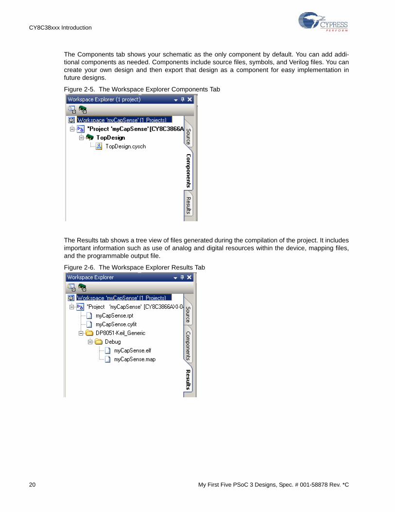
Workspace Explorer is a dockable window that allows quick access to any part of your design. Likethe other dockable windows within PSoC Creator, Workspace Explorer can be docked in variouspositions around the PSoC Creator window. Workspace Explorer also offers an autohide feature thatcan be toggled on and off by clicking on the push pin icon in the top right of the window. The auto-hide feature hides Workspace Explorer and leaves a small tab. When you mouse over the small tab,Workspace Explorer reappears. Each workspace can contain one or more projects. WorkspaceExplorer divides the files of each project into three tabs: Source, Components, and Results.
The Source tab shows a tree view of the source and header files that are included in your project.Double clicking on a file opens that file as a new tab within PSoC Creator for editing. Right clickingthe file allows you to compile that file or change the build settings for that file. The Source tab alsoallows you to open the ProjectName.cydwr (Cypress design wide resources) file and the Top Sche-matic file.
Figure 2-4. The Workspace Explorer Source Tab
20 My First Five PSoC 3 Designs, Spec. # 001-58878 Rev. *C
CY8C38xxx Introduction
The Components tab shows your schematic as the only component by default. You can add addi-tional components as needed. Components include source files, symbols, and Verilog files. You cancreate your own design and then export that design as a component for easy implementation infuture designs.
Figure 2-5. The Workspace Explorer Components Tab
The Results tab shows a tree view of files generated during the compilation of the project. It includesimportant information such as use of analog and digital resources within the device, mapping files,and the programmable output file.
Figure 2-6. The Workspace Explorer Results Tab

My First Five PSoC 3 Designs, Spec. # 001-58878 Rev. *C 21
CY8C38xxx Introduction
2.3.2 Design-Wide Resources
Design-wide resources include clocking signals, interrupts, DMA, and I/O pins. Access the design-wide resources by double clicking the .cydwr file in the Workspace Explorer. Opening this file allowsyou to configure those global resources for the device. Note that you must add appropriate compo-nents to the schematic view before they can be configured in design-wide resources.
Figure 2-7. Design-Wide Resources
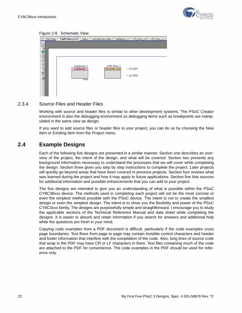
2.3.3 Schematic View
Schematic view is the visual depiction of what components have been selected within a project andhow they are connected. Access the schematic view by double clicking the .cysch file in the Work-space Explorer. Drawing the components in a schematic fashion gives a very intuitive view of howthe device is configured. Schematic view allows you to type notes and draw figures next to yourcomponents to help describe the design and its purposes. For more complex designs, you can havemultiple sheets of schematics that describe a single design. Tags allow the connection of compo-nents between different sheets.
PSoC Creator will configure chip resources to match what you have selected and connected withinschematic view.
22 My First Five PSoC 3 Designs, Spec. # 001-58878 Rev. *C
CY8C38xxx Introduction
Figure 2-8. Schematic View
2.3.4 Source Files and Header Files
Working with source and header files is similar to other development systems. The PSoC Creatorenvironment is also the debugging environment so debugging items such as breakpoints are manip-ulated in the same view as design.
If you want to add source files or header files to your project, you can do so by choosing the NewItem or Existing Item from the Project menu.
2.4 Example Designs
Each of the following five designs are presented in a similar manner. Section one describes an over-view of the project, the intent of the design, and what will be covered. Section two presents anybackground information necessary to understand the processes that we will cover while completingthe design. Section three gives you step by step instructions to complete the project. Later projectswill quickly go beyond areas that have been covered in previous projects. Section four reviews whatwas learned during the project and how it may apply to future applications. Section five lists sourcesfor additional information and possible enhancements that you can add to your project.
The five designs are intended to give you an understanding of what is possible within the PSoCCY8C38xxx device. The methods used in completing each project will not be the most concise oreven the simplest method possible with the PSoC device. The intent is not to create the smallestdesign or even the simplest design. The intent is to show you the flexibility and power of the PSoCCY8C3xxx family. The designs are purposefully simple and straightforward. I encourage you to studythe applicable sections of the Technical Reference Manual and data sheet while completing thedesigns. It is easier to absorb and retain information if you search for answers and additional helpwhile the questions are fresh in your mind.
Copying code examples from a PDF document is difficult, particularly if the code examples crosspage boundaries. Text flows from page to page may contain invisible control characters and headerand footer information that interfere with the compilation of the code. Also, long lines of source codethat wrap in the PDF may have CR or LF characters in them. Text files containing much of the codeare attached to the PDF for convenience. The code examples in the PDF should be used for refer-ence only.

My First Five PSoC 3 Designs, Spec. # 001-58878 Rev. *C 23
3. Learn By Example: Blink an LED
3.1 Project Overview
This chapter demonstrates how to build a basic project. The project covers three important areas:input, output, and timing. Tactile buttons are used to change the method of blinking the LED. Thepurpose of the task is not to simply blink an LED, but to build a basic timing structure for more com-plex projects.
The project sets up an 8-bit PWM and generates an interrupt on the terminal count of that PWM.Software counters and flags within the interrupt routine establish a flexible time base for blinking theLED and other future tasks.
Each project in this book will build on the resources of the previous projects. It is necessary to com-plete each chapter in turn in order to have all the resources needed for later chapters. This chapterdescribes a more in-depth step by step process of building a project than subsequent chapters.
3.2 Background Information
Blinking an LED is a common first step with any project that uses a new microcontroller or all newhardware. It allows you to accomplish a simple straightforward task that generally does not requireany special equipment beyond the programmer and development software (assuming that the hard-ware does not have a problem). Since blinking an LED is a simple project, it is easy to debug andtest. It can also be a powerful tool to debug other parts of hardware on your project. There havebeen many times when I have written code for a complex project before hardware was available forthat project. There have also been many times when I have programmed my first code onto thesenew projects, flipped the power switch, and had nothing happen at all. If the problem cannot befound easily, then I will revert back to blinking an LED to give me a foundation to test the rest of theproject.
Task management is a basic part of any embedded design. Different systems manage tasks in differ-ent ways. This project executes tasks in a periodic fashion. We will create a timing system thatallows tasks to complete every 0.001 seconds, every 0.1 seconds, and every 1.0 seconds. The tim-ing system consists of a timer that reaches its terminal count and trips an interrupt every 0.001 sec-onds. Software counters are used to derive the other periods from the millisecond period. We willuse flags to signal to the project main loop that a particular interval has passed.
The method of using flags to signal that an event has happened will let us use that flag elsewhere todetermine when a task should run. If we try to execute the entire task within the interrupt rather thansetting a flag and running the task outside of the interrupt, we will need to limit the task executiontime to the constraints of the timing interrupt. If we try to perform too large a task in an interrupt, wecan experience interrupt overflow and subsequent timing problems.
24 My First Five PSoC 3 Designs, Spec. # 001-58878 Rev. *C
Learn By Example: Blink an LED
3.3 Project Steps
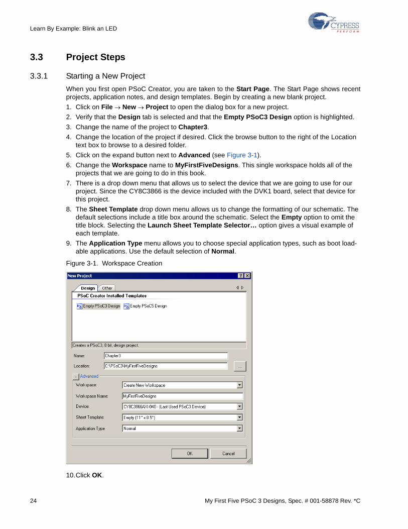
3.3.1 Starting a New Project
When you first open PSoC Creator, you are taken to the Start Page. The Start Page shows recentprojects, application notes, and design templates. Begin by creating a new blank project.
1. Click on File New Project to open the dialog box for a new project.
2. Verify that the Design tab is selected and that the Empty PSoC3 Design option is highlighted.
3. Change the name of the project to Chapter3.
4. Change the location of the project if desired. Click the browse button to the right of the Location text box to browse to a desired folder.
5. Click on the expand button next to Advanced (see Figure 3-1).
6. Change the Workspace name to MyFirstFiveDesigns. This single workspace holds all of the projects that we are going to do in this book.
7. There is a drop down menu that allows us to select the device that we are going to use for our project. Since the CY8C3866 is the device included with the DVK1 board, select that device for this project.
8. The Sheet Template drop down menu allows us to change the formatting of our schematic. The default selections include a title box around the schematic. Select the Empty option to omit the title block. Selecting the Launch Sheet Template Selector… option gives a visual example of each template.
9. The Application Type menu allows you to choose special application types, such as boot load-able applications. Use the default selection of Normal.
Figure 3-1. Workspace Creation
10.Click OK.

My First Five PSoC 3 Designs, Spec. # 001-58878 Rev. *C 25
Learn By Example: Blink an LED
PSoC Creator generates the associated directories and files needed for your project and opens intoschematic view (see Figure 3-2). Schematic view gives the overall picture of the components youhave selected for your project and how they are connected to other components. You should seeWorkspace Explorer to the left of your schematic, the Component Catalog to the right of yourschematic, and the Output window below your schematic. If you do not see all three of these win-dows, click the View menu and choose the missing window from the menu.
Figure 3-2. Schematic View
3.3.2 Adding Components
This project is very simple so you only need a few components.
3.3.2.1 Adding a Clock Component
1. Locate the Clock component under the System group in the Component Catalog. The Compo-nent Catalog is found to the right of your blank schematic sheet.
2. Drag the Clock component from the Component Catalog onto the schematic. Controls to zoom in on your components within the schematic are found under the View menu and in the tool bar at the top of schematic view.
3. Right click on the Clock component and select Configure from the context menu. The Config-ure dialog allows you to set up default properties for that component. The Configure dialog can also be opened for a component by simply double clicking the component.
4. Change the Name of the clock component to clock_PWM (Figure 3-3 on page 26). Pay close attention to the case of names of the components. The name that you select for each component is used when the project is built to generate names for the associated application programmer’s interface (API) calls. The provided code will not work correctly if the names do not match exactly.
5. Change the Desired Frequency to 100 kHz.
6. Click OK to close the Configure dialog.

26 My First Five PSoC 3 Designs, Spec. # 001-58878 Rev. *C
Learn By Example: Blink an LED
Figure 3-3. clock_PWM Configuration
The Data Sheet button in the Configure dialog opens the data sheet associated with that compo-nent. The data sheet for any component can also be easily opened by right clicking on the compo-nent in schematic view and selecting the data sheet from the menu. The data sheet describes thefunctionality of the component including available connections and parameters of the component.The data sheet also includes example source code for that component.
3.3.2.2 Adding a PWM Component
1. Locate the PWM component under the Digital Functions section of the Component Catalog.
2. Click the PWM component and drag it onto your blank schematic sheet.
The PWM will be used for a dual purpose in our project. It allows us to create a quick signal that will show that the PWM component is up and running and also allows us to interrupt on the termi-nal count of the PWM to create a timing base.
PSoC 3 and 5 have up to four basic fixed-function counter/timer/PWM blocks. If your application is simple then the fixed-function blocks can be used instead of UDB-based components, saving UDB resources. For this project either one will work, and we will simply stay with the default which is UDB-based.
3. Drag the clock_PWM component so that it connects with the clock input of the PWM compo-nent. The small boxes at the end of the connection points should disappear when connected properly (See Figure 3-4).
My First Five PSoC 3 Designs, Spec. # 001-58878 Rev. *C 27
Learn By Example: Blink an LED
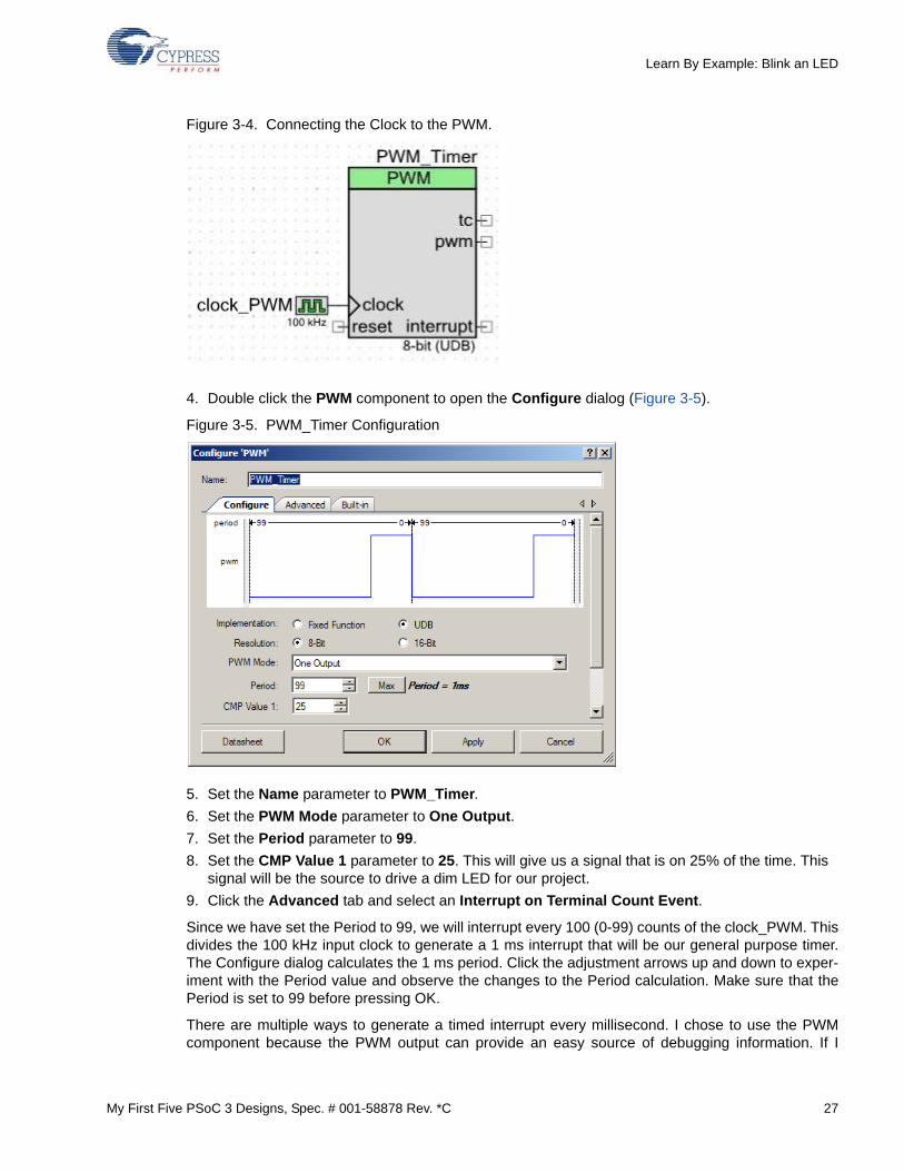
Figure 3-4. Connecting the Clock to the PWM.
4. Double click the PWM component to open the Configure dialog (Figure 3-5).
Figure 3-5. PWM_Timer Configuration
5. Set the Name parameter to PWM_Timer.
6. Set the PWM Mode parameter to One Output.
7. Set the Period parameter to 99.
8. Set the CMP Value 1 parameter to 25. This will give us a signal that is on 25% of the time. This signal will be the source to drive a dim LED for our project.
9. Click the Advanced tab and select an Interrupt on Terminal Count Event.
Since we have set the Period to 99, we will interrupt every 100 (0-99) counts of the clock_PWM. Thisdivides the 100 kHz input clock to generate a 1 ms interrupt that will be our general purpose timer.The Configure dialog calculates the 1 ms period. Click the adjustment arrows up and down to exper-iment with the Period value and observe the changes to the Period calculation. Make sure that thePeriod is set to 99 before pressing OK.
There are multiple ways to generate a timed interrupt every millisecond. I chose to use the PWMcomponent because the PWM output can provide an easy source of debugging information. If I
28 My First Five PSoC 3 Designs, Spec. # 001-58878 Rev. *C
Learn By Example: Blink an LED
wanted to observe a internal register value in real time operation, I can copy that value to the CMPregister. If I have a simple LED connected to this register, I can get a rough estimation of the value ofthe register by observing the brightness of the LED. If I have an oscilloscope or a good meter withthe ability to measure a duty cycle, then I can get a more exact value of the register value. If I con-struct a simple low pass filter with a resistor and capacitor connected to the PWM output then I canget a good estimation of the register value with a simple voltage measurement.
3.3.2.3 Adding a Digital Pin Component
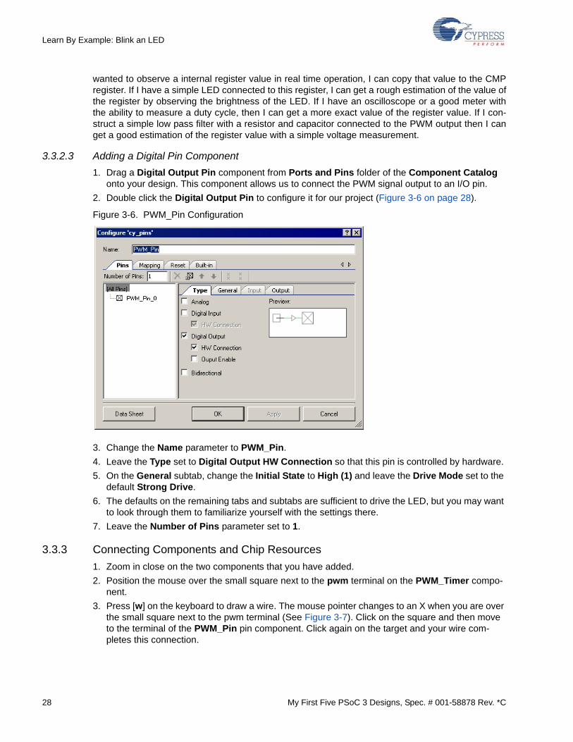
1. Drag a Digital Output Pin component from Ports and Pins folder of the Component Catalog onto your design. This component allows us to connect the PWM signal output to an I/O pin.
2. Double click the Digital Output Pin to configure it for our project (Figure 3-6 on page 28).
Figure 3-6. PWM_Pin Configuration
3. Change the Name parameter to PWM_Pin.
4. Leave the Type set to Digital Output HW Connection so that this pin is controlled by hardware.
5. On the General subtab, change the Initial State to High (1) and leave the Drive Mode set to the default Strong Drive.
6. The defaults on the remaining tabs and subtabs are sufficient to drive the LED, but you may want to look through them to familiarize yourself with the settings there.
7. Leave the Number of Pins parameter set to 1.
3.3.3 Connecting Components and Chip Resources
1. Zoom in close on the two components that you have added.
2. Position the mouse over the small square next to the pwm terminal on the PWM_Timer compo-nent.
3. Press [w] on the keyboard to draw a wire. The mouse pointer changes to an X when you are over the small square next to the pwm terminal (See Figure 3-7). Click on the square and then move to the terminal of the PWM_Pin pin component. Click again on the target and your wire com-pletes this connection.
My First Five PSoC 3 Designs, Spec. # 001-58878 Rev. *C 29
Learn By Example: Blink an LED
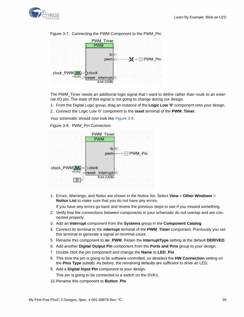
Figure 3-7. Connecting the PWM Component to the PWM_Pin
The PWM_Timer needs an additional logic signal that I want to define rather than route to an exter-nal I/O pin. The state of this signal is not going to change during our design.
1. From the Digital Logic group, drag an instance of the Logic Low ‘0’ component onto your design.
2. Connect the Logic Low ‘0’ component to the reset terminal of the PWM_Timer.
Your schematic should now look like Figure 3-8.
Figure 3-8. PWM_Pin Connection
1. Errors, Warnings, and Notes are shown in the Notice list. Select View > Other Windows > Notice List to make sure that you do not have any errors.
If you have any errors go back and review the previous steps to see if you missed something.
2. Verify that the connections between components in your schematic do not overlap and are con-nected properly.
3. Add an Interrupt component from the Systems group in the Component Catalog.
4. Connect its terminal to the interrupt terminal of the PWM_Timer component. Previously you set this terminal to generate a signal on terminal count.
5. Rename this component to isr_PWM. Retain the InterruptType setting at the default DERIVED.
6. Add another Digital Output Pin component from the Ports and Pins group to your design.
7. Double click the pin component and change the Name to LED_Pin.
8. This time the pin is going to be software controlled, so deselect the HW Connection setting on the Pins Type subtab. As before, the remaining defaults are sufficient to drive an LED.
9. Add a Digital Input Pin component to your design.
This pin is going to be connected to a switch on the DVK1.
10.Rename this component to Button_Pin.

30 My First Five PSoC 3 Designs, Spec. # 001-58878 Rev. *C
Learn By Example: Blink an LED
11.On the General subtab of the Pins tab change the Drive Mode to Resistive Pull Up.
12.Set the Initial State to High (1). When you press the button, the pin is grounded and the state goes low.
Your schematic should now look like Figure 3-9 on page 30.
Figure 3-9. Chapter3 Schematic
3.3.4 Assigning Pins
Before you build the project, you must tell PSoC Creator which pins to use for each of these signals.PSoC Creator will optimize the routing of internal logic and muxes to minimize resources. When youare first creating a project, place all the components and connections and examine the routing PSoCCreator chooses before you create your PCB. Inefficient routing can quickly consume resources andmay even lead to a situation where you do not have enough resources to successfully complete theneeded routing. If you have the flexibility to let PSoC Creator route the signals and then match yourboard to that routing, you will be able to benefit from this optimization.
Since our PCB is already defined, we will need to force PSoC Creator to route the pins to match theconnections available on the DVK1 board. You will also need to connect wires from the headers tothe right of the prototyping area to complete the circuit between the I/O pins and LEDs, buttons, etc.
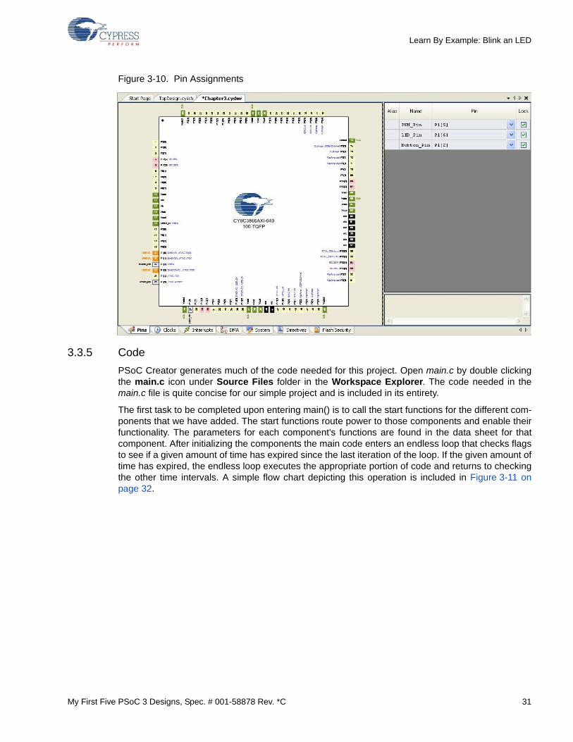
1. Double click on the Chapter3.cydwr (Cypress design-wide resources) file from the Workspace Explorer.
2. Select the Pins tab at the bottom to show the pin configuration of the project. You will see a graphic of the CY8C3866 PSoC with a description of the I/O pins and routing results.
3. Select P1[5] for the PMW_Pin, P1[6] for the LED_Pin, and P1[2] for the Button_Pin.
4. From the Build menu, select Build Chapter 3 and verify that you do not have any errors (Figure 3-10 on page 31).
My First Five PSoC 3 Designs, Spec. # 001-58878 Rev. *C 31
Learn By Example: Blink an LED
Figure 3-10. Pin Assignments
3.3.5 Code
PSoC Creator generates much of the code needed for this project. Open main.c by double clickingthe main.c icon under Source Files folder in the Workspace Explorer. The code needed in themain.c file is quite concise for our simple project and is included in its entirety.
The first task to be completed upon entering main() is to call the start functions for the different com-ponents that we have added. The start functions route power to those components and enable theirfunctionality. The parameters for each component's functions are found in the data sheet for thatcomponent. After initializing the components the main code enters an endless loop that checks flagsto see if a given amount of time has expired since the last iteration of the loop. If the given amount oftime has expired, the endless loop executes the appropriate portion of code and returns to checkingthe other time intervals. A simple flow chart depicting this operation is included in Figure 3-11 onpage 32.

32 My First Five PSoC 3 Designs, Spec. # 001-58878 Rev. *C
Learn By Example: Blink an LED
Figure 3-11. Main Routine Flow Chart
#include <device.h>#include "timing.h"
void ToggleLed(void);
/******************************************************************************** Function Name: main()********************************************************************************* Summary:* Contains initialization for different components and main loop** Parameters:* none** Return:* none******************************************************************************/void main(){ /* Components should be initialized in the following order:
* 1. interrupts* 2. sources of interrupts (clocks are auto-initialized)* 3. global interrupt enable*/
Main() Entry
Initialization of Components
Has 1 ms passed?
Execute code for this interval
Has 0.1 s passed?
Execute code for this interval
Has 1 s passed?
Execute code for this interval

My First Five PSoC 3 Designs, Spec. # 001-58878 Rev. *C 33
Learn By Example: Blink an LED
InitTiming(); /* interrupt */ PWM_Timer_Start(); /* source of interrupt */ CYGlobalIntEnable /* macro */
for(;;) /* main loop - do forever */ {
/* This section contains code to be executed every millisecond */ if(milliSecond) { milliSecond = 0U; } /* end of millisecond section */
/* This section contains code to be executed every tenth second */ if(tenthSecond) { tenthSecond = 0U;
/* Toggle the LED if the button is NOT pressed. This will cause * the LED to blink rapidly when the button is NOT pressed. */ if(Button_Pin_Read()) /* read a 1 when button is NOT pressed */ { ToggleLed(); } } /* end of tenth second section */
/* This section contains code to be executed every second */ if(oneSecond) { oneSecond = 0U;
/* Toggle the LED if the button IS pressed. This will cause * the LED to blink slowly when the button IS pressed. */ if(!Button_Pin_Read()) /* read a 0 when button IS pressed */ { ToggleLed(); } } /* end of one second section */ } /* end of do forever loop */} /* end of main */
/******************************************************************************** Function Name: ToggleLed()********************************************************************************* Summary:* Toggles the LED** Parameters:* none** Return:* none*******************************************************************************/void ToggleLed(void){ /* Set the pin to the opposite of what is read from the pin. The pin value
34 My First Five PSoC 3 Designs, Spec. # 001-58878 Rev. *C
Learn By Example: Blink an LED
* is always right-justified to the LS bits.*/
LED_Pin_Write(LED_Pin_Read() ^ 1U);} /* end of ToggleLed */
In the initialization area of main(), first enable the interrupt by calling InitTiming(). The clock compo-nent, Clock_PWM, is automatically enabled. To confirm this you can look at the Clocks tab of the.cydwr file. There is a check in the Start on Reset column. Then call the enable function for thesource of the interrupt, the PWM_Timer component. After starting the PWM_Timer and isr_PWMcomponents, you enable the global interrupt flag so that the isr_PWM component can be servicedwhen the terminal count of the PWM_Timer is reached.
The SW1 button on the DVK1 board will short the SW1 pin to ground when pressed. When youcheck the status of the button with Button_Pin_Read() the result will be 0 (or ‘false’) when thebutton is pressed, and 1 when it is not. For this reason, (!(Button_Pin_Read()) is true whenthe button is pressed.
The final function in main.c file is the toggleLED function. The toggleLED function simply toggles thestate of the appropriate bit in the data register to change the state of the LED_Pin.
One important piece of information to note here is that I am getting the state of the DataReg (dataregister) and I am toggling that value before writing it back to the data register. This is the value thatis written to the output latches of the I/O logic. The alternative value you can examine is the valueread from the state of the pin using the PS (pin state) register. An example of reading the PS registerinstead of the data register is given here.
CY_SET_REG8(LED_Pin__DR,(CY_GET_REG8(LED_Pin__PS)^LED_Pin__MASK));
I do not recommend using the PS register when you toggle an output because if the pin on that reg-ister does not currently see the same logic as the DR register, then an incorrect value will be writtenback to the DR register. Consider our button component as an example. We have output a high tothe button DR register bit to enable the pull up resistor. However, when SW1 is depressed, the PSregister bit will be a zero. If we were to toggle another bit on that same port using the PS registerinstead of the DR register, then we would write a zero to that register. This results in the pull up beingdisabled. The project will interpret the SW1 button being pressed even when it is not pressed.
1. Add a file to your project called timing.c.
2. Highlight the Project 'Chapter3'[CY8C3866AXI-40] icon in the Workspace Explorer and right click on it.
3. Add a New Item from the context menu.
4. Select C File from the list of templates and change the name to timing.c.
5. Pressing OK creates the timing.c file, adds it to the project, and opens that file for editing. Copy the code below into the timing.c file.
#include <device.h>#include "timing.h"
/**************************************** Global Variables***************************************//* event flags for each of the time periods */uint8 milliSecond;uint8 tenthSecond;uint8 oneSecond;

My First Five PSoC 3 Designs, Spec. # 001-58878 Rev. *C 35
Learn By Example: Blink an LED
/**************************************** Private Functions***************************************//****************************************************************************** Function Name: TimerIsr()******************************************************************************* Summary:* An Interrupt Service Routine (ISR) for the pulse width modulator. This* function is not public. The ISR provides basic timing for all background* functions. It is assumed that the ISR is called once per millisecond.** Parameters:* none** Return:* None. Timing event flags are set.******************************************************************************/static CY_ISR(TimerIsr){ /* counters for the longer time periods */
static uint8 tenthSecondCount = 0U;static uint8 oneSecondCount = 0U;
/* Read the PWM status byte to clear the interrupt source. Since function* calls should not be done from interrupt handlers, the register is read* directly. Dump the value into a dummy location; we're not interested in* the value of the register.*/(void)PWM_Timer_STATUS;
milliSecond = 1U; /* always set the millisecond global event flag */
/* see if a tenth second has passed */ tenthSecondCount++; if(tenthSecondCount > 99U) { tenthSecondCount = 0U; tenthSecond = 1U; /* tenth second global event flag */
/* see if one second has passed */oneSecondCount++;
if(oneSecondCount > 9U) { oneSecondCount = 0U; oneSecond = 1U; /* one second global event flag */ } }} /* end of TimerIsr() */
/**************************************** Global Functions***************************************//****************************************************************************** Function Name: InitTiming()*****************************************************************************/void InitTiming(void)

36 My First Five PSoC 3 Designs, Spec. # 001-58878 Rev. *C
Learn By Example: Blink an LED
{ isr_PWM_Start();
/* set the interrupt's ISR function to be the one in this file */isr_PWM_SetVector(TimerIsr);
} /* end of InitTiming() */
/******************************************************************************** Function Name: TenthSecondDelay()*******************************************************************************/void TenthSecondDelay(uint8 count){ /* count down every tenth second, and return when counted down to zero */ do { while(!tenthSecond){} tenthSecond = 0U; count--; } while(count != 0U);}/* end of TenthSecondDelay() */
1. Right click on the Project icon in Workspace Explorer and Add a New Item.
2. This time select a Header File from the list of templates and name the header file timing.h.
3. Add the following code to the timing.h file.
/**************************************** Function Prototypes***************************************//****************************************************************************** Function Name: InitTiming()******************************************************************************* Summary:* Initializes the timing system, particularly the interrupt component and* the ISR.** Parameters:* none** Return:* none******************************************************************************/void InitTiming(void);
/******************************************************************************** Function Name: TenthSecondDelay()********************************************************************************* Summary:* Waits for a given delay in tenths of seconds. The actual delay will be:* count - 1 < actual delay ? count** Parameters:* uint8 number of tenth-seconds to wait** Return:* none*******************************************************************************/

My First Five PSoC 3 Designs, Spec. # 001-58878 Rev. *C 37
Learn By Example: Blink an LED
void TenthSecondDelay(uint8 count);
/**************************************** Global Variables***************************************//* These timing event flags are set at the corresponding time interval by the ISR.* It is the responsibility of the background function to reset them before they* are set again.*/extern uint8 milliSecond;extern uint8 tenthSecond;extern uint8 oneSecond;
An interrupt service routine for the isr_PWM component exists in the isr_PWM.c file generated by PSoC Creator. However, we will be using our own interrupt service routine, TimerIsr(), defined in timing.c. Note the 'CY_ISR' macro that defines that this function is an interrupt service routine. In the InitTiming() function, after we initialize the interrupt by calling isr_PWM_Start(), we change the interrupt's vector to point to our routine by calling isr_PWM_SetVector().
3.3.6B: Building and Debugging Your Project
1. Build the project and verify that there are no errors in your project.
2. On the DVK1 development board, connect a wire from P1_5 to the top of LED1.
3. Connect a wire from P1_6 to the top of LED2.
4. Connect a third wire from P1_2 to SW1 (Figure 3-12). SW1 is a momentary, normally open button that will short the signal to ground when pressed. We have configured our button component to supply an internal pull up resistor for SW1.
Figure 3-12. Wire Connections
5. Select Execute Code from the Debug menu of PSoC Creator.
6. Alternatively, you can press [F5] or click on the small bug icon from the Build/Debug toolbar.

38 My First Five PSoC 3 Designs, Spec. # 001-58878 Rev. *C
Learn By Example: Blink an LED
Executing code will build the project if any changes have been made to source files or any config-uration. It will program the target device and will halt at the main label in main.c.
7. Press the small green arrow on the Debugger toolbar or press [F5] to continue executing code.
You should see a dim light coming from LED1, and LED2 should be flashing at 5 Hz. Pressing onSW1 should change the blink rate of LED2 to 0.5 Hz.
3.4 Conclusions
This project demonstrated one of many ways to create a periodic interrupt. The method used in thisproject allows you to configure system-wide resources, digital logic in the UDB blocks, and I/O pins.The PWM module created a system that is easy to debug at the most rudimentary levels so that youhave a basis for the other projects in this book. If a project from the other chapters is not working cor-rectly, make sure that this basic LED functionality is still working. If it is not working correctly, thenmake sure to restore that functionality first as it is a requirement for the added features of the otherprojects.
The timing flags create a basic task scheduler that can be easily altered to meet different periodicrequirements. The use of timing flags set within a timing interrupt allows the bulk of code executionto be done outside the interrupt. If execution of a task is very time critical and needs to be able tointerrupt other task execution, that task can be called from within the timing interrupt. Caution shouldbe taken to make sure that any task execution called from within the timing interrupt does not takelonger to execute than the period of the timing interrupt.
3.5 Additional Information
It is easy to use a single LED to show many different states. The best method depends on your par-ticular project. I suggest at least two simple methods. The first is to have a continual repeating blinkof a specific period. The current state is defined by the period of the LED. In the example codebelow, I have created a blinking LED that is controlled by the routine stateBlink. I have changed thePin component name to be LED_Pin2 so that you can add it as a separate component and add thiscode to the example above without additional changes. This routine is called every 0.1 seconds andwill give a quick flash of the LED for 0.1 seconds followed by an interval of 0.1 seconds times thevalue of state. A state value of zero (0) is indicated by a LED is that always on. A state value of oneshows a blinking LED at a rate of five Hz. A state of nine blinks at one Hz.
/******************************************************************************** Function Name: stateBlink********************************************************************************* Summary:* Blinks a specific amount of blinks** Parameters:* none** Return:* none******************************************************************************/
/* state value used for real time debugging */unsigned char state;
/* Counter for state value blinking */unsigned char blinkCount;

My First Five PSoC 3 Designs, Spec. # 001-58878 Rev. *C 39
Learn By Example: Blink an LED
void stateBlink(void){ /* Check to see if blinkCount has reached zero yet */ if(blinkCount>0) { /* If it is not zero, then default the LED off */ LED_Pin2_Write(0); /* Update the counter */ blinkCount--; } /* Come here if blink Count was already zero */ else { /* Set this one for one count */ LED_Pin2_Write(1); /* Initialize the down counter */ blinkCount=state; }}
The second recommended method for displaying a state is to use a counter so that the LED isblinked the amount of times equal to the value of state.
/******************************************************************************** Function Name: stateBlinkDecode********************************************************************************* Summary:* Blinks a specific amount of blinks** Parameters:* none** Return:* none******************************************************************************/
/* Constant used in the Additional Information section */#define BLANKTIME 10
/* Counter for state value blinking */unsigned char blinkCount1;
void stateBlinkDecode(void){ if(blinkCount1>0) { /* Decrement blinkCounter */ blinkCount1--; if((blinkCount1>BLANKTIME)&(blinkCount1%2)) { /* Turn on the LED; */ LED_Pin3_Write(1);

40 My First Five PSoC 3 Designs, Spec. # 001-58878 Rev. *C
Learn By Example: Blink an LED
} else { /* Turn off the LED; */ LED_Pin3_Write(0); } } else { /* Turn off the LED; */ LED_Pin3_Write(0); /* set up for the next round of blinking */ blinkCount1=(state*2)+BLANKTIME; }}
This method is simple and straightforward. It becomes more cumbersome as the numbers becomelarger. A suggestion for larger numbers is to break the number up into digits. For example, a code of35 could be shown by a set of three blinks of the LED, a short pause and then a set of five blinks ofthe LED. This could be done digitally in the UDBs so that blinking LEDs would not burden the CPU.

My First Five PSoC 3 Designs, Spec. # 001-58878 Rev. *C 41
4. Learn By Example: UART
4.1 Project Overview
This chapter demonstrates how to configure a universal asynchronous receiver transmitter (UART)in the CY8C3866 and use a 2x16 LCD display. The UART provides a communication link betweenyour project and a computer. To complete this project you will need a computer with a fast COM portor a USB to RS232 converter. The LCD display is used to display some debugging information.
This project builds on the Chapter3 project. You need to have the Chapter3 project completed andrunning before beginning this project. If you want to hurry through the book, you can simply start withthe Chapter3 project and add additional components and code for this chapter to that same project. Irecommend starting over with a new project called Chapter4 and adding new components with thesame settings as you used in the Chapter3 project. Starting over with a new project helps you gainfamiliarity with PSoC Creator. You can have several projects within the same workspace. It is possi-ble to link components from different projects within PSoC Creator but that does create some inter-dependency considerations that are beyond the scope of this book.
4.2 Background Information
For decades the UART serial communications port has been a basic link to communicate betweenthe personal computer and external devices. The communication is basic, simple, needs little cir-cuitry, and requires only two data lines to transmit and receive. Transmission and reception of datacan happen simultaneously since the transmit and receive are on separate pins.
UART communication does not have a clock signal. Each bit is transmitted for a specific length oftime. The designation of bit time is given in the number of bits per second that can be transferred.This designation is also referred to as baud rate. The baud rate must be determined before commu-nication starts. Some systems implement algorithms to negotiate the current baud rate from a prede-termined list by testing a received string of communication at different speeds.
Each byte of communication is framed by a start bit and a stop bit. The start and stop bits are used toalign the data so it can be properly sampled. The UART does allow for some variation in the stop bitlength as well as how many data bits are transmitted at a time. This example uses the setting ofeight data bits and a stop bit length of one.
UARTs continue to be common peripherals in various embedded systems. Recently, the desktopand computer industry have been removing COM ports from their hardware in favor of USB. TheUSB interface is a more complex interface that is much more powerful in its abilities. It can easilyserve as a single transmit and receive datapath to mimic the serial communications port.
The PSoC device can create a USB to UART bridge for your project. The USB2UART componentwas not available at the time of publication, so this project will use a basic UART that connects to theRS232 voltage level translator on the DVK1 board.

42 My First Five PSoC 3 Designs, Spec. # 001-58878 Rev. *C
Learn By Example: UART
4.3 Project Steps
This project adds to the project from Chapter 3. To maintain independence in all five projects, I amrebuilding the components from Chapter 3 into a new project called Chapter4. It is a good practice toclose all the open windows before creating the other project so that you do not accidentally changethe wrong file.
4.3.1 Adding a New Project
1. Click File Add New Project to open the Add New Project dialog box.
2. Enter Chapter4 for the project name.
The Workspace Name is already set to MyFirstFiveDesigns (Figure 4-1). The new projectChapter4 will be saved in a separate directory under the MyFirstFiveDesigns folder.
Figure 4-1. Chapter4 Project Creation
The advantages of rebuilding each chapter from scratch include the ability to see all five projects inthe same session of PSoC Creator. You can also easily go back to a previous project with the assur-ance that the older project is not affected by changes made in the new project. You also gain confi-dence and speed in placing and configuring new components.
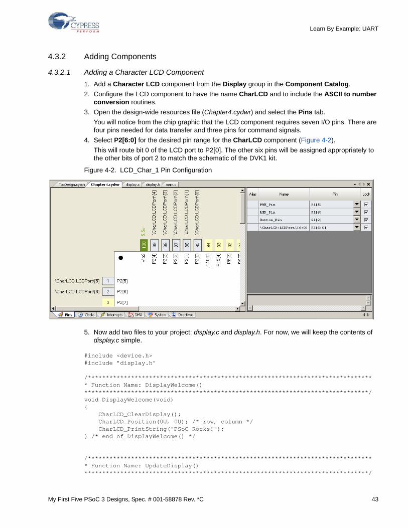
My First Five PSoC 3 Designs, Spec. # 001-58878 Rev. *C 43
Learn By Example: UART
4.3.2 Adding Components
4.3.2.1 Adding a Character LCD Component
1. Add a Character LCD component from the Display group in the Component Catalog.
2. Configure the LCD component to have the name CharLCD and to include the ASCII to number conversion routines.
3. Open the design-wide resources file (Chapter4.cydwr) and select the Pins tab.
You will notice from the chip graphic that the LCD component requires seven I/O pins. There are four pins needed for data transfer and three pins for command signals.
4. Select P2[6:0] for the desired pin range for the CharLCD component (Figure 4-2).
This will route bit 0 of the LCD port to P2[0]. The other six pins will be assigned appropriately to the other bits of port 2 to match the schematic of the DVK1 kit.
Figure 4-2. LCD_Char_1 Pin Configuration
5. Now add two files to your project: display.c and display.h. For now, we will keep the contents of display.c simple.
#include <device.h>#include "display.h"
/******************************************************************************** Function Name: DisplayWelcome()*******************************************************************************/void DisplayWelcome(void){ CharLCD_ClearDisplay(); CharLCD_Position(0U, 0U); /* row, column */ CharLCD_PrintString("PSoC Rocks!");} /* end of DisplayWelcome() */
/******************************************************************************** Function Name: UpdateDisplay()*******************************************************************************/

44 My First Five PSoC 3 Designs, Spec. # 001-58878 Rev. *C
Learn By Example: UART
void DisplayCount(uint8 count){ CharLCD_Position(0U, 12U); /* row, column */ CharLCD_PrintNumber((uint16)count); CharLCD_PrintString(" "); /* clear stray text after the number */} /* end of UpdateDisplay() */
6. Start the CharLCD component in the beginning of main.c and call the welcome screen to verify that the display is working.
InitTiming(); /* interrupt */ PWM_Timer_Start(); /* source of interrupt */ CYGlobalIntEnable /* macro */ CharLCD_Start(); /* Start the CharLCD component */ DisplayWelcome(); /* Display the welcome message */
The DisplayCount routine will be called every tenth second and will simply show an incrementing counter.
7. Add this code to the tenth second area of main.c.
/* This section contains code to be executed every tenth second */if(tenthSecond){ tenthSecond = 0U; /* Toggle the LED if the button is NOT pressed. This will cause * the LED to blink rapidly when the button is NOT pressed. */ if(Button_Pin_Read()) /* read a 1 when button is NOT pressed */ { ToggleLed(); }
/* Continually update on the display a counter value */ { static uint8 count = 0U; DisplayCount(count++); /* will roll over to 0 */ }} /* end of tenth second section */
The display.h file is needed to make the DisplayWelcome and DisplayCount routines visible to main.c. Do not forget to include display.h in main.c. The contents of display.h are:
/**************************************** Function Prototypes***************************************//******************************************************************************** Function Name: DisplayWelcome()********************************************************************************* Summary:* Displays a welcome message on the character LCD.** Parameters:* none** Return:* none

My First Five PSoC 3 Designs, Spec. # 001-58878 Rev. *C 45
Learn By Example: UART
*******************************************************************************/void DisplayWelcome(void);
/******************************************************************************** Function Name: DisplayCount()********************************************************************************* Summary:* Prints a count result to the LCD.** Parameters:* count: the count value to be displayed** Return:* void*******************************************************************************/void DisplayCount(uint8 count);
8. Build and run your project.
You should still have the LED blinking as before and changing with the SW1 button press. Youshould also see the phrase “PSoC Rocks!” in the first line of the LCD display with a counter on theright of the first line counting from 0 to 255 and then starting over. It is very difficult to see informationchange much faster than a tenth of a second in an LCD display so we will limit any writing to the LCDto be at intervals of a tenth of a second.
Note. The code in the millisecond area may not execute every millisecond in this chapter. The func-tion called in the tenth second area may take longer than 1 millisecond to execute. This is accept-able for the projects in this book. If you need some code executed every millisecond in your projectand it is based on the projects in this book, you may need to execute that code in the ISR in the tim-ing.c file.
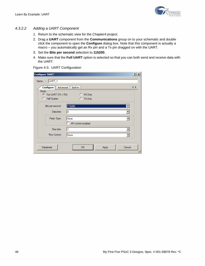
46 My First Five PSoC 3 Designs, Spec. # 001-58878 Rev. *C
Learn By Example: UART
4.3.2.2 Adding a UART Component
1. Return to the schematic view for the Chapter4 project.
2. Drag a UART component from the Communications group on to your schematic and double click the component to open the Configure dialog box. Note that this component is actually a macro – you automatically get an Rx pin and a Tx pin dragged on with the UART.
3. Set the Bits per second selection to 115200.
4. Make sure that the Full UART option is selected so that you can both send and receive data with the UART.
Figure 4-3. UART Configuration

My First Five PSoC 3 Designs, Spec. # 001-58878 Rev. *C 47
Learn By Example: UART
The other options in the Configure ‘UART’ window specify that the UART sends or receives eight bits of data at a time. We will not be sending a parity bit. The stop bit will be only one bit in length and there will not be any flow control to this communication. The computer that is con-nected to this project needs to have the same COM port settings as the UART in the PSoC 3 to communicate correctly.
Figure 4-4. UART Configuration - Advanced Settings
5. Click on the Advanced tab in the UART Configure dialog (Figure 4-4 on page 47).
The Clock Selection defaults to Internal Clock. This tells PSoC Creator to configure the internal clocking distribution system to provide the necessary input frequency to the UART component. If External Clock is selected, then a clock terminal will appear in schematic view to allow you to connect a clock signal from another component in your design. The external clock signal needs to have a frequency that is eight times the desired bit rate. This faster signal allows the UART component to over-sample the incoming data and align the data sampling with the center of each bit transmitted by another device. This oversampling helps with data integrity and proper error detection.
6. Clear all selection boxes in the Interrupts section of the Advanced tab.
7. Scroll to the bottom of the Advanced tab and clear the Hardware TX-Enable option.
8. Set the buffer size for RX and TX to 4 (Figure 4-5).

48 My First Five PSoC 3 Designs, Spec. # 001-58878 Rev. *C
Learn By Example: UART
When the buffer sizes for RX and TX are less than or equal to four, the options to enable internal interrupts for the RX ISR and TX ISR are grayed out. You can enable external interrupts. The PSoC 3 device implements a 4-byte buffer for RX and TX with the UART component. This relieves the CPU of the need to manage the UART for every byte sent or received. If you want a larger than 4-byte buffer, then PSoC Creator will generate the code needed to implement a larger buffer using interrupts and additional RAM resources to manage that buffer. The calls to read and write from the buffers are the same regardless of buffer size.
Figure 4-5. UART Configuration - Advanced Settings (continued)

My First Five PSoC 3 Designs, Spec. # 001-58878 Rev. *C 49
Learn By Example: UART
4.3.2.3 Adding a Digital I/O Component
1. The Rx and Tx pins have already been dragged onto the schematic for you. All you have to do is rename them to Rx_Pin and Tx_Pin, respectively, and make it point 1.
2. Add a logic low signal to the reset input of UART_1.
Your schematic should look like Figure 4-6.
Figure 4-6. Chapter4 Schematic
4.3.3 Assigning Pins
1. Open the Chapter4.cydwr file.
2. Click on the Pins tab.
3. Assign the Tx_Pin to P1[7] and the Rx_Pin to P1[4] as shown in Figure 4-7.
4. Select Build Chapter4 from the Build menu and verify that you do not have any errors.
Figure 4-7. Chapter 4 Pin Assignment
4.3.4 Configuring Clocks
The clock signal for the UART_1 component must be generated from the clocking resources with thePSoC. PSoC Creator configures the registers as needed to create this clock for you. Click on theClocks tab inside the Chapter4.cydwr file to examine how PSoC Creator has configured these clocks(Figure 4-8 on page 50). The clocks that are in blue are the clocks needed by the components in theChapter4 design.
The clock_PWM that we are using for our main timer is set to be 100 kHz. PSoC Creator decided toderive this 100 kHz from the IMO (Internal Main Oscillator) which is running at 3 MHz. IMO is listedas the input clock on the far right column. It sets up a divider 30 to reduce the frequency to 100 kHz.

50 My First Five PSoC 3 Designs, Spec. # 001-58878 Rev. *C
Learn By Example: UART
The divider produces an actual frequency that matches the desired frequency. Therefore, the accu-racy of the 100 kHz that we desire is only dependent on the accuracy of the IMO frequency.
Figure 4-8. Clock Configuration
Examine the UART_1_IntClock. The UART_1 component bit rate is set to 115,200 bits per second.Earlier, we learned that the UART needs to over-sample each bit that is being received so that theUART can provide good error detection and ensure data integrity. The required clock for theUART_1 component must be eight times the 115,200 bits per second. This gives us a frequency of921,600 bits per second. PSoC Creator is showing a desired frequency of 921.600 kHz for theUART_1_IntClock. However, it is not able to divide any of the available clocks by an integer value toachieve 921.600 kHz, so it chooses the closest integer possible. The source clock is the masterclock which is running at 24 MHz. PSoC Creator divides this clock by 26 which results in an actualfrequency of approximately 923.077 kHz. That might seem like a large error to be off by more than1.5 kHz, however, the percentage of error between the actual clock and the desired clock is onlyabout 0.16%. This error is acceptable for communication with the computer.
You will notice that some of the clocks listed in the light tan have a ‘?’ listed under the Actual Fre-quency column. These frequencies require an external crystal or clock signal which we are not goingto have for this project. The other clocks listed in the light tan area are derived from the internal clocksources of the PSoC device. Double click in the light tan area to examine this arrangement(Figure 4-9 on page 51).
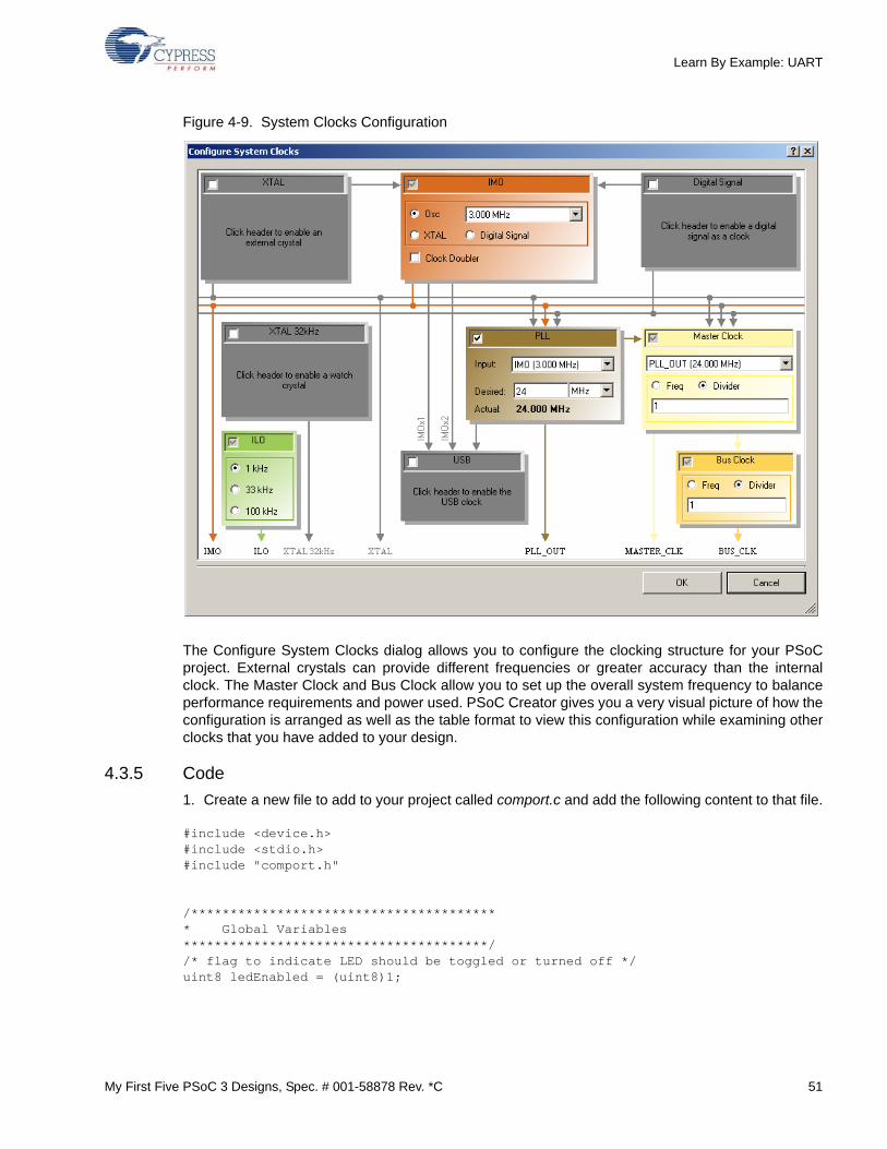
My First Five PSoC 3 Designs, Spec. # 001-58878 Rev. *C 51
Learn By Example: UART
Figure 4-9. System Clocks Configuration
The Configure System Clocks dialog allows you to configure the clocking structure for your PSoCproject. External crystals can provide different frequencies or greater accuracy than the internalclock. The Master Clock and Bus Clock allow you to set up the overall system frequency to balanceperformance requirements and power used. PSoC Creator gives you a very visual picture of how theconfiguration is arranged as well as the table format to view this configuration while examining otherclocks that you have added to your design.
4.3.5 Code
1. Create a new file to add to your project called comport.c and add the following content to that file.
#include <device.h>#include <stdio.h>#include "comport.h"
/**************************************** Global Variables***************************************//* flag to indicate LED should be toggled or turned off */uint8 ledEnabled = (uint8)1;
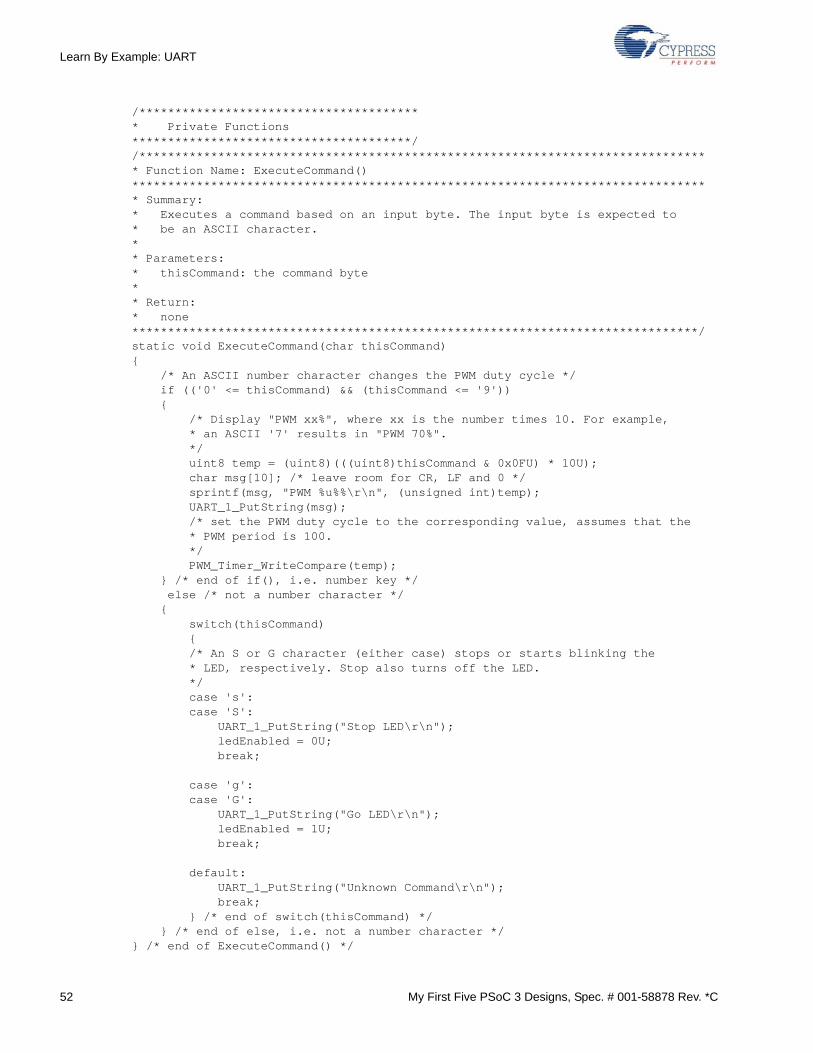
52 My First Five PSoC 3 Designs, Spec. # 001-58878 Rev. *C
Learn By Example: UART
/**************************************** Private Functions***************************************//******************************************************************************** Function Name: ExecuteCommand()********************************************************************************* Summary:* Executes a command based on an input byte. The input byte is expected to* be an ASCII character.** Parameters:* thisCommand: the command byte** Return:* none*******************************************************************************/static void ExecuteCommand(char thisCommand){ /* An ASCII number character changes the PWM duty cycle */ if (('0' <= thisCommand) && (thisCommand <= '9')) { /* Display "PWM xx%", where xx is the number times 10. For example, * an ASCII '7' results in "PWM 70%". */ uint8 temp = (uint8)(((uint8)thisCommand & 0x0FU) * 10U); char msg[10]; /* leave room for CR, LF and 0 */ sprintf(msg, "PWM %u%%\r\n", (unsigned int)temp); UART_1_PutString(msg); /* set the PWM duty cycle to the corresponding value, assumes that the * PWM period is 100. */ PWM_Timer_WriteCompare(temp); } /* end of if(), i.e. number key */ else /* not a number character */ { switch(thisCommand) { /* An S or G character (either case) stops or starts blinking the * LED, respectively. Stop also turns off the LED. */ case 's': case 'S': UART_1_PutString("Stop LED\r\n"); ledEnabled = 0U; break;
case 'g': case 'G': UART_1_PutString("Go LED\r\n"); ledEnabled = 1U; break;
default: UART_1_PutString("Unknown Command\r\n"); break; } /* end of switch(thisCommand) */ } /* end of else, i.e. not a number character */} /* end of ExecuteCommand() */

My First Five PSoC 3 Designs, Spec. # 001-58878 Rev. *C 53
Learn By Example: UART
/**************************************** Global Functions***************************************//******************************************************************************** Function Name: InitComPort ()*******************************************************************************/void InitComPort(void){ UART_1_Start(); /* delay for the UART to initialize */ CyDelay(1LU); /* msec */ UART_1_PutString("My First Five Designs\r\n");} /* end of InitComPort() */
/******************************************************************************** Function Name: UpdateComPort*******************************************************************************/void UpdateComPort(void){ /* if the UART has a received byte, execute a command based on that byte */ if(UART_1_ReadRxStatus() & (uint8)UART_1_RX_STS_FIFO_NOTEMPTY) { ExecuteCommand((char)UART_1_ReadRxData()); }} /* end of UpdateComPort() */
2. Create a new header file for your project called comport.h and add the following content to that file. Include this file in main.c.
/******************************************************************************** Function Name: InitComPort()********************************************************************************* Summary:* Sets up the UART for operation and sends out a message.** Parameters:* none** Return:* none*******************************************************************************/void InitComPort(void);
/******************************************************************************** Function Name: UpdateComPort********************************************************************************* Summary:* Checks for any received bytes and calls executes commands as needed, based* on those bytes. It is expected that the received bytes are ASCII characters* as follows:* '0' - '9' : set the PWM duty cycle to 0%, 10%, ..., 90%* 'S', 's' : stop the blinking LED, turning it off.* 'G', 'g' : start blinking the LED.** In addition to the above actions, a corresponding message is sent out the* UART transmit. This includes an error message if the received byte is not* one of the above characters.

54 My First Five PSoC 3 Designs, Spec. # 001-58878 Rev. *C
Learn By Example: UART
** This routine should be called every millisecond.** Parameters:* none** Return:* none*******************************************************************************/void UpdateComPort(void);
/**************************************** Global Variables***************************************//* This flag is used to indicate whether or not a command has been received from* the ComPort to enable or disable the blinking LED.*/extern uint8 ledEnabled;
3. Now place the call to intializeComPort in the main routine and place the call to the UpdateComPort function in the millisecond area as shown below. Don’t forget to include comport.h.
InitTiming(); /* interrupt */ PWM_Timer_Start(); /* source of interrupt */ CYGlobalIntEnable /* macro */ CharLCD_Start(); /* Start the CharLCD component */ InitComPort(); /* UART component */...... /* This section contains code to be executed every millisecond */ if(milliSecond) { milliSecond = 0U; /* poll the UART and execute a command if bytes received */ UpdateComPort(); } /* end of millisecond section */......
The InitComPort call in the beginning of main will both start the UART_1 component and send astring through that ComPort to your computer. In order to see this message, you will need to havethe computer terminal program running and set to the same parameters as the UART_1 componentwhen the debugger executes this code. The UpdateComPort is called every millisecond to see if acharacter has arrived from the computer, respond to any character received, and send out theappropriate response. See the ExecuteCommand function. Note that UART_1_PutString will loopand not return until all the characters are sent. This may not be desirable for your project, but it is anacceptable characteristic for our purposes in this chapter.
I have limited the commands in this project to single characters for simplicity. This simplifies thereceive process by removing the need to align to the beginning of a command sequence. If a com-mand is received that is not understood, it is simply discarded. Commands can easily be sent withany terminal program, such as Hyperterminal or Tera Term. The number keys will change the dutycycle of the PWM_Timer PWM output and therefore the brightness of the LED attached to thePWM_Pin. The S and G commands change the value of ledEnabled. We need to modify the tog-gleLED function in main.c to utilize ledEnabled. It should toggle the LED if the ledEnabled is a nonzero value and it should shut the LED off if ledEnabled is equal to zero. Here is the modified tog-gleLED function.

My First Five PSoC 3 Designs, Spec. # 001-58878 Rev. *C 55
Learn By Example: UART
/**************************************************** Function Name: ToggleLed()***************************************************** Summary:* Toggles or turns off the LED, depending on an enable state.** Parameters:* none** Return:* none****************************************************/void ToggleLed(void){ /* toggle the LED if it is enabled, otherwise just keep it turned off */ if(ledEnabled) { /* Set the pin to the opposite of what is read from the pin. The pin * value is always right-justified to the LS bits. */ LED_Pin_Write(LED_Pin_Read() ^ 1U); } else { LED_Pin_Write(0U); }} /* end of ToggleLed() */
4.3.6 Building and Debugging Your Project
Build the project and verify that it compiles without any errors. Connect the additional pins neededfor the UART (Figure 4-10 on page 56).

56 My First Five PSoC 3 Designs, Spec. # 001-58878 Rev. *C
Learn By Example: UART
Figure 4-10. Pin Connections for Chapter4
1. Before downloading the code to the project, connect the computer to the serial port connector on the DVK1 board
2. Set up communication using hyper terminal.Start->All Programs->Accessories->Communication->Hyper Terminal-> in 'Connection Descrip-tion' set name as -XYZ click ok->in 'Connect to' select 'Connect Using'-COM1/COM2 based on the serial port selected for UART.
3. Download the code to the PSoC and run the program. You should see the message “My First Five Designs” returned to the terminal window.
4. Press the [S] key on the keyboard to turn off the LED connected to the LEDPin.
5. Press the [G] key on the keyboard. The LED should start blinking again.
6. Press each of the number keys to observe the different duty cycle rates to the LED connected to the PWM_Pin. The [0] key sets the duty cycle to 0%, which just holds the signal low and turns off the LED.
4.4 Conclusions
Two-way communication with a PC is a very powerful tool for any embedded designer. A simpleUART connection allows our project to benefit from the rich interface and display capabilities of acomputer. The UART connection can serve as a real-time debugging tool during operation.
The format of communication for the UART makes it a good choice for a part-time debugging tool.Since the communication does not require a response from the computer in order to continue, you

My First Five PSoC 3 Designs, Spec. # 001-58878 Rev. *C 57
Learn By Example: UART
can leave a computer disconnected with the debugging code active. A computer can be connectedto the project for debugging at any time without restarting the project.
4.5 Additional Information
The UART remains a favorite serial communication device on many embedded devices today.Nearly every desktop computer of earlier generations supported two UARTs. They were referred toas COM ports. The COM port on your computer allowed you a quick connection to all sorts ofembedded devices. The COM ports on those early desktop computers would have a control chipthat handled the serial communications. The most popular serial port control chip in earlier comput-ers was the National 16550. Similar devices were soon made by other manufacturers. The 16550included FIFO (First In First Out) buffers for communication that allowed the reception or transmis-sion of multiple bytes without processor intervention.
There are many reasons why the common UART has remained so popular. First of all, it is a serialcommunication so the amount of pins needed to communicate are very low. In fact, most UARTdesigns that I have done only used two pins: transmit and receive. There are some other pins avail-able on a computer COM port that can be used to regulate the flow of data. However, for now we willconcentrate on the transmit and receive pins. When you forgo the lines that control that flow of data,you need to make sure that each side of the communication takes care not to send data faster thanthe other side can receive and process the data. Since the transmit and receive lines are separate,you can be receiving data at the same time that you are transmitting data. This is known as fullduplex communication.
The COM ports on computers follow the RS232 standard. This standard denotes a voltage rangethat is higher than most microcontrollers can safely handle. The higher voltages in the specificationallow for a wider range of acceptable voltages on the receiving end. The higher voltages also helpwith higher capacitance that becomes a larger and larger problem as the wires get longer. If youwant to follow the voltage standard, you usually need to add a chip to translate the voltages to meetthe specification. However, you can get by with some COM ports by simply using a 5V inverter fortransmitting and a resistor divider for receiving the higher voltages.
In later generations of computers the function of the serial ports that were handled by the 16550chips were combined with the functionality of the parallel ports into one chip called a super I/O chip.Later, serial ports started to disappear from computers altogether as USB became the more popularserial connection to the desktop or laptop computer. The need for UART connectivity did not disap-pear as fast as the UART disappeared from the typical home computer so a market for USB to Serialdevices grew rapidly to fill that particular need. The popularity of the UART on the microcontrollerhas remained strong. The implementation of the UART does not take a tremendous amount of cir-cuitry and the communication method is basic and straightforward. The implementation also allowsfor some error checking.
The communication over the UART is referred to as NRZ (Non Return to Zero) communication. NRZcommunication describes a signal that only has two levels. The idle state of the signal is actually thesame voltage as one of the data values. The two states for the UART signals are called a Space anda Mark. The Space is a logic zero and is defined in the RS232 protocol from +3V to +25V. The Markis a logic one and is defined from -3V to -25V. The space between -3V and +3V is undefined. Thatexplains why the use of a 5V inverter chip I mentioned above is not going to work all the time as it isnot going negative for its Mark signal and thereby falls out of the RS232 standard's definition for aMark.
When no information is being transmitted, the signal line remains in the Space voltage range. Whena byte needs to be transmitted, a Mark signal is sent. This is called a Start bit. The Start bit is fol-lowed by the least significant bit followed in order until the most significant bit of the byte is sent. Theeighth bit of data is followed by a Stop bit. The PSoC UART also supports the option to send more
58 My First Five PSoC 3 Designs, Spec. # 001-58878 Rev. *C
Learn By Example: UART
than one Stop bit per byte in addition to sending a parity bit to match with desired system require-ments. The parity bit is for error detection.
Each data bit in the UART communication including the start bit and stop bit are sent for a specifictime duration. The time duration of each bit needs to be established to interpret the communication.A device will typically sample the signal several times each bit to be able to center data samplingtowards the middle of the bit time and to verify that the signal is not noisy. The rate that bits are ableto be sent is referred to as bits per second (bps). The number of bits per second can be shown inthousands of bits per second by the term kilobits per second (kbps), or in millions of bits per second(Mbps). In order to have successful communication between devices, it is necessary that they allhave a clock that is accurate to within about 2%. This assures that each side can time the communi-cation correctly. The bits per second describes the transfer rate of data. There is another term thatyou may have heard called baud rate. The use of baud rate very often means the bit rate. However,there are times that the baud rate and bit rate are different. The term baud rate can also specificallymean the rate at which the state of the transmission signal changes.
The PSoC implementation of the UART is very flexible. Using the clocking system, you are able togenerate virtually every standard baud rate. The UART block supports 5- to 9-bit data transfer with aconfigurable number of stop bits to assure compatibility with other systems. If you are only going tocommunicate with a local system that is running at the same voltage as the PSoC device, then thereis not a need to get the voltage converter chip to step up to the higher voltages required by theRS232 standard.
My First Five PSoC 3 Designs, Spec. # 001-58878 Rev. *C 59
5. Learn By Example: CapSense
5.1 Project Overview
This chapter demonstrates how to configure the CY8C38xxx to perform capacitive sensing with yourDVK1 PCB. Cypress uses the term CapSense to describe capacitive sensing. The CapSenseproject includes two buttons and a slider that are integrated into the DVK1 PCB.
5.2 Project Background Information
CapSense is everywhere from lamps to elevators. CapSense allows a robust detection of the humanfinger with a light touch and without any moving parts. Because there are no moving parts, thenumber of switch detections is unlimited. The PCB can be fully sealed away from the user's touch,giving the design complete isolation from the environment, including static discharge andcontamination of fluids and dirt. CapSense can be used for proximity detection, detecting a fingerclose to a spinning blade or potential pinch point. CapSense is ideal for an industrial environmentbecause the switch never wears out or needs repair. It is inexpensive to implement and can be madein virtually any size and shape. CapSense is just cool.
CapSense has added a new level in the functionality of consumer electronics. Sliders can be used tointerpolate hundreds of positions from a small number of sensing elements. This ability makesCapSense ideal for game control, settings adjustments, and fine positioning. CapSense can beimplemented on PCBs, flex circuits, polyester membranes, and touchscreens. A capacitivetouchscreen has much better clarity and durability than a resistive touchscreen. CapSense iscapable of multi-touch and gesturing. It can track multiple fingers simultaneously and can interpretmovement of the fingers to add new possibilities to the user interface.
The basic process in capacitive sensing is to measure a change in capacitance that is caused by theapproach of a finger or other conductive object that can affect capacitance. There are many differentmethods to measure this capacitance. Different methods have different strengths and weaknesses inareas such as sensitivity, speed, and immunity to noise. Even though any conductive object may besensed, this chapter refers only to sensing a finger.
This chapter implements two buttons and a slider. The CapSense area of the DVK1 is directly belowthe prototyping area and includes the label CAPSENSE in the white silkscreen lettering on the PCB.P0_5 and P0_6 are CapSense buttons. The buttons indicate whether a finger is present. The sliderarea, P0_0 to P0_4, gives us a linear position of the finger on the slider area. There are only fivesignals here that are sensed by the PSoC device. The CY8C38xxx interpolates your finger's positionrelative to the five sensors using the amount of change in capacitance. It can thereby derive 100positions from only five sensors.

60 My First Five PSoC 3 Designs, Spec. # 001-58878 Rev. *C
Learn By Example: CapSense
5.3 Operation
The capacitance measurement on the circuit is very sensitive. The circuit is sensitive to changes intemperature, humidity, voltage, and so on. The capacitive system must be tuned and adjusted for theboard layout and the environment in which it operates. The configuration of CapSense parametersrelates to how much variance can be achieved in the capacitive value. When the finger approachesthe CapSense sensors, the capacitance increases because the capacitance of the finger withrespect to circuit ground is in parallel with the capacitance of sensing I/O pin with respect to circuitground.
Figure 5-1. Cross Section of a Capacitive Sensor
The code for the CapSense project establishes a Baseline measurement. The Baseline value is thevalue of capacitance measured when no finger or object is present. This value is subject to somenatural variance from reading to reading as well as drift in average measurements due to changingenvironmental conditions. To compensate for the reading noise, a Noise Threshold is used. If thechange in reading compared to the previous Baseline is less than the Noise Threshold, then theBaseline is adjusted by a percentage of that change to compensate for noise due to changingenvironmental conditions.
The Finger Threshold is a value used to determine if the button is ON or OFF. If the differencebetween new reading and Baseline is above the Finger Threshold, then the button is determined ason; otherwise, it is off. The Debounce setting introduces a debouncing mechanism and removes anyhigh-amplitude noise. If the Debounce value is set to a value other than 1, the button must be on forthat number of scans to be determined as on. There is an adjustable Hysteresis value around theFinger Threshold to handle small deviations above and below the Finger Threshold.
5.4 Project Steps
5.4.1 Adding a Project
1. Create a new project in your workspace called Chapter5. Since this is just a test project for CapSense, there is no need to recreate the work done in Chapters 3 and 4.
2. Add a Character LCD component you did in Chapter 4.

My First Five PSoC 3 Designs, Spec. # 001-58878 Rev. *C 61
Learn By Example: CapSense
5.4.2 Adding and Configuring a CapSense_CSD Component
1. Add a CapSense_CSD component by dragging the component from the CapSense group in the Component Catalog to your design.
2. Double click on the CapSense_1 component to open the Configure dialog.
3. Change the name from CapSense_1 to CapSense.
4. In the General tab, set the parameters as follows (see Figure 5-2).
Figure 5-2. CapSense Configuration General Tab
❐ Tuning method: Auto-tuning is used in this project, so the firmware sets the parameters. You do not need to tune the component parameters.
❐ Number of channels: The PSoC 3 and PSoC 5 devices have resources to scan two sensors at a time. One set of resources is on the left side and another set of resources is on the right side of the device. The number of channels is set to 1; only a single set of resources is used. When set to two channels, resources at both sides are used and two sensors are scanned at a time. If the number of sensors in the application is more than 20, it is best to use two channels. In this example project, there are only seven sensors. Therefore, only one channel is used.
❐ Raw Data Noise Filter: The filters should be used in applications where noise is significantly high. When using this example project on DVK1, the noise level is low, so the filters are not used.
❐ Water proofing and detection: Because this is not a water-proofing design, this feature is not used in this project.
❐ Scan Clock: This provides the clock to the CapSense block and can be between 3 and 24 MHz.

62 My First Five PSoC 3 Designs, Spec. # 001-58878 Rev. *C
Learn By Example: CapSense
5. Add and configure the Buttons in the Widget Config tab as shown in Figure 5-3.
Figure 5-3. Button Parameters
Select the Buttons widget and click on Add Button to add the linear slider to the design
❐ Finger Threshold: Threshold value that firmware uses to decide whether a button is on or off. It is set by auto-tuning while it tunes the sensor. Because the project uses the auto-tuning method, this parameter does not need to be set.
❐ Noise Threshold: Noise level to the firmware. The counts above the noise level are not considered as noise but as a signal (difference count). The baseline count is updated only when the raw count is within the noise threshold. The noise threshold is set by auto-tuning while it tunes the sensor. Because the project uses the auto-tuning method, this parameter does not need to be set.
❐ Hysteresis: This parameter adds the differential hysteresis on the finger threshold and reduces the noise effect. It is set by auto-tuning while it tunes the sensor. Because the project uses the auto-tuning method, this parameter does not need to be set.
❐ Debounce: If debounce is set to 5, it means that the button will be detected as “on.” It should be active for five consecutive scans. This parameter should be set manually; auto-tuning does not set it. Debounce removes high-amplitude high-frequency noise. In this project, it is set to 1 assuming that no noise is present. The debounce value of 1 makes the button sensing faster because only one scan is needed to detect the button as active.
❐ Scan Resolution: Resolution of CapSense measurement for the sensor. Higher scan resolution gives better sensitivity and SNR but it takes longer to scan the sensor. It is set by auto-tuning. Because the project uses the auto-tuning method, this parameter does not need to be set.
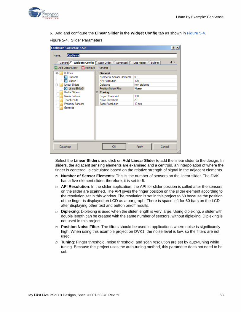
My First Five PSoC 3 Designs, Spec. # 001-58878 Rev. *C 63
Learn By Example: CapSense
6. Add and configure the Linear Slider in the Widget Config tab as shown in Figure 5-4.
Figure 5-4. Slider Parameters
Select the Linear Sliders and click on Add Linear Slider to add the linear slider to the design. Insliders, the adjacent sensing elements are examined and a centroid, an interpolation of where thefinger is centered, is calculated based on the relative strength of signal in the adjacent elements.
❐ Number of Sensor Elements: This is the number of sensors on the linear slider. The DVK has a five-element slider; therefore, it is set to 5.
❐ API Resolution: In the slider application, the API for slider position is called after the sensors on the slider are scanned. The API gives the finger position on the slider element according to the resolution set in this window. The resolution is set in this project to 60 because the position of the finger is displayed on LCD as a bar graph. There is space left for 60 bars on the LCD after displaying other text and button on/off results.
❐ Diplexing: Diplexing is used when the slider length is very large. Using diplexing, a slider with double length can be created with the same number of sensors, without diplexing. Diplexing is not used in this project.
❐ Position Noise Filter: The filters should be used in applications where noise is significantly high. When using this example project on DVK1, the noise level is low, so the filters are not used.
❐ Tuning: Finger threshold, noise threshold, and scan resolution are set by auto-tuning while tuning. Because this project uses the auto-tuning method, this parameter does not need to be set.

64 My First Five PSoC 3 Designs, Spec. # 001-58878 Rev. *C
Learn By Example: CapSense
7. In the Scan Order tab, set the parameters as follows (see Figure 5-5).
Figure 5-5. CapSense Configuration Scan Order Tab
The Scan Order tab sets the order in which the widgets are scanned. You can move the widgetsup and down in this tab to change the scan order.
❐ IDAC Value: This is the IDAC current for different sensors. It is set by auto-tuning while it tunes the sensor. Because the project uses the auto-tuning method, this parameter does not need to be set.
❐ Sensitivity: This parameter indicates the sensitivity of the capacitive system toward the finger touch. There are four sensitivity levels available, 1 being the most sensitive and 4 being the least. The sensitivity parameter needs to be set to a lower value for designs having thicker overlay or smaller sensors. In this project, this parameter is set to 4 because the DVK1 does not have any overlay on it, by default.

My First Five PSoC 3 Designs, Spec. # 001-58878 Rev. *C 65
Learn By Example: CapSense
8. In the Advanced tab, set the parameters as follows (see Figure 5-6).
Figure 5-6. CapSense Configuration Advanced Tab
❐ Analog Switch Drive Source: This is a clock divider that divides the CapSense clock and generates the switching clock (SWCLK). It is highlighted in red in Figure 5-6. The resource for the divider is selected as UDB Timer in this project.
❐ Analog Switch Divider: This is a divider value by which the CapSense clock is divided to get the switching clock (SWCLK). It is highlighted in red in Figure 5-6. It is set by auto-tuning while it tunes the sensor. Because the project uses the auto-tuning method, this parameter does not need to be set.
❐ Scan Speed: The scan speed sets the clock divider value for the SAMPCLK (highlighted in blue in Figure 5-6). The value of this clock affects the scan time. See the component datasheet to see scan times for different combinations of resolution and scan speed. The scan time is set to Normal in this project.

66 My First Five PSoC 3 Designs, Spec. # 001-58878 Rev. *C
Learn By Example: CapSense
❐ PRS EMI Reduction: PRS (pseudo random sequence) is used to reduce the EMI by spreading energy over a wider frequency spectrum. When auto-tuning is used, this value is automatically set to 16-bit PRS.
❐ Sensor Auto Reset: When enabled, the baseline is always updated regardless of whether the difference counts are above or below the noise threshold. It is Disabled in this project.
❐ Widget Resolution: The widget resolution is the resolution for the difference count or a signal. For most applications, 8-bit resolution of 8 is ideal. It is set to 8-bit in this project.
❐ Shield: This is used when CapSense should work when water droplets or water film appears on it. It is not used in this project.
❐ Inactive Sensor Connection: The inactive sensor connection should be set to Ground for most of the applications. When a shield is used, it should be connected to the shield. In this project, because the shield is not used, it is set to Ground.
❐ Guard Sensor: Used when water proofing is required. In this project it is Disabled.
❐ Current Source: The IDAC sourcing/sinking or external bleeding resistance can be used in CapSense sigma-delta. Auto-tuning supports only IDAC Sourcing.
❐ IDAC Range: When auto-tuning is used, this is automatically set to 255 uA.
❐ Digital Resource Implementation: The resource for the digital logic in the CapSense can be selected as UDB Timer or fixed-function timer. In this project, it is set to UDB Timer.
❐ Voltage Reference Source: The reference voltage for CapSense can be either 1.024-V bandgap reference voltage or VDAC with a value between 0 V and 4 V. When auto-tuning is used, it is automatically set to Vref 1.024V.
5.4.2.1 Assigning Pins
1. Assign the pins for the CapSense elements in the design-wide resources file (Figure 5-7).
2. The Alias name Cmod_CH0 is for a capacitor that you must add to your design. If you look at the schematic of the CY8C38 Family Processor Module you will see that a 2200-pF capacitor (C18) is included on the processor module for use as the CMOD capacitor. It is attached to pin P2_7 on the processor module. Choose pin P2[7] for Cmod_CH0.
3. The other pin assignments follow the port numbers as seen on the white silkscreen text of the DVK1 PCB in the CapSense area.
Figure 5-7. CapSense Pin Assignments
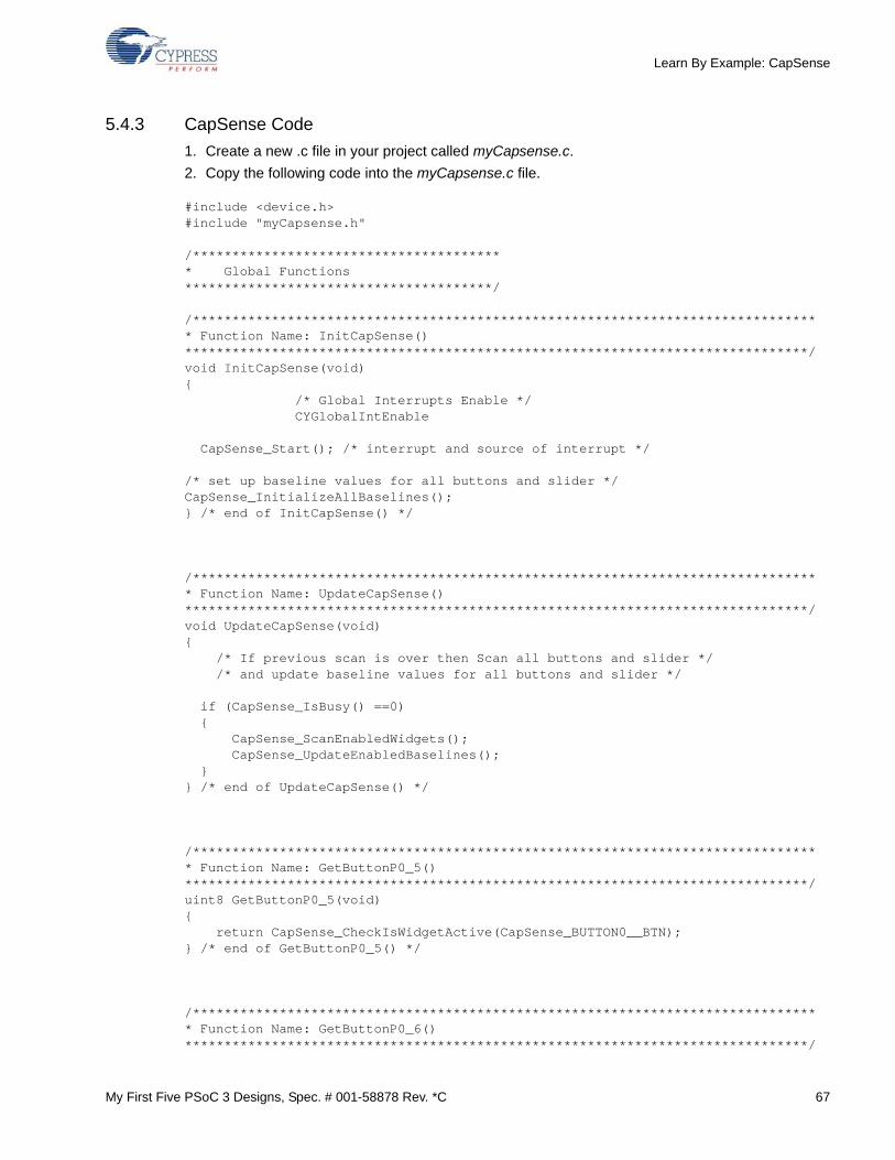
My First Five PSoC 3 Designs, Spec. # 001-58878 Rev. *C 67
Learn By Example: CapSense
5.4.3 CapSense Code
1. Create a new .c file in your project called myCapsense.c.
2. Copy the following code into the myCapsense.c file.
#include <device.h>#include "myCapsense.h"
/**************************************** Global Functions***************************************/
/******************************************************************************** Function Name: InitCapSense()*******************************************************************************/void InitCapSense(void){ /* Global Interrupts Enable */ CYGlobalIntEnable
CapSense_Start(); /* interrupt and source of interrupt */ /* set up baseline values for all buttons and slider */CapSense_InitializeAllBaselines();} /* end of InitCapSense() */
/******************************************************************************** Function Name: UpdateCapSense()*******************************************************************************/void UpdateCapSense(void){ /* If previous scan is over then Scan all buttons and slider */ /* and update baseline values for all buttons and slider */
if (CapSense_IsBusy() ==0){ CapSense_ScanEnabledWidgets(); CapSense_UpdateEnabledBaselines();}
} /* end of UpdateCapSense() */
/******************************************************************************** Function Name: GetButtonP0_5()*******************************************************************************/uint8 GetButtonP0_5(void){ return CapSense_CheckIsWidgetActive(CapSense_BUTTON0__BTN);} /* end of GetButtonP0_5() */
/******************************************************************************** Function Name: GetButtonP0_6()*******************************************************************************/

68 My First Five PSoC 3 Designs, Spec. # 001-58878 Rev. *C
Learn By Example: CapSense
uint8 GetButtonP0_6(void){ return CapSense_CheckIsWidgetActive(CapSense_BUTTON1__BTN);} /* end of GetButtonP0_6() */
/******************************************************************************** Function Name: GetSlider()*******************************************************************************/uint8 GetSlider(void){ return (uint8)CapSense_GetCentroidPos(CapSense_LINEARSLIDER0__LS);} /* end of GetSlider() */
3. Create a header file called myCapsense.h and include the following code in that file.
/******************************************************************************** Function Name: InitCapSense()********************************************************************************* Summary:* Initializes the CapSense component for the DVK.** Parameters:* none** Return:* none*******************************************************************************/void InitCapSense(void);
/******************************************************************************** Function Name: UpdateCapSense()********************************************************************************* Summary:* Scans slots and updates baselines for the CapSense component for the DVK.** Parameters:* none** Return:* none*******************************************************************************/void UpdateCapSense(void);
/******************************************************************************** Function Name: GetButtonP0_5********************************************************************************* Summary:* Reports if a finger is present or not at DVK button P0_5.** Parameters:

My First Five PSoC 3 Designs, Spec. # 001-58878 Rev. *C 69
Learn By Example: CapSense
* none** Return:* 1 if finger is present, 0 if finger is not present*******************************************************************************/uint8 GetButtonP0_5(void);
/******************************************************************************** Function Name: GetButtonP0_6********************************************************************************* Summary:* Reports if a finger is present or not at DVK button P0_6.** Parameters:* none** Return:* 1 if finger is present, 0 if finger is not present*******************************************************************************/uint8 GetButtonP0_6(void);
/******************************************************************************** Function Name: GetSlider********************************************************************************* Summary:* Reports the presence / position of a finger on the DVK slider.** Parameters:* none** Return:* Position 0 - 100 if finger is present, 0xFF if finger is not present*******************************************************************************/uint8 GetSlider(void);
4.Copy the following code into the main.c file.
#include <device.h>#include <myCapsense.h>
void main(){ /* This function enables the global interrupts
* Starts the CapSense component* Initializes all the baselines*/
InitCapSense();
/* Print label information on the LCD */ CharLCD_Start(); CharLCD_Position(0,0); CharLCD_PrintString("P05 P06 Slider");
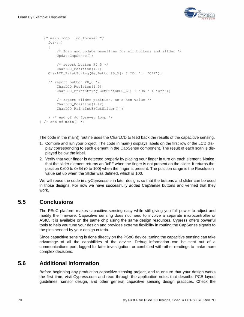
70 My First Five PSoC 3 Designs, Spec. # 001-58878 Rev. *C
Learn By Example: CapSense
/* main loop - do forever */ for(;;) { /* Scan and update baselines for all buttons and slider */ UpdateCapSense();
/* report button P0_5 */ CharLCD_Position(1,0);
CharLCD_PrintString(GetButtonP0_5() ? "On " : "Off");
/* report button P0_6 */ CharLCD_Position(1,5); CharLCD_PrintString(GetButtonP0_6() ? "On " : "Off");
/* report slider position, as a hex value */ CharLCD_Position(1,12); CharLCD_PrintInt8(GetSlider());
} /* end of do forever loop */} /* end of main() */
The code in the main() routine uses the CharLCD to feed back the results of the capacitive sensing.
1. Compile and run your project. The code in main() displays labels on the first row of the LCD dis-play corresponding to each element in the CapSense component. The result of each scan is dis-played below the label.
2. Verify that your finger is detected properly by placing your finger in turn on each element. Notice that the slider element returns an 0xFF when the finger is not present on the slider. It returns the position 0x00 to 0x64 (0 to 100) when the finger is present. The position range is the Resolution value set up when the Slider was defined, which is 100.
We will reuse the code in myCapsense.c in later designs so that the buttons and slider can be usedin those designs. For now we have successfully added CapSense buttons and verified that theywork.
5.5 Conclusions
The PSoC platform makes capacitive sensing easy while still giving you full power to adjust andmodify the firmware. Capacitive sensing does not need to involve a separate microcontroller orASIC. It is available on the same chip using the same design resources. Cypress offers powerfultools to help you tune your design and provides extreme flexibility in routing the CapSense signals tothe pins needed by your design criteria.
Since capacitive sensing is done directly on the PSoC device, tuning the capacitive sensing can takeadvantage of all the capabilities of the device. Debug information can be sent out of acommunications port, logged for later investigation, or combined with other readings to make morecomplex decisions.
5.6 Additional Information
Before beginning any production capacitive sensing project, and to ensure that your design worksthe first time, visit Cypress.com and read through the application notes that describe PCB layoutguidelines, sensor design, and other general capacitive sensing design practices. Check the

My First Five PSoC 3 Designs, Spec. # 001-58878 Rev. *C 71
Learn By Example: CapSense
Cypress website for the latest tools in tuning capacitive sensing. Newer tools can save you a lot oftime trying to tune your circuitry.
Take note that capacitive sensing can consume some of the analog resources. Always lay out thenecessary components of your design as soon as possible in PSoC Creator to make sure that youhave enough resources to complete your project. Configure the components and route all thesignals, even if you do not have any firmware to verify that your design is feasible in the PSoCdevice that you have selected.

72 My First Five PSoC 3 Designs, Spec. # 001-58878 Rev. *C
Learn By Example: CapSense

My First Five PSoC 3 Designs, Spec. # 001-58878 Rev. *C 73
6. Learn By Example: Digital Logic
6.1 Project Overview
This chapter demonstrates the ability to add various digital logic elements into a design. The digitallogic will be used to create a state machine for the riddle Farmer, Corn, Goose, Fox.
6.2 Project Background Information
We will add digital logic elements to our design to create a state machine based around the riddleFarmer, Corn, Goose, Fox. The riddle describes a farmer with some corn, a goose, and a fox whoneeds to get all of these across a river. There is a boat for the farmer to use, but the farmer can onlyfit one item with him on the boat to cross the river. He cannot leave the goose with the corn or thegoose will eat the corn. He cannot leave the fox with the goose, or the fox will eat the goose. Youneed to determine what order the farmer must use to take all the items to the other side of the river.There are seven steps that must be taken to get across the river. The logic will decode what step youare on, if an error condition occurs, and when you have successfully completed the task.
My first experience with the Farmer, Corn, Goose, and Fox riddle was at Utah State University. Theassignment was to construct a circuit that modeled the riddle almost entirely out of two input NANDgates. This solution took up two full bread boards with a rat’s nest of wires. This experience helpedbuild appreciation for more powerful logic and finally microcontrollers. The application of the Farmer,Corn, Goose, and Fox riddle in this chapter implements the solution using a lookup table (LUT) forthe main comparison on inputs and uses some more simple logic for error checking.
6.3 Project Steps
6.3.1 Adding a Project
1. Create a new project in your workspace called Chapter6.
2. Recreate all the components and code added in Chapters 3 and 4. We aren’t going to use the CapSense buttons in this chapter, so there is no need to duplicate the code in Chapter 5.
6.3.1.1 Setting Up Your Project
3. Before starting this implementation of logic, create a new page in the schematic to provide more room to place your logic components.
4. Right click on the Page 1 tab at the bottom of the schematic and select Add Page. This creates a Page 2 in the schematic.
5. Right click on the newly created Page 2 tab and select Rename Page.
6. Type in Digital Logic for the new page name.
7. Click on the letter T at the left of the schematic page to select the text tool. Note that you can also simply press the [t] key on your keyboard to select this tool.
8. Click and drag in the schematic to form a text box.

74 My First Five PSoC 3 Designs, Spec. # 001-58878 Rev. *C
Learn By Example: Digital Logic
9. Type the following text into your box (Figure 6-1).
Step 0 - Farmer, Corn, Goose, Fox = 0Step 1 - Corn, Fox = 0 & Farmer, Goose = 1Step 2 - Farmer, Corn, Fox = 0 & Goose = 1Step 3 - Fox = 0 & Farmer, Corn, Goose = 1Step 4 - Farmer, Goose, Fox = 0 & Corn = 1Step 5 - Goose = 0 & Farmer, Corn, Fox = 1Step 6 - Farmer, Goose = 0 & Corn, Fox = 1Step 7 - Farmer, Corn, Goose, Fox = 1
These are the steps that we are going to follow to solve the riddle. Each of the four items will be represented by a bit of logic. A value of 0 for a particular bit means that object is on the near side of the river. Likewise, a value of 1 for a bit means that item is on the far side of the river. I have not allocated a bit for the boat since the boat must always reside on the same side as the farmer. There is more than one solution for this riddle, but I am only implementing this solution for sim-plicity. If you do not follow the steps as described above, then the logic rejects the answer.
Figure 6-1. Blank Digital Logic Schematic Page
6.3.1.2 Adding and Configuring a Control Register
The logic in the PSoC can be routed to external pins, but I have chosen to control and sense thestate of the logic using control and status registers. The control and status registers allow softwareaccess to hardware signals within the PSoC. The use of registers allows us to use this logic withoutany additional connections to the DVK1.

My First Five PSoC 3 Designs, Spec. # 001-58878 Rev. *C 75
Learn By Example: Digital Logic
1. Add a Control Register to your project from the Digital-Registers group of the Component Cat-alog.
2. Double click the Control Register and configure the Name to be Control_Reg_NextStep.
3. Change the NumOutputs variable to 4. This is the driving value that puts items on one side of the river or the other. Each of the four bits represents one of the items in our riddle (Figure 6-2).
Figure 6-2. Control Register Configuration
6.3.1.3 Using Sheet Connectors
1. Place a Sheet Connector on the design. This is done by selecting the diamond-shaped Sheet Connector at the left of the schematic window or by pressing the s button in the schematic.
2. Connect bit 0 of Control_Register_NextStep to the Sheet Connector with a wire.
3. Rename the wire attached to the sheet connector by right clicking on the wire and selecting the Edit Name and Width option.
4. Clear the check mark to Use computed name and width.
5. Enter Farmer for the Name and verify that the Indices option is set to None (Figure 6-3 on page 76).
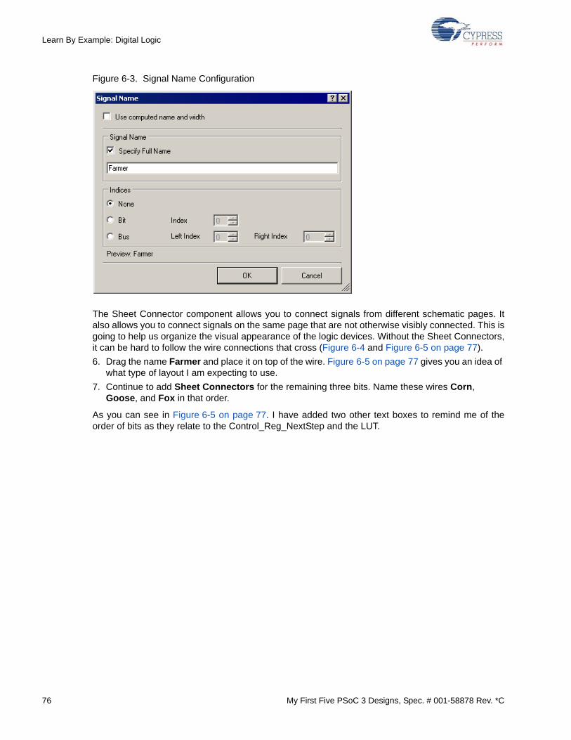
76 My First Five PSoC 3 Designs, Spec. # 001-58878 Rev. *C
Learn By Example: Digital Logic
Figure 6-3. Signal Name Configuration
The Sheet Connector component allows you to connect signals from different schematic pages. Italso allows you to connect signals on the same page that are not otherwise visibly connected. This isgoing to help us organize the visual appearance of the logic devices. Without the Sheet Connectors,it can be hard to follow the wire connections that cross (Figure 6-4 and Figure 6-5 on page 77).
6. Drag the name Farmer and place it on top of the wire. Figure 6-5 on page 77 gives you an idea of what type of layout I am expecting to use.
7. Continue to add Sheet Connectors for the remaining three bits. Name these wires Corn, Goose, and Fox in that order.
As you can see in Figure 6-5 on page 77. I have added two other text boxes to remind me of theorder of bits as they relate to the Control_Reg_NextStep and the LUT.

My First Five PSoC 3 Designs, Spec. # 001-58878 Rev. *C 77
Learn By Example: Digital Logic
Figure 6-4. Disorderly Logic
Figure 6-5. Orderly Logic

78 My First Five PSoC 3 Designs, Spec. # 001-58878 Rev. *C
Learn By Example: Digital Logic
6.3.1.4 Adding a Lookup Table
1. Add a Lookup Table to your project from the Digital-Logic group.
2. Name the Lookup Table LUT_Riddle.
3. Change the number of inputs to 4 and the number of outputs to 4.
In the table you need to set up the logic that will equate each step number with the appropriate input states. Using the text description of each step added to the project, we can fill in the table accordingly.
4. Enter 0x0F for each value that does not correspond to a step. The entries are given in order here: 0x00, 0x0F, 0x04, 0x0F, 0x02, 0x01, 0x0F, 0x03, 0x0F, 0x0F, 0x06, 0x05, 0x0F, 0x0F, 0x0F, 0x07 (Figure 6-6).
5. Connect the Farmer, Corn, Goose, and Fox sheet connectors to the LUT_Riddle inputs.ww
Figure 6-6. LUT Output Values

My First Five PSoC 3 Designs, Spec. # 001-58878 Rev. *C 79
Learn By Example: Digital Logic
6.3.1.5 Adding More Registers
1. Add another Control Register component and name the component Control_Reg_Clock.
2. Configure Control_Reg_Clock to be one bit only.
3. Connect it to a Sheet Connector and name the wire clock.
4. Add a Status Register from the Digital-Registers group.
5. Name the Status Register Status_Reg_CurrentStep and configure it to have four inputs.
6. Connect the clock wire to the clock input terminal of Status_Reg_CurrentStep.
The clock input is needed for a status register to indicate when the status register should sample the input terminals. We are going to use a Control_Reg_Clock to create a manual clock signal.
7. Connect the inputs of Status_Reg_CurrentStep to the outputs of LUT_Riddle.
8. Place Sheet Connectors on each of the wires connecting LUT_Riddle and Status_Reg_CurrentStep.
9. Name the wires step, but use the Bit option for the Indices in the wire configuration dialog to indicate whether it is bit 0, bit 1, bit 2, or bit 3 (Figure 6-7).
Figure 6-7. Clock and CurrentStep Registers
The LUT_Riddle compares each state of the Farmer, Corn, Goose, and Fox to see which step of theriddle it is on. If the step is undefined, then the output of the LUT is 0x0F. Since there is not a clockinput for the LUT_Riddle, the output pins of the LUT change immediately after the input signalschange. Note, however, that the value of Status_Reg_CurrentStep does not change until I pulse theControl_Reg_Clock value. Therefore, the process to progress to the next step in the riddle requiresme to first write to Control_Reg_NextStep and then set and clear the bit in Control_Reg_Clock. Aftercompleting those two steps, I will have the current step value in the Status_Reg_CurrentStep regis-ter.
6.3.1.6 Adding a Hardware Delay
We can add a hardware delay into our logic state machine with D Flip Flops from the Digital Logicgroup of the Component Catalog.
1. Add four D Flip Flops to the schematic.
2. Add a Sheet Connector to the left of one of the flip flops. Connect this sheet connector to the clock input of a flip flop and name the wire ‘clock’. By naming the two wires attached to sheet connectors the same you connect them logically.
3. Connect the clock wire signal to each of the other flip flops’ clock inputs.

80 My First Five PSoC 3 Designs, Spec. # 001-58878 Rev. *C
Learn By Example: Digital Logic
4. Add Sheet Connectors and connect one from each the step[0]-step[3] signals to a D Flip Flop data (d) terminal.
5. Add another Status Register to the right of the D Flip Flops.
6. Set the name to be Status_Reg_LastStep and configure it to be four bits.
7. Connect these four inputs to the outputs of the D Flip Flops.
8. Don't forget to connect the clock wire signal to the clock terminal of Status_Reg_LastStep (Figure 6-8).
Figure 6-8. D Flip Flops and Status_Reg_LastStep
Status_Reg_LastStep contains the previous value of Status_Reg_CurrentStep. We will use thisdelay to ensure we are solving the riddle in order. If I am on step 7 and I did not just come from step6, then I know that I have not completed the puzzle in order. I will check the values of these two reg-isters after each clock pulse. It is good to note that another LUT could perform this function beauti-fully without any CPU intervention and could assert an error signal, but the method chosen here willsuffice. Note also that I did not give specific names for each of the D Flip Flops. The default nameswork fine in our example because the devices are hardware logic.
Add some final error checking for the riddle. This error checking is easier to show to you than it is todescribe. Refer to Figure 6-9 on page 81. Each time a pulse is sent to the clock wire, theStatus_Reg_Error will be loaded with a bit set to the value of one (1) if the Farmer is not with theGoose and the Fox or if the Farmer is not with the Goose and the Corn. Notice that I included checksfor both sides of the river in each case.

My First Five PSoC 3 Designs, Spec. # 001-58878 Rev. *C 81
Learn By Example: Digital Logic
Figure 6-9. Error Logic
6.3.2 Code
1. Create two new files in the project called farmerRiddle.h and farmerRiddle.c.
2. Include farmerRiddle.h in the main.c file. The farmerRiddle.h file will only have three prototypes.
/**************************************** Function Prototypes***************************************//******************************************************************************** Function Name: InitRiddle()********************************************************************************* Summary:* Initializes Riddle conditions, UART communications, and the display.** Parameters:* none** Return:* none*******************************************************************************/void InitRiddle(void);
/******************************************************************************** Function Name: UpdateRiddle()********************************************************************************* Summary:* Processes commands from the UART, updating Riddle conditions and display.* Since a display update may include an animation, this function can pend for* a long time until it returns.** Parameters:* none** Return:* none*******************************************************************************/

82 My First Five PSoC 3 Designs, Spec. # 001-58878 Rev. *C
Learn By Example: Digital Logic
void UpdateRiddle(void);
/******************************************************************************** Function Name: TestRiddle()********************************************************************************* Summary:* Tests the Riddle functions.** Parameters:* none** Return:* none*******************************************************************************/void TestRiddle(void);
3. Add calls to the InitRiddle and testRiddle functions to the main.c file just before the endless loop. The TestRiddle call is usually commented out unless you want an automated method to test the rest of the project.
/* Initialize other components, not associated with interrupts */CharLCD_Start();InitComPort(); /* UART component */
/* Riddle initialization *//*TestRiddle();*/ /* optional function, typically commented out */InitRiddle();
for(;;) /* main loop - do forever */
4. Add a call in main.c in the tenth second area for UpdateRiddle.
5. Delete or comment out the DisplayCount function call because it competes for the LCD display.
6. Also delete or comment out the UpdateComPort call because it clears the UART_1 receive buffer before you get to UpdateRiddle.

My First Five PSoC 3 Designs, Spec. # 001-58878 Rev. *C 83
Learn By Example: Digital Logic
/* This section contains code to be executed every millisecond */if(milliSecond){ milliSecond = 0U; /* poll the UART and execute a command if bytes received */ /* UpdateComPort(); */ /* comment this out if doing the riddle */} /* end of millisecond section */
/* This section contains code to be executed every tenth second */if(tenthSecond){ tenthSecond = 0U; /* Toggle the LED if the button is NOT pressed. This will cause * the LED to blink rapidly when the button is NOT pressed. */ if(Button_Pin_Read()) /* read a 1 when button is NOT pressed */ { ToggleLed(); }
UpdateRiddle();} /* end of tenth second section */
The function call TestRiddle is not needed for the project, but it does run through each of the steps inturn to illustrate on the LCD what is expected to happen. I used it to test the operation of the codethat is included here.
Below I have included the code for farmerRiddle.c. Most of the code written in this file is simply tohave fun and illustrate the riddle on the LCD display. The tenthSecondDelay routine from timing.c iscalled several times simply to give a short delay. This call does prevent the code execution fromreturning to the main loop for some time, so you will need to wait for animations and displays to finishbefore the DVK1 will respond to any further inputs. This limitation is intentional to keep the code asclear and straightforward as possible. The code to talk to the LCD display and show what is going onis more than 60% of what is contained here, but it makes the project a lot more fun.
The InitRiddle function sends instructions out the UART_1 component to a terminal program andsets the logic to its initial state with all four items on the starting side of the river. It also pulses theclock wire to make sure the Status_Reg_LastState has the proper value in it for starting.
The UpdateRiddle function checks the UART_1 component to see if a new command has come in. Ifa command has been received, it processes the command with the ExecuteRiddle function. After thecommand has been processed, the Control_Reg_Clock register is clocked to load the D Flip Flopswith their next value.
The ExecuteRiddle function checks to see if the farmer and desired passenger are on the same sideof the river. If they are on the same side of the river, then the boat is sent with farmer and passengerto the other side. The digital logic will then determine the success of your choice after they reach theother side. If the farmer and desired item is not on the same side of the river, then an error isreturned. The AnimateBoat function is called to display the moving boat of the farmer with his pas-senger going from one side of the river to the other.
#include <device.h>#include "farmerRiddle.h"#include "timing.h"
/***************************************

84 My First Five PSoC 3 Designs, Spec. # 001-58878 Rev. *C
Learn By Example: Digital Logic
* Private variables and macros***************************************//* Bit-masking values for each element of the riddle */#define FARMER 1U#define CORN 2U#define GOOSE 4U#define FOX 8U
/* boat direction is 1 if on near side of the river, -1 if on far side */static int8 boatDir = 1;
/**************************************** Private functions***************************************//******************************************************************************** Function Name: DisplayElements()********************************************************************************* Summary:* Displays on the char LCD the positions, i.e. which side of the river, of* each of the four elements of the riddle, i.e. Farmer (F), Corn (C), Goose* (G), and Fox (X). The positions are read from the control reg NextStep.* The current boat position is also displayed.** Parameters:* none** Return:* none*******************************************************************************/static void DisplayElements(void){ /* message buffers for displaying the positions of the riddle elements. * msg[0] shows those elements on the near side of the river, * msg[1] shows those elements on the far side of the river. */ char msg[2][5]; uint8 temp; /* redisplay the river on the top row */ CharLCD_Position(0U, 4U); /* row, column */ CharLCD_PrintString("))))))))");
/* Build and redisplay two messages to show the current position, i.e. on the * near or the far side of the river, of each element of the riddle, i.e. * farmer, corn, goose, fox. */ /* messages are based on the values in the control reg NextStep */ temp = Control_Reg_NextStep_Read(); /* first build the far side message */ msg[1][0] = ((temp & FARMER) ? 'F' : ' '); msg[1][1] = ((temp & CORN) ? 'C' : ' '); msg[1][2] = ((temp & GOOSE) ? 'G' : ' '); msg[1][3] = ((temp & FOX) ? 'X' : ' '); /* Then build the near side message, as the opposite of the far side message */ msg[0][0] = ((msg[1][0] == ' ') ? 'F' : ' '); msg[0][1] = ((msg[1][1] == ' ') ? 'C' : ' ');

My First Five PSoC 3 Designs, Spec. # 001-58878 Rev. *C 85
Learn By Example: Digital Logic
msg[0][2] = ((msg[1][2] == ' ') ? 'G' : ' '); msg[0][3] = ((msg[1][3] == ' ') ? 'X' : ' '); /* Then display the two messages */ CharLCD_Position(0U, 0U); /* row, column */ msg[0][4] = '\0'; CharLCD_PrintString(msg[0]); /* near side message */ CharLCD_Position(0U, 12U); /* row, column */ msg[1][4] = '\0'; CharLCD_PrintString(msg[1]); /* far side message */
/* Based on the current step value, display on the bottom row * either the empty boat and more river or "SUCCESS" */ CharLCD_Position(1U, 3U); /* row, column */ if(Status_Reg_CurrentStep_Read() != 7U) /* done? */ { CharLCD_PrintString(((boatDir == 1) ? "< >((((( " : " (((((< >")); /* boat and river */ } else /* done */ { CharLCD_PrintString(" SUCCESS!"); }} /* end of DisplayElements() */
/******************************************************************************** Function Name: AnimateBoat()********************************************************************************* Summary:* Does an animated display on the char LCD of the boat going across the river.* Pends in this function until the animation is done.** Parameters:* passenger: ASCII character for the boat's passenger** Return:* none*******************************************************************************/static void AnimateBoat(char passenger){ /* animation display messages */ static const char* msgs[7] = { "<F >(((((", " <F >(((( ", " (<F >((( ", " ((<F >(( ", " (((<F >( ", " ((((<F > ", " (((((<F >" }; uint8 index = ((boatDir == 1) ? 0U : 6U); /* message array index */ uint8 count;
/* erase Farmer and other icon from land (farmer is always in boat) */ CharLCD_Position(0U, ((boatDir == 1) ? 0U : 12U)); /* row, column */ CharLCD_PutChar(' '); if(passenger == 'C') { CharLCD_Position(0U, ((boatDir == 1) ? 1U : 13U)); /* row, column */ CharLCD_PutChar(' ');

86 My First Five PSoC 3 Designs, Spec. # 001-58878 Rev. *C
Learn By Example: Digital Logic
} else if(passenger == 'G') { CharLCD_Position(0U, ((boatDir == 1) ? 2U : 14U)); /* row, column */ CharLCD_PutChar(' '); } else if(passenger == 'X') { CharLCD_Position(0U, ((boatDir == 1) ? 3U : 15U)); /* row, column */ CharLCD_PutChar(' '); } else {} /* no default action */
/* start the animation, exit loop when done */ for (count = 6U; count != 0U; count--) { CharLCD_Position(1U, 3U); /* row, column */ CharLCD_PrintString(msgs[index]); /* display the passenger in the boat */ CharLCD_Position(1U, 5U + index); /* row, column */ CharLCD_PutChar(passenger); /* update index per boat direction */ index += (uint8)boatDir; TenthSecondDelay(5U); }
boatDir *= -1; /* change the boat direction */} /* end of AnimateBoat() */
/******************************************************************************** Function Name: ExecuteRiddle()********************************************************************************* Summary:* Executes a command based on an input byte. The input byte is expected to* be an ASCII character. Updates riddle conditions and display. Since this* function calls AnimateBoat(), this function can pend for a long time until* it returns.** Parameters:* thisCommand: the command byte** Return:* none*******************************************************************************/static void ExecuteRiddle(char thisCommand){ char passenger = ' '; /* passenger in the boat */
/* flag for what to display after executing the command: * 0 = no display action * 1 = update element positions display * 2 = display command error message then update element positions display */ uint8 display = 0U;
uint8 temp;

My First Five PSoC 3 Designs, Spec. # 001-58878 Rev. *C 87
Learn By Example: Digital Logic
/* take some action based on the input command byte */ switch(thisCommand) { case 'c': /* C = move Corn (with Farmer) */ case 'C': /* Check if Farmer and Corn are both on the same side */ temp = (Control_Reg_NextStep_Read() & (FARMER | CORN)); if((temp == 0U) || (temp == (FARMER | CORN))) { /* indicate these two are now on the other side */ Control_Reg_NextStep_Write(Control_Reg_NextStep_Read() ^ (FARMER | CORN)); passenger = 'C'; /* passenger is Corn */ display = 1U; /* update positions display */ } else /* indicate element is on opposite side of river from farmer */ { display = 2U; /* display command error message */ } break;
case 'g': /* G = move Goose (with Farmer) */ case 'G': /* Check if Farmer and Goose are both on the same side */ temp = (Control_Reg_NextStep_Read() & (FARMER | GOOSE)); if((temp == 0U) || (temp == (FARMER | GOOSE))) { /* indicate these two are now on the other side */ Control_Reg_NextStep_Write(Control_Reg_NextStep_Read() ^ (FARMER | GOOSE)); passenger = 'G'; /* passenger is Goose */ display = 1U; /* update positions display */ } else /* indicate element is on opposite side of river from farmer */ { display = 2U; /* display command error message */ } break;
case 'f': /* F or X = move Fox (with Farmer) */ case 'F': case 'x': case 'X': /* Check if Farmer and Fox are both on the same side */ temp = (Control_Reg_NextStep_Read() & (FARMER | FOX)); if((temp == 0U) || (temp == (FARMER | FOX))) { /* indicate these two are now on the other side */ Control_Reg_NextStep_Write(Control_Reg_NextStep_Read() ^ (FARMER | FOX)); passenger = 'X'; /* passenger is Fox */ display = 1U; /* update positions display */ } else /* indicate element is on opposite side of river from farmer */ { display = 2U; /* display command error message */ } break;
case ' ': /* space bar = move Farmer alone */ /* indicate the Farmer is now on the other side */
88 My First Five PSoC 3 Designs, Spec. # 001-58878 Rev. *C
Learn By Example: Digital Logic
Control_Reg_NextStep_Write(Control_Reg_NextStep_Read() ^ FARMER); passenger = ' '; /* no passenger */ display = 1U; /* update positions display */ break;
default: /* ignore the command */ break; } /* end of switch(thisCommand) */
/* command execution complete, now update display */ if(display == 2U) /* command error detected */ { /* display error message */ CharLCD_ClearDisplay(); CharLCD_Position(0U, 0U); /* row, column */ CharLCD_PrintString("They are apart "); TenthSecondDelay(20U); DisplayElements(); /* redisplay original */ }
else if(display == 1U) /* update positions display */ { AnimateBoat(passenger);
/* briefly display the order of steps and indicate out of order or not */ CharLCD_ClearDisplay(); CharLCD_Position(0U, 0U); /* row, column */ temp = Status_Reg_CurrentStep_Read(); if((temp != 0U) && (temp != 7U)) { CharLCD_PrintString( (temp == (Status_Reg_LastStep_Read() + 1U)) ? "Correct order" : "Incorrect order"); /* display the current and last step values */ CharLCD_Position(1U, 0U); /* row, column */ CharLCD_PrintString("Curr:"); CharLCD_PrintInt8(Status_Reg_CurrentStep_Read()); CharLCD_PrintString(" Last:"); CharLCD_PrintInt8(Status_Reg_LastStep_Read()); TenthSecondDelay(20U); }
/* display new status or game error message */ CharLCD_ClearDisplay(); temp = Status_Reg_Error_Read(); /* 2-bit error register */ if(temp != 0U) /* 6 MS bits assumed to be 0 */ { CharLCD_Position(0U, 0U); /* row, column */ /* display message per which error has occurred */ CharLCD_PrintString((temp & 1U) ? "Goose eats Corn!" : "Fox eats Goose!"); } else /* no game error */ { DisplayElements(); } } /* end of else if(display == 1) */ else {} /* default display = 0, do nothing */

My First Five PSoC 3 Designs, Spec. # 001-58878 Rev. *C 89
Learn By Example: Digital Logic
} /* end of ExecuteRiddle() */
/**************************************** Global Functions***************************************//******************************************************************************** Function Name: InitRiddle()*******************************************************************************/void InitRiddle(void){ UART_1_PutString("\r\nTime to play Farmer, Corn, Goose, and Fox\r\n"); UART_1_PutString("Press a Letter to put a passenger in the boat. \r\n"); UART_1_PutString("Press space bar for no passenger.\r\n"); UART_1_PutString("Press F or X for Fox, but he is displayed as X.\r\n"); UART_1_PutString("Press R to restart.\r\n"); UART_1_PutString("Watch the LCD for results.\r\n"); /* Initialize state in control reg, DFFs and status regs */ Control_Reg_NextStep_Write(0U); /* all four elements on near side of river */ Control_Reg_Clock_Write(1U); /* one pulse of the clock control reg */ Control_Reg_Clock_Write(0U);
/* initialize LCD display */ CharLCD_ClearDisplay(); boatDir = 1; /* near side of river */ DisplayElements();} /* end of InitRiddle() */
/******************************************************************************** Function Name: UpdateRiddle*******************************************************************************/void UpdateRiddle(void){ /* if the UART has a received byte, execute a command based on that byte */ if(UART_1_ReadRxStatus() & (uint8)UART_1_RX_STS_FIFO_NOTEMPTY) { char inbyte = (char)UART_1_ReadRxData(); if ((inbyte == 'r') || (inbyte == 'R')) /* R = reinitialize game */ { UART_1_PutStringConst("Restarting\r\n"); InitRiddle(); } else /* not a restart command */ { /* process other command if not done and no game error */ uint8 temp = Status_Reg_Error_Read(); if((Status_Reg_CurrentStep_Read() != 7U) && (temp == 0U)) { /* This may involve a boat animation so may pend for a while */ ExecuteRiddle(inbyte); /* Clock the DFFs and last step */ Control_Reg_Clock_Write(1U); /* single clock pulse */ Control_Reg_Clock_Write(0U); } } } /* end of if UART byte received */

90 My First Five PSoC 3 Designs, Spec. # 001-58878 Rev. *C
Learn By Example: Digital Logic
} /* end of UpdateRiddle() */
/******************************************************************************** Function Name: TestRiddle*******************************************************************************/void TestRiddle(void){ InitRiddle(); ExecuteRiddle('G'); /* bring the goose over */ /* Clock the DFFs and last step */ Control_Reg_Clock_Write(1U); /* single clock pulse */ Control_Reg_Clock_Write(0U);
ExecuteRiddle(' '); /* come back alone */ /* Clock the DFFs and last step */ Control_Reg_Clock_Write(1U); /* single clock pulse */ Control_Reg_Clock_Write(0U);
ExecuteRiddle('C'); /* bring the corn over */ /* Clock the DFFs and last step */ Control_Reg_Clock_Write(1U); /* single clock pulse */ Control_Reg_Clock_Write(0U);
ExecuteRiddle('G'); /* come back with the goose */ /* Clock the DFFs and last step */ Control_Reg_Clock_Write(1U); /* single clock pulse */ Control_Reg_Clock_Write(0U);
ExecuteRiddle('X'); /* bring the fox over */ /* Clock the DFFs and last step */ Control_Reg_Clock_Write(1U); /* single clock pulse */ Control_Reg_Clock_Write(0U);
ExecuteRiddle(' '); /* come back alone */ /* Clock the DFFs and last step */ Control_Reg_Clock_Write(1U); /* single clock pulse */ Control_Reg_Clock_Write(0U);
ExecuteRiddle('G'); /* bring the goose over */ /* Clock the DFFs and last step */ Control_Reg_Clock_Write(1U); /* single clock pulse */ Control_Reg_Clock_Write(0U);
TenthSecondDelay(30U);} /* end of TestRiddle() */
6.4 Conclusions
The configurable digital functions available in the UDBs of the PSoC device can be customized foryour design and routed to any GPIO pin. The digital functions can operate independently from theCPU or the CPU can monitor and control the digital logic fabric through the use of control and statusregisters.

My First Five PSoC 3 Designs, Spec. # 001-58878 Rev. *C 91
Learn By Example: Digital Logic
6.5 Additional Information
There is another possible solution to the Farmer, Corn, Goose, and Fox riddle. If you want to enablelogic to allow both solutions, then you simply alter the ninth and fourteenth entries of the outputstates in LUT_Riddle. The new list for output states is: 0x0F, 0x04, 0x0F, 0x02, 0x01, 0x0F, 0x03,0x04, 0x0F, 0x06, 0x05, 0x0F, 0x03, 0x0F, 0x07. Notice that there are now two entries for step 3 andstep 4.

92 My First Five PSoC 3 Designs, Spec. # 001-58878 Rev. *C
Learn By Example: Digital Logic

My First Five PSoC 3 Designs, Spec. # 001-58878 Rev. *C 93
7. Learn By Example: Precision Analog
7.1 Project Overview
This chapter demonstrates some basic precision analog functions available in the PSoC platform. Apotentiometer and a voltage DAC will be used to generate analog signals. These signals are routedto an ADC for conversion. The chapter demonstrates how multiplexers, analog references, and ana-log ports are used to process the analog signals.
7.2 Project Background Information
“There is no digital, just funny looking analog.” Those are the words of a former coworker trying toemphasize the importance of good analog design and knowledge. The PSoC platform excels in itsability to process and manipulate analog signals. The term “precision analog” is fitting for the PSoCplatform. The capabilities extend well beyond a gain stage or a typical ADC. A PSoC device is ableto accurately process very small signals. The high precision becomes possible with a very low noisefloor through the analog system. This low noise floor coupled with very accurate reference levels areessential for the 20-bit ADC to be accurate. The flexible analog routing system and integrated oper-ational amplifiers allow for a variety of analog possibilities on the PSoC device itself.
There are some basic but valuable advantages to including analog capabilities in a microcontroller.The first and primary advantage is noise immunity. Radiated noise in your circuit increases with lon-ger traces and larger ground loops. The traces on the silicon of the device are much smaller andshorter than the traces on your PCB. Integrated analog also reduces device count and possibly addi-tional communication circuits.
This project demonstrates some of the methods possible in the PSoC platform. The goal of the proj-ect is to create a simple analog system that introduces the analog capabilities of the PSoC platform.The voltage DAC and the potentiometer (R20) are connected to a multiplexer that switches them tothe ADC. The project also uses an optional amplifier to show how the internal amplifiers work.
The operational amplifiers and multiplexers of the PSoC device allow for much of the routing to bedone internally and for access to outside pins when needed to apply external components.
7.3 Project Steps
This project begins with all of the components and code from Learn By Example: UART chapter onpage 41 and Learn By Example: CapSense chapter on page 59 projects. Create a new projectcalled Chapter7 and recreate all the components and code from the Chapter4 and Chapter5 proj-ects. This project does not use the logic in the Farmer, Corn, Goose, Fox riddle, so you do not needto bring in anything from Chapter6.
7.3.1 Adding Components
To see how the ADC works we need an analog signal to convert. We’re going to use a potentiometerto provide one analog signal, a DAC to produce another signal, and a multiplexer to switch betweenthem. A basic potentiometer provides a great diagnostic tool for analog processing since you can

94 My First Five PSoC 3 Designs, Spec. # 001-58878 Rev. *C
Learn By Example: Precision Analog
slowly sweep the signal through the range of the potentiometer and observe the output. The DAC isused to create a few basic patterns using some timing and a lookup table. We will use the CapSensebuttons and slider to provide the controls, and the Char LCD and the UART to provide visual feed-back.
1. Drag an Analog Pin component onto your design.
2. Name it VR_Pin. This pin will be connected to the potentiometer on the DVK.
3. Drag an Analog Mux component into the design.
4. Rename the Analog Mux component AMux_Signal.
5. Change the Channels parameter to 2 (Figure 7-1).
The AMux_Signal multiplexer selects between the potentiometer input and the DAC input and will send the selected output to the ADC.
Figure 7-1. AMux Configuration
6. Add a Voltage DAC to your project from the DAC group of the component catalog.

My First Five PSoC 3 Designs, Spec. # 001-58878 Rev. *C 95
Learn By Example: Precision Analog
7. Keep the default range of 0 - 1.020V and name it VDAC8 (Figure 7-2).
Figure 7-2. VDAC8 Configuration
The last component needed for this design is an analog to digital converter (ADC).
1. Add a Delta Sigma ADC component from the Component Catalog to your design.
2. Double Click the ADC to configure it.
3. Name the component ADC.
4. Set the Conversion Mode to Continuous.
5. Set the Resolution to be 14 bits and the Conversion Rate to be 5,000 SPS (samples per sec-ond).
6. Set the Input Range to be Vssa to Vdda (Single Ended).
7. Set the Input Buffer Gain to 1 (Figure 7-3 on page 96).
8. Select Single Ended Input mode

96 My First Five PSoC 3 Designs, Spec. # 001-58878 Rev. *C
Learn By Example: Precision Analog
Figure 7-3. ADC Configuration
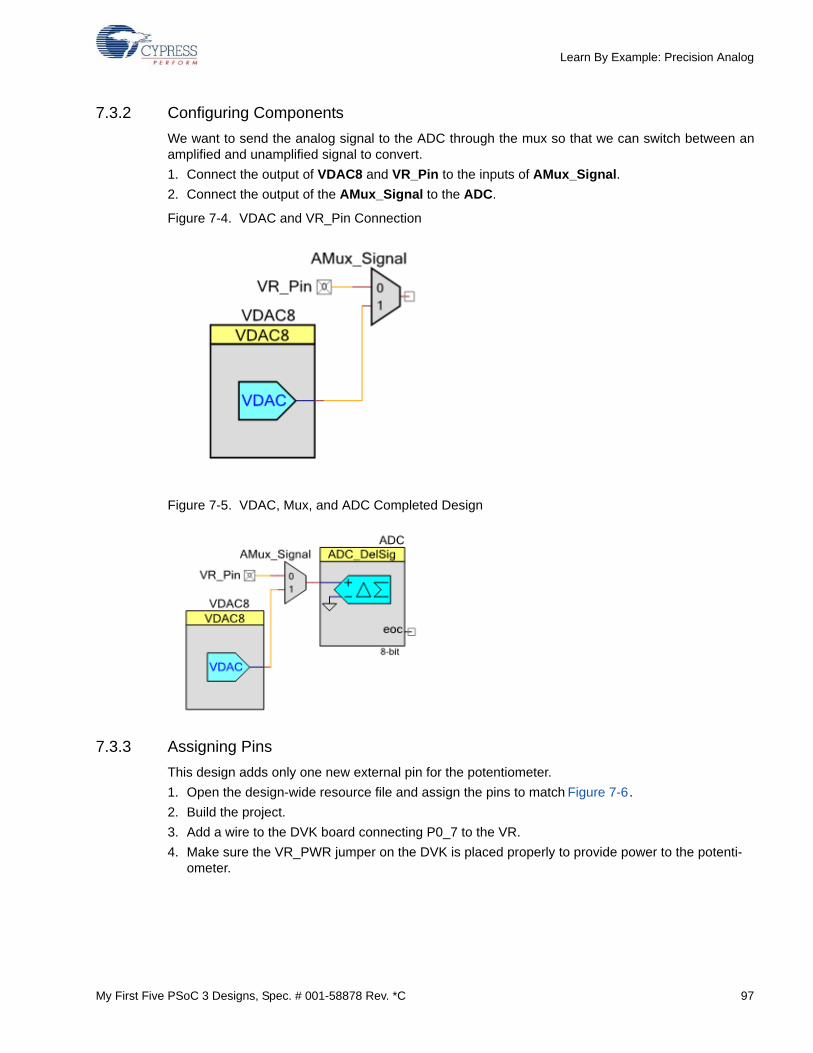
My First Five PSoC 3 Designs, Spec. # 001-58878 Rev. *C 97
Learn By Example: Precision Analog
7.3.2 Configuring Components
We want to send the analog signal to the ADC through the mux so that we can switch between anamplified and unamplified signal to convert.
1. Connect the output of VDAC8 and VR_Pin to the inputs of AMux_Signal.
2. Connect the output of the AMux_Signal to the ADC.
Figure 7-4. VDAC and VR_Pin Connection
Figure 7-5. VDAC, Mux, and ADC Completed Design
7.3.3 Assigning Pins
This design adds only one new external pin for the potentiometer.
1. Open the design-wide resource file and assign the pins to match Figure 7-6.
2. Build the project.
3. Add a wire to the DVK board connecting P0_7 to the VR.
4. Make sure the VR_PWR jumper on the DVK is placed properly to provide power to the potenti-ometer.

98 My First Five PSoC 3 Designs, Spec. # 001-58878 Rev. *C
Learn By Example: Precision Analog
Figure 7-6. Pin Assignments

My First Five PSoC 3 Designs, Spec. # 001-58878 Rev. *C 99
Learn By Example: Precision Analog
7.3.4 Code
1. Make the following changes to the beginning of main.c.
#include "myADC.h"#include "myDAC.h"....................
void main(){ /* Components should be initialized in the following order: * 1. interrupts * 2. sources of interrupts (clocks are auto-initialized) * 3. global interrupt enable */ InitTiming(); /* interrupt */ PWM_Timer_Start(); /* source of interrupt */ InitAdc(); /* source of interrupt */ CYGlobalIntEnable /* macro */
/* Initialize other components, not associated with interrupts */ CharLCD_Start(); InitComPort(); InitCapSense(); InitDac();
..........
2. Add the following lines to the tenth second area of the main loop to call the UpdateCapSense, UpdateAdc, and UpdateDac routines.
3. Comment out the DisplayCount call.
/* This section contains code to be executed every tenth second */if(tenthSecond){ tenthSecond = 0U;
/* Toggle the LED if the button is NOT pressed. This will cause * the LED to blink rapidly when the button is NOT pressed. */ if(Button_Pin_Read()) /* read a 1 when button is NOT pressed */ { ToggleLed(); } UpdateCapSense(); UpdateAdc(); UpdateDac();} /* end of tenth second section */
4. Create a file called myADC.c. Add the following code to the myADC.c file.

100 My First Five PSoC 3 Designs, Spec. # 001-58878 Rev. *C
Learn By Example: Precision Analog
#include <device.h>#include "myADC.h"#include "myDAC.h"
/**************************************** Global Functions***************************************//******************************************************************************** Function Name: InitAdc()*******************************************************************************/void InitAdc(void){ ADC_Start(); ADC_StartConvert(); /* Starts a continuous conversion process */} /* end of InitAdc() */
/******************************************************************************** Function Name: UpdateAdc()*******************************************************************************/void UpdateAdc(void){ if(ADC_IsEndConversion(ADC_RETURN_STATUS)) { uint8 adcval8;
/* Get 14-bit conversion reported in a signed 16-bit result, and limit * negative and positive overflow. */ int16 adcval16 = ADC_GetResult16(); if(adcval16 < 0) { adcval16 = 0; } else if(adcval16 > 0x3FFF) { adcval16 = 0x3FFF; } else {} /* value is in range, do nothing */
/* Convert to an 8-bit result; grab the 8 MS bits. */ adcval8 = (uint8)(((uint16)adcval16 >> 6) & 0xFFU);
/* if reading from the DAC, amplify the reading, because the DAC is * putting out voltage in the range 0 - 1.024V */ if(source != 0U) { adcval8 *= 3U; }
/* display the result on the char LCD */ CharLCD_Position(1U, 6U); /* row, column */ CharLCD_PrintHexUint8(adcval8);
/* Display the result on the UART:
My First Five PSoC 3 Designs, Spec. # 001-58878 Rev. *C 101
Learn By Example: Precision Analog
* Print (val / 4) (with rounding, add half the divisor) 'X' characters, * which creates a horizontal line whose length is proportional to the * ADC value. */ adcval8 = (uint8)(((uint16)adcval8 + 2U) / 4U); if (adcval8 == 0U) /* make sure that at least one 'X' is printed */ { adcval8 = 1U; } for( ; adcval8 != 0U; adcval8--) { UART_1_PutChar('X'); } UART_1_PutString("\r\n"); } /* end of if(ADC_IsEndConversion(ADC_RETURN_STATUS)) */}/* end of UpdateAdc() */
The beginning lines in main routine start the ADC and begin the first conversion. Every 100 millisec-onds, the main loop will check the ADC to see if it has completed its conversion. If the conversionhas completed, it will process and display that conversion result. The next conversion starts auto-matically (continuous conversion mode).
The ADC in this chapter is set to do a 14-bit conversion. The 8 most significant bits are preservedand displayed as an 8-bit result on the LCD screen. The project begins by displaying the letters ADCin the first row of the LCD display with its own conversion result displayed directly below this label.The UpdateAdc routine also sends a string of X characters to the UART. Open a terminal windowwhile running this project to see a simple bar graph representation of the voltage read by the ADC.
1. Create a file called myDAC.c. Add the following code to the myDAC.c file.
#include <device.h>#include "myCapsense.h"#include "myDAC.h"
/**************************************** Global Variables and Macros***************************************/uint8 source = 0U; /* current ADC source, 0 = POT, 1 = DAC */
/**************************************** Private Variables and Macros***************************************//* These variables are used to generate the DAC waveform */static uint8 waveType = 0U; /* which waveform table to use (see below) */static uint8 waveSpeed = 1U; /* how fast to move through the waveform table */
/* data to create sine, sawtooth, triangle and square waves */static uint8 const tables[4][100] ={ { /* sine */ 127U,135U,143U,151U,159U,166U,174U,181U,188U,195U,202U,208U,214U,220U,225U,230U,234U,238U,242U,245U, 248U,250U,252U,253U,254U,254U,254U,253U,252U,250U,248U,245U,242U,238U,234U,230U,225U,220U,214U,208U,
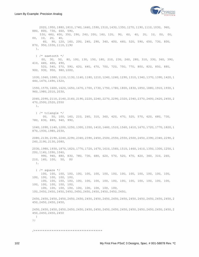
102 My First Five PSoC 3 Designs, Spec. # 001-58878 Rev. *C
Learn By Example: Precision Analog
202U,195U,188U,181U,174U,166U,159U,151U,143U,135U,127U,119U,111U,103U, 96U, 88U, 80U, 73U, 66U, 59U, 53U, 46U, 40U, 35U, 29U, 24U, 20U, 16U, 12U, 9U, 6U, 4U, 2U, 1U, 0U, 0U, 0U, 1U, 2U, 4U, 6U, 9U, 12U, 16U, 20U, 24U, 29U, 34U, 40U, 46U, 52U, 59U, 65U, 73U, 80U, 87U, 95U,103U,111U,119U },
{ /* sawtooth */ 0U, 3U, 5U, 8U, 10U, 13U, 15U, 18U, 21U, 23U, 26U, 28U, 31U, 33U, 36U, 39U, 41U, 44U, 46U, 49U, 52U, 54U, 57U, 59U, 62U, 64U, 67U, 70U, 72U, 75U, 77U, 80U, 82U, 85U, 88U, 90U, 93U, 95U, 98U,100U, 103U,106U,108U,111U,113U,116U,118U,121U,124U,126U,129U,131U,134U,137U,139U,142U,144U,147U,149U,152U, 155U,157U,160U,162U,165U,167U,170U,173U,175U,178U,180U,183U,185U,188U,191U,193U,196U,198U,201U,203U, 206U,209U,211U,214U,216U,219U,222U,224U,227U,229U,232U,234U,237U,240U,242U,245U,247U,250U,252U,255U },
{ /* triangle */ 0U, 5U, 10U, 16U, 21U, 26U, 31U, 36U, 42U, 47U, 52U, 57U, 62U, 68U, 73U, 78U, 83U, 88U, 94U, 99U, 104U,109U,114U,120U,125U,130U,135U,141U,146U,151U,156U,161U,167U,172U,177U,182U,187U,193U,198U,203U, 208U,213U,219U,224U,229U,234U,239U,245U,250U,255U,255U,250U,245U,239U,234U,229U,224U,219U,213U,208U, 203U,198U,193U,187U,182U,177U,172U,167U,161U,156U,151U,146U,141U,135U,130U,125U,120U,114U,109U,104U, 99U, 94U, 88U, 83U, 78U, 73U, 68U, 62U, 57U, 52U, 47U, 42U, 36U, 31U, 26U, 21U, 16U, 10U, 5U, 0U },
{ /* square */ 10U, 10U, 10U, 10U, 10U, 10U, 10U, 10U, 10U, 10U, 10U, 10U, 10U, 10U, 10U, 10U, 10U, 10U, 10U, 10U, 10U, 10U, 10U, 10U, 10U, 10U, 10U, 10U, 10U, 10U, 10U, 10U, 10U, 10U, 10U, 10U, 10U, 10U, 10U, 10U, 10U, 10U, 10U, 10U, 10U, 10U, 10U, 10U, 10U, 10U,245U,245U,245U,245U,245U,245U,245U,245U,245U,245U, 245U,245U,245U,245U,245U,245U,245U,245U,245U,245U,245U,245U,245U,245U,245U,245U,245U,245U,245U,245U, 245U,245U,245U,245U,245U,245U,245U,245U,245U,245U,245U,245U,245U,245U,245U,245U,245U,245U,245U,245U }};
/***************************************

My First Five PSoC 3 Designs, Spec. # 001-58878 Rev. *C 103
Learn By Example: Precision Analog
* Private Functions***************************************//******************************************************************************** Function Name: DisplayDac()********************************************************************************* Summary:* Displays on the char LCD the current state of the analog mux and DAC* waveform generation, including waveform speed.** Parameters:* none** Return:* none********************************************************************************/static void DisplayDac(void){ static char* const msgs[4] = {"SIN", "SAW", "TRI", "SQR"}; /* display current parameters on the char LCD: * analog mux setting, DAC or POT */ CharLCD_Position(0U, 9U); /* row, column */ CharLCD_PrintString(source ? "DAC" : "POT"); /* speed of DAC waveform */ CharLCD_Position(1U, 13U); /* row, column */ CharLCD_PrintInt8(waveSpeed);
/* DAC waveform type (sine, sawtooth, triangle, or square)*/ CharLCD_Position(0U, 13U); /* row, column */ if (waveType >= 4U) /* reset if incorrect value in variable */ { waveType = 0U; } CharLCD_PrintString(msgs[waveType]);} /* end of DisplayDac() */
/**************************************** Global Functions***************************************//******************************************************************************** Function Name: InitDac()*******************************************************************************/void InitDac(void){ AMux_Signal_Start(); AMux_Signal_Select(0U); /* start up looking at the potentiometer */ VDAC8_Start();} /* end of InitDac() */
/******************************************************************************** Function Name: UpdateDac()*******************************************************************************/void UpdateDac(void)

104 My First Five PSoC 3 Designs, Spec. # 001-58878 Rev. *C
Learn By Example: Precision Analog
{ /* initial display flag */ static uint8 init = 1U; /* index into waveform table */ static uint8 index = 0U; /* buttons pressed / released states * [0] = current, [1] = previous * bit 0 is button P0_5, bit 1 is button P0_6 * this is used to detect button unpressed to pressed events */ static uint8 buttons[2] = {0U, 0U}; int8 redisplay = 0; uint8 temp; /* Advance to the next value in the current waveform */ index += waveSpeed; if(index >= 100U) /* handle overflow */ { index -= 100U; } if (waveType > 3U) /* handle incorrect value in variable */ { waveType = 0U; } VDAC8_SetValue((uint8)tables[waveType][index]);
/* update previous then current button values */ buttons[1] = buttons[0]; /* current to previous */ temp = GetButtonP0_5() & 1U; /* buttons to current */ buttons[0] = temp | ((uint8)(GetButtonP0_6() << 1) & 2U); /* CapSense button P0_5 unpressed to pressed changes source */ if(((buttons[1] & 1U) == 0U) && ((buttons[0] & 1U) != 0U)) { source ^= 1U; AMux_Signal_Select(source); redisplay = 1; }
/* CapSense button P0_6 changes waveform type */ if(((buttons[1] & 2U) == 0U) && ((buttons[0] & 2U) != 0U)) { waveType = (waveType + 1U) & 3U; redisplay = 1; }
/* CapSense slider changes waveform speed */ { uint8 myCentroid = GetSlider(); /* translate centroid range 0 - 100 to waveSpeed range 1 - 5 */ if(myCentroid <= 100U) { /* divide with rounding (add (divisor / 2) to dividend before dividing) */ waveSpeed = ((myCentroid + 12U) / 25U) + 1U;

My First Five PSoC 3 Designs, Spec. # 001-58878 Rev. *C 105
Learn By Example: Precision Analog
redisplay = 1; } }
/* Update display if initializing or something changed */ if (init || redisplay) { init = 0U; DisplayDac(); }} /* end of UpdateDac() */
The myDAC.c file indexes into four tables to create wave shapes that resemble a sine wave, saw-tooth wave, triangle wave, and a square wave. The CapSense button P0_5 controls the mux andswitches between the potentiometer and the DAC as a signal source. Successive presses on buttonP0_6 switch the DAC wave generation from the sine wave to the saw tooth, to the triangle, to thesquare wave, and back to the sine wave. The speed of the wave varies from 1 to 5x, and is con-trolled with the slider. The type of wave and speed of the wave being sent to the DAC are displayedon the LCD display.
Create a new header file for your project called myADC.h and add the following content to that file.Include this file in main.c.
*****************************************************************************/
/******************************************************************************** Function Name: InitAdc()********************************************************************************* Summary:* Initializes the ADC component and starts conversions.** Parameters:* none** Return:* none********************************************************************************/void InitAdc(void);
/******************************************************************************** Function Name: UpdateAdc()********************************************************************************* Summary:* Does one A/D conversion and displays the result on the Char LCD and the* UART.** Parameters:* none** Return:* none********************************************************************************/void UpdateAdc(void);/* [] END OF FILE */

106 My First Five PSoC 3 Designs, Spec. # 001-58878 Rev. *C
Learn By Example: Precision Analog
Create a new header file for your project called myDAC.h and add the following content to that file.Include this file in main.c.
/******************************************************************************** Function Name: InitDac()********************************************************************************* Summary:* Initializes the analog mux and DAC components, and starts generating a* default waveform.** Parameters:* none** Return:* none********************************************************************************/void InitDac(void);
/******************************************************************************** Function Name: UpdateDac()********************************************************************************* Summary:* Checks the CapSense controls and updates the DAC waveform generation.** Parameters:* none** Return:* none********************************************************************************/void UpdateDac(void);
/**************************************** Global Variables***************************************/extern uint8 source; /* current ADC source, 0 = POT, 1 = DAC */
7.4 Conclusion
The PSoC device keeps the analog processing inside the microcontroller where it is more immune tooutside noise influences. The precision analog links with the digital resources to provide an interwo-ven system inside a single chip.
Set up the components within your project before you start the PCB layout of the project. Make surethe routing you need is possible after adding all the components to your schematic view. Note that ifyou can alter your PCB to match the suggested pin assignments from PSoC Creator, you will be ableto fit the most components and functionality into your design.
The PSoC platform allows you to add external components to the design that interact with internalanalog to achieve custom gain and filter processing in the analog domain. Keep the power requiredby the internal components to a minimum to guarantee the best accuracy. Experiment with differentpower settings with the analog components. Power settings have tradeoffs in speed and power.They may also have a slight effect on settling and accuracy.
My First Five PSoC 3 Designs, Spec. # 001-58878 Rev. *C 107
Learn By Example: Precision Analog
7.5 Additional Information
Make sure to study the TRM and data sheet to understand the architecture of the analog systems inthe PSoC device. Do not be discouraged if your analog project does not route correctly the first timeor if it seems impossible to get the analog setup that you need for your project.
When developing a system that is particularly difficult or atypical, there is a tendency to give up tooearly and decide that the design is not feasible. The PSoC system is flexible enough that it is verylikely there are some other approaches to your design that you have not thought of. Take some timeto consider all possible options. If the design requirements are not typical, then the best solution verywell may not be typical. I have worked on many designs that I did not think would work at the begin-ning with PSoC microcontrollers and then found a way later after some experimentation and persis-tence.
There may be a bit of frustration when you cannot probe inside the chip to find out what is happeningwith analog signals. It is good practice to leave a test point on your PCB to serve as a test outputpoint. Simply connect the point in question to this output point during development to measure whatis happening at that particular stage.
When you are developing more complex designs, the number of items in the schematic may make itimpossible to route the analog port components to any combination of pins that you want. In this sit-uation it is best to first add your components and build the project without locking any analog or digi-tal components to specific pins. PSoC Creator will optimize the routing inside the chip and suggestthe best pins to use according to its algorithms. After it has built successfully with the freedom toassign pins, start with the pins that are most needed to be in specific locations and assign a few ofthem to the desired I/O pins and rebuild the project.
If you do this a few pins at a time, you will have a better idea where the conflict is compared to lock-ing all the pins in a particular location and then wondering why PSoC Creator cannot route the proj-ect successfully.

108 My First Five PSoC 3 Designs, Spec. # 001-58878 Rev. *C
Learn By Example: Precision Analog

My First Five PSoC 3 Designs, Spec. # 001-58878 Rev. *C 109
Index
Numerics8051 CPU 15
AADC 93, 101
sigma delta 8, 15, 95adding a new project 42, 60, 73adding a register 74, 79adding components 25, 43, 61, 93advanced high performance bus 7AHB See advanced high performance busanalog mux 94analog port 93, 107analog reference 93analog resources 71analog system 8, 93, 107AnimateBoat function 83application notes 70architecture
PSoC 3 and PSoC 5 7PSoC platform 7
assigning pins 30, 49, 66, 97
Bbaseline 60, 62, 66baud rate 41, 58bit rate 50, 58blinking an LED 23–40
continual repeating blink 38using a counter 39
buffer 48, 82Build/Debug toolbar 37building a project 29, 37, 55button component 37
CCAN 15capacitive sensing 59, 70CapSense 17, 59–71CapSense_1 component 61CapSense_CSD component 61central processing unit See CPUcharacter LCD 43
Character LCD component 60CharLCD component 44, 70clock 25, 49clock input 79clock_PWM component 25, 26, 49clocking structure 51code 31, 51, 67, 81, 99COM port 41, 47, 57command 83comparator 15Component Catalog 25, 95Components tab 20comport.h 51, 53Configure dialog 25Configure System Clocks dialog 51configuring a register 74configuring a UART 41–58configuring clocks 49configuring components 61, 97connecting components 28content and organization 5control register 74, 79, 90conventions 13CPU 6, 48, 90
8051 15creating a new schematic page 73cydwr file 19, 30, 43, 49
DD Flip Flop 79DAC 8, 16
current 8voltage 8, 93, 94
data integrity 50Data Sheet button 26datapath 10debounce 60, 62Debug menu 37debugging a project 37, 55design practices 70design-wide resources 21, 66
file 30, 43, 97DFB See digital filter blockdigital filter block 8digital logic 73–91digital output pin 28

110 My First Five PSoC 3 Designs, Spec. # 001-58878 Rev. *C
Index
digital port 29digital to analog converter See DACdisplay.c 43display.h 43DisplayCount function 44, 82, 99DisplayWelcome function 44DMA controller 8document
revision history 13dPort_Button component 29DVK1 board 17, 30, 34, 37, 41, 56, 59, 64, 66
Eembedded system 6error checking 80error detection 50example designs
organization 22ExecuteRiddle function 83external clock 47external crystal 51
FfarmerRiddle.c 81farmerRiddle.h 81finger threshold 60, 62, 63firmware 61, 62, 70flag 23flow control 47
Ggesturing 59global interrupt flag 34GPIO 16
Hhardware delay 79header files 22headers 30Hyperterminal 54hysteresis 60, 62
II/O logic 34IMO 49initialization 34InitializeAllBaselines routine 67InitRiddle function 82, 83internal clock 47, 51internal logic 30internal main oscillator See IMO
interrupt 29, 48intializeComPort function 54isr_PWM component 29, 34isr_PWM.c 37
Jjumpers 17
Llayout guidelines 70LCD 16, 41, 45, 63, 70, 82, 83, 101LCD_Char_1 component 43LED 23, 28
blinking 23–40, 45, 56continual repeating blink 38using a counter 39
ledEnabled 54LEDPin 56linear slider 62liquid crystal display See LCDlogic component 73lookup table See LUTLUT 73, 78, 79, 80, 94
Mmain.c 31, 34, 38, 44, 53, 69, 81, 99Master Clock 51memory 6
EEPROM 7Flash 6RAM 7, 48
microcontrollers 6, 106microprocessor 7MiniProg3 17multiplexer 30multi-touch 59myADC.c 99myCapsense.c 67, 70myCapsense.h 68myDAC.c 101, 105
Nnoise 93noise floor 93noise immunity 93noise threshold 60, 62, 63, 66non return to zero See NRZ communicationNRZ communication 57
Oopamp 8, 15

My First Five PSoC 3 Designs, Spec. # 001-58878 Rev. *C 111
Index
operational amplifier See opampoutput latches 34Output window 25oversampling 47, 50
Pparity bit 47PCB 30, 59, 93
layout 106period 23, 27, 38periodic interrupt 38periodic task management 23peripheral hub 7peripherals 7PHUB See peripheral hubPLD 9potentiometer 93power settings 106precision analog 93–107prototyping area 30proximity detection 59PS register 34PSoC 3 and PSoC 5 architecture 7PSoC Creator 18
Component Catalog 25Configure dialog 25Debug menu 37Output window 25schematic view 21Start Page 18, 24View menu 25Workspace Explorer 19, 25
PSoC platform 5, 7, 93, 106architecture 7
PWM 23, 26, 38PWM_Pin 54, 56PWM_Timer component 27, 28, 54
RRAM 7, 48Results tab 20revision history 13routing 30, 93, 106, 107RS232 41, 57, 58
Ssawtooth wave 105SC/CT block 8, 15schematic 29, 49, 73, 79, 107schematic view 21sensor design 70serial communication device 41, 57serial port connector 56sheet connector 75, 79
sigma delta ADC 8, 15, 95sine wave 105slider 59
linear 63source files 22Source tab 19start bit 41start function 31Start Page 18, 24starting a new project 24state machine 73, 79status register 74, 79, 80, 90stop bit 41, 47super I/O chip 57SW1 button 34, 37, 38, 45switched cap 8
Ttenth second area 44, 82, 99tenthSecondDelay function 83Tera Term 54terminal program 54terminal window 101TestRiddle function 82, 83timing flag 38timing system 23timing.c 34, 83timing.h 44toggleLED function 34, 54
UUART 41–58, 101
Mark state 57Space state 57
UART_1 component 49, 50, 54, 83UDB 15, 90
array 11See also universal digital block
universal digital block 8UpdateAdc function 99, 101UpdateComPort function 54, 82UpdateDac function 99UpdateRiddle function 82, 83USB 15, 41, 57USB to RS232 converter 41USB to UART bridge 41USB2UART component 41
VVerilog 15View menu 25

112 My First Five PSoC 3 Designs, Spec. # 001-58878 Rev. *C
Index
Wwave shapes 105Workspace Explorer 19, 25
Components tab 20Results tab 20Source tab 19
Related Documents