© KEMET Electronics Corporation, P.O. Box 5928, Greenville, S.C. 29606, (864) 963-6300 4 MULTILAYER CERAMIC CAPACITORS/AXIAL & RADIAL LEADED Multilayer ceramic capacitors are available in a variety of physical sizes and configurations, including leaded devices and surface mounted chips. Leaded styles include molded and conformally coated parts with axial and radial leads. However, the basic capacitor element is similar for all styles. It is called a chip and consists of formulated dielectric materials which have been cast into thin layers, interspersed with metal electrodes alternately exposed on opposite edges of the laminated structure. The entire structure is fired at high temperature to produce a monolithic block which provides high capacitance values in a small physical volume. After firing, conductive terminations are applied to opposite ends of the chip to make contact with the exposed electrodes. Termination materials and methods vary depending on the intended use. TEMPERATURE CHARACTERISTICS Ceramic dielectric materials can be formulated with a wide range of characteristics. The EIA standard for ceramic dielectric capacitors (RS-198) divides ceramic dielectrics into the following classes: Class I: Temperature compensating capacitors, suitable for resonant circuit application or other appli- cations where high Q and stability of capacitance char- acteristics are required. Class I capacitors have predictable temperature coefficients and are not affected by voltage, frequency or time. They are made from materials which are not ferro-electric, yielding superior stability but low volumetric efficiency. Class I capacitors are the most stable type available, but have the lowest volumetric efficiency. Class II: Stable capacitors, suitable for bypass or coupling applications or frequency discriminating circuits where Q and stability of capacitance char- acteristics are not of major importance. Class II capacitors have temperature characteristics of ± 15% or less. They are made from materials which are ferro-electric, yielding higher volumetric efficiency but less stability. Class II capacitors are affected by temperature, voltage, frequency and time. Class III: General purpose capacitors, suitable for by-pass coupling or other applications in which dielectric losses, high insulation resistance and stability of capacitance characteristics are of little or no importance. Class III capacitors are similar to Class II capacitors except for temperature characteristics, which are greater than ± 15%. Class III capacitors have the highest volumetric efficiency and poorest stability of any type. KEMET leaded ceramic capacitors are offered in the three most popular temperature characteristics: C0G: Class I, with a temperature coefficient of 0 ± 30 ppm per degree C over an operating temperature range of - 55°C to + 125°C (Also known as “NP0”). X7R: Class II, with a maximum capacitance change of ± 15% over an operating temperature range of - 55°C to + 125°C. Z5U: Class III, with a maximum capacitance change of + 22% - 56% over an operating tem- perature range of + 10°C to + 85°C. Specified electrical limits for these three temperature characteristics are shown in Table 1. SPECIFIED ELECTRICAL LIMITS Table I C0G X7R Z5U Dissipation Factor: Measured at following conditions. C0G – 1 kHz and 1 vrms if capacitance >1000pF 1 MHz and 1 vrms if capacitance 1000 pF X7R – 1 kHz and 1 vrms* or if extended cap range 0.5 vrms Z5U – 1 kHz and 0.5 vrms 0.10% 2.5% (3.5% @ 25V) 4.0% Dielectric Stength: 2.5 times rated DC voltage. Insulation Resistance (IR): At rated DC voltage, whichever of the two is smaller 1,000 M F or 100 G 1,000 M F or 100 G 1,000 M F or 10 G Temperature Characteristics: Range, °C Capacitance Change without DC voltage -55 to +125 0 ± 30 ppm/°C -55 to +125 ± 15% + 10 to +85 +22%,-56% * MHz and 1 vrms if capacitance 100 pF on military product. Parameter Temperature Characteristics Pass Subsequent IR Test

Welcome message from author
This document is posted to help you gain knowledge. Please leave a comment to let me know what you think about it! Share it to your friends and learn new things together.
Transcript

© KEMET Electronics Corporation, P.O. Box 5928, Greenville, S.C. 29606, (864) 963-63004
MULTILAYER CERAMIC CAPACITORS/AXIAL & RADIAL LEADED
Multilayer ceramic capacitors are available in avariety of physical sizes and configurations, includingleaded devices and surface mounted chips. Leadedstyles include molded and conformally coated partswith axial and radial leads. However, the basiccapacitor element is similar for all styles. It is called achip and consists of formulated dielectric materialswhich have been cast into thin layers, interspersedwith metal electrodes alternately exposed on opposite
edges of the laminated structure. The entire structure isfired at high temperature to produce a monolithicblock which provides high capacitance values in asmall physical volume. After firing, conductiveterminations are applied to opposite ends of the chip tomake contact with the exposed electrodes.Termination materials and methods vary depending onthe intended use.
TEMPERATURE CHARACTERISTICSCeramic dielectric materials can be formulated with
a wide range of characteristics. The EIA standard forceramic dielectric capacitors (RS-198) divides ceramicdielectrics into the following classes:
Class I: Temperature compensating capacitors,suitable for resonant circuit application or other appli-cations where high Q and stability of capacitance char-acteristics are required. Class I capacitors havepredictable temperature coefficients and are notaffected by voltage, frequency or time. They are madefrom materials which are not ferro-electric, yieldingsuperior stability but low volumetric efficiency. Class Icapacitors are the most stable type available, but havethe lowest volumetric efficiency.
Class II: Stable capacitors, suitable for bypassor coupling applications or frequency discriminatingcircuits where Q and stability of capacitance char-acteristics are not of major importance. Class IIcapacitors have temperature characteristics of ± 15%or less. They are made from materials which areferro-electric, yielding higher volumetric efficiency butless stability. Class II capacitors are affected bytemperature, voltage, frequency and time.
Class III: General purpose capacitors, suitablefor by-pass coupling or other applications in whichdielectric losses, high insulation resistance andstability of capacitance characteristics are of little orno importance. Class III capacitors are similar to ClassII capacitors except for temperature characteristics,which are greater than ± 15%. Class III capacitorshave the highest volumetric efficiency and pooreststability of any type.
KEMET leaded ceramic capacitors are offered inthe three most popular temperature characteristics:
C0G: Class I, with a temperature coefficient of 0 ±30 ppm per degree C over an operatingtemperature range of - 55°C to + 125°C (Alsoknown as “NP0”).X7R: Class II, with a maximum capacitancechange of ± 15% over an operating temperaturerange of - 55°C to + 125°C.Z5U: Class III, with a maximum capacitancechange of + 22% - 56% over an operating tem-perature range of + 10°C to + 85°C.
Specified electrical limits for these three temperaturecharacteristics are shown in Table 1.
SPECIFIED ELECTRICAL LIMITS
Table I
C0G X7R Z5U
Dissipation Factor: Measured at following conditions.C0G – 1 kHz and 1 vrms if capacitance >1000pF
1 MHz and 1 vrms if capacitance 1000 pFX7R – 1 kHz and 1 vrms* or if extended cap range 0.5 vrmsZ5U – 1 kHz and 0.5 vrms
0.10% 2.5%(3.5% @ 25V) 4.0%
Dielectric Stength: 2.5 times rated DC voltage.
Insulation Resistance (IR): At rated DC voltage,whichever of the two is smaller
1,000 M For 100 G
1,000 M For 100 G
1,000 M For 10 G
Temperature Characteristics: Range, °CCapacitance Change withoutDC voltage
-55 to +1250 ± 30 ppm/°C
-55 to +125± 15%
+ 10 to +85+22%,-56%
* MHz and 1 vrms if capacitance 100 pF on military product.
Parameter Temperature Characteristics
Pass Subsequent IR Test
ELECTRICAL CHARACTERISTICS
The fundamental electrical properties of multilayerceramic capacitors are as follows:
Polarity: Multilayer ceramic capacitors are not polar,and may be used with DC voltage applied in either direction.
Rated Voltage: This term refers to the maximum con-tinuous DC working voltage permissible across the entireoperating temperature range. Multilayer ceramic capacitorsare not extremely sensitive to voltage, and brief applicationsof voltage above rated will not result in immediate failure.However, reliability will be reduced by exposure to sustainedvoltages above rated.
Capacitance: The standard unit of capacitance is thefarad. For practical capacitors, it is usually expressed inmicrofarads (10-6 farad), nanofarads (10-9 farad), or picofarads(10-12 farad). Standard measurement conditions are asfollows:
Class I (up to 1,000 pF): 1MHz and 1.2 VRMSmaximum.
Class I (over 1,000 pF): 1kHz and 1.2 VRMSmaximum.
Class II: 1 kHz and 1.0 ± 0.2 VRMS.
Class III: 1 kHz and 0.5 ± 0.1 VRMS.
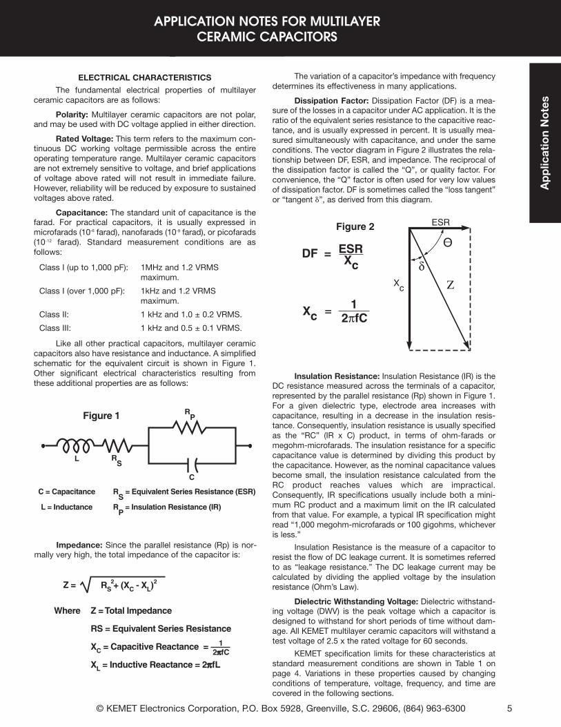
Like all other practical capacitors, multilayer ceramiccapacitors also have resistance and inductance. A simplifiedschematic for the equivalent circuit is shown in Figure 1.Other significant electrical characteristics resulting fromthese additional properties are as follows:
Impedance: Since the parallel resistance (Rp) is nor-mally very high, the total impedance of the capacitor is:
Figure 1
C = Capacitance
L = Inductance
RS
= Equivalent Series Resistance (ESR)
RP
= Insulation Resistance (IR)
RP
RS
C
L
Z =
Where Z = Total Impedance
RS = Equivalent Series Resistance
XC = Capacitive Reactance = 2ππfC
XL = Inductive Reactance = 2ππfL
1
RS + (XC - XL)2 2
DF = ESRXc
Xc 2πfC1=
Figure 2
δΖ
O
Xc
ESR
The variation of a capacitor’s impedance with frequencydetermines its effectiveness in many applications.
Dissipation Factor: Dissipation Factor (DF) is a mea-sure of the losses in a capacitor under AC application. It is theratio of the equivalent series resistance to the capacitive reac-tance, and is usually expressed in percent. It is usually mea-sured simultaneously with capacitance, and under the sameconditions. The vector diagram in Figure 2 illustrates the rela-tionship between DF, ESR, and impedance. The reciprocal ofthe dissipation factor is called the “Q”, or quality factor. Forconvenience, the “Q” factor is often used for very low valuesof dissipation factor. DF is sometimes called the “loss tangent”or “tangent d”, as derived from this diagram.
Insulation Resistance: Insulation Resistance (IR) is theDC resistance measured across the terminals of a capacitor,represented by the parallel resistance (Rp) shown in Figure 1.For a given dielectric type, electrode area increases withcapacitance, resulting in a decrease in the insulation resis-tance. Consequently, insulation resistance is usually specifiedas the “RC” (IR x C) product, in terms of ohm-farads ormegohm-microfarads. The insulation resistance for a specificcapacitance value is determined by dividing this product bythe capacitance. However, as the nominal capacitance valuesbecome small, the insulation resistance calculated from theRC product reaches values which are impractical.Consequently, IR specifications usually include both a mini-mum RC product and a maximum limit on the IR calculatedfrom that value. For example, a typical IR specification mightread “1,000 megohm-microfarads or 100 gigohms, whicheveris less.”
Insulation Resistance is the measure of a capacitor toresist the flow of DC leakage current. It is sometimes referredto as “leakage resistance.” The DC leakage current may becalculated by dividing the applied voltage by the insulationresistance (Ohm’s Law).
Dielectric Withstanding Voltage: Dielectric withstand-ing voltage (DWV) is the peak voltage which a capacitor isdesigned to withstand for short periods of time without dam-age. All KEMET multilayer ceramic capacitors will withstand atest voltage of 2.5 x the rated voltage for 60 seconds.
KEMET specification limits for these characteristics atstandard measurement conditions are shown in Table 1 onpage 4. Variations in these properties caused by changingconditions of temperature, voltage, frequency, and time arecovered in the following sections.
© KEMET Electronics Corporation, P.O. Box 5928, Greenville, S.C. 29606, (864) 963-6300 5
APPLICATION NOTES FOR MULTILAYERCERAMIC CAPACITORS
Ap
plic
atio
nN
ote
s

APPLICATION NOTES FOR MULTILAYER CERAMIC CAPACITORS
© KEMET Electronics Corporation, P.O. Box 5928, Greenville, S.C. 29606, (864) 963-63006
TABLE 1EIA TEMPERATURE CHARACTERISTIC CODES
FOR CLASS I DIELECTRICS
Significant Figure Multiplier Applied Tolerance ofof Temperature to Temperature Temperature
Coefficient Coefficient Coefficient *
PPM per Letter Multi- Number PPM per LetterDegree C Symbol plier Symbol Degree C Symbol
0.0 C -1 0 ±30 G0.3 B -10 1 ±60 H0.9 A -100 2 ±120 J1.0 M -1000 3 ±250 K1.5 P -100000 4 ±500 L2.2 R +1 5 ±1000 M3.3 S +10 6 ±2500 N4.7 T +100 77.5 U +1000 8
+10000 9* These symetrical tolerances apply to a two-point measurement oftemperature coefficient: one at 25°C and one at 85°C. Some deviationis permitted at lower temperatures. For example, the PPM tolerancefor C0G at -55°C is +30 / -72 PPM.
TABLE 2EIA TEMPERATURE CHARACTERISTIC CODES
FOR CLASS II & III DIELECTRICS
Low Temperature High Temperature Maximum CapacitanceRating Rating Shift
Degree Letter Degree Number LetterCelcius Symbol Celcius Symbol Percent Symbol
+10C Z +45C 2 ±1.0% A-30C Y +65C 4 ±1.5% B-55C X +85C 5 ±2.2% C
+105C 6 ±3.3% D+125C 7 ±4.7% E+150C 8 ±7.5% F+200C 9 ±10.0% P
±15.0% R±22.0% S
+22/-33% T+22/-56% U+22/-82% V
+10 +20 +30 +40 +50 +60 +70 +80

Effect of Temperature: Both capacitance and dissipa-tion factor are affected by variations in temperature. The max-imum capacitance change with temperature is defined by thetemperature characteristic. However, this only defines a “box”bounded by the upper and lower operating temperatures andthe minimum and maximum capacitance values. Within this“box”, the variation with temperature depends upon the spe-cific dielectric formulation. Typical curves for KEMET capaci-tors are shown in Figures 3, 4, and 5. These figures alsoinclude the typical change in dissipation factor for KEMETcapacitors.
Insulation resistance decreases with temperature.Typically, the insulation resistance at maximum rated temper-ature is 10% of the 25°C value.
Effect of Voltage: Class I ceramic capacitors are notaffected by variations in applied AC or DC voltages. For ClassII and III ceramic capacitors, variations in voltage affect onlythe capacitance and dissipation factor. The application of DCvoltage higher than 5 vdc reduces both the capacitance anddissipation factor. The application of AC voltages up to 10-20Vac tends to increase both capacitance and dissipation factor.
At higher AC voltages, both capacitance and dissipation factorbegin to decrease.
Typical curves showing the effect of applied AC and DCvoltage are shown in Figure 6 for KEMET X7R capacitors andFigure 7 for KEMET Z5U capacitors.
Effect of Frequency: Frequency affects both capaci-tance and dissipation factor. Typical curves for KEMET multi-layer ceramic capacitors are shown in Figures 8 and 9.
The variation of impedance with frequency is an impor-tant consideration in the application of multilayer ceramiccapacitors. Total impedance of the capacitor is the vector of thecapacitive reactance, the inductive reactance, and the ESR, asillustrated in Figure 2. As frequency increases, the capacitivereactance decreases. However, the series inductance (L)shown in Figure 1 produces inductive reactance, whichincreases with frequency. At some frequency, the impedanceceases to be capacitive and becomes inductive. This point, atthe bottom of the V-shaped impedance versus frequencycurves, is the self-resonant frequency. At the self-resonant fre-quency, the reactance is zero, and the impedance consists ofthe ESR only.
Typical impedance versus frequency curves for KEMETmultilayer ceramic capacitors are shown in Figures 10, 11, and12. These curves apply to KEMET capacitors in chip form, with-out leads. Lead configuration and lead length have a significantimpact on the series inductance. The lead inductance isapproximately 10nH/inch, which is large compared to theinductance of the chip. The effect of this additional inductanceis a decrease in the self-resonant frequency, and an increasein impedance in the inductive region above the self-resonantfrequency.
Effect of Time: The capacitance of Class II and IIIdielectrics change with time as well as with temperature, volt-age and frequency. This change with time is known as “aging.”It is caused by gradual realignment of the crystalline structureof the ceramic dielectric material as it is cooled below its Curietemperature, which produces a loss of capacitance with time.The aging process is predictable and follows a logarithmicdecay. Typical aging rates for C0G, X7R, and Z5U dielectrics are as follows:
C0G NoneX7R 2.0% per decade of timeZ5U 5.0% per decade of time
Typical aging curves for X7R and Z5U dielectrics areshown in Figure 13.
The aging process is reversible. If the capacitor is heat-ed to a temperature above its Curie point for some period oftime, de-aging will occur and the capacitor will regain thecapacitance lost during the aging process. The amount of de-aging depends on both the elevated temperature and thelength of time at that temperature. Exposure to 150°C for one-half hour or 125°C for two hours is usually sufficient to returnthe capacitor to its initial value.
Because the capacitance changes rapidly immediatelyafter de-aging, capacitance measurements are usually delayedfor at least 10 hours after the de-aging process, which is oftenreferred to as the “last heat.” In addition, manufacturers utilizethe aging rates to set factory test limits which will bring thecapacitance within the specified tolerance at some future time,to allow for customer receipt and use. Typically, the test limitsare adjusted so that the capacitance will be within the specifiedtolerance after either 1,000 hours or 100 days, depending onthe manufacturer and the product type.
© KEMET Electronics Corporation, P.O. Box 5928, Greenville, S.C. 29606, (864) 963-6300 7
Ap
plic
atio
nN
ote
s
APPLICATION NOTES FOR MULTILAYER CERAMIC CAPACITORS

APPLICATION NOTES FOR MULTILAYER CERAMIC CAPACITORS
© KEMET Electronics Corporation, P.O. Box 5928, Greenville, S.C. 29606, (864) 963-63008
POWER DISSIPATIONPower dissipation has been empirically determined for
two representative KEMET series: C052 and C062. Power dis-sipation capability for various mounting configurations is shownin Table 3. This table was extracted from Engineering BulletinF-2013, which provides a more detailed treatment of this sub-ject.
Note that no significant difference was detected betweenthe two sizes in spite of a 2 to 1 surface area ratio. Due to thematerials used in the construction of multilayer ceramic capac-itors, the power dissipation capability does not depend greatlyon the surface area of the capacitor body, but rather on howwell heat is conducted out of the capacitor lead wires.Consequently, this power dissipation capability is applicable toother leaded multilayer styles and sizes.
TABLE 3POWER DISSIPATION CAPABILITY(Rise in Celsius degrees per Watt)
PowerMounting Configuration Dissipation
of C052 & C062
1.00" leadwires attached to binding post 90 Celsius degreesof GR-1615 bridge (excellent heat sink) rise per Watt ±10%
0.25" leadwires attached to binding post 55 Celsius degreesof GR-1615 bridge rise per Watt ±10%
Capacitor mounted flush to 0.062" glass- 77 Celsius degreesepoxy circuit board with small copper traces rise per Watt ±10%
Capacitor mounted flush to 0.062" glass- 53 Celsius degreesepoxy circuit board with four square inches rise per Watt ±10%of copper land area as a heat sink
As shown in Table 3, the power dissipation capability ofthe capacitor is very sensitive to the details of its use environ-ment. The temperature rise due to power dissipation should notexceed 20°C. Using that constraint, the maximum permissiblepower dissipation may be calculated from the data provided inTable 3.
It is often convenient to translate power dissipation capa-bility into a permissible AC voltage rating. Assuming a sinu-soidal wave form, the RMS “ripple voltage” may be calculated
The data necessary to make this calculation is included inEngineering Bulletin F-2013. However, the following criteriamust be observed:
1. The temperature rise due to power dissipationshould be limited to 20°C.
2. The peak AC voltage plus the DC voltage must notexceed the maximum working voltage of thecapacitor.
Provided that these criteria are met, multilayer ceramic
E = Z x
Where E = RMS Ripple Voltage (volts)
P = Power Dissipation (watts)
Z = Impedance
R = ESR
PMAXR
capacitors may be operated with AC voltage applied withoutneed for DC bias.
RELIABILITYA well constructed multilayer ceramic capacitor is
extremely reliable and, for all practical purposes, has an infi-nite life span when used within the maximum voltage andtemperature ratings. Capacitor failure may be induced by sus-tained operation at voltages that exceed the rated DC voltage,voltage spikes or transients that exceed the dielectric with-standing voltage, sustained operation at temperatures abovethe maximum rated temperature, or the excessive tempera-ture rise due to power dissipation.
Failure rate is usually expressed in terms of percent per1,000 hours or in FITS (failure per billion hours). SomeKEMET series are qualified under U.S. military establishedreliability specifications MIL-PRF-20, MIL-PRF-123, MIL-PRF-39014, and MIL-PRF-55681. Failure rates as low as0.001% per 1,000 hours are available for all capacitance /voltage ratings covered by these specifications. These spec-ifications and accompanying Qualified Products List shouldbe consulted for details.
For series not covered by these military specifications,an internal testing program is maintained by KEMET QualityAssurance. Samples from each week’s production are sub-jected to a 2,000 hour accelerated life test at 2 x rated voltageand maximum rated temperature. Based on the results ofthese tests, the average failure rate for all non-military seriescovered by this test program is currently 0.06% per 1,000hours at maximum rated conditions. The failure rate would bemuch lower at typical use conditions. For example, using MIL-HDBK-217D this failure rate translates to 0.9 FITS at 50%rated voltage and 50°C.
Current failure rate details for specific KEMET multilay-er ceramic capacitor series are available on request.
MISAPPLICATIONCeramic capacitors, like any other capacitors, may fail
if they are misapplied. Typical misapplications include expo-sure to excessive voltage, current or temperature. If thedielectric layer of the capacitor is damaged by misapplicationthe electrical energy of the circuit can be released as heat,which may damage the circuit board and other componentsas well.
If potential for misapplication exists, it is recommendedthat precautions be taken to protect personnel and equipmentduring initial application of voltage. Commonly used precau-tions include shielding of personnel and sensing for excessivepower drain during board testing.
STORAGE AND HANDLINGCeramic chip capacitors should be stored in normal
working environments. While the chips themselves are quiterobust in other environments, solderability will be degradedby exposure to high temperatures, high humidity, corrosiveatmospheres, and long term storage. In addition, packagingmaterials will be degraded by high temperature – reels maysoften or warp, and tape peel force may increase. KEMETrecommends that maximum storage temperature not exceed40˚ C, and maximum storage humidity not exceed 70% rela-tive humidity. In addition, temperature fluctuations should beminimized to avoid condensation on the parts, and atmos-pheres should be free of chlorine and sulfur bearing com-pounds. For optimized solderability, chip stock should beused promptly, preferably within 1.5 years of receipt.
from the following formula:

IMPEDANCE VS FREQUENCY
Imp
edan
ce(O
hm
s)
1 10 100 1,0000.001
0.01
1
10
100
0.1
0.1
Frequency - MHzImpedance vs Frequency for C0G Dielectric
Figure 10.
EFFECT OF FREQUENCY
-0.1
0
+0.2
-0.2
+0.1
0.10
0.20
0.0
Frequency - HertzCapacitance & DF vs Frequency - C0G
Figure 8.
%D
F
Typical Aging Rates for X7R & Z5UFigure 13.
74%76%78%80%82%84%86%88%90%92%94%96%98%
100%
Cap
acit
ance
1 10 100 1000 10K 100K
EFFECT OF TIME
%D
F
-10
-5
+5
-15
0
5.0
10.0
0.0
2.5
7.5
Frequency - HertzCapacitance & DF vs Frequency - X7R & Z5U
Figure 9.
.01μF .001μF
%Δ
C
100 1K 10K 100K 1M 10M
100 1K 10K 100K 1M 10M
%Δ
C %ΔC
%DF
Z5U
X7R
%DF
%ΔC
Imp
edan
ce(O
hm
s)
1 10 100 1,0000.001
0.01
1
10
100
0.1
0.1
Frequency - MHzImpedance vs Frequency for Z5U Dielectric
Figure 12.
Imp
edan
ce(O
hm
s)
1 10 100 1,0000.001
0.01
1
10
100
0.1
0.1
Frequency - MHzImpedance vs Frequency for X7R Dielectric
Figure 11.
0.1μF
1.0 μF
0.1μF .01μF
1.0 μF
Impedance vs. Frequency
Leaded Ceramic C0G
0.01
0.1
1
10
100
0.1 1 1 0 100 1000
Frequency - MHz
Imp
ed
an
ce
(Oh
ms
)
0.01µF
0.001µF
Leaded X7R
0.01
0.1
1
10
100
0.1 1 1 0 100 1000
Frequency - MHz
Imp
ed
an
ce
(Oh
ms)
0.01µF
0.1µF
Impedance vs. Frequency
1.0µF
Impedance vs. FrequencyLeaded Z5U
0.01
0.1
1
10
100
0.1 1 1 0 100 1000
Frequency - MHz
Imp
ed
an
ce
(Oh
ms)
0.1µF
1.0µF
Impedance vs Frequencyfor C0G Dielectric
Figure 10.
Impedance vs Frequencyfor Z5U Dielectric
Figure 12.
Impedance vs Frequencyfor X7R Dielectric
Figure 11.
Impedance vs Frequencyfor C0G Dielectric
Figure 10.
Impedance vs Frequencyfor Z5U Dielectric
Figure 12.
Impedance vs Frequencyfor X7R Dielectric
Figure 11.
Impedance vs Frequencyfor C0G Dielectric
Figure 10.
Impedance vs Frequencyfor Z5U Dielectric
Figure 12.
Impedance vs Frequencyfor X7R Dielectric
Figure 11.
���
�����
���
�
� ������������� ������������� �������
���
���
� �
© KEMET Electronics Corporation, P.O. Box 5928, Greenville, S.C. 29606, (864) 963-6300 9
Ap
plic
atio
nN
ote
s
APPLICATION NOTES FOR MULTILAYER CERAMIC CAPACITORS
Impedance vs Frequencyfor C0G Dielectric
Figure 10.
Impedance vs Frequencyfor Z5U Dielectric
Figure 12.
Impedance vs Frequencyfor X7R Dielectric
Figure 11.
Impedance vs Frequencyfor C0G Dielectric
Figure 10.
Impedance vs Frequencyfor Z5U Dielectric
Figure 12.
Impedance vs Frequencyfor X7R Dielectric
Figure 11.
Impedance vs Frequencyfor C0G Dielectric
Figure 10.
Impedance vs Frequencyfor Z5U Dielectric
Figure 12.
Impedance vs Frequencyfor X7R Dielectric
Figure 11.
(hours)

© KEMET Electronics Corporation, P.O. Box 5928, Greenville, S.C. 29606, (864) 963-630040
CERAMIC MOLDED/MIL-C-11015 & MIL-PRF-39014 (CKR)
C062 (CK06, CKR06)
Lead Dia..025
(+.004-.002)
W
.026MIN.
H
L
S
W
.045MAX.
H
1.25MIN.
L
S
W
H
1.25MIN.
L
S
W
Center Line of leads within .030" of Center Line of case.
H
1.25MIN.
S
.026MIN.
L
C052 (CK05, CKR05) C056 (CKR05) C066 (CKR06)
Lead Dia..025
(+.004-.002)
Lead Dia..025
(+.004-.002)
Lead Dia..025
(+.004-.002)
1.25MIN.* *
* *
DIMENSIONS — INCHES (MILLIMETERS)
DL
C
1.50 Min.(38.10)
1.50 Min.(38.10)
CAPACITOR OUTLINE DRAWINGS - (AXIAL LEADS)CAPACITOR OUTLINE DRAWINGS (AXIAL LEADS)
CAPACITOR OUTLINE DRAWINGS (RADIAL LEADS)
DIMENSIONS — INCHES (MILLIMETERS)
* Leads are .625 minimum when tape and reel packaged.
CaseSize
MilitaryEquivalent Styles
LLength
DBody Diameter
CLead Diameter
C114 CK12, CKR11 .160 ± .010 (4.06 ± .25) .090 ± .010 (2.29 ± .25) .020, +.000, -.003 (.51, +.00, -.08)
C124 CK13, CCR12 .250 ± .010 (6.35 ± .25) .090 ± .010 (2.29 ± .25) .020, +.000, -.003 (.51, +.00, -.08)
C192 CK14, CKR14 .390 ± .010 (9.91 ± .25) .140 ± .010 (3.56 ± .25) .025, +.002, -.002 (.64, +.05, -.05)
C202 CK15, CKR15 .500 ± .020 (12.70 ± .51) .250 ± .015 (6.35 ± .38) .025, +.002, -.002 (.64, +.05, -.05)
C222 CK16, CKR16 .690 ± .030 (17.53 ± .76) .350 ± .020 (8.89 ± .51) .025, +.002, -.002 (.64, +.05, -.05)
Case
Size
Military
Equivalent Styles
H
Height
L
Length
W
Width
S
Lead
Spacing
C052/
C056CK05, CKR05 .190 ± .010 (4.83 ± .25) .190 ± .010 (4.83 ± .25) .090 ± .010 (2.29 ± .25) .200 ± .015 (5.08 ± .38)
C062/
C066CK06, CKR06 .290 ± .010 (7.37 ± .25) .290 ± .010 (7.37 ± .25) .090 ± .010 (2.29 ± .25) .200 ± .015 (5.08 ± .38)

© KEMET Electronics Corporation, P.O. Box 5928, Greenville, S.C. 29606, (864) 963-6300 41
C114T (CKR11)
ORDERING INFORMATION
MARKING INFORMATIONC114T (CKR11) THROUGH C222T (CKR16) PER MIL-PRF-39014
JK
103KP837A
J for JANK for KEMETCapacitanceCapacitance Tolerance, FR Level& Date Code (Year)Week and Lot Code
C124T (CKR12)CKR12
2657J
0837A
31433
StyleDash No., J for JAN
Date & Lot CodeSource Code(Federal Supply Codefor Manufacturers,FSCM)
C192T (CKR14) C202T (CKR15) C222T (CKR16)M39014
5-2125
KEMET
0837A
J50V
105K
Complete Part NumberManufacturer’s Name
Date & Lot CodeJAN & Voltage
Capacitance, pF Code, CapacitanceTolerance
C052/56T (CKR05) PER MIL-PRF-39014/01
JK
0837
A
JAN-KEMETDate Code
Lot Code
BACK
M390
14/01
1579*
Specification
Sheet No.Four Digit Part No.*Add “V” as the lastdigit for stand-off leads.
FRONT
C062/66T (CKR06) PER MIL-PRF-39014/02
0837A
J200V
103K
Date & Lot CodeJAN & Voltage
Capacitance, pF Code, Capacitance Tolerance
BACK
M39014
2-1338
*KEMET
Complete MIL Part No.
Manufacturer’s Name
FRONT
*Add “V” as the last digitfor stand-off leads.
C114K (CK12) THROUGH C222K (CK16) PER MIL-C-11015C114K (CK12) C124K (CK13)
KCK12BX102K0837
KEMET, CKStyle (12 or 13), Temp. Char. (BX or BR)Capacitance, pF Code, Capacitance ToleranceDate Code
C192K (CK14) C202K (CK15) C222K (CK16)K100V
CK14BX123K0837
KEMET, VoltageStyle (14, 15 or 16), Temp. Char. (BX or BR)Capacitance, pF Code, Capacitance ToleranceDate Code
C052K (CK05) PER MIL-C-11015/18 & C062K (CK06) PER MIL-C-11015/19
200VK
0801
VoltageKEMET
Date Code
BACK
CK05BX102K
StyleTemperature Characteristic
Capacitance, pF Code, Capacitance Tolerance
FRONT
C 052 K 102 K 2 X 5 C ACERAMICCASE SIZESee Table Below
SPECIFICATIONMilitaryT – MIL-PRF-39014K – MIL-C-11015CAPACITANCE PICOFARAD CODEExpressed in picofarads (pF). First two digits representsignificant figures. Third digit specifies number of zerosfollowing except 9 indicates division by 10). Examples:0.1 µF = 100,000 pF = 104 and 9.1 pF = 919. Seetables for standard values.
CAPACITANCE TOLERANCEM – ±20%K – ±10%
WORKING VOLTAGE DC2 – 200V; 1 – 100V; 5 – 50V
FAILURE RATEA – Not ApplicableM – 1.0%P – 0.1%R – 0.01%S – 0.001%
INTERNAL CONSTRUCTION5 – Multilayer
TEMPERATURE CHARACTERISTIC
KEMETDesignator
MilitaryEquivalent
EIAEquivalent
Cap. Change with Temp.
TempRange, °C
Measuredwithout DC
Bias Voltage
Measuredwith Bias
(RatedVoltage)
X(Stable) BX X7R -55 to
+125° ±15% +15%-25%
R(Stable) BR X7R -55° to
+125 ±15% +15%-40%
Standard tolerances for each Seriesare shown in the repetitive parts lists.
Case SizesRadial AxialC052 C114C056 C124C062 C192C066 C202
C222Part Number Example: C052K102K2X5CA (14 digits – no spaces)
MIL
-C-1
1015
MIL
-PR
F-39
014
CERAMIC MOLDED/MIL-C-11015 & MIL-PRF-39014 (CKR)
LEAD MATERIALC – 60/40 Tin/Lead (SnPb)

© KEMET Electronics Corporation, P.O. Box 5928, Greenville, S.C. 29606, (864) 963-630042
CERAMIC MOLDED/AXIAL — MIL-C-11015 & MIL-PRF-39014
STABLE TEMPERATURE CHARACTERISTICS—BX & BR (EIA-X7R)
RATINGS & PART NUMBER REFERENCE
(1) Insert proper letter for specification: K — MIL-C-11015; T — MIL-PRF-39014 (2) Failure Rate Designator: A — Not applicable (MIL-C-11015); M — 1%/1000 Hours,P — .1%/1000 Hours, R — .01%/1000 Hours, S — .001%/1000 Hours (MIL-PRF-39014)
M P R S
10 10 C114(1)100K1X5C(2) CK12BX100K CKR11BX100K(2) 2601 2801 2001 2201
10 20 C114(1)100M1X5C(2) CK12BX100M CKR11BX100M(2) 2602 2802 2002 2202
12 10 C114(1)120K1X5C(2) CK12BX120K CKR11BX120K(2) 2603 2803 2003 2203
15 10 C114(1)150K1X5C(2) CK12BX120K CKR11BX150K(2) 2604 2804 2004 2204
15 20 C114(1)150M1X5C(2) CK12BX150M CKR11BX150M(2) 2605 2805 2005 2205
18 10 C114(1)180K1X5C(2) CK12BX180K CKR11BX180K(2) 2606 2806 2006 2206
22 10 C114(1)220K1X5C(2) CK12BX220K CKR11BX220K(2) 2607 2807 2007 2207
22 20 C114(1)220M1X5C(2) CK12BX220M CKR11BX220M(2) 2608 2808 2008 2208
27 10 C114(1)270K1X5C(2) CK12BX270K CKR11BX270K(2) 2609 2809 2009 2209
33 10 C114(1)330K1X5C(2) CK12BX330K CKR11BX330K(2) 2610 2810 2010 2210
33 20 C114(1)330M1X5C(2) CK12BX330M CKR11BX330M(2) 2611 2811 2011 2211
39 10 C114(1)390K1X5C(2) CK12BX390K CKR11BX390K(2) 2612 2812 2012 2212
47 10 C114(1)470K1X5C(2) CK12BX470K CKR11BX470K(2) 2613 2813 2013 2213
47 20 C114(1)470M1X5C(2) CK12BX470M CKR11BX470M(2) 2614 2814 2014 2214
56 10 C114(1)560K1X5C(2) CK12BX560K CKR11BX560K(2) 2615 2815 2015 2215
68 10 C114(1)680K1X5C(2) CK12BX680K CKR11BX560K(2) 2616 2816 2016 2216
68 20 C114(1)680M1X5C(2) CK12BX680M CKR11BX680M(2) 2617 2817 2017 2217
82 10 C114(1)820K1X5C(2) CK12BX820K CKR11BX820K(2) 2618 2818 2018 2218
100 10 C114(1)101K1X5C(2) CK12BX102K CKR11BX102K(2) 2619 2819 2019 2219
100 20 C114(1)101M1X5C(2) CK12BX102M CKR11BX102M(2) 2620 2820 2020 2220
120 10 C114(1)121K1X5C(2) CK12BX121K CKR11BX121K(2) 2621 2821 2021 2221
150 10 C114(1)151K1X5C(2) CK12BX151K CKR11BX151K(2) 2622 2822 2022 2222
150 20 C114(1)151M1X5C(2) CK12BX151M CKR11BX151M(2) 2623 2823 2023 2223
180 10 C114(1)181K1X5C(2) CK12BX181K CKR11BX181K(2) 2624 2824 2024 2224
220 10 C114(1)221K1X5C(2) CK12BX221K CKR11BX221K(2) 2625 2825 2025 2225
220 20 C114(1)221M1X5C(2) CK12BX221M CKR11BX221K(2) 2626 2826 2026 2226
270 10 C114(1)271K1X5C(2) CK12BX271K CKR11BX271K(2) 2627 2827 2027 2227
330 10 C114(1)331K1X5C(2) CK12BX331K CKR11BX331K(2) 2628 2828 2028 2228
330 20 C114(1)331M1X5C(2) CK12BX331M CKR11BX331M(2) 2629 2829 2029 2229
390 10 C114(1)391K1X5C(2) CK12BX391K CKR11BX391K(2) 2630 2830 2030 2230
470 10 C114(1)471K1X5C(2) CK12BX471K CKR11BX471K(2) 2631 2831 2031 2231
470 20 C114(1)471M1X5C(2) CK12BX471M CKR11BX471M(2) 2632 2832 2032 2232
560 10 C114(1)561K1X5C(2) CK12BX561K CKR11BX561K(2) 2633 2833 2033 2233
680 10 C114(1)681K1X5C(2) CK12BX681K CKR11BX561K(2) 2634 2834 2034 2234
680 20 C114(1)681M1X5C(2) CK12BX681M CKR11BX681M(2) 2635 2835 2035 2235
820 10 C114(1)821K1X5C(2) CK12BX821K CKR11BX821K(2) 2636 2836 2036 2236
1,000 10 C114(1)102K1X5C(2) CK12BX102K CKR11BX102K(2) 2637 2837 2037 2237
1,000 20 C114(1)102M1X5C(2) CK12BX102M CKR11BX102M(2) 2638 2838 2038 2238
1,200 10 C114(1)122K1X5C(2) CK12BX122K CKR11BX122K(2) 2639 2839 2039 2239
1,500 10 C114(1)152K1X5C(2) CK12BX152K CKR11BX152K(2) 2640 2840 2040 2240
1,500 20 C114(1)152M1X5C(2) CK12BX152M CKR11BX152M(2) 2641 2841 2041 2241
1,800 10 C114(1)182K1X5C(2) CK12BX182K CKR11BX182K(2) 2642 2842 2042 2242
2,200 10 C114(1)222K1X5C(2) CK12BX222K CKR11BX222K(2) 2643 2843 2043 2243
2,200 20 C114(1)222M1X5C(2) CK12BX222M CKR11BX222M(2) 2644 2844 2044 2244
2,700 10 C114(1)272K1X5C(2) CK12BX272K CKR11BX272K(2) 2645 2845 2045 2245
3,300 10 C114(1)332K1X5C(2) CK12BX332K CKR11BX332K(2) 2646 2846 2046 2246
3,300 20 C114(1)332M1X5C(2) CK12BX332M CKR11BX332M(2) 2647 2847 2047 2247
3,900 10 C114(1)392K1X5C(2) CK12BX392K CKR11BX392K(2) 2648 2848 2048 2248
4,700 10 C114(1)472K1X5C(2) CK12BX472K CKR11BX472K(2) 2649 2849 2049 2249
4,700 20 C114(1)472M1X5C(2) CK12BX472M CKR11BX472M(2) 2650 2850 2050 2250
5,600 10 C114(1)562K5X5C(2) CK12BX562K CKR11BX562K(2) 2651 2851 2051 2251
6,800 10 C114(1)682K5X5C(2) CK12BX682K CKR11BX682K(2) 2652 2852 2052 2252
6,800 20 C114(1)682M5X5C(2) CK12BX682M CKR11BX682M(2) 2653 2853 2053 2253
8,200 10 C114(1)822K5X5C(2) CK12BX822K CKR11BX822K(2) 2654 2854 2054 2254
10,000 10 C114(1)103K5X5C(2) CK12BX103K CKR11BX103K(2) 2655 2855 2055 2255
10,000 20 C114(1)103M5X5C(2) CK12BX103M CKR11BX103M(2) 2656 2856 2056 2256
5,600 10 C124(1)562K1X5C(2) CK13BX562K CKR12BX562K(2) 2657 2857 2057 2257
6,800 10 C124(1)682K1X5C(2) CK13BX682K CKR12BX682K(2) 2658 2858 2058 2258
6,800 20 C124(1)682M1X5C(2) CK13BX682M CKR12BX682M(2) 2659 2859 2059 2259
8,200 10 C124(1)822K1X5C(2) CK13BX822K CKR12BX822K(2) 2660 2860 2060 2260
10,000 10 C124(1)103K1X5C(2) CK13BX103K CKR12BX103K(2) 2661 2861 2061 2261
10,000 20 C124(1)103M1X5C(2) CK13BX103M CKR12BX103M(2) 2662 2862 2062 2262
12,000 10 C124(1)123K5X5C(2) CK13BX123K CKR12BX123K(2) 2663 2863 2063 2263
15,000 10 C124(1)153K5X5C(2) CK13BX153K CKR12BX153K(2) 2664 2864 2064 2264
15,000 20 C124(1)153M5X5C(2) CK13BX153M CKR12BX153M(2) 2665 2865 2065 2265
18,000 10 C124(1)183K5X5C(2) CK13BX183K CKR12BX183K(2) 2666 2866 2066 2266
22,000 10 C124(1)183K5X5C(2) CK13BX223K CKR12BX223K(2) 2667 2861 2061 2261
22,000 20 C124(1)223M5X5C(2) CK13BX223M CKR12BX223M(2) 2668 2868 2068 2268
27,000 10 C124(1)273K5X5C(2) CK13BX273K
33,000 10 C124(1)333K5X5C(2) CK13BX333K
33,000 20 C124(1)333M5X5C(2) CK13BX333M
39,000 10 C124(1)393K5X5C(2) CK13BX393K
47,000 10 C124(1)473K5X5C(2) CK13BX473K
47,000 20 C124(1)473M5X5C(2) CK13BX473M
50 VOLT – C114 SIZE (MILITARY-CK12 or CKR11)
100 VOLT – C124 SIZE (MILITARY-CK13 or CKR12)
50 VOLT – C124 SIZE (MILITARY-CK13 or CKR12)
MIL-PRF-39014/05 For Failure
Rate Levels (2)
100 VOLT – C114 SIZE (MILITARY-CK12 or CKR11)
CAP.
pF
TOL.
%
KEMET
PART NUMBERMIL-C-11015/02 MIL-PRF-39014/05

© KEMET Electronics Corporation, P.O. Box 5928, Greenville, S.C. 29606, (864) 963-6300 43
RATINGS & PART NUMBER REFERENCE
(1) Insert proper letter for specification: K — MIL-C-11015; T — MIL-PRF-39014 (2) Failure Rate Designator: A — Not applicable (MIL-C-11015); M — 1%/1000 Hours,P — .1%/1000 Hours, R — .01%/1000 Hours, S — .001%/1000 Hours (MIL-PRF-39014)
MIL
-C-1
1015
MIL
-PR
F-39
014
CERAMIC MOLDED/AXIAL — MIL-C-11015 & MIL-PRF-39014
STABLE TEMPERATURE CHARACTERISTICS—BX & BR (EIA-X7R)
M P R S
27,000 10 C124T273K5X5C(2) CKR12BX273K(2) 2669 2869 2069 226933,000 10 C124T333K5X5C(2) CKR12BX333K(2) 2670 2870 2070 227033,000 20 C124T333M5X5C(2) CKR12BX333M(2) 2671 2871 2071 227139,000 10 C124T393K5X5C(2) CKR12BX393K(2) 2672 2872 2072 227247,000 10 C124T473K5X5C(2) CKR12BX473K(2) 2673 2873 2073 227347,000 20 C124T473M5X5C(2) CKR12BX473M(2) 2674 2874 2074 2274
12,000 10 C192(1)123K1X5C(2) CK14BX123K CKR14BX123K(2) 2675 2875 2075 227515,000 10 C192(1)153K1X5C(2) CK14BX153K CKR14BX153K(2) 2676 2876 2076 227615,000 20 C192(1)153M1X5C(2) CK14BX153M CKR14BX153M(2) 2677 2877 2077 227718,000 10 C192(1)183K1X5C(2) CK14BX183K CKR14BX183K(2) 2678 2878 2078 227822,000 10 C192(1)223K1X5C(2) CK14BX223K CKR14BX223K(2) 2679 2879 2079 227922,000 20 C192(1)223M1X5C(2) CK14BX223M CKR14BX223M(2) 2680 2880 2080 228027,000 10 C192(1)273K1X5C(2) CK14BX273K CKR14BX273K(2) 2681 2881 2081 228133,000 10 C192(1)333K1X5C(2) CK14BX333K CKR14BX333K(2) 2682 2882 2082 228233,000 20 C192(1)333M1X5C(2) CK14BX333M CKR14BX333M(2) 2683 2883 2083 228339,000 10 C192(1)393K1X5C(2) CK14BX393K CKR14BX393K(2) 2684 2884 2084 228447,000 10 C192(1)473K1X5C(2) CK14BX473K CKR14BX473K(2) 2685 2885 2085 228547,000 20 C192(1)473M1X5C(2) CK14BX473M CKR14BX473M(2) 2686 2886 2086 228656,000 10 C192(1)563K1X5C(2) CK14BR563K CKR14BR563K(2) 2693 2893 2093 229368,000 10 C192(1)683K1X5C(2) CK14BR683K CKR14BR683K(2) 2694 2894 2094 229468,000 20 C192(1)683M1X5C(2) CK14BR683M CKR14BR683M(2) 2695 2895 2095 229582,000 10 C192(1)823K1X5C(2) CK14BR823K CKR14BR823K(2) 2696 2896 2096 2296100,000 10 C192(1)104K1X5C(2) CK14BR104K CKR14BR104K(2) 2697 2897 2097 2297100,000 20 C192(1)104M1X5C(2) CK14BR104M CKR14BR104M(2) 2698 2898 2098 2298
56,000 10 C192T563K5X5C(2) CKR14BX563K(2) 2687 2887 2087 228768,000 10 C192T683K5X5C(2) CKR14BX683K(2) 2688 2888 2088 228868,000 20 C192T683M5X5C(2) CKR14BX683M(2) 2689 2889 2089 228982,000 10 C192T823K5X5C(2) CKR14BX823K(2) 2690 2890 2090 2290100,000 10 C192T104K5X5C(2) CKR14BX104K(2) 2691 2891 2091 2291100,000 20 C192T104M5X5C(2) CKR14BX104M(2) 2692 2892 2092 2292120,000 10 C192(1)124K5X5C(2) CK14BR124K CKR14BX124K(2) 2699 2899 2099 2299150,000 10 C192(1)154K5X5C(2) CK14BR154K CKR14BX154K(2) 2700 2900 2100 2300150,000 20 C192(1)154M5X5C(2) CK14BR154M CKR14BX154M(2) 2701 2901 2101 2301180,000 10 C192(1)184K5X5C(2) CK14BR184K CKR14BX184K(2) 2702 2902 2102 2302220,000 10 C192(1)224K5X5C(2) CK14BR224K CKR14BX224K(2) 2703 2903 2103 2303220,000 20 C192(1)224M5X5C(2) CK14BR224M CKR14BX224M(2) 2704 2904 2104 2304270,000 10 C192(1)274K5X5C(2) CK14BR274K CKR14BX274K(2) 2705 2905 2105 2305
56,000 10 C202T563K1X5C(2) CKR15BX563K(2) 2706 2906 2106 230668,000 10 C202T683K1X5C(2) CKR15BX683K(2) 2707 2907 2107 230768,000 20 C202T683M1X5C(2) CKR15BX683K(2) 2708 2908 2108 230882,000 10 C202T823K1X5C(2) CKR15BX823K(2) 2709 2909 2109 2309100,000 10 C202(1)104K1X5C(2) CK15BX104K CKR15BX104K(2) 2710 2910 2110 2310100,000 20 C202(1)104M1X5C(2) CK15BX104M CKR15BX104M(2) 2711 2911 2111 2311120,000 10 C202(1)124K1R5C(2) CK15BR124K CKR15BR124K(2) 2712 2912 2112 2312150,000 10 C202(1)154K1R5C(2) CK15BR154K CKR15BR154K(2) 2713 2913 2113 2313150,000 20 C202(1)154M1R5C(2) CK15BR154M CKR15BR154M(2) 2714 2914 2114 2314180,000 10 C202(1)184K1R5C(2) CK15BR184K CKR15BR184K(2) 2715 2915 2115 2315220,000 10 C202(1)224K1R5C(2) CK15BR224K CKR15BR224K(2) 2716 2916 2116 2316220,000 20 C202(1)224M1R5C(2) CK15BR224M CKR15BR224M(2) 2717 2917 2117 2317270,000 10 C202(1)274K1R5C(2) CK15BR274K CKR15BR274K(2) 2718 2918 2118 2318330,000 10 C202(1)334K1R5C(2) CK15BR334K CKR15BR334K(2) 2719 2919 2119 2319330,000 20 C202(1)334M1R5C(2) CK15BR334M CKR15BR334M(2) 2720 2920 2120 2320
470,000 10 C202(1)474K5R5C(2) CK15BR474K CKR15BR474K(2) 2721 2921 2121 2321470,000 20 C202(1)474M5R5C(2) CK15BR474M CKR15BR474M(2) 2722 2922 2122 2322680,000 10 C202T684K5R5C(2) CKR15BR684K(2) 2723 2923 2123 2323680,000 20 C202T684M5R5C(2) CKR15BR684M(2) 2724 2924 2124 2324
1,000,000 10 C202(1)105K5R5C(2) CK15BR105K CKR15BR105K(2) 2725 2925 2125 23251,000,000 20 C202(1)105M5R5C(2) CK15BR105M CKR15BR105M(2) 2726 2926 2126 2326
470,000 10 C222(1)474K1R5C(2) CK16BR474K CKR16BR474K(2) 2727 2927 2127 2327470,000 20 C222(1)474M1R5C(2) CK16BR474M CKR16BR474M(2) 2728 2928 2128 2328680,000 10 C222(1)684K1R5C(2) CKR16BR684K(2) 2729 2929 2129 2329680,000 20 C222(1)684M1R5C(2) CKR16BR684M(2) 2730 2930 2130 2330
1,000,000 10 C222(1)105K1R5C(2) CK16BR105K CKR16BR105K(2) 2731 2931 2131 23311,000,000 20 C222(1)105M1R5C(2) CK16BR105M CKR16BR105M(2) 2732 2932 2132 2332
2,200,000 10 C222(1)225K5R5C(2) CK16BR225K CKR16BR225K(2) 2733 2933 2133 23332,200,000 20 C222(1)225M5R5C(2) CK16BR225M CKR16BR225M(2) 2734 2934 2134 23343,300,000 10 C222(1)335K5R5C(2) CK16BR335K CKR16BR335K(2) 2735 2935 2135 23353,300,000 20 C222(1)335M5R5C(2) CK16BR335M CKR16BR335M(2) 2736 2936 2136 2336
100 VOLT – C192 SIZE (MILITARY-CK14 or CKR14)
50 VOLT – C192 SIZE (MILITARY-CK14 or CKR14)
50 VOLT – C222 SIZE (MILITARY-CK16 or CKR16)
100 VOLT – C222 SIZE (MILITARY-CK16 or CKR16)
100 VOLT – C202 SIZE (MILITARY-CK15 or CKR15)
50 VOLT – C202 SIZE (MILITARY-CK15 or CKR15)
MIL-PRF-39014/05 For FailureRate Levels (2)
50 VOLT – C124 SIZE (MILITARY-CK13 or CKR12)(continued)
CAP.pF
TOL.%
KEMETPART NUMBER MIL-C-11015/02 MIL-PRF-39014/05

© KEMET Electronics Corporation, P.O. Box 5928, Greenville, S.C. 29606, (864) 963-630044
CERAMIC MOLDED/RADIAL — MIL-C-11015 & MIL-PRF-39014
STABLE TEMPERATURE CHARACTERISTICS—BX & BR (EIA-X7R)
(1) Insert proper letter for specification: K — MIL-C-11015; T — MIL-PRF-39014 (2) Failure Rate Designator: A — Not applicable (MIL-C-11015); M — 1%/1000 Hours,P — .1%/1000 Hours, R — .01%/1000 Hours, S — .001%/1000 Hours (MIL-PRF-39014)(3) Insert “V” for standard design (C056). Leave blank for the flat bottom design (C052).(4) Insert “2” for standard design (Style C052) Note: Stand-offs are available only
Insert “6” for stand-off design (Style C056) with the CKR, not the CK.}
RATINGS & PART NUMBER REFERENCE
M P R S
10 10 C05(4)(1)100K2X5C(2) CK05BX100K CKR05BX100K(2)(3) 1201(3) 1241(3) 1281(3) 1321(3)
10 20 C05(4)(1)100M2X5C(2) CK05BX100M CKR05BX100M(2)(3) 1202(3) 1242(3) 1282(3) 1322(3)
12 10 C05(4)(1)120K2X5C(2) CK05BX120K CKR05BX120K(2)(3) 1203(3) 1243(3) 1283(3) 1323(3)
15 10 C05(4)(1)150K2X5C(2) CK05BX150K CKR05BX150K(2)(3) 1204(3) 1244(3) 1284(3) 1324(3)
15 20 C05(4)(1)150M2X5C(2) CK05BX150M CKR05BX150M(2)(3) 1205(3) 1245(3) 1285(3) 1325(3)
18 10 C05(4)(1)180K2X5C(2) CK05BX180K CKR05BX180K(2)(3) 1206(3) 1246(3) 1286(3) 1326(3)
22 10 C05(4)(1)220K2X5C(2) CK05BX220K CKR05BX220K(2)(3) 1207(3) 1247(3) 1287(3) 1327(3)
22 20 C05(4)(1)220M2X5C(2) CK05BX220M CKR05BX220M(2)(3) 1208(3) 1248(3) 1288(3) 1328(3)
27 10 C05(4)(1)270K2X5C(2) CK05BX270K CKR05BX270K(2)(3) 1209(3) 1249(3) 1289(3) 1329(3)
33 10 C05(4)(1)330K2X5C(2) CK05BX330K CKR05BX330K(2)(3) 1210(3) 1250(3) 1290(3) 1330(3)
33 20 C05(4)(1)330M2X5C(2) CK05BX330M CKR05BX330M(2)(3) 1211(3) 1251(3) 1291(3) 1331(3)
39 10 C05(4)(1)390K2X5C(2) CK05BX390K CKR05BX390K(2)(3) 1212(3) 1252(3) 1292(3) 1332(3)
47 10 C05(4)(1)470K2X5C(2) CK05BX470K CKR05BX470K(2)(3) 1213(3) 1253(3) 1293(3) 1333(3)
47 20 C05(4)(1)470M2X5C(2) CK05BX470M CKR05BX470M(2)(3) 1214(3) 1254(3) 1294(3) 1334(3)
56 10 C05(4)(1)560K2X5C(2) CK05BX560K CKR05BX560K(2)(3) 1215(3) 1255(3) 1295(3) 1335(3)
68 10 C05(4)(1)680K2X5C(2) CK05BX680K CKR05BX680K(2)(3) 1216(3) 1256(3) 1296(3) 1336(3)
68 20 C05(4)(1)680M2X5C(2) CK05BX680M CKR05BX680M(2)(3) 1217(3) 1257(3) 1297(3) 1337(3)
82 10 C05(4)(1)820K2X5C(2) CK05BX820K CKR05BX820K(2)(3) 1218(3) 1258(3) 1298(3) 1338(3)
100 10 C05(4)(1)101K2X5C(2) CK05BX101K CKR05BX101K(2)(3) 1219(3) 1259(3) 1299(3) 1339(3)
100 20 C05(4)(1)101M2X5C(2) CK05BX101M CKR05BX101M(2)(3) 1220(3) 1260(3) 1300(3) 1340(3)
120 10 C05(4)(1)121K2X5C(2) CK05BX121K CKR05BX121K(2)(3) 1221(3) 1261(3) 1301(3) 1341(3)
150 10 C05(4)(1)151K2X5C(2) CK05BX151K CKR05BX151K(2)(3) 1222(3) 1262(3) 1302(3) 1342(3)
150 20 C05(4)(1)151M2X5C(2) CK05BX151M CKR05BX151M(2)(3) 1223(3) 1263(3) 1303(3) 1343(3)
180 10 C05(4)(1)181K2X5C(2) CK05BX181K CKR05BX181K(2)(3) 1224(3) 1264(3) 1304(3) 1344(3)
220 10 C05(4)(1)221K2X5C(2) CK05BX221K CKR05BX221K(2)(3) 1225(3) 1265(3) 1305(3) 1345(3)
220 20 C05(4)(1)221M2X5C(2) CK05BX221M CKR05BX221M(2)(3) 1226(3) 1266(3) 1306(3) 1346(3)
270 10 C05(4)(1)271K2X5C(2) CK05BX271K CKR05BX271K(2)(3) 1227(3) 1267(3) 1307(3) 1347(3)
330 10 C05(4)(1)331K2X5C(2) CK05BX331K CKR05BX331K(2)(3) 1228(3) 1268(3) 1308(3) 1348(3)
330 20 C05(4)(1)331M2X5C(2) CK05BX331M CKR05BX331M(2)(3) 1229(3) 1269(3) 1309(3) 1349(3)
390 10 C05(4)(1)391K2X5C(2) CK05BX391K CKR05BX391K(2)(3) 1230(3) 1270(3) 1310(3) 1350(3)
470 10 C05(4)(1)471K2X5C(2) CK05BX471K CKR05BX471K(2)(3) 1231(3) 1271(3) 1311(3) 1351(3)
470 20 C05(4)(1)471M2X5C(2) CK05BX471M CKR05BX471M(2)(3) 1232(3) 1272(3) 1312(3) 1352(3)
560 10 C05(4)(1)561K2X5C(2) CK05BX561K CKR05BX561K(2)(3) 1233(3) 1273(3) 1313(3) 1353(3)
680 10 C05(4)(1)681K2X5C(2) CK05BX681K CKR05BX681K(2)(3) 1234(3) 1274(3) 1314(3) 1354(3)
680 20 C05(4)(1)681M2X5C(2) CK05BX681M CKR05BX681M(2)(3) 1235(3) 1275(3) 1315(3) 1355(3)
820 10 C05(4)(1)821K2X5C(2) CK05BX821K CKR05BX821K(2)(3) 1236(3) 1276(3) 1316(3) 1356(3)
1,000 10 C05(4)(1)102K2X5C(2) CK05BX102K CKR05BX102K(2)(3) 1237(3) 1277(3) 1317(3) 1357(3)
1,000 20 C05(4)(1)102M2X5C(2) CK05BX102M CKR05BX102M(2)(3) 1238(3) 1278(3) 1318(3) 1358(3)
1,200 10 C05(4)(1)122K1X5C(2) CK05BX122K CKR05BX122K(2)(3) 1239(3) 1279(3) 1319(3) 1359(3)
1,500 10 C05(4)(1)152K1X5C(2) CK05BX152K CKR05BX152K(2)(3) 1240(3) 1280(3) 1320(3) 1360(3)
1,500 20 C05(4)(1)152M1X5C(2) CK05BX152M CKR05BX152M(2)(3) 1441(3) 1481(3) 1521(3) 1561(3)
1,800 10 C05(4)(1)182K1X5C(2) CK05BX182K CKR05BX182K(2)(3) 1442(3) 1482(3) 1522(3) 1562(3)
2,200 10 C05(4)(1)222K1X5C(2) CK05BX222K CKR05BX222K(2)(3) 1443(3) 1483(3) 1523(3) 1563(3)
2,200 20 C05(4)(1)222M1X5C(2) CK05BX222M CKR05BX222M(2)(3) 1444(3) 1484(3) 1524(3) 1564(3)
2,700 10 C05(4)(1)272K1X5C(2) CK05BX272K CKR05BX272K(2)(3) 1445(3) 1485(3) 1525(3) 1565(3)
3,300 10 C05(4)(1)332K1X5C(2) CK05BX332K CKR05BX332K(2)(3) 1446(3) 1486(3) 1526(3) 1566(3)
3,300 20 C05(4)(1)332M1X5C(2) CK05BX332M CKR05BX332M(2)(3) 1447(3) 1487(3) 1527(3) 1567(3)
3,900 10 C05(4)(1)392K1X5C(2) CK05BX392K CKR05BX392K(2)(3) 1448(3) 1488(3) 1528(3) 1568(3)
4,700 10 C05(4)(1)472K1X5C(2) CK05BX472K CKR05BX472K(2)(3) 1449(3) 1489(3) 1529(3) 1569(3)
4,700 20 C05(4)(1)472M1X5C(2) CK05BX472M CKR05BX472M(2)(3) 1450(3) 1490(3) 1530(3) 1570(3)
5,600 10 C05(4)(1)562K1X5C(2) CK05BX562K CKR05BX562K(2)(3) 1451(3) 1491(3) 1531(3) 1571(3)
6,800 10 C05(4)(1)682K1X5C(2) CK05BX682K CKR05BX682K(2)(3) 1452(3) 1492(3) 1532(3) 1572(3)
6,800 20 C05(4)(1)682M1X5C(2) CK05BX682M CKR05BX682M(2)(3) 1453(3) 1493(3) 1533(3) 1573(3)
8,200 10 C05(4)(1)822K1X5C(2) CK05BX822K CKR05BX822K(2)(3) 1454(3) 1494(3) 1534(3) 1574(3)
10,000 10 C05(4)(1)103K1X5C(2) CK05BX103K CKR05BX103K(2)(3) 1455(3) 1495(3) 1535(3) 1575(3)
10,000 20 C05(4)(1)103M1X5C(2) CK05BX103M CKR05BX103M(2)(3) 1456(3) 1496(3) 1536(3) 1576(3)
12,000 10 C05(4)(1)123K5X5C(2) CK05BX123K CKR05BX123K(2)(3) 1457(3) 1497(3) 1537(3) 1577(3)
15,000 10 C05(4)(1)153K5X5C(2) CK05BX153K CKR05BX153K(2)(3) 1458(3) 1498(3) 1538(3) 1578(3)
15,000 20 C05(4)(1)153M5X5C(2) CK05BX153M CKR05BX153M(2)(3) 1459(3) 1499(3) 1539(3) 1579(3)
18,000 10 C05(4)(1)183K5X5C(2) CK05BX183K CKR05BX183K(2)(3) 1460(3) 1500(3) 1540(3) 1580(3)
22,000 10 C05(4)(1)223K5X5C(2) CK05BX223K CKR05BX223K(2)(3) 1461(3) 1501(3) 1541(3) 1581(3)
22,000 20 C05(4)(1)223M5X5C(2) CK05BX223M CKR05BX223M(2)(3) 1462(3) 1502(3) 1542(3) 1582(3)
27,000 10 C05(4)(1)273K5X5C(2) CK05BX273K CKR05BX273K(2)(3) 1463(3) 1503(3) 1543(3) 1583(3)
33,000 10 C05(4)(1)333K5X5C(2) CK05BX333K CKR05BX333K(2)(3) 1464(3) 1504(3) 1544(3) 1584(3)
33,000 20 C05(4)(1)333M5X5C(2) CK05BX333M CKR05BX333M(2)(3) 1465(3) 1505(3) 1545(3) 1585(3)
39,000 10 C05(4)(1)393K5X5C(2) CK05BX393K CKR05BX393K(2)(3) 1466(3) 1506(3) 1546(3) 1586(3)
47,000 10 C05(4)(1)473K5X5C(2) CK05BX473K CKR05BX473K(2)(3) 1467(3) 1507(3) 1547(3) 1587(3)
47,000 20 C05(4)(1)473M5X5C(2) CK05BX473M CKR05BX473M(2)(3) 1468(3) 1508(3) 1548(3) 1588(3)
56,000 10 C05(4)(1)563K5X5C(2) CK05BX563K CKR05BX563K(2)(3) 1469(3) 1509(3) 1549(3) 1589(3)
68,000 10 C05(4)(1)683K5X5C(2) CK05BX683K CKR05BX683K(2)(3) 1470(3) 1510(3) 1550(3) 1590(3)
68,000 20 C05(4)(1)683M5X5C(2) CK05BX683M CKR05BX683M(2)(3) 1471(3) 1511(3) 1551(3) 1591(3)
82,000 10 C05(4)(1)823K5X5C(2) CK05BX823K CKR05BX823K(2)(3) 1472(3) 1512(3) 1552(3) 1592(3)
100,000 10 C05(4)(1)104K5X5C(2) CK05BX104K CKR05BX104K(2)(3) 1473(3) 1513(3) 1553(3) 1593(3)
100,000 20 C05(4)(1)104M5X5C(2) CK05BX104M CKR05BX104M(2)(3) 1474(3) 1514(3) 1554(3) 1594(3)
100 VOLT – C052/C056 SIZE (MILITARY-CK05 or CKR05)
50 VOLT – C052/C056 SIZE (MILITARY-CK05 or CKR05)
MIL-PRF-39014/01 For Failure
Rate Levels (2)
200 VOLT – C052/C056 SIZE (MILITARY-CK05 or CKR05)
CAP.
pF
TOL.
%
KEMET
PART NUMBERMIL-C-11015/18 MIL-PRF-39014/01

© KEMET Electronics Corporation, P.O. Box 5928, Greenville, S.C. 29606, (864) 963-6300 45
RATINGS & PART NUMBER REFERENCE
(1) Insert proper letter for specification: K — MIL-C-11015; T — MIL-PRF-39014.(2) Failure Rate Designator: A — Not applicable (MIL-C-11015); M — 1%/1000 Hours, P — .1%/1000 Hours, R — .01%/1000 Hours, S — .001%/1000 Hours (MIL-PRF-39014)(3) Add “V” for stand-off design (C066). Leave blank for the flat bottom design (C062).(4) Insert “2” for standard design (Style C062). Insert “6” for stand-off design (Style C066). Note: Stand-offs are available only with the CKR, not the CK.
MIL
-C-1
1015
MIL
-PR
F-39
014
CERAMIC MOLDED/AXIAL — MIL-C-11015 & MIL-PRF-39014
STABLE TEMPERATURE CHARACTERISTICS—BX & BR (EIA-X7R)
M P R S
1,200 10 C06(4)(1)122K2X5C(2) CK06BX122K CKR06BX122K(2)(3) 1201(3) 1241(3) 1281(3) 1321(3)
1,500 10 C06(4)(1)152K2X5C(2) CK06BX152K CKR06BX152K(2)(3) 1202(3) 1242(3) 1282(3) 1322(3)
1,500 20 C06(4)(1)152M2X5C(2) CK06BX152M CKR06BX152M(2)(3) 1203(3) 1243(3) 1283(3) 1323(3)
1,800 10 C06(4)(1)182K2X5C(2) CK06BX182K CKR06BX182K(2)(3) 1204(3) 1244(3) 1284(3) 1324(3)
2,200 10 C06(4)(1)222K2X5C(2) CK06BX222K CKR06BX222K(2)(3) 1206(3) 1246(3) 1286(3) 1326(3)
2,200 20 C06(4)(1)222M2X5C(2) CK06BX222M CKR06BX222M(2)(3) 1207(3) 1247(3) 1287(3) 1327(3)
2,700 10 C06(4)(1)272K2X5C(2) CK06BX272K CKR06BX272K(2)(3) 1208(3) 1248(3) 1288(3) 1328(3)
3,300 10 C06(4)(1)332K2X5C(2) CK06BX332K CKR06BX332K(2)(3) 1209(3) 1249(3) 1289(3) 1329(3)
3,300 20 C06(4)(1)332M2X5C(2) CK06BX332M CKR06BX332M(2)(3) 1210(3) 1250(3) 1290(3) 1330(3)
3,900 10 C06(4)(1)392K2X5C(2) CK06BX392K CKR06BX392K(2)(3) 1211(3) 1251(3) 1291(3) 1331(3)
4,700 10 C06(4)(1)472K2X5C(2) CK06BX472K CKR06BX472K(2)(3) 1212(3) 1252(3) 1292(3) 1332(3)
4,700 20 C06(4)(1)472M2X5C(2) CK06BX472M CKR06BX472M(2)(3) 1213(3) 1253(3) 1293(3) 1333(3)
5,600 10 C06(4)(1)562K2X5C(2) CK06BX562K CKR06BX562K(2)(3) 1214(3) 1254(3) 1294(3) 1334(3)
6,800 10 C06(4)(1)682K2X5C(2) CK06BX682K CKR06BX682K(2)(3) 1215(3) 1255(3) 1295(3) 1335(3)
6,800 20 C06(4)(1)682M2X5C(2) CK06BX682M CKR06BX682M(2)(3) 1216(3) 1256(3) 1296(3) 1336(3)
8,200 10 C06(4)(1)822K2X5C(2) CK06BX822K CKR06BX822K(2)(3) 1217(3) 1257(3) 1297(3) 1337(3)
10,000 10 C06(4)(1)103K2X5C(2) CK06BX103K CKR06BX103K(2)(3) 1218(3) 1258(3) 1298(3) 1338(3)
10,000 20 C06(4)(1)103M2X5C(2) CK06BX103M CKR06BX103M(2)(3) 1219(3) 1259(3) 1299(3) 1339(3)
12,000 10 C06(4)(1)123K1X5C(2) CK06BX123K CKR06BX123K(2)(3) 1231(3) 1271(3) 1311(3) 1351(3)
15,000 10 C06(4)(1)153K1X5C(2) CK06BX153K CKR06BX153K(2)(3) 1220(3) 1260(3) 1300(3) 1340(3)
15,000 20 C062K153M1X5CA CK06BX153M
18,000 10 C06(4)(1)183K1X5C(2) CK06BX183K CKR06BX183K(2)(3) 1221(3) 1261(3) 1301(3) 1341(3)
22,000 10 C06(4)(1)223K1X5C(2) CK06BX223K CKR06BX223K(2)(3) 1222(3) 1262(3) 1302(3) 1342(3)
22,000 20 C062K223M1X5CA CK06BX223M
27,000 10 C06(4)(1)273K1X5C(2) CK06BX273K CKR06BX273K(2)(3) 1232(3) 1272(3) 1312(3) 1352(3)
33,000 10 C06(4)(1)333K1X5C(2) CK06BX333K CKR06BX333K(2)(3) 1223(3) 1263(3) 1303(3) 1343(3)
33,000 20 C062K333M1X5CA CK06BX333M
39,000 10 C06(4)(1)393K1X5C(2) CK06BX393K CKR06BX393K(2)(3) 1224(3) 1264(3) 1304(3) 1344(3)
47,000 10 C06(4)(1)473K1X5C(2) CK06BX473K CKR06BX473K(2)(3) 1225(3) 1265(3) 1305(3) 1345(3)
47,000 20 C062K473M1X5CA CK06BX473M
56,000 10 C06(4)(1)563K1X5C(2) CK06BX563K CKR06BX563K(2)(3) 1226(3) 1266(3) 1306(3) 1346(3)
68,000 10 C06(4)(1)683K1X5C(2) CK06BX683K CKR06BX683K(2)(3) 1227(3) 1267(3) 1307(3) 1347(3)
68,000 20 C062K683M1X5CA CK06BX683M
82,000 10 C06(4)(1)823K1X5C(2) CK06BX823K CKR06BX823K(2)(3) 1229(3) 1269(3) 1309(3) 1349(3)
100,000 10 C06(4)(1)104K1X5C(2) CK06BX104K CKR06BX104K(2)(3) 1230(3) 1270(3) 1310(3) 1350(3)
100,000 20 C062K104M1X5CA CK06BX104M
120,000 10 C06(4)(1)124K5X5C(2) CK06BX124K CKR06BX124K(2)(3) 1233(3) 1273(3) 1313(3) 1353(3)
150,000 10 C06(4)(1)154K5X5C(2) CK06BX154K CKR06BX154K(2)(3) 1234(3) 1274(3) 1314(3) 1354(3)
150,000 20 C062K154M5X5CA CK06BX154M
180,000 10 C06(4)(1)184K5X5C(2) CK06BX184K CKR06BX184K(2)(3) 1235(3) 1275(3) 1315(3) 1355(3)
220,000 10 C06(4)(1)224K5X5C(2) CK06BX224K CKR06BX224K(2)(3) 1236(3) 1276(3) 1316(3) 1356(3)
220,000 20 C062K224M5X5CA CK06BX224M
270,000 10 C06(4)(1)274K5X5C(2) CK06BX274K CKR06BX274K(2)(3) 1237(3) 12773) 1317(3) 1357(3)
330,000 10 C06(4)(1)334K5X5C(2) CK06BX334K CKR06BX334K(2)(3) 1238(3) 1278(3) 1318(3) 1358(3)
330,000 20 C062K334M5X5CA CK06BX334M
390,000 10 C06(4)(1)394K5X5C(2) CK06BX394K CKR06BX394K(2)(3) 1239(3) 1279(3) 1319(3) 1359(3)
470,000 10 C06(4)(1)474K5X5C(2) CK06BX474K CKR06BX474K(2)(3) 1240(3) 1280(3) 1320(3) 1360(3)
470,000 20 C062K474M5X5CA CK06BX474M
560,000 10 C06(4)(1)564K5X5C(2) CK06BX564K CKR06BX564K(2)(3) 1404(3) 1408(3) 1412(3) 1416(3)
680,000 10 C06(4)(1)684K5X5C(2) CK06BX684K CKR06BX684K(2)(3) 1405(3) 1409(3) 1413(3) 1417(3)
680,000 20 C062K684M5X5CA CK06BX684M
820,000 10 C06(4)(1)824K5X5C(2) CK06BX824K CKR06BX824K(2)(3) 1406(3) 1410(3) 1414(3) 1418(3)
1,000,000 10 C06(4)(1)105K5X5C(2) CK06BX105K CKR06BX105K(2)(3) 1407(3) 1411(3) 1415(3) 1419(3)
1,000,000 20 C062K105M5X5CA CK06BX105M
50 VOLT – C062/C066 SIZE (MILITARY-CK06 or CKR06)
100 VOLT – C062/C066 SIZE (MILITARY-CK06 or CKR06)
MIL-PRF-39014/02 For Failure
Rate Levels (2)
200 VOLT – C062/C066 SIZE (MILITARY-CK06 or CKR06)
CAP.
pF
TOL.
%
KEMET
PART NUMBERMIL-C-11015/19 MIL-PRF-39014/02

© KEMET Electronics Corporation, P.O. Box 5928, Greenville, S.C. 29606, (864) 963-630046
CERAMIC LEADEDPACKAGING INFORMATION
Ceramic AxialLead Tape and Reel Packaging
KEMET offers standard reeling of Molded and Conformally Coated Axial Leaded Ceramic Capacitors for automatic insertion or lead forming machines per EIA specification RS-296. KEMET’sinternal specification four-digit suffix, 7200, is placed at the end ofthe part number to designate tape and reel packaging, ie:C410C104Z5U5CA7200.
Paper (50 lb.) test minimum is inserted between the layers of capacitors wound on reels for component pitch ≤ 0.400”. Capacitor lead length may extend only a maximum of .0625”(1.59mm) beyond the tapes’ edges. Capacitors are centered in arow between the two tapes and will deviate only ± 0.031 (0.79mm) from the row center. A minimum of 36” (91.5 cm) leadertape is provided at each end of the reel capacitors. Universal splicing clips are used to connect the tape. Standard reel quantities are shown on page 48.

© KEMET Electronics Corporation, P.O. Box 5928, Greenville, S.C. 29606, (864) 963-6300 47
Tap
ean
dR
eelP
acka
gin
g
CERAMIC LEADEDPACKAGING INFORMATION

© KEMET Electronics Corporation, P.O. Box 5928, Greenville, S.C. 29606, (864) 963-630048
CERAMIC LEADEDPACKAGING INFORMATION
KEMETSeries
MilitaryStyle
MilitarySpecification
Standard (1)Bulk
Quantity
Ammo PackQuantity
Maximum
MaximumReel
Quantity
ReelSize
C114C-K-G CK12, CC75 MIL-C-11015/ 200/Box 5000 12"C124C-K-G CK13, CC76 MIL-PRF-20 200/Box 5000 12"C192C-K-G CK14, CC77 100/Box 3000 12"C202C-K CK15 25/Box 500 12"C222C-K CK16 10/Tray 300 12"C052C-K-G CK05, CC05 100/Bag 2000 2000 12"C062C-K-G CK06, CC06 100/Bag 1500 1500 12"C114G CCR75 MIL-PRF-20 200/Box 5000 12"C124G CCR76 200/Box 5000 12"C192G CCR77 100/Box 3000 12"C202G CC78-CCR78 25/Box 500 12"C222G CC79-CCR79 10/Tray 300 12"C052/56G CCR05 100/Bag 1700 12"C062/66G CCR06 100/Bag 1500 12"C512G CC07-CCR07 Footnote (2) N/A N/AC522G CC08-CCR08 Footnote (2) N/A N/AC114T CKR11 MIL-PRF-39014 200/Box 5000 12"C124T CKR12 200/Box 5000 12"C192T CKR14 100/Box 3000 12"C202T CKR15 25/Box 500 12"C222T CKR16 10/Tray 300 12"C052/56T CKR05 100/Bag 1700 12"C062/66T CKR06 100/Bag 1500 12"C31X 500/Bag 2500 2500 12"C32X 500/Bag 2500 2500 12"C33X 250/Bag 1500 1500 12"C340 100/Bag 1000 1000 12"C350 50/Bag N/A 500 12"C410 300/Box 4000 5000 12"C412 200/Box 4000 5000 12"C420 300/Box 4000 5000 12"C430 200/Box 2000 2500 12"C440 200/Box 2000 2500 12"C512 N/A N/A Footnote (2) N/A N/AC522 N/A N/A Footnote (2) N/A N/AC617 250/Bag 1000 12"C622/C623 100/Bag 500 12"C627/C628 100/Bag 500 12"C630/C631 100/Bag 500 12"C637/C638 50/Bag 500 12"C640/C641 50/Bag 500 12"C642/C643 50/Bag 500 12"C647/C648 50/Bag 500 12"C657/C658 50/Bag 500 12"C667/C668 50/Bag 500 12"
CERAMIC PACKAGING
NOTE: (1) Standard packaging refers to number of pieces per bag, tray or vial.(2) Quantity varies. For further details, please consult the factory.
Related Documents