380 IEEE JOURNAL OF SELECTED TOPICS IN QUANTUM ELECTRONICS, VOL. 9, NO. 2, MARCH/APRIL 2003 Multichannel Ultrathin Silicon-on-Sapphire Optical Interconnects J. Jiang Liu, Senior Member, IEEE, Zaven Kalayjian, Brian Riely, Wayne Chang, Member, IEEE, George J. Simonis, Senior Member, IEEE, Alyssa Apsel, Member, IEEE, and Andreas Andreou, Associate Member, IEEE Abstract—Multichannel optical interconnects were developed using vertical-cavity surface-emitting laser (VCSEL) arrays and metal-semiconductor-metal photodetector (PD) arrays and driven by complementary metal-oxide-semiconductor circuits that were fabricated using ultrathin silicon-on-sapphire (SOS) technology. Low-threshold oxide-confined top-emitting VCSEL 8 8 arrays were designed and fabricated with off-site contact bonding pads. The arrays were flip-chip bonded to driver arrays on sapphire sub- strates and mounted on high-speed printed-circuit boards as op- tical transmitter arrays. The laser output was transmitted through the transparent sapphire substrate and coupled to MSM PD arrays and the SOS receiver. This optical interconnect system was demon- strated to operate at a data rate of 1.0 Gb/s per channel with a power consumption of 28 mW for each channel including trans- mitter and receiver. Index Terms—Optical interconnect, oxide aperture, pho- todetector (PD), sapphire substrate, silicon-on-sapphire (SOS), vertical-cavity surface-emitting laser (VCSEL). I. INTRODUCTION I N THE development of next generation board-to-board and chip-to-chip level optoelectronic (OE) interconnects, high- density two-dimensional (2-D) optical links that are composed of VCSEL and photodetector (PD) arrays integrated with high- speed drivers and receivers offer promising solutions to achieve high-bandwidth, low-power-consumption, and parallel digital data communication and switching [1]–[3]. These new optical interconnects can also significantly enhance and change the fun- damental architectures for future datalinking systems [4]. To improve the operating speed and power consumption of transmitters, VCSELs are usually made with low-resistance electrical contacts and oxide-confined apertures for lower lasing current thresholds [5]–[8]. Recently, the new evolving technology of ultrathin silicon-on-sapphire (SOS) CMOS was applied to fabricate high-bandwidth driving circuits [9]. CMOS circuits fabricated on ultrathin silicon films deposited on sapphire substrate are becoming an attractive technology for ultrafast drivers and receivers. Because of the insulating properties of the sapphire substrate, this CMOS process reduces parasitic capacitance and enables very fast circuitry (projected bandwidth limit up to 40 GHz for 0.13- m processing) [10]. Manuscript received November 8, 2002; revised February 17, 2003. J. J. Liu, Z. Kalayjian, B. Riely, W. Chang, and G. J. Simonis are with the U.S. Army Research Laboratory, Adelphi, MD 20783 USA (e-mail: [email protected]). A. Apsel and A. Andreou are with the Department of Electrical and Computer Engineering, The Johns Hopkins University, Baltimore, MD 21218 USA. Digital Object Identifier 10.1109/JSTQE.2003.814182 Since these drivers and receivers are fabricated on a transparent substrate, 850-nm top-emitting VCSELs and top-receiving PDs can be flip-chip bonded onto them and transmit/receive through the plane of circuitry, without extra device processing steps for substrate removal. The thermally conductive sapphire substrate also provides a better heat sink for the electrical driving circuitries than the SiO used in other silicon-on-in- sulator (SOI) technologies. Another obvious advantage of the optical interconnects composed of transparent transmitters and receivers is that they can easily evolve to bidirectional and three-dimensional cascade links [11]. The simplicity in device processing and hybridization of these interconnects will significantly lower the manufacturing cost. In this paper, we report our fabrication of 8 8 top-emitting 850-nm VCSEL arrays and 1 12 metal-semiconductor-metal (MSM) PD arrays, their hybridization with SOS drivers and re- ceivers, and integration to produce complete optical intercon- nects. Electrical and optical properties of the devices as well as the interconnect system were investigated. These optical inter- connects were demonstrated to operate up to a bandwidth of 1.0 Gb/s per channel at a bias voltage of 3.3 V. The electrical power consumption was measured only 28 mW per channel. II. SOS TRANSMITTER Our optical transmitters are composed of oxide-aperture-con- fined 850-nm top-emitting VCSEL arrays and SOS drivers. The VCSEL structure was grown inhouse at the U.S. Army Research Laboratory on n-type GaAs substrates by molecular beam epi- taxy (MBE). Driver circuits were customer designed and fabri- cated on sapphire substrates through the MOSIS Foundry Ser- vice using 0.5- m SOS-processing technology. A. 850-nm Top-Emitting VCSEL Array Our VCSEL structure was grown on an n-type GaAs substrate by MBE. The VCSEL epitaxial structure consists of a 35-pair n-doped Al Ga As/Al Ga As bottom distributed Bragg reflector (DBR), a cavity, and a 25-pair p-doped Al Ga As/Al Ga As top DBR. The active region consists of three 70 GaAs quantum wells with 70 Al Ga As barriers. The heavy-hole exciton resonant energy of the quantum well was designed with a gain offset of 15 meV above the cavity resonant energy to account for the band-gap narrowing at high carrier concentrations. This ensures a good match between the gain spectrum and the cavity characteristics during actual device operation. Test structures for this design were repeatedly grown and characterized by 1077-260X/03$17.00 © 2003 IEEE

Welcome message from author
This document is posted to help you gain knowledge. Please leave a comment to let me know what you think about it! Share it to your friends and learn new things together.
Transcript
380 IEEE JOURNAL OF SELECTED TOPICS IN QUANTUM ELECTRONICS, VOL. 9, NO. 2, MARCH/APRIL 2003
Multichannel Ultrathin Silicon-on-SapphireOptical Interconnects
J. Jiang Liu, Senior Member, IEEE, Zaven Kalayjian, Brian Riely, Wayne Chang, Member, IEEE,George J. Simonis, Senior Member, IEEE, Alyssa Apsel, Member, IEEE, and
Andreas Andreou, Associate Member, IEEE
Abstract—Multichannel optical interconnects were developedusing vertical-cavity surface-emitting laser (VCSEL) arrays andmetal-semiconductor-metal photodetector (PD) arrays and drivenby complementary metal-oxide-semiconductor circuits that werefabricated using ultrathin silicon-on-sapphire (SOS) technology.Low-threshold oxide-confined top-emitting VCSEL 8 8 arrayswere designed and fabricated with off-site contact bonding pads.The arrays were flip-chip bonded to driver arrays on sapphire sub-strates and mounted on high-speed printed-circuit boards as op-tical transmitter arrays. The laser output was transmitted throughthe transparent sapphire substrate and coupled to MSM PD arraysand the SOS receiver. This optical interconnect system was demon-strated to operate at a data rate of 1.0 Gb/s per channel with apower consumption of 28 mW for each channel including trans-mitter and receiver.
Index Terms—Optical interconnect, oxide aperture, pho-todetector (PD), sapphire substrate, silicon-on-sapphire (SOS),vertical-cavity surface-emitting laser (VCSEL).
I. INTRODUCTION
I N THE development of next generation board-to-board andchip-to-chip level optoelectronic (OE) interconnects, high-
density two-dimensional (2-D) optical links that are composedof VCSEL and photodetector (PD) arrays integrated with high-speed drivers and receivers offer promising solutions to achievehigh-bandwidth, low-power-consumption, and parallel digitaldata communication and switching [1]–[3]. These new opticalinterconnects can also significantly enhance and change the fun-damental architectures for future datalinking systems [4].
To improve the operating speed and power consumption oftransmitters, VCSELs are usually made with low-resistanceelectrical contacts and oxide-confined apertures for lowerlasing current thresholds [5]–[8]. Recently, the new evolvingtechnology of ultrathin silicon-on-sapphire (SOS) CMOSwas applied to fabricate high-bandwidth driving circuits [9].CMOS circuits fabricated on ultrathin silicon films depositedon sapphire substrate are becoming an attractive technologyfor ultrafast drivers and receivers. Because of the insulatingproperties of the sapphire substrate, this CMOS process reducesparasitic capacitance and enables very fast circuitry (projectedbandwidth limit up to 40 GHz for 0.13-m processing) [10].
Manuscript received November 8, 2002; revised February 17, 2003.J. J. Liu, Z. Kalayjian, B. Riely, W. Chang, and G. J. Simonis are with
the U.S. Army Research Laboratory, Adelphi, MD 20783 USA (e-mail:[email protected]).
A. Apsel and A. Andreou are with the Department of Electrical and ComputerEngineering, The Johns Hopkins University, Baltimore, MD 21218 USA.
Digital Object Identifier 10.1109/JSTQE.2003.814182
Since these drivers and receivers are fabricated on a transparentsubstrate, 850-nm top-emitting VCSELs and top-receivingPDs can be flip-chip bonded onto them and transmit/receivethrough the plane of circuitry, without extra device processingsteps for substrate removal. The thermally conductive sapphiresubstrate also provides a better heat sink for the electricaldriving circuitries than the SiOused in other silicon-on-in-sulator (SOI) technologies. Another obvious advantage of theoptical interconnects composed of transparent transmittersand receivers is that they can easily evolve to bidirectionaland three-dimensional cascade links [11]. The simplicity indevice processing and hybridization of these interconnects willsignificantly lower the manufacturing cost.
In this paper, we report our fabrication of 88 top-emitting850-nm VCSEL arrays and 112 metal-semiconductor-metal(MSM) PD arrays, their hybridization with SOS drivers and re-ceivers, and integration to produce complete optical intercon-nects. Electrical and optical properties of the devices as well asthe interconnect system were investigated. These optical inter-connects were demonstrated to operate up to a bandwidth of 1.0Gb/s per channel at a bias voltage of 3.3 V. The electrical powerconsumption was measured only 28 mW per channel.
II. SOS TRANSMITTER
Our optical transmitters are composed of oxide-aperture-con-fined 850-nm top-emitting VCSEL arrays and SOS drivers. TheVCSEL structure was grown inhouse at the U.S. Army ResearchLaboratory on n-type GaAs substrates by molecular beam epi-taxy (MBE). Driver circuits were customer designed and fabri-cated on sapphire substrates through the MOSIS Foundry Ser-vice using 0.5-m SOS-processing technology.
A. 850-nm Top-Emitting VCSEL Array
Our VCSEL structure was grown on an n-type GaAssubstrate by MBE. The VCSEL epitaxial structure consistsof a 35-pair n-doped Al Ga As/Al Ga As bottomdistributed Bragg reflector (DBR), a cavity, and a 25-pairp-doped Al Ga As/Al Ga As top DBR. The activeregion consists of three 70 GaAs quantum wells with 70
Al Ga As barriers. The heavy-hole exciton resonantenergy of the quantum well was designed with a gain offsetof 15 meV above the cavity resonant energy to account forthe band-gap narrowing at high carrier concentrations. Thisensures a good match between the gain spectrum and the cavitycharacteristics during actual device operation. Test structuresfor this design were repeatedly grown and characterized by
1077-260X/03$17.00 © 2003 IEEE
LIU et al.: MULTICHANNEL ULTRATHIN SOS OPTICAL INTERCONNECTS 381
photoreflectance and photoluminescence spectroscopies untilthe precise growth condition and epitaxial structure wereachieved.
The first two pairs of the DBRs (both the p-DBR andthe n-DBR) close to the active region are lightly doped(5 10 cm ) to reduce the free carrier absorption. Two300 -thick Al Ga As layers for oxidation were em-bedded in the first period of the p- and n-DBRs and alignedwith the node of the standing wave to reduce the scatteringloss. The rest of the DBRs were modulation doped withmaximum doping of 1 10 cm (for p-type, beryllium)and 4 10 cm (for n-type, silicon) at the nodes andminimum doping of 1 10 cm for both n- and p-type atthe antinodes. Quadratically graded layers with a thicknessof 250 were inserted at the hetrojunctions of the DBRsto reduce the series resistance. The grading layers consist ofAl Ga As/Al Ga As and Al Ga As/AlAsshort period superlattices. A 400 Al Ga As layer fol-lowed by a 100 GaAs layer, both p-doped to 110 cm ,were deposited on the top of DBRs to achieve good ohmiccontact.
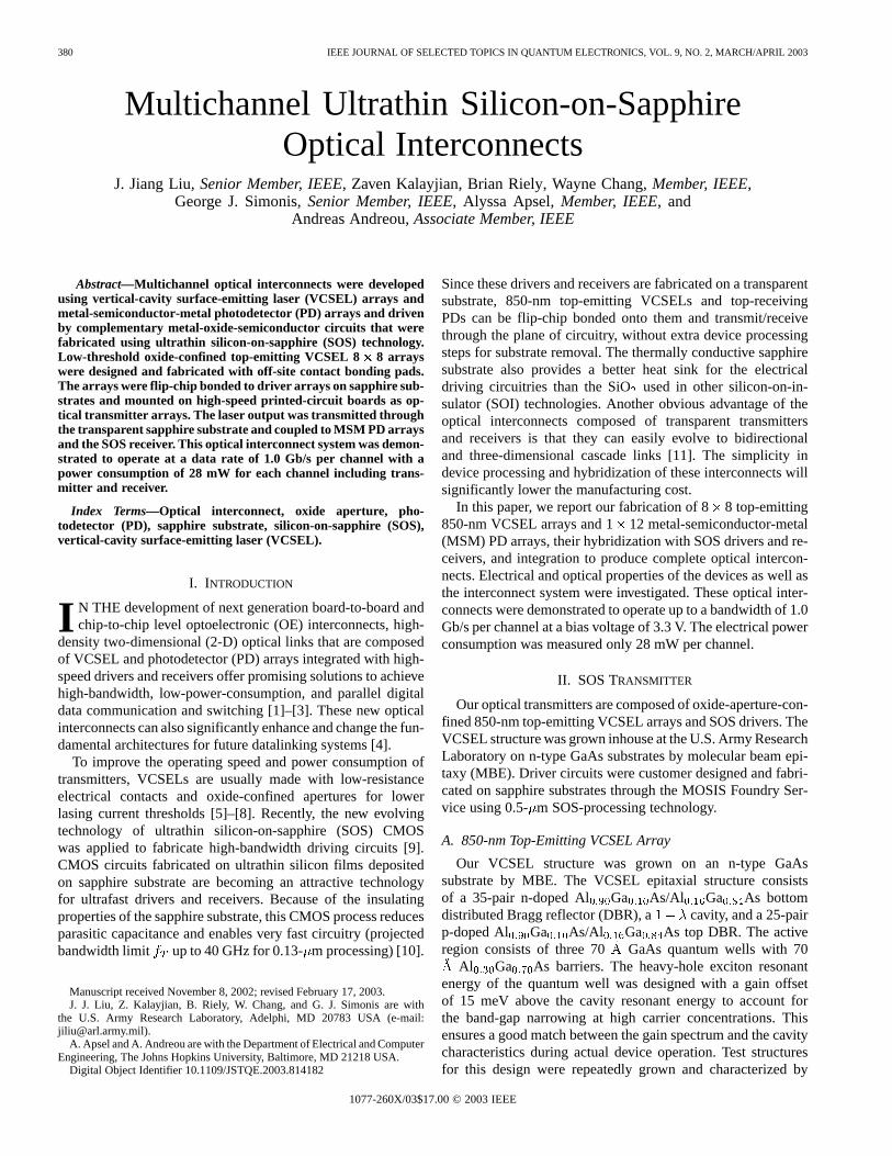
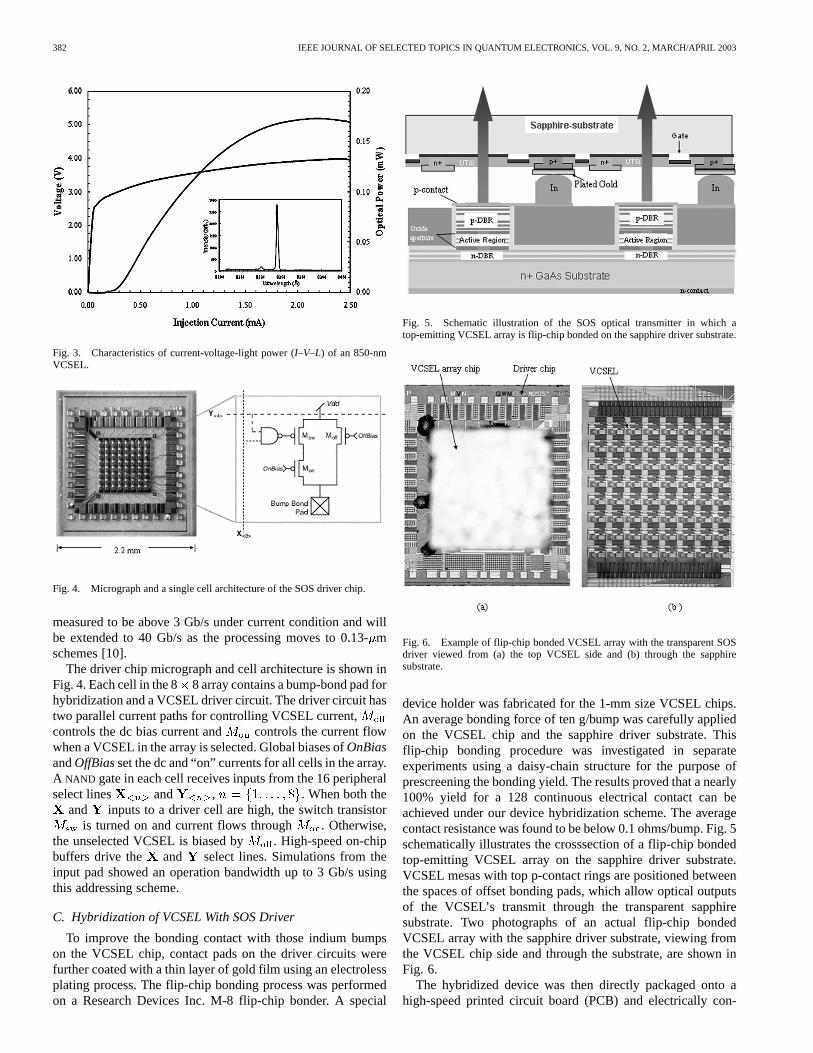
The device processing starts with an N-contact metal depo-sition on the top DBR contact layer. A BCl Cl reactiveion etching (RIE) process produced 32-m-diameter, 4-m-tall,and 125- m-pitch 8 8 VCSEL mesa arrays with the AlAs ox-idation layers exposed. Wet oxidation process was carried outto form the oxide confinement aperture. The resultant mesaswere passivated by low-temperature plasma-enhanced chemicalvapor deposition (PECVD) of 5000 SiO layer. Spin coatedcyclotene (BCB) resin was applied on the mesa structure forplanarization. As a special design for future flip-chip bonding ofthe device, we used an interconnecting metal deposition processto form offset electrical contacts to the p-contacts of the mesas.Patterned Indium bumps of 40m in diameter were depositedby e-beam evaporation on top of the offset electrical contactsfor flip-chip bonding. Fig. 1 shows a processed top-emittingVCSEL 8 8 array with a detailed callout of several devices.A cross sectional view of the structure of an individual VCSELis illustrated in Fig. 2. The N-contact for the VCSEL was placedon the backside of the GaAs substrate by depositing Ge/Ni/Aumetal film. After these fabrication procedures, the 88 VCSELarrays were diced out and prepared for hybridization with driverchips.
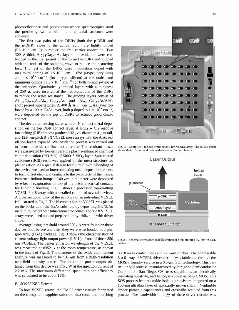
Average lasing threshold around 250A were found on thesedevices both before and after they were wire bonded in a pin-grid-array (PGA) package. Fig. 3 shows the characteristics ofcurrent-voltage-light output power (I-V-L) of one of those 850nm VCSELs. The center emission wavelength of the VCSELwas measured at 8352 at the room temperature, as shownin the insert of Fig. 3. The diameter of the oxide confinementaperture was measured to be 5.6m from a high-resolutionnear-field intensity pattern. The maximum power output ob-tained from this device was 175W at the injection current of2.2 mA. The maximum differential quantum slope efficiencywas calculated to be about 12%.
B. SOS VCSEL Drivers
To host VCSEL arrays, the CMOS driver circuits fabricatedon the transparent sapphire substrate also contained matching
Fig. 1. Complete 8� 8 top-emitting 850-nm VCSEL array. The callout detailshows their offsite bond pads with deposited Indium bumps.
Fig. 2. Schematic crosssectional illustration of a top-emitting 850-nm VCSELdevice.
8 8 array contact pads and 125-m pitches. The addressable8 8 array of VCSEL driver circuits was fabricated through theMOSIS foundry service in a 0.5-m SOI technology. This par-ticular SOI process, manufactured by Peregrine SemiconductorCorporation, San Diego, CA, uses sapphire as an electricallyinsulating substrate, and hence, is known as SOS CMOS. ThisSOS process features oxide-isolated transistors integrated on a100-nm ultrathin layer of epitaxially grown silicon. Negligibledevice parasitic capacitances and crosstalks resulted from thisprocess. The bandwidth limit of these driver circuits was
382 IEEE JOURNAL OF SELECTED TOPICS IN QUANTUM ELECTRONICS, VOL. 9, NO. 2, MARCH/APRIL 2003
Fig. 3. Characteristics of current-voltage-light power (I–V–L) of an 850-nmVCSEL.
Fig. 4. Micrograph and a single cell architecture of the SOS driver chip.
measured to be above 3 Gb/s under current condition and willbe extended to 40 Gb/s as the processing moves to 0.13-mschemes [10].
The driver chip micrograph and cell architecture is shown inFig. 4. Each cell in the 8 8 array contains a bump-bond pad forhybridization and a VCSEL driver circuit. The driver circuit hastwo parallel current paths for controlling VCSEL current,controls the dc bias current and controls the current flowwhen a VCSEL in the array is selected. Global biases ofOnBiasandOffBiasset the dc and “on” currents for all cells in the array.A NAND gate in each cell receives inputs from the 16 peripheralselect lines and , . When both the
and inputs to a driver cell are high, the switch transistoris turned on and current flows through . Otherwise,
the unselected VCSEL is biased by . High-speed on-chipbuffers drive the and select lines. Simulations from theinput pad showed an operation bandwidth up to 3 Gb/s usingthis addressing scheme.
C. Hybridization of VCSEL With SOS Driver
To improve the bonding contact with those indium bumpson the VCSEL chip, contact pads on the driver circuits werefurther coated with a thin layer of gold film using an electrolessplating process. The flip-chip bonding process was performedon a Research Devices Inc. M-8 flip-chip bonder. A special
Fig. 5. Schematic illustration of the SOS optical transmitter in which atop-emitting VCSEL array is flip-chip bonded on the sapphire driver substrate.
Fig. 6. Example of flip-chip bonded VCSEL array with the transparent SOSdriver viewed from (a) the top VCSEL side and (b) through the sapphiresubstrate.
device holder was fabricated for the 1-mm size VCSEL chips.An average bonding force of ten g/bump was carefully appliedon the VCSEL chip and the sapphire driver substrate. Thisflip-chip bonding procedure was investigated in separateexperiments using a daisy-chain structure for the purpose ofprescreening the bonding yield. The results proved that a nearly100% yield for a 128 continuous electrical contact can beachieved under our device hybridization scheme. The averagecontact resistance was found to be below 0.1 ohms/bump. Fig. 5schematically illustrates the crosssection of a flip-chip bondedtop-emitting VCSEL array on the sapphire driver substrate.VCSEL mesas with top p-contact rings are positioned betweenthe spaces of offset bonding pads, which allow optical outputsof the VCSEL’s transmit through the transparent sapphiresubstrate. Two photographs of an actual flip-chip bondedVCSEL array with the sapphire driver substrate, viewing fromthe VCSEL chip side and through the substrate, are shown inFig. 6.
The hybridized device was then directly packaged onto ahigh-speed printed circuit board (PCB) and electrically con-
LIU et al.: MULTICHANNEL ULTRATHIN SOS OPTICAL INTERCONNECTS 383
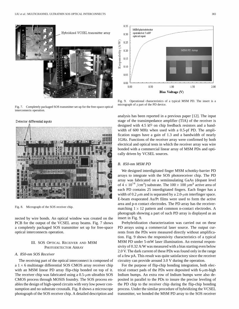
Fig. 7. Completely packaged SOS transmitter set up for the free-space opticalinterconnects operation.
Fig. 8. Micrograph of the SOS receiver chip.
nected by wire bonds. An optical window was created on thePCB for the output of the VCSEL array beams. Fig. 7 showsa completely packaged SOS transmitter set up for free-spaceoptical interconnects operation.
III. SOS OPTICAL RECEIVER AND MSMPHOTODETECTORARRAY
A. 850-nm SOS Receiver
The receiving part of the optical interconnect is composed ofa 1 6 multistage differential SOS CMOS array receiver chipwith an MSM linear PD array flip-chip bonded on top of it.The receiver chip was fabricated using a 0.5-m ultrathin SOSCMOS process through MOSIS foundry. The SOS process en-ables the design of high-speed circuits with very low power con-sumption and no substrate crosstalk. Fig. 8 shows a microscopephotograph of the SOS receiver chip. A detailed description and
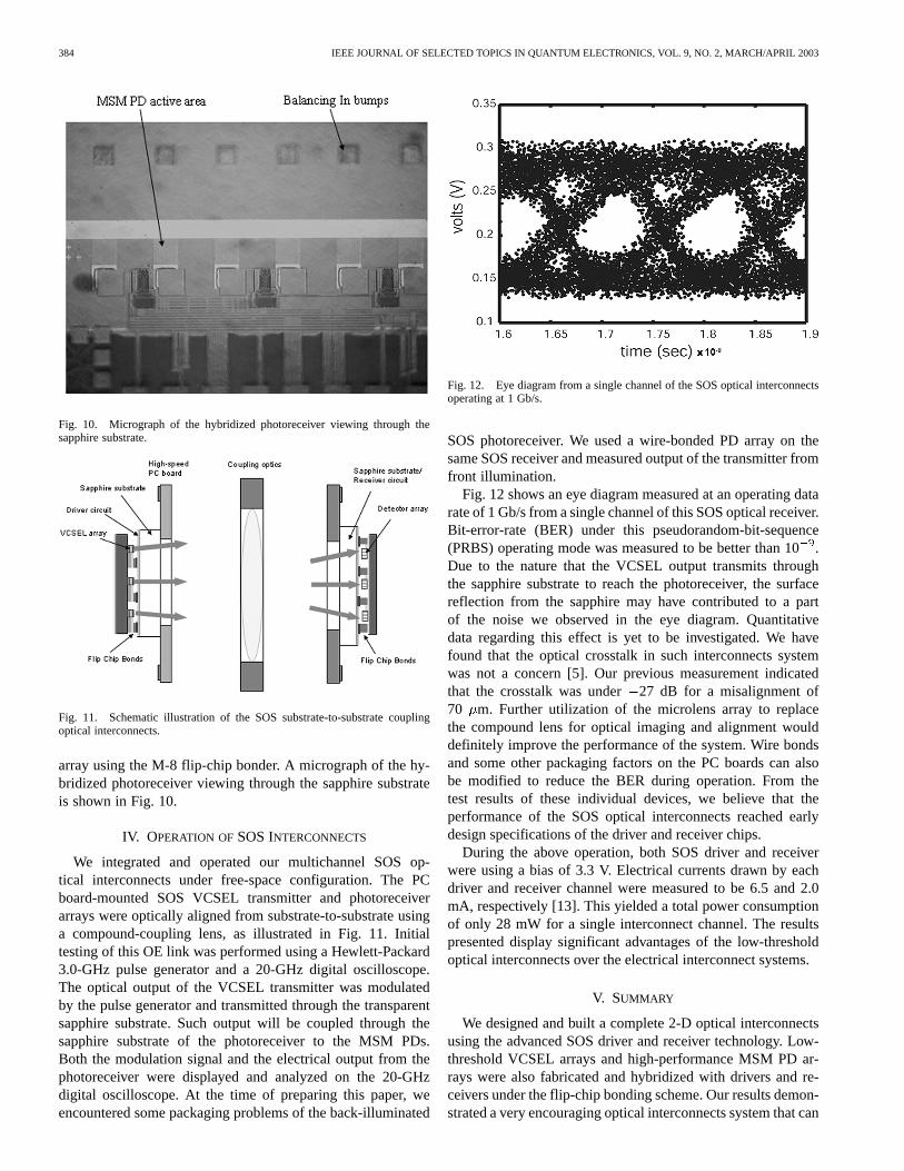
Fig. 9. Operational characteristics of a typical MSM PD. The insert is amicrograph of a part of the PD device.
analysis has been reported in a previous paper [12]. The inputstage of the transimpedance amplifier (TIA) of the receiver isdesigned with 4.5 k on chip feedback resistors and a band-width of 600 MHz when used with a 0.5-pf PD. The ampli-fication stages have a gain of 1.3 and a bandwidth of nearly1GHz. Functions of the receiver array were confirmed by bothelectrical and optical tests in which the receiver array was wirebonded with a commercial linear array of MSM PDs and opti-cally driven by VCSEL sources.
B. 850-nm MSM PD
We designed interdigitated finger MSM schottky-barrier PDarrays to integrate with the SOS photoreceiver chip. The PDarray was fabricated on a semiinsulating GaAs (dopant levelof 4 10 cm ) substrate. The 100 100 m active area ofeach PD contains 25 interdigitated fingers. Each finger has awidth of 0.2 m and is separated by a 2.0-m interfinger space.E-beam evaporated Au/Pt films were used to form the activearea and p-n contact electrodes. The PD array has the receiver-matching 1 12 pattern and common n-contact electrodes. Aphotograph showing a part of such PD array is displayed as aninsert in Fig. 9.
Prehybridization characterization was carried out on thesePD arrays using a commercial laser source. The output cur-rents from the PDs were measured directly without amplifica-tion. Fig. 9 shows the responsivity characteristics of a typicalMSM PD under 5-mW laser illumination. An external respon-sivity of 0.32 A/W was measured with a bias starting even below2.0 V. The dark current of these PDs was found only in the rangeof a few pA. This result was quite satisfactory since the receivercircuitry can provide around 3.0 V during the operation.
For the purpose of flip-chip bonding integration, both elec-trical contact pads of the PDs were deposited with 6-m-highIndium bumps. An extra row of Indium bumps were also de-posited in parallel to the PDs to insure the precise leveling ofthe PD chip to the receiver chip during the flip-chip bondingprocess. Under the similar procedure of hybridizing the VCSELtransmitter, we bonded the MSM PD array to the SOS receiver
384 IEEE JOURNAL OF SELECTED TOPICS IN QUANTUM ELECTRONICS, VOL. 9, NO. 2, MARCH/APRIL 2003
Fig. 10. Micrograph of the hybridized photoreceiver viewing through thesapphire substrate.
Fig. 11. Schematic illustration of the SOS substrate-to-substrate couplingoptical interconnects.
array using the M-8 flip-chip bonder. A micrograph of the hy-bridized photoreceiver viewing through the sapphire substrateis shown in Fig. 10.
IV. OPERATION OFSOS INTERCONNECTS
We integrated and operated our multichannel SOS op-tical interconnects under free-space configuration. The PCboard-mounted SOS VCSEL transmitter and photoreceiverarrays were optically aligned from substrate-to-substrate usinga compound-coupling lens, as illustrated in Fig. 11. Initialtesting of this OE link was performed using a Hewlett-Packard3.0-GHz pulse generator and a 20-GHz digital oscilloscope.The optical output of the VCSEL transmitter was modulatedby the pulse generator and transmitted through the transparentsapphire substrate. Such output will be coupled through thesapphire substrate of the photoreceiver to the MSM PDs.Both the modulation signal and the electrical output from thephotoreceiver were displayed and analyzed on the 20-GHzdigital oscilloscope. At the time of preparing this paper, weencountered some packaging problems of the back-illuminated
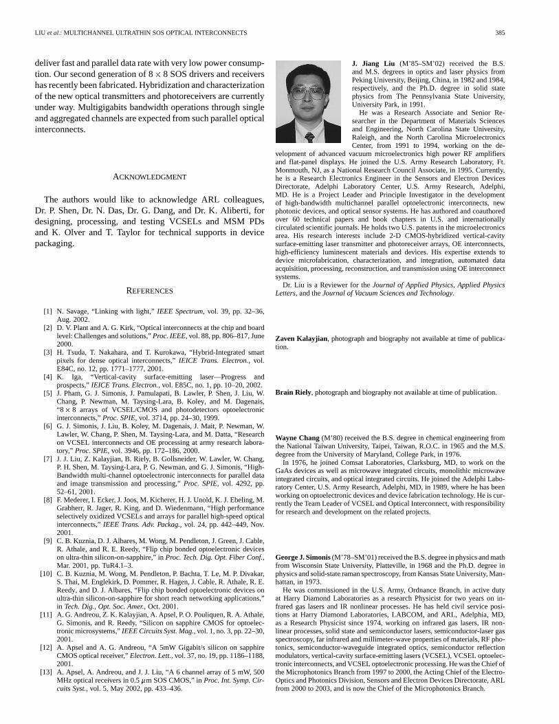
Fig. 12. Eye diagram from a single channel of the SOS optical interconnectsoperating at 1 Gb/s.
SOS photoreceiver. We used a wire-bonded PD array on thesame SOS receiver and measured output of the transmitter fromfront illumination.
Fig. 12 shows an eye diagram measured at an operating datarate of 1 Gb/s from a single channel of this SOS optical receiver.Bit-error-rate (BER) under this pseudorandom-bit-sequence(PRBS) operating mode was measured to be better than 10.Due to the nature that the VCSEL output transmits throughthe sapphire substrate to reach the photoreceiver, the surfacereflection from the sapphire may have contributed to a partof the noise we observed in the eye diagram. Quantitativedata regarding this effect is yet to be investigated. We havefound that the optical crosstalk in such interconnects systemwas not a concern [5]. Our previous measurement indicatedthat the crosstalk was under27 dB for a misalignment of70 m. Further utilization of the microlens array to replacethe compound lens for optical imaging and alignment woulddefinitely improve the performance of the system. Wire bondsand some other packaging factors on the PC boards can alsobe modified to reduce the BER during operation. From thetest results of these individual devices, we believe that theperformance of the SOS optical interconnects reached earlydesign specifications of the driver and receiver chips.
During the above operation, both SOS driver and receiverwere using a bias of 3.3 V. Electrical currents drawn by eachdriver and receiver channel were measured to be 6.5 and 2.0mA, respectively [13]. This yielded a total power consumptionof only 28 mW for a single interconnect channel. The resultspresented display significant advantages of the low-thresholdoptical interconnects over the electrical interconnect systems.
V. SUMMARY
We designed and built a complete 2-D optical interconnectsusing the advanced SOS driver and receiver technology. Low-threshold VCSEL arrays and high-performance MSM PD ar-rays were also fabricated and hybridized with drivers and re-ceivers under the flip-chip bonding scheme. Our results demon-strated a very encouraging optical interconnects system that can
LIU et al.: MULTICHANNEL ULTRATHIN SOS OPTICAL INTERCONNECTS 385
deliver fast and parallel data rate with very low power consump-tion. Our second generation of 88 SOS drivers and receivershas recently been fabricated. Hybridization and characterizationof the new optical transmitters and photoreceivers are currentlyunder way. Multigigabits bandwidth operations through singleand aggregated channels are expected from such parallel opticalinterconnects.
ACKNOWLEDGMENT
The authors would like to acknowledge ARL colleagues,Dr. P. Shen, Dr. N. Das, Dr. G. Dang, and Dr. K. Aliberti, fordesigning, processing, and testing VCSELs and MSM PDsand K. Olver and T. Taylor for technical supports in devicepackaging.
REFERENCES
[1] N. Savage, “Linking with light,”IEEE Spectrum, vol. 39, pp. 32–36,Aug. 2002.
[2] D. V. Plant and A. G. Kirk, “Optical interconnects at the chip and boardlevel: Challenges and solutions,”Proc. IEEE, vol. 88, pp. 806–817, June2000.
[3] H. Tsuda, T. Nakahara, and T. Kurokawa, “Hybrid-Integrated smartpixels for dense optical interconnects,”IEICE Trans. Electron., vol.E84C, no. 12, pp. 1771–1777, 2001.
[4] K. Iga, “Vertical-cavity surface-emitting laser—Progress andprospects,”IEICE Trans. Electron., vol. E85C, no. 1, pp. 10–20, 2002.
[5] J. Pham, G. J. Simonis, J. Pamulapati, B. Lawler, P. Shen, J. Liu, W.Chang, P. Newman, M. Taysing-Lara, B. Koley, and M. Dagenais,“8� 8 arrays of VCSEL/CMOS and photodetectors optoelectronicinterconnects,”Proc. SPIE, vol. 3714, pp. 24–30, 1999.
[6] G. J. Simonis, J. Liu, B. Koley, M. Dagenais, J. Mait, P. Newman, W.Lawler, W. Chang, P. Shen, M. Taysing-Lara, and M. Datta, “Researchon VCSEL interconnects and OE processing at army research labora-tory,” Proc. SPIE, vol. 3946, pp. 172–186, 2000.
[7] J. J. Liu, Z. Kalayjian, B. Riely, B. Gollsneider, W. Lawler, W. Chang,P. H. Shen, M. Taysing-Lara, P. G. Newman, and G. J. Simonis, “High-Bandwidth multi-channel optoelectronic interconnects for parallel dataand image transmission and processing,”Proc. SPIE, vol. 4292, pp.52–61, 2001.
[8] F. Mederer, I. Ecker, J. Joos, M. Kicherer, H. J. Unold, K. J. Ebeling, M.Grabherr, R. Jager, R. King, and D. Wiedenmann, “High performanceselectively oxidized VCSELs and arrays for parallel high-speed opticalinterconnects,”IEEE Trans. Adv. Packag., vol. 24, pp. 442–449, Nov.2001.
[9] C. B. Kuznia, D. J. Albares, M. Wong, M. Pendleton, J. Green, J. Cable,R. Athale, and R. E. Reedy, “Flip chip bonded optoelectronic deviceson ultra-thin silicon-on-sapphire,” inProc. Tech. Dig. Opt. Fiber Conf.,Mar. 2001, pp. TuR4.1–3.
[10] C. B. Kuznia, M. Wong, M. Pendleton, P. Bachta, T. Le, M. P. Divakar,S. Thai, M. Englekirk, D. Pommer, R. Hagen, J. Cable, R. Athale, R. E.Reedy, and D. J. Albares, “Flip chip bonded optoelectronic devices onultra-thin silicon-on-sapphire for short reach networking applications,”in Tech. Dig., Opt. Soc. Amer., Oct. 2001.
[11] A. G. Andreou, Z. K. Kalayjian, A. Apsel, P. O. Pouliquen, R. A. Athale,G. Simonis, and R. Reedy, “Silicon on sapphire CMOS for optoelec-tronic microsystems,”IEEE Circuits Syst. Mag., vol. 1, no. 3, pp. 22–30,2001.
[12] A. Apsel and A. G. Andreou, “A 5mW Gigabit/s silicon on sapphireCMOS optical receiver,”Electron. Lett., vol. 37, no. 19, pp. 1186–1188,2001.
[13] A. Apsel, A. Andreou, and J. J. Liu, “A 6 channel array of 5 mW, 500MHz optical receivers in 0.5�m SOS CMOS,” inProc. Int. Symp. Cir-cuits Syst., vol. 5, May 2002, pp. 433–436.
J. Jiang Liu (M’85–SM’02) received the B.S.and M.S. degrees in optics and laser physics fromPeking University, Beijing, China, in 1982 and 1984,respectively, and the Ph.D. degree in solid statephysics from The Pennsylvania State University,University Park, in 1991.
He was a Research Associate and Senior Re-searcher in the Department of Materials Sciencesand Engineering, North Carolina State University,Raleigh, and the North Carolina MicroelectronicsCenter, from 1991 to 1994, working on the de-
velopment of advanced vacuum microelectronics high power RF amplifiersand flat-panel displays. He joined the U.S. Army Research Laboratory, Ft.Monmouth, NJ, as a National Research Council Associate, in 1995. Currently,he is a Research Electronics Engineer in the Sensors and Electron DevicesDirectorate, Adelphi Laboratory Center, U.S. Army Research, Adelphi,MD. He is a Project Leader and Principle Investigator in the developmentof high-bandwidth multichannel parallel optoelectronic interconnects, newphotonic devices, and optical sensor systems. He has authored and coauthoredover 60 technical papers and book chapters in U.S. and internationallycirculated scientific journals. He holds two U.S. patents in the microelectronicsarea. His research interests include 2-D CMOS-hybridized vertical-cavitysurface-emitting laser transmitter and photoreceiver arrays, OE interconnects,high-efficiency luminescent materials and devices. His expertise extends todevice microfabrication, characterization, and integration, automated dataacquisition, processing, reconstruction, and transmission using OE interconnectsystems.
Dr. Liu is a Reviewer for theJournal of Applied Physics, Applied PhysicsLetters, and theJournal of Vacuum Sciences and Technology.
Zaven Kalayjian, photograph and biography not available at time of publica-tion.
Brain Riely , photograph and biography not available at time of publication.
Wayne Chang(M’80) received the B.S. degree in chemical engineering fromthe National Taiwan University, Taipei, Taiwan, R.O.C. in 1965 and the M.S.degree from the University of Maryland, College Park, in 1976.
In 1976, he joined Comsat Laboratories, Clarksburg, MD, to work on theGaAs devices as well as microwave integrated circuits, monolithic microwaveintegrated circuits, and optical integrated circuits. He joined the Adelphi Labo-ratory Center, U.S. Army Research, Adelphi, MD, in 1989, where he has beenworking on optoelectronic devices and device fabrication technology. He is cur-rently the Team Leader of VCSEL and Optical Interconnect, with responsibilityfor research and development on the related projects.
George J. Simonis(M’78–SM’01) received the B.S. degree in physics and mathfrom Wisconsin State University, Platteville, in 1968 and the Ph.D. degree inphysics and solid-state raman spectroscopy, from Kansas State University, Man-hattan, in 1973.
He was commissioned in the U.S. Army, Ordnance Branch, in active dutyat Harry Diamond Laboratories as a research Physicist for two years on in-frared gas lasers and IR nonlinear processes. He has held civil service posi-tions at Harry Diamond Laboratories, LABCOM, and ARL, Adelphia, MD,as a Research Physicist since 1974, working on infrared gas lasers, IR non-linear processes, solid state and semiconductor lasers, semiconductor-laser gasspectroscopy, far infrared and millimeter-wave properties of materials, RF pho-tonics, semiconductor-waveguide integrated optics, semiconductor reflectionmodulators, vertical-cavity surface-emitting lasers (VCSEL), VCSEL optoelec-tronic interconnects, and VCSEL optoelectronic processing. He was the Chief ofthe Microphotonics Branch from 1997 to 2000, the Acting Chief of the Electro-Optics and Photonics Division, Sensors and Electron Devices Directorate, ARLfrom 2000 to 2003, and is now the Chief of the Microphotonics Branch.

386 IEEE JOURNAL OF SELECTED TOPICS IN QUANTUM ELECTRONICS, VOL. 9, NO. 2, MARCH/APRIL 2003
Alyssa Apsel(M’86) received the B.S. degree with distinction from SwarthmoreCollege, Swarthmore, PA, in 1995, the M.S. degree from California Institute ofTechnology, Pasadena, in 1996, and the Ph.D. degree from The Johns HopkinsUniversity, Baltimore, MD, in 2002.
She is currently the Clare Luce Boothe Assistant Professor of Electricaland Computer Engineering, Cornell University, Ithaca, NY. Her dissertationresearch focused on the design, implementation, and analysis of optoelectronicsystems in silicon on sapphire very large scale integration (VLSI). Her currentresearch interests include analog, high-speed, and optoelectric VLSI.
Prof. Aspel received a Caltech Institute Fellowship in 1995, an Aspel WolmanFellowship in 1997, and a Clare Luce Boothe Professorship in 2002. She is alsothe recipient of the Best Student Paper Award for the 2000 Midwest Symposiumon Circuits and Systems.
Andreas Andreou(S’00–A’00), photograph and biography not available at timeof publication.
Related Documents