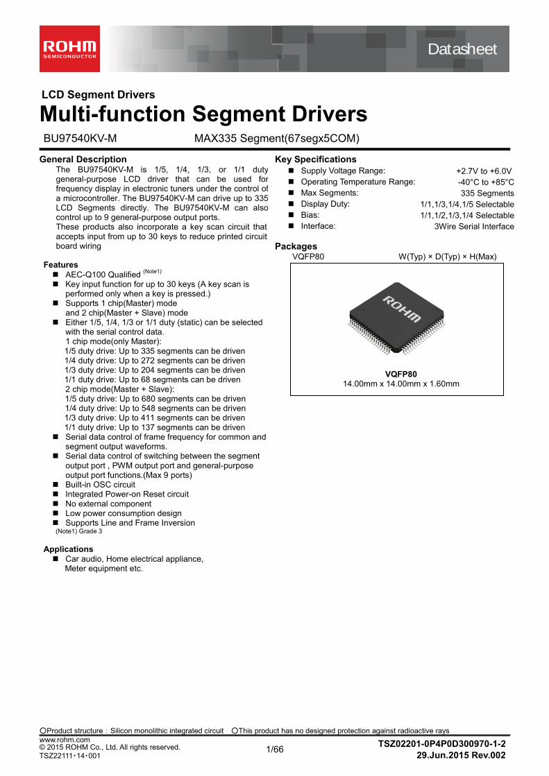
Datasheet ○Product structure:Silicon monolithic integrated circuit ○This product has no designed protection against radioactive rays . 1/66 TSZ02201-0P4P0D300970-1-2 © 2015 ROHM Co., Ltd. All rights reserved. 29.Jun.2015 Rev.002 TSZ22111・14・001 www.rohm.com LCD Segment Drivers Multi-function Segment Drivers BU97540KV-M MAX335 Segment(67segx5COM) General Description The BU97540KV-M is 1/5, 1/4, 1/3, or 1/1 duty general-purpose LCD driver that can be used for frequency display in electronic tuners under the control of a microcontroller. The BU97540KV-M can drive up to 335 LCD Segments directly. The BU97540KV-M can also control up to 9 general-purpose output ports. These products also incorporate a key scan circuit that accepts input from up to 30 keys to reduce printed circuit board wiring Features AEC-Q100 Qualified (Note1) Key input function for up to 30 keys (A key scan is performed only when a key is pressed.) Supports 1 chip(Master) mode and 2 chip(Master + Slave) mode Either 1/5, 1/4, 1/3 or 1/1 duty (static) can be selected with the serial control data. 1 chip mode(only Master): 1/5 duty drive: Up to 335 segments can be driven 1/4 duty drive: Up to 272 segments can be driven 1/3 duty drive: Up to 204 segments can be driven 1/1 duty drive: Up to 68 segments can be driven 2 chip mode(Master + Slave): 1/5 duty drive: Up to 680 segments can be driven 1/4 duty drive: Up to 548 segments can be driven 1/3 duty drive: Up to 411 segments can be driven 1/1 duty drive: Up to 137 segments can be driven Serial data control of frame frequency for common and segment output waveforms. Serial data control of switching between the segment output port , PWM output port and general-purpose output port functions.(Max 9 ports) Built-in OSC circuit Integrated Power-on Reset circuit No external component Low power consumption design Supports Line and Frame Inversion (Note1) Grade 3 Applications Car audio, Home electrical appliance, Meter equipment etc. Key Specifications Supply Voltage Range: Operating Temperature Range: Max Segments: Display Duty: Bias: Interface: + +2.7V to +6.0V -40°C to +85°C 335 Segments 1/1,1/3,1/4,1/5 Selectable 1/1,1/2,1/3,1/4 Selectable 3Wire Serial Interface Packages VQFP80 W(Typ) × D(Typ) × H(Max) VQFP80 14.00mm x 14.00mm x 1.60mm

Welcome message from author
This document is posted to help you gain knowledge. Please leave a comment to let me know what you think about it! Share it to your friends and learn new things together.
Transcript
Datasheet
Product structure:Silicon monolithic integrated circuit This product has no designed protection against radioactive rays
.
1/66
TSZ02201-0P4P0D300970-1-2
© 2015 ROHM Co., Ltd. All rights reserved. 29.Jun.2015 Rev.002 TSZ22111・14・001
www.rohm.com
LCD Segment Drivers
Multi-function Segment Drivers BU97540KV-M MAX335 Segment(67segx5COM)
General Description The BU97540KV-M is 1/5, 1/4, 1/3, or 1/1 duty general-purpose LCD driver that can be used for frequency display in electronic tuners under the control of a microcontroller. The BU97540KV-M can drive up to 335 LCD Segments directly. The BU97540KV-M can also control up to 9 general-purpose output ports. These products also incorporate a key scan circuit that accepts input from up to 30 keys to reduce printed circuit board wiring
Features
AEC-Q100 Qualified (Note1)
Key input function for up to 30 keys (A key scan is
performed only when a key is pressed.) Supports 1 chip(Master) mode
and 2 chip(Master + Slave) mode Either 1/5, 1/4, 1/3 or 1/1 duty (static) can be selected
with the serial control data. 1 chip mode(only Master):
1/5 duty drive: Up to 335 segments can be driven 1/4 duty drive: Up to 272 segments can be driven 1/3 duty drive: Up to 204 segments can be driven 1/1 duty drive: Up to 68 segments can be driven
2 chip mode(Master + Slave): 1/5 duty drive: Up to 680 segments can be driven 1/4 duty drive: Up to 548 segments can be driven
1/3 duty drive: Up to 411 segments can be driven 1/1 duty drive: Up to 137 segments can be driven Serial data control of frame frequency for common and
segment output waveforms. Serial data control of switching between the segment
output port , PWM output port and general-purpose output port functions.(Max 9 ports)
Built-in OSC circuit Integrated Power-on Reset circuit No external component Low power consumption design Supports Line and Frame Inversion (Note1) Grade 3
Applications
Car audio, Home electrical appliance, Meter equipment etc.
Key Specifications
Supply Voltage Range:
Operating Temperature Range:
Max Segments:
Display Duty:
Bias:
Interface:
+ +2.7V to +6.0V
-40°C to +85°C
335 Segments
1/1,1/3,1/4,1/5 Selectable
1/1,1/2,1/3,1/4 Selectable
3Wire Serial Interface
Packages VQFP80 W(Typ) × D(Typ) × H(Max)
VQFP80 14.00mm x 14.00mm x 1.60mm
2/66
BU97540KV-M
TSZ02201-0P4P0D300970-1-2 © 2015 ROHM Co., Ltd. All rights reserved. 29.Jun.2015 Rev.002
www.rohm.com
TSZ22111・15・001
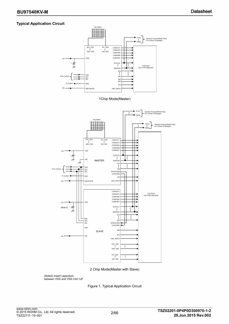
Typical Application Circuit
KS1 / S53
KS6 / S58
KI1 / S59
KI5 / S63
VDD
SCE
SCL
SDI
SDO
COM1/S71
COM2/S70
COM3/S69
COM4/S68
COM5/S67
S1/P1/G1
S9/P9/G9
S66/TESTIN
S10
S52
S64
S65
S72
OSC_IN/S73
LCD Panel
(Up to 335 Segments)
Key Matrix
P1/G1
P9/G9
From Control
To Control
+5V
(General Purpose/PWM Ports)
(For control of backlight)
*1
+5V
1Chip Mode(Master)
(General Purpose/PWM Ports)
(For control of backlight)
From Control
KS1 / S53
KS6 / S58
KI1 / S59
KI5 / S63
VDD
SCE
SCL
SDI
SDO
COM1/S71
COM2/S70
COM3/S69
COM4/S68
COM5/S67
S1/P1/G1
S9/P9/G9
S66
S10
S52
SYNCIO/S64
CLKIO/S65
S72
OSC_IN/S73
LCD Panel
(Up to 680 Segments)
P1/G1
P9/G9
+5V
*1
KS1 / S53
KS6 / S58
KI1 / S59
KI5 / S63
VDD
SCE
SCL
SDI
SDO
COM1/S71
COM2/S70
COM3/S69
COM4/S68
COM5/S67
S1/P1/G1
S9/P9/G9
S66/TESTIN
S10
S52
SYNCIO/S64
CLKIO/S65
S72
OSC_IN/S73
Key Matrix
P1/G1
P9/G9
To Control
+5V
*1
(General Purpose/PWM Ports)
(For control of backlight)
MASTER
SLAVE
MS
MS+5V
+5V
2 Chip Mode(Master with Slave)
Figure 1. Typical Application Circuit
(Note 2)
(Note2) Insert capacitors between VDD and VSS C≥0.1uF
3/66
BU97540KV-M
TSZ02201-0P4P0D300970-1-2 © 2015 ROHM Co., Ltd. All rights reserved. 29.Jun.2015 Rev.002
www.rohm.com
TSZ22111・15・001
KI4
/ S
62
KI3
/ S
61
KI2
/ S
60
KI1
/ S
59
KS
6 / S
58
KS
5 / S
57
KS
4 / S
56
KS
3 / S
55
KS
2 / S
54
KS
1 / S
53
S52
S51
S50
S49
S48
S47
S46
S45
S44
S43
KI5 / S63 S42
SYNCIO / S64 S41
CLKIO / S65 S40
S66 / TESTIN S39
COM5 / S67 S38
COM4 / S68 S37
COM3 / S69 S36
COM2 / S70 S35
COM1 / S71 S34
VDD S33
VSS S32
MS S31
SDO S30
S72 S29
OSC_IN / S73 S28
SCE S27
SCL S26
SDI S25
S1 / P1 / G1 S24
S2 / P2 / G2 S23
41
60
61
80 21
40
S3 / P
3 / G
3
S4 / P
4 / G
4
S5 / P
5 / G
5
S6 / P
6 / G
6
S7 / P
7 / G
7
S8 / P
8 / G
8
S9 / P
9 / G
9
S10
S11
S12
S13
S14
S15
S16
S17
S18
S19
S20
S21
S22
S1
/P1
/G1
S9
/P9
/G9
KI5
/ S
63
OSC / S73
POR
VSS
VDD
Shift Register
SEGMENT Driver/Latch
PWM RegisterControl Register
S1
0
S6
5/C
LK
IO
COMMON Driver
Clock /Timing
Generator
CO
M2
CO
M1
CO
M4
CO
M3
・・・
S6
4/S
YN
CIO
SCL
SDI
Serial Interface
SCE
SDO KEY BUFFER
KEY SCAN
KI4
/ S
62
KI3
/ S
61
KI2
/ S
60
KI1
/ S
59
KS
6/
S5
8
KS
5/
S5
7
KS
4/
S5
6
KS
3/
S5
5
KS
2/
S5
4
KS
1/
S5
3
・・・
MS
S6
7/C
OM
5
LCD voltage Generator
VLCD
VLCD2
VLCD1
VSS
S6
6/T
ES
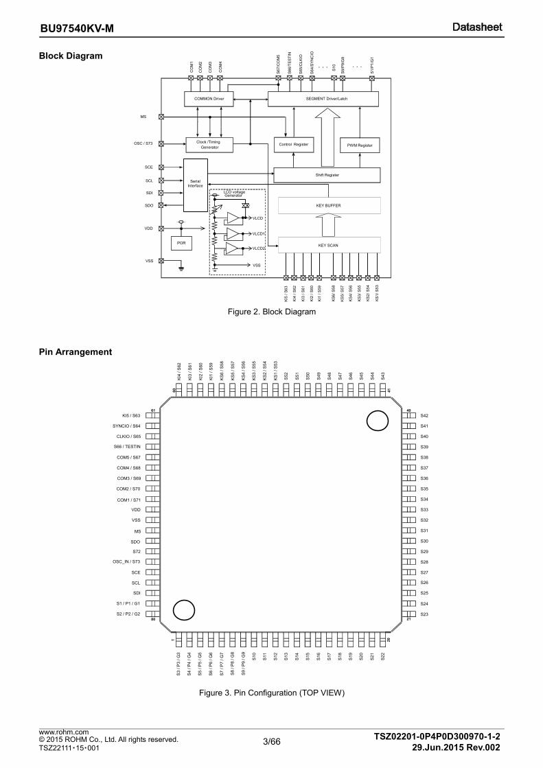
TINBlock Diagram
Figure 2. Block Diagram
Pin Arrangement
Figure 3. Pin Configuration (TOP VIEW)
4/66
BU97540KV-M
TSZ02201-0P4P0D300970-1-2 © 2015 ROHM Co., Ltd. All rights reserved. 29.Jun.2015 Rev.002
www.rohm.com
TSZ22111・15・001
Absolute Maximum Ratings (Ta = 25°C, VSS = 0V) Parameter Symbol Conditions Rating Unit
Maximum Supply Voltage VDD max VDD -0.3 to +7.0 V
Input Voltage VIN1 SCE, SCL, SDI -0.3 to +7.0 V
VIN2 KI1 to KI5 -0.3 to +7.0 V
Allowable Loss Pd 1.2 (Note3)
W
Operating Temperature Topr -40 to +85 °C
Storage Temperature Tstg -55 to +125 °C (Note3) When use more than Ta=25°C, subtract 12mW per degree. (Using ROHM standard board)
(Board size: 70mm×70mm×1.6mm material: FR4 board copper foil: land pattern only)
Caution: Operating the IC over the absolute maximum ratings may damage the IC. The damage can either be a short circuit between pins or an open circuit
between pins and the internal circuitry. Therefore, it is important to consider circuit protection measures, such as adding a fuse, in case the IC is operated over the
absolute maximum ratings.
Recommend Operating Conditions (Ta = -40°C to +85°C, VSS = 0V)
Parameter Symbol Conditions Rating
Unit Min Typ Max
Supply Voltage VDD 2.7 5.0 6.0 V
Electrical Characteristics for the Allowable Operating Ranges
Parameter Symbol Pin Conditions Limit
Unit Min Typ Max
Hysteresis VH1 SCE, SCL, SDI - 0.03 VDD - V
VH2 KI1 to KI5 - 0.1 VDD - V
Power-on Detection Voltage
VDET VDD 1.3 1.8 2.2 V
“H” Level Input Voltage VIH1 SCE,SCL,SDI, SYNCIO,CLKIO
4.5V ≤ VDD ≤ 6.0V 0.4VDD - VDD V
VIH2 SCE, SCL, SDI, SYNCIO,CLKIO
2.7V ≤ VDD < 4.5V 0.8VDD - VDD
VIH3 KI1 to KI5 0.7VDD - VDD
“L” Level Input Voltage VIL1 SCE, SCL, SDI KI1 to KI5 SYNCIO,CLKIO
0 - 0.2VDD V
Input Floating Voltage VIF KI1 to KI5 - - 0.05VDD V
Pull-down Resistance RPD KI1 to KI5 VDD=5.0V 50 100 250 KΩ
Output Off Leakage Current
IOFFH SDO VO=6.0V - - 6.0 µA
“H” Level Input Current IIH1
SCE, SCL, SDI SYNCIO,CLKIO
VI = 5.5V - - 5.0 µA
“L” Level Input Current IIL1
SCE, SCL, SDI SYNCIO,CLKIO
VI = 0V -5.0 - - µA
“H” Level Output Voltage
VOH1 S1 to S73 IO = -20µA, VLCD=1.00*VDD
VDD-0.9 - -
V
VOH2 COM1 to COM5 IO = -100µA, VDD=1.00*VDD
VDD-0.9 - -
VOH3 P1/G1 to P9/G9 IO = -1mA VDD-0.9 - -
VOH4 KS1 to KS6 IO = -500uA VDD-1.0 VDD-0.5 VDD-0.2
VOH5 SYNCIO,CLKIO IO = -1mA VDD-0.9 - -
“L” Level Output Voltage
VOL1 S1 to S70 IO = 20µA - - 0.9
V
VOL2 COM1 to COM5 IO = 100µA - - 0.9
VOL3 P1/G1 to P9/G9 IO = 1mA - - 0.9
VOL4 KS1 to KS6 IO = 25uA 0.2 0.5 1.5
VOL5 SDO IO = 1mA - 0.1 0.5
VOL6 SYNCIO,CLKIO IO = 1mA - - 0.9
Middle Level Output Voltage
VMID1 S1 to S73 1/2 bias IO = ±20µA VLCD=1.00*VDD
1/2 VDD -0.9
- 1/2 VDD
+0.9
V
VMID2 COM1 to COM5 1/2 bias IO = ±100µA VLCD=1.00*VDD
1/2 VDD -0.9
- 1/2 VDD
+0.9
VMID3 S1 to S73 1/3 bias IO = ±20µA VLCD=1.00*VDD
2/3 VDD -0.9
- 2/3 VDD
+0.9
VMID4 S1 to S73 1/3 bias IO = ±20µA VLCD=1.00*VDD
1/3 VDD -0.9
- 1/3 VDD
+0.9
VMID5 COM1 to COM5 1/3 bias IO = ±100µA VLCD=1.00*VDD
2/3 VDD -0.9
- 2/3 VDD
+0.9
VMID6 COM1 to COM5 1/3 bias IO = ±100µA VLCD=1.00*VDD
1/3 VDD -0.9
- 1/3 VDD
+0.9
5/66
BU97540KV-M
TSZ02201-0P4P0D300970-1-2 © 2015 ROHM Co., Ltd. All rights reserved. 29.Jun.2015 Rev.002
www.rohm.com
TSZ22111・15・001
Electrical Characteristics – continued
Parameter Symbol Pin Conditions Limit
Unit Min Typ Max
Current Consumption IDD1 VDD Power-saving mode - - 15 µA
IDD2 VDD 1chip mode VDD = 5.0V Output open, 1/2 bias Frame frequency=80Hz VLCD=1.00*VDD
- 105 220 µA
IDD3 VDD 1chip mode VDD = 5.0V Output open,1/3 bias Frame frequency=80Hz VLCD=1.00*VDD
- 130 270 µA
IDD4 VDD 2chip mode : Master VDD = 5.0V Output open,1/3 bias Frame frequency=80Hz VLCD=1.00*VDD
- 195 370 µA
IDD5 VDD 2chip mode : Slave VDD = 5.0V Output open,1/3 bias Frame frequency=80Hz VLCD=1.00*VDD
- 105 220 µA
Oscillation Characteristics (Ta = -40 to +85°C, VDD = 2.7V to 6.0V, VSS = 0.0V)
Parameter Symbol Pin Conditions Limit
Unit Min Typ Max
Oscillator Frequency 1 fosc1 - VDD = 2.7V to 6.0V 300 - 720 kHz
Oscillator Frequency 2 fosc2 - VDD = 5.0V 540 600 660 kHz
Oscillator Frequency 3 fosc3 - VDD = 6.0V 562 625 688 kHz
External Clock Frequency
(Note4)
fosc4 OSC_IN/S73 External clock mode (OC=1)
30 - 1000 kHz
External Clock Duty tdty OSC_IN/S73 External clock mode (OC=1)
30 50 70 %
(Note4) Frame frequency is decided external frequency and dividing ratio of FC0 to FC3 setting.
【Reference Data】
Figure 4. Typical Temperature Characteristics
300
350
400
450
500
550
600
650
700
-40 -20 0 20 40 60 80
Temperature[°C]
fosc[k
Hz]
VDD = 6.0V
VDD = 5.0V
VDD = 3.3V
VDD = 2.7V
6/66
BU97540KV-M
TSZ02201-0P4P0D300970-1-2 © 2015 ROHM Co., Ltd. All rights reserved. 29.Jun.2015 Rev.002
www.rohm.com
TSZ22111・15・001
SDO CL
RPU Host
Power supply for I/O level
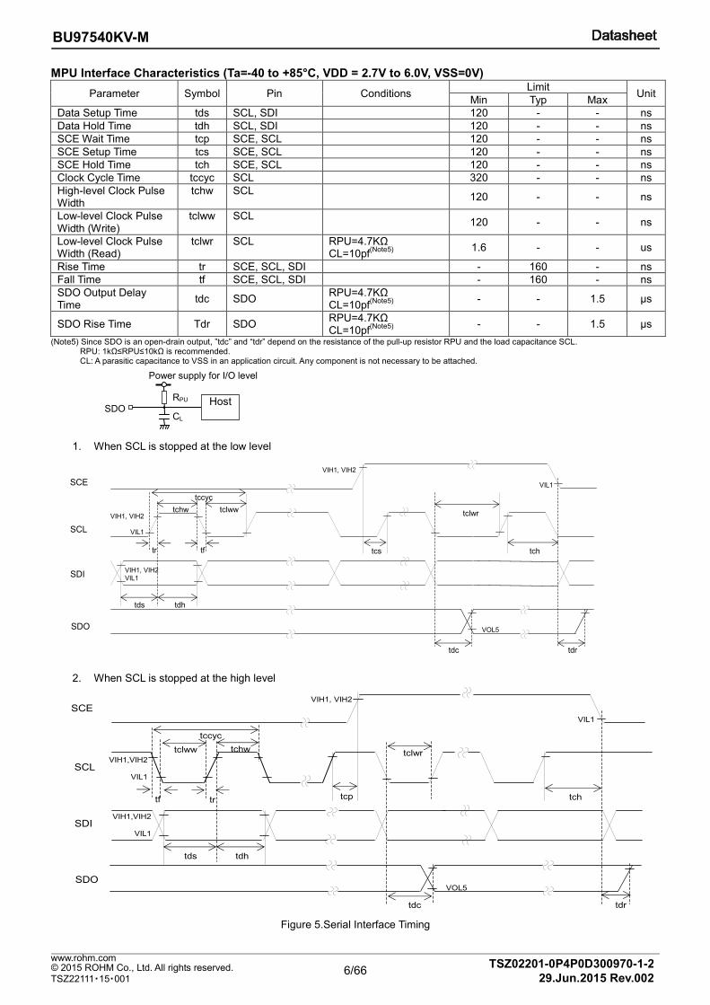
MPU Interface Characteristics (Ta=-40 to +85°C, VDD = 2.7V to 6.0V, VSS=0V)
Parameter Symbol Pin Conditions Limit
Unit Min Typ Max
Data Setup Time tds SCL, SDI 120 - - ns
Data Hold Time tdh SCL, SDI 120 - - ns
SCE Wait Time tcp SCE, SCL 120 - - ns
SCE Setup Time tcs SCE, SCL 120 - - ns
SCE Hold Time tch SCE, SCL 120 - - ns
Clock Cycle Time tccyc SCL 320 - - ns
High-level Clock Pulse Width
tchw SCL 120 - - ns
Low-level Clock Pulse Width (Write)
tclww SCL 120 - - ns
Low-level Clock Pulse Width (Read)
tclwr SCL RPU=4.7KΩ CL=10pf
(Note5)
1.6 - - us
Rise Time tr SCE, SCL, SDI - 160 - ns
Fall Time tf SCE, SCL, SDI - 160 - ns
SDO Output Delay Time
tdc SDO RPU=4.7KΩ CL=10pf
(Note5)
- - 1.5 µs
SDO Rise Time Tdr SDO RPU=4.7KΩ CL=10pf
(Note5)
- - 1.5 µs
(Note5) Since SDO is an open-drain output, ”tdc” and “tdr” depend on the resistance of the pull-up resistor RPU and the load capacitance SCL. RPU: 1kΩ≤RPU≤10kΩ is recommended. CL: A parasitic capacitance to VSS in an application circuit. Any component is not necessary to be attached.
1. When SCL is stopped at the low level
SDI
SCE
SCL
VIH1, VIH2VIL1
tds tdh
tchw tclww
tr tf tcs tch
VIH1, VIH2
VIL1
VIH1, VIH2
VIL1
tccyc
SDO
tdc tdr
VOL5
tclwr
2. When SCL is stopped at the high level
SDI
SCE
SCLVIH1,VIH2
VIL1
tds tdh
tclww tchw
tf tr tcp tch
VIH1, VIH2
VIL1
VIH1,VIH2
VIL1
tccyc
SDO
tdc tdr
VOL5
tclwr
Figure 5.Serial Interface Timing
7/66
BU97540KV-M
TSZ02201-0P4P0D300970-1-2 © 2015 ROHM Co., Ltd. All rights reserved. 29.Jun.2015 Rev.002
www.rohm.com
TSZ22111・15・001
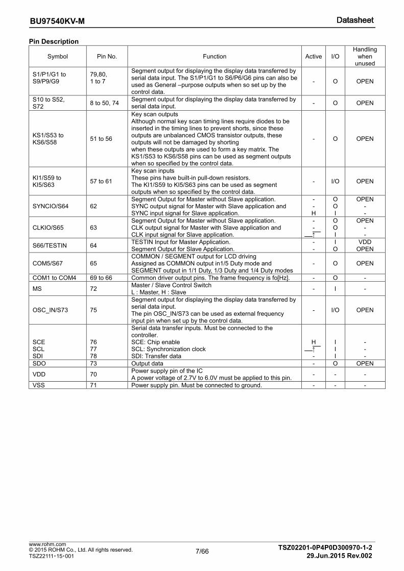
Pin Description
Symbol Pin No. Function Active I/O Handling
when unused
S1/P1/G1 to S9/P9/G9
79,80, 1 to 7
Segment output for displaying the display data transferred by serial data input. The S1/P1/G1 to S6/P6/G6 pins can also be used as General –purpose outputs when so set up by the control data.
- O OPEN
S10 to S52, S72
8 to 50, 74 Segment output for displaying the display data transferred by serial data input.
- O OPEN
KS1/S53 to KS6/S58
51 to 56
Key scan outputs Although normal key scan timing lines require diodes to be inserted in the timing lines to prevent shorts, since these outputs are unbalanced CMOS transistor outputs, these outputs will not be damaged by shorting when these outputs are used to form a key matrix. The KS1/S53 to KS6/S58 pins can be used as segment outputs when so specified by the control data.
- O OPEN
KI1/S59 to KI5/S63
57 to 61
Key scan inputs These pins have built-in pull-down resistors. The KI1/S59 to KI5/S63 pins can be used as segment outputs when so specified by the control data.
- I/O OPEN
SYNCIO/S64 62 Segment Output for Master without Slave application. SYNC output signal for Master with Slave application and SYNC input signal for Slave application.
- - H
O O I
OPEN - -
CLKIO/S65 63 Segment Output for Master without Slave application. CLK output signal for Master with Slave application and CLK input signal for Slave application.
- - ↑
O O I
OPEN - -
S66/TESTIN 64 TESTIN Input for Master Application. Segment Output for Slave Application.
- -
I O
VDD OPEN
COM5/S67 65 COMMON / SEGMENT output for LCD driving Assigned as COMMON output in1/5 Duty mode and SEGMENT output in 1/1 Duty, 1/3 Duty and 1/4 Duty modes
- O OPEN
COM1 to COM4 69 to 66 Common driver output pins. The frame frequency is fo[Hz]. - O -
MS 72 Master / Slave Control Switch L : Master, H : Slave
- I -
OSC_IN/S73 75
Segment output for displaying the display data transferred by serial data input. The pin OSC_IN/S73 can be used as external frequency input pin when set up by the control data.
- I/O OPEN
SCE SCL SDI
76 77 78
Serial data transfer inputs. Must be connected to the controller. SCE: Chip enable SCL: Synchronization clock SDI: Transfer data
H ↑ -
I I I
- - -
SDO 73 Output data - O OPEN
VDD 70 Power supply pin of the IC A power voltage of 2.7V to 6.0V must be applied to this pin.
- - -
VSS 71 Power supply pin. Must be connected to ground. - - -
8/66
BU97540KV-M
TSZ02201-0P4P0D300970-1-2 © 2015 ROHM Co., Ltd. All rights reserved. 29.Jun.2015 Rev.002
www.rohm.com
TSZ22111・15・001
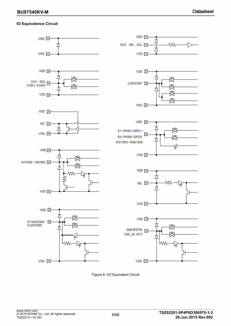
IO Equivalence Circuit
Figure 6. I/O Equivalent Circuit
9/66
BU97540KV-M
TSZ02201-0P4P0D300970-1-2 © 2015 ROHM Co., Ltd. All rights reserved. 29.Jun.2015 Rev.002
www.rohm.com
TSZ22111・15・001
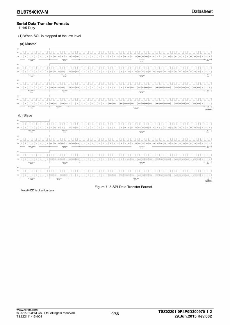
Serial Data Transfer Formats 1. 1/5 Duty
(1) When SCL is stopped at the low level (a) Master
D94 D95 D96 0 0 0 0
SCL
D2 D3 D4 ---D11 00 0 0 0 0 0 --- 0 DT0 DT1 KM0 KM1 KM2 FC3 OC SC BU0P0 P1 P2 P3 FL FC0 BU1 BU2 0 000 SSDR FC1 FC2
1 1 1 0 0 0
111
1 1 1 D190 D1910 0 0 1 0 D97 D192 0 0 0 0
SCE
D98 D99 D100 --- SSC0 0 0 0 0 --- PG8 PG9 PF00 0 PG1 PG2 PG3 PG40 CT3 0 1
0
0PF1 PF2 PF3 PF4 CT0
0 D193 D194 D195 D196
CT2CT1PG5 PG6 PG7
--- D286 D287 D288 0
SDI
SCE
SCL
SDI 1 0 0 0 0 0 0 0 0 --- 0 0 WN10 WN11 --- WN17 WN18 WN20 WN21 --- WN27 WN28 WN30 WN31 --- WN37 WN38 WN40 WN41 --- WN47 WN48 0 1 0
1 1 1 0 0 0 1 0 D289 D230 --- D334 D335 0 --- 0 0
SCE
SCL
SDI
SCE
SCL
0 0 0 0 0 0 0 WN50 --- WN57 WN58 WN60 ---WN61 --- WN67 WN68 WN70 WN71 WN88 WN90 WN91 --- WN97--- WN77 WN78 WN80 WN81SDI WN98 0 1 1
0
0
0
WN51 WN87
DD2 bits
Control Data54 bits
Display Data96 bits
Device Address8 bits
Device Address8 bits
Display Data96 bits
DD2 bits
Device Address8 bits
Display Data96 bits
DD2 bits
Device Address8 bits
Display Data47 bits
DD2 bits
Control Data54 bits
Control Data54 bits
Control Data103 bits
(b) Slave
SCE
SCL
SDI 0 0 0 1 0 0 1 0 D1 D2 D3 D4 --- D94 D95 D96 0 0 0 0 0 0 0 0 0 0 --- 0 DR SS DT0 DT1 KM0 KM1 KM2 P0 P1 P2 P3 FL FC0 FC1 FC2 FC3 OC SC BU0 BU1 BU2 0 0 0
SCE
SCL
SDI 0 0 0 1 0 0 1 0 D97 D98 D99 D100 --- D190 D191 D192 0 0 0 0 0 0 0 0 0 0 --- 0 0 SSC 0 PG1 PG2 PG3 PG4 PG5 CT1 CT2PG6 PG7 PG8 PG9 PF0 PF1 CT3 0 0 1
SCE
SCL
PF2 PF3 PF4 CT0
SDI 0 0 0 1 0 0 1 0 D193 D194 D195 D196 --- D286 D287 D288 0 0 0 0 0 0 0 0 0 0 --- 0 0 WN10 WN11 --- WN17 WN18 WN20 WN41 ---WN21 --- WN27 WN28 WN30 WN31 WN47 WN48 0 1 0
SCE
--- WN37 WN38 WN40
SCL
SDI 0 0 0 1 0 0 1 0 D289 D230 --- D354 D355 0 --- 0 0 0 0 0 0 0 0 0 WN50 WN51 --- WN57 WN58 WN60 WN61 --- WN67 WN68 WN70 WN71 --- WN77 WN78 WN80 WN81 --- WN87 WN88 WN90 WN91 --- WN97 WN98 0 1 1
DD2 bits
Display Data96 bits
Device Address8 bits
Device Address8 bits
Display Data96 bits
DD2 bits
Device Address8 bits
Display Data96 bits
DD2 bits
Device Address8 bits
DD2 bits
Control Data54 bits
Control Data54 bits
Control Data54 bits
Display Data67 bits
Control Data83 bits
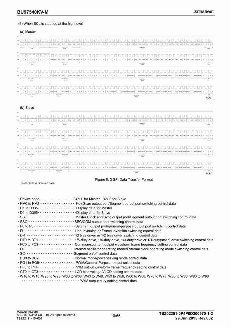
Figure 7. 3-SPI Data Transfer Format
(Note6) DD is direction data.
(Note6)
(Note6)
10/66
BU97540KV-M
TSZ02201-0P4P0D300970-1-2 © 2015 ROHM Co., Ltd. All rights reserved. 29.Jun.2015 Rev.002
www.rohm.com
TSZ22111・15・001
(2) When SCL is stopped at the high level
(a) Master
SCE
SCL
SDI 1 1 1 0 0 0 1 0 D1 D2 D3 D4 --- D94 D95 D96 0 0 0 0 0 0 0 0 0 0 --- 0 DR SS DT0 DT1 KM0 KM1 KM2 P0 P1 P2 P3 FL FC0 FC1 FC2 FC3 OC SC BU0 BU1 BU2 0 0 0
SCE
SCL
SDI 1 1 1 0 0 0 1 0 D97 D98 D99 D100 --- D190 D191 D192 0 0 0 0 0 0 0 0 0 0 --- 0 0 SSC 0 PG1 PG2 PG3 PG4 PG5 CT1 CT2PG6 PG7 PG8 PG9 PF0 PF1 CT3 0 0 1
SCE
SCL
PF2 PF3 PF4 CT0
SDI 1 1 1 0 0 0 1 0 D193 D194 D195 D196 --- D286 D287 D288 0 0 0 0 0 0 0 0 0 0 --- 0 0 WN10 WN11 --- WN17 WN18 WN20 WN41 ---WN21 --- WN27 WN28 WN30 WN31 WN47 WN48 0 1 0
SCE
--- WN37 WN38 WN40
SCL
SDI 1 1 1 0 0 0 1 0 D289 D230 --- D334 D335 0 --- 0 0 0 0 0 0 0 0 0 WN50 WN51 --- WN57 WN58 WN60 WN61 --- WN67 WN68 WN70 WN71 --- WN77 WN78 WN80 WN81 --- WN87 WN88 WN90 WN91 --- WN97 WN98 0 1 1
DD2 bits
Display Data96 bits
Device Address8 bits
Device Address8 bits
Display Data96 bits
DD2 bits
Device Address8 bits
Display Data96 bits
DD2 bits
Device Address8 bits
DD2 bits
Control Data54 bits
Control Data54 bits
Control Data54 bits
Display Data47 bits
Control Data103 bits
(b) Slave
SCE
SCL
SDI 0 0 0 1 0 0 1 0 D1 D2 D3 D4 --- D94 D95 D96 0 0 0 0 0 0 0 0 0 0 --- 0 DR SS DT0 DT1 KM0 KM1 KM2 P0 P1 P2 P3 FL FC0 FC1 FC2 FC3 OC SC BU0 BU1 BU2 0 0 0
SCE
SCL
SDI 0 0 0 1 0 0 1 0 D97 D98 D99 D100 --- D190 D191 D192 0 0 0 0 0 0 0 0 0 0 --- 0 0 SSC 0 PG1 PG2 PG3 PG4 PG5 CT1 CT2PG6 PG7 PG8 PG9 PF0 PF1 CT3 0 0 1
SCE
SCL
PF2 PF3 PF4 CT0
SDI 0 0 0 1 0 0 1 0 D193 D194 D195 D196 --- D286 D287 D288 0 0 0 0 0 0 0 0 0 0 --- 0 0 WN10 WN11 --- WN17 WN18 WN20 WN41 ---WN21 --- WN27 WN28 WN30 WN31 WN47 WN48 0 1 0
SCE
--- WN37 WN38 WN40
SCL
SDI 0 0 0 1 0 0 1 0 D289 D230 --- D354 D355 0 --- 0 0 0 0 0 0 0 0 0 WN50 WN51 --- WN57 WN58 WN60 WN61 --- WN67 WN68 WN70 WN71 --- WN77 WN78 WN80 WN81 --- WN87 WN88 WN90 WN91 --- WN97 WN98 0 1 1
DD2 bits
Display Data96 bits
Device Address8 bits
Device Address8 bits
Display Data96 bits
DD2 bits
Device Address8 bits
Display Data96 bits
DD2 bits
Device Address8 bits
DD2 bits
Control Data54 bits
Control Data54 bits
Control Data54 bits
Display Data67 bits
Control Data83 bits
Figure 8. 3-SPI Data Transfer Format
(Note7) DD is direction data.
・Device code・・・・・・・・・・・・・・・・・・・・”47H” for Master , “48H” for Slave
・KM0 to KM2・・・・・・・・・・・・・・・・・・・・・Key Scan output port/Segment output port switching control data
・D1 to D335・・・・・・・・・・・・・・・・・・・・・・Display data for Master
・D1 to D355・・・・・・・・・・・・・・・・・・・・・・Display data for Slave
・SS・・・・・・・・・・・・・・・・・・・・・・・・・・・・・Master Clock and Sync output port/Segment output port switching control data
・SSC・・・・・・・・・・・・・・・・・・・・・・・・・・・SEG/COM output port switching control data
・P0 to P3・・・・・・・・・・・・・・・・・・・・・・・・Segment output port/general-purpose output port switching control data
・FL・・・・・・・・・・・・・・・・・・・・・・・・・・・・・Line Inversion or Frame Inversion switching control data
・DR・・・・・・・・・・・・・・・・・・・・・・・・・・・・1/3 bias driver or 1/2 bias driver switching control data
・DT0 to DT1・・・・・・・・・・・・・・・・・・・・・1/5-duty drive, 1/4-duty drive, 1/3-duty drive or 1/1-duty(static) drive switching control data
・FC0 to FC3・・・・・・・・・・・・・・・・・・・・・Common/segment output waveform frame frequency setting control data
・OC・・・・・・・・・・・・・・・・・・・・・・・・・・・ Internal oscillator operating mode/External clock operating mode switching control data
・SC・・・・・・・・・・・・・・・・・・・・・・・・・・・・Segment on/off control data
・BU0 to BU2・・・・・・・・・・・・・・・・・・・・・Normal mode/power-saving mode control data
・PG1 to PG9・・・・・・・・・・・・・・・・・・・・ PWM/General Purpose output select data
・PF0 to PF4・・・・・・・・・・・・・・・・・・・・・PWM output waveform frame frequency setting control data.
・CT0 to CT3・・・・・・・・・・・・・・・・・・・・・LCD bias voltage VLCD setting control data.
・W10 to W18, W20 to W28, W30 to W38, W40 to W48, W50 to W58, W60 to W68, W70 to W78, W80 to W88, W90 to W98
・・・・・・・・・・・・・・・・・・・・・・・・・・・・・・・・・・PWM output duty setting control data
(Note7)
(Note7)
11/66
BU97540KV-M
TSZ02201-0P4P0D300970-1-2 © 2015 ROHM Co., Ltd. All rights reserved. 29.Jun.2015 Rev.002
www.rohm.com
TSZ22111・15・001
2. 1/4 Duty (1) When SCL is stopped at the low level
(a) Master
D3 D41 1 1 0 0 0 --- D94 D95 D96 0
SCL
1 0 D1 D2 0 0 0 0 0 0 0 0 0 --- 0 DR SS DT0 DT1 KM0 KM1 KM2 P0 P1 P2 P3 FL FC0 FC1 FC2 FC3 OC SC BU0 BU1 BU2 0 0 0
1 1 1 0 0 D192 00 1 0 D97 D98 D99 0 0 0 0 0
SCE
D100 --- D190 D191 0 0 0 0 --- 0 PG8 PG90 SSC 0 PG1 PG2 PG3 1PF0 PF1 PF2 PF3 PF4 CT0
0
CT1 CT2 CT3 0 0PG4 PG5 PG6 PG7
0 D193 D194 --- D2711 1 1 0 0 D272 0 --- 0 0
SDI
SCE
SCL
SDI 1 0 0 0 0 0 0 0 0 0 --- 0 0 WN10 WN11 --- WN17 WN18 WN20 WN21 --- WN27 WN28 WN30 WN31 --- WN37 WN38 WN40 WN41 --- WN47 WN48 0 1 0
1 1 1 0 0 0 1 0 0 0 0 0 --- 0 0 0 0 0 0 0 0 0
SCE
SCL
SDI
SCE
SCL
0 0 WN50 WN51 --- WN57 WN78 WN80WN58 WN60 WN61 --- WN67 WN68 1WN81 --- WN87 WN88 WN90 WN91SDI --- WN97 WN98 0 1WN70 WN71 --- WN77
DD2 bits
Display Data96 bits
Device Address8 bits
Device Address8 bits
Display Data96 bits
DD2 bits
Device Address8 bits
DD2 bits
Device Address8 bits
DD2 bits
Control Data54 bits
Control Data54 bits
Control Data150 bits
Display Data80 bits
Control Data70 bits
(b) Slave
SCE
SCL
SDI 0 0 0 1 0 0 1 0 D1 D2 D3 D4 --- D94 D95 D96 0 0 0 0 0 0 0 0 0 0 --- 0 DR SS DT0 DT1 KM0 KM1 KM2 P0 P1 P2 P3 FL FC0 FC1 FC2 FC3 OC SC BU0 BU1 BU2 0 0 0
SCE
SCL
SDI 0 0 0 1 0 0 1 0 D97 D98 D99 D100 --- D190 D191 D192 0 0 0 0 0 0 0 0 0 0 --- 0 0 SSC 0 PG1 PG2 PG3 PG4 PG5 CT1 CT2PG6 PG7 PG8 PG9 PF0 PF1 CT3 0 0 1
SCE
SCL
PF2 PF3 PF4 CT0
SDI 0 0 0 1 0 0 1 0 D193 D194 --- D283 D284 0 --- 0 0 0 0 0 0 0 0 0 0 0 --- 0 0 WN10 WN11 --- WN17 WN18 WN20 WN41 ---WN21 --- WN27 WN28 WN30 WN31 WN47 WN48 0 1 0
SCE
--- WN37 WN38 WN40
SCL
SDI 0 0 0 1 0 0 1 0 0 0 0 0 --- 0 0 0 0 0 0 0 0 0 0 0 WN50 WN51 --- WN57 WN58 WN60 WN61 --- WN67 WN68 WN70 WN71 --- WN77 WN78 WN80 WN81 --- WN87 WN88 WN90 WN91 --- WN97 WN98 0 1 1
DD2 bits
Display Data96 bits
Device Address8 bits
Device Address8 bits
Display Data96 bits
DD2 bits
Device Address8 bits
DD2 bits
Device Address8 bits
DD2 bits
Control Data54 bits
Control Data54 bits
Control Data150 bits
Display Data92 bits
Control Data58 bits
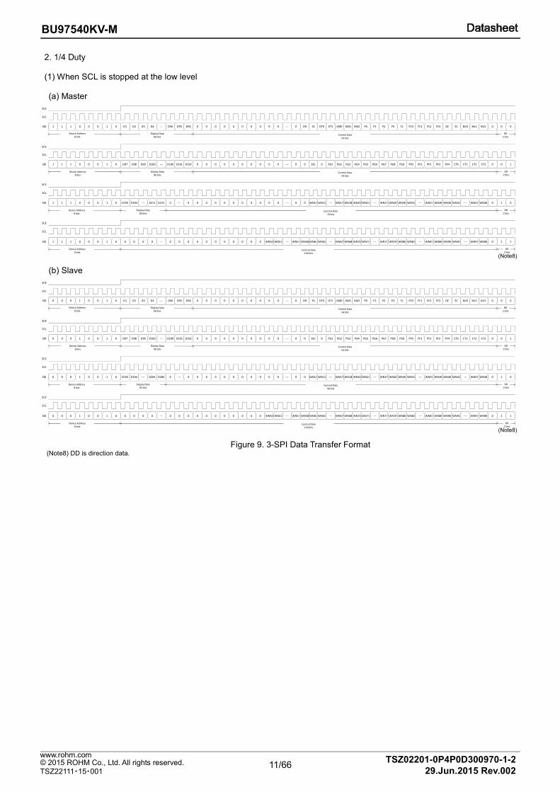
Figure 9. 3-SPI Data Transfer Format (Note8) DD is direction data.
(Note8)
(Note8)
12/66
BU97540KV-M
TSZ02201-0P4P0D300970-1-2 © 2015 ROHM Co., Ltd. All rights reserved. 29.Jun.2015 Rev.002
www.rohm.com
TSZ22111・15・001
(2) When SCL is stopped at the high level (a) Master
SCE
SCL
SDI 1 1 1 0 0 0 1 0 D1 D2 D3 D4 --- D94 D95 D96 0 0 0 0 0 0 0 0 0 0 --- 0 DR SS DT0 DT1 KM0 KM1 KM2 P0 P1 P2 P3 FL FC0 FC1 FC2 FC3 OC SC BU0 BU1 BU2 0 0 0
SCE
SCL
SDI 1 1 1 0 0 0 1 0 D97 D98 D99 D100 --- D190 D191 D192 0 0 0 0 0 0 0 0 0 0 --- 0 0 SSC 0 PG1 PG2 PG3 PG4 PG5 CT1 CT2PG6 PG7 PG8 PG9 PF0 PF1 CT3 0 0 1
SCE
SCL
PF2 PF3 PF4 CT0
SDI 1 1 1 0 0 0 1 0 D193 D194 --- D271 D272 0 --- 0 0 0 0 0 0 0 0 0 0 0 --- 0 0 WN10 WN11 --- WN17 WN18 WN20 WN41 ---WN21 --- WN27 WN28 WN30 WN31 WN47 WN48 0 1 0
SCE
--- WN37 WN38 WN40
SCL
SDI 1 1 1 0 0 0 1 0 0 0 0 0 --- 0 0 0 0 0 0 0 0 0 0 0 WN50 WN51 --- WN57 WN58 WN60 WN61 --- WN67 WN68 WN70 WN71 --- WN77 WN78 WN80 WN81 --- WN87 WN88 WN90 WN91 --- WN97 WN98 0 1 1
DD2 bits
Display Data96 bits
Device Address8 bits
Device Address8 bits
Display Data96 bits
DD2 bits
Device Address8 bits
DD2 bits
Device Address8 bits
DD2 bits
Control Data54 bits
Control Data54 bits
Control Data150 bits
Display Data80 bits
Control Data70 bits
(b) Slave
SCE
SCL
SDI 0 0 0 1 0 0 1 0 D1 D2 D3 D4 --- D94 D95 D96 0 0 0 0 0 0 0 0 0 0 --- 0 DR SS DT0 DT1 KM0 KM1 KM2 P0 P1 P2 P3 FL FC0 FC1 FC2 FC3 OC SC BU0 BU1 BU2 0 0 0
SCE
SCL
SDI 0 0 0 1 0 0 1 0 D97 D98 D99 D100 --- D190 D191 D192 0 0 0 0 0 0 0 0 0 0 --- 0 0 SSC 0 PG1 PG2 PG3 PG4 PG5 CT1 CT2PG6 PG7 PG8 PG9 PF0 PF1 CT3 0 0 1
SCE
SCL
PF2 PF3 PF4 CT0
SDI 0 0 0 1 0 0 1 0 D193 D194 --- D283 D284 0 --- 0 0 0 0 0 0 0 0 0 0 0 --- 0 0 WN10 WN11 --- WN17 WN18 WN20 WN41 ---WN21 --- WN27 WN28 WN30 WN31 WN47 WN48 0 1 0
SCE
--- WN37 WN38 WN40
SCL
SDI 0 0 0 1 0 0 1 0 0 0 0 0 --- 0 0 0 0 0 0 0 0 0 0 0 WN50 WN51 --- WN57 WN58 WN60 WN61 --- WN67 WN68 WN70 WN71 --- WN77 WN78 WN80 WN81 --- WN87 WN88 WN90 WN91 --- WN97 WN98 0 1 1
DD2 bits
Display Data96 bits
Device Address8 bits
Device Address8 bits
Display Data96 bits
DD2 bits
Device Address8 bits
DD2 bits
Device Address8 bits
DD2 bits
Control Data54 bits
Control Data54 bits
Control Data150 bits
Display Data92 bits
Control Data58 bits
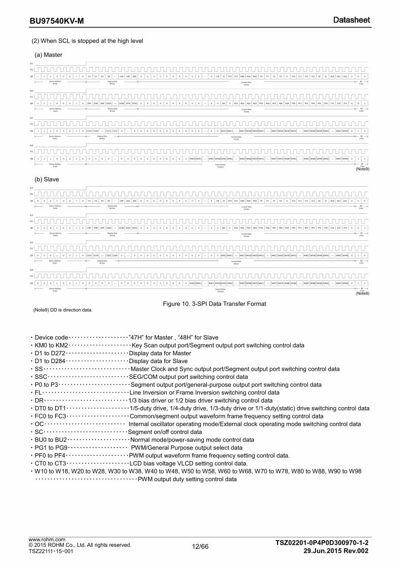
Figure 10. 3-SPI Data Transfer Format (Note9) DD is direction data.
・Device code・・・・・・・・・・・・・・・・・・・・”47H” for Master , “48H” for Slave
・KM0 to KM2・・・・・・・・・・・・・・・・・・・・・Key Scan output port/Segment output port switching control data
・D1 to D272・・・・・・・・・・・・・・・・・・・・・Display data for Master
・D1 to D284・・・・・・・・・・・・・・・・・・・・・Display data for Slave
・SS・・・・・・・・・・・・・・・・・・・・・・・・・・・・・Master Clock and Sync output port/Segment output port switching control data
・SSC・・・・・・・・・・・・・・・・・・・・・・・・・・・SEG/COM output port switching control data
・P0 to P3・・・・・・・・・・・・・・・・・・・・・・・・Segment output port/general-purpose output port switching control data
・FL・・・・・・・・・・・・・・・・・・・・・・・・・・・・・Line Inversion or Frame Inversion switching control data
・DR・・・・・・・・・・・・・・・・・・・・・・・・・・・・1/3 bias driver or 1/2 bias driver switching control data
・DT0 to DT1・・・・・・・・・・・・・・・・・・・・・1/5-duty drive, 1/4-duty drive, 1/3-duty drive or 1/1-duty(static) drive switching control data
・FC0 to FC3・・・・・・・・・・・・・・・・・・・・・Common/segment output waveform frame frequency setting control data
・OC・・・・・・・・・・・・・・・・・・・・・・・・・・・ Internal oscillator operating mode/External clock operating mode switching control data
・SC・・・・・・・・・・・・・・・・・・・・・・・・・・・・Segment on/off control data
・BU0 to BU2・・・・・・・・・・・・・・・・・・・・・Normal mode/power-saving mode control data
・PG1 to PG9・・・・・・・・・・・・・・・・・・・・ PWM/General Purpose output select data
・PF0 to PF4・・・・・・・・・・・・・・・・・・・・・PWM output waveform frame frequency setting control data.
・CT0 to CT3・・・・・・・・・・・・・・・・・・・・・LCD bias voltage VLCD setting control data.
・W10 to W18, W20 to W28, W30 to W38, W40 to W48, W50 to W58, W60 to W68, W70 to W78, W80 to W88, W90 to W98
・・・・・・・・・・・・・・・・・・・・・・・・・・・・・・・・・・PWM output duty setting control data
(Note9)
(Note9)
13/66
BU97540KV-M
TSZ02201-0P4P0D300970-1-2 © 2015 ROHM Co., Ltd. All rights reserved. 29.Jun.2015 Rev.002
www.rohm.com
TSZ22111・15・001
3. 1/3 Duty (1) When SCL is stopped at the low level
(a) Master
D3 D41 1 1 0 0 0 --- D94 D95 D96 0
SCL
1 0 D1 D2 0 0 0 0 0 0 0 0 0 --- 0 DR SS DT0 DT1 KM0 KM1 KM2 P0 P1 P2 P3 FL FC0 FC1 FC2 FC3 OC SC BU0 BU1 BU2 0 0 0
1 1 1 0 0 D192 00 1 0 D97 D98 D99 0 0 0 0 0
SCE
D100 --- D190 D191 0 0 0 0 --- 0 PG8 PG9RF SSC 0 PG1 PG2 PG3 1PF0 PF1 PF2 PF3 PF4 CT0
0
CT1 CT2 CT3 0 0PG4 PG5 PG6 PG7
0 D193 D194 --- D2031 1 1 0 0 D204 0 --- 0 0
SDI
SCE
SCL
SDI 1 0 0 0 0 0 0 0 0 0 --- 0 0 WN10 WN11 --- WN17 WN18 WN20 WN21 --- WN27 WN28 WN30 WN31 --- WN37 WN38 WN40 WN41 --- WN47 WN48 0 1 0
1 1 1 0 0 0 1 0 0 0 0 0 --- 0 0 0 0 0 0 0 0 0
SCE
SCL
SDI
SCE
SCL
0 0 WN50 WN51 --- WN57 WN78 WN80WN58 WN60 WN61 --- WN67 WN68 1WN81 --- WN87 WN88 WN90 WN91SDI --- WN97 WN98 0 1WN70 WN71 --- WN77
DD2 bits
Display Data96 bits
Device Address8 bits
Device Address8 bits
Display Data96 bits
DD2 bits
Device Address8 bits
DD2 bits
Device Address8 bits
DD2 bits
Control Data54 bits
Control Data54 bits
Control Data150 bits
Display Data12 bits
Control Data138 bits
(b) Slave
SCE
SCL
SDI 0 0 0 1 0 0 1 0 D1 D2 D3 D4 --- D94 D95 D96 0 0 0 0 0 0 0 0 0 0 --- 0 DR SS DT0 DT1 KM0 KM1 KM2 P0 P1 P2 P3 FL FC0 FC1 FC2 FC3 OC SC BU0 BU1 BU2 0 0 0
SCE
SCL
SDI 0 0 0 1 0 0 1 0 D97 D98 D99 D100 --- D190 D191 D192 0 0 0 0 0 0 0 0 0 0 --- 0 0 SSC 0 PG1 PG2 PG3 PG4 PG5 CT1 CT2PG6 PG7 PG8 PG9 PF0 PF1 CT3 0 0 1
SCE
SCL
PF2 PF3 PF4 CT0
SDI 0 0 0 1 0 0 1 0 D193 D194 --- D212 D213 0 --- 0 0 0 0 0 0 0 0 0 0 0 --- 0 0 WN10 WN11 --- WN17 WN18 WN20 WN41 ---WN21 --- WN27 WN28 WN30 WN31 WN47 WN48 0 1 0
SCE
--- WN37 WN38 WN40
SCL
SDI 0 0 0 1 0 0 1 0 0 0 0 0 --- 0 0 0 0 0 0 0 0 0 0 0 WN50 WN51 --- WN57 WN58 WN60 WN61 --- WN67 WN68 WN70 WN71 --- WN77 WN78 WN80 WN81 --- WN87 WN88 WN90 WN91 --- WN97 WN98 0 1 1
DD2 bits
Display Data96 bits
Device Address8 bits
Device Address8 bits
Display Data96 bits
DD2 bits
Device Address8 bits
DD2 bits
Device Address8 bits
DD2 bits
Control Data54 bits
Control Data54 bits
Control Data150 bits
Display Data21 bits
Control Data129 bits
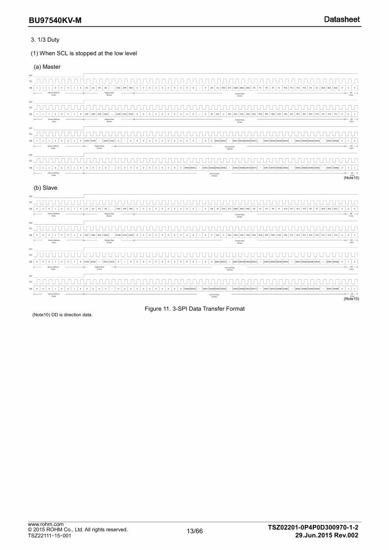
Figure 11. 3-SPI Data Transfer Format (Note10) DD is direction data.
(Note10)
(Note10)
14/66
BU97540KV-M
TSZ02201-0P4P0D300970-1-2 © 2015 ROHM Co., Ltd. All rights reserved. 29.Jun.2015 Rev.002
www.rohm.com
TSZ22111・15・001
(2) When SCL is stopped at the high level
(a) Master
SCE
SCL
SDI 1 1 1 0 0 0 1 0 D1 D2 D3 D4 --- D94 D95 D96 0 0 0 0 0 0 0 0 0 0 --- 0 DR SS DT0 DT1 KM0 KM1 KM2 P0 P1 P2 P3 FL FC0 FC1 FC2 FC3 OC SC BU0 BU1 BU2 0 0 0
SCE
SCL
SDI 1 1 1 0 0 0 1 0 D97 D98 D99 D100 --- D190 D191 D192 0 0 0 0 0 0 0 0 0 0 --- 0 0 SSC 0 PG1 PG2 PG3 PG4 PG5 CT1 CT2PG6 PG7 PG8 PG9 PF0 PF1 CT3 0 0 1
SCE
SCL
PF2 PF3 PF4 CT0
SDI 1 1 1 0 0 0 1 0 D193 D194 --- D203 D204 0 --- 0 0 0 0 0 0 0 0 0 0 0 --- 0 0 WN10 WN11 --- WN17 WN18 WN20 WN41 ---WN21 --- WN27 WN28 WN30 WN31 WN47 WN48 0 1 0
SCE
--- WN37 WN38 WN40
SCL
SDI 1 1 1 0 0 0 1 0 0 0 0 0 --- 0 0 0 0 0 0 0 0 0 0 0 WN50 WN51 --- WN57 WN58 WN60 WN61 --- WN67 WN68 WN70 WN71 --- WN77 WN78 WN80 WN81 --- WN87 WN88 WN90 WN91 --- WN97 WN98 0 1 1
DD2 bits
Display Data96 bits
Device Address8 bits
Device Address8 bits
Display Data96 bits
DD2 bits
Device Address8 bits
DD2 bits
Device Address8 bits
DD2 bits
Control Data54 bits
Control Data54 bits
Control Data150 bits
Display Data12 bits
Control Data138 bits
(b) Slave
SCE
SCL
SDI 0 0 0 1 0 0 1 0 D1 D2 D3 D4 --- D94 D95 D96 0 0 0 0 0 0 0 0 0 0 --- 0 DR SS DT0 DT1 KM0 KM1 KM2 P0 P1 P2 P3 FL FC0 FC1 FC2 FC3 OC SC BU0 BU1 BU2 0 0 0
SCE
SCL
SDI 0 0 0 1 0 0 1 0 D97 D98 D99 D100 --- D190 D191 D192 0 0 0 0 0 0 0 0 0 0 --- 0 0 SSC 0 PG1 PG2 PG3 PG4 PG5 CT1 CT2PG6 PG7 PG8 PG9 PF0 PF1 CT3 0 0 1
SCE
SCL
PF2 PF3 PF4 CT0
SDI 0 0 0 1 0 0 1 0 D193 D194 --- D212 D213 0 --- 0 0 0 0 0 0 0 0 0 0 0 --- 0 0 WN10 WN11 --- WN17 WN18 WN20 WN41 ---WN21 --- WN27 WN28 WN30 WN31 WN47 WN48 0 1 0
SCE
--- WN37 WN38 WN40
SCL
SDI 0 0 0 1 0 0 1 0 0 0 0 0 --- 0 0 0 0 0 0 0 0 0 0 0 WN50 WN51 --- WN57 WN58 WN60 WN61 --- WN67 WN68 WN70 WN71 --- WN77 WN78 WN80 WN81 --- WN87 WN88 WN90 WN91 --- WN97 WN98 0 1 1
DD2 bits
Display Data96 bits
Device Address8 bits
Device Address8 bits
Display Data96 bits
DD2 bits
Device Address8 bits
DD2 bits
Device Address8 bits
DD2 bits
Control Data54 bits
Control Data54 bits
Control Data150 bits
Display Data21 bits
Control Data129 bits
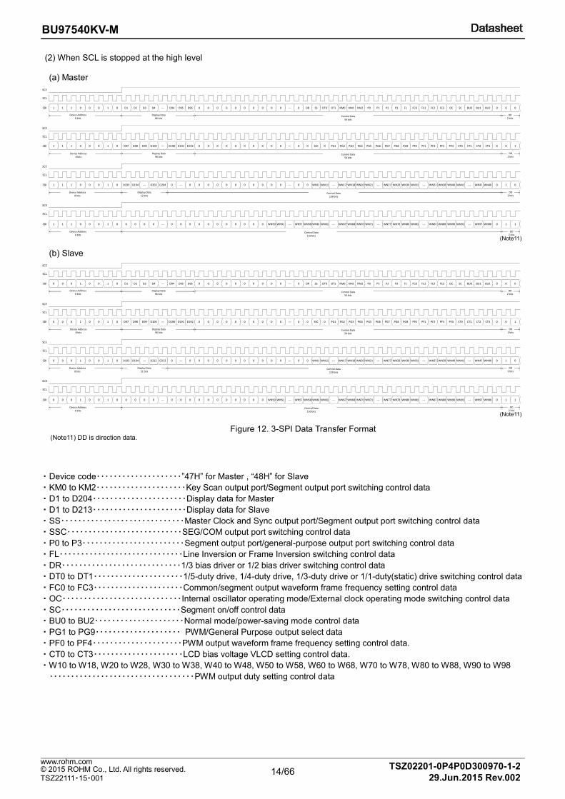
Figure 12. 3-SPI Data Transfer Format (Note11) DD is direction data.
・Device code・・・・・・・・・・・・・・・・・・・・”47H” for Master , “48H” for Slave
・KM0 to KM2・・・・・・・・・・・・・・・・・・・・・Key Scan output port/Segment output port switching control data
・D1 to D204・・・・・・・・・・・・・・・・・・・・・・Display data for Master
・D1 to D213・・・・・・・・・・・・・・・・・・・・・・Display data for Slave
・SS・・・・・・・・・・・・・・・・・・・・・・・・・・・・・Master Clock and Sync output port/Segment output port switching control data
・SSC・・・・・・・・・・・・・・・・・・・・・・・・・・・SEG/COM output port switching control data
・P0 to P3・・・・・・・・・・・・・・・・・・・・・・・・Segment output port/general-purpose output port switching control data
・FL・・・・・・・・・・・・・・・・・・・・・・・・・・・・・Line Inversion or Frame Inversion switching control data
・DR・・・・・・・・・・・・・・・・・・・・・・・・・・・・1/3 bias driver or 1/2 bias driver switching control data
・DT0 to DT1・・・・・・・・・・・・・・・・・・・・・1/5-duty drive, 1/4-duty drive, 1/3-duty drive or 1/1-duty(static) drive switching control data
・FC0 to FC3・・・・・・・・・・・・・・・・・・・・・Common/segment output waveform frame frequency setting control data
・OC・・・・・・・・・・・・・・・・・・・・・・・・・・・・Internal oscillator operating mode/External clock operating mode switching control data
・SC・・・・・・・・・・・・・・・・・・・・・・・・・・・・Segment on/off control data
・BU0 to BU2・・・・・・・・・・・・・・・・・・・・・Normal mode/power-saving mode control data
・PG1 to PG9・・・・・・・・・・・・・・・・・・・・ PWM/General Purpose output select data
・PF0 to PF4・・・・・・・・・・・・・・・・・・・・・PWM output waveform frame frequency setting control data.
・CT0 to CT3・・・・・・・・・・・・・・・・・・・・・LCD bias voltage VLCD setting control data.
・W10 to W18, W20 to W28, W30 to W38, W40 to W48, W50 to W58, W60 to W68, W70 to W78, W80 to W88, W90 to W98
・・・・・・・・・・・・・・・・・・・・・・・・・・・・・・・・・・PWM output duty setting control data
(Note11)
(Note11)
15/66
BU97540KV-M
TSZ02201-0P4P0D300970-1-2 © 2015 ROHM Co., Ltd. All rights reserved. 29.Jun.2015 Rev.002
www.rohm.com
TSZ22111・15・001
4. 1/1 Duty (Static) (1) When SCL is stopped at the low level
(a) Master
1 1 1 0 0 0 1 0 D1 D2 D3 D4 --- D66 D67 D68 0 0 0 0 0 0 0 0 0 0 --- 0 DR SS DT0 DT1 KM0 KM1 KM2 P0 P1 P2 P3 FL FC0 FC1 FC2 FC3 OC SC BU0 BU1 BU2 0 0 0
1 1 1 0 0 0 1 0 0 0 0 0 --- 0 0 0 0 0 0 0 0 0 0 0 0 0 --- 0 0 SSC 0 PG1 PG2 PG3 PG4 PG5 PG6 PG7 PG8 PG9 PF0 PF1 PF2 PF3 PF4 CT0 CT1 CT2 CT3 0 0 1
1 1 1 0 0 0 1 0 0 0 0 0 --- 0 0 0 0 0 0 0 0 0 0 0 0 0 --- 0 0 WN10 WN11 --- WN17 WN18 WN20 WN21 --- WN27 WN28 WN30 WN31 --- WN37 WN38 WN40 WN41 --- WN47 WN48 0 1 0
1 1 1 0 0 0 1 0 0 0 0 0 --- 0 0 0 0 0 0 0 0 0 0 0 WN50 WN51 --- WN57 WN58 WN60 WN61 --- WN67 WN68 WN70 WN71 --- WN77 WN78 WN80 WN81 --- WN87 WN88 WN90 WN91 --- WN97 WN98 0 1 1
SCE
SCL
SDI
SCE
SCL
SDI
SCE
SCL
SDI
SCE
SCL
SDI
DD2 bits
Display Data68 bits
Device Address8 bits
Device Address8 bits
DD2 bits
Device Address8 bits
DD2 bits
Device Address8 bits
DD2 bits
Control Data82 bits
Control Data150 bits
Control Data150 bits
Control Data150 bits
(b) Slave
SCE
SCL
SDI 0 0 0 1 0 0 1 0 D1 D2 D3 D4 --- D69 D70 D71 0 0 0 0 0 0 0 0 0 0 --- 0 DR SS DT0 DT1 KM0 KM1 KM2 P0 P1 P2 P3 FL FC0 FC1 FC2 FC3 OC SC BU0 BU1 BU2 0 0 0
SCE
SCL
SDI 0 0 0 1 0 0 1 0 0 0 0 0 --- 0 0 0 0 0 0 0 0 0 0 0 0 0 --- 0 0 SSC 0 PG1 PG2 PG3 PG4 PG5 CT1 CT2PG6 PG7 PG8 PG9 PF0 PF1 CT3 0 0 1
SCE
SCL
PF2 PF3 PF4 CT0
SDI 0 0 0 1 0 0 1 0 0 0 0 0 --- 0 0 0 0 0 0 0 0 0 0 0 0 0 --- 0 0 WN10 WN11 --- WN17 WN18 WN20 WN41 ---WN21 --- WN27 WN28 WN30 WN31 WN47 WN48 0 1 0
SCE
--- WN37 WN38 WN40
SCL
SDI 0 0 0 1 0 0 1 0 0 0 0 0 --- 0 0 0 0 0 0 0 0 0 0 0 WN50 WN51 --- WN57 WN58 WN60 WN61 --- WN67 WN68 WN70 WN71 --- WN77 WN78 WN80 WN81 --- WN87 WN88 WN90 WN91 --- WN97 WN98 0 1 1
DD2 bits
Display Data71 bits
Device Address8 bits
Device Address8 bits
DD2 bits
Device Address8 bits
DD2 bits
Device Address8 bits
DD2 bits
Control Data79 bits
Control Data150 bits
Control Data150 bits
Control Data150 bits
Figure 13. 3-SPI Data Transfer Format (Note12) DD is direction data.
(Note12)
(Note12)

16/66
BU97540KV-M
TSZ02201-0P4P0D300970-1-2 © 2015 ROHM Co., Ltd. All rights reserved. 29.Jun.2015 Rev.002
www.rohm.com
TSZ22111・15・001
(2) When SCL is stopped at the high level
(a) Master
SCE
SCL
SDI 1 1 1 0 0 0 1 0 D1 D2 D3 D4 --- D66 D67 D68 0 0 0 0 0 0 0 0 0 0 --- 0 DR SS DT0 DT1 KM0 KM1 KM2 P0 P1 P2 P3 FL FC0 FC1 FC2 FC3 OC SC BU0 BU1 BU2 0 0 0
SCE
SCL
SDI 1 1 1 0 0 0 1 0 0 0 0 0 --- 0 0 0 0 0 0 0 0 0 0 0 0 0 --- 0 0 SSC 0 PG1 PG2 PG3 PG4 PG5 CT1 CT2PG6 PG7 PG8 PG9 PF0 PF1 CT3 0 0 1
SCE
SCL
PF2 PF3 PF4 CT0
SDI 1 1 1 0 0 0 1 0 0 0 0 0 --- 0 0 0 0 0 0 0 0 0 0 0 0 0 --- 0 0 WN10 WN11 --- WN17 WN18 WN20 WN41 ---WN21 --- WN27 WN28 WN30 WN31 WN47 WN48 0 1 0
SCE
--- WN37 WN38 WN40
SCL
SDI 1 1 1 0 0 0 1 0 0 0 0 0 --- 0 0 0 0 0 0 0 0 0 0 0 WN50 WN51 --- WN57 WN58 WN60 WN61 --- WN67 WN68 WN70 WN71 --- WN77 WN78 WN80 WN81 --- WN87 WN88 WN90 WN91 --- WN97 WN98 0 1 1
DD2 bits
Display Data68 bits
Device Address8 bits
Device Address8 bits
DD2 bits
Device Address8 bits
DD2 bits
Device Address8 bits
DD2 bits
Control Data82 bits
Control Data150 bits
Control Data150 bits
Control Data150 bits
(b) Slave
SCE
SCL
SDI 0 0 0 1 0 0 1 0 D1 D2 D3 D4 --- D69 D70 D71 0 0 0 0 0 0 0 0 0 0 --- 0 DR SS DT0 DT1 KM0 KM1 KM2 P0 P1 P2 P3 FL FC0 FC1 FC2 FC3 OC SC BU0 BU1 BU2 0 0 0
SCE
SCL
SDI 0 0 0 1 0 0 1 0 0 0 0 0 --- 0 0 0 0 0 0 0 0 0 0 0 0 0 --- 0 0 SSC 0 PG1 PG2 PG3 PG4 PG5 CT1 CT2PG6 PG7 PG8 PG9 PF0 PF1 CT3 0 0 1
SCE
SCL
PF2 PF3 PF4 CT0
SDI 0 0 0 1 0 0 1 0 0 0 0 0 --- 0 0 0 0 0 0 0 0 0 0 0 0 0 --- 0 0 WN10 WN11 --- WN17 WN18 WN20 WN41 ---WN21 --- WN27 WN28 WN30 WN31 WN47 WN48 0 1 0
SCE
--- WN37 WN38 WN40
SCL
SDI 0 0 0 1 0 0 1 0 0 0 0 0 --- 0 0 0 0 0 0 0 0 0 0 0 WN50 WN51 --- WN57 WN58 WN60 WN61 --- WN67 WN68 WN70 WN71 --- WN77 WN78 WN80 WN81 --- WN87 WN88 WN90 WN91 --- WN97 WN98 0 1 1
DD2 bits
Display Data71 bits
Device Address8 bits
Device Address8 bits
DD2 bits
Device Address8 bits
DD2 bits
Device Address8 bits
DD2 bits
Control Data79 bits
Control Data150 bits
Control Data150 bits
Control Data150 bits
Figure 14. 3-SPI Data Transfer Format (Note13) DD is direction data.
・Device code・・・・・・・・・・・・・・・・・・・・”47H” for Master , “48H” for Slave
・KM0 to KM2・・・・・・・・・・・・・・・・・・・・・Key Scan output port/Segment output port switching control data
・D1 to D68・・・・・・・・・・・・・・・・・・・・・・・Display data for Master
・D1 to D71・・・・・・・・・・・・・・・・・・・・・・・Display data for Slave
・SS・・・・・・・・・・・・・・・・・・・・・・・・・・・・・Master Clock and Sync output port/Segment output port switching control data
・SSC・・・・・・・・・・・・・・・・・・・・・・・・・・・SEG/COM output port switching control data
・P0 to P3・・・・・・・・・・・・・・・・・・・・・・・・Segment output port/general-purpose output port switching control data
・FL・・・・・・・・・・・・・・・・・・・・・・・・・・・・・Line Inversion or Frame Inversion switching control data
・DR・・・・・・・・・・・・・・・・・・・・・・・・・・・・1/3 bias driver or 1/2 bias driver switching control data
・DT0 to DT1・・・・・・・・・・・・・・・・・・・・・1/5-duty drive, 1/4-duty drive, 1/3-duty drive or 1/1-duty(static) drive switching control data
・FC0 to FC3・・・・・・・・・・・・・・・・・・・・・Common/segment output waveform frame frequency setting control data
・OC・・・・・・・・・・・・・・・・・・・・・・・・・・・ Internal oscillator operating mode/External clock operating mode switching control data
・SC・・・・・・・・・・・・・・・・・・・・・・・・・・・・Segment on/off control data
・BU0 to BU2・・・・・・・・・・・・・・・・・・・・・Normal mode/power-saving mode control data
・PG1 to PG9・・・・・・・・・・・・・・・・・・・・ PWM/General Purpose output select data
・PF0 to PF4・・・・・・・・・・・・・・・・・・・・・PWM output waveform frame frequency setting control data.
・CT0 to CT3・・・・・・・・・・・・・・・・・・・・・LCD bias voltage VLCD setting control data.
・W10 to W18, W20 to W28, W30 to W38, W40 to W48, W50 to W58, W60 to W68, W70 to W78, W80 to W88, W90 to W98
・・・・・・・・・・・・・・・・・・・・・・・・・・・・・・・・・・PWM output duty setting control data
(Note13)
(Note13)
17/66
BU97540KV-M
TSZ02201-0P4P0D300970-1-2 © 2015 ROHM Co., Ltd. All rights reserved. 29.Jun.2015 Rev.002
www.rohm.com
TSZ22111・15・001
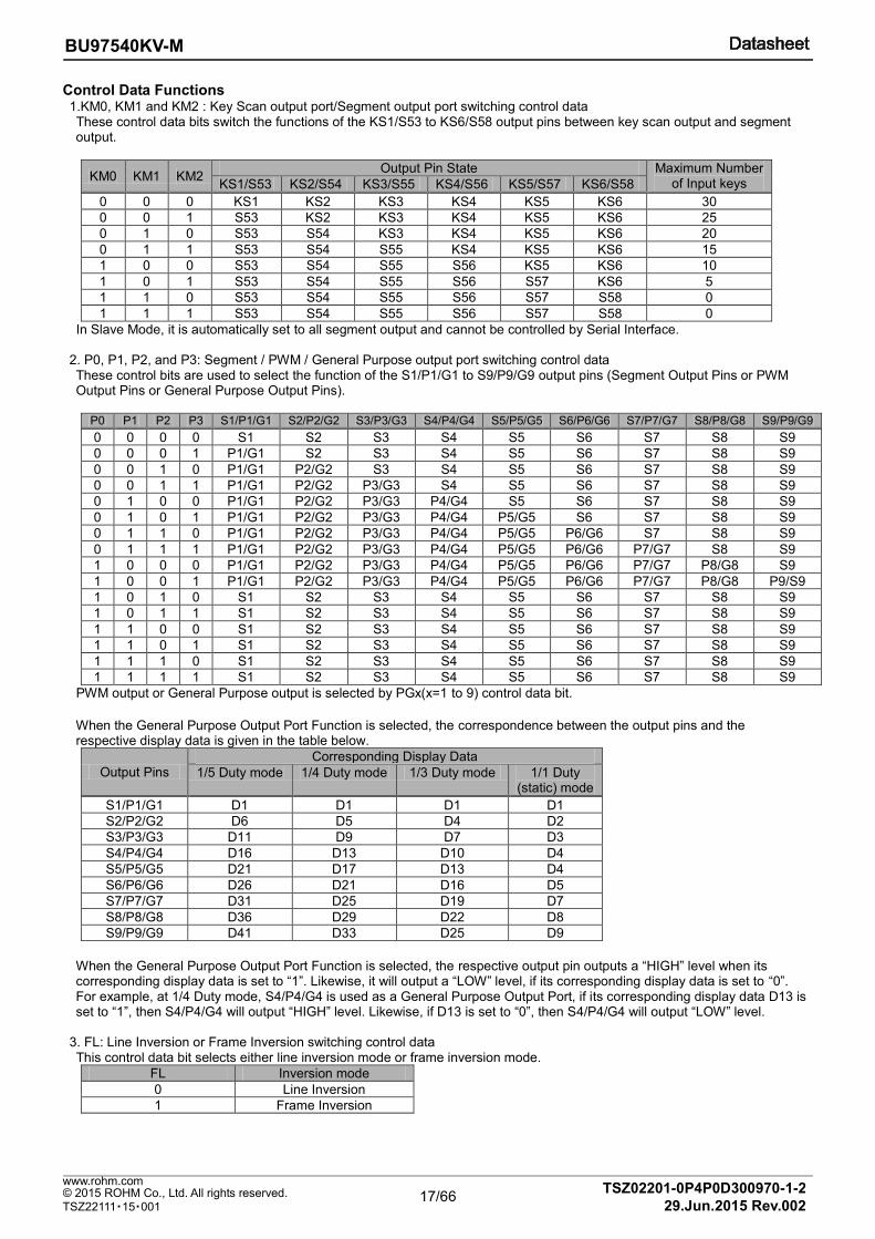
Control Data Functions 1.KM0, KM1 and KM2 : Key Scan output port/Segment output port switching control data
These control data bits switch the functions of the KS1/S53 to KS6/S58 output pins between key scan output and segment output.
KM0 KM1 KM2 Output Pin State Maximum Number
of Input keys KS1/S53 KS2/S54 KS3/S55 KS4/S56 KS5/S57 KS6/S58
0 0 0 KS1 KS2 KS3 KS4 KS5 KS6 30
0 0 1 S53 KS2 KS3 KS4 KS5 KS6 25
0 1 0 S53 S54 KS3 KS4 KS5 KS6 20
0 1 1 S53 S54 S55 KS4 KS5 KS6 15
1 0 0 S53 S54 S55 S56 KS5 KS6 10
1 0 1 S53 S54 S55 S56 S57 KS6 5
1 1 0 S53 S54 S55 S56 S57 S58 0
1 1 1 S53 S54 S55 S56 S57 S58 0
In Slave Mode, it is automatically set to all segment output and cannot be controlled by Serial Interface. 2. P0, P1, P2, and P3: Segment / PWM / General Purpose output port switching control data These control bits are used to select the function of the S1/P1/G1 to S9/P9/G9 output pins (Segment Output Pins or PWM Output Pins or General Purpose Output Pins).
P0 P1 P2 P3 S1/P1/G1 S2/P2/G2 S3/P3/G3 S4/P4/G4 S5/P5/G5 S6/P6/G6 S7/P7/G7 S8/P8/G8 S9/P9/G9
0 0 0 0 S1 S2 S3 S4 S5 S6 S7 S8 S9
0 0 0 1 P1/G1 S2 S3 S4 S5 S6 S7 S8 S9
0 0 1 0 P1/G1 P2/G2 S3 S4 S5 S6 S7 S8 S9
0 0 1 1 P1/G1 P2/G2 P3/G3 S4 S5 S6 S7 S8 S9
0 1 0 0 P1/G1 P2/G2 P3/G3 P4/G4 S5 S6 S7 S8 S9
0 1 0 1 P1/G1 P2/G2 P3/G3 P4/G4 P5/G5 S6 S7 S8 S9
0 1 1 0 P1/G1 P2/G2 P3/G3 P4/G4 P5/G5 P6/G6 S7 S8 S9
0 1 1 1 P1/G1 P2/G2 P3/G3 P4/G4 P5/G5 P6/G6 P7/G7 S8 S9
1 0 0 0 P1/G1 P2/G2 P3/G3 P4/G4 P5/G5 P6/G6 P7/G7 P8/G8 S9
1 0 0 1 P1/G1 P2/G2 P3/G3 P4/G4 P5/G5 P6/G6 P7/G7 P8/G8 P9/S9
1 0 1 0 S1 S2 S3 S4 S5 S6 S7 S8 S9
1 0 1 1 S1 S2 S3 S4 S5 S6 S7 S8 S9
1 1 0 0 S1 S2 S3 S4 S5 S6 S7 S8 S9
1 1 0 1 S1 S2 S3 S4 S5 S6 S7 S8 S9
1 1 1 0 S1 S2 S3 S4 S5 S6 S7 S8 S9
1 1 1 1 S1 S2 S3 S4 S5 S6 S7 S8 S9
PWM output or General Purpose output is selected by PGx(x=1 to 9) control data bit.
When the General Purpose Output Port Function is selected, the correspondence between the output pins and the respective display data is given in the table below.
Output Pins
Corresponding Display Data
1/5 Duty mode 1/4 Duty mode 1/3 Duty mode 1/1 Duty (static) mode
S1/P1/G1 D1 D1 D1 D1
S2/P2/G2 D6 D5 D4 D2
S3/P3/G3 D11 D9 D7 D3
S4/P4/G4 D16 D13 D10 D4
S5/P5/G5 D21 D17 D13 D4
S6/P6/G6 D26 D21 D16 D5
S7/P7/G7 D31 D25 D19 D7
S8/P8/G8 D36 D29 D22 D8
S9/P9/G9 D41 D33 D25 D9
When the General Purpose Output Port Function is selected, the respective output pin outputs a “HIGH” level when its corresponding display data is set to “1”. Likewise, it will output a “LOW” level, if its corresponding display data is set to “0”. For example, at 1/4 Duty mode, S4/P4/G4 is used as a General Purpose Output Port, if its corresponding display data D13 is set to “1”, then S4/P4/G4 will output “HIGH” level. Likewise, if D13 is set to “0”, then S4/P4/G4 will output “LOW” level.
3. FL: Line Inversion or Frame Inversion switching control data
This control data bit selects either line inversion mode or frame inversion mode.
FL Inversion mode
0 Line Inversion
1 Frame Inversion
18/66
BU97540KV-M
TSZ02201-0P4P0D300970-1-2 © 2015 ROHM Co., Ltd. All rights reserved. 29.Jun.2015 Rev.002
www.rohm.com
TSZ22111・15・001
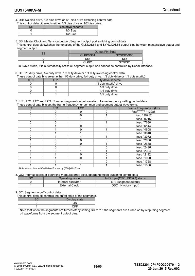
4. DR: 1/3 bias drive, 1/2 bias drive or 1/1 bias drive switching control data This control data bit selects either 1/3 bias drive or 1/2 bias drive.
DR Bias drive scheme
0 1/3 Bias
1 1/2 Bias
5. SS: Master Clock and Sync output port/Segment output port switching control data
This control data bit switches the functions of the CLKIO/S64 and SYNCIO/S65 output pins between master/slave output and segment output.
SS Output Pin State
CLKIO/S64 SYNCIO/S65
0 S64 S65
1 CLKIO SYNCIO
In Slave Mode, it is automatically set to all segment output and cannot be controlled by Serial Interface.
6. DT: 1/5 duty drive, 1/4 duty drive, 1/3 duty drive or 1/1 duty switching control data These control data bits select either 1/5 duty drive, 1/4 duty drive, 1/3 duty drive or 1/1 duty (static)
DT0 DT1 Duty drive scheme
0 0 1/1 duty (static) drive
0 0 1/3 duty drive
0 1 1/4 duty drive
1 1 1/5 duty drive
7. FC0, FC1, FC2 and FC3: Common/segment output waveform frame frequency setting control data These control data bits set the frame frequency for common and segment output waveforms.
FC0 FC1 FC2 FC3 Frame Frequency fo(Hz)
0 0 0 0 fosc(Note14)
/ 12288
0 0 0 1 fosc / 10752
0 0 1 0 fosc / 9216
0 0 1 1 fosc / 7680
0 1 0 0 fosc / 6144
0 1 0 1 fosc / 4608
0 1 1 0 fosc / 3840
0 1 1 1 fosc / 3072
1 0 0 0 fosc / 2880
1 0 0 1 fosc / 2688
1 0 1 0 fosc / 2496
1 0 1 1 fosc / 2304
1 1 0 0 fosc / 2112
1 1 0 1 fosc / 1920
1 1 1 0 fosc / 1728
1 1 1 1 fosc / 1536 (Note14)fosc: Internal Oscillation Frequency (600 [kHz] Typ)
8. OC: Internal oscillator operating mode/External clock operating mode switching control data
OC Operating mode In/Out pin(OSC_IN/S73) status
0 Internal oscillator S73 (segment output)
1 External Clock OSC_IN (clock input)
9. SC: Segment on/off control data This control data bit controls the on/off state of the segments.
SC Display state
0 ON
1 OFF
Note that when the segments are turned off by setting SC to “1”, the segments are turned off by outputting segment off waveforms from the segment output pins.
19/66
BU97540KV-M
TSZ02201-0P4P0D300970-1-2 © 2015 ROHM Co., Ltd. All rights reserved. 29.Jun.2015 Rev.002
www.rohm.com
TSZ22111・15・001
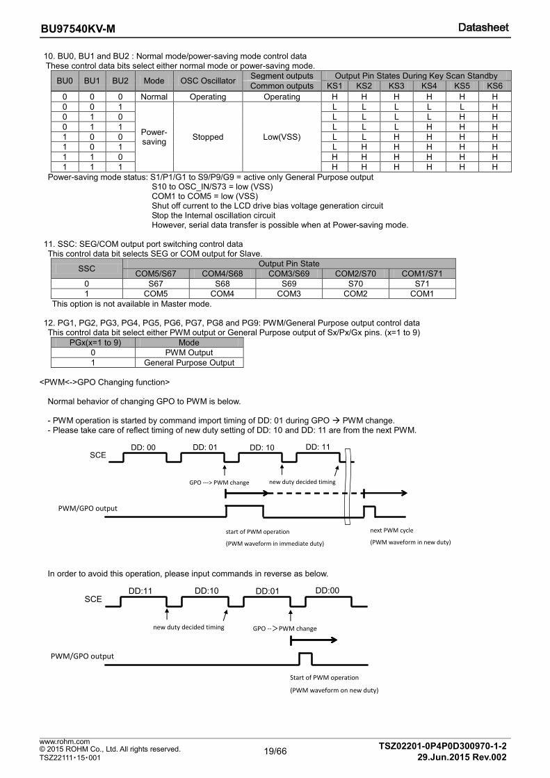
10. BU0, BU1 and BU2 : Normal mode/power-saving mode control data These control data bits select either normal mode or power-saving mode.
BU0 BU1 BU2 Mode OSC Oscillator Segment outputs Output Pin States During Key Scan Standby
Common outputs KS1 KS2 KS3 KS4 KS5 KS6
0 0 0 Normal Operating Operating H H H H H H
0 0 1
Power-saving
Stopped Low(VSS)
L L L L L H
0 1 0 L L L L H H
0 1 1 L L L H H H
1 0 0 L L H H H H
1 0 1 L H H H H H
1 1 0 H H H H H H
1 1 1 H H H H H H
Power-saving mode status: S1/P1/G1 to S9/P9/G9 = active only General Purpose output S10 to OSC_IN/S73 = low (VSS) COM1 to COM5 = low (VSS) Shut off current to the LCD drive bias voltage generation circuit Stop the Internal oscillation circuit However, serial data transfer is possible when at Power-saving mode. 11. SSC: SEG/COM output port switching control data
This control data bit selects SEG or COM output for Slave.
SSC Output Pin State
COM5/S67 COM4/S68 COM3/S69 COM2/S70 COM1/S71
0 S67 S68 S69 S70 S71
1 COM5 COM4 COM3 COM2 COM1
This option is not available in Master mode. 12. PG1, PG2, PG3, PG4, PG5, PG6, PG7, PG8 and PG9: PWM/General Purpose output control data
This control data bit select either PWM output or General Purpose output of Sx/Px/Gx pins. (x=1 to 9)
PGx(x=1 to 9) Mode
0 PWM Output
1 General Purpose Output
<PWM<->GPO Changing function>
Normal behavior of changing GPO to PWM is below. - PWM operation is started by command import timing of DD: 01 during GPO PWM change. - Please take care of reflect timing of new duty setting of DD: 10 and DD: 11 are from the next PWM.
In order to avoid this operation, please input commands in reverse as below.
SCEDD: 00 DD: 01 DD: 10 DD: 11
GPO ---> PWM change new duty decided timing
start of PWM operation
(PWM waveform in immediate duty)
next PWM cycle
(PWM waveform in new duty)
PWM/GPO output
SCEDD:11 DD:10 DD:01 DD:00
GPO -->PWM changenew duty decided timing
Start of PWM operation
(PWM waveform on new duty)
PWM/GPO output
20/66
BU97540KV-M
TSZ02201-0P4P0D300970-1-2 © 2015 ROHM Co., Ltd. All rights reserved. 29.Jun.2015 Rev.002
www.rohm.com
TSZ22111・15・001
13. PF0, PF1, PF2, PF3 and PF4: PWM output waveform frame frequency setting control data These control data bits set the frame frequency for pwm output waveforms.
PF0 PF1 PF2 PF3 PF4 PWM output Frame Frequency fp(Hz)
0 0 0 0 0 fosc / 4096
0 0 0 0 1 fosc / 3840
0 0 0 1 0 fosc / 3584
0 0 0 1 1 fosc / 3328
0 0 1 0 0 fosc / 3072
0 0 1 0 1 fosc / 2816
0 0 1 1 0 fosc / 2560
0 0 1 1 1 fosc / 2304
0 1 0 0 0 fosc / 2048
0 1 0 0 1 fosc / 1792
0 1 0 1 0 fosc / 1536
0 1 0 1 1 fosc / 1280
0 1 1 0 0 fosc / 1024
0 1 1 0 1 fosc / 768
0 1 1 1 0 fosc / 512
0 1 1 1 1 fosc / 256
1 0 0 0 0 fosc / 128
・・・ ・・・ ・・・ ・・・ ・・・ ・・・
1 1 1 1 1 fosc / 128
14. CT0, CT1, CT2 and CT3: Display Contrast setting control data These control data bits set display contrast
CT0 CT1 CT2 CT3 LCD Drive bias voltage for VLCD Level
0 0 0 0 1.000*VDD
0 0 0 1 0.975*VDD
0 0 1 0 0.950*VDD
0 0 1 1 0.925*VDD
0 1 0 0 0.900*VDD
0 1 0 1 0.875*VDD
0 1 1 0 0.850*VDD
0 1 1 1 0.825*VDD
1 0 0 0 0.800*VDD
1 0 0 1 0.775*VDD
1 0 1 0 0.750*VDD
1 0 1 1 0.725*VDD
1 1 0 0 0.700*VDD
1 1 0 1 0.675*VDD
1 1 1 0 0.650*VDD
1 1 1 1 0.625*VDD
21/66
BU97540KV-M
TSZ02201-0P4P0D300970-1-2 © 2015 ROHM Co., Ltd. All rights reserved. 29.Jun.2015 Rev.002
www.rohm.com
TSZ22111・15・001
15. W10 to W18(Note15)
, W20 to W28, W30 to W38, W40 to W48, W50 to W58, W60 to W68, W70 to W78, W80 to W88 and W90 to W98: PWM output waveform duty setting control data. These control data bits set the high level pulse width (duty) for pwm output waveforms.
Table below shows PWM high level pulse width when PF0 to PF3 command setting is [PF0,PF1,PF2,PF3]=[0,x,x,x]
n = 1 to 9 , Tp = 1/fp
Wn0 Wn1 Wn2 Wn3 Wn4 Wn5 Wn6 Wn7 Wn8 PWM duty
0 0 0 0 0 0 0 0 0 (0/256) x Tp
0 0 0 0 0 0 0 0 1 (1/256) x Tp
0 0 0 0 0 0 0 1 0 (2/256) x Tp
0 0 0 0 0 0 0 1 1 (3/256) x Tp
0 0 0 0 0 0 1 0 0 (4/256) x Tp
0 0 0 0 0 0 1 0 1 (5/256) x Tp
0 0 0 0 0 0 1 1 0 (6/256) x Tp
0 0 0 0 0 0 1 1 1 (7/256) x Tp
0 0 0 0 0 1 0 0 0 (8/256) x Tp
0 0 0 0 0 1 0 0 1 (9/256) x Tp
0 0 0 0 0 1 0 1 0 (10/256) x Tp
0 0 0 0 0 1 0 1 1 (11/256) x Tp
0 0 0 0 0 1 1 0 0 (12/256) x Tp
0 0 0 0 0 1 1 0 1 (13/256) x Tp
0 0 0 0 0 1 1 1 0 (14/256) x Tp
0 0 0 0 0 1 1 1 1 (15/256) x Tp
0 0 0 0 1 0 0 0 0 (16/256) x Tp
0 0 0 0 1 0 0 0 1 (17/256) x Tp
0 0 0 0 1 0 0 1 0 (18/256) x Tp
0 0 0 0 1 0 0 1 1 (19/256) x Tp
0 0 0 0 1 0 1 0 0 (20/256) x Tp
・・・ ・・・ ・・・ ・・・ ・・・ ・・・ ・・・ ・・・ ・・・ ・・・
0 1 1 1 0 1 0 1 1 (235/256) x Tp
0 1 1 1 0 1 1 0 0 (236/256) x Tp
0 1 1 1 0 1 1 0 1 (237/256) x Tp
0 1 1 1 0 1 1 1 0 (238/256) x Tp
0 1 1 1 0 1 1 1 1 (239/256) x Tp
0 1 1 1 1 0 0 0 0 (240/256) x Tp
0 1 1 1 1 0 0 0 1 (241/256) x Tp
0 1 1 1 1 0 0 1 0 (242/256) x Tp
0 1 1 1 1 0 0 1 1 (243/256) x Tp
0 1 1 1 1 0 1 0 0 (244/256) x Tp
0 1 1 1 1 0 1 0 1 (245/256) x Tp
0 1 1 1 1 0 1 1 0 (246/256) x Tp
0 1 1 1 1 0 1 1 1 (247/256) x Tp
0 1 1 1 1 1 0 0 0 (248/256) x Tp
0 1 1 1 1 1 0 0 1 (249/256) x Tp
0 1 1 1 1 1 0 1 0 (250/256) x Tp
0 1 1 1 1 1 0 1 1 (251/256) x Tp
0 1 1 1 1 1 1 0 0 (252/256) x Tp
0 1 1 1 1 1 1 0 1 (253/256) x Tp
0 1 1 1 1 1 1 1 0 (254/256) x Tp
0 1 1 1 1 1 1 1 1 (255/256) x Tp
1 0 0 0 0 0 0 0 0 (256/256) x Tp
1 0 0 0 0 0 0 0 1 (256/256) x Tp
1 0 0 0 0 0 0 1 0 (256/256) x Tp
1 0 0 0 0 0 0 1 1 (256/256) x Tp
・・・ ・・・ ・・・ ・・・ ・・・ ・・・ ・・・ ・・・ ・・・ ・・・
1 1 1 1 1 1 1 0 0 (256/256) x Tp
1 1 1 1 1 1 1 0 1 (256/256) x Tp
1 1 1 1 1 1 1 1 0 (256/256) x Tp
1 1 1 1 1 1 1 1 1 (256/256) x Tp (Note15) W10 to W18:S1/P1/G1 pwm duty data
W20 to W28:S2/P2/G2 pwm duty data W30 to W38:S3/P3/G3 pwm duty data W40 to W48:S4/P4/G4 pwm duty data W50 to W58:S5/P5/G5 pwm duty data W60 to W68:S6/P6/G6 pwm duty data
W70 to W78:S7/P7/G7 pwm duty data W80 to W88:S8/P8/G8 pwm duty data W90 to W98:S9/P9/G9 pwm duty data
22/66
BU97540KV-M
TSZ02201-0P4P0D300970-1-2 © 2015 ROHM Co., Ltd. All rights reserved. 29.Jun.2015 Rev.002
www.rohm.com
TSZ22111・15・001
Table below shows PWM high level pulse width when PF0 to PF3 command setting is [PF0,PF1,PF2,PF3]=[1,x,x,x] n = 1 to 9 , Tp = 1/fp
Wn0 Wn1 Wn2 Wn3 Wn4 Wn5 Wn6 Wn7 Wn8 PWM duty
0 0 0 0 0 0 0 0 0 (0/128) x Tp
0 0 0 0 0 0 0 0 1 (1/128) x Tp
0 0 0 0 0 0 0 1 0 (2/128) x Tp
0 0 0 0 0 0 0 1 1 (3/128) x Tp
0 0 0 0 0 0 1 0 0 (4/128) x Tp
0 0 0 0 0 0 1 0 1 (5/128) x Tp
0 0 0 0 0 0 1 1 0 (6/128) x Tp
0 0 0 0 0 0 1 1 1 (7/128) x Tp
0 0 0 0 0 1 0 0 0 (8/128) x Tp
0 0 0 0 0 1 0 0 1 (9/128) x Tp
0 0 0 0 0 1 0 1 0 (10/128) x Tp
0 0 0 0 0 1 0 1 1 (11/128) x Tp
0 0 0 0 0 1 1 0 0 (12/128) x Tp
0 0 0 0 0 1 1 0 1 (13/128) x Tp
0 0 0 0 0 1 1 1 0 (14/128) x Tp
0 0 0 0 0 1 1 1 1 (15/128) x Tp
0 0 0 0 1 0 0 0 0 (16/128) x Tp
0 0 0 0 1 0 0 0 1 (17/128) x Tp
0 0 0 0 1 0 0 1 0 (18/128) x Tp
0 0 0 0 1 0 0 1 1 (19/128) x Tp
0 0 0 0 1 0 1 0 0 (20/128) x Tp
・・・ ・・・ ・・・ ・・・ ・・・ ・・・ ・・・ ・・・ ・・・ ・・・
0 0 1 1 0 1 0 1 1 (107/128) x Tp
0 0 1 1 0 1 1 0 0 (108/128) x Tp
0 0 1 1 0 1 1 0 1 (109/128) x Tp
0 0 1 1 0 1 1 1 0 (110/128) x Tp
0 0 1 1 0 1 1 1 1 (111/128) x Tp
0 0 1 1 1 0 0 0 0 (112/128) x Tp
0 0 1 1 1 0 0 0 1 (113/128) x Tp
0 0 1 1 1 0 0 1 0 (114/128) x Tp
0 0 1 1 1 0 0 1 1 (115/128) x Tp
0 0 1 1 1 0 1 0 0 (116/128) x Tp
0 0 1 1 1 0 1 0 1 (117/128) x Tp
0 0 1 1 1 0 1 1 0 (118/128) x Tp
0 0 1 1 1 0 1 1 1 (119/128) x Tp
0 0 1 1 1 1 0 0 0 (120/128) x Tp
0 0 1 1 1 1 0 0 1 (121/128) x Tp
0 0 1 1 1 1 0 1 0 (122/128) x Tp
0 0 1 1 1 1 0 1 1 (123/128) x Tp
0 0 1 1 1 1 1 0 0 (124/128) x Tp
0 0 1 1 1 1 1 0 1 (125/128) x Tp
0 0 1 1 1 1 1 1 0 (126/128) x Tp
0 0 1 1 1 1 1 1 1 (127/128) x Tp
0 1 0 0 0 0 0 0 0 (128/128) x Tp
0 1 0 0 0 0 0 0 1 (128/128) x Tp
0 1 0 0 0 0 0 1 0 (128/128) x Tp
0 1 0 0 0 0 0 1 1 (128/128) x Tp
・・・ ・・・ ・・・ ・・・ ・・・ ・・・ ・・・ ・・・ ・・・ ・・・
1 1 1 1 1 1 1 0 0 (128/128) x Tp
1 1 1 1 1 1 1 0 1 (128/128) x Tp
1 1 1 1 1 1 1 1 0 (128/128) x Tp
1 1 1 1 1 1 1 1 1 (128/128) x Tp
(Note15) W10 to W18:S1/P1/G1 pwm duty data W20 to W28:S2/P2/G2 pwm duty data W30 to W38:S3/P3/G3 pwm duty data W40 to W48:S4/P4/G4 pwm duty data W50 to W58:S5/P5/G5 pwm duty data W60 to W68:S6/P6/G6 pwm duty data
W70 to W78:S7/P7/G7 pwm duty data W80 to W88:S8/P8/G8 pwm duty data W90 to W98:S9/P9/G9 pwm duty data
23/66
BU97540KV-M
TSZ02201-0P4P0D300970-1-2 © 2015 ROHM Co., Ltd. All rights reserved. 29.Jun.2015 Rev.002
www.rohm.com
TSZ22111・15・001
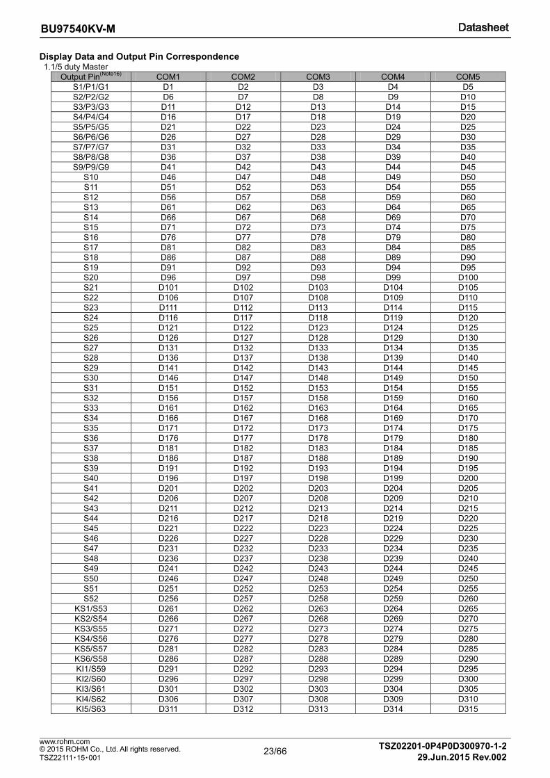
Display Data and Output Pin Correspondence 1.1/5 duty Master
Output Pin(Note16)
COM1 COM2 COM3 COM4 COM5
S1/P1/G1 D1 D2 D3 D4 D5
S2/P2/G2 D6 D7 D8 D9 D10
S3/P3/G3 D11 D12 D13 D14 D15
S4/P4/G4 D16 D17 D18 D19 D20
S5/P5/G5 D21 D22 D23 D24 D25
S6/P6/G6 D26 D27 D28 D29 D30
S7/P7/G7 D31 D32 D33 D34 D35
S8/P8/G8 D36 D37 D38 D39 D40
S9/P9/G9 D41 D42 D43 D44 D45
S10 D46 D47 D48 D49 D50
S11 D51 D52 D53 D54 D55
S12 D56 D57 D58 D59 D60
S13 D61 D62 D63 D64 D65
S14 D66 D67 D68 D69 D70
S15 D71 D72 D73 D74 D75
S16 D76 D77 D78 D79 D80
S17 D81 D82 D83 D84 D85
S18 D86 D87 D88 D89 D90
S19 D91 D92 D93 D94 D95
S20 D96 D97 D98 D99 D100
S21 D101 D102 D103 D104 D105
S22 D106 D107 D108 D109 D110
S23 D111 D112 D113 D114 D115
S24 D116 D117 D118 D119 D120
S25 D121 D122 D123 D124 D125
S26 D126 D127 D128 D129 D130
S27 D131 D132 D133 D134 D135
S28 D136 D137 D138 D139 D140
S29 D141 D142 D143 D144 D145
S30 D146 D147 D148 D149 D150
S31 D151 D152 D153 D154 D155
S32 D156 D157 D158 D159 D160
S33 D161 D162 D163 D164 D165
S34 D166 D167 D168 D169 D170
S35 D171 D172 D173 D174 D175
S36 D176 D177 D178 D179 D180
S37 D181 D182 D183 D184 D185
S38 D186 D187 D188 D189 D190
S39 D191 D192 D193 D194 D195
S40 D196 D197 D198 D199 D200
S41 D201 D202 D203 D204 D205
S42 D206 D207 D208 D209 D210
S43 D211 D212 D213 D214 D215
S44 D216 D217 D218 D219 D220
S45 D221 D222 D223 D224 D225
S46 D226 D227 D228 D229 D230
S47 D231 D232 D233 D234 D235
S48 D236 D237 D238 D239 D240
S49 D241 D242 D243 D244 D245
S50 D246 D247 D248 D249 D250
S51 D251 D252 D253 D254 D255
S52 D256 D257 D258 D259 D260
KS1/S53 D261 D262 D263 D264 D265
KS2/S54 D266 D267 D268 D269 D270
KS3/S55 D271 D272 D273 D274 D275
KS4/S56 D276 D277 D278 D279 D280
KS5/S57 D281 D282 D283 D284 D285
KS6/S58 D286 D287 D288 D289 D290
KI1/S59 D291 D292 D293 D294 D295
KI2/S60 D296 D297 D298 D299 D300
KI3/S61 D301 D302 D303 D304 D305
KI4/S62 D306 D307 D308 D309 D310
KI5/S63 D311 D312 D313 D314 D315
24/66
BU97540KV-M
TSZ02201-0P4P0D300970-1-2 © 2015 ROHM Co., Ltd. All rights reserved. 29.Jun.2015 Rev.002
www.rohm.com
TSZ22111・15・001
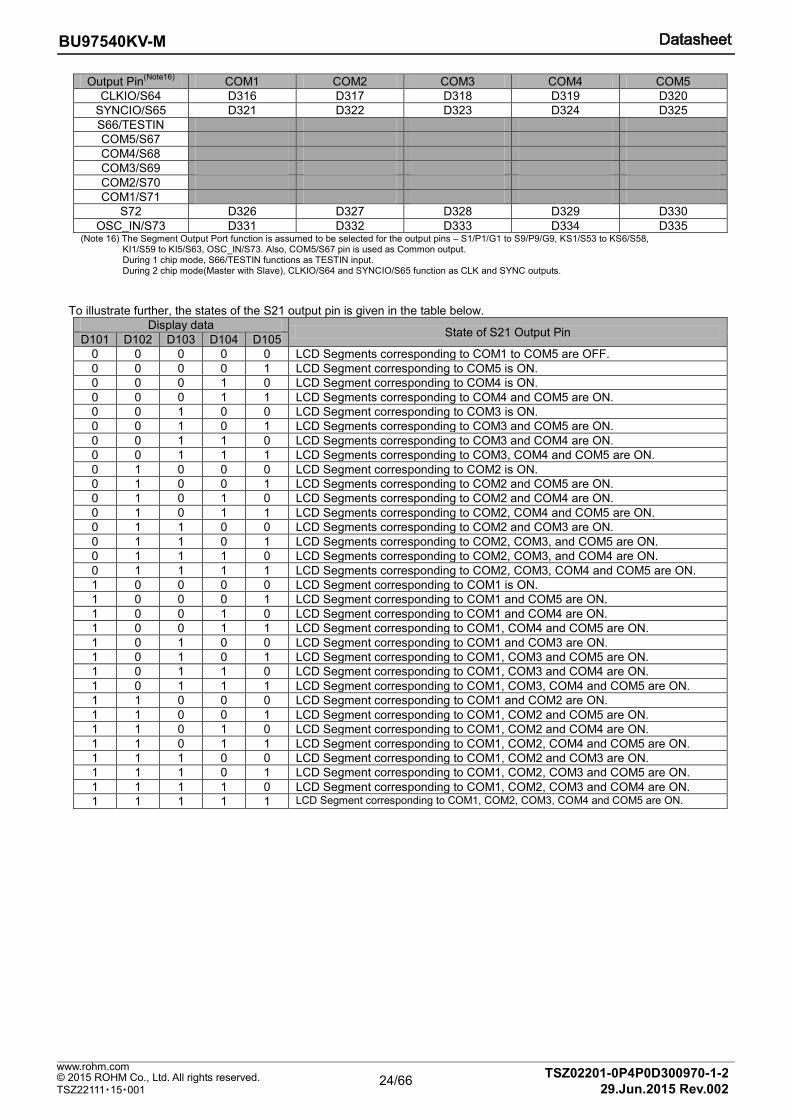
Output Pin(Note16)
COM1 COM2 COM3 COM4 COM5
CLKIO/S64 D316 D317 D318 D319 D320
SYNCIO/S65 D321 D322 D323 D324 D325
S66/TESTIN
COM5/S67
COM4/S68
COM3/S69
COM2/S70
COM1/S71
S72 D326 D327 D328 D329 D330
OSC_IN/S73 D331 D332 D333 D334 D335 (Note 16) The Segment Output Port function is assumed to be selected for the output pins – S1/P1/G1 to S9/P9/G9, KS1/S53 to KS6/S58,
KI1/S59 to KI5/S63, OSC_IN/S73. Also, COM5/S67 pin is used as Common output. During 1 chip mode, S66/TESTIN functions as TESTIN input. During 2 chip mode(Master with Slave), CLKIO/S64 and SYNCIO/S65 function as CLK and SYNC outputs.
To illustrate further, the states of the S21 output pin is given in the table below.
Display data State of S21 Output Pin
D101 D102 D103 D104 D105
0 0 0 0 0 LCD Segments corresponding to COM1 to COM5 are OFF.
0 0 0 0 1 LCD Segment corresponding to COM5 is ON.
0 0 0 1 0 LCD Segment corresponding to COM4 is ON.
0 0 0 1 1 LCD Segments corresponding to COM4 and COM5 are ON.
0 0 1 0 0 LCD Segment corresponding to COM3 is ON.
0 0 1 0 1 LCD Segments corresponding to COM3 and COM5 are ON.
0 0 1 1 0 LCD Segments corresponding to COM3 and COM4 are ON.
0 0 1 1 1 LCD Segments corresponding to COM3, COM4 and COM5 are ON.
0 1 0 0 0 LCD Segment corresponding to COM2 is ON.
0 1 0 0 1 LCD Segments corresponding to COM2 and COM5 are ON.
0 1 0 1 0 LCD Segments corresponding to COM2 and COM4 are ON.
0 1 0 1 1 LCD Segments corresponding to COM2, COM4 and COM5 are ON.
0 1 1 0 0 LCD Segments corresponding to COM2 and COM3 are ON.
0 1 1 0 1 LCD Segments corresponding to COM2, COM3, and COM5 are ON.
0 1 1 1 0 LCD Segments corresponding to COM2, COM3, and COM4 are ON.
0 1 1 1 1 LCD Segments corresponding to COM2, COM3, COM4 and COM5 are ON.
1 0 0 0 0 LCD Segment corresponding to COM1 is ON.
1 0 0 0 1 LCD Segment corresponding to COM1 and COM5 are ON.
1 0 0 1 0 LCD Segment corresponding to COM1 and COM4 are ON.
1 0 0 1 1 LCD Segment corresponding to COM1, COM4 and COM5 are ON.
1 0 1 0 0 LCD Segment corresponding to COM1 and COM3 are ON.
1 0 1 0 1 LCD Segment corresponding to COM1, COM3 and COM5 are ON.
1 0 1 1 0 LCD Segment corresponding to COM1, COM3 and COM4 are ON.
1 0 1 1 1 LCD Segment corresponding to COM1, COM3, COM4 and COM5 are ON.
1 1 0 0 0 LCD Segment corresponding to COM1 and COM2 are ON.
1 1 0 0 1 LCD Segment corresponding to COM1, COM2 and COM5 are ON.
1 1 0 1 0 LCD Segment corresponding to COM1, COM2 and COM4 are ON.
1 1 0 1 1 LCD Segment corresponding to COM1, COM2, COM4 and COM5 are ON.
1 1 1 0 0 LCD Segment corresponding to COM1, COM2 and COM3 are ON.
1 1 1 0 1 LCD Segment corresponding to COM1, COM2, COM3 and COM5 are ON.
1 1 1 1 0 LCD Segment corresponding to COM1, COM2, COM3 and COM4 are ON.
1 1 1 1 1 LCD Segment corresponding to COM1, COM2, COM3, COM4 and COM5 are ON.
25/66
BU97540KV-M
TSZ02201-0P4P0D300970-1-2 © 2015 ROHM Co., Ltd. All rights reserved. 29.Jun.2015 Rev.002
www.rohm.com
TSZ22111・15・001
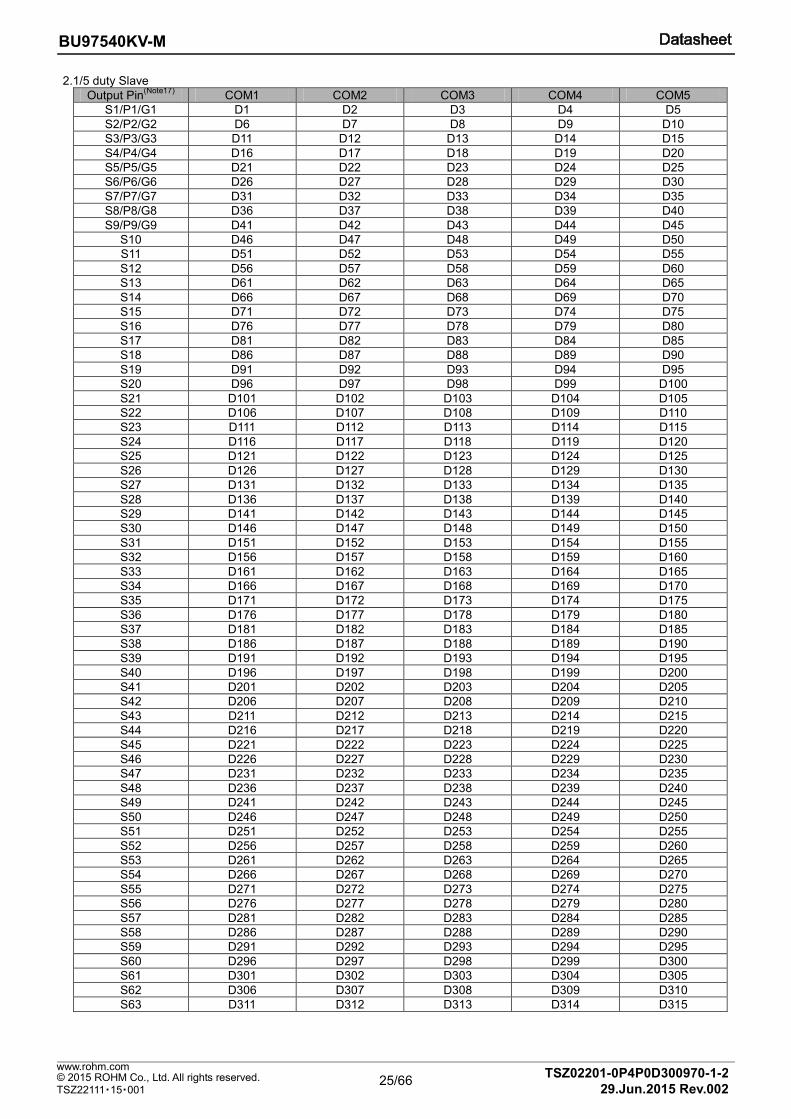
2.1/5 duty Slave
Output Pin(Note17)
COM1 COM2 COM3 COM4 COM5
S1/P1/G1 D1 D2 D3 D4 D5
S2/P2/G2 D6 D7 D8 D9 D10
S3/P3/G3 D11 D12 D13 D14 D15
S4/P4/G4 D16 D17 D18 D19 D20
S5/P5/G5 D21 D22 D23 D24 D25
S6/P6/G6 D26 D27 D28 D29 D30
S7/P7/G7 D31 D32 D33 D34 D35
S8/P8/G8 D36 D37 D38 D39 D40
S9/P9/G9 D41 D42 D43 D44 D45
S10 D46 D47 D48 D49 D50
S11 D51 D52 D53 D54 D55
S12 D56 D57 D58 D59 D60
S13 D61 D62 D63 D64 D65
S14 D66 D67 D68 D69 D70
S15 D71 D72 D73 D74 D75
S16 D76 D77 D78 D79 D80
S17 D81 D82 D83 D84 D85
S18 D86 D87 D88 D89 D90
S19 D91 D92 D93 D94 D95
S20 D96 D97 D98 D99 D100
S21 D101 D102 D103 D104 D105
S22 D106 D107 D108 D109 D110
S23 D111 D112 D113 D114 D115
S24 D116 D117 D118 D119 D120
S25 D121 D122 D123 D124 D125
S26 D126 D127 D128 D129 D130
S27 D131 D132 D133 D134 D135
S28 D136 D137 D138 D139 D140
S29 D141 D142 D143 D144 D145
S30 D146 D147 D148 D149 D150
S31 D151 D152 D153 D154 D155
S32 D156 D157 D158 D159 D160
S33 D161 D162 D163 D164 D165
S34 D166 D167 D168 D169 D170
S35 D171 D172 D173 D174 D175
S36 D176 D177 D178 D179 D180
S37 D181 D182 D183 D184 D185
S38 D186 D187 D188 D189 D190
S39 D191 D192 D193 D194 D195
S40 D196 D197 D198 D199 D200
S41 D201 D202 D203 D204 D205
S42 D206 D207 D208 D209 D210
S43 D211 D212 D213 D214 D215
S44 D216 D217 D218 D219 D220
S45 D221 D222 D223 D224 D225
S46 D226 D227 D228 D229 D230
S47 D231 D232 D233 D234 D235
S48 D236 D237 D238 D239 D240
S49 D241 D242 D243 D244 D245
S50 D246 D247 D248 D249 D250
S51 D251 D252 D253 D254 D255
S52 D256 D257 D258 D259 D260
S53 D261 D262 D263 D264 D265
S54 D266 D267 D268 D269 D270
S55 D271 D272 D273 D274 D275
S56 D276 D277 D278 D279 D280
S57 D281 D282 D283 D284 D285
S58 D286 D287 D288 D289 D290
S59 D291 D292 D293 D294 D295
S60 D296 D297 D298 D299 D300
S61 D301 D302 D303 D304 D305
S62 D306 D307 D308 D309 D310
S63 D311 D312 D313 D314 D315
26/66
BU97540KV-M
TSZ02201-0P4P0D300970-1-2 © 2015 ROHM Co., Ltd. All rights reserved. 29.Jun.2015 Rev.002
www.rohm.com
TSZ22111・15・001
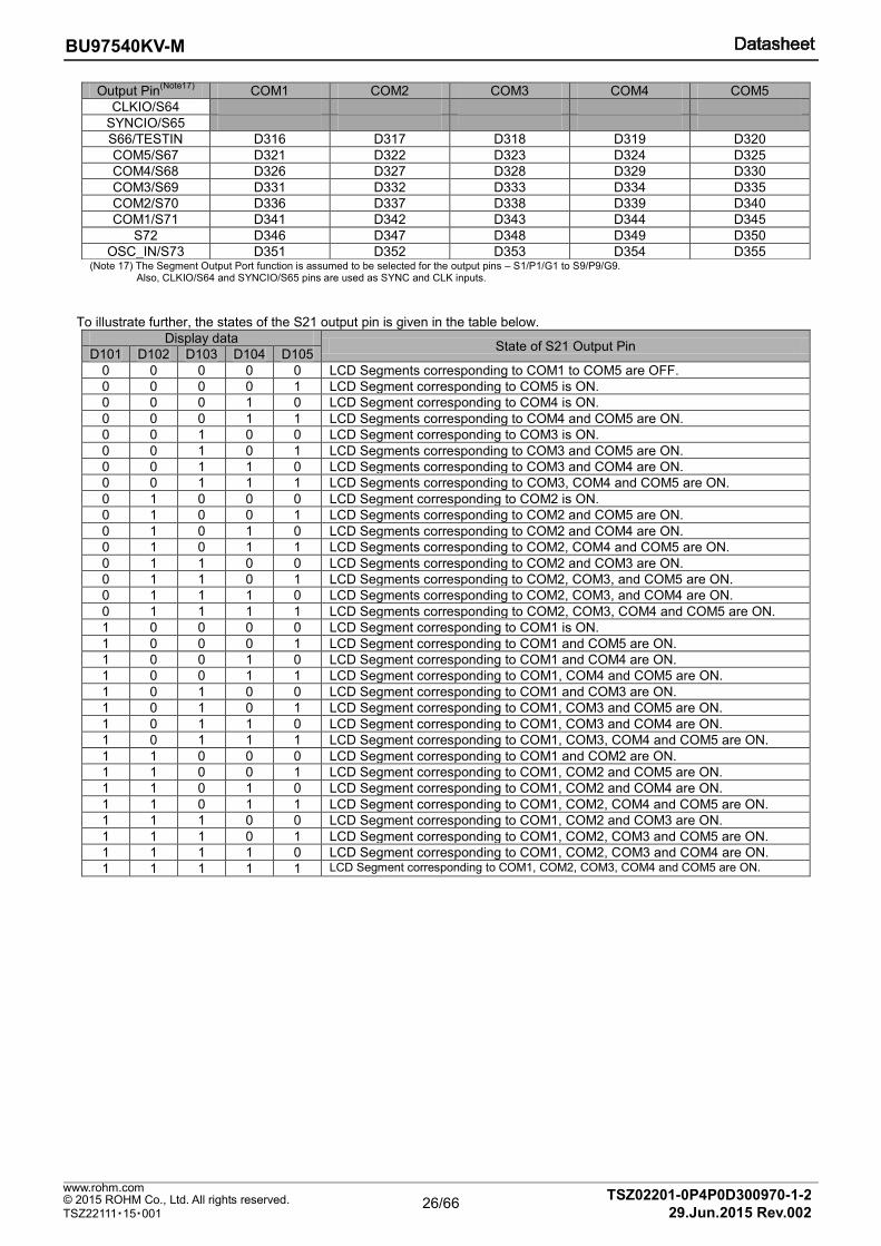
(Note 17) The Segment Output Port function is assumed to be selected for the output pins – S1/P1/G1 to S9/P9/G9. Also, CLKIO/S64 and SYNCIO/S65 pins are used as SYNC and CLK inputs.
To illustrate further, the states of the S21 output pin is given in the table below.
Display data State of S21 Output Pin
D101 D102 D103 D104 D105
0 0 0 0 0 LCD Segments corresponding to COM1 to COM5 are OFF.
0 0 0 0 1 LCD Segment corresponding to COM5 is ON.
0 0 0 1 0 LCD Segment corresponding to COM4 is ON.
0 0 0 1 1 LCD Segments corresponding to COM4 and COM5 are ON.
0 0 1 0 0 LCD Segment corresponding to COM3 is ON.
0 0 1 0 1 LCD Segments corresponding to COM3 and COM5 are ON.
0 0 1 1 0 LCD Segments corresponding to COM3 and COM4 are ON.
0 0 1 1 1 LCD Segments corresponding to COM3, COM4 and COM5 are ON.
0 1 0 0 0 LCD Segment corresponding to COM2 is ON.
0 1 0 0 1 LCD Segments corresponding to COM2 and COM5 are ON.
0 1 0 1 0 LCD Segments corresponding to COM2 and COM4 are ON.
0 1 0 1 1 LCD Segments corresponding to COM2, COM4 and COM5 are ON.
0 1 1 0 0 LCD Segments corresponding to COM2 and COM3 are ON.
0 1 1 0 1 LCD Segments corresponding to COM2, COM3, and COM5 are ON.
0 1 1 1 0 LCD Segments corresponding to COM2, COM3, and COM4 are ON.
0 1 1 1 1 LCD Segments corresponding to COM2, COM3, COM4 and COM5 are ON.
1 0 0 0 0 LCD Segment corresponding to COM1 is ON.
1 0 0 0 1 LCD Segment corresponding to COM1 and COM5 are ON.
1 0 0 1 0 LCD Segment corresponding to COM1 and COM4 are ON.
1 0 0 1 1 LCD Segment corresponding to COM1, COM4 and COM5 are ON.
1 0 1 0 0 LCD Segment corresponding to COM1 and COM3 are ON.
1 0 1 0 1 LCD Segment corresponding to COM1, COM3 and COM5 are ON.
1 0 1 1 0 LCD Segment corresponding to COM1, COM3 and COM4 are ON.
1 0 1 1 1 LCD Segment corresponding to COM1, COM3, COM4 and COM5 are ON.
1 1 0 0 0 LCD Segment corresponding to COM1 and COM2 are ON.
1 1 0 0 1 LCD Segment corresponding to COM1, COM2 and COM5 are ON.
1 1 0 1 0 LCD Segment corresponding to COM1, COM2 and COM4 are ON.
1 1 0 1 1 LCD Segment corresponding to COM1, COM2, COM4 and COM5 are ON.
1 1 1 0 0 LCD Segment corresponding to COM1, COM2 and COM3 are ON.
1 1 1 0 1 LCD Segment corresponding to COM1, COM2, COM3 and COM5 are ON.
1 1 1 1 0 LCD Segment corresponding to COM1, COM2, COM3 and COM4 are ON.
1 1 1 1 1 LCD Segment corresponding to COM1, COM2, COM3, COM4 and COM5 are ON.
Output Pin(Note17)
COM1 COM2 COM3 COM4 COM5
CLKIO/S64
SYNCIO/S65
S66/TESTIN D316 D317 D318 D319 D320
COM5/S67 D321 D322 D323 D324 D325
COM4/S68 D326 D327 D328 D329 D330
COM3/S69 D331 D332 D333 D334 D335
COM2/S70 D336 D337 D338 D339 D340
COM1/S71 D341 D342 D343 D344 D345
S72 D346 D347 D348 D349 D350
OSC_IN/S73 D351 D352 D353 D354 D355
27/66
BU97540KV-M
TSZ02201-0P4P0D300970-1-2 © 2015 ROHM Co., Ltd. All rights reserved. 29.Jun.2015 Rev.002
www.rohm.com
TSZ22111・15・001
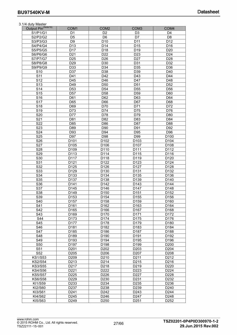
3.1/4 duty Master
Output Pin(Note18)
COM1 COM2 COM3 COM4
S1/P1/G1 D1 D2 D3 D4
S2/P2/G2 D5 D6 D7 D8
S3/P3/G3 D9 D10 D11 D12
S4/P4/G4 D13 D14 D15 D16
S5/P5/G5 D17 D18 D19 D20
S6/P6/G6 D21 D22 D23 D24
S7/P7/G7 D25 D26 D27 D28
S8/P8/G8 D29 D30 D31 D32
S9/P9/G9 D33 D34 D35 D36
S10 D37 D38 D39 D40
S11 D41 D42 D43 D44
S12 D45 D46 D47 D48
S13 D49 D50 D51 D52
S14 D53 D54 D55 D56
S15 D57 D58 D59 D60
S16 D61 D62 D63 D64
S17 D65 D66 D67 D68
S18 D69 D70 D71 D72
S19 D73 D74 D75 D76
S20 D77 D78 D79 D80
S21 D81 D82 D83 D84
S22 D85 D86 D87 D88
S23 D89 D90 D91 D92
S24 D93 D94 D95 D96
S25 D97 D98 D99 D100
S26 D101 D102 D103 D104
S27 D105 D106 D107 D108
S28 D109 D110 D111 D112
S29 D113 D114 D115 D116
S30 D117 D118 D119 D120
S31 D121 D122 D123 D124
S32 D125 D126 D127 D128
S33 D129 D130 D131 D132
S34 D133 D134 D135 D136
S35 D137 D138 D139 D140
S36 D141 D142 D143 D144
S37 D145 D146 D147 D148
S38 D149 D150 D151 D152
S39 D153 D154 D155 D156
S40 D157 D158 D159 D160
S41 D161 D162 D163 D164
S42 D165 D166 D167 D168
S43 D169 D170 D171 D172
S44 D173 D174 D175 D176
S45 D177 D178 D179 D180
S46 D181 D182 D183 D184
S47 D185 D186 D187 D188
S48 D189 D190 D191 D192
S49 D193 D194 D195 D196
S50 D197 D198 D199 D200
S51 D201 D202 D203 D204
S52 D205 D206 D207 D208
KS1/S53 D209 D210 D211 D212
KS2/S54 D213 D214 D215 D216
KS3/S55 D217 D218 D219 D220
KS4/S56 D221 D222 D223 D224
KS5/S57 D225 D226 D227 D228
KS6/S58 D229 D230 D231 D232
KI1/S59 D233 D234 D235 D236
KI2/S60 D237 D238 D239 D240
KI3/S61 D241 D242 D243 D244
KI4/S62 D245 D246 D247 D248
KI5/S63 D249 D250 D251 D252
28/66
BU97540KV-M
TSZ02201-0P4P0D300970-1-2 © 2015 ROHM Co., Ltd. All rights reserved. 29.Jun.2015 Rev.002
www.rohm.com
TSZ22111・15・001
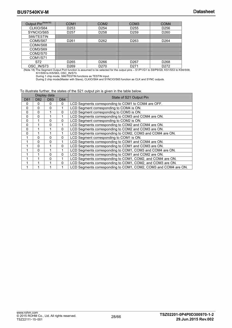
Output Pin(Note18)
COM1 COM2 COM3 COM4
CLKIO/S64 D253 D254 D255 D256
SYNCIO/S65 D257 D258 D259 D260
S66/TESTIN
COM5/S67 D261 D262 D263 D264
COM4/S68
COM3/S69
COM2/S70
COM1/S71
S72 D265 D266 D267 D268
OSC_IN/S73 D269 D270 D271 D272 (Note 18) The Segment Output Port function is assumed to be selected for the output pins – S1/P1/G1 to S9/P9/G9, KS1/S53 to KS6/S58,
KI1/S59 to KI5/S63, OSC_IN/S73. During 1 chip mode, S66/TESTIN functions as TESTIN input. During 2 chip mode(Master with Slave), CLKIO/S64 and SYNCIO/S65 function as CLK and SYNC outputs.
To illustrate further, the states of the S21 output pin is given in the table below.
Display data State of S21 Output Pin
D81 D82 D83 D84
0 0 0 0 LCD Segments corresponding to COM1 to COM4 are OFF.
0 0 0 1 LCD Segment corresponding to COM4 is ON.
0 0 1 0 LCD Segment corresponding to COM3 is ON.
0 0 1 1 LCD Segments corresponding to COM3 and COM4 are ON.
0 1 0 0 LCD Segment corresponding to COM2 is ON.
0 1 0 1 LCD Segments corresponding to COM2 and COM4 are ON.
0 1 1 0 LCD Segments corresponding to COM2 and COM3 are ON.
0 1 1 1 LCD Segments corresponding to COM2, COM3 and COM4 are ON.
1 0 0 0 LCD Segment corresponding to COM1 is ON.
1 0 0 1 LCD Segments corresponding to COM1 and COM4 are ON.
1 0 1 0 LCD Segments corresponding to COM1 and COM3 are ON.
1 0 1 1 LCD Segments corresponding to COM1, COM3 and COM4 are ON.
1 1 0 0 LCD Segments corresponding to COM1 and COM2 are ON.
1 1 0 1 LCD Segments corresponding to COM1, COM2, and COM4 are ON.
1 1 1 0 LCD Segments corresponding to COM1, COM2, and COM3 are ON.
1 1 1 1 LCD Segments corresponding to COM1, COM2, COM3 and COM4 are ON.
29/66
BU97540KV-M
TSZ02201-0P4P0D300970-1-2 © 2015 ROHM Co., Ltd. All rights reserved. 29.Jun.2015 Rev.002
www.rohm.com
TSZ22111・15・001
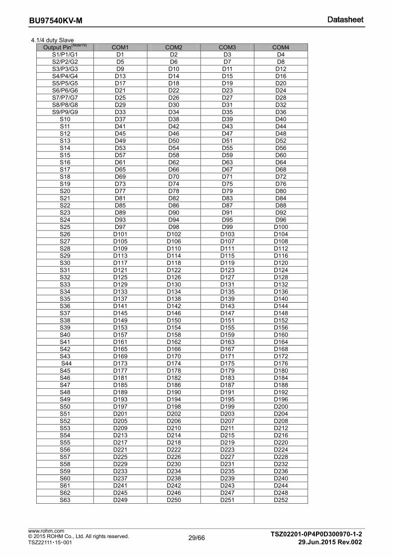
4.1/4 duty Slave
Output Pin(Note19)
COM1 COM2 COM3 COM4
S1/P1/G1 D1 D2 D3 D4
S2/P2/G2 D5 D6 D7 D8
S3/P3/G3 D9 D10 D11 D12
S4/P4/G4 D13 D14 D15 D16
S5/P5/G5 D17 D18 D19 D20
S6/P6/G6 D21 D22 D23 D24
S7/P7/G7 D25 D26 D27 D28
S8/P8/G8 D29 D30 D31 D32
S9/P9/G9 D33 D34 D35 D36
S10 D37 D38 D39 D40
S11 D41 D42 D43 D44
S12 D45 D46 D47 D48
S13 D49 D50 D51 D52
S14 D53 D54 D55 D56
S15 D57 D58 D59 D60
S16 D61 D62 D63 D64
S17 D65 D66 D67 D68
S18 D69 D70 D71 D72
S19 D73 D74 D75 D76
S20 D77 D78 D79 D80
S21 D81 D82 D83 D84
S22 D85 D86 D87 D88
S23 D89 D90 D91 D92
S24 D93 D94 D95 D96
S25 D97 D98 D99 D100
S26 D101 D102 D103 D104
S27 D105 D106 D107 D108
S28 D109 D110 D111 D112
S29 D113 D114 D115 D116
S30 D117 D118 D119 D120
S31 D121 D122 D123 D124
S32 D125 D126 D127 D128
S33 D129 D130 D131 D132
S34 D133 D134 D135 D136
S35 D137 D138 D139 D140
S36 D141 D142 D143 D144
S37 D145 D146 D147 D148
S38 D149 D150 D151 D152
S39 D153 D154 D155 D156
S40 D157 D158 D159 D160
S41 D161 D162 D163 D164
S42 D165 D166 D167 D168
S43 D169 D170 D171 D172
S44 D173 D174 D175 D176
S45 D177 D178 D179 D180
S46 D181 D182 D183 D184
S47 D185 D186 D187 D188
S48 D189 D190 D191 D192
S49 D193 D194 D195 D196
S50 D197 D198 D199 D200
S51 D201 D202 D203 D204
S52 D205 D206 D207 D208
S53 D209 D210 D211 D212
S54 D213 D214 D215 D216
S55 D217 D218 D219 D220
S56 D221 D222 D223 D224
S57 D225 D226 D227 D228
S58 D229 D230 D231 D232
S59 D233 D234 D235 D236
S60 D237 D238 D239 D240
S61 D241 D242 D243 D244
S62 D245 D246 D247 D248
S63 D249 D250 D251 D252
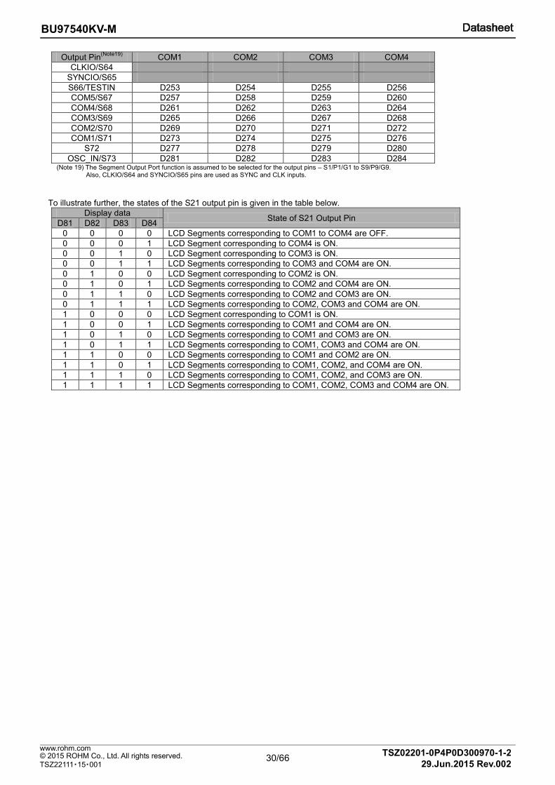
30/66
BU97540KV-M
TSZ02201-0P4P0D300970-1-2 © 2015 ROHM Co., Ltd. All rights reserved. 29.Jun.2015 Rev.002
www.rohm.com
TSZ22111・15・001
Output Pin(Note19)
COM1 COM2 COM3 COM4
CLKIO/S64
SYNCIO/S65
S66/TESTIN D253 D254 D255 D256
COM5/S67 D257 D258 D259 D260
COM4/S68 D261 D262 D263 D264
COM3/S69 D265 D266 D267 D268
COM2/S70 D269 D270 D271 D272
COM1/S71 D273 D274 D275 D276
S72 D277 D278 D279 D280
OSC_IN/S73 D281 D282 D283 D284 (Note 19) The Segment Output Port function is assumed to be selected for the output pins – S1/P1/G1 to S9/P9/G9.
Also, CLKIO/S64 and SYNCIO/S65 pins are used as SYNC and CLK inputs.
To illustrate further, the states of the S21 output pin is given in the table below.
Display data State of S21 Output Pin
D81 D82 D83 D84
0 0 0 0 LCD Segments corresponding to COM1 to COM4 are OFF.
0 0 0 1 LCD Segment corresponding to COM4 is ON.
0 0 1 0 LCD Segment corresponding to COM3 is ON.
0 0 1 1 LCD Segments corresponding to COM3 and COM4 are ON.
0 1 0 0 LCD Segment corresponding to COM2 is ON.
0 1 0 1 LCD Segments corresponding to COM2 and COM4 are ON.
0 1 1 0 LCD Segments corresponding to COM2 and COM3 are ON.
0 1 1 1 LCD Segments corresponding to COM2, COM3 and COM4 are ON.
1 0 0 0 LCD Segment corresponding to COM1 is ON.
1 0 0 1 LCD Segments corresponding to COM1 and COM4 are ON.
1 0 1 0 LCD Segments corresponding to COM1 and COM3 are ON.
1 0 1 1 LCD Segments corresponding to COM1, COM3 and COM4 are ON.
1 1 0 0 LCD Segments corresponding to COM1 and COM2 are ON.
1 1 0 1 LCD Segments corresponding to COM1, COM2, and COM4 are ON.
1 1 1 0 LCD Segments corresponding to COM1, COM2, and COM3 are ON.
1 1 1 1 LCD Segments corresponding to COM1, COM2, COM3 and COM4 are ON.
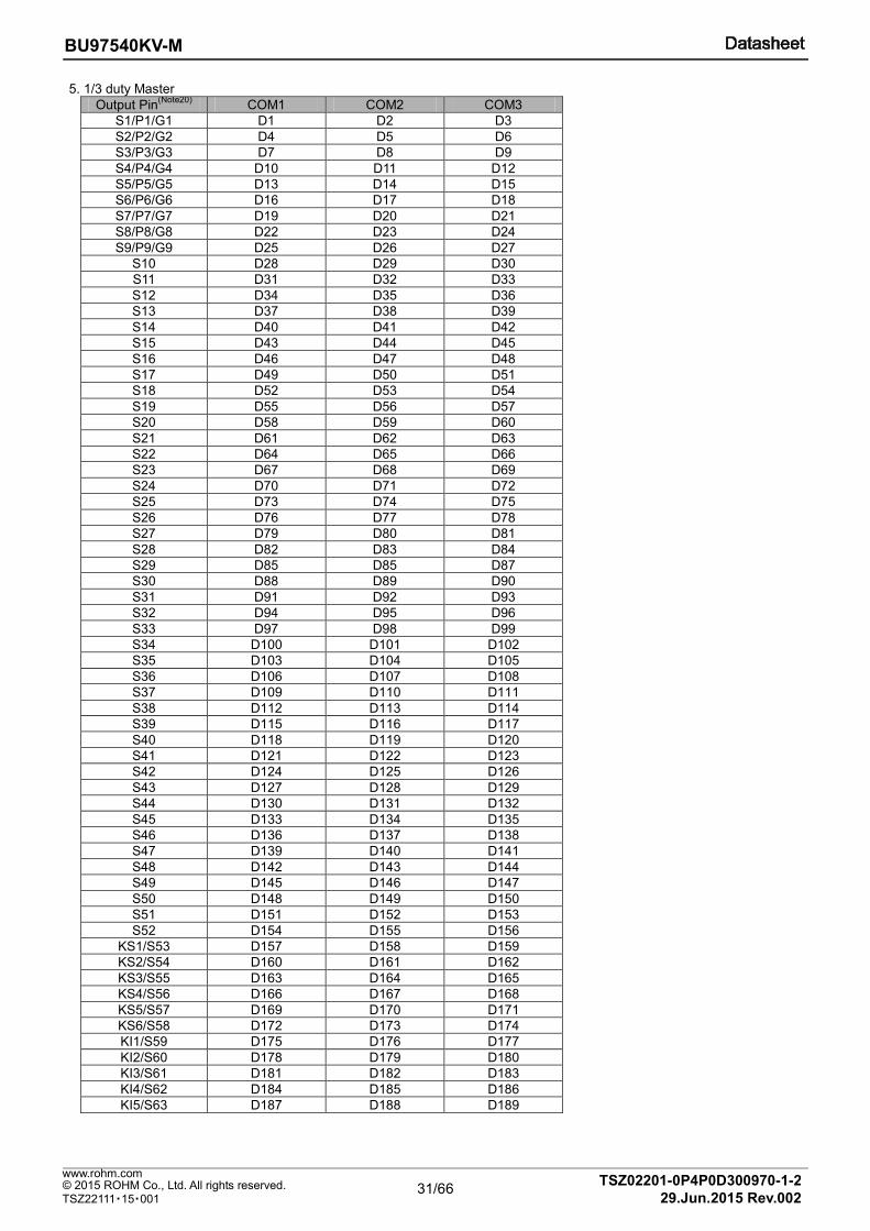
31/66
BU97540KV-M
TSZ02201-0P4P0D300970-1-2 © 2015 ROHM Co., Ltd. All rights reserved. 29.Jun.2015 Rev.002
www.rohm.com
TSZ22111・15・001
5. 1/3 duty Master
Output Pin(Note20)
COM1 COM2 COM3
S1/P1/G1 D1 D2 D3
S2/P2/G2 D4 D5 D6
S3/P3/G3 D7 D8 D9
S4/P4/G4 D10 D11 D12
S5/P5/G5 D13 D14 D15
S6/P6/G6 D16 D17 D18
S7/P7/G7 D19 D20 D21
S8/P8/G8 D22 D23 D24
S9/P9/G9 D25 D26 D27
S10 D28 D29 D30
S11 D31 D32 D33
S12 D34 D35 D36
S13 D37 D38 D39
S14 D40 D41 D42
S15 D43 D44 D45
S16 D46 D47 D48
S17 D49 D50 D51
S18 D52 D53 D54
S19 D55 D56 D57
S20 D58 D59 D60
S21 D61 D62 D63
S22 D64 D65 D66
S23 D67 D68 D69
S24 D70 D71 D72
S25 D73 D74 D75
S26 D76 D77 D78
S27 D79 D80 D81
S28 D82 D83 D84
S29 D85 D85 D87
S30 D88 D89 D90
S31 D91 D92 D93
S32 D94 D95 D96
S33 D97 D98 D99
S34 D100 D101 D102
S35 D103 D104 D105
S36 D106 D107 D108
S37 D109 D110 D111
S38 D112 D113 D114
S39 D115 D116 D117
S40 D118 D119 D120
S41 D121 D122 D123
S42 D124 D125 D126
S43 D127 D128 D129
S44 D130 D131 D132
S45 D133 D134 D135
S46 D136 D137 D138
S47 D139 D140 D141
S48 D142 D143 D144
S49 D145 D146 D147
S50 D148 D149 D150
S51 D151 D152 D153
S52 D154 D155 D156
KS1/S53 D157 D158 D159
KS2/S54 D160 D161 D162
KS3/S55 D163 D164 D165
KS4/S56 D166 D167 D168
KS5/S57 D169 D170 D171
KS6/S58 D172 D173 D174
KI1/S59 D175 D176 D177
KI2/S60 D178 D179 D180
KI3/S61 D181 D182 D183
KI4/S62 D184 D185 D186
KI5/S63 D187 D188 D189
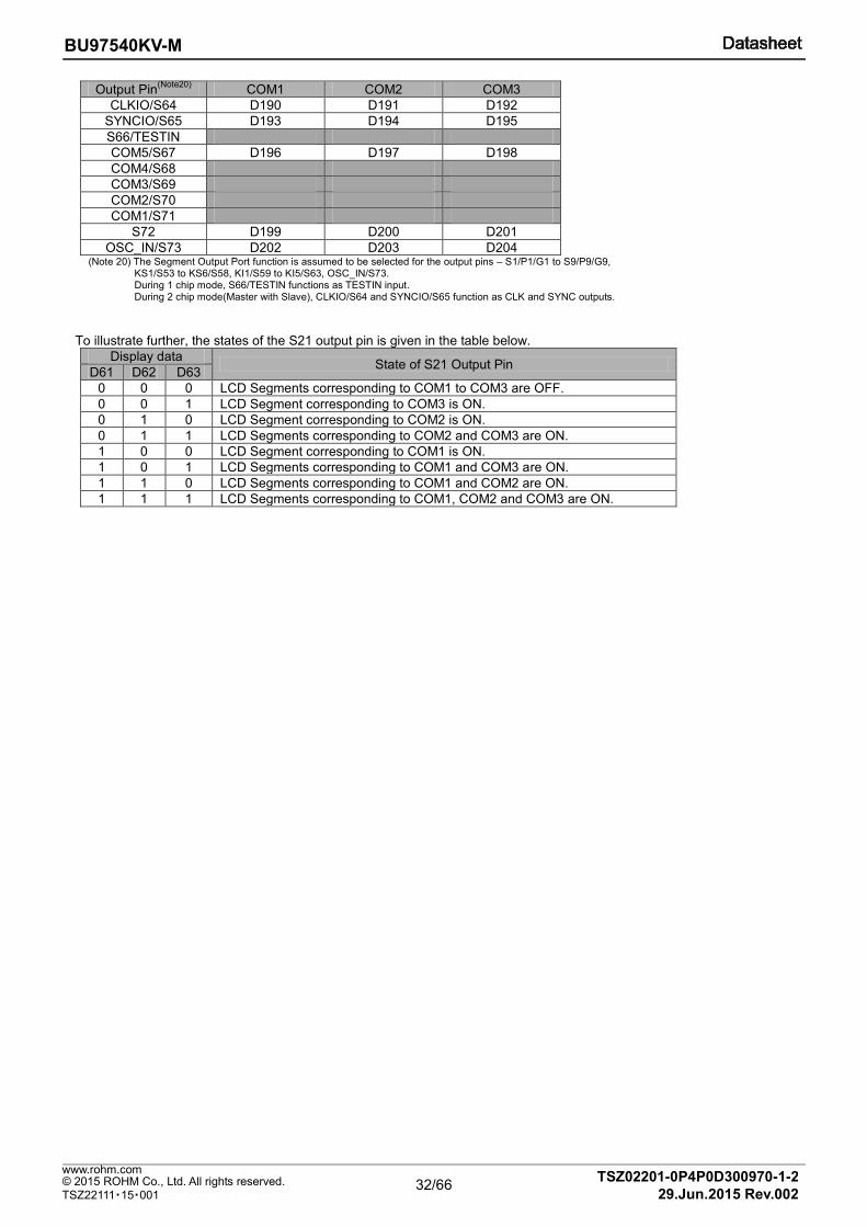
32/66
BU97540KV-M
TSZ02201-0P4P0D300970-1-2 © 2015 ROHM Co., Ltd. All rights reserved. 29.Jun.2015 Rev.002
www.rohm.com
TSZ22111・15・001
Output Pin(Note20)
COM1 COM2 COM3
CLKIO/S64 D190 D191 D192
SYNCIO/S65 D193 D194 D195
S66/TESTIN
COM5/S67 D196 D197 D198
COM4/S68
COM3/S69
COM2/S70
COM1/S71
S72 D199 D200 D201
OSC_IN/S73 D202 D203 D204 (Note 20) The Segment Output Port function is assumed to be selected for the output pins – S1/P1/G1 to S9/P9/G9,
KS1/S53 to KS6/S58, KI1/S59 to KI5/S63, OSC_IN/S73. During 1 chip mode, S66/TESTIN functions as TESTIN input. During 2 chip mode(Master with Slave), CLKIO/S64 and SYNCIO/S65 function as CLK and SYNC outputs.
To illustrate further, the states of the S21 output pin is given in the table below.
Display data State of S21 Output Pin
D61 D62 D63
0 0 0 LCD Segments corresponding to COM1 to COM3 are OFF.
0 0 1 LCD Segment corresponding to COM3 is ON.
0 1 0 LCD Segment corresponding to COM2 is ON.
0 1 1 LCD Segments corresponding to COM2 and COM3 are ON.
1 0 0 LCD Segment corresponding to COM1 is ON.
1 0 1 LCD Segments corresponding to COM1 and COM3 are ON.
1 1 0 LCD Segments corresponding to COM1 and COM2 are ON.
1 1 1 LCD Segments corresponding to COM1, COM2 and COM3 are ON.
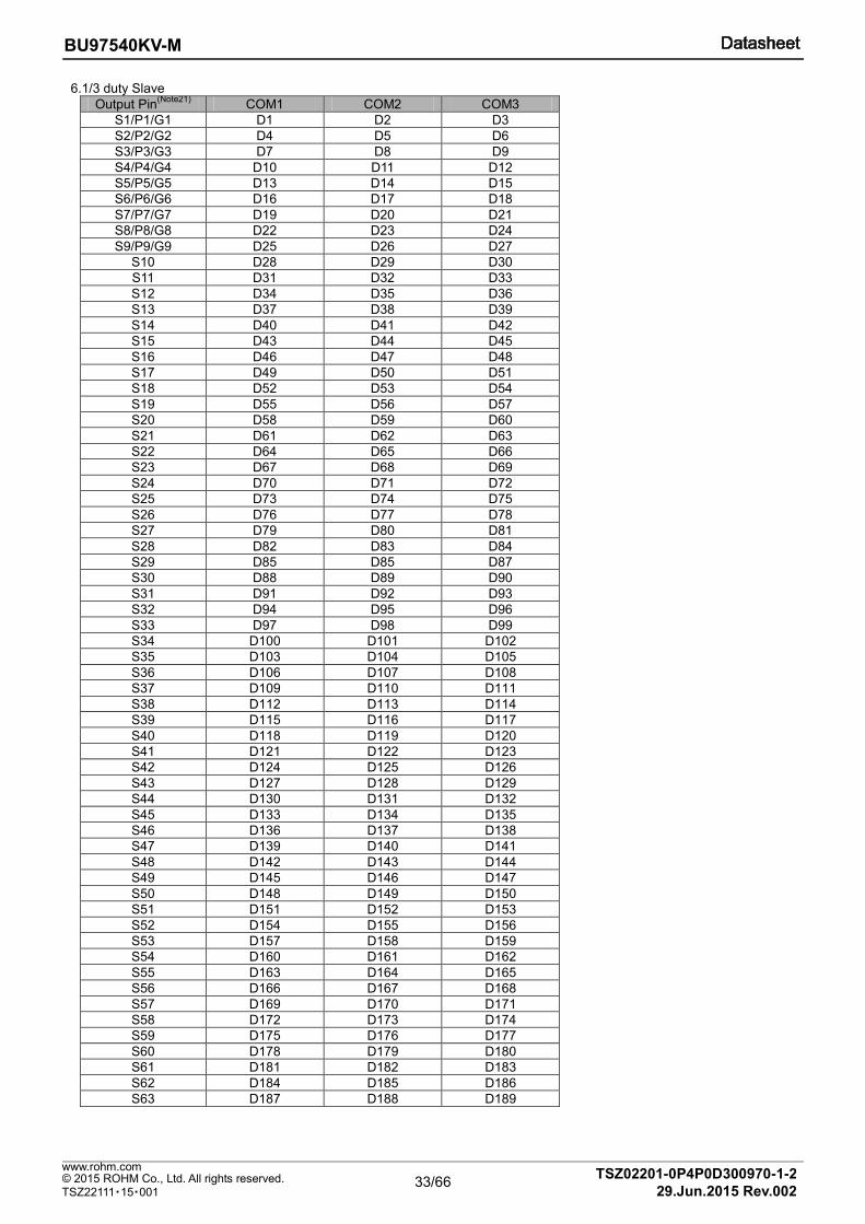
33/66
BU97540KV-M
TSZ02201-0P4P0D300970-1-2 © 2015 ROHM Co., Ltd. All rights reserved. 29.Jun.2015 Rev.002
www.rohm.com
TSZ22111・15・001
6.1/3 duty Slave
Output Pin(Note21)
COM1 COM2 COM3
S1/P1/G1 D1 D2 D3
S2/P2/G2 D4 D5 D6
S3/P3/G3 D7 D8 D9
S4/P4/G4 D10 D11 D12
S5/P5/G5 D13 D14 D15
S6/P6/G6 D16 D17 D18
S7/P7/G7 D19 D20 D21
S8/P8/G8 D22 D23 D24
S9/P9/G9 D25 D26 D27
S10 D28 D29 D30
S11 D31 D32 D33
S12 D34 D35 D36
S13 D37 D38 D39
S14 D40 D41 D42
S15 D43 D44 D45
S16 D46 D47 D48
S17 D49 D50 D51
S18 D52 D53 D54
S19 D55 D56 D57
S20 D58 D59 D60
S21 D61 D62 D63
S22 D64 D65 D66
S23 D67 D68 D69
S24 D70 D71 D72
S25 D73 D74 D75
S26 D76 D77 D78
S27 D79 D80 D81
S28 D82 D83 D84
S29 D85 D85 D87
S30 D88 D89 D90
S31 D91 D92 D93
S32 D94 D95 D96
S33 D97 D98 D99
S34 D100 D101 D102
S35 D103 D104 D105
S36 D106 D107 D108
S37 D109 D110 D111
S38 D112 D113 D114
S39 D115 D116 D117
S40 D118 D119 D120
S41 D121 D122 D123
S42 D124 D125 D126
S43 D127 D128 D129
S44 D130 D131 D132
S45 D133 D134 D135
S46 D136 D137 D138
S47 D139 D140 D141
S48 D142 D143 D144
S49 D145 D146 D147
S50 D148 D149 D150
S51 D151 D152 D153
S52 D154 D155 D156
S53 D157 D158 D159
S54 D160 D161 D162
S55 D163 D164 D165
S56 D166 D167 D168
S57 D169 D170 D171
S58 D172 D173 D174
S59 D175 D176 D177
S60 D178 D179 D180
S61 D181 D182 D183
S62 D184 D185 D186
S63 D187 D188 D189
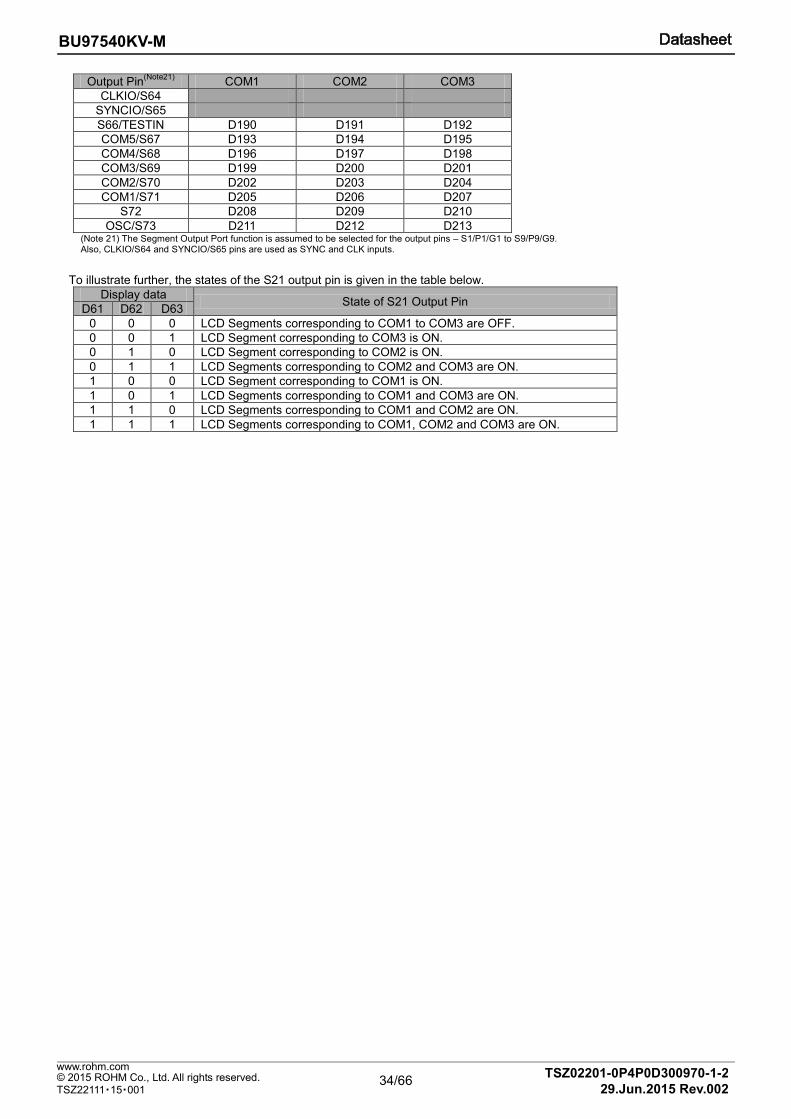
34/66
BU97540KV-M
TSZ02201-0P4P0D300970-1-2 © 2015 ROHM Co., Ltd. All rights reserved. 29.Jun.2015 Rev.002
www.rohm.com
TSZ22111・15・001
Output Pin(Note21)
COM1 COM2 COM3
CLKIO/S64
SYNCIO/S65
S66/TESTIN D190 D191 D192
COM5/S67 D193 D194 D195
COM4/S68 D196 D197 D198
COM3/S69 D199 D200 D201
COM2/S70 D202 D203 D204
COM1/S71 D205 D206 D207
S72 D208 D209 D210
OSC/S73 D211 D212 D213 (Note 21) The Segment Output Port function is assumed to be selected for the output pins – S1/P1/G1 to S9/P9/G9. Also, CLKIO/S64 and SYNCIO/S65 pins are used as SYNC and CLK inputs.
To illustrate further, the states of the S21 output pin is given in the table below.
Display data State of S21 Output Pin
D61 D62 D63
0 0 0 LCD Segments corresponding to COM1 to COM3 are OFF.
0 0 1 LCD Segment corresponding to COM3 is ON.
0 1 0 LCD Segment corresponding to COM2 is ON.
0 1 1 LCD Segments corresponding to COM2 and COM3 are ON.
1 0 0 LCD Segment corresponding to COM1 is ON.
1 0 1 LCD Segments corresponding to COM1 and COM3 are ON.
1 1 0 LCD Segments corresponding to COM1 and COM2 are ON.
1 1 1 LCD Segments corresponding to COM1, COM2 and COM3 are ON.
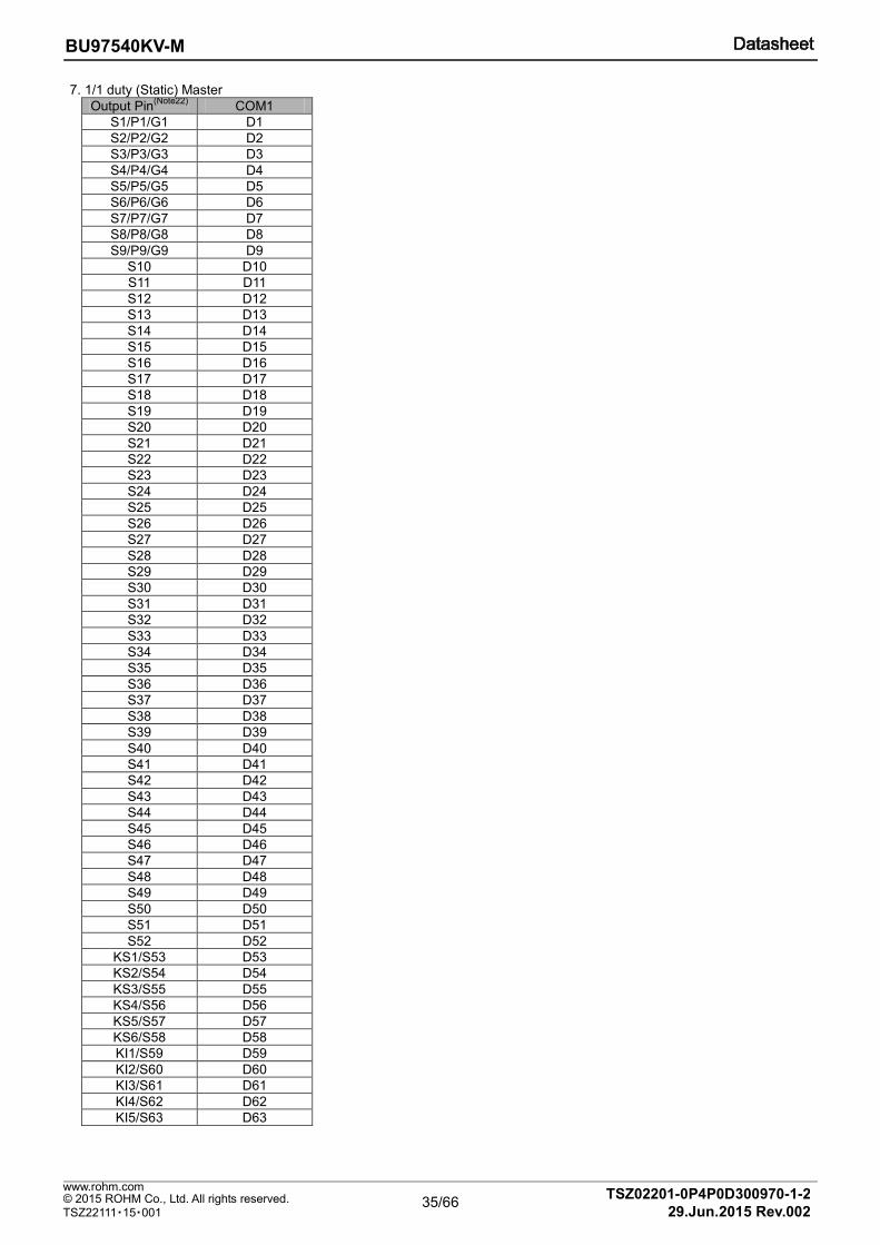
35/66
BU97540KV-M
TSZ02201-0P4P0D300970-1-2 © 2015 ROHM Co., Ltd. All rights reserved. 29.Jun.2015 Rev.002
www.rohm.com
TSZ22111・15・001
7. 1/1 duty (Static) Master
Output Pin(Note22)
COM1
S1/P1/G1 D1
S2/P2/G2 D2
S3/P3/G3 D3
S4/P4/G4 D4
S5/P5/G5 D5
S6/P6/G6 D6
S7/P7/G7 D7
S8/P8/G8 D8
S9/P9/G9 D9
S10 D10
S11 D11
S12 D12
S13 D13
S14 D14
S15 D15
S16 D16
S17 D17
S18 D18
S19 D19
S20 D20
S21 D21
S22 D22
S23 D23
S24 D24
S25 D25
S26 D26
S27 D27
S28 D28
S29 D29
S30 D30
S31 D31
S32 D32
S33 D33
S34 D34
S35 D35
S36 D36
S37 D37
S38 D38
S39 D39
S40 D40
S41 D41
S42 D42
S43 D43
S44 D44
S45 D45
S46 D46
S47 D47
S48 D48
S49 D49
S50 D50
S51 D51
S52 D52
KS1/S53 D53
KS2/S54 D54
KS3/S55 D55
KS4/S56 D56
KS5/S57 D57
KS6/S58 D58
KI1/S59 D59
KI2/S60 D60
KI3/S61 D61
KI4/S62 D62
KI5/S63 D63
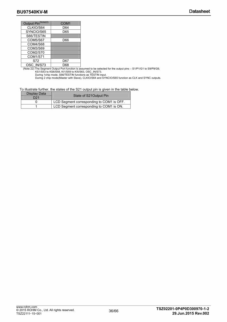
36/66
BU97540KV-M
TSZ02201-0P4P0D300970-1-2 © 2015 ROHM Co., Ltd. All rights reserved. 29.Jun.2015 Rev.002
www.rohm.com
TSZ22111・15・001
Output Pin(Note22)
COM1
CLKIO/S64 D64
SYNCIO/S65 D65
S66/TESTIN
COM5/S67 D66
COM4/S68
COM3/S69
COM2/S70
COM1/S71
S72 D67
OSC_IN/S73 D68 (Note 22) The Segment Output Port function is assumed to be selected for the output pins – S1/P1/G1 to S9/P9/G9,
KS1/S53 to KS6/S58, KI1/S59 to KI5/S63, OSC_IN/S73. During 1chip mode, S66/TESTIN functions as TESTIN input. During 2 chip mode(Master with Slave), CLKIO/S64 and SYNCIO/S65 function as CLK and SYNC outputs.
To illustrate further, the states of the S21 output pin is given in the table below.
Display Data State of S21Output Pin
D21
0 LCD Segment corresponding to COM1 is OFF.
1 LCD Segment corresponding to COM1 is ON.
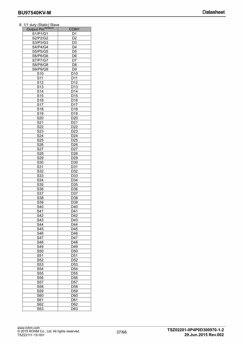
37/66
BU97540KV-M
TSZ02201-0P4P0D300970-1-2 © 2015 ROHM Co., Ltd. All rights reserved. 29.Jun.2015 Rev.002
www.rohm.com
TSZ22111・15・001
8. 1/1 duty (Static) Slave Output Pin
(Note23) COM1
S1/P1/G1 D1
S2/P2/G2 D2
S3/P3/G3 D3
S4/P4/G4 D4
S5/P5/G5 D5
S6/P6/G6 D6
S7/P7/G7 D7
S8/P8/G8 D8
S9/P9/G9 D9
S10 D10
S11 D11
S12 D12
S13 D13
S14 D14
S15 D15
S16 D16
S17 D17
S18 D18
S19 D19
S20 D20
S21 D21
S22 D22
S23 D23
S24 D24
S25 D25
S26 D26
S27 D27
S28 D28
S29 D29
S30 D30
S31 D31
S32 D32
S33 D33
S34 D34
S35 D35
S36 D36
S37 D37
S38 D38
S39 D39
S40 D40
S41 D41
S42 D42
S43 D43
S44 D44
S45 D45
S46 D46
S47 D47
S48 D48
S49 D49
S50 D50
S51 D51
S52 D52
S53 D53
S54 D54
S55 D55
S56 D56
S57 D57
S58 D58
S59 D59
S60 D60
S61 D61
S62 D62
S63 D63
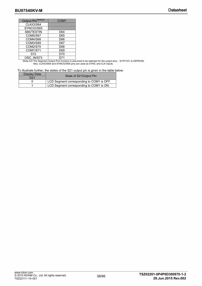
38/66
BU97540KV-M
TSZ02201-0P4P0D300970-1-2 © 2015 ROHM Co., Ltd. All rights reserved. 29.Jun.2015 Rev.002
www.rohm.com
TSZ22111・15・001
Output Pin(Note23)
COM1
CLKIO/S64
SYNCIO/S65
S66/TESTIN D64
COM5/S67 D65
COM4/S68 D66
COM3/S69 D67
COM2/S70 D68
COM1/S71 D69
S72 D70
OSC_IN/S73 D71 (Note 23) The Segment Output Port function is assumed to be selected for the output pins – S1/P1/G1 to S9/P9/G9.
Also, CLKIO/S64 and SYNCIO/S65 pins are used as SYNC and CLK inputs.
To illustrate further, the states of the S21 output pin is given in the table below.
Display Data State of S21Output Pin
D21
0 LCD Segment corresponding to COM1 is OFF.
1 LCD Segment corresponding to COM1 is ON.
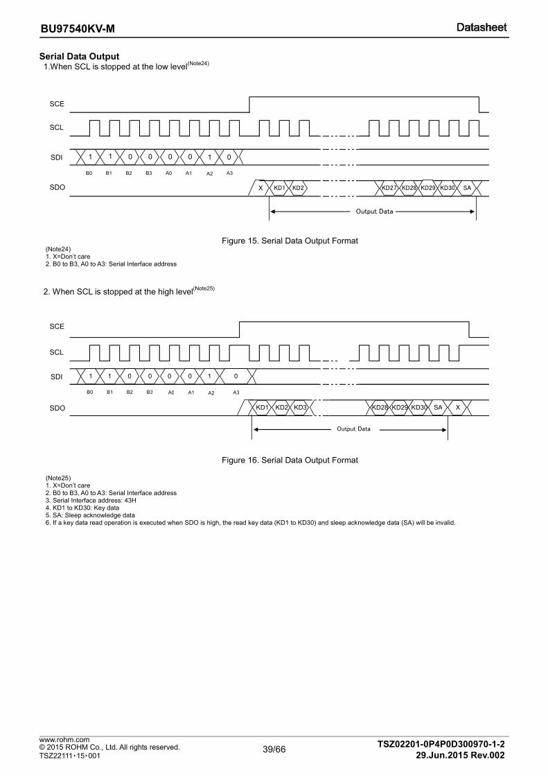
39/66
BU97540KV-M
TSZ02201-0P4P0D300970-1-2 © 2015 ROHM Co., Ltd. All rights reserved. 29.Jun.2015 Rev.002
www.rohm.com
TSZ22111・15・001
Serial Data Output 1.When SCL is stopped at the low level
(Note24)
Output Data
KD28KD27
B0
KD2KD1X KD30KD29 SA
B1 B2 B3 A0 A1 A2 A3
1 0 0 0 0 11 0
SCE
SCL
SDI
SDO
Figure 15. Serial Data Output Format
(Note24) 1. X=Don’t care 2. B0 to B3, A0 to A3: Serial Interface address
2. When SCL is stopped at the high level
(Note25)
Output Data
KD29KD28
1 0 0 0 0 1 01
KD2KD1 SAKD30 XKD3
B0 B1 B2 B3 A0 A1 A2 A3
SCE
SCL
SDI
SDO
Figure 16. Serial Data Output Format
(Note25) 1. X=Don’t care 2. B0 to B3, A0 to A3: Serial Interface address 3. Serial Interface address: 43H 4. KD1 to KD30: Key data 5. SA: Sleep acknowledge data 6. If a key data read operation is executed when SDO is high, the read key data (KD1 to KD30) and sleep acknowledge data (SA) will be invalid.
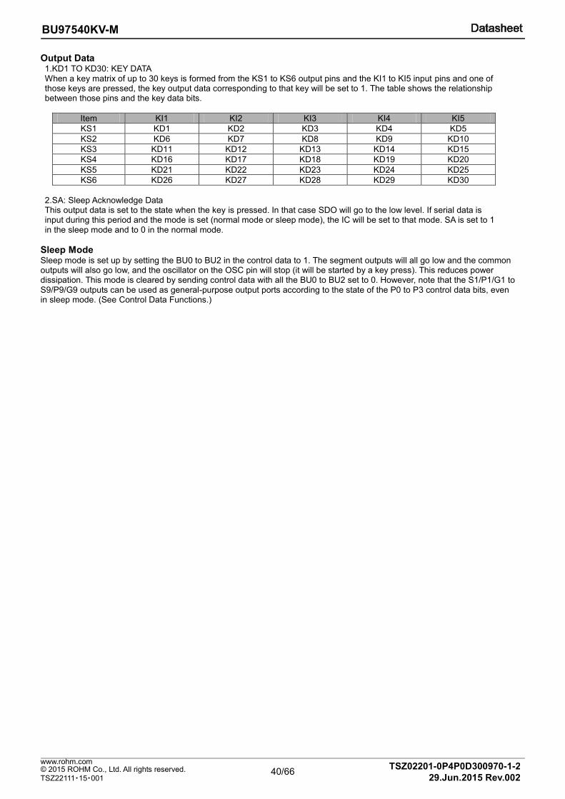
40/66
BU97540KV-M
TSZ02201-0P4P0D300970-1-2 © 2015 ROHM Co., Ltd. All rights reserved. 29.Jun.2015 Rev.002
www.rohm.com
TSZ22111・15・001
Output Data 1.KD1 TO KD30: KEY DATA When a key matrix of up to 30 keys is formed from the KS1 to KS6 output pins and the KI1 to KI5 input pins and one of those keys are pressed, the key output data corresponding to that key will be set to 1. The table shows the relationship between those pins and the key data bits.
Item KI1 KI2 KI3 KI4 KI5
KS1 KD1 KD2 KD3 KD4 KD5
KS2 KD6 KD7 KD8 KD9 KD10
KS3 KD11 KD12 KD13 KD14 KD15
KS4 KD16 KD17 KD18 KD19 KD20
KS5 KD21 KD22 KD23 KD24 KD25
KS6 KD26 KD27 KD28 KD29 KD30
2.SA: Sleep Acknowledge Data This output data is set to the state when the key is pressed. In that case SDO will go to the low level. If serial data is input during this period and the mode is set (normal mode or sleep mode), the IC will be set to that mode. SA is set to 1 in the sleep mode and to 0 in the normal mode.
Sleep Mode
Sleep mode is set up by setting the BU0 to BU2 in the control data to 1. The segment outputs will all go low and the common outputs will also go low, and the oscillator on the OSC pin will stop (it will be started by a key press). This reduces power dissipation. This mode is cleared by sending control data with all the BU0 to BU2 set to 0. However, note that the S1/P1/G1 to S9/P9/G9 outputs can be used as general-purpose output ports according to the state of the P0 to P3 control data bits, even in sleep mode. (See Control Data Functions.)
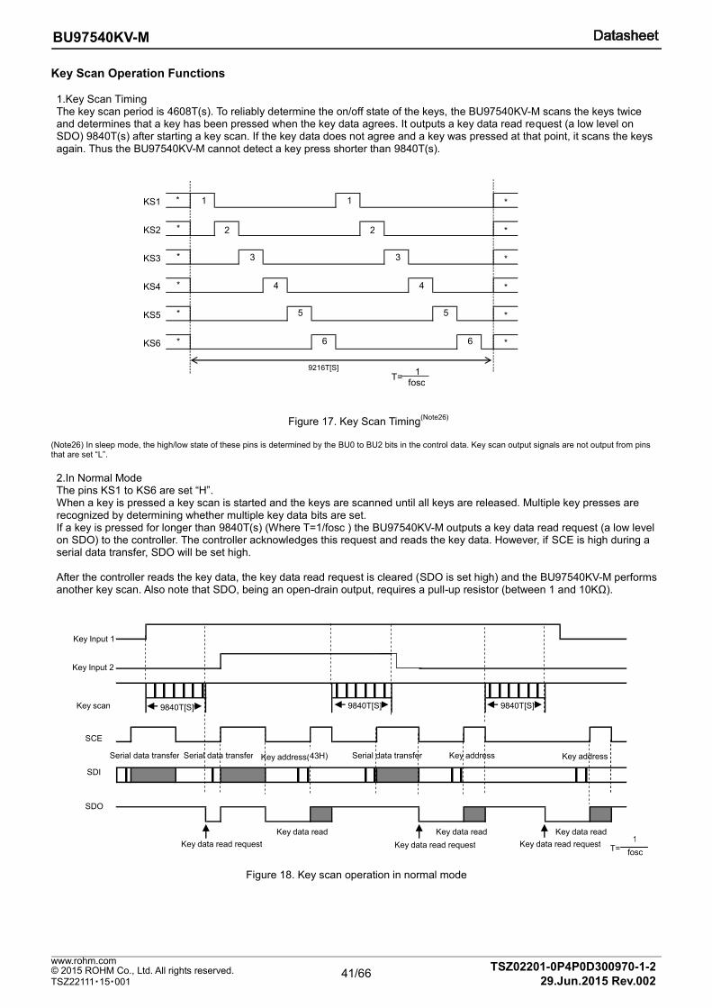
41/66
BU97540KV-M
TSZ02201-0P4P0D300970-1-2 © 2015 ROHM Co., Ltd. All rights reserved. 29.Jun.2015 Rev.002
www.rohm.com
TSZ22111・15・001
KS1
KS2
KS3
KS4
KS5
KS6
9216T[S]
1
2
3
4
5
6
1
2
3
4
5
6
*
*
*
*
* *
*
*
*
*
T=1
fosc
* *
Key Scan Operation Functions 1.Key Scan Timing The key scan period is 4608T(s). To reliably determine the on/off state of the keys, the BU97540KV-M scans the keys twice and determines that a key has been pressed when the key data agrees. It outputs a key data read request (a low level on SDO) 9840T(s) after starting a key scan. If the key data does not agree and a key was pressed at that point, it scans the keys again. Thus the BU97540KV-M cannot detect a key press shorter than 9840T(s).
Figure 17. Key Scan Timing
(Note26)
(Note26) In sleep mode, the high/low state of these pins is determined by the BU0 to BU2 bits in the control data. Key scan output signals are not output from pins that are set “L”.
2.In Normal Mode The pins KS1 to KS6 are set “H”. When a key is pressed a key scan is started and the keys are scanned until all keys are released. Multiple key presses are recognized by determining whether multiple key data bits are set. If a key is pressed for longer than 9840T(s) (Where T=1/fosc ) the BU97540KV-M outputs a key data read request (a low level on SDO) to the controller. The controller acknowledges this request and reads the key data. However, if SCE is high during a serial data transfer, SDO will be set high.
After the controller reads the key data, the key data read request is cleared (SDO is set high) and the BU97540KV-M performs another key scan. Also note that SDO, being an open-drain output, requires a pull-up resistor (between 1 and 10KΩ).
Figure 18. Key scan operation in normal mode
9840T[S] 9840T[S] 9840T[S]
Serial data transfer Serial data transfer Key address(43H) Serial data transfer Key address Key address
Key data read Key data read Key data read
Key data read request Key data read request Key data read requestT=
1
fosc
Key Input 1
Key Input 2
Key scan
CE
DI
D0
43H)
SCE
SDI
SDO
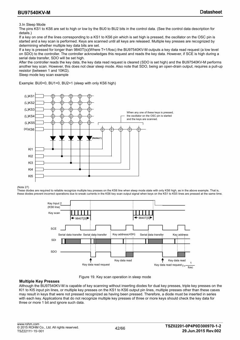
42/66
BU97540KV-M
TSZ02201-0P4P0D300970-1-2 © 2015 ROHM Co., Ltd. All rights reserved. 29.Jun.2015 Rev.002
www.rohm.com
TSZ22111・15・001
3.In Sleep Mode The pins KS1 to KS6 are set to high or low by the BU0 to BU2 bits in the control data. (See the control data description for details.) If a key on one of the lines corresponding to a KS1 to KS6 pin which is set high is pressed, the oscillator on the OSC pin is started and a key scan is performed. Keys are scanned until all keys are released. Multiple key presses are recognized by determining whether multiple key data bits are set. If a key is pressed for longer than 9840T(s)(Where T=1/fosc) the BU97540KV-M outputs a key data read request (a low level on SDO) to the controller. The controller acknowledges this request and reads the key data. However, if SCE is high during a serial data transfer, SDO will be set high. After the controller reads the key data, the key data read request is cleared (SDO is set high) and the BU97540KV-M performs another key scan. However, this does not clear sleep mode. Also note that SDO, being an open-drain output, requires a pull-up resistor (between 1 and 10KΩ). Sleep mode key scan example
Example: BU0=0, BU1=0, BU2=1 (sleep with only KS6 high)
(Note 27) These diodes are required to reliable recognize multiple key presses on the KS6 line when sleep mode state with only KS6 high, as in the above example. That is, these diodes prevent incorrect operations due to sneak currents in the KS6 key scan output signal when keys on the KS1 to KS5 lines are pressed at the same time.
Figure 19. Key scan operation in sleep mode
Multiple Key Presses Although the BU97540KV-M is capable of key scanning without inserting diodes for dual key presses, triple key presses on the KI1 to KI5 input pin lines, or multiple key presses on the KS1 to KS6 output pin lines, multiple presses other than these cases may result in keys that were not pressed recognized as having been pressed. Therefore, a diode must be inserted in series with each key. Applications that do not recognize multiple key presses of three or more keys should check the key data for three or more 1 bit and ignore such data.
9840T[S] 9840T[S]
Serial data transfer Serial data transfer Key address(43H) Serial data transfer Key address
Key data read Key data read
Key data read request Key data read request
Key Input 2
(KS6 line)
Key scan
CE
DI
D0
T=1
fosc
43H)
(L)KS1
(L)KS2
(L)KS3
(L)KS4
(L)KS5
(L)KS6
Kl1
Kl2
Kl3
Kl4
Kl5
When any one of these keys is pressed,
the oscillator on the OSC pin is started
and the keys are scanned.
(H)
SCE
SDI
SDO
(Note27)
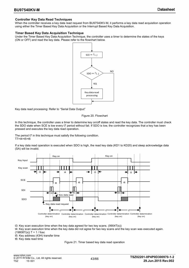
43/66
BU97540KV-M
TSZ02201-0P4P0D300970-1-2 © 2015 ROHM Co., Ltd. All rights reserved. 29.Jun.2015 Rev.002
www.rohm.com
TSZ22111・15・001
SCE =「L 」
SDO =「L 」NO
YES
Key data read processing
Controller Key Data Read Techniques When the controller receives a key data read request from BU97540KV-M, it performs a key data read acquisition operation using either the Timer Based Key Data Acquisition or the Interrupt Based Key Data Acquisition.
Timer Based Key Data Acquisition Technique Under the Timer Based Key Data Acquisition Technique, the controller uses a timer to determine the states of the keys (ON or OFF) and read the key data. Please refer to the flowchart below.
Key data read processing: Refer to “Serial Data Output”
Figure 20. Flowchart
In this technique, the controller uses a timer to determine key on/off states and read the key data. The controller must check the SDO state when SCE is low every t7 period without fail. If SDO is low, the controller recognizes that a key has been pressed and executes the key data read operation.
The period t7 in this technique must satisfy the following condition. T7>t4+t5+t6
If a key data read operation is executed when SDO is high, the read key data (KD1 to KD20) and sleep acknowledge data (SA) will be invalid.
t3 t4
Key on
Controller determination
(key on)
Key Input
Key scan
SCE
SDI
SDO
t3
Key on
t6 t6 t6
t5
t3
t7 t7 t7 t7
Key data readt5 t5
Key data read request
Controller determination
(key on)
Controller determination
(key on)
Controller determination
(key on)
Controller determination
(key on)
t3: Key scan execution time when the key data agreed for two key scans. (9904T(s)) t4: Key scan execution time when the key data did not agree for two key scans and the key scan was executed again. (19808T(s)) T = 1 / fosc t5: Key address (43H) transfer time t6: Key data read time
Figure 21. Timer based key data read operation
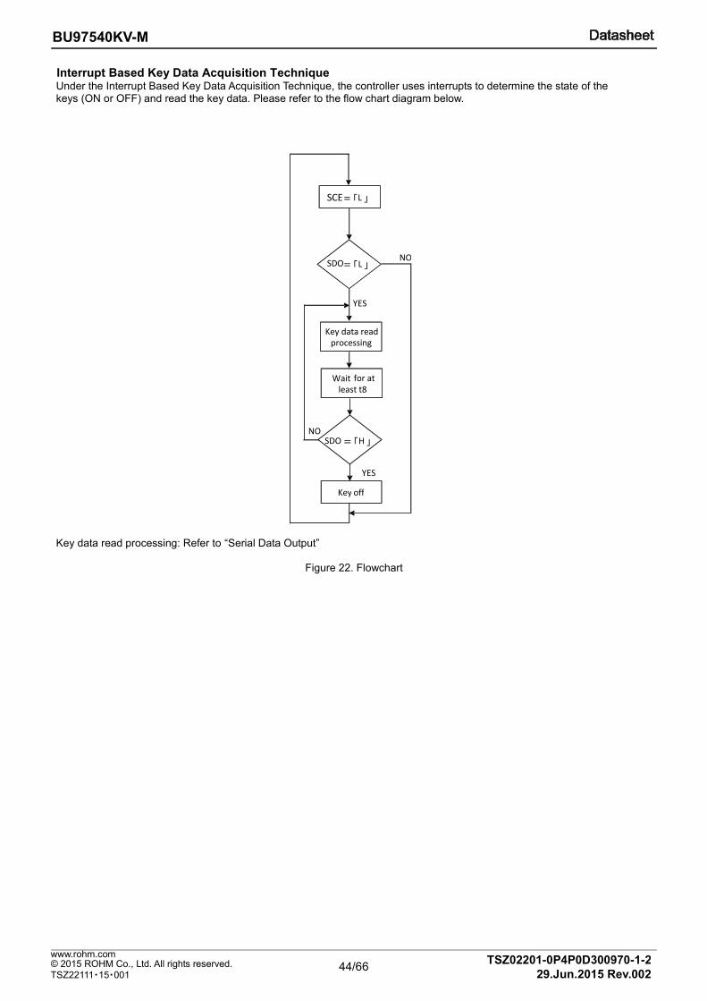
44/66
BU97540KV-M
TSZ02201-0P4P0D300970-1-2 © 2015 ROHM Co., Ltd. All rights reserved. 29.Jun.2015 Rev.002
www.rohm.com
TSZ22111・15・001
Interrupt Based Key Data Acquisition Technique Under the Interrupt Based Key Data Acquisition Technique, the controller uses interrupts to determine the state of the keys (ON or OFF) and read the key data. Please refer to the flow chart diagram below.
Key data read processing: Refer to “Serial Data Output”
Figure 22. Flowchart
CE = 「 L 」
D0 = 「 L 」
Key data read processing
NO
YES
Wait for at least t8
D0 = 「 H 」
Key off
YES
NO
SCE
SDO
SDO
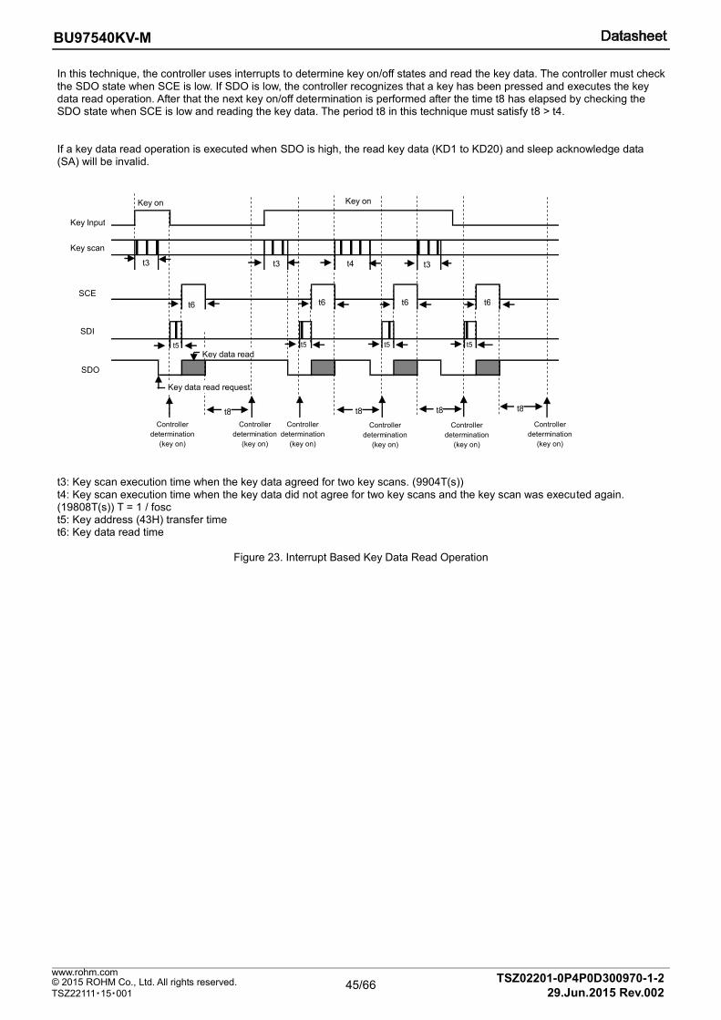
45/66
BU97540KV-M
TSZ02201-0P4P0D300970-1-2 © 2015 ROHM Co., Ltd. All rights reserved. 29.Jun.2015 Rev.002
www.rohm.com
TSZ22111・15・001
In this technique, the controller uses interrupts to determine key on/off states and read the key data. The controller must check the SDO state when SCE is low. If SDO is low, the controller recognizes that a key has been pressed and executes the key data read operation. After that the next key on/off determination is performed after the time t8 has elapsed by checking the SDO state when SCE is low and reading the key data. The period t8 in this technique must satisfy t8 > t4.
If a key data read operation is executed when SDO is high, the read key data (KD1 to KD20) and sleep acknowledge data (SA) will be invalid.
t3 t4
Key on
Controller
determination
(key on)
Key Input
Key scan
SCE
SDI
SDO
t3
Key on
t6 t6 t6
t5
t3
t8
Key data read
t5 t5
Key data read request
Controller
determination
(key on)
Controller
determination
(key on)
Controller
determination
(key on)
Controller
determination
(key on)
t5
t6
t8 t8 t8
Controller
determination
(key on)
t3: Key scan execution time when the key data agreed for two key scans. (9904T(s)) t4: Key scan execution time when the key data did not agree for two key scans and the key scan was executed again. (19808T(s)) T = 1 / fosc t5: Key address (43H) transfer time t6: Key data read time
Figure 23. Interrupt Based Key Data Read Operation
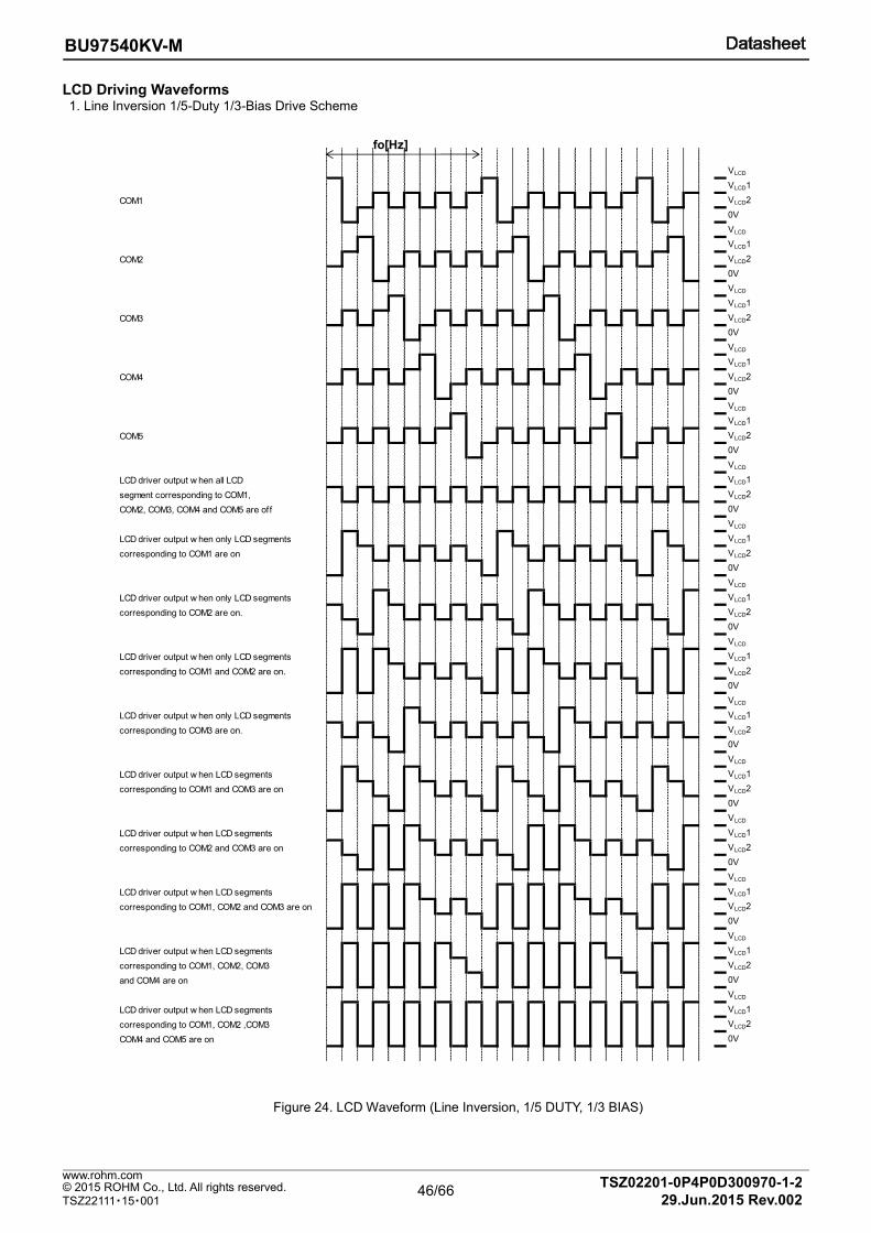
46/66
BU97540KV-M
TSZ02201-0P4P0D300970-1-2 © 2015 ROHM Co., Ltd. All rights reserved. 29.Jun.2015 Rev.002
www.rohm.com
TSZ22111・15・001
LCD Driving Waveforms 1. Line Inversion 1/5-Duty 1/3-Bias Drive Scheme
Figure 24. LCD Waveform (Line Inversion, 1/5 DUTY, 1/3 BIAS)
VLCD
VLCD1
COM1 VLCD2
0V
VLCD
VLCD1
COM2 VLCD2
0V
VLCD
VLCD1
COM3 VLCD2
0V
VLCD
VLCD1
COM4 VLCD2
0V
VLCD
VLCD1
COM5 VLCD2
0V
VLCD
LCD driver output w hen all LCD VLCD1
segment corresponding to COM1, VLCD2
COM2, COM3, COM4 and COM5 are off 0V
VLCD
LCD driver output w hen only LCD segments VLCD1
corresponding to COM1 are on VLCD2
0V
VLCD
LCD driver output w hen only LCD segments VLCD1
corresponding to COM2 are on. VLCD2
0V
VLCD
LCD driver output w hen only LCD segments VLCD1
corresponding to COM1 and COM2 are on. VLCD2
0V
VLCD
LCD driver output w hen only LCD segments VLCD1
corresponding to COM3 are on. VLCD2
0V
VLCD
LCD driver output w hen LCD segments VLCD1
corresponding to COM1 and COM3 are on VLCD2
0V
VLCD
LCD driver output w hen LCD segments VLCD1
corresponding to COM2 and COM3 are on VLCD2
0V
VLCD
LCD driver output w hen LCD segments VLCD1
corresponding to COM1, COM2 and COM3 are on VLCD2
0V
VLCD
LCD driver output w hen LCD segments VLCD1
corresponding to COM1, COM2, COM3 VLCD2
and COM4 are on 0V
VLCD
LCD driver output w hen LCD segments VLCD1
corresponding to COM1, COM2 ,COM3 VLCD2
COM4 and COM5 are on 0V
fo[Hz]
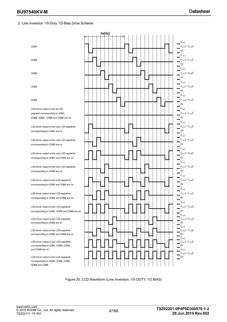
47/66
BU97540KV-M
TSZ02201-0P4P0D300970-1-2 © 2015 ROHM Co., Ltd. All rights reserved. 29.Jun.2015 Rev.002
www.rohm.com
TSZ22111・15・001
2. Line Inversion 1/5-Duty 1/2-Bias Drive Scheme
Figure 25. LCD Waveform (Line Inversion, 1/5 DUTY, 1/2 BIAS)
VLCD
COM1 VLCD1, VLCD2
0V
VLCD
COM2 VLCD1, VLCD2
0V
VLCD
COM3 VLCD1, VLCD2
0V
VLCD
COM4 VLCD1, VLCD2
0V
VLCD
COM5 VLCD1, VLCD2
0V
LCD driver output w hen all LCD VLCD
segment corresponding to COM1, VLCD1, VLCD2
COM2, COM3, COM4 and COM5 are off 0V
VLCD
LCD driver output w hen only LCD segments VLCD1, VLCD2
corresponding to COM1 are on 0V
VLCD
LCD driver output w hen only LCD segments VLCD1, VLCD2
corresponding to COM2 are on. 0V
VLCD
LCD driver output w hen only LCD segments VLCD1, VLCD2
corresponding to COM1 and COM2 are on. 0V
VLCD
LCD driver output w hen only LCD segments VLCD1, VLCD2
corresponding to COM3 are on. 0V
VLCD
LCD driver output w hen LCD segments VLCD1, VLCD2
corresponding to COM1 and COM3 are on 0V
VLCD
LCD driver output w hen LCD segments VLCD1, VLCD2
corresponding to COM2 and COM3 are on 0V
VLCD
LCD driver output w hen LCD segments VLCD1, VLCD2
corresponding to COM1, COM2 and COM3 are on 0V
VLCD
LCD driver output w hen LCD segments VLCD1, VLCD2
corresponding to COM4 are on 0V
VLCD
LCD driver output w hen LCD segments VLCD1, VLCD2
corresponding to COM2 and COM4 are on 0V
VLCD
LCD driver output w hen LCD segments VLCD1, VLCD2
corresponding to COM1, COM2, COM3 0V
and COM4 are on VLCD
VLCD1, VLCD2
LCD driver output w hen LCD segments 0V
corresponding to COM1, COM2, COM3,
COM4 and COM5
fo[Hz]
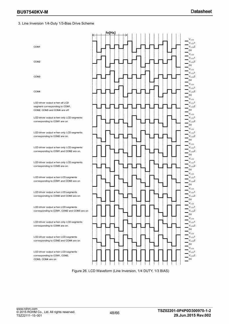
48/66
BU97540KV-M
TSZ02201-0P4P0D300970-1-2 © 2015 ROHM Co., Ltd. All rights reserved. 29.Jun.2015 Rev.002
www.rohm.com
TSZ22111・15・001
3. Line Inversion 1/4-Duty 1/3-Bias Drive Scheme
VLCD
VLCD1
COM1 VLCD2
0V
VLCD
VLCD1
COM2 VLCD2
0V
VLCD
VLCD1
COM3 VLCD2
0V
VLCD
VLCD1
COM4 VLCD2
0V
VLCD
LCD driver output w hen all LCD VLCD1
segment corresponding to COM1, VLCD2
COM2, COM3 and COM4 are off 0V
VLCD
LCD driver output w hen only LCD segments VLCD1
corresponding to COM1 are on VLCD2
0V
VLCD
LCD driver output w hen only LCD segments VLCD1
corresponding to COM2 are on. VLCD2
0V
VLCD
LCD driver output w hen only LCD segments VLCD1
corresponding to COM1 and COM2 are on. VLCD2
0V
VLCD
LCD driver output w hen only LCD segments VLCD1
corresponding to COM3 are on. VLCD2
0V
VLCD
LCD driver output w hen LCD segments VLCD1
corresponding to COM1 and COM3 are on VLCD2
0V
VLCD
LCD driver output w hen LCD segments VLCD1
corresponding to COM2 and COM3 are on VLCD2
0V
VLCD
LCD driver output w hen LCD segments VLCD1
corresponding to COM1, COM2 and COM3 are on VLCD2
0V
VLCD
LCD driver output w hen only LCD segments VLCD1
corresponding to COM4 are on. VLCD2
0V
VLCD
LCD driver output w hen LCD segments VLCD1
corresponding to COM2 and COM4 are on VLCD2
0V
VLCD
LCD driver output w hen LCD segments VLCD1
corresponding to COM1, COM2, VLCD2
COM3, COM4 are on 0V
fo[Hz]
Figure 26. LCD Waveform (Line Inversion, 1/4 DUTY, 1/3 BIAS)
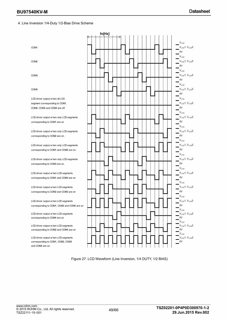
49/66
BU97540KV-M
TSZ02201-0P4P0D300970-1-2 © 2015 ROHM Co., Ltd. All rights reserved. 29.Jun.2015 Rev.002
www.rohm.com
TSZ22111・15・001
4. Line Inversion 1/4-Duty 1/2-Bias Drive Scheme
Figure 27. LCD Waveform (Line Inversion, 1/4 DUTY, 1/2 BIAS)
VLCD
COM1 VLCD1, VLCD2
0V
VLCD
COM2 VLCD1, VLCD2
0V
VLCD
COM3 VLCD1, VLCD2
0V
VLCD
COM4 VLCD1, VLCD2
0V
LCD driver output w hen all LCD VLCD
segment corresponding to COM1, VLCD1, VLCD2
COM2, COM3 and COM4 are off 0V
VLCD
LCD driver output w hen only LCD segments VLCD1, VLCD2
corresponding to COM1 are on 0V
VLCD
LCD driver output w hen only LCD segments VLCD1, VLCD2
corresponding to COM2 are on. 0V
VLCD
LCD driver output w hen only LCD segments VLCD1, VLCD2
corresponding to COM1 and COM2 are on. 0V
VLCD
LCD driver output w hen only LCD segments VLCD1, VLCD2
corresponding to COM3 are on. 0V
VLCD
LCD driver output w hen LCD segments VLCD1, VLCD2
corresponding to COM1 and COM3 are on 0V
VLCD
LCD driver output w hen LCD segments VLCD1, VLCD2
corresponding to COM2 and COM3 are on 0V
VLCD
LCD driver output w hen LCD segments VLCD1, VLCD2
corresponding to COM1, COM2 and COM3 are on 0V
VLCD
LCD driver output w hen LCD segments VLCD1, VLCD2
corresponding to COM4 are on 0V
VLCD
LCD driver output w hen LCD segments VLCD1, VLCD2
corresponding to COM2 and COM4 are on 0V
VLCD
LCD driver output w hen LCD segments VLCD1, VLCD2
corresponding to COM1, COM2, COM3 0V
and COM4 are on
fo[Hz]
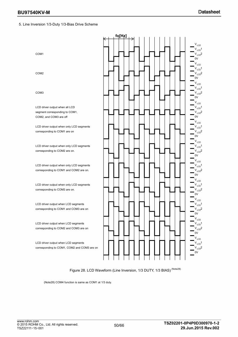
50/66
BU97540KV-M
TSZ02201-0P4P0D300970-1-2 © 2015 ROHM Co., Ltd. All rights reserved. 29.Jun.2015 Rev.002
www.rohm.com
TSZ22111・15・001
5. Line Inversion 1/3-Duty 1/3-Bias Drive Scheme
Figure 28. LCD Waveform (Line Inversion, 1/3 DUTY, 1/3 BIAS) (Note28)
(Note28) COM4 function is same as COM1 at 1/3 duty.
V LCD
V LCD 1
COM1 V LCD 2
0V
V LCD
V LCD 1
COM2 V LCD 2
0V
V LCD
V LCD 1
COM3 V LCD 2
0V
V LCD
LCD driver output when all LCD V LCD 1
segment corresponding to COM1, V LCD 2
COM2, and COM3 are off 0V
V LCD
LCD driver output when only LCD segments V LCD 1
corresponding to COM1 are on V LCD 2
0V
V LCD
LCD driver output when only LCD segments V LCD 1
corresponding to COM2 are on. V LCD 2
0V
V LCD
LCD driver output when only LCD segments V LCD 1
corresponding to COM1 and COM2 are on. V LCD 2
0V
V LCD
LCD driver output when only LCD segments V LCD 1
corresponding to COM3 are on. V LCD 2
0V
V LCD
LCD driver output when LCD segments V LCD 1
corresponding to COM1 and COM3 are on V LCD 2
0V
V LCD
LCD driver output when LCD segments V LCD 1
corresponding to COM2 and COM3 are on V LCD 2
0V
V LCD
LCD driver output when LCD segments V LCD 1
corresponding to COM1, COM2 and COM3 are on V LCD 2
0V
fo[Hz]
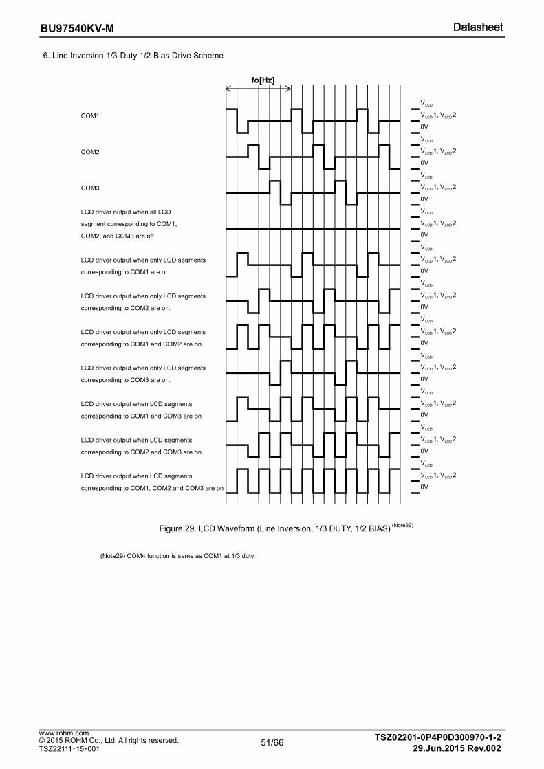
51/66
BU97540KV-M
TSZ02201-0P4P0D300970-1-2 © 2015 ROHM Co., Ltd. All rights reserved. 29.Jun.2015 Rev.002
www.rohm.com
TSZ22111・15・001
6. Line Inversion 1/3-Duty 1/2-Bias Drive Scheme
Figure 29. LCD Waveform (Line Inversion, 1/3 DUTY, 1/2 BIAS)
(Note29)
(Note29) COM4 function is same as COM1 at 1/3 duty.
V LCD
COM1 V LCD 1, V LCD 2
0V
V LCD
COM2 V LCD 1, V LCD 2
0V
V LCD
COM3 V LCD 1, V LCD 2
0V
LCD driver output when all LCD V LCD
segment corresponding to COM1, V LCD 1, V LCD 2
COM2, and COM3 are off 0V
V LCD
LCD driver output when only LCD segments V LCD 1, V LCD 2
corresponding to COM1 are on 0V
V LCD
LCD driver output when only LCD segments V LCD 1, V LCD 2
corresponding to COM2 are on. 0V
V LCD
LCD driver output when only LCD segments V LCD 1, V LCD 2
corresponding to COM1 and COM2 are on. 0V
V LCD
LCD driver output when only LCD segments V LCD 1, V LCD 2
corresponding to COM3 are on. 0V
V LCD
LCD driver output when LCD segments V LCD 1, V LCD 2
corresponding to COM1 and COM3 are on 0V
V LCD
LCD driver output when LCD segments V LCD 1, V LCD 2
corresponding to COM2 and COM3 are on 0V
V LCD
LCD driver output when LCD segments V LCD 1, V LCD 2
corresponding to COM1, COM2 and COM3 are on 0V
fo[Hz]
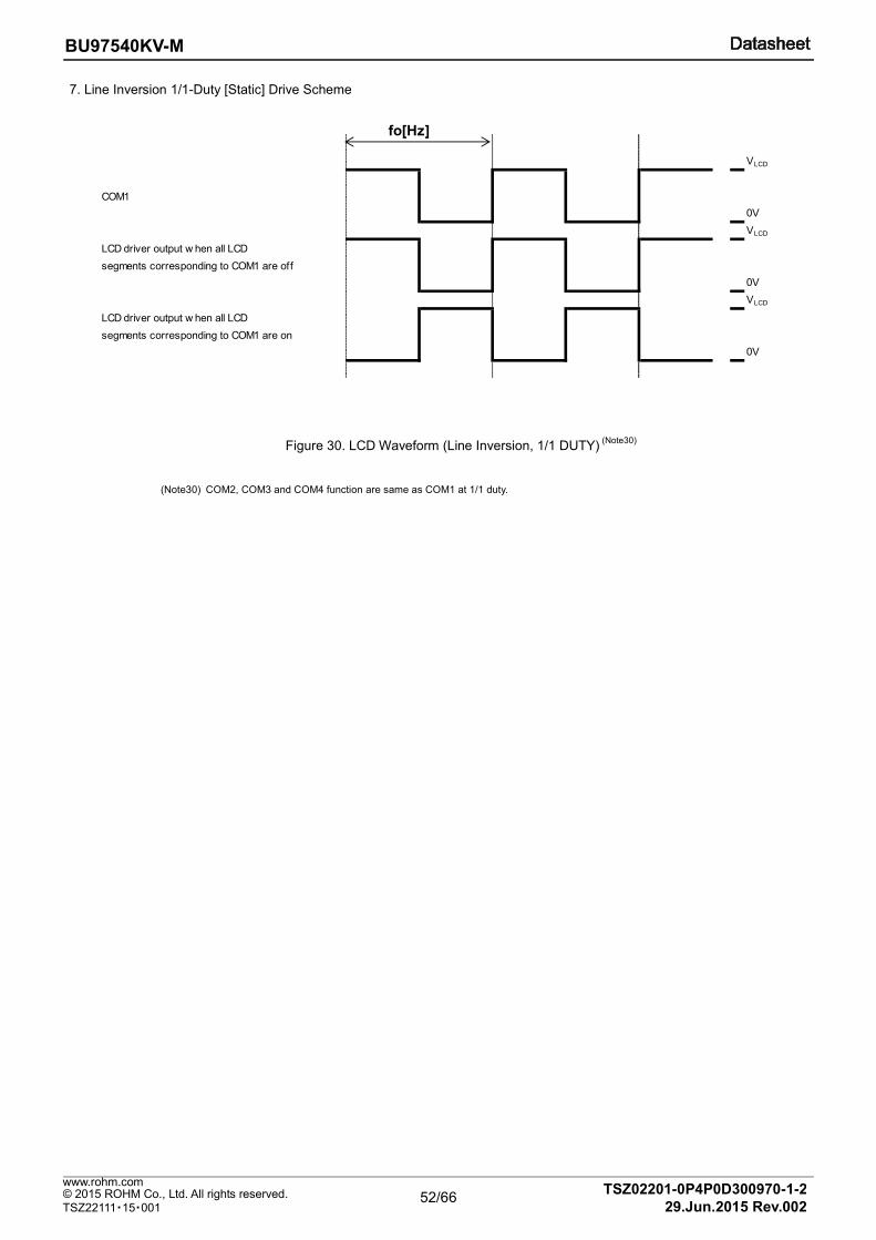
52/66
BU97540KV-M
TSZ02201-0P4P0D300970-1-2 © 2015 ROHM Co., Ltd. All rights reserved. 29.Jun.2015 Rev.002
www.rohm.com
TSZ22111・15・001
7. Line Inversion 1/1-Duty [Static] Drive Scheme
Figure 30. LCD Waveform (Line Inversion, 1/1 DUTY) (Note30)
(Note30) COM2, COM3 and COM4 function are same as COM1 at 1/1 duty.
VLCD
COM1
0V
VLCD
LCD driver output w hen all LCD
segments corresponding to COM1 are off
0V
VLCD
LCD driver output w hen all LCD
segments corresponding to COM1 are on
0V
fo[Hz]
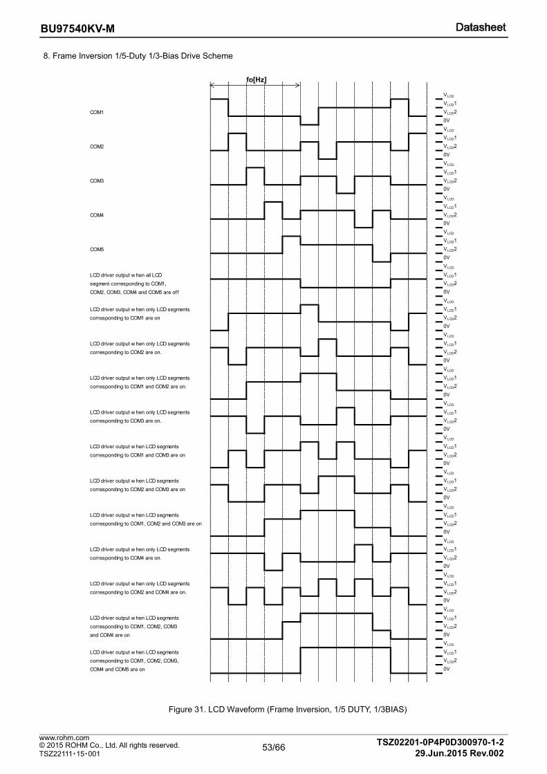
53/66
BU97540KV-M
TSZ02201-0P4P0D300970-1-2 © 2015 ROHM Co., Ltd. All rights reserved. 29.Jun.2015 Rev.002
www.rohm.com
TSZ22111・15・001
8. Frame Inversion 1/5-Duty 1/3-Bias Drive Scheme
VLCD
VLCD1
COM1 VLCD2
0V
VLCD
VLCD1
COM2 VLCD2
0V
VLCD
VLCD1
COM3 VLCD2
0V
VLCD
VLCD1
COM4 VLCD2
0V
VLCD
VLCD1
COM5 VLCD2
0V
VLCD
LCD driver output w hen all LCD VLCD1
segment corresponding to COM1, VLCD2
COM2, COM3, COM4 and COM5 are off 0V
VLCD
LCD driver output w hen only LCD segments VLCD1
corresponding to COM1 are on VLCD2
0V
VLCD
LCD driver output w hen only LCD segments VLCD1
corresponding to COM2 are on. VLCD2
0V
VLCD
LCD driver output w hen only LCD segments VLCD1
corresponding to COM1 and COM2 are on. VLCD2
0V
VLCD
LCD driver output w hen only LCD segments VLCD1
corresponding to COM3 are on. VLCD2
0V
VLCD
LCD driver output w hen LCD segments VLCD1
corresponding to COM1 and COM3 are on VLCD2
0V
VLCD
LCD driver output w hen LCD segments VLCD1
corresponding to COM2 and COM3 are on VLCD2
0V
VLCD
LCD driver output w hen LCD segments VLCD1
corresponding to COM1, COM2 and COM3 are on VLCD2
0V
VLCD
LCD driver output w hen only LCD segments VLCD1
corresponding to COM4 are on. VLCD2
0V
VLCD
LCD driver output w hen only LCD segments VLCD1
corresponding to COM2 and COM4 are on. VLCD2
0V
VLCD
LCD driver output w hen LCD segments VLCD1
corresponding to COM1, COM2, COM3 VLCD2
and COM4 are on 0V
VLCD
LCD driver output w hen LCD segments VLCD1
corresponding to COM1, COM2, COM3, VLCD2
COM4 and COM5 are on 0V
fo[Hz]
Figure 31. LCD Waveform (Frame Inversion, 1/5 DUTY, 1/3BIAS)
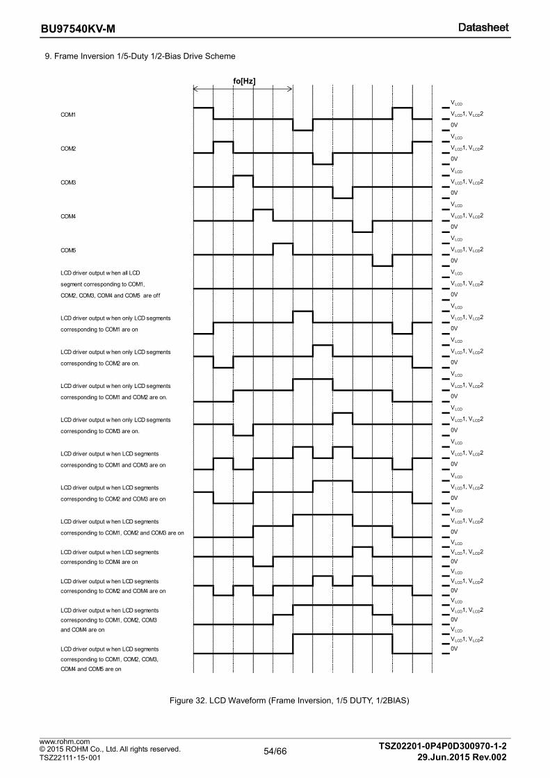
54/66
BU97540KV-M
TSZ02201-0P4P0D300970-1-2 © 2015 ROHM Co., Ltd. All rights reserved. 29.Jun.2015 Rev.002
www.rohm.com
TSZ22111・15・001
9. Frame Inversion 1/5-Duty 1/2-Bias Drive Scheme
VLCD
COM1 VLCD1, VLCD2
0V
VLCD
COM2 VLCD1, VLCD2
0V
VLCD
COM3 VLCD1, VLCD2
0V
VLCD
COM4 VLCD1, VLCD2
0V
VLCD
COM5 VLCD1, VLCD2
0V
LCD driver output w hen all LCD VLCD
segment corresponding to COM1, VLCD1, VLCD2
COM2, COM3, COM4 and COM5 are off 0V
VLCD
LCD driver output w hen only LCD segments VLCD1, VLCD2
corresponding to COM1 are on 0V
VLCD
LCD driver output w hen only LCD segments VLCD1, VLCD2
corresponding to COM2 are on. 0V
VLCD
LCD driver output w hen only LCD segments VLCD1, VLCD2
corresponding to COM1 and COM2 are on. 0V
VLCD
LCD driver output w hen only LCD segments VLCD1, VLCD2
corresponding to COM3 are on. 0V
VLCD
LCD driver output w hen LCD segments VLCD1, VLCD2
corresponding to COM1 and COM3 are on 0V
VLCD
LCD driver output w hen LCD segments VLCD1, VLCD2
corresponding to COM2 and COM3 are on 0V
VLCD
LCD driver output w hen LCD segments VLCD1, VLCD2
corresponding to COM1, COM2 and COM3 are on 0V
VLCD
LCD driver output w hen LCD segments VLCD1, VLCD2
corresponding to COM4 are on 0V
VLCD
LCD driver output w hen LCD segments VLCD1, VLCD2
corresponding to COM2 and COM4 are on 0V
VLCD
LCD driver output w hen LCD segments VLCD1, VLCD2
corresponding to COM1, COM2, COM3 0V
and COM4 are on VLCD
VLCD1, VLCD2
LCD driver output w hen LCD segments 0V
corresponding to COM1, COM2, COM3,
COM4 and COM5 are on
fo[Hz]
Figure 32. LCD Waveform (Frame Inversion, 1/5 DUTY, 1/2BIAS)
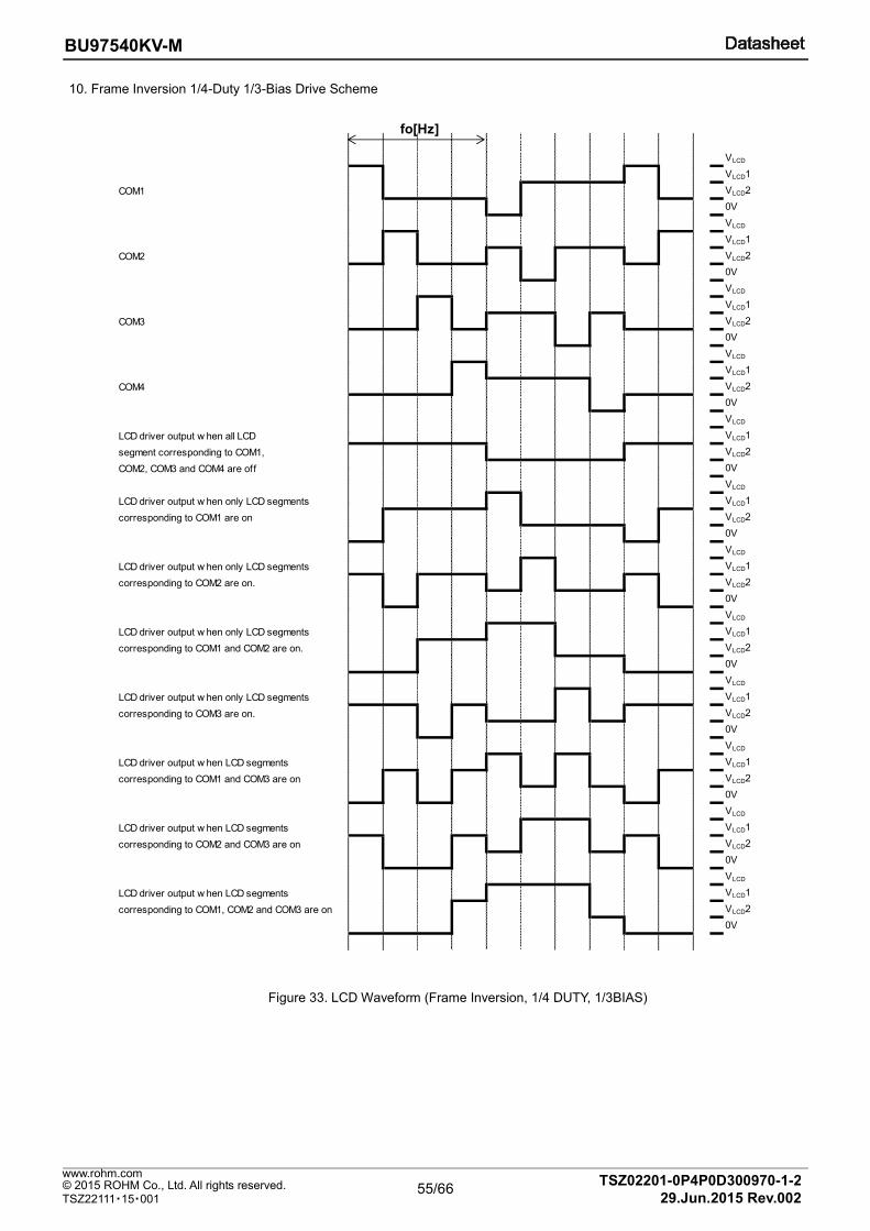
55/66
BU97540KV-M
TSZ02201-0P4P0D300970-1-2 © 2015 ROHM Co., Ltd. All rights reserved. 29.Jun.2015 Rev.002
www.rohm.com
TSZ22111・15・001
10. Frame Inversion 1/4-Duty 1/3-Bias Drive Scheme
Figure 33. LCD Waveform (Frame Inversion, 1/4 DUTY, 1/3BIAS)
VLCD
VLCD1
COM1 VLCD2
0V
VLCD
VLCD1
COM2 VLCD2
0V
VLCD
VLCD1
COM3 VLCD2
0V
VLCD
VLCD1
COM4 VLCD2
0V
VLCD
LCD driver output w hen all LCD VLCD1
segment corresponding to COM1, VLCD2
COM2, COM3 and COM4 are off 0V
VLCD
LCD driver output w hen only LCD segments VLCD1
corresponding to COM1 are on VLCD2
0V
VLCD
LCD driver output w hen only LCD segments VLCD1
corresponding to COM2 are on. VLCD2
0V
VLCD
LCD driver output w hen only LCD segments VLCD1
corresponding to COM1 and COM2 are on. VLCD2
0V
VLCD
LCD driver output w hen only LCD segments VLCD1
corresponding to COM3 are on. VLCD2
0V
VLCD
LCD driver output w hen LCD segments VLCD1
corresponding to COM1 and COM3 are on VLCD2
0V
VLCD
LCD driver output w hen LCD segments VLCD1
corresponding to COM2 and COM3 are on VLCD2
0V
VLCD
LCD driver output w hen LCD segments VLCD1
corresponding to COM1, COM2 and COM3 are on VLCD2
0V
fo[Hz]
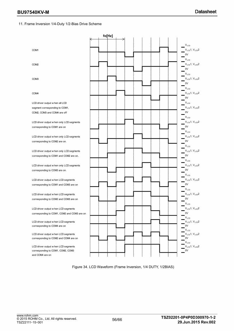
56/66
BU97540KV-M
TSZ02201-0P4P0D300970-1-2 © 2015 ROHM Co., Ltd. All rights reserved. 29.Jun.2015 Rev.002
www.rohm.com
TSZ22111・15・001
11. Frame Inversion 1/4-Duty 1/2-Bias Drive Scheme
Figure 34. LCD Waveform (Frame Inversion, 1/4 DUTY, 1/2BIAS)
VLCD
COM1 VLCD1, VLCD2
0V
VLCD
COM2 VLCD1, VLCD2
0V
VLCD
COM3 VLCD1, VLCD2
0V
VLCD
COM4 VLCD1, VLCD2
0V
LCD driver output w hen all LCD VLCD
segment corresponding to COM1, VLCD1, VLCD2
COM2, COM3 and COM4 are off 0V
VLCD
LCD driver output w hen only LCD segments VLCD1, VLCD2
corresponding to COM1 are on 0V
VLCD
LCD driver output w hen only LCD segments VLCD1, VLCD2
corresponding to COM2 are on. 0V
VLCD
LCD driver output w hen only LCD segments VLCD1, VLCD2
corresponding to COM1 and COM2 are on. 0V
VLCD
LCD driver output w hen only LCD segments VLCD1, VLCD2
corresponding to COM3 are on. 0V
VLCD
LCD driver output w hen LCD segments VLCD1, VLCD2
corresponding to COM1 and COM3 are on 0V
VLCD
LCD driver output w hen LCD segments VLCD1, VLCD2
corresponding to COM2 and COM3 are on 0V
VLCD
LCD driver output w hen LCD segments VLCD1, VLCD2
corresponding to COM1, COM2 and COM3 are on 0V
VLCD
LCD driver output w hen LCD segments VLCD1, VLCD2
corresponding to COM4 are on 0V
VLCD
LCD driver output w hen LCD segments VLCD1, VLCD2
corresponding to COM2 and COM4 are on 0V
VLCD
LCD driver output w hen LCD segments VLCD1, VLCD2
corresponding to COM1, COM2, COM3 0V
and COM4 are on
fo[Hz]
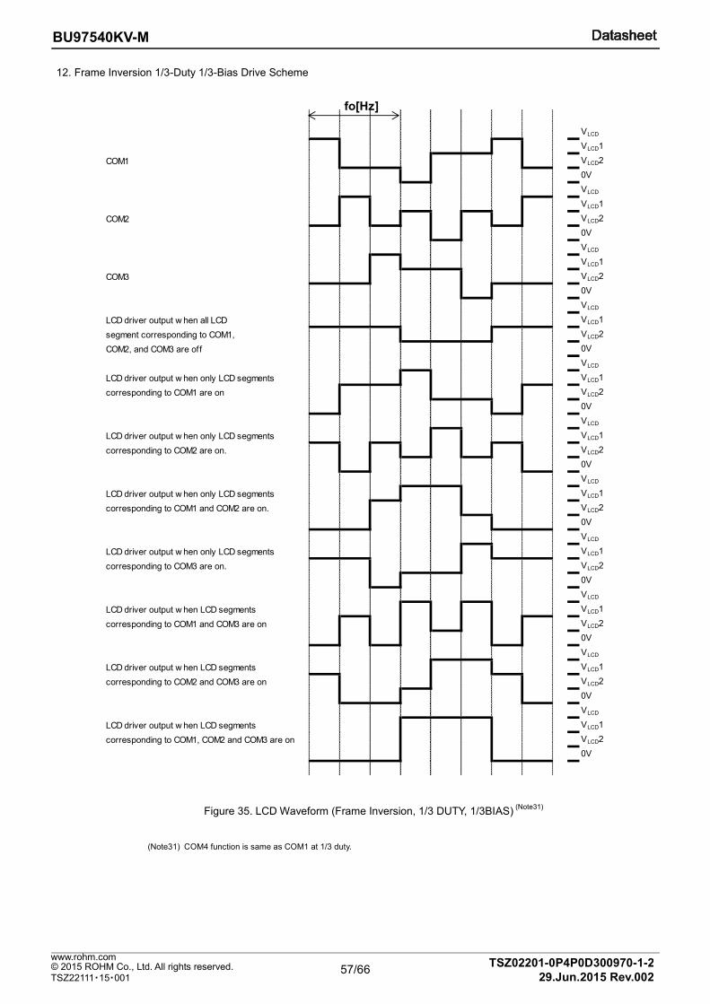
57/66
BU97540KV-M
TSZ02201-0P4P0D300970-1-2 © 2015 ROHM Co., Ltd. All rights reserved. 29.Jun.2015 Rev.002
www.rohm.com
TSZ22111・15・001
12. Frame Inversion 1/3-Duty 1/3-Bias Drive Scheme
VLCD
VLCD1
COM1 VLCD2
0V
VLCD
VLCD1
COM2 VLCD2
0V
VLCD
VLCD1
COM3 VLCD2
0V
VLCD
LCD driver output w hen all LCD VLCD1
segment corresponding to COM1, VLCD2
COM2, and COM3 are off 0V
VLCD
LCD driver output w hen only LCD segments VLCD1
corresponding to COM1 are on VLCD2
0V
VLCD
LCD driver output w hen only LCD segments VLCD1
corresponding to COM2 are on. VLCD2
0V
VLCD
LCD driver output w hen only LCD segments VLCD1
corresponding to COM1 and COM2 are on. VLCD2
0V
VLCD
LCD driver output w hen only LCD segments VLCD1
corresponding to COM3 are on. VLCD2
0V
VLCD
LCD driver output w hen LCD segments VLCD1
corresponding to COM1 and COM3 are on VLCD2
0V
VLCD
LCD driver output w hen LCD segments VLCD1
corresponding to COM2 and COM3 are on VLCD2
0V
VLCD
LCD driver output w hen LCD segments VLCD1
corresponding to COM1, COM2 and COM3 are on VLCD2
0V
fo[Hz]
Figure 35. LCD Waveform (Frame Inversion, 1/3 DUTY, 1/3BIAS)
(Note31)
(Note31) COM4 function is same as COM1 at 1/3 duty.
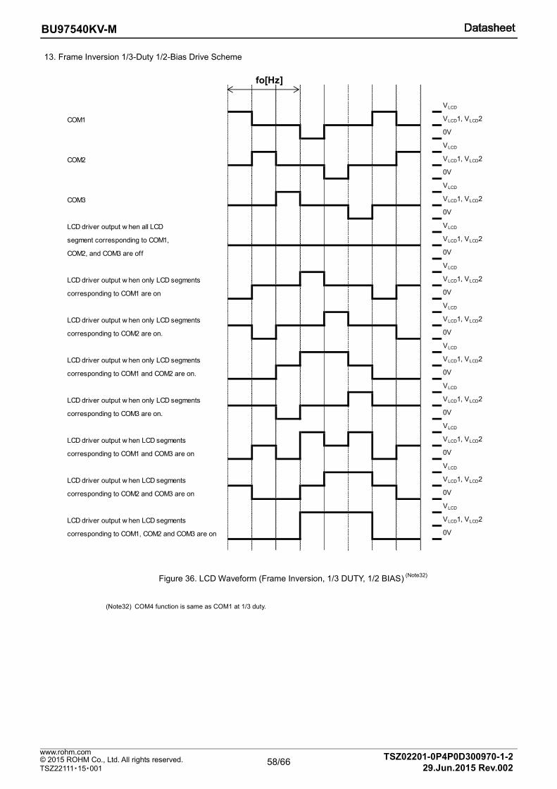
58/66
BU97540KV-M
TSZ02201-0P4P0D300970-1-2 © 2015 ROHM Co., Ltd. All rights reserved. 29.Jun.2015 Rev.002
www.rohm.com
TSZ22111・15・001
13. Frame Inversion 1/3-Duty 1/2-Bias Drive Scheme
VLCD
COM1 VLCD1, VLCD2
0V
VLCD
COM2 VLCD1, VLCD2
0V
VLCD
COM3 VLCD1, VLCD2
0V
LCD driver output w hen all LCD VLCD
segment corresponding to COM1, VLCD1, VLCD2
COM2, and COM3 are off 0V
VLCD
LCD driver output w hen only LCD segments VLCD1, VLCD2
corresponding to COM1 are on 0V
VLCD
LCD driver output w hen only LCD segments VLCD1, VLCD2
corresponding to COM2 are on. 0V
VLCD
LCD driver output w hen only LCD segments VLCD1, VLCD2
corresponding to COM1 and COM2 are on. 0V
VLCD
LCD driver output w hen only LCD segments VLCD1, VLCD2
corresponding to COM3 are on. 0V
VLCD
LCD driver output w hen LCD segments VLCD1, VLCD2
corresponding to COM1 and COM3 are on 0V
VLCD
LCD driver output w hen LCD segments VLCD1, VLCD2
corresponding to COM2 and COM3 are on 0V
VLCD
LCD driver output w hen LCD segments VLCD1, VLCD2
corresponding to COM1, COM2 and COM3 are on 0V
fo[Hz]
Figure 36. LCD Waveform (Frame Inversion, 1/3 DUTY, 1/2 BIAS) (Note32)
(Note32) COM4 function is same as COM1 at 1/3 duty.
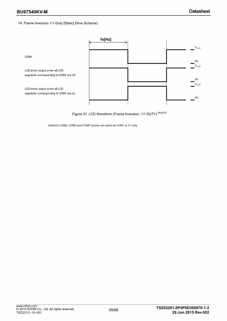
59/66
BU97540KV-M
TSZ02201-0P4P0D300970-1-2 © 2015 ROHM Co., Ltd. All rights reserved. 29.Jun.2015 Rev.002
www.rohm.com
TSZ22111・15・001
14. Frame Inversion 1/1-Duty [Static] Drive Scheme)
Figure 37. LCD Waveform (Frame Inversion, 1/1 DUTY) (Note33)
(Note33) COM2, COM3 and COM4 function are same as COM1 at 1/1 duty.
VLCD
COM1
0V
VLCD
LCD driver output w hen all LCD
segments corresponding to COM1 are off
0V
VLCD
LCD driver output w hen all LCD
segments corresponding to COM1 are on
0V
fo[Hz]
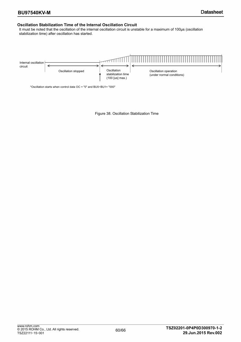
60/66
BU97540KV-M
TSZ02201-0P4P0D300970-1-2 © 2015 ROHM Co., Ltd. All rights reserved. 29.Jun.2015 Rev.002
www.rohm.com
TSZ22111・15・001
Oscillation Stabilization Time of the Internal Oscillation Circuit It must be noted that the oscillation of the internal oscillation circuit is unstable for a maximum of 100μs (oscillation stabilization time) after oscillation has started.
Figure 38. Oscillation Stabilization Time
Oscillation
stabilization time
(100 [us] max.)
Oscillation stopped Oscillation operation
(under normal conditions)
<Oscillation start>
1.If the INHb pin status is switched from "L" to "H"
when control data OC = "0" and BU0~ ="0"
2.If the contorol data BU is set from "1" to "0"
when INHb = "H" and contorol data OC ="0"
Internal oscillation
circuit
*Oscillation starts when control data OC = "0" and BU0~BU1= "000"
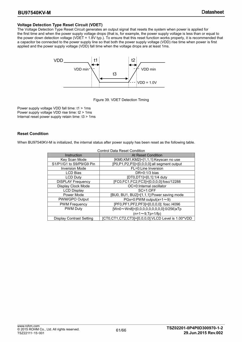
61/66
BU97540KV-M
TSZ02201-0P4P0D300970-1-2 © 2015 ROHM Co., Ltd. All rights reserved. 29.Jun.2015 Rev.002
www.rohm.com
TSZ22111・15・001
Voltage Detection Type Reset Circuit (VDET) The Voltage Detection Type Reset Circuit generates an output signal that resets the system when power is applied for the first time and when the power supply voltage drops (that is, for example, the power supply voltage is less than or equal to the power down detection voltage (VDET = 1.8V typ.). To ensure that this reset function works properly, it is recommended that a capacitor be connected to the power supply line so that both the power supply voltage (VDD) rise time when power is first applied and the power supply voltage (VDD) fall time when the voltage drops are at least 1ms.
t2VDD
VDD min
VDD = 1.0V
VDD min
t1
t3
Figure 39. VDET Detection Timing
Power supply voltage VDD fall time: t1 > 1ms Power supply voltage VDD rise time: t2 > 1ms Internal reset power supply retain time: t3 > 1ms
Reset Condition When BU97540KV-M is initialized, the internal status after power supply has been reset as the following table.
Control Data Reset Condition
Instruction At Reset Condition
Key Scan Mode [KM0,KM1,KM2]=[1,1,1]:Keyscan no use
S1/P1/G1 to S9/P9/G9 Pin [P0,P1,P2,P3]=[0,0,0,0]:all segment output
Inversion Mode FL=0:Line Inversion
LCD Bias DR=0:1/3 bias
LCD Duty [DT0,DT1]=[0,1]:1/4 duty
DISPLAY Frequency [FC0,FC1,FC2,FC3]=[0,0,0,0]:fosc/12288
Display Clock Mode OC=0:Internal oscillator
LCD Display SC=1:OFF
Power Mode [BU0, BU1, BU2]=[1,1,1]:Power saving mode
PWM/GPO Output PGx=0:PWM output(x=1~9)
PWM Frequency [PF0,PF1,PF2,PF3]=[0,0,0,0]: fosc /4096
PWM Duty [Wn0~Wn8]=[0,0,0,0,0,0,0,0,0]:0/256)xTp
(n=1~9,Tp=1/fp)
Display Contrast Setting [CT0,CT1,CT2,CT3]=[0,0,0,0]:VLCD Level is 1.00*VDD
62/66
BU97540KV-M
TSZ02201-0P4P0D300970-1-2 © 2015 ROHM Co., Ltd. All rights reserved. 29.Jun.2015 Rev.002
www.rohm.com
TSZ22111・15・001
Operational Notes
1. Reverse Connection of Power Supply
Connecting the power supply in reverse polarity can damage the IC. Take precautions against reverse polarity when connecting the power supply, such as mounting an external diode between the power supply and the IC’s power supply pins.
2. Power Supply Lines
Design the PCB layout pattern to provide low impedance supply lines. Separate the ground and supply lines of the digital and analog blocks to prevent noise in the ground and supply lines of the digital block from affecting the analog block. Furthermore, connect a capacitor to ground at all power supply pins. Consider the effect of temperature and aging on the capacitance value when using electrolytic capacitors.
3. Ground Voltage
Ensure that no pins are at a voltage below that of the ground pin at any time, even during transient condition.
4. Ground Wiring Pattern
When using both small-signal and large-current ground traces, the two ground traces should be routed separately but connected to a single ground at the reference point of the application board to avoid fluctuations in the small-signal ground caused by large currents. Also ensure that the ground traces of external components do not cause variations on the ground voltage. The ground lines must be as short and thick as possible to reduce line impedance.
5. Thermal Consideration
Should by any chance the power dissipation rating be exceeded the rise in temperature of the chip may result in
deterioration of the properties of the chip. The absolute maximum rating of the Pd stated in this specification is when
the IC is mounted on a 70mm x 70mm x 1.6mm glass epoxy board. In case of exceeding this absolute maximum
rating, increase the board size and copper area to prevent exceeding the Pd rating.
6. Recommended Operating Conditions
These conditions represent a range within which the expected characteristics of the IC can be approximately obtained. The electrical characteristics are guaranteed under the conditions of each parameter.
7. Inrush Current
When power is first supplied to the IC, it is possible that the internal logic may be unstable and inrush current may flow instantaneously due to the internal powering sequence and delays, especially if the IC has more than one power supply. Therefore, give special consideration to power coupling capacitance, power wiring, width of ground wiring, and routing of connections.
8. Operation Under Strong Electromagnetic Field
Operating the IC in the presence of a strong electromagnetic field may cause the IC to malfunction.
9. Testing on Application Boards
When testing the IC on an application board, connecting a capacitor directly to a low-impedance output pin may subject the IC to stress. Always discharge capacitors completely after each process or step. The IC’s power supply should always be turned off completely before connecting or removing it from the test setup during the inspection process. To prevent damage from static discharge, ground the IC during assembly and use similar precautions during transport and storage.
10. Inter-pin Short and Mounting Errors
Ensure that the direction and position are correct when mounting the IC on the PCB. Incorrect mounting may result in damaging the IC. Avoid nearby pins being shorted to each other especially to ground, power supply and output pin. Inter-pin shorts could be due to many reasons such as metal particles, water droplets (in very humid environment) and unintentional solder bridge deposited in between pins during assembly to name a few.
63/66
BU97540KV-M
TSZ02201-0P4P0D300970-1-2 © 2015 ROHM Co., Ltd. All rights reserved. 29.Jun.2015 Rev.002
www.rohm.com
TSZ22111・15・001
Operational Notes – continued
11. Unused Input Pins
Input pins of an IC are often connected to the gate of a MOS transistor. The gate has extremely high impedance and extremely low capacitance. If left unconnected, the electric field from the outside can easily charge it. The small charge acquired in this way is enough to produce a significant effect on the conduction through the transistor and cause unexpected operation of the IC. So unless otherwise specified, unused input pins should be connected to the power supply or ground line.
12. Regarding the Input Pin of the IC
In the construction of this IC, P-N junctions are inevitably formed creating parasitic diodes or transistors. The operation of these parasitic elements can result in mutual interference among circuits, operational faults, or physical damage. Therefore, conditions which cause these parasitic elements to operate, such as applying a voltage to an input pin lower than the ground voltage should be avoided. Furthermore, do not apply a voltage to the input pins when no power supply voltage is applied to the IC. Even if the power supply voltage is applied, make sure that the input pins have voltages within the values specified in the electrical characteristics of this IC.
13. Data transmission
To refrain from data transmission is strongly recommended while power supply is rising up or falling down to prevent from the occurrence of disturbances on transmission and reception.
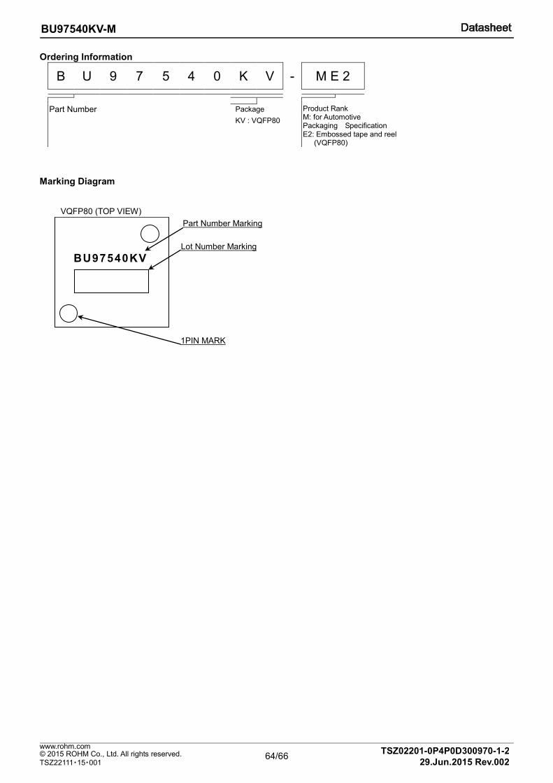
64/66
BU97540KV-M
TSZ02201-0P4P0D300970-1-2 © 2015 ROHM Co., Ltd. All rights reserved. 29.Jun.2015 Rev.002
www.rohm.com
TSZ22111・15・001
Ordering Information
B U 9 7 5 4 0 K V - M E 2
Part Number Package Product Rank M: for Automotive Packaging Specification E2: Embossed tape and reel
(VQFP80)
KV : VQFP80
Marking Diagram
VQFP80 (TOP VIEW)
BU97540KV
Part Number Marking
1PIN MARK
Lot Number Marking
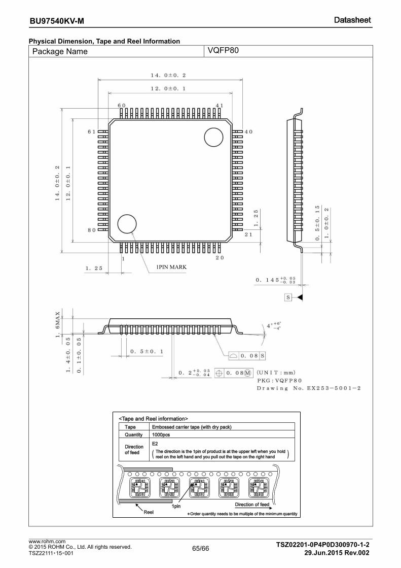
65/66
BU97540KV-M
TSZ02201-0P4P0D300970-1-2 © 2015 ROHM Co., Ltd. All rights reserved. 29.Jun.2015 Rev.002
www.rohm.com
TSZ22111・15・001
Physical Dimension, Tape and Reel Information
Package Name VQFP80
1PIN MARK
66/66
BU97540KV-M
TSZ02201-0P4P0D300970-1-2 © 2015 ROHM Co., Ltd. All rights reserved. 29.Jun.2015 Rev.002
www.rohm.com
TSZ22111・15・001
Revision History
Date Revision Changes
02.Jun.2015 001 New Release
29.Jun.2015 002 Modified Typical Application Circuit in Page2. Modified S66/TESTIN Pin description(Handling when unused) in Page 7. Modified comment of figure.39 in Page 61.

DatasheetDatasheet
Notice-PAA-E Rev.001© 2015 ROHM Co., Ltd. All rights reserved.
Notice Precaution on using ROHM Products
1. If you intend to use our Products in devices requiring extremely high reliability (such as medical equipment (Note 1), aircraft/spacecraft, nuclear power controllers, etc.) and whose malfunction or failure may cause loss of human life, bodily injury or serious damage to property (“Specific Applications”), please consult with the ROHM sales representative in advance. Unless otherwise agreed in writing by ROHM in advance, ROHM shall not be in any way responsible or liable for any damages, expenses or losses incurred by you or third parties arising from the use of any ROHM’s Products for Specific Applications.
(Note1) Medical Equipment Classification of the Specific Applications JAPAN USA EU CHINA
CLASSⅢ CLASSⅢ
CLASSⅡb CLASSⅢ
CLASSⅣ CLASSⅢ
2. ROHM designs and manufactures its Products subject to strict quality control system. However, semiconductor
products can fail or malfunction at a certain rate. Please be sure to implement, at your own responsibilities, adequate safety measures including but not limited to fail-safe design against the physical injury, damage to any property, which a failure or malfunction of our Products may cause. The following are examples of safety measures:
[a] Installation of protection circuits or other protective devices to improve system safety [b] Installation of redundant circuits to reduce the impact of single or multiple circuit failure
3. Our Products are not designed under any special or extraordinary environments or conditions, as exemplified below. Accordingly, ROHM shall not be in any way responsible or liable for any damages, expenses or losses arising from the use of any ROHM’s Products under any special or extraordinary environments or conditions. If you intend to use our Products under any special or extraordinary environments or conditions (as exemplified below), your independent verification and confirmation of product performance, reliability, etc, prior to use, must be necessary:
[a] Use of our Products in any types of liquid, including water, oils, chemicals, and organic solvents [b] Use of our Products outdoors or in places where the Products are exposed to direct sunlight or dust [c] Use of our Products in places where the Products are exposed to sea wind or corrosive gases, including Cl2,
H2S, NH3, SO2, and NO2
[d] Use of our Products in places where the Products are exposed to static electricity or electromagnetic waves [e] Use of our Products in proximity to heat-producing components, plastic cords, or other flammable items [f] Sealing or coating our Products with resin or other coating materials [g] Use of our Products without cleaning residue of flux (even if you use no-clean type fluxes, cleaning residue of
flux is recommended); or Washing our Products by using water or water-soluble cleaning agents for cleaning residue after soldering
[h] Use of the Products in places subject to dew condensation
4. The Products are not subject to radiation-proof design. 5. Please verify and confirm characteristics of the final or mounted products in using the Products. 6. In particular, if a transient load (a large amount of load applied in a short period of time, such as pulse. is applied,
confirmation of performance characteristics after on-board mounting is strongly recommended. Avoid applying power exceeding normal rated power; exceeding the power rating under steady-state loading condition may negatively affect product performance and reliability.
7. De-rate Power Dissipation (Pd) depending on Ambient temperature (Ta). When used in sealed area, confirm the actual
ambient temperature. 8. Confirm that operation temperature is within the specified range described in the product specification. 9. ROHM shall not be in any way responsible or liable for failure induced under deviant condition from what is defined in
this document.
Precaution for Mounting / Circuit board design 1. When a highly active halogenous (chlorine, bromine, etc.) flux is used, the residue of flux may negatively affect product
performance and reliability. 2. In principle, the reflow soldering method must be used on a surface-mount products, the flow soldering method must
be used on a through hole mount products. If the flow soldering method is preferred on a surface-mount products, please consult with the ROHM representative in advance.
For details, please refer to ROHM Mounting specification

DatasheetDatasheet
Notice-PAA-E Rev.001© 2015 ROHM Co., Ltd. All rights reserved.
Precautions Regarding Application Examples and External Circuits 1. If change is made to the constant of an external circuit, please allow a sufficient margin considering variations of the
characteristics of the Products and external components, including transient characteristics, as well as static characteristics.
2. You agree that application notes, reference designs, and associated data and information contained in this document
are presented only as guidance for Products use. Therefore, in case you use such information, you are solely responsible for it and you must exercise your own independent verification and judgment in the use of such information contained in this document. ROHM shall not be in any way responsible or liable for any damages, expenses or losses incurred by you or third parties arising from the use of such information.
Precaution for Electrostatic
This Product is electrostatic sensitive product, which may be damaged due to electrostatic discharge. Please take proper caution in your manufacturing process and storage so that voltage exceeding the Products maximum rating will not be applied to Products. Please take special care under dry condition (e.g. Grounding of human body / equipment / solder iron, isolation from charged objects, setting of Ionizer, friction prevention and temperature / humidity control).
Precaution for Storage / Transportation 1. Product performance and soldered connections may deteriorate if the Products are stored in the places where:
[a] the Products are exposed to sea winds or corrosive gases, including Cl2, H2S, NH3, SO2, and NO2 [b] the temperature or humidity exceeds those recommended by ROHM [c] the Products are exposed to direct sunshine or condensation [d] the Products are exposed to high Electrostatic
2. Even under ROHM recommended storage condition, solderability of products out of recommended storage time period may be degraded. It is strongly recommended to confirm solderability before using Products of which storage time is exceeding the recommended storage time period.
3. Store / transport cartons in the correct direction, which is indicated on a carton with a symbol. Otherwise bent leads
may occur due to excessive stress applied when dropping of a carton. 4. Use Products within the specified time after opening a humidity barrier bag. Baking is required before using Products of
which storage time is exceeding the recommended storage time period.
Precaution for Product Label QR code printed on ROHM Products label is for ROHM’s internal use only.
Precaution for Disposition When disposing Products please dispose them properly using an authorized industry waste company.
Precaution for Foreign Exchange and Foreign Trade act Since concerned goods might be fallen under listed items of export control prescribed by Foreign exchange and Foreign trade act, please consult with ROHM in case of export.
Precaution Regarding Intellectual Property Rights 1. All information and data including but not limited to application example contained in this document is for reference
only. ROHM does not warrant that foregoing information or data will not infringe any intellectual property rights or any other rights of any third party regarding such information or data.
2. ROHM shall not have any obligations where the claims, actions or demands arising from the combination of the Products with other articles such as components, circuits, systems or external equipment (including software).
3. No license, expressly or implied, is granted hereby under any intellectual property rights or other rights of ROHM or any third parties with respect to the Products or the information contained in this document. Provided, however, that ROHM will not assert its intellectual property rights or other rights against you or your customers to the extent necessary to manufacture or sell products containing the Products, subject to the terms and conditions herein.
Other Precaution 1. This document may not be reprinted or reproduced, in whole or in part, without prior written consent of ROHM.
2. The Products may not be disassembled, converted, modified, reproduced or otherwise changed without prior written consent of ROHM.
3. In no event shall you use in any way whatsoever the Products and the related technical information contained in the Products or this document for any military purposes, including but not limited to, the development of mass-destruction weapons.
4. The proper names of companies or products described in this document are trademarks or registered trademarks of ROHM, its affiliated companies or third parties.

DatasheetDatasheet
Notice – WE Rev.001© 2015 ROHM Co., Ltd. All rights reserved.
General Precaution 1. Before you use our Pro ducts, you are requested to care fully read this document and fully understand its contents.
ROHM shall n ot be in an y way responsible or liabl e for fa ilure, malfunction or acci dent arising from the use of a ny ROHM’s Products against warning, caution or note contained in this document.
2. All information contained in this docume nt is current as of the issuing date and subj ect to change without any prior
notice. Before purchasing or using ROHM’s Products, please confirm the la test information with a ROHM sale s representative.
3. The information contained in this doc ument is provi ded on an “as is” basis and ROHM does not warrant that all
information contained in this document is accurate an d/or error-free. ROHM shall not be in an y way responsible or liable for any damages, expenses or losses incurred by you or third parties resulting from inaccuracy or errors of or concerning such information.
Related Documents