i THESIS FOR THE DEGREE OF DOCTOR OF PHILOSOPHY Carbon nanomaterial-based interconnects, integrated capacitors and supercapacitors MUHAMMAD AMIN SALEEM Department of Microtechnology and Nanoscience CHALMERS UNIVERSITY OF TECHNOLOGY Göteborg, Sweden 2017

Welcome message from author
This document is posted to help you gain knowledge. Please leave a comment to let me know what you think about it! Share it to your friends and learn new things together.
Transcript

i
THESIS FOR THE DEGREE OF DOCTOR OF PHILOSOPHY
Carbon nanomaterial-based interconnects,
integrated capacitors and supercapacitors
MUHAMMAD AMIN SALEEM
Department of Microtechnology and Nanoscience
CHALMERS UNIVERSITY OF TECHNOLOGY
Göteborg, Sweden 2017

ii
Carbon nanomaterial-based interconnects, integrated capacitors and supercapacitors
MUHAMMAD AMIN SALEEM
ISBN 978-91-7597-588-7
© MUHAMMAD AMIN SALEEM, 2017
Doktorsavhandlingar vid Chalmers tekniska högskola
Ny series nr 4269
ISSN 0346-718X
Electronics Materials and Systems Laboratory
Department of Microtechnology and Nanoscience
Chalmers University of Technology
SE-412 96 Göteborg, Sweden
Telephone + 46 (0)31-772 1000
Technical report MC2-364
ISSN 1652-0769
Cover: Top to bottom, left to right: Carbon structures based interconnects, Interdigitated
supercapacitor’s pattern, composite and Integrated solid-stat capacitor.
Printed by Chalmers Reproservice
Göteborg, Sweden 2017

iii
Carbon nanomaterial-based interconnects, integrated capacitors and supercapacitors
MUHAMMAD AMIN SALEEM
Department of Microtechnology and Nanoscience
Chalmers University of Technology
ABSTRACT
The constant miniaturization and steady performance improvement of electronics devices have
generated innovative ideas such as internet of thing (IoT), which also includes devices with integrated
energy sources.
The high performance is conceived by the high density of the devices on a chip leading to a high
density of interconnects, to connect these devices to outside world. Since the size and the pitch of the
interconnects have decreased, the current density in interconnect has increased, posing challenges on
the existing copper pillar interconnect technology, such as intermetallic compound formation and
electro-migration resulting in open circuit. The challenges are forecasted to increase on further down
scaling due to bridging of the solder between pillars. Moreover, the environmental pollution and the
threat of vanishing of fossil fuel have prompted to find cheap and efficient alternating energy sources
and energy storage systems.
Carbon nanomaterials such as carbon nanotubes and carbon nanofibers have unprecedented
electrical, mechanical and thermal properties, high resistance to corrosion and high surface area have
been proposed for the solution of above mentioned challenges.
In this thesis, vertically aligned carbon nanofibers (VACNFs) have been grown by direct current
plasma enhanced chemical vapor deposition (dc-PECVD) at complementary metal oxide
semiconductor (CMOS) compatible temperatures for on chip application. In addition, the catalyst to
grow VACNFs is deposited using innovative low-cost polymer–Pd nanohybrid colloidal solutions by
an effective coating method.
Also, due to controllable DC behavior and good mechanical reinforcement properties of solder-
CNFs, the solderable micro-bumps of VACNFs have been shown to potentially yield the acceptable
electrical resistances. Moreover the CNFs bumps can be made in submicron size range, which can
comply with further down scaling of interconnect. In addition, advanced CNF based adhesives,
produced by coating CNFs with low temperature polymers, have been investigated as alternating
anisotropic conducting film for anisotropic connection, using a thermo-compression bonding. The
shearing strength of the bonded chip qualifies the MIL-STD-883 standards of bonding strength in
microelectronics devices.
Further, supercapacitor are the energy storage devices having high energy density, and high power
density due to quick intake and release of charges and long cycles life of about 1 million. On-chip
integrated solid-state parallel-plate capacitor and supercapacitor are demonstrated based on VACNFs.
The preliminary capacitance of the parallel-plate capacitor and supercapacitor are 10-15 nF/mm2 and
10 µF/mm2, respectively. The profile of parallel plate capacitor is below 10 micrometers, which
enables integration even in advance 2.5 and 3D heterogeneous packaging. The on-chip capacitor can
work as decoupling capacitor to resolve the energy fluctuation related issues and also power up
devices on the chip.
Then, along with other properties, high aspect ratio and ease of fabrication, the carbon nanotubes
(CNTs) are considered as potential electrode material for future high performance supercapacitor. The
CNTs are directly grown on electrospun CNFs giving the specific capacitance of 92 F/g, i.e twice the
capacitance of bare CNFs. Finally, a complete energy storage device coin-cell supercapacitor is made
by directly growing VACNFs on the current collector and the capacitance is 15 times higher than the
capacitance without CNFs. Thus such supercapcaitor is suitable to be combined with harvester to
collect energy to the level of operating power of the devices and can provide durable solution to the
frequent change of battery in the devices mounted at sensitive or airborne locations.
Keywords: vertically aligned carbon nanofibers, carbon nanotubes, PECVD, Integrated capacitors,
Interdigitated micro-supercapacitors, Interconnects,

iv

v
List of publications
The thesis is based on the work contained in the following papers
Paper I
DIRECT ELECTRICAL AND MECHANICAL CHARACTERIZATION OF CARBON
NANOFIBERS TURFS USING A PROBE CARD AND NANOINDENTATION,
A. M. Saleem, S. Shafiee, A. Qiu, P. Enoksson, V. Desmaris, Journal of Electronic
Materials, Submitted.
Paper II
Carbon Nanofibers (CNF) for enhanced solder-based nano-scale integration and on-chip
interconnects solutions, V. Desmaris, A. M. Saleem, S. Shafiee, J. Berg, M. Kabir,
A. Johansson, P. Marcoux, Electronic Components and Technology Conference (ECTC2014),
May, Orlando, 1071–1076 (2014).
Paper III
Integrated on-chip solid state capacitor, A. M. Saleem, R. Andersson, V. Desmaris,
P. Enoksson, Submitted.
Paper IV
Performance Enhancement of Carbon Nanomaterials for Supercapacitors, A. M. Saleem,
V. Desmaris, P. Enoksson, Journal of Nanomaterials,Article ID:1537269, (2016).
Paper V
Hierarchical cellulose- derived CNF/CNT composites for electrostatic energy storage,
V. Kuzmenko, A. M. Saleem, H. Staaf, M. Haque, A. Bhaskar, M. Flygare, K. Svensson,
V. Desmaris and P. Enoksson, Journal of Micromechanics and Microengineering,
26 (12), 124001 (2016).
Paper VI
CMOS compatible on-chip decoupling capacitor based on vertically aligned carbon
nanofibers, A. M. Saleem, G. Göransson, V. Desmaris, P. Enoksson, Solid-State Electronics,
107, 15-19 (2015).

vi
Paper VII
Low temperature and cost-effective growth of vertically aligned carbon nanofibers using spin-
coated polymer-stabilized palladium nanocatalysts, A. M. Saleem, Sareh Shafiee,
Theodora Krasia-Christoforou , I. Savva , G. Göransson , V. Desmaris and P. Enoksson,
Science and Technology of Advanced Materials, 16 (1), 015007 (2015).
Paper VIII
On-Chip solid- state microsupercapacitors, A.M. Saleem, B. Song, R. Andersson, C.P. Wong,
V. Desmaris, IEEE 67th Electronic Components and Technology Conference (ECTC2017),
May, Orlando (2017), Accepted for publication.
Paper IX
Coin-cell supercapacitors based on CVD grown and vertically aligned carbon nanofibers,
A. M. Saleem, A. Boschin, D-H. Lim, V. Desmaris, P. Johansson, P. Enoksson, International
Journal of Electrochemical Science, Accepted for publication.

vii
Other Publications not appended due to overlap and out of scope.
A.M. Saleem, V. Kuzmenko, V. Desmaris, P. Enoksson, Development of the superca-
pacitor based on carbon nanostructures as electrode materials, Micronano Systems
Workshop (MSW), 17-18 May, 2016, Lund, Sweden.
V. Desmaris, A. M. Saleem, S. Shafiee, Examining Carbon Nanofibers: Properties,
growth, and applications, IEEE Nanotechnology Magazine, 9 (2), 33-38(2015).
V. Kuzmenko, A. M. Saleem, H. Staaf, M. Haque, A. Bhaskar, M. Flygare, K. Svens-
son, V. Desmaris and P. Enoksson, Hierarchical cellulose-derived carbon nanocompo-
sites for electrostatic energy storage, 15th International Conference on Micro and
Nanotechnology for Power Generation and Energy Conversion Applications, 660 (1),
012062(2015). Bristol: Iop Publishing Ltd.
M. Saleem, S. Rahiminejad, V. Desmaris, P. Enoksson, Carbon nanotubes as base ma-
terial for fabrication of gap waveguide components, Sensors and Actuators A-
Physical, 224, 163-168 (2015).
V. Desmaris, A. M. Saleem, S. Shafiee, J. Berg, M. Kabir, A. Johansson, Carbon
Nanofibers (CNF) for Enhanced Solder-based Nano-Scale Interconnects and Packag-
ing Solutions, Proceedings of Semicon Taiwan 2014.
V. Desmaris, S. Shafiee, M. Kabir, A. M. Saleem, A. Johansson, Is it time to Rein-
force In-package Solder Joints Using CNF?, MEPTEC report, 20-21, Spring 2014.
V. Kuzmenko, A. M. Saleem, O, Naboka, H, Staaf, G. Göransson, M. M. Haque, V.
Desmaris, P. Gatenholm, P. Enoksson, Carbon Nanotubes/Nanofibers Composites
from Cellulose as Electrodes for Sustainable Energy Devices, The World Conference
on Carbon (Carbon2014), June 29 - July 4, Jeju, South Korea.
V. Kuzmenko, A. M. Saleem, O, Naboka, H, Staaf, G. Göransson, M. M. Haque, V.
Desmaris, P. Gatenholm, P. Enoksson, Carbon nanotubes/nanofibers composites from
cellulose for supercapacitors, 16th European Conference on Composite Materials,
(ECCM 2014), 22-26 June 2014,Seville, Spain;.
S. Rahiminejad, A. M. Saleem, V. Desmaris, P. Enoksson, Carbon Nanotube Based
Ridge Gap Resonator for 220-325 GHz, MEMSWAVE, 30 June-2 July, 2014, La Ro-
chelle, France.
S. Rahiminejad, E. Pucci, A. U. Zaman, H. Raza, A. A. Brazález, A. M. Saleem, V.
Desmaris, S. Haasl, P. Enoksson, P-S Kildal, Micromachined gap waveguide devices
for above 100 GHz, 10th Micronano Systems Workshop (MSW), 15-16 May, 2014,
Uppsala, Sweden.
S. Rahiminejad, E. Pucci, A. U. Zaman, H. Raza, A. A. Brazález, A. M. Saleem, V.
Desmaris, S. Haasl, P. Enoksson, P-S Kildal, Micromachined gap waveguide devices
for above 100 GHz, Swedish Microwave Days,11-12 March, 2014, Gothenburg,
Sweden.

viii
M. Saleem, S. Rahiminejad, V. Desmaris, P. Enoksson, Carbon nanotubes as base ma-
terial for fabrication of gap waveguide components, Procedia Engineering. 87, 931-
934 (2014).
M. Saleem, S. Rahiminejad, V. Desmaris, P. Enoksson, A Carbon nanotubes ridge gap
resonator, MEMSWAVE 2013, July 1-3, 2013, Potsdam GERMANY .
H. Staaf, A. M. Saleem, G. Göransson, P. Lundgren, P. Enoksson, Carbon nanotubes
as electrode for supercapacitors, 2nd International Conference on Materials for Ener-
gy, May 12-16, 2013 and Karlsruhe, Germany.
V. Desmaris, A. M. Saleem, J. Berg, M. Kabir, L-G. Huss, R. Jonsson, S. Rudner, M.
Höijer, A. Tamburrano, M. S. Sarto, A Test Vehicle For RF/DC Evaluation And De-
structive Testing Of Vertically Grown Nanostructures (VGCNS), NT11 International
Conference on the Science and Application of Nanotubes,10 – 16 July, 2011, Cam-
bridge, UK.
P. Rezai, J. Berg, A. M. Saleem, V. Desmaris, M. Kabir, P. Enoksson, Vertical Sensor
for Measuring Thermal Properties of Embedded Nanostructures, Proceedings of the
eurosensors XXII conference, 664-667 (2009).
A.M. Saleem, J. Berg, V. Desmaris, M. Kabir, Carbon nanostructures perform high
aspect ratio nanoimprinting, Nanotechweb (2009)
A.M. Saleem, J. Berg, V. Desmaris, M. Kabir, Nanoimprint lithography using vertical-
ly aligned carbon nanostructures as stamp, Nanotechnology, 20 (37), 375302-375306
(2009).
F. A. Ghavanini, H. lepoche, J. Berg, A.M. Saleem, M. Kabir, P. Lundgren, P. Enoks-
son, Compatibility Assessment of CVD growth of Carbon nanofibers on bulk CMOS
devices, NANO LETTERS, 8 (8), 2437-2441(2008).

ix
Acknowledgements
First and foremost, let me pay my sincere gratitude to my supervisors Vincent Desmaris and
Peter Enoksson for their continuous support in this journey whom contribution made this
milestone accessible. A very big applause for Vincent due to his continuous help, support,
guidance and technical feedback both in the lab and outside the lab. My time with him in
sport hall during our kids handball training, and travelling with him on Bus 16 while heading
towards Chalmers from Smoltek office was always fruitful and joyous indeed.
A special thanks to Smoltek group Anders, Shafiq, Caroline, especially Rickard and Sareh for
their help and productive discussions about my work which helped in reshaping it in the
recent form. In the mean while let me avail the opportunity to thank clean room lab staff,
especially Carl Magnus (retired), for maintaining the tools and contributing in the society
development. Thanks to Bo Song, Anqi Qiu, Naoya Watanabe, Theodora, Gert, Andrea and
Du-Hyun for their collaboration to make it happen. Thanks to Volodymyr, Sofia, Mazharul,
Henrik, Elof, Agin and other colleagues at MNS group for your cooperation.
Thanks to my brother Nadeem and friend Shahid for encouragement. I would like to thank my
parents, brothers and sisters for their utmost help and encouragement which led to achieve this
milestone.
I would like to thank my wife for her full support, love and care. Indeed I am owe to the part
she played by taking care of my kids which led me to complete this work.
Thanks to Smoltek for providing the opportunity and last but not least I would like to
acknowledge Vinnova, the Swedish Governmental Agency for Innovation Systems for the
funding.
Göteborg, June 2017
Muhammad Amin Saleem

x

xi
Contents
Introduction ......................................................................................................................................... 1
1. Background ......................................................................................................................................... 7
1.1. Carbon nanostructures .................................................................................................................. 7
1.1.1. Carbon nanotubes .................................................................................................................. 7
1.1.2. Carbon nanofibers ................................................................................................................. 9
1.1.3. Growth of Carbon nanostructures ....................................................................................... 10
1.2. Interconnects .............................................................................................................................. 12
1.3. Capacitor .................................................................................................................................... 15
1.4. Supercapacitor ............................................................................................................................ 16
1.4.1. Basic .................................................................................................................................... 16
1.4.2. Electrode materials .............................................................................................................. 18
1.4.3. Electrolytes .......................................................................................................................... 20
2. Fabrication of carbon nanostructures ................................................................................................ 21
2.1. Substrate ..................................................................................................................................... 21
2.2. Underlayer .................................................................................................................................. 21
2.3. Catalyst ....................................................................................................................................... 23
2.4. Buffer layer................................................................................................................................. 25
2.5. Thermal CVD growth of carbon nanotubes ............................................................................... 26
2.6. PECVD growth of carbon nanofibers ......................................................................................... 27
3. Characterization of carbon nanostructures based devices ............................................................. 31
3.1. Interconnects .............................................................................................................................. 31
3.1.1. Mechanical Characterization ............................................................................................... 31
3.1.2. Electrical Characterization and modeling of CNFs resistivity/conductivity ....................... 32
3.1.3. Wettability by Solder ........................................................................................................... 34
3.1.4. Electrical performance ......................................................................................................... 35
3.1.5. Bonding performance .......................................................................................................... 37
3.2. Electrochemical Characterization of supercapacitor .................................................................. 38
3.2.1. Cyclic Voltammetry ............................................................................................................ 38
3.2.2. Galvanostatic Charge/Discharge ......................................................................................... 39
3.2.3. Electrochemical Impedance Spectroscopy (EIS) ................................................................ 40
3.2.4. Measurement Setups ............................................................................................................ 41

xii
3.2.5. Electrode materials .............................................................................................................. 42
3.2.6. Coin-cell supercapacitor ...................................................................................................... 45
3.3. On-Chip capacitor ...................................................................................................................... 46
3.3.1. Full solid-state capacitor ...................................................................................................... 46
3.3.2. On-chip microsupercapacitor .............................................................................................. 48
3.3.3. Modeling of on-chip microcapacitor ................................................................................... 51
4. Applications of carbon nanostructures .......................................................................................... 53
4.1. Electrical component packaging................................................................................................. 53
4.1.1. Solder-based Alternate ACF ................................................................................................ 53
4.1.2. Decoupling and energy storage ........................................................................................... 55
4.1.3. RF filter ............................................................................................................................... 58
4.2. Electronics .................................................................................................................................. 60
4.2.1. Internet of Things ................................................................................................................ 60
4.2.2. Remote control .................................................................................................................... 61
4.2.3. Portable devices ................................................................................................................... 61
4.3. Supercapacitor for transportation ............................................................................................... 63
5. Conclusions and outlook ................................................................................................................... 65
Bibliography .......................................................................................................................................... 66

1
Introduction
The simultaneous improvement of hardware, software and communication systems lead to the
blooming of smart electronics devices such as smart phone, tablets and smart watch, which
are an import part of our everyday life to perform our daily routines such as internet browsing,
paying utilities bill, shopping, health monitoring and taking meeting notes etc. The higher
speed of the hardware leads to higher density of the transistors on the chip through the
constant scaling down of the gate length of the MOSFET transistor. The trend of increase in
density has continued in the last four decades, as predicted by Gorden Moore in 1965, thus
increasing the functionality of the electronics devices, Figure 1a. It was forecasted in the
international technology road map (ITRS 2007) that silicon based MOSFET transistor below
22 nm technology node will face challenges due to the quantum mechanical physics
boundary. Nevertheless advanced 3D FinFET and FD-SOI technology instead of MOSFET
manage to scale down the technology node further. Intel has planned to put 100 million
transistors per mm2 in the next generation processor using FinFET transistor at 10 nm
technology node [1].
Figure 1. a) Moor’s law [2] b) Bumping interconnect technology roadmap [3].

2
In addition, flip-chip technology is used to make connection between devices on the IC and
the I/O’s, in which solder balls were used to make joint. The flip-chip technology has shifted
to the copper pillars due to high current density demand and size limitation faced by solder
ball, when further down scaling, because of the correlation of diameter and aspect ratio of the
solder ball, Figure 1b. The copper pillars have high conductivity and electromigration (EM)
resistance as compare to solder, and can produce higher I/O density. The pillars may have a
solder cap on the top which makes the joint with the contact pad of the opposite chip by
thermo-compression bonding, also called indirect bonding. Intel used copper/SnPd joint for its
65 nm Yonah and Pressler processors in 2006 [4]. The lead was an ideal element of the solder
because of its malleability and low melting temperature (183 oC) causing less strain in the
elements involved in the interconnects. However, the lead has proven to be toxic material and
is, therefore, prohibited to use in the electronics devices under the Restriction of Hazardous
Substances directive, as of 1 July 2006 [5]. Therefore, the copper pillars currently contain lead
free solder at the top and are used for die to die or die to chip bonding in system on chip
(SOC), wafer level packaging (Packaging) and 2D interposer packaging [6].
The higher density of devices on the chip enables higher operating frequency, creating
indirect noise in the power supply network. The noise is linked to high switching speed, and
voltage drop at the current load due to high current consumption of the highly densely packed
devices, and caused by both the slower response of the power supply, and parasitic resistance
and inductance from the current path. The voltage drop below certain tolerable voltage,
compromises the functionality and performance of the circuit. Capacitors are traditionally
used to filter out the noise and to compensate the voltage at the current load. To cope with the
voltage drop, reservoirs of charges provided in the form of decoupling capacitor, are
connected between the power supply and the current load which release the charges in nano to
pico second when the voltage drop across at the current load. For efficient performance and to
avoid the parasitic impedance between the decoupling capacitor and the current load,
decoupling capacitors of high capacitance should be placed closed to the current load.
Currently, discrete capacitor using surface mount technology (SMT) on the top and bottom of
the package are used as decoupling capacitors, Figure 2.
Figure 2. Capacitors mounted by surface mount technology.
Furthermore, the development of the smart devices and communication system seeded the
idea of wireless internetworking of the objects called internet of things (IoT). In IoT vision,
the machines, cars, smart cloth and human and animal are to be equipped with sensors and
electronics, which will be able to communicate and exchange data. Cisco, reported in its

3
prediction that almost 50 billion devices will be connected in the world in 2020, Figure 3 [7].
The data generated by the sensors could be processed locally or sent to other processors.
Figure 3. Prediction about IoT [7].
Also, fossil fuel such as coal, oil and natural gas are currently the primary source of energy
in the transportation vehicles, and electrochemical batteries are the main energy storage
system providing energy to the portable devices due to high energy density (>100 Wh/kg).
However batteries have limited power density (~100 W/kg), cycle life (< 2000 cycles) and,
above all, contain toxic materials. Due to the threat of fossil fuel shortage in the future and the
public awareness about environmental pollution, the quest for cheap, green and alternate
energy along with efficient energy storage system has also increased tremendously.
Supercapacitors (SC’s) or electrochemical double layer capacitors are considered to be the
potential energy storage systems for portable devices, in which the energy is stored by
physisorption and electrostatic accumulation of charges at the surface of an electrode.
Because of the electrostatic charge storage mechanism, the SC’s can have long cycle life (~ 1
million cycles), high power density (>100 kW/kg) and are environment friendly but have low
energy density (~10 Wh/kg).
Challenges
In the currently used lead free solder capped copper pillars, the solder forms brittle
intermetallic compound (IMC) at the interface between the copper pad and solder, where the
copper is gradually consumed by the tin solder, and kirkendall voids are created due to
different coefficient of diffusion of the materials [8]. The EM induced voids grow at grain
boundaries of the IMC, which finally result in an open circuit at the pad side. Moreover, upon
further reduction in the pitch between I/O’s, the solder can wick out and create short circuit
between pillars by bridging effect. The current challenge is to improve the reliability of the
current copper pillar interconnects and also find the smart materials to handle the future fine
pitch interconnect challenges. Direct, copper to copper bonding is used for in which copper
pillars of ultrafine pitch are bonded directly to copper pads by diffusion bonding using high
temperature and high pressure thermo-compression bonding method [9].

4
The SMT capacitors add long current path and take space on the substrate or the package
thus increase the size of the packaged devices. The decrease in thickness of the current
carrying wires due to increase in density of the devices on the IC results in an increase in the
impedance of the current path thus reducing the efficiency of the SMT capacitor. Moreover,
due to the decrease in supply voltage, the limit of tolerable voltage at the current load will
decrease further. In order to cope with these problems and to comply with further
miniaturization integrated on-chip passive devices are required. Silicon deep trenches based
integrated capacitors with high specific capacitance per area with profile more than 80 µm
have been proposed by IPDiA and Franhaufer IPMS [10].
The IoT devices should be energy efficient, and equipped with efficient energy sources,
which have long life and can deliver energy with high rate supporting both sensing and
communication tasks. The supercapacitors are therefore potential energy sources for IoT
devices. However, the supercapacitors have low energy density, thus cannot be used now as
independent source of energy. Therefore the challenge is to improve the energy density of the
supercapacitors with minimum compromise on the performance.
Motivations and Scope of the thesis
The thesis presents some path forward as solution for some of the above mentioned challenge
based on carbon nanofibers/nanotubes. A carbon nanofiber (CNF) is a solid structure made by
cone shaped graphite layers stacked on the top of each other making a solid cylinder. The
CNFs can be grown vertically aligned as an individual or in bundle form at controlled location
at CMOS compatible temperature.
The electrically and thermally conductive, mechanically strong, chemically inert vertically
aligned (VA) CNFs that are wetted by the solder and can pierce in the solder ball due to high
compressive strength. The mechanical strength of the solder increases by reinforcing with
CNFs and the composite limits wicking out of the solder. By growing CNFs both on the pads
and the copper pillar the joint can be further enhanced. The VACNFs composite can
potentially reduce the IMC formation and EM in the interconnect making it more reliable
[paper I and II].
By conformal coating of dielectric on VACNFs grown at CMOS compatible temperature
the integrated capacitors of areal specific capacitance of 10 nF/mm2 are proposed and
verified, which can be fabricated close to the switching devices thus reducing the current path
and the total impedance [paper III]. These capacitor are very low profile (below 10 µm) and
can easily be integrated into 3D IC, 2.5 and 3D interposers. The same CNFs are used to make
on-chip supercapacitor [paper VI and VII] using aqueous electrolyte where the encapsulation
of aqueous electrolyte is a big challenge. On applying gel electrolyte on the VACNFs the low
profile and high specific capacitance interdigitated on-chip solid-state micro-supercapacitor
are demonstrated having specific capacitance values of 10 µF/mm2 [paper VIII]. The gel
electrolyte turns into solid on drying and provides encapsulation to the micro-supercapacitor.
These supercapacitors can be used to power up micro-devices on the chip for IoT and by
combining with an energy harvester the devices can function independently for a very long
time. A coin-cell supercapacitor, a complete energy storage device is made by directly
growing VACNFs on the current collector of a commercially available coin-cell casing using
a quick fabrication process [paper IX].
Carbon nanotubes (CNTs) are considered to be the potential element in future electronics
components due to their extra ordinary electrical, mechanical properties and high surface area
[11]. The CNTs are made by rolled up of graphene sheet in which a single graphene sheet run
from the tip to the other end thus enabling high conductivity of metallic CNTs. The growth
temperature of CNTs is high and therefore complicated processes are used to transfer the

5
CNTs on CMOS chip for interconnect application thus resulting in an increase in cost [12,
13]. Nevertheless, due to high surface area the CNTs have proven to be an efficient electrode
for supercapacitor for energy storage and have shown promising specific capacitance [paper
IV and V].
Outlines of the thesis
Chapter 1 presents the background of carbon nanostructures such as VACNFs and CNTs,
describing their extra ordinary properties and growth mechanism. The background of the
devices made using nanostructures is also described.
Chapter 2 presents the review of the fabrication of the carbon nanostructure, including the
effect of different parameters for the growth of different types of carbon nanostructures. The
CNTs are grown by thermal CVD method at high temperature using certain substrate scheme.
The VACNFs are grown using PECVD, in which the substrate along with plasma energy
assists growth at CMOS compatible temperature and thus enabling their on-chip application.
Chapter 3 briefly describes the methods used for the electrochemical characterization and then
continues with basic characterization of the carbon nanostructure intended for interconnect
applications and finally describes the characterization of the actual devices made. These
components and devices include interconnects, on-chip integrated capacitor and on-chip solid-
state micro-supercapacitor and bulk supercapacitors.
Chapter 4 deals with the everyday applications of the devices such as in electrical component
packaging, electronic devices and transportation.

6

7
1. Background
1.1. Carbon nanostructures
1.1.1. Carbon nanotubes
The history of carbon nanotubes was connected to the Crusade when German researchers did
high resolution electron microscopy of the blade of Damascus sword and found carbon
nanotubes. The carbon nanotubes gave the blade strength and the sharp edge [14]. These
kinds of nanostructures were also mentioned in late ninetieth (1885) and late twentieth (1980)
centuries but could not get attention due to the lack of explanation and high resolution
microscopy resources. So the controversial discovery of CNT was credited to Sumio Iijima
who published a paper in nature in 1991 describing the detailed structures of CNTs using
TEM images [15].
A honey comb like single atom graphene sheet with carbon atoms at the apex is the basic
building block which rolls up seamlessly into hollow cylinder under certain environments to
produce CNT. In a single walled carbon nanotube (SWCNT), a single graphene sheet is rolled
up as shown in Figure 4a, was discovered in 1993 [16]. In double walled carbon nanotube
(DWCNT), two graphene sheets are rolled up coaxially to make the cylinder, Figure 4b and
multi-walled carbon nanotube (MWCNT) forms when more than two graphene sheets are
rolled up, which was discovered initially by Sumio Iijima in 1991.
Figure 4. Carbon nanotubes a) Single-walled b) Double-walled.
The SWCNTs can be metallic and semiconducting electrically, and different types
depending on the rolling up direction of graphene sheet and the vector along which the rolling
up takes place is called chiral vector. The chiral vector determines the electrical properties of
the CNTs. The chiral vector can be described by a pair of indices (n, m) given in (1)
Ch = nâ1 + mâ2 (1)

8
Where â1 and â2 are bases vectors in 2-dimensional hexagonal lattice, n and m are chiral
indices of the vector as shown in Figure 5a. Depending on the value of n and m, the CNTs are
divided into three forms: armchair, zigzag and chiral CNT, Figure 5b.
The armchair CNT forms for n=m conformation and zigzag for n=0 or m=0 whereas chiral
CNTs form for all other values of n and m [17]. The bandgap of semiconducting SWCNT is
inversely proportional to the diameter (dT ) which can calculated by using the corresponding
n and m indices in (2)
dT =√3aC−C √m2+mn+n2
π (2)
Where ac-c= 1.42 Å is the C-C bond length similar to graphene [18].
Figure 5 . a) Chiral vector on graphene sheet b) Types of CNTs.
The bandgap of SWCNTs varies from zero to 2 eV and making the CNTs metallic or
semiconducting. The SWCNTs will be metallic with almost zero band gap if the indices n and
m satisfy the relation n-m=3q where q is an integer; however the SWCNTs with all other
chirality show semiconducting behavior with band gap almost inversely proportional to the
diameter. Armchair SWCNTs with n=m are metallic and other metallic SWCNTs (n - m=3q
where q≠0) have small bandgap 2-50 meV due to the curvature of the tube. However, in
practice, 2/3 of SWCNTs are semiconducting and 1/3 metallic when grown in bulk [19]. The
same principle applies to the walls of MWCNTs, which are metallic since the MWCNTs have
a multichannel conduction, and there exist at least one metallic wall which can be accessed by
opening the cap of nanotubes using etching or polishing [20, 21].
The metallic CNTs have extraordinary electrical, mechanical and thermal properties. The
thermal conductivity of CNTs along their axis (about 3500 W/mK at room temperature) is
eight times higher than copper [22] and CNTs can carry electric current density three times
higher than copper [23]. They are very strong mechanically having a high Young’s modulus
and tensile strength of 1 TPa and 63 GPa respectively, both are many times higher than steel
[24]. Because of high conductivity and surface area the MWCNTs are extensively explored as
the electrode for the supercapacitor [paper IV and V].

9
1.1.2. Carbon nanofibers
In contrast to the fine atomic structure of a CNT, a carbon nanofiber (CNF) is formed by
curved graphite layers stacked on top of each other where the graphite layers are shaped as
cups or cones. The stacked-cone structures are herringbone-type whereas the stacked-cup
structures are bamboo type as shown in schematic and TEM images, Figure 6 [25]. The
difference between the structures of CNFs and CNTs is defined by the angle “α” between tube
axis and the walls of the tube. The angle is zero for CNT where every single wall runs parallel
to the tube axis from one end to another end forming a cylinder which results in the
extraordinary properties of these structures. However, the angle is non zero between cone wall
and axis of the CNFs. Two types of electronic binding exist in the CNFs, a strong in-plane
covalent binding among the carbon atoms of the graphene cone and a weaker inter-plane van
der Waals binding between the cones. The electrical, mechanical and chemical properties of
CNFs are different from CNTs due to weaker Van der Waals bonding between graphite
planes [11]. The reported properties of carbon nanofibers are different depending on the
growth technique and measurement method [paper I] [26]. The range of these properties is
given in Table 1.
Table 1. Properties of dc-PECVD grown carbon nanofibers [26]. Parameter Typical values
Diameter 1-100 nm
Length 0.1-100 m
Fill factor when grown as films 5-80 %
Density <2 g/cm3
Thermal expansion coefficient (CTE) ~ 10-6/K-10-7/K
Young Modulus 80-800 GPa
Poisson’s Ration 0.2-0.25
Tensile strength 30 GPa
Electrical resistivity 0.1 ·m – 2 m·m
Thermal conductivity 20-3000 W/m·K
Temperature tolerance >1000 C without oxygen, >400 C with oxygen
Vertical pressure strength as grown >50 Bar
Horizon shear strength as grown Weak
Shear strength of bonded nanostructures 1.5x-3x MIL
Figure 6. a) Schematic diagram of stacked cone CNFs. TEM image of b) Stacked cone
(herring bone) c) Stacked-cup (bamboo) [11].

10
The internal structure of CNFs might become different depending on the growth technique
but always have a metallic behavior. They can be grown vertically aligned in the form of
forest or individual at addressable location having a firm contact with the substrate [27]. The
CMOS process compatible temperature (below 400 oC) growth makes CNF based on-chip
applications possible [paper I- III and VI-VIII].
1.1.3. Growth of Carbon nanostructures
The carbon nanotubes are grown in many ways such as arc discharge, laser ablation and
chemical vapor deposition. The first multi-walled CNT was synthesized by arc discharge in
1991, while working with fullerene and two years later in 1993, a single-walled CNT was
synthesized using the a same method. The inert gas is discharged by creating an arc between
two graphite electrodes lying at a few millimeters distance from each other. The sublimation
of the anode results in the formation of CNTs at the cathode and some other structures such as
fullerenes, which are synthesized in a similar way. CNTs are also grown using carbon source
gas such as CH4 instead of inert gases using other growth methods [28].
In the chase of getting better quality of CNTs, a laser ablation technique was discovered to
make tubular fullerene in 1995 [29]. In this technique, a graphite target is placed in a high
temperature quartz tube in the presence of pure argon gas flow and is then evaporated by a
laser beam. The argon gas was used to sweep away the produced species from the target. Both
arc discharge and laser ablation have produced high yield of high quality CNTs [30, 31, 32,
33] where the laser ablation produced 90% more pure CNTs than arc discharge. However,
high growth temperature (>1000 oC), impurity and lack of control on the growth location are
the main drawbacks of these growth methods. The complex and costly purification method
was a big hindrance in industrialization of CNTs for thermal, electrical and mechanical
applications. Nevertheless, these techniques were core choices to grow defect-free CNTs to
study their fundamental properties in order to validate theoretical prediction.
Chemical vapor deposition (CVD) technique is the most commonly adopted method due to
controlled location and lower temperature growth features. The thermal and plasma enhanced
CVD methods reduced the growth temperature dramatically from over 1000 oC to 700 oC
which was in the range of thermal budget of many substrates including soda lime glass. The
controlled location growth feature attracted the industry of different applications such as field
emitter displays, interconnects, thermal interface materials and AFM. For controlled growth,
the catalyst was patterned on particular locations on the substrate using different lithography
methods and growth took place only on the catalyst.
Thermal CVD, with heat as a main source of energy, is now the leading method to grow
CNTs. In this method, carbon precursors dissociate on the catalyst surface heated in the range
of 700 oC and the most commonly adopted growth mechanism is given in Figure 7. The
carbon precursors adsorb on the surface of catalyst, diffuse, saturate the catalyst and
precipitate out as CNTs. The CNTs both individual and in bundle form can be grown both
lying down and vertically aligned where the vertical alignment is supported by the Van der
Waals forces between the CNTs.

11
Figure 7. Growth mechanism of carbon nanofiber [26].
Similar to CNTs, the CNFs can also be grown in thermal CVD at high temperature but the
plea to use them in low temperature applications (on CMOS chips) prompted researchers to
look for different sources of energy, which provide energy while keeping the heater
temperature low to reduce the overall growth temperature. The plasma enhanced chemical
vapor deposition (PECVD) technique proved to be quite useful providing plasma energy into
the thermal CVD, thus managing to bring the growth temperature down. Different types of
plasma sources such as microwave plasma (MW)-PECVD, radio frequency (RF)-PECVD and
direct current (DC)-PECVD etc. were used. However, vertically aligned CNFs (VACNFs) are
commonly grown using DC- PECVD both as individual fibers and in the form of film. The
DC-PECVD method provides a wide window for parameter variations at high temperature
growth but the window gets narrower with the reduction in growth temperature.
In PECVD growth, the catalyst particles stay inside the CNFs and relocate either at the top
(tip growth) or the bottom (base growth) of VACNF which will be explained in detail in
chapter 2. The alignment mechanism is not fully understood but still hypothesized. In the
beginning, it was supposed that the alignment was due to a highly enhanced electric field at
the tip of CNFs and enhancement factor was approximately equal to the CNFs length to tip
diameter ratio. But this was not considered true because the base growth CNFs was not
vertically aligned. Merkulov et al. proposed that the electrostatic forces create the tensile
stress along the CNFs /catalyst interface irrespective of the catalyst position as shown Figure
8(a-b). Spatial fluctuation in carbon precipitation at the catalyst/CNF interface creates non-
uniform stresses at interface which tends to bend CNFs at interface shown in Figure 8(c-d).
The negative feedback of mass transport in tip growth create compressive stress, which help
to maintain alignment whereas a positive feedback in base growth create tensile strength
which further deviates CNFs from vertical alignment [34].

12
Figure 8. Alignment mechanism of carbon nanofiber [34].
1.2. Interconnects
The story of interconnects starts from 1940s when the first ENIAC computer based on
vacuum tubes was built. It was of the size of a complete lab and cost up to USD 500,000
(approximately USD 6,100,000 today). The replacement of the vacuum tubes by the more
reliable, low power transistors was a big step. Later on, the idea of making components on a
single chip called an integrated circuit (IC) was proposed and proven successfully in the
1950s and finally the inventor, Jack Kilby, was awarded with Nobel Prize in 2000 [35]. The
computer processors were built from small ICs in 1960s containing tens to hundreds of
transistors. The first 4-bit microprocessor for a calculator performing arithmetic operations
emerged in 1970s and since then it has followed Moore’s law, stating that the number of
transistors on a chip will double every 2 years [36]. The tremendous progress in
computational technology has really raised the rank of other technological areas such as
biomedicine, transportation, communication etc. Intel Core i5-7600K CPU has 37.5 million
transistors manufactured in the 14 nm node and Intel announced on April 3, 2017, to have 100
million transistors per square millimeter in the next CPUs. The downsizing in microelectronic
components is still in progress to enhance data processing speed, which will lead to increase
in density of components on the IC chip. This will ultimately require an increase in the
density and decrease in size of I/O’s interconnect bumps to connect it to the external
components. However, the miniaturization will face challenges to build components with
reliability, compatibility and reasonable power consumption [37]. So the new interconnects
should be small and be able to carry higher current density due to the high number of
components per area. Solder bumps are used to connect the I/O’s from the chip to external
components. Lead based solders were previously used for soldering and Sn-Pb was the main
material for soldering. However, lead based materials were prohibited to use in daily usage
electronics by European Union in 2006 due to toxicity and other countries also followed. New
types of solders are searched for but they are still far away from perfect interconnects.
A few properties need to be taken care of while choosing solder. Wettability of the solder
has a big impact on the contact. A good wettability with low contact angle is essential to have
a good contact with the substrate. The melting temperature should be compatible with CMOS
process temperature because higher temperature will destroy the components on the chip. The

13
solder melt should not get oxidized because it might deteriorate the electrical properties of the
solder. Finally, the solder should be low cost and should be easy to handle, as expensive
materials and complex processes are not easily adopted in the industry.
Different lead-free alloys based solders appeared to replace lead based solder in the industry
such as Sn-Ag, Sn-Cu, Sn-Zn, Sn-In, Sn-Ag-Cu [38]. However the solder bump technology
faces challenges, due to decrease in size and pitch of the interconnection, such as bridging
effect, IMC-formation, EM and joule heating problems due to increase in current density de-
mand [39]. Void formation is shown in Sn-Ag-Cu solder for 3x10⁴A/cm2 current density at
140 oC for 2h [40].
Copper pillars with a solder cap are currently used in the industry for chip to chip bonding
for fine pitch and small size interconnects, Figure 9a. The copper pillars have advantages over
solder bumps such as smaller size resulting in lower pitch and higher density of interconnects,
higher electrical and thermal conductance giving lower risk of electro-migration, and higher
mechanical strength providing longer mechanical reliability. The copper pillars are shown in
the 28 nm technology node with a pillar diameter of 30-40 µm and pitch is 60-80 µm.
However there are some drawbacks with copper pillars. Primarily, the damage at the cop-
per-solder interface caused by mechanical shearing, Figure 9b. secondly, joint failure due to
EM of the solder and enhanced IMC formation caused by higher current density with
downscaling of the interconnect, Figure 9c [8].
Figure 9. a) Solder ball on copper pillar b) Mechanical shearing problem c) Failure of joint
[8].
Vertically aligned carbon nanotubes are also under investigation for interconnects. Because
of their high temperature growth, expensive and complex transfer methods are used to put
them on active CMOS chip which is not industrially viable [12, 41]. Nevertheless the CNTs
can be potential materials for through silicon via (TSV) interposers for 2.5D and 3 D
packaging technologies because of the remarkable height of the CNTs bundles. Currently,
copper is the base material for TSVs because of its low resistivity, Figure 10a, but is likely to
face copper protrusion problems due to a mismatch of coefficient of thermal expansion (CTE)
between silicon (2.3 ppm/K) and copper (1.7 ppm/K) and also EM problem with further
going down in dimensions of copper. The CNTs based TSV interposers, shown in Figure 10b,
can potentially solve these problems because of their extra ordinary electrical and mechanical
properties.

14
Figure 10. TSV interpose based on a) Copper b) CNTs.
However, smarter materials are required to enhance the electrical and mechanical
reliability of the interconnect pillars and also to solve the future interconnect problem due to
miniaturization if the pillar sizes get down to submicron range. VACNFs can solve the
problem faced by current interconnects, and can be a potential solution for future small size,
fine pitch interconnects because of its high aspect ratio with diameter size from any number
down to a few nanometers, Figure 11. The VACNFs can be grown directly on the IC chip
using CMOS compatible processes and by coating them with metal mechanically stable
interconnect can be made providing both reliable DC and RF behavior [42].
Figure 11. a) Single CNFs with 1µm pitch b) 10µm diameter CNFs bump.

15
1.3. Capacitor
The capacitor is a passive electrical component which stores electrical energy in an electric
field and is made of two metal plates separated by an insulator material called dielectric. The
voltage across the capacitor is given by the relation.
Q = CV (3)
The proportionality factor C is called capacitance and represents the ability of the capacitor
to store the charge. The units of the capacitance are farads and the 1 farad capacitance values
show the 1V voltage across the capacitor when the charge on each plate is one coulomb. The
capacitance is given by the relation.
C = εoεrA
d (4)
Where A is the area of a single metal plate, d is the thickness of dielectric, εo is the
permittivity of free space and εr is the relative permittivity of dielectric material.
Capacitors are important components in microtechnology performing many functions
including filtering and decoupling. Currently the capacitors are integrated in the die or
mounted as discrete components at different locations on the substrate such as on the surface
of the chip beside the die, bottom side of the chip or even embedded inside the circuit right
below the die [43, 44]. Currently, integrated capacitors include the metal-oxide-
semiconductor (MOS) capacitor made between a silicon substrate and a metallic gate, metal-
insulator-metal (MIM) made between metal layers using additional process steps and metal-
oxide-metal (MOM) made using interdigitated technology. To comply with the
miniaturization and performance enhancement of CMOS device, more efficient capacitors
with high areal capacitance density (per footprint area) are required. SiO2 which has low
relative dielectric constant value of 3.9 is used as a dielectric material in the integrated MOS
capacitor. The thickness of dielectric has already reached the lower limit of 2 nm in the
current MOS capacitor and further thinning will cause more problems including leakage
current, low power efficiency, self-discharge, low breakdown voltage and interfacial defects.
Reliable materials with high dielectric constants can potentially enhance the capacitance
density, Table 2. However, the dielectric constant has inverse relation with the breakdown
voltage of the dielectric. Moreover high dielectric constant materials are also sensitive to
temperature [45]. The capacitance can also be enhanced by increasing the usable surface area
of the plate but due to limited space on the CMOS chip, it is not possible to extend the area of
the plate. However, by using conductive micro/nanostructures giving high surface area (per
footprint area) and by optimization of the design the capacitance can be increased. On-chip
integratable capacitors have been fabricated by making deep trenches in silicon and using
multi stack of dielectric and metal layers lying on the top of each other. High capacitance
value of 527 nF/mm2 was obtained [46].
Table 2. Materials with different dielectric constants values [47, 45].
Materials SiO2 Si3N4 Al2O3 La2O3 ZrO2 Ta2O5 HfO2 HfSiO4 BaTiO3 TiO2 SrTiO3
k 4 8 9 30 25 22 25 11 220 80 2000
Breakdkown
Voltage (MV/m) 1000 707 135

16
1.4. Supercapacitor
1.4.1. Basic
The battery is still the main source of energy for portable devices because of its continuous
power delivery for long period of time. Batteries are electrochemical devices which store
energy through slow reversible electrochemical reactions. The advantage of the batteries is the
high energy density as shown in a Ragone plot, Figure 12. The limitations and problems
connected with batteries are low power density, long charging time and a limited number of
life cycles (< 2000) due to the loss of active materials during chemical reactions and disposal
hazards due to the heavy metals and toxic chemicals used. Batteries limitations and future
energy demand pushed to find new energy storage systems with even better performance.
Supercapacitor (SC) or ultracapacitor is also an energy storage technology which inherits
the working mechanism partially from capacitor and batteries, and bridges the performance
gap between them. The advantages of the SC include quick intake and release of energy, long
cycle life (>1000000 cycles) and eco friendliness. The energy density (ca. 10 Wh/kg) is
higher than an ordinary capacitor but an order of magnitude less than the lithium ion battery
(100 Wh/kg) but the power density is higher than the batteries as shown in Ragone plot,
Figure 12.
Due to these particular features, the SC is forecasted to be important source of energy not only
for portable devices but also heavy duty machinery for short periods of time. SCs have
already been mounted on electronic circuit boards to regulate voltage, to save data from cache
and volatile memory during power failure [48]. With the enhancement of energy density, the
SCs were also used in hybrid applications to fulfil peak load requirements such as in hybrid
cars or for quick response of uninterrupted power system (UPS) [49, 50]. With further
improvement, SCs could be used as the independent energy source unit to drive buses and
forklifts [51].
Figure 12. Ragone plot.

17
The electrodes in a SC are immersed in an electrolyte unlike the traditional capacitor where
the electrodes are separated by a dielectric. It contains two electrodes, an electrolyte and a
separator. The electrolyte is the source for charges and the separator is a semi-permeable
membrane which allows the ions to pass through and prevents short circuiting between the
electrodes.
On applying a potential across the electrodes the ions in the electrolyte move towards the
electrode/electrolyte interface such that the anions move towards the positive electrode and
cations towards negative electrode and adhere electrostatically making a double layer, Figure
13a, therefore SC is also called electric double layer capacitor (EDLC). The charge and
discharge process is physical giving high power density and very long cycle life, unlike
batteries which have lower power density due to slow chemical reaction. During the
discharging process the electrons move through the external circuit whereas the ions are
released back into the electrolyte, Figure 13b. For a pure EDLC, the capacitance of an
electrode is given as
C =ΔQ
ΔV (5)
Where ΔQ is the charge build up on an electrode for a certain potential difference ΔV.
Figure 13. a) Charged b) Discharged supercapacitor
The charging of the electrode resembles a parallel plate capacitor with capacitance directly
proportional to geometrical surface area of the electrode and inversely proportional to the
dielectric thickness. No dielectric exists in the EDLC and the opposite charges at
electrode/electrolyte interface are separated by a monolayer (Helmholtz layer) of solvent
molecules. The Helmholtz layer is considerably thin (0.5- 1 nm) resulting in high specific
capacitance [52]. The conductive, chemically stable and high surface area porous carbon and
carbon nanostructures are the second factor for the enhancement of the capacitance.
The specific energy of the supercapacitor, given in equation (6), depends on the specific
capacitance (C) and voltage (V) and can be increased by increasing the capacitance and
voltage window
Specific Energy =CV
2
2 (6)

18
The specific power of a supercapacitor defines how quick it can deliver the energy and is
calculated using equation (7). The specific power depends on the voltage and the equivalent
series resistance (RESR) where RESR consists of the resistance of the electrode, bulk electrolyte,
contact resistance between electrode and current collector and current collector. Nevertheless,
the specific power can be increased by increasing the voltage and decreasing RESR.
Specific Power=V2
4RESR (7)
Pseudo-capacitance is another charge storage mechanism which combines the feature of
batteries and supercapacitor. The charges are stored through reversible Faradaic oxidation-
reduction (redox) reactions similar to the battery but taking place only at the
electrode/electrolyte interface. The charge transfer rate is higher than the battery because it
occurs at the surface of the electrode resulting in higher power density. The energy density of
the pseudo-capacitor is higher than the supercapacitor but the cycle life and power density are
lower because the redox reaction is slower than electrostatic adsorption/desorption. The
Faradaic charge storage functionality can be added to the carbon based electrode by
depositing electroactive metal oxide, by functionalizing the surface using oxygen or nitrogen
and by functionalizing with conducting polymers [53, 54, 55] which can provide moderate
energy and power density.
No charge transfer occurs across electrode/electrolyte interface in an ideal EDLC but in
reality some faradaic charge storage is always involve in the EDLC and will be discussed in
this work.
1.4.2. Electrode materials
To meet the requirements for the EDLC the electrode material should be electrochemically
stable because the chemically active materials react with electrolyte and get consumed
compromising the cycle life. High electrical conductivity of the electrode material is another
important aspect which assists the transport of charges at the electrode/electrolyte interface
from both mediums and guarantees the higher power density. High surface area of the
electrode is more important for high specific capacitance because of the proportionality of
capacitance to the surface area.
Carbon is a known material satisfying the set of requirements and is extensively examined
for energy storage due to high conductivity, mechanical strength, surface area and chemical
stability. Among the different forms of carbon, activated carbon is the one commonly used in
commercial supercapacitors where the activation is the process to make pores in the carbon.
Backer in 1957 used active carbon to show the EDLC mechanism for the first time and since
then it is used in commercial supercapacitors due to low cost, abundant availability,
continuous supply, good conductivity and high surface area. The specific surface area of the
activated carbon is high (1000- 2000 m2 g-1) and the resulting specific capacitance should be
in the range 200- 500 F g-1 but the specific capacitance value in reality is lower. This shows
that it is not the specific surface area alone which defines the resulting capacitance but the
surface area accessible to the electrolyte ions. In fact, the total surface area comprises a wide
variety of the pores of different sizes. These pores are distributed in three categories based on
the size ranges namely macro pores (> 50 nm), mesopores (2-50 nm) and micropores (< 2 nm)
where mesopores and micropores make significant contribution to the surface area and hence
specific capacitance. For the efficient use of the surface area the size of the micropores should
be optimized according to the electrolyte used. Kiezek et al. got the specific capacitance of
317 F g-1 from activated carbon with a surface area of 3150 m2 g-1 using 1 M H2SO4 as
electrolyte [56] whereas a smaller specific capacitance of 190 F g-1 was obtained from higher

19
surface area of 3326 m2 g-1 using 2 M KOH as electrolyte [57]. This proves that it is not only
the surface area but also size of micropores and electrolyte which determine the effective
surface area and give higher specific capacitance. The size of micropores should be
comparable to the ion size to get maximum specific capacitance [58]. Relative smaller ions
size of aqueous electrolyte can diffuse inside most type of micropores resulting in higher
capacitance than the capacitance in organic electrolyte [59]. The petroleum-derived coke,
pitch and coal are the most common source of activated carbon. The research on these
materials is still active and now they are extracted from both renewable and non-
biodegradable material such as coconut shell, cigarette filter and scrap waste tires.
Templated carbons are materials with large surface area (4000 m2 g-1), good porosity and
uniform pore size making them the best candidate material for supercapacitor electrodes [57].
Zeolite or silica templates are used to make templated carbon. Wang et al. used Zeolite of area
670 m2 g-1 and made templated carbon of area 2700 m2 g-1. The capacitance and energy
density obtained was 158 Fg-1 and 25 Wh g-1 at 0.25 A g-1 current density and the same
amount of energy was retained even at 2 A g-1 justifying the role played by uniform pores
[60]. Good performance of uniform pores was also illustrated by having high specific
capacitance of 300 F g-1 from low surface area of 1680 m2 g-1 [61]. The problem with
templated carbon is their high cost and long synthesis method.
Carbon aerogel is an ultralight solid 3D network of micro and mesoporous network formed
by replacing liquid component of the gel with gas by drying the liquid. It can be formed by
sol-gel in which expensive chemicals and hard or soft templates are used. The liquid needs to
be dried by supercritical drying leaving a solid aerogel. The supercritical step is very
complex, dangerous and expensive. Easier and cheaper methods are explored to make carbon
aerogel. Wang et al. made carbon aerogel by drying at ambient temperature removing the
supercritical drying step and got 187 F g-1 in 6 M KOH [62]. The carbon aerogel based
composites and their activation of the carbon aerogel are also under investigation to increase
the capacitance. Wu at al. used cheap biomass as carbon source to make the carbon aerogel
scaffold and made the 3D composite material by incorporating Fe3O4 nanoparticles in it and
got high specific capacitance of 333 F g-1 in 6 M KOH electrolyte [63]. Chien at al. replaced
RuO2, which gives ultrahigh specific capacitance 1580 F g-1, by cheaper nickel cobaltite to
make composite and got ultrahigh specific capacitance of 1700 F g-1 in 1M NaOH electrolyte
using 25mVs-1 and the specific capacitance was 800 F g-1 on increasing scan rates to 500
mVs-1 showing the high rate capability of the composite [64].
CNTs are investigated vastly for the EDLC electrodes due to their high conductivity,
chemical stability and high surface area. The CNTs do not have micropores and the whole
surface area is based on mesopores and because of this readily accessible surface area the
CNTs can give high power density. High power density (990 kW kg-1) is obtained with
specific capacitance of 46 F/g and surface area of 280 m2 g-1. Similar kind of structures with
higher surface area (500 m2 g-1) has higher specific capacitance of 267- 315F g-1 [65]. In
addition, CNTs composite are made with other high porous carbon materials to enhance the
specific capacitance. PAN- fibers and cellulose fiber are used to make CNTs/CNFs composite
either by direct growth of CNTs on fiber or through electrospinning both simultaneously and
specific capacitance of 241 F g-1 is obtained [paper IV]. The CNTs are usually grown by CVD
or arc discharge and are then transferred to a current collector for capacitance measurement.
Nevertheless, when the energy storage is required at very small scale, the areal capacitance
becomes more important than gravimetric capacitance and CNTs are already investigated for
area limited microcapacitor application. Hsia at al. recently made a microcapacitor by
transferring CNTs on flexible polycarbon nanosubstrate and got specific capacitance of 430
µF cm-2 [66]. Similarly, Yun et al. also made micro-supercapacitor based graphene/MWCNTs
and got very high capacitance 2.54 mF cm-2 [67].

20
In order to make on-chip capacitor or supercapacitor the fabrication process should be
compatible to the CMOS process including the fabrication temperature. The VACNTs and
VACNFs were investigated for on-chip application as discussed before but CMOS
temperature is lower than the CNTs growth temperature reducing the possibility of having
CNTs for on-chip application. However, it can be done by transferring CNTs on CMOS chip
using complex and expensive methods which might not be suitable for the industry to adopt.
The best is to grow the carbon nanostructure directly on CMOS chip providing better
electrical and mechanical performance.
1.4.3. Electrolytes
Different types of electrolytes are used in the supercapacitor such as aqueous, organic and
ionic liquid electrolytes. These electrolytes have different viscosity, conductivity and
operating voltage range. The aqueous electrolytes have high conductivity but they have a very
low operating voltage window of 1.23 V which limits the specific energy but can penetrate
inside small pores due to their smaller ion size resulting in high capacitance. Organic
electrolytes with larger operating voltage window (2.7 V) are used in commercial devices [68]
but they also have some drawbacks such as its high resistivity compared to aqueous
electrolytes, toxicity and environment problems. Finally, the ionic liquid electrolytes are
expected to fulfill the demands of supercapacitor industry. The ionic liquids have operating
voltage window of around 3.5 V [paper IX] higher than both aqueous and organic electrolytes
and will ultimately increase the energy density of supercapacitor. Some of the properties of
electrolytes are shown in Table 3.
Table 3. Properties of different electrolytes [69]
Electrolyte Cost Toxicity Ion Ion size (nm) Pseudo-capacitance
Aqueous L L K+ 0,26 Yes
HSO4- 0,37
Organic M/H M/H
Et4N+. 9ACN (solvated) 1.30
No Et4N+. 9ACN (bare
cation)
0,67
BF4. 9ACN (solvated) 1.16
BF4. 9ACN (bare cation) 0,48
Ionic liquids H L EMI+ 0,76 x 0,43 No
TFSI 0,8 x 0,3
The aqueous electrolyte work best for microporous electrodes because of smaller ions sizes
but there will be a decrease in specific capacitance on using a more viscus electrolyte with
bigger ion size due to the loss in surface area which is not accessible to the electrolyte.
Nevertheless, by optimizing the pores, other electrolytes can help to increase the energy
density. Kim et al. showed that the energy density of mesoporous CNFs was 16-21 Wh kg-1 in
aqueous electrolyte and 59 Wh kg-1 when organic electrolyte was used [70].

21
2. Fabrication of carbon nanostructures
The growth of carbon nanostructures such as CNFs and CNTs involves the preparation of
substrates before growth which may include providing a substrate, deposition of an
underlayer, and a metal catalyst.
2.1. Substrate
The CNTs grown by arc discharge or laser ablation are deposited on the cathode or the walls
of chamber. However in the controlled location catalytic growth method, the growth takes
place on a substrate. Silicon is extensively used in the semiconductor industry because of low
cost and abundant availability so plenty of work is done to grow on a silicon substrate for
morphological characterization [71, 72, 73] and to measure their properties [74]. In energy
storage systems, the CNTs are directly grown on different types of electrospun CNFs to
enhance the surface area of the electrode with a good electrical contact between both
nanostructures, however with lower yield [Paper IVand V]. For direct growth on substrate
following factors needed to be taken care of:
The substrate should survive the harsh growth conditions generated by high temperatures
and gas composition. The substrate should also be flat and stay flat during growth to have
uniform contact with the heater to achieve uniform growth. In [paper V], the length of the
CNTs grown on the sheet of electrospun CNFs is random because of its non-uniform contact
with the heater.
For the DC-PECVD growth process, the substrate should be electrically conductive as
well. In fact, the plasma in DC-PECVD is unidirectional where the electrons move towards
the anode and the positive ions go to the cathode and the sample for growth is placed on the
cathode. If the substrate or its top surface is insulating, a charge will accumulate on the
substrate and cause arcs by local discharge which will result in the damage to the samples or
the cathode.
Doped silicon is used as a substrate in [paper I-III and VI-VIII] and stainless steel in [paper
IX] because of their metallic behavior and, high melting point which can withstand the growth
temperature.
2.2. Underlayer
Previously, putting catalyst on metal layer was avoided due to the perception that the strong
interaction between metal and catalyst might limit the catalytic activity and therefore, the
CNTs were grown on an oxide. However, a metal layer was needed to examine carbon
nanostructures for the applications requiring a metallic contact and therefore, CNTs were
grown on silicon wafers. This scheme provided efficient growth but the contact was highly
resistive electrically due to the native oxide. The native oxide was removed to enhance the
contact but the silicon alone did not support the growth. The growth on silicon with native
oxide was still preferred in some application requiring transfer of the CNTs on other
substrates for interconnect or to utilize the high aspect ratio of the structures [12, 75]. To
solve the contact issue, an underlayer is introduced between catalyst and substrate or metal
which serves many purposes in addition to support CNTs growth. To investigate this, CNTs
structures are grown and characterized on different metallic underlayers.
In some applications, when the CNTs need to be grown on surfaces which diffuse catalyst
or make alloys such as silicide which reduces or eliminates the growth activity of the catalyst,
a diffusion barrier layer (underlayer) is deposited, which prevents the catalyst from diffusion
and to make the silicide. Graham et al. used Ta layer on copper for interconnects [76].

22
The carbide formation is considered to stop the growth, and some metal underlayers make
carbide with the substrate at the cost of the consumption of carbon feedstock which depletes
the supply of carbon to the catalyst and hinder the CNTs growth [77]. So, for an efficient
growth the underlayer should suppress carbide formation.
The CNT growth depends on the morphology of the catalyst nanoparticles, and the
morphology of the catalyst particles depends on the underlayer-catalyst interaction. In fact,
the catalyst film turns into nanoparticles first by a dewetting process and then carbon
nucleates on the particles for CNT growth. The morphology of these nanoparticles is defined
by the dewetting process which depends on the interaction energy between underlayer and
catalyst. Controlled dewetting can be achieved by applying energy to the catalyst film in
different ways just before the start of growth. In this way, by optimizing catalyst morphology,
the morphology of the CNTs can be controlled [78].
Some metals such as silver, gold, or copper are very good conductors and are used in
interconnect applications to enhance the metallic contact of CNTs with the substrate.
However, they do not support efficient growth of CNTs. An underlayer or help layer is used
for growth on these structures. Yokoyama et al. used Ta and TiN undelayers at the top of the
copper for interconnect [79].
The thickness of the underlayer seems to affect the morphology and the density of grown
structures. Nessim et al. investigated the effect of the underlayer thickness and found different
morphology of grown carbon nanostructures on different thickness of underlayer [80].
Vertically aligned, dense structures were obtained for thin underlayers whereas they were
sparse and entangled for thick underlayer. In fact the thicker underlayers broke into bigger
grains and the catalyst diffuses at the boundaries of these grains which results in sparse
growth.
In contrast to other growth methods, the underlayer plays an even more crucial role in DC-
PECVD, which is well-known for the growth of individual and vertically aligned carbon
nanostructures. This technique requires the underlayer to be electrically conductive because,
the non-conductive surface can create plasma arcs which could damage the substrate and the
machine.
In addition, the underlayer in combination with the substrate should be conducting enough
that it can drain a significant current to the cathode. Moreover, the adhesion between the
underlayer and the catalyst should be good and able to sustain the sputtering and re-deposition
by the plasma, which could otherwise destroy the grown structures [81]. If the underlayer is
suspected to be etched by the plasma then the thickness of the underlayer should be chosen
such that it could sustain the growth time. Similar to other growth processes, many metal
underlayers are investigated both for growth and to enhance CNTs-metal contact. Ngo and
Sun et al. used Ti/Ni, Al, SiO2 and Cr underlayer to study the effect of catalyst thickness [82,
83] where the nickel layer was added to improve the contact resistance.
Titanium nitride is a very interesting material due to its noble metal properties in addition
to high electrical conductivity (4.5×10⁶ Sm-1), and good thermal stability [84]. Due to these
excellent properties it has been investigated for energy storage application such as current
collector for fuel cells and supercapacitor application [85, 86]. Moreover TiN supports the
growth of vertically aligned CNFs [paper VI and VII]. It has already been used as underlayer
for carbon nanostructures growth [87, 88].
The morphology of the metal layer also affects the growth and a uniform surface gives
uniform growth. The evaporation and sputtering methods give uniform metal surface and the
sputtering method has proven to be more helpful and is therefore used to grow VACNFs
[paper I-III and VI-VIII].

23
2.3. Catalyst
A catalyst is required for the growth of the VACNFs/CNTs and it is the main motivation
behind the controlled growth. The catalyst is defined in patterned form using lithography or in
film form on the substrate [paper I-III, V-VI and VIII-IX]. However it has also been used in
other ways for the growth such as in foil form [89], powder [90], supported on metal particles
or salt [91, 92, 93], in the precursor gas [94], and catalyst particles on metallic substrate
[paper VII].
The interest in the catalytic growth increased drastically when CVD started to be used for
CNT growth [95] . By this technique, the carbon nanostructures grow only at the places where
there is catalyst, providing the possibility to control the location of growth. The controlled
location growth triggered researchers to investigate different metals as underlayers and
catalysts for the growth of carbon structures for different applications.
However, one important factor to consider is the formation of catalyst-silicide on the
substrate. The catalyst diffuses in silicon to make a silicide which poisons the catalyst and
suppresses the CNT growth. Due to the silicide formation, no catalyst islands form before
growth even by using pretreatment whereas the same catalyst on a silicon oxide layer on
silicon results in island formation [96]. It is observed that silicides form and crystallize on the
silicon wafer when no native oxide exists on it. CNT growth was observed on silicon wafers
with catalyst deposited on native oxide. In fact, silicide formation also takes place on native
oxide but it depends on the temperature as different catalysts have different silicide formation
temperatures [97]. The nickel silicide formation start at 600 oC and it does not seem to fully
poison when grown around 600 oC. Lee et al and Ryu et al. showed growth on native oxide
silicon substrates [98, 99] between 550-650 oC temperatures indicating the existence of active
catalyst. In contrast to crystalline silicon, amorphous silicon does not seem to poison the
catalyst and it needs further investigation. Kabir et al. used amorphous silicon as a buffer
layer to grow vertically aligned carbon nanotubes at 700 oC which is 100 oC above the nickel
diffusion temperature [100].
As discussed earlier, the catalyst film agglomerates and makes nanoparticles depending on
the film thickness and underlayer-catalyst interaction. Boragno et al. investigated the critical
thickness of catalyst film for the agglomeration by heating to 700 K. They deposited nickel
films of different thicknesses on SiO2 and found that 5 nm is the critical thickness of nickel
film that cause cluster agglomeration whereas smaller thickness did not break up [101].
The morphology such as diameter, length and verticality of grown carbon nanostructures is
defined by the growth conditions and the morphology of the catalyst particles. However the
morphology of the catalyst particle is partly determined by the catalyst film thickness.
Different catalyst materials make different particles defined by the different dewetting
behavior of the catalyst which is determined by interaction between catalyst and underlayer
metal [102].
To grow CNTs, The catalyst should be of moderate size. Particles that are too big or too
small cannot initiate growth. In fact smaller particles are very active and got covered with
graphite by dissolving too much carbon in the beginning thus diminishing catalytic activity,
however bigger catalyst particles do not provide carbon for nucleation due to slow nucleation
rate [103]. Morjan et al. investigated the effect of iron particle size on the formation of CNTs
and found that the particles size should be few a tens of nanometer for CNTs growth [104].
Moreover, the diameter of the catalyst particles defines the diameter of the grown CNFs.
Thinner CNFs grow from smaller catalyst particles and thicker from the larger diameter [78].
The thickness of the catalyst also affects the growth rate and diameter of the CNFs. The
CNFs grown from thicker catalyst particle have slow growth rate and smaller diameter than
the catalyst particle diameter whereas growth rate of CNFs is higher in thin catalyst particle

24
case and the diameter is almost the same as diameter of the catalyst particles. The thicker
catalyst particle ends up even thicker from the edges, so the carbon diffuses quicker at the top
of catalyst particle and lifts the catalyst particle from the middle. Yan Lil et al. showed that
CNF from 400 nm diameter particle with 5 nm thickness gave the same diameter but the
diameter of CNFs decreased by 40% when the thickness of catalyst was changed to 30 nm
[105]. The CNFs from thicker catalyst were herringbone whereas they were stacked-cup for
thin catalyst.
Different metals, composite powder and alloys such Ni, Co, Fe, Cu, Pd, Pt, Ni-P, Fe-Si,
Co-Ni, Fe-Cr, Fe-Mo [106, 107, 108, 109, 103] were used as a catalyst. The transition metals
Ni, Co and Fe were used extensively to growth both CNTs and CNFs because of their high
solubility, high diffusion rate of carbon and also stability at high growth temperature [110].
The Pd catalyst is used both in evaporated film and spin coated nanoparticles form in the
[paper I-III and VI-IX].
The film catalyst deposition technique does not seem to affect the growth of CNTs when
grown using thermal CVD. In contrast, the nanoparticles have different factors that influence
the growth such as solution type and concentration of the catalyst nanoparticles. The CNFs of
different densities and almost similar diameter are grown using PVP-Pd solution containing
different concentration of palladium catalyst nanoparticles, [paper VII].
Nevertheless, the deposition method does not have big impact in the growth of carbon
nanofibers except the non-uniformity and density of CNFs when grown at high temperature.
The CNFs grow from both film and sprayed catalyst at high temperature. A difference
between deposition techniques is observed when CNFs are grown at low temperature. The Ni
catalyst deposited by electrochemical method results in granular morphology which grow
longer nanofiber than PVD deposited film when grown at 450 oC, Figure 14 [111].
Figure 14. SEM images at 45o tilt (a) Electrodeposited Ni film (b) Sputtered Ni film (c) After
CNF synthesis by PECVD on electrodeposited Ni film (d) After CNT synthesis by PECVD
on sputtered Ni film [111].

25
In [paper VII], the Pd catalyst nanoparticles are made by a stabilized Pd-polymer solution.
By this method, the Pd nanoparticles of optimal size and concentration can be obtained and
thus CNFs with controlled diameter and density can be grown. TEM images of palladium
nanoparticles from different solutions are shown in Figure 15. By using different polymer-Pd
particle compositions the VACNFs are grown at low temperature such as 350 oC. The
polymer based palladium nanoparticles are prepared by a very simple, fast and cost effective
method giving proper yield of good quality structure. The simple, fast, cost effective and high
quality process is considered an industry compatible process and the synthesis process of
these nanoparticles fall in same category thus claiming it an industrial compatible process.
These kinds of palladium nanoparticle could also be deposited on the substrate using air
brushing, spray and spin coating methods. We deposited the nanoparticles using spin coating
technique which is a cheap and quick technique. This deposition method does not require
expensive machine and fancy cleanroom facility but can use a cheap spinner outside clean
room. Moreover, the polymer nanoparticle solution can be used to define patterned catalyst
nanoparticle with reduced number of steps.
Figure 15. TEM pictures of palladium nanoparticles. a) Solution A b) PVP/Pd (8:1) solution
[paper VII].
2.4. Buffer layer
A buffer layer is a thin metal or oxide layer deposited underneath the catalyst which can serve
different purposes. It could help to grow carbon nanostructures on the metal surfaces which
do not support growth either due to poisoning of the catalyst or by Ostwald ripening [112].
Kabir et al. shows that metal underlayers deposited by evaporation do not support growth on
nickel catalyst in PECVD growth condition whereas CNFs grow by introducing thin
amorphous silicon layer under the nickel [113]. Also, silicon substrate with or without native
oxide poison the iron catalyst and does not support growth. We can summarize that contrary
to crystalline silicon substrates, presence of amorphous silicon support condition to grow
carbon nanostructures. Thus, utilizing a buffer layer may act as an additional engineering
parameter to influence the growth of carbon nanostructures.
In addition to growth support, the buffer layers are also investigated for higher growth rate
and longer carbon nanotubes which are related to the catalyst activity and longer life. The
mild oxidizing species under the catalyst keep the catalyst active and enhance the efficient
growth of carbon nanostructures.

26
Many complicated processes could take place between the buffer layer and the catalyst. In
fact, iron could be oxidized by exposure to atmosphere or by deposition at high pressure and
one of the major role of buffer layer, discussed in many research papers, is to reduce the
oxidized iron catalyst (Fe2O3) into iron. Secondly, the mild diffusion of catalyst into the
buffer layer protects it from Ostwald ripening which increases the catalytic activity and life of
the catalyst.
Different types of metals and oxides are used as buffer layer such as Al, Al2O3, Mo, TiO2
and long bundles of carbon nanotubes are obtained using thermal CVD [114, 115, 107]. In
fact, different buffer layers activate the catalyst differently which results in different growth
speed, length or growth temperature. The alumina buffer layer grows longer nanotubes with
high speed [116] whereas titanium buffer layer grow at lower temperature [117].
The aluminum buffer layer is used here which however gives less efficient growth than
alumina but it gives a metallic contact between substrate and the grown carbon
nanostructures. However no buffer layer is used for carbon nanofibers growth in DC-PECVD
process. In this system, the palladium catalyst film is directly deposited on sputtered metal
which seems not to poison the catalyst and also saves it from Ostwald ripening to an extent to
stop the activity of the catalyst.
2.5. Thermal CVD growth of carbon nanotubes
Thermal CVD containing heat as a source of energy is mostly used to grow carbon nanotubes.
In a typical thermal CVD the substrate is placed on the heater which is heated to the required
temperature. The catalyst film on the substrate turns into particles by a dewetting process and
it takes place under certain process conditions. The carbon source gas decomposes and
diffuses onto the catalyst particles and nucleate the CNTs following the process described in
Figure 7. The carbon keeps diffusing on the catalyst and the CNTs continue to grow in length
as long as the catalyst is active. The activity of the catalyst gets blocked by encapsulation with
amorphous carbon. Therefore another second gas also called carrier gas is used which etches
the amorphous carbon from the surface of the catalyst. The carbon source and carrier gas are
introduced simultaneously inside the system with balanced flow ratio for efficient growth.
Higher carbon feedstock concentration will result in faster coverage of the catalyst surface
with amorphous carbon, thus stopping the activity of the catalyst for growth. In contrast a
higher concentration of the carrier gas will limit supply of carbon feedstock resulting in
suppressing the CNT growth. A schematic diagram and original image of thermal CVD
system for CNTs is shown in Figure 16. The grown CNTs are shown in SEM image grown on
electrospun CNFs [paper IV and V], in which the catalyst containing aluminum and iron
coated electrospun CNFs is placed on the heater and the growth is performed at 700 oC
temperature using acetylene and ammonia as a source and carrier gas.
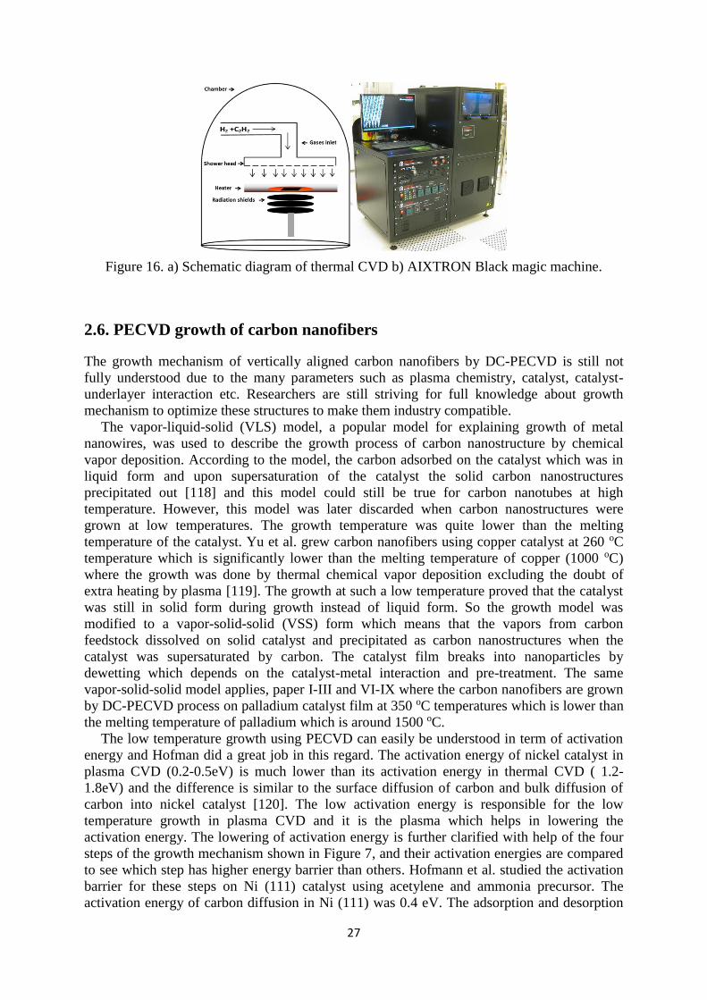
27
Figure 16. a) Schematic diagram of thermal CVD b) AIXTRON Black magic machine.
2.6. PECVD growth of carbon nanofibers
The growth mechanism of vertically aligned carbon nanofibers by DC-PECVD is still not
fully understood due to the many parameters such as plasma chemistry, catalyst, catalyst-
underlayer interaction etc. Researchers are still striving for full knowledge about growth
mechanism to optimize these structures to make them industry compatible.
The vapor-liquid-solid (VLS) model, a popular model for explaining growth of metal
nanowires, was used to describe the growth process of carbon nanostructure by chemical
vapor deposition. According to the model, the carbon adsorbed on the catalyst which was in
liquid form and upon supersaturation of the catalyst the solid carbon nanostructures
precipitated out [118] and this model could still be true for carbon nanotubes at high
temperature. However, this model was later discarded when carbon nanostructures were
grown at low temperatures. The growth temperature was quite lower than the melting
temperature of the catalyst. Yu et al. grew carbon nanofibers using copper catalyst at 260 oC
temperature which is significantly lower than the melting temperature of copper (1000 oC)
where the growth was done by thermal chemical vapor deposition excluding the doubt of
extra heating by plasma [119]. The growth at such a low temperature proved that the catalyst
was still in solid form during growth instead of liquid form. So the growth model was
modified to a vapor-solid-solid (VSS) form which means that the vapors from carbon
feedstock dissolved on solid catalyst and precipitated as carbon nanostructures when the
catalyst was supersaturated by carbon. The catalyst film breaks into nanoparticles by
dewetting which depends on the catalyst-metal interaction and pre-treatment. The same
vapor-solid-solid model applies, paper I-III and VI-IX where the carbon nanofibers are grown
by DC-PECVD process on palladium catalyst film at 350 oC temperatures which is lower than
the melting temperature of palladium which is around 1500 oC.
The low temperature growth using PECVD can easily be understood in term of activation
energy and Hofman did a great job in this regard. The activation energy of nickel catalyst in
plasma CVD (0.2-0.5eV) is much lower than its activation energy in thermal CVD ( 1.2-
1.8eV) and the difference is similar to the surface diffusion of carbon and bulk diffusion of
carbon into nickel catalyst [120]. The low activation energy is responsible for the low
temperature growth in plasma CVD and it is the plasma which helps in lowering the
activation energy. The lowering of activation energy is further clarified with help of the four
steps of the growth mechanism shown in Figure 7, and their activation energies are compared
to see which step has higher energy barrier than others. Hofmann et al. studied the activation
barrier for these steps on Ni (111) catalyst using acetylene and ammonia precursor. The
activation energy of carbon diffusion in Ni (111) was 0.4 eV. The adsorption and desorption

28
energy of acetylene and ammonia in thermal CVD was 0.9 eV and 1.3 eV. So the adsorption
and desorption are rate limiting steps in thermal CVD. These high activation energy barriers
are reduced with the help of plasma so the rate limiting step in PECVD is diffusion of carbon
in catalyst which itself has low activation energy barrier (0.4eV) which justifies the
possibilities of CNFs growth in PECVD at low temperature [121].
There are two type of growth modes of carbon nanotube/nanofiber namely 1) tip growth
and 2) base growth. In tip growth the catalyst particles lies at the tip of the grown carbon
nanostructure where the catalyst lies at the bottom in base growth. It was perceived that the
growth model is controlled by the adhesion force of catalyst particle with the substrate or the
underlayer and this adhesion force is defined by the morphology of the underlayer. The base
growth occurs for the stronger adhesion between catalyst-underlayer and the tip growth
occurs for weak adhesion [122, 123]. If the pore size in the underlayer is comparable to the
catalyst particle size, the particle sticks inside the pore having stronger adhesion force with
the underlayer, resulting in base growth whereas weaker adhesion happens between
underlayer with small pore size and big catalyst particle which result in tip growth carbon
nanotubes [124]. The base growth from smaller particles was also explained such that the
small catalyst particles are chemically more reactive. The carbon diffuses and makes a
hemispherical graphene cap quickly isolating the catalyst surface from further carbon. The
carbon then incorporates from the edges of the catalyst particles. In contrast, for bigger
catalyst particles, the carbon takes a long time for diffusion before making a cap and the
carbon chain diffuses earlier at the metal catalyst interface and lifts the particles resulting in
tip growth [125]. This model is contrary to what Dijon et al. showed on the basis of oxidation
state of iron at the time of growth that the iron is in oxidized state in base growth mode and
iron oxide is more stable than iron itself. However, tip growth occurred from the same size of
un-oxidized catalyst particle in thermal CVD [126]. Tip growth always occurs from thicker
catalyst on metal underlayers in plasma CVD which could be caused by the thermal gradient
between the catalyst particles and substrate. In plasma CVD, the thermal gradient is towards
the catalyst due to plasma heating supporting tip growth whereas in thermal CVD, the
substrate temperature in contact with heater is higher than the top of catalyst particle. The
thermal gradient towards the substrate gives rise to base growth [127, 83]. In addition, plasma
etching keeps the catalyst surface clean for further carbon incorporation from the surface of
the catalyst. Nevertheless, a thick layer of palladium catalyst deposited on the titanium nitride
gives rise to bigger catalyst particles and thus results in tip growth carbon nanofibers as
shown in Figure 17.
Figure 17. Tip growth of carbon nanofibers grown at a) 500 oC and b) 550 oC

29
The mixture of two gases is used to grow carbon nanostructures in which one is the carbon
source gas and other is a carrier gas. The source gases provid carbon feedstock for the growth
whereas the carrier gas is used to etch the amorphous carbon during growth and keep the
catalyst active. Hydrocarbons are mostly used as the carbon source gas because of their
support to grow a wide variety of carbon nanostructures. Methane (CH4) [128, 129, 130],
ethylene (C2H4) [131, 132, 14] Acetylene (C2H2) [133, 83], ethyl-alcohol (C2H5OH) [134]
and carbon monoxide(CO) [135] are most commonly used carbon source gas whereas
hydrogen (H2) and ammonia (NH3), in addition to (nitrogen) N2, Ar (argon) and sometimes
oxygen are used as carrier gas. Depending on the growth requirement different combination
of carbon precursor and carrier gases are used. The mixture of acetylene and ammonia gases
is frequently used in PECVD for the growth of vertically aligned carbon nanofibers [136, 78,
105, 100, 137]. The CN and atomic hydrogen are the active species generated from the gases
in the PECVD process which etches the amorphous carbon from the catalyst to keeps it alive
for carbon diffusion. Atomic hydrogen is generated more effectively from the ammonia than
molecular hydrogen which was proved by the enhancement of growth in atomic hydrogen
when a small amount of ammonia was introduced in CH4/H2 plasma [138]. The acetylene is
the main carbon source for the growth of carbon nanostructure even when growth is
performed using methane because methane decomposes into different other carbon species
during plasma growth and acetylene is one of them. In addition, the acetylene is unsaturated
hydrocarbon which can be decomposed at even lower temperatures [139] and also provide
more ions in the plasma which can help to remove amorphous carbon [140]. Because of these
salient features of acetylene and ammonia, their mixture enables the growth of carbon
nanostructure at such a low temperature (350 oC and 390 oC) described in [paper I-III].
Figure 18. Schematic diagram of DC-PECVD system [145].
The precursors gas ratio, flow, pressure, temperature, plasma current and biasing voltage
are the main parameters for the growth of carbon nanofibers. However random parameter
setting does not grow carbon nanostructures especially at low temperature. Different
ammonia-acetylene gas ratio is used depending on the substrate-catalyst scheme. For the
PECVD case, a higher concentration of ammonia (etching gas) will etch the catalyst or any
grown structure in addition to low growth rate due to low supply of carbon feedstock. Lee et
al. grew using NH3/C2H2 ratio 3, 4, 5 and showed inverse relation of growth rate with

30
ammonia and it was because of the increase in etching species whereas carbon source species
remained the same [141]. Bell et al. showed that 20% of acetylene is the optimum ratio for the
growth. They argued that no extra carbon deposition take place at optimum gas ratio, the
excess gas phase carbon form HCN gas which is pumped out.
The morphology of the carbon nanofibers changed from cone to long conical structures
with higher gas flow and considerable increase in the growth rate of the carbon nanofibers
[142]. The schematic diagram of PECVD growth system is shown in Figure 18.
The pressure plays another role in the growth of carbon nanofiber. At high temperature, the
carbon nanofibers can be grown both at high and moderate low pressure using acetylene and
ammonia gas mixtures. The growth rate has shown to increases with the increase in gas
pressure up to 10 Torr [96]. At high pressure more gas precursors are available for growth.
Higher pressure than 6 Torr is used to grow the carbon nanofibers by PECVD using acetylene
and ammonia gas mixture [143, 144]. Such processes can be made CMOS compatible in
terms of temperature [paper I-III and VI-VIII].

31
3. Characterization of carbon nanostructures based devices
This chapter describes the fabrication and evaluation of the devices based on carbon
nanostructures grown at CMOS compatible temperature. Primarily, small size and fine pitch
bumps of VACNFs, and then their composite with solder and polymer are characterized
electrically and mechanically to show that VACNFs can potentially improve the reliability of
interconnects. Then VACNFs and CNTs are evaluated for supercapacitor applications
including a coin-cell supercapacitor device. Moreover, VACNFs are also evaluated for on-
chip supercapacitors and then on-chip solid-state micro-supercapacitors devices are
demonstrated. On-chip supercapacitors can be the potential sources of energy to power on-
chip micro-devices for IC’s and IoT. Finally parallel plate on-chip integrated capacitors are
characterized.
3.1. Interconnects
3.1.1. Mechanical Characterization
It is important to understand the mechanical properties of the individual CNF and also when
used as turfs for their integration application in the SiP, SoC and chip-stacked packaging. The
general spread in the reported CNF performance [26] is likely ascribed to the different growth
conditions and methods used for the CNFs characterization. Therefore, test structures as close
to real interconnects as possible (grown under the same conditions and on the same
substrates) must be used to gather relevant information and use it input circuit designer.
The mechanical characterizations of VACNFs are performed using different techniques for
different applications. The deflection angle of a single VACNF is found through bending tests
conducted inside an SEM using a nanoprobe. The CNF can be bent upto 70o from its axis and
returned back to initial position elastically [146]. This specific test can be beneficial for
designing nanoelectromechanical systems based applications. In the same work,
nanoindentation and uniaxial compression tests using a flat punch indenter were conducted to
get the axial young’s modulus (~ 816 GP) of a single VACNF grown at 700 oC. Similar axial
Young’s modulus value ~900 GP is obtained for the CNFs film measured by AFM in tapping
mode using a pyramid shaped tip.
Nanoindentation is a non-destructive technique used to characterize the hardness and
modulus taking place at micrometer or nanometer scale. An indentation tip of precise shape is
used with very small load of few milinewton which makes an indent of a small area
comprised of a few square micrometers. A load-depth curve is plotted while moving the tip
down and retracting back and we get the data at run time because of the known geometry of
the indentation tip. This method allows measurement on rough and porous surface. However
it is cumbersome to measure porous materials with other indentation methods where the
indentation tip of unknown area is used, and indentation area is measured using fancy
techniques such as AFM and SEM. Nevertheless, the stiffness is measured from the slope of
the retraction part of the load-depth curve and the elastic modulus is deduced from the
stiffness. Finally the hardness is measured using load per unit indentation area [147]. The
hardness and the Young’s modulus is higher for CNFs grown at low temperature, Table 4
resulting from the higher number of CNFs in contact with the indentation tip due to their
higher density, Figure 19 [148]. The very low values for 550 oC growth might be due to even
lower numbers of CNFs in contact with the indentation tip.

32
Table 4. Mechanical properties of VACNFs turfs grown at different temperatures.
Growth at 390oC Growth at 550oC
Hardness (KPa) 8-8.5 1.8-4.4
Elastic modulus (MPa) 0.84-1 0.26- 0.84
3.1.2. Electrical Characterization and modeling of CNFs resistivity/conductivity
The basic electrical characterization of CNFs turfs is important for the application designing
because the CNFs grown at different conditions have different electrical properties such as
contact resistance between CNFs and substrate, and the resistivity of the CNFs. In [paper I]
the electrical resistivity of CNFs grown at different temperatures, Figure 19, was directly
measured using a card mounted on the system which can give precise control of the vertical
force, thus preventing turfs from damage [149]. The intrinsic resistivity of the CNFs could
then be directly extracted, using the Transmission Line Model of Kelvin measurements of the
CNFs turfs of different height. The conductivity of the low temperature grown single CNF
(6.53x10³ S/m) is 9000 times smaller than that of the copper (5.92×10⁷ S/m) which is the
material currently used in CMOS technology for interconnects. To use for interconnect
purposes, the conductivity of CNFs can be enhanced by coating with metals or making solder
composite which will also enhance the mechanical strength of the interconnects.
Figure 19: CNFs turfs structures grown at a) 550 oC b) 390 oC
In these technique, the electrical resistances of the CNFs are measured in a Kelvin probe
configuration, Figure 20a. The resistance of the turfs increases with the fiber length, showing
uniform behavior of the turf. The total resistance of the CNFs bump is the sum of the
resistance of CNFs turf and their contact resistances both with the substrate and the metal pad,
Figure 20b. The serial combination of the resistances is given as

33
Figure 20. Schematic diagram of a) Kelvin measurement b) Resistances involve in probing of
CNFs [paper I.]
R= RCON1+RCNF +RCON2 (8)
In order to find the contact resistance and resistance of the CNFs turf, the resistances of the
bumps are plotted vs the lengths for CNFs grown at different temperatures as shown in Figure
21. The lower resistance of 550 oC grown CNFs is due to high purity level of CNFs [150].
Figure 21. Measurement of the CNFs turfs [paper I].
A model is made to extract the resistivity of single CNF from the measurement, and the
resistivity is also calculated from the plots using the same assumption as in the model. Finally,
the conductivity of the single CNFs is calculated.
Figure 22. Schematic diagram of a) Transmission line measurement b) CNFs turfs [paper I].

34
Here, the Rs is the resistance per unit length of the CNFs turf and L is the length of the turf
and thus Rs×L is the resistance of CNFs in the turf, Figure 22.
So the above equation becomes
R(L) = RCON1 +RCON2 + Rs×L (9)
The resistance per unit length (Rs) measured as
Rs =resistivity×4
π×Df2 (10)
Where Df is the cross section diameter of all CNFs combined in the turfs, given by
Df = F × D (11)
Each CNF in the turf is considered as a perfect cylinder of diameter 100 nm and all the
CNFs in a turf are resistors of identical resistance lying in parallel format.
Since the growth of the CNFs sparse so the fill factor of CNFs is F in the area of turf of
diameter D. So the number density of CNFs will be
N = F ×(π×D2
4⁄
(π×dcnf)2
4⁄
(12)
N = F ×D2
dcnf2 (13)
The resistivity of the single CNFs:
resistivity_cnf = resistivity × N
=N × Rs × (π ∗ (F × D)2)
4⁄ (14)
𝑐𝑜𝑛𝑑𝑢𝑐𝑡𝑖𝑣𝑖𝑡𝑦_𝑐𝑛𝑓 = 1 ⁄𝑟𝑒𝑠𝑖𝑠𝑡𝑖𝑣𝑖𝑡𝑦_𝑐𝑛𝑓
3.1.3. Wettability by Solder
The low electrical performance of CNFs as found from the previous measurements prevent
them to be used as interconnect pillar autonomously. However, the CNFs composites with
solder or metal are the potential CNFs based solution which can enhance the electrical
performance and mechanical stability of interconnects. To assure reliable composite
formation it is important to find the wettability of the CNFs by the solder where the
wettability determines as how much a molten solder can spread on the CNFs. In fact, the
solder bumps provide both the electrical connection and mechanical support to the chip
assembly, and defines the overall performance of the electronics device. In traditional lead
based solders the wettability was provided by the lead. Today a considerable effort is
conducted worldwide to optimize the properties of lead free solder for interconnect. Different
types of nanoparticles are added to enhance the wettability of the solder. Moser et al. added
small amount of indium into SnAgCu solder and wettability angle decreased from 37o to 22o

35
[151]. The CNTs are already believed to enhance the mechanical strength of the solder by
bridging the brittleness of the solder.
The wettability is tested in different ways and the wetting angle test is quite common in
which the angle between liquid drop and the surface determine the wettability. The lower
wetting angle gives better wettability.
In [paper II], the wettability of CNFs by the solder is demonstrated in two different ways
beside the wetting angle method. In the first method, In290 solder is used to wet the CNFs
where In290 is an alloy of indium and 3% silver. The silver improves strength, and wettability
and low-temperature malleability are similar to the indium. The electrical resistivity, melting
point and tensile strength of the solder are 7.5×10⁻⁶ Ω-cm, 143 oC and 5.5 MPa. A drop of the
solder is applied on the CNFs using drop casting method and analyzed using high resolution
tunneling electron microscope (HRTEM) image, Figure 23. The image clearly shows that
solder has really penetrated inside the CNFs film and filled the space between them. The
absence of voids in between the CNFs-solder proves the good wettability of CNFs.
Figure 23. Cross-sectional TEM image of CNFs wetted in Ind290 solder [paper II].
3.1.4. Electrical performance
The wire bonding packaging was partially eliminated from microelectronics due to the rise in
the density of I/O interconnect, and taken over by the flip chip which started from the C4
(controlled collapse chip connection) solder bump technology by IBM. The flip chip technol-
ogy is keeping the pace with small size and fine pitch I/O’s density however by using the dif-
ferent materials for the bumps. The solder balls face limitation at low dimension such as fa-
tigue and creep caused by thermo-mechanical stress in solder joint due to CTE difference of
the materials, EM failure and IMC formation [152]. The solder bump was replaced by the
copper pillar technology where the pillars contain solder cap to make joint with the pad. Am-
kor introduced 40 µm copper pillar with 80 µm pitch in 45 nm node application processor
where the caps were made of SaAg solder [153]. However, IMC formation and EM are still

36
the main limitation of the copper pillars [8], in addition to bridging of the neighboring copper
pillars due to spreading of the solder [154].
To present carbon nanostructure as a reliable solution of current and future interconnect
challenges the electrical properties of these materials are measured in different ways. Chen at
al. measured by bonding two transferred CNFs pads on two different solder coated substrate
and achieved 360 mΩ bump resistance [155].
To assess the electrical performance of the CNF-metal composite for interconnect kelvin
probe measurements or daisy chains [156] are the method of choice. Yet for technological
proof of concept relative measurements [paper II] can be well illustrative, less time consum-
ing and much more economical to perform. In [paper II], CNFs/solder composite joints were
realized with the use of a flash gold layer and standard thermal compression assembly tech-
nique. The 2-probe I-V curves and extracted resistance curve for bare metal and metal coated
CNFs samples are shown in Figure 24a and b. The CNFs/solder composite-bumps intercon-
nect show similar linear current-voltage behavior as a bare metal contact and have almost
similar electrical resistance. The resistance of metal coated CNFs is higher which could be
due to poor gold coating of CNFs. Similarly electrical performance of fine pitch CNFs bump
proposed in paper I can also be improved by selective electroplating.
Figure 24. Electrical characteristics of solder bumps on Gold coated a) silicon chip b) CNFs
chip. [Paper II]

37
3.1.5. Bonding performance
Along with good electrical contact between chip and substrate, good mechanical strength is
also important. The solders provide the good mechanical strength in solder based intercon-
nects, and in ACF based interconnect the mechanical strength is provided by the paste. The
mechanical strength of the bonded chips is measured by measuring shearing strength which is
conducted by applying a force using stylus [155].
Low temperature polymer could be advantageously used as adhesive for bonding [paper
II]. The VACNFs are grown on three silicon carbide (SiC) power transistor chips and polymer
is spin coated on to make a CNFs-polymer. The chips are bonded on three different types of
readout chips as shown in Figure 25 [paper II].
A commercial lead frame substrate with 1.45x1.45 mm2 CNFs chip bonded on it is pasted
on a piece of metallic block using strong adhesive and the whole assembly is placed on the
digital weight machine used in kitchen. A piece of hard plastic wedge is attached with the
cylinder to apply force above on the bonded chip. The force applied by the pump is read from
the weight machine. The average force was 2300 g (10 MPa) which qualify the assembly as
MIL X1 standard of microelectronics. The electrical measurement conducted on silicon
substrate [paper II] shows linear I-V curve with good Ohmic contact.
Figure 25. a) SiC power transistor with CNFs bonded on a Silicon substrate b) Si-CNFs chip
bonded with commercial lead frame c) SiC bonded with DCB substrate [Paper II].

38
3.2. Electrochemical Characterization of supercapacitor
The combination of different electrochemical characterization techniques are used to assess
performance of the supercapacitor such as cyclic voltammetry (CV), galvanostatic
charge/discharge (GCD) and electrochemical impedance spectroscopy techniques (EIS).
Moreover, to assess the performance of the electrode material only or as the complete cell
three electrode or three electrode measurement setups are used. This session deals with the
different characterization techniques and measurement setups and finally describes the per-
formance of the carbon nanostructured based electrode materials presented in [paper IV-VII].
3.2.1. Cyclic Voltammetry
Cyclic voltammetry is widely used to characterize electrode materials. The potential applied
to the electrode is scanned between two voltage limits with linear scan rate and the current is
measured. The voltage scan reverses direction on reaching the voltage limit to complete cycle.
The current at the electrode is plotted vs applied voltage which results in cyclic
voltammogram (CV). The CV curve of an ideal EDLC electrode is rectangular as shown in
Figure 26, where the current changes sign immediately when the direction of the voltage scan
rate is reversed. The capacitance of an ideal supercapacitor can be measured using equation
(15). However, many non-ideal elements such as pseudocapacitance, electrolyte degradation
and rate limitation are involved in the supercapacitor, therefore a real voltammogram usually
deviates from rectangular CV shape, as shown in Figure 26. The pseudocapacitance
represented by peaks in the blue CV curve originates from the redox reaction taking place at
the surface of the electrodes. The electrolyte degradation happens when the voltage range
exceeds the stable voltage window of the electrolyte. The faradaic reaction occurs due to the
degradation of electrolyte resulting in higher current shown by the peaks at the extreme
voltages in the CV. Finally the rate limitation comes from the slower response due to the
different resistances involve in the system.
𝐂 =𝐢
𝐬 (15)
Where s is the voltage scan rate
Figure 26. CV curve of ideal EDLC and the effect of redox reaction on ideal capacitor.

39
Therefor the specific capacitance is measured by integrating the charge or discharge curve
of CV divided by the voltage using equation (16)
Csp=∫ idV
ms(V2-V1) (16)
Where s is the voltage scan rate, V2-V1 is the voltage scan range in the CV, i is the current and
m is the mass of the electrode (can be area if areal capacitance is required).
Because of the redox reaction the charge and discharge curve are not symmetric and the
capacitance is, therefore measured as average of charge and discharge curves. In [paper IV-
VIII] cyclic voltammetry is used for capacitance measurement.
3.2.2. Galvanostatic Charge/Discharge
The galvanostatic charge/discharge (GCD) is another technique for characterization and give
additional information about the supercapacitor behavior. In GCD the charging and discharg-
ing is performed using controlled current and voltage vs time is monitored, Figure 27 unlike
CV where the controlled voltage is used for charging/discharging. The GCD is mostly used to
measure the capacitance, cycle life of the supercapacitor and the IR drop. The IR drop is volt-
age drop due to the internal resistance at the beginning of the discharge represented by the
vertical line in the discharge curve, Figure 27. The internal resistance also called equivalent
series resistance (ESR) can be calculated from equation (17).
Figure 27. Voltage Vs time curve at constant charging/discharging current
ESR =ΔVdrop
ΔI(Ω) (17)
where ΔI is the difference between charging (I1) and discharging (I2) currents when the direc-
tion of the current is changed for discharging and given by |I1-I2|.

40
The capacitance is measured from the discharge curve using equation (18). The charge and
discharge curves are linear and symmetrical at various current for an ideal capacitor [157].
C = Idt
dV(F) (18)
Where I is constant discharge current (A), dV/dt is the slop of the discharge curve after ΔIR
drop.
Cyclic charge discharge techniques is used to measure the cycle life in which the superca-
pacitor is charged and discharged to specific number of cycles and the capacitance retention
after last cycle gives the cycle life.
3.2.3. Electrochemical Impedance Spectroscopy (EIS)
EIS is the characterization techniques which gives detailed information about the behavior at
the electrode/electrolyte interface and also give other frequency dependent resistances in addi-
tion to Ohmic resistance or ESR.
In this technique, the system is perturbed using a small sinusoidal potential, applied in the
frequency range 10 mHz- 1 MHz. The ratio of corresponding sinusoidal current and voltage
signal give the complex impedance for a particular frequency. In a capacitor, the current lags
the voltage by an angle (ϕ), and the ϕ is 90o for an ideal capacitor so if the applied voltage is
V(ω)= Voexp(jωt) (V) (19)
The current will be
I(ω)=Ioexpj(ωt+ϕ) (A) (20)
Where the Vo and Io are the maximum amplitude of voltage and current signal.
The electrochemical impedance will be
Z(ω) =V(ω)
I(ω)=
Vo
Ioexp(−jϕ)(Ω) (21)
The complex impedance can be represented as
Z(ω) = ZRe + jZIm (22)
Where ZRe and ZIm are the real and imaginary parts of the impedance, respectively.
The impedance modulus is
|Z(ω)| = √ZRe2 + ZIm
2 (Ω) (23)
The phase angle is
ϕ = arctan (ZIm
ZRe)(o) (24)

41
Two types of plots are derived from the EIS data for analysis of supercapacitor: the
Nyquist plot and Bode plot. In a Nyquist plot, the imaginary part of impedance is plotted ver-
sus the real part of the impedance. The Nyquist plot of an ideal EDLC will be a vertical line
containing only the double layer capacitance, Figure 28a. However, the plot contains three
parts, an intercept at x-axis at high frequency (Rs), a semi-circle loop (Rct), a linear (War-
burg) region (Rw) and a vertical line in low frequency region, Figure 28b. The Rs represents
the real impedance (Ohmic resistance), which is the sum of the current collector and bulk
electrolyte resistances. The diameter of semi-circle represents interfacial charge transfer re-
sistance [158]. The Rw region is the straight line at 45o representing diffusion resistance,
which arises at high frequency due to the lower time available for ions to diffuse inside the
small pores of the electrodes. The vertical line represents the dominant capacitive behavior by
the formation of electrical double layer [159]. However, the Nyquist plot does not give the
frequency of particular point on the plot. By considering the capacitance and resistances, the
basic equivalent circuit model of a supercapacitor thus becomes, Figure 28b.
Figure 28. a) Nyquist plot of EDLC a) Ideal b) Ordinary c) Basic equivalent circuit of EDLC.
The Bode plot gives the information about the frequency behavior of the supercapacitor. In
such a plot, the modulus of the impedance and its phase angle are plotted vs the frequency. A
-90o phase angle represents the ideal capacitive behavior of the supercapacitor at particular
frequency or frequency range. However in real supercapacitors the phase angle does not reach
-90o and stays between minus 80-84o mainly due to the Rs of the system [160]. The frequen-
cy, for which the phase angle reaches -45o (i.e. equal capacitive and resistive contribution)
called the characteristic frequency (fo) and it is used as a figure of merit of a supercapacitor
for comparison purpose. At frequencies above fo the resistive behavior of the impedance dom-
inates whereas below fo the capacitive behavior of the impedance dominates. The time con-
stant defined as1/fo, is the minimum time required to discharge the capacitor with more than
50% efficiency [161]. The characteristic frequency activated carbon is usually close to 1 Hz
[162] and efforts are made to increase fo for high frequency application, the fo of value 3579
Hz is shown for graphene based micro-supercapacitor with corresponding time constant of
0.28 ms [161].
3.2.4. Measurement Setups
There are two type of measurement setup, one with two and the other with three electrodes. In
three electrodes setup the electrode materials are characterized against the electrochemical
stable electrodes called reference electrode and counter electrode. The potential of the elec-
trode material is measured accurately relative to a reference electrode where the reference
electrode has a known redox potential. The current against counter electrode is monitored to

42
assess the electrode/electrolyte behavior. In this way, the fundamental properties of the elec-
trode material can be monitored. It gives the capacitance of the single electrode and therefore
it is also called half-cell measurement.
In two electrodes setup both electrodes contain materials for energy storage and are sepa-
rated by semi-permeable membrane which prevents electrodes from short circuiting and al-
lows only the ions to pass. This is used to measure the full device and therefore the meas-
urements are called full-cell measurement. The electrodes in the cell are typically symmetric
to get maximum capacitance and by this the capacitance of the one electrode can be estimat-
ed.
In fact there is a double layer charging on both sides of two identical double layer capacitors
are connected in series in a complete symmetric supercapacitor and the capacitance of the
single electrode can be calculated as
1
Ctotal=
1
C1+
1
C1
where Ctotal and C1 are the total capacitance and capacitance of single electrode of the super-
capacitor
C1 = 2Ctotal
For gravimetric specific capacitance of single electrode Csp, the equation will become
CSp =4Ctotal
m
where m is the total mass of the electrode material inside the supercapacitor.
3.2.5. Electrode materials
As indicated in the precedent sections, the performance of the supercapacitor can be enhanced
by increasing the specific surface area and the conductivity of the electrode materials and car-
bon nanomaterials such as carbon nanotube, carbon nanofiber and graphene are investigated
extensively because of their high conductivity, chemical stability and high surface area. The
theoretical surface area of graphene and open tips CNTs is around 2200-2600 m2/g and the
corresponding specific capacitance of graphene is 550 F/g. Several composite materials made
of different carbon nanomaterials have also been successfully demonstrated as electrode for
supercapacitors using different plasma treatments for their functionalization [paper IV]. An
oxygen plasma treatment was performed to open the tips and to functionalize CNTs, the spe-
cific capacitance value of 440 F/g are obtained from CNTs [paper IV]. Similarly, by oxygen
plasma treatment of electrospun CNFs the specific capacitance of 377 F/g is obtained. The
carbon nanomaterials composites are also made and binder are usually used to make compo-
site which add the dead mass to the electrode materials and also closing the pores. The com-
posites are also made without binder, and in this case the carbon nanomaterials are embedded
inside electrospun CNFs by electrospinning along with. The CVD grown CNTs were electro-
spun with polyacrylonitrile to make CNFs and CNTs composite resulting in high specific ca-
pacitance of 417 F/g and higher overall conductivity of composite. The conductivity of PAN-
CNFs was 0.86 S cm-1 and increased to 8.82 S cm-1 on making composite with CNTs.
In paper V, the carbon nanomaterials composites are made by directly growing VACNTs
on electrospun CNFs. The direct growth provides the metallic contact between of CNTs and
electrospun CNFs which could potentially reduce the Ohmic resistance of the electrode mate-

43
rial. The fabrication of the CNTs is a quick and cost effective two steps process described in
detail in the paper V. Tunneling electron microscopy (TEM) is conducted for detailed charac-
terization and described in the paper, Figure 29a. The CNTs are multiwalled and number of
walls varies between 3 and 8, Figure 29b. The catalyst particles exist inside the CNTs and
located at the tip on most of them. The capacitance from the composite was low around 20
F/g which might be due to electrolyte-phobicity of the composite materials. The composited
was treated with the mixture of nitric and sulfuric acid to etch the catalyst particle. The treat-
ment opens the tips of CNTs providing more surface area and also turned the composite into
electrolye-philic by introducing oxygen groups on the CNTs.
Figure 29. TEM images of CNTs grown on CNFs a) CNTs b) walls of CNTs [paper V].
The electrical conductivity of composite is 15 times better than only CNFs, and the surface
area and thus the specific capacitance improve 3 times and 2 times [paper V]. The energy
density and power density of composite materials is also high. The energy density is close to
highest predicted value of the supercapacitor as shown in Ragone plot, Figure 12.
The generation of 3D electrodes can advantageously be generated by depositing catalyst in
liquid form and, catalyst nanoparticles are usually dispersed in liquid polymer for this pur-
pose. In [paper VII], the catalyst is deposited in nanoparticles form using different polymer-
Pd nanoparticle solutions. The size of the nanoparticles is in the range of 2.3 to 8.8 nm. The
deposition is performed by spin coating which is quick and low cost method, and does not
need expansive cleanroom environment.
The properties of the CNFs grown using nanoparticles and metal catalyst have been shown
to be as suitable as the one grown from metal films for supercapacitor applications using cy-
clic voltammetry. The cyclic voltammograms (CV) curve of both types of CNFs are fairly
rectangular showing the good EDLC behavior, Figure 30. However, CV curves of nanoparti-
cles grown CNFs show more rate limited behavior which might be due to more resistive con-
tact between CNFs and underlayer.

44
Figure 30 Cyclic voltammograms of CNFs grown at a) different temperatures using Pd film.
b) 550 oC using different concentrations of Pd nanoparticles [Paper VI and VII].
The areal specific capacitance (per foot print area) proposed on-chip supercapacitors based
on VANCFs grown at different temperatures are shown Table 5 and Table 6. The higher
capacitance of CNFs grown at high temperature and with high concentration of Pd catalyst is
due to the higher surface area by the longer and denser CNFs. The cyclability test showed that
the CNFs retained 80% of its capacitance even after 1000 cycles.
Table 5. Properties of CNFs grown at different temperatures using thin film catalyst and
specific capacitance pF µm-2 (footprint area) at different scan rates [Paper VI]. Growth
Temperature
( oC)
Length
(µm)
Diameter
( nm)
Capacitance
(mF)
at 10 mV/s
Specific.
Capacitance
(pF/µm2)
Csp (pF/µm2)
at 50 mV/s
Csp (pF/µm2)
at 100 mV/s
Bare chip 0,01
390 3 88 4 55 35 29
450 5 21 5 63 35 27 500 8 30 5,5 70 46 39
550 20 47 6,4 82 51 40
Table 6. Properties of CNFs grown using different concentrations of Pd nanoparticles and
specific capacitance mF cm-2 (footprint area) at 10 mV s-1 scan rate. [Paper VII] PVP:Pd Growth temperature
(oC)
Weight ( g) Length (µm) Specific Capacitance
(mF cm-2)
38:1 550 0.0000528 14 1.001
18:1 550 0.0002448 9 3.915
9:1 550 0.000916 5 9.014
The specific capacitance is higher than silicon trench base on-chip solid state capacitance
offered by IPDiA [10] but the response is slower due to lower mobility of ions of the electro-
lyte and also does corrosion of the metal. Moreover the encapsulation of aqueous electrolyte
base supercapacitor is a challenge because the leakage of the electrolyte will create short cir-
cuit between other devices on the chips and also destroy them by chemical reaction. Yet, the
encapsulation limitation excludes the possibility to build aqueous electrolyte based superca-
pacitor directly on the on the CMOS chip.

45
3.2.6. Coin-cell supercapacitor
Supercapacitors can provide high power density but low energy density as shown in Ragone
plot, Figure 12, and substantial research is currently performed to enhance the energy density.
The low energy density of current supercapacitors prevents them to be an independent energy
storage device. Nevertheless they can be used in parallel with the battery to provide peak
power and can be charge via ordinary power of the battery. In this way, the life of the battery
can be enhanced. The coin-cell is the industrial adopted energy storage packaging and hence
by replacing battery material with the carbon nanomaterials the coin-cell supercapacitor can
be made [163].
Supercapacitors packaged as a coin-cell was demonstrated [paper IX] made of activated
non-stacked reduce graphene oxide applied on aluminum current collector using a binder as
electrode material and 1 M TEABF4 as an electrolyte. The capacitance of coin-cell was 147
mF however the sum of Ohmic and charge transfer resistance was high (15 Ω) [164]. The
composited of activated carbon, carbon black (acetylene black), graphite, and poly(vinylidene
fluoride-co- hexafluoropropylene) were used as electrode material and [BMIM+][BF4-] as
electrolyte to make coin-cell supercapacitor giving high areal capacitance value 45 µF/cm2
however the ESR was around 1 kΩ [165]. The Graphene nanosheet were also grown directly
on current collect at 1000 oC and the volumetric capacitance of values were 53 F/cm-3 and 50
F/cm-3, in 6 M KOH and 1 M TEABF4/AN electrolyte respectively [166].
An approach to integrated CNFs Ifor enhanced performance of supercapacitor packed as
coin-cell is presented in [paper IX], the VACNFs based coin-cell supercapacitor were made
in which CNFs grown directly on current collector using DC-PECVD process are used as
electrode materials and ion liquid as electrolyte. The CNFs growth process was done in two
steps such deposition of catalyst and growth of CNFs which does not involve any binder and
complex chemical processing. Finally the assembly of coin-cell was performed in standard
way as shown in the Figure 31a, and the complete coin-cell device is shown in Figure 31b.
The catalyst to grow CNFs was deposited by spin coating method [paper VII] which is quick
and low cost deposition method thus making the entire process industrially applicable.
Figure 31. a) Assembly of coin-cell b) Coin-cell device [paper IX].
The capacitance of the coin-cell supercapacitor is 5.6 mF which 17 times more than the
capacitance of the coin-cell without CNFs showing the considerable contribution of the CNFs
in energy storage. In addition, the fabrication process is economically favorable and quick.
The ESR value was very low below 2 Ω due to direct growth of CNFs providing metallic
contact with current collector. The power density values of up to 1 W/cm2 can be realized
which have potentially application in electronics which will be discussed in next chapter.

46
3.3. On-Chip capacitor
To comply with miniaturization and high performance demand from electronic devices more
devices are packed on small area which also leads to have more efficient energy storage on
the chip. The energy sources can be used to compensate the energy turbulence from the
existing power source or can independently be used to power up the on-chip devices. This
section deals with the fabrication and characterization of two types of passive on-chip
integrated energy storage components based on VACNFs; a 3D solid state parallel plate
capacitor and an interdigitated supercapacitor based on Sol-gel electrolyte. These capacitors
can be used as decoupling capacitor and RF filter. The particular voltage or capacitance can
be tuned by connecting these capacitors in parallel or series format.
The future compact and smart electronic devices trend is challenging for semiconductor
industry and the industry is handling these challenges in two different ways by enhancing the
performance of the CMOS chip and by efficient packaging. The performance of the CMOS
chip is enhance by increasing the density of active devices as predicted in the Moore’s law
and by replacing on-chip discrete component with more efficient ones. The packaging is en-
hanced by using system on Package (SIP), package on package (POP) technique and finally
moving to 2.5D and 3D packaging technology by introducing silicon interposer and through
silicon via (TSV) technology. The passive capacitors with high specific capacitances are re-
quired in the closed vicinity to efficiently power up devices on the chip by keeping the pack-
age as small as possible. For this purpose the capacitor are built on the CMOS or on the inter-
poser close to the chip. The supercapacitors are the best candidate to get high specific capaci-
tance as shown in Ragone plot which require high surface area of the electrode. Different car-
bon nanomaterials based flexible and on-chip micro-supercapacitors are already proposed in
which the electrode materials are deposited using electrodeposition, 3D printing requiring
long fabrication procedure. The CMOS compatible process fabrication is required to make
supercapacitor directly on the chip.
3.3.1. Full solid-state capacitor
On-chip capacitors are both mounted in the closed vicinity of the CMOS chip as a discrete
component and integrated directly on the CMOS chip. The integration on CMOS chip helps to
avoid the long current path and thus lower impedance at high frequency. High areal specific
capacitance (per foot print area) is desirable from a capacitor for its better performance for
decoupling purposes. Different types of decoupling capacitor used for 65nm CMOS technolo-
gy are shown in the Table 7, where the MOS capacitors are made using transistors fabrication
steps.
The capacitors have low areal specific capacitance and their fabrication involve extra pro-
cessing steps. Recently, high capacitance integratable planer and 3D capacitors are commer-
cialized by different companies. IPDiA (now muRata) and Franhaufer made the capacitors of
capacitance 0.81-1 pF/µm2 in 3D configuration with profile of thickness 100-150 µm. How-
ever the capacitors are fabricated by making deep trenches in the silicon which is an expen-
sive and not optimal for serial integration.
In the approach used in [paper III], VACNFs based solid state capacitors intended to inte-
grate on CMOS chip are fabricated using CMOS compatible processes, [paper III]. The
VACNFs providing high surface area are grown directly on silicon substrate, Figure 32a, and
then conformal coated by very thin layer of dielectric, and both parameter guarantee high spe-
cific capacitance. The dielectric can be deposited using different techniques such as LPCVD,
PECVD and ALD. The CVD techniques are limited in performance due to low quality of step
coverage and control on the film thickness but ALD due to sequential and self-limiting sur-

47
face reaction characteristics have better control on film thickness and single molecular layer
deposition capability provides better conformal coating of nanostructures, Figure 32b.
Table 7: Integrated decap [167]
Decap Unit L
( µm)
Unit W
( µm)
Area
( µm2)
Layout- extracted
Ceff (fF)
Specific caitance
fF/ µm2
nMOS 1 0.83 55 500 9.1
nMOS_25 1 2.29 135 500 3.7
nMOS_LVT 1 0.82 55 501 9.1
A_nMOS 1 0.80 61 498 8.2
pMOS 1 0.91 61 501 8.2
CMOS 1 0.42 75 493 6.6
1 0.42
MIM 2.01 2.01 1343 507 0.4
GATED 1 1 73 500 6.8
0.06 0.06
B2N 1 1 75 500 6.7
1 1
MOM_M1 6.7 0.09 1201 507 0.4
Figure 32. a) VACNFs b) Conformal coating by aluminum oxide dielectric [paper III].
The areal capacitance of about 10-15 nF/mm2, have been demonstrated for low profile de-
vices, about 10 µm in height, Figure 33a. Therefore such capacitors can easily be integrated
on chip-chip, chip- die and even in between multi die- stack packaging.
A model is also made in the paper III to estimate the area of the VACNFs contributing for
the capacitance. The CNFs are assumed as solid cylinders of same diameter and divided into
length categories. The total surface area of the CNFs and finally total theoretical capacitance
is calculated. From the difference between theoretical and measured capacitance the surface
area of CNFs contributing to capacitance is almost 71% of the theoretical surface area. The
low areal contribution from CNFs is due to deposition of top metal by sputtering method
which does not do the conformal coating of CNFs and it is confirmed by the protruded layer
of top metal above the ALD coated CNFs, Figure 33b.
48
Figure 33. SEM picture of the a) Capacitor b) Top electrode [paper III].
3.3.2. On-chip microsupercapacitor
The gel electrolytes are the strong candidate to provide the packaging challenges faced by
liquid electrolyte and are investigated extensively for flexible electronics. The gel electrolyte
turn into solid on drying therefore are also called solid state electrolyte. The gel electrolyte
performs two tasks; first it works as electrolyte and second it provides the encapsulation to the
device potentially eliminating the additional packaging step. The gel electrolytes are
composed of polymer gel and aqueous electrolytes and contained 70% of aqueous electrolyte.
Recently H2SO4/poly (vinyl alcohol) (PVA) bases gel electrolyte are show for flexible
electronic on polydimethylsiloxane (PDMS) elastomer [168]. KOH/PVA was also used, and
KI was added to introduce psuedocapacitance and to enhance conductivity of electrolyte
[169]. However, aqueous electrolyte based gel electrolytes have low voltage window due to
low ionization voltage of water. The ionic liquid based gel electrolyte are also explored due to
wider voltage window and therefore called Ionogel. The [EMIM][NTf2]and silica gel based
gel electrolyte are used for flexible electronic providing the voltage window of 3V [170].
In paper VIII, VACNFs based interdigitated on-chip micro-supercapacitors are made in
which polymer gel based electrolyte is used. The VACNFs are directly grown on the digits of
the interdigitated supercapacitor and gel electrolyte is deposited using simple drop casting
method. The wettability by electrolyte, Figure 34, in addition to extraordinary electrical,
mechanical and high surface area properties, is an important aspect to utilize the high surface
area for energy storage. The electrolyte-phobicity prevents the electrolyte to penetrate inside
the pores of the electrode materials. The wettability can be enhanced by introducing some
surface functional group which will help the adsorption of electrolyte ion on the surface of
electrodes. The functional group might add some faradaic redox reactions potentially resulting
in 5-10% increase in total capacitance [171]. The functional group can be introduced by wet
and dry treatment of carbon nanostructures [172]. In [paper VIII], VACNFs are functionalized
using oxygen plasma treatment also ensuring in wetting by the electrolyte.

49
Figure 34: a) Electrolyte drop on CNFs before plasma treatment b) CNFs wetting by
electrolyte after plasma treatment.
Like an ordinary battery, the supercapacitors also have freedom in designing for bulk
energy storage application but designing options are limited for on-chip energy storage
application. The on-chip supercapacitor should be efficient in energy storage and release, and
should be low profile. Interdigitated design is used here in which oppositely charged
electrodes are placed next to each other at certain gap. This design does not require any
separator thus providing low profile and the freedom to vary the gap between the digits. The
supercapacitors of this design could comply with different types of packaging especially
limited gap stacked-die packaging.
The dimensions of the digit are kept same (3694 µm × 94 µm) but the gaps between the
digits is 10, 20, 30, 50 and 100 µm however gap size is same between the digits in a micro-
supercapacitor as shown in schematic diagram and SEM image of VACNFs, Figure 35.
Figure 35: a) Schematic diagram of interdigitated pattern b) CNFs on the digits.
The CV curves of interdigitated capacitor made using VACNFs grown at different
temperature are fairly rectangular showing the EDLC behavior, Figure 36. The electrode area
increases with the decrease in gap between the fingers and the corresponding capacitance also
increases, Figure 37. The capacitance retention of 75-82% at higher scan rates is obtained for
390 oC grown samples providing the high rate capability which might be due to low contact
resistance of CNFs with current collector as measured in [paper I] and further confirmed by
the Nyquist plot given in [paper VIII]. Nevertheless maximum areal specific capacitance of
the value 1 mF/cm2 is obtained.

50
Figure 36. CV of CNFs grown at a) 390 oC b) 550 oC
Figure 37. Capacitance retention at different scan rates for CNFs grown at a) 390 oC b) 550 oC
[paper VIII]

51
3.3.3. Modeling of on-chip microcapacitor
The frequency at 45o phase angle represents characteristic frequency (fo) and the
corresponding time constant (τo= 1/ fo) defined as the minimum time required to discharge the
capacitor with more than 50% efficiency [161]. For high frequency application, the response
time should be small (high characteristic frequency). The characteristic frequency at particular
phase angle is inversely related to the real impedance of the supercapacitor which comes from
the current collector, electrodes and electrolyte resistances.
A model to extract the intrinsic performance of the interdigitated supercapacitors and study
the contribution and hence limitations in the design by reducing the real impedance the
characteristic frequency can be increased [paper VIII]. The equivalent circuit shown in Figure
38, can be numerically analyzed using RF simulator such as keysight ADS. In the circuit, the
resistance value R2 between each digit on the connecting line is assumed same because of the
same gap size. The resistance between probing pad and first digit is R3, and finally the
resistance of each digit is named R1 because of the same dimension of the digits. The
capacitance C1 between the digits is also considered same. The device performance is shown
to be mainly limited by the serial resistance of the fingers. Minimizing this resistance could
increase remarkably the characteristic frequency to 965 Hz and 866 Hz for 390 oC and 550 oC
grown interdigitated micro-supercapacitors and times constant is about 1 ms.
Figure 38. Equivalent circuit of interdigitated capacitor [paper VIII].

52

53
4. Applications of carbon nanostructures
4.1. Electrical component packaging
4.1.1. Solder-based Alternate ACF
Anisotropic conducting film (CNFs) is a technology used for bonding chip to substrate for
interconnection. The conventional ACF is an adhesive polymer matrix with conductive
particles embedded and usually found in the form of tape or paste [173]. The conducting
particles are found in different forms such as pure metal, solder and metal coated polymer
balls. The tape is sandwiched between chip and substrate and the contact is made by thermal
compression bonding as show in the schematic diagram, Figure 39a. Because of the simple,
low temperature and cost effective nature of the ACF assembly process, it has been used for
interconnection in technologies requiring low temperature bonding such as chip-on-glass
(COG), flex-on-glass (FOG), flex-on-board (FOB), flex on flex (FOF), chip-on-flex (COF)
and chip-on-board (COB) due to their fine pitch capability [174], but still have few
limitations.
In metal ball ACFs, each bump has a certain density of metal balls to make the low
resistive contact between the bump and pad. Upon misalignment, the density of metal balls
could potential decreases as shown in the schematic diagram, Figure 39b, resulting in high
contact resistance. The metal ball density can be increased by increasing the amount of metal
balls in the solder but high metal balls density enhances the probability of short circuiting
between the adjacent bumps, Figure 39c [175].
Figure 39. a) ACF with solder ball embedded. b) Misaligned bumps creating high resistance
c ) Short ciruit by solder ball in ACF membrane . d) Short ciruit by solder ball in the paste.
The paste based ACF consists of metal and insulating layer coated polymer balls making
them insulating in x, y and z directions. The balls between the bumps burst on compression
creating a metallic contact [176] and the rest of the balls behave as insulator due to insulating
layer on it. However, the metallic ball could create short circuit between metal and substrate

54
bumps when compressed as shown in Figure 39d. Different materials, other than spherical
balls and paste, are investigated to enhance the metallic contact between bumps and to reduce
the movement of the spherical balls during pressing. Diop et al. made ACF based on vertical
Ni fibers instead of spherical metallic balls and got 418 mΩ contact resistance for a 370 µm
radius bump [177]. An ACF with embedded metal particles in electrospun nanofibers were
investigated nowadays. Suk et al. embedded Sn3.0Ag0.5Cu solder and Ni/Au-coated polymer
in nanofibers by electrospinning Nylon 6 which suppress the movement of the balls during
resin flow. The contact resistance of solder bump of size of 13 x80 µm was 4.6 mΩ [178].
Similarly, Lee et al embedded insulated conductive particles in PVDF nanofibers and the con-
tact resistance was 500 mΩ for 12x12 µm pads [179]. Moreover, Tao et al. made polymide
ACF containing with Cu nanowire [180].
In another approach [paper I and II], VACNFs grown directly on metal pad using CMOS
compatible process could provide an alternate for the problem faced by ACF. VACNFs are
bonded to solder while rooted on the IC pads making composite materials. The solder-CNFs
matrix, studied using TEM, Figure 40a, show that the CNFs trees can extend above the inter-
metallic solder region.
The solder-CNFs composite could make the metallic contact between the pad and bump,
and the compressive strength of the VACNFs would guarantee the significant reinforcement
of the solder bump, in addition to preventing the deformation and slipping out of the solder
from the pad, Figure 40b.
Figure 40. a) State of the art image [145] b) Schematic diagram, of solder-CNFs matric bump.
Embedding VACNFs into polymer [paper II] could also provide a type of ACF film, with
dual purpose. Primarily, it removes risk for lateral conduction and removes the need of align-
ment [181]. Secondly, CNFs- polymer can be used for flip-chip bonding when the soldering is
not possible due to non-solder friendly surface or the surface which cannot bear high solder-
ing temperature. The interconnects made by bonding polymer coated CNFs and copper pillar
are shown in the Figure 41. The copper pillars are attached to the CNFs tip and no connection
exists in lateral direction.

55
Figure 41. The bonding of polymer coated CNFs with copper pillars.
4.1.2. Decoupling and energy storage
The numbers of active devices on the CMOS chip are increasing due to on-going miniaturiza-
tion of features (transistors) and the switching frequency of these devices is also increasing.
The simultaneous switching of the active devices at high frequency draws larger current at
high frequency which is difficult to handle for the power supply resulting in delay of power or
power supply fluctuations. Moreover, there also exists impedance in the current path connect-
ing power supply and current load due to the Ohmic resistance of the metal and, the induct-
ance because of the change in current at high frequency, Figure 42a. The impedance per unit
length of the current path is given by the equation
Zsp(ω)=r+jωl
Total impedance= Z(ω)=Zsp(ω)×d
Where r and l are resistance and inductance per unit length of the current path respectively.
The combined effect of power supply delay and extra impedance on the current path results
in a voltage drop (fluctuation) at the current load. The performance of active devices is then
compromised if the voltage of power supply drops below from certain threshold. The decou-
pling capacitors are used to suppress the voltage drop at the current load by releasing charge
when the voltage at current load drop below tolerable level and get charged during the interval
when the power is drawn from power supply, Figure 42b.
Figure 42.a) Impedance of the current path b) Capacitor location from source and current
load.

56
The location of the decoupling capacitor both at power supply and load resistance plays a
critical role for efficient performance, since the decoupling capacitors should provide the
charge to current load and also get charged during relaxation time when the power is drawn
from power supply to provide the charge during next switching. Therefore, for best perfor-
mance the decoupling capacitors should be located closed to the switching circuit within a
radius called maximum effective radius. Beyond this radius the decoupling capacitor is not
effective due to high resistance and inductance and this radius is decreasing for each new
technological node, Figure 43 . The target impedance, the maximum impedance of the current
path, which give a power ripple lower than the tolerable level of the power distribution net-
work is first calculated using the equation (25)
Ztarget =Vdd×ripple
I(Ω) (25)
Where Vdd is power supply voltage, ripple is the percentage of the Vdd considered as noise, I
is current.
By using the equation the maximum effective radii is calculated by equation (26)
dmax =Ztarget
Zsp=
Vdd×ripple
I×√r2+ω2l2 (26)
Where √r2 + ω2l2 is magnitude of the impedance of unit current path [182].
Figure 43. Projection of the maximum effective radius as determined by the target impedance
for future technology generations: Imax = 10mA, Vdd = 1V, and Ripple = 0.1V [182].
The passive MLCC (multilayer ceramic capacitor) capacitor are mounted using surface
mount technology on the package beside the die, land side of the package, and land side on
the board, Figure 2.

57
The SMT decoupling capacitors have longer current path making these capacitor less ef-
fective. The embedded decap technology is a newer technology, in which the decoupling ca-
pacitors are embedded in the package right under the die minimizing the current path [43].
However with further miniaturization, the power supply voltage will decrease further result-
ing in further decrease in the tolerable fluctuation in the supply voltage. Furthermore, the di-
mensions of the metal line making the current path will also decrease potentially resulting in
increase in the resistance and inductance. In addition, the thin metal line would become more
vulnerable to EM due to increase in the current density. Therefore the decoupling capacitors
should be placed even closer to the switching devices. The integration of decoupling capacitor
directly on CMOS chips is the potential solution of the anticipated problem. The CMOS pro-
cess based on-chip integrated decoupling capacitors have already been made but have low
specific capacitance per unit area and involve many process steps. The specific capacitance of
65 nm CMOS process based capacitor and their specific capacitance are given in Table 7
above. Recently Araga et al. modeled the effect of embedded decoupling capacitor on the
silicon interposer close to the switching device as shown in Figure 44 and showed a 42% im-
provement in the voltage stability [183].
The deep trench on-chip integrated capacitor are also proposed in which 3 µm in width and
240 µm deep trenches are made in silicon using deep etching technique and coated with die-
lectric and top metal using ALD electrodeposition techniques respectively. The areal specific
capacitance of 110 nF/mm2 was realized. Recently IPDiA (now Murata) has offered very high
specific capacitance (500 nF/mm2) made by trench technology.
The high surface areas carbon nanostructures have been explored to make low profile on-
chip energy storage devices such on-chip dielectric based capacitor, and supercapacitor. In
dielectric based capacitor, a thin layer of dielectric (Al2O3) is deposited on the carbon
nanostructure followed by the fabrication of a second electrode giving the capacitance of 25
fF/µm2 [184, 185].
Figure 44. a) Location of decoupling capacitor b) Corresponding performance [183].

58
In [paper III], a novel VACNF based on-chip decoupling capacitor directly integrated on
active CMOS has been demonstrated, Figure 45. The specific capacitance is ~10 fF/µm2. The
capacitors are below 10µm in height and made by a CMOS compatible process thus enabling
the fabrication on the die and on silicon interposer. The decoupling capacitors can be located
close to the switching devices thus giving more freedom to define the maximum target im-
pedance and the effective radii.
Figure 45. On-chip integrated capacitor.
4.1.3. RF filter
The radio frequency (RF) waves are electromagnetic waves that are in the range around 3 kHz
to 300 GHz and are used for the transmission of data for broadcasting television and radio, for
wireless communication (mobile phone, wifi and satellite) and radio astronomy, Figure 46.
There are many type of communication in a single smart phone such as phone call, wifi to
share data link, Bluetooth to provide interface and GPS to determine the location of the
phone. The RF filters is used to prevent the interference from the component of the other fre-
quencies. The filter can be made by the combination of lumped components, Figure 47. The
low pass filter will ground the high frequency signals through capacitor whereas in high pass
filter the low frequency will be stopped by the capacitor and high frequency signals will pass
through. As a crude approximation (single pole), the cutoff frequency of filter is calculated
using the equation (27)
f =1
2πRC (27)
where R is the resistance and the C is capacitance.

59
Figure 46. Radio frequency spectrum for communication.
Figure 47. a) Low band filter b) High band filter c) Band-pass filter
By cascading low pass and high pass filter a band-pass filter can be constructed, Figure 47c.
The R1 and C1is a high pass filter which make low cut off frequency and let all the signals
above this frequency to pass. The R2 and C2 is a low pass filter which make high cut off fre-
quency and let all the signals below this frequency pass. To work as a decoupling capacitor in
portable electronics devices high capacitance and CMOS voltage are required and for to work
as rf filter the voltage is more important. Both on-chip integrated capacitor and interdigitated
can be used for decoupling capacitor and to get the high required voltage the capacitor are
connected in series. For RF filter application the voltage of the integrated capacitor can also
be increased by increasing the thickness of the dielectric which will however, lower the ca-
pacitance of the capacitor but the high capacitance is not needed for RF filtering.

60
4.2. Electronics
4.2.1. Internet of Things
The availability of high bandwidth wireless internet at very low cost along with the develop-
ment of smart hardware such as sensors, gyroscopes, processors, Bluetooth and wifi has ena-
bled the opportunities to monitor the condition of an object or its location and send the signal
to a centralized system, which, after processing generates a human readable signal to perform
a specific task. Moreover, it has also enabled to perform the daily tasks remotely, e.g. bank or
tax office declaration, buying ticket for traveling etc. instead of visiting a specific office. The
devices such as smart watches are used for health monitoring, which can send data to central-
ized servers via internet to doctors who can look at the data anytime and take the necessary
actions without the presence of the patient. It is also anticipated the health of organs inside
human and animal body will also be monitored in similar ways.
The trend is to continue to connect more and more devices for communication via the inter-
net, hence the denomination Internet of Things (IoT), Figure 48. It is estimated that over 26
billion devices will be connected to internet by 2020 and the market of semiconductor IoT
application is expected to reach 30 billion USD in 2019, and there will be over 100 billion
internet connections.
Figure 48. Internet of things [186].
The general system requirements for the IoT are low cost, compact, long life, higher per-
formance low power, low energy consumption and able to work independently.
The performance enhancement of existing compact electronics devices will require more
micro-devices or sensors including passive device such as high capacity capacitors. However
picking and placing the large number of discrete devices with high accuracy will be challeng-
ing and time consuming resulting in an additional cost and size of the final product. The inte-
gration of small area and low profile but high performance passive devices directly on CMOS
chip will fulfill the IoT requirement. Higher density of devices leads to high density of small
(below 10 µm) and high aspect ratio CMOS interconnects. However, high density of device
gives larger dissipation of heat from the chip resulting in increased in the temperature of the
chip. The CNFs technology can provide high density interconnect, capacitors and potential
heat sink to dissipate heat, [paper I-III] [26].
For health monitoring of organs in the human being, the devices to be mounted inside the
body need to be small in size, self-powered and have long life because it is health hazard and
expensive to change the devices inside the body. The on-chip sensors coupled with on-chip

61
capacitor /supercapacitor and energy harvest can make compact and self-powered health mon-
itoring devices, [paper III, IV and VIII].
4.2.2. Remote control
The remote control is the component used to control the electronic devices or heavy machin-
ery wirelessly from short distance. Primary batteries with limited life-span are used as a pow-
er source in the small remote controls. The remote controls of the heavy machinery provide
signals continuously during entire working time whereas the remote controls of electronic
devices provide signals for a short time such as to change the channel of television or to
lock/unlock the car. The remote controls stay idles most of the life time of the battery but
keep discharging by leakage current. The recycling of the batteries is very challenging be-
cause of the toxic material inside them. The supercapacitors may replace batteries because of
their quick charge/discharge, long cycle life up to 1 million and exhibit considerably lower
toxicity.
The infrared (IR) light technology is used in the TV remote controls and light emitting di-
odes (LED) are used to send the signals. The LEDs use ca. 20 mA current and 3 V for trans-
mission and supercapacitors of 3.5 V rated voltage can be used [paper IX]. The supercapacitor
coupled with energy harvester is another potential solution. Recently batteryless remote con-
trol based on a piezoelectric energy harvester has introduced converting mechanical energy
into electricity. The electricity is obtained by pressing the piezoelectric energy harvester em-
bedded inside remote control. The energy obtained from the harvester is 3.5 mJ per press and
it can send up to 9 messages [187]. By charging a supercapacitor with few button push on the
remote control it can be used like an ordinary battery powered remote.
4.2.3. Portable devices
The portable electronics such as kid’s toys, medical devices, and smart devices such as smart
phone, tablets and smart watch are currently power by a battery, Figure 49. The kid’s toys or
certain electronics devices, which need to be in the on-state for short interval, waste the bat-
tery energy by staying in on-state. Moreover, with the continuous progress in the performance
of the portable devices the power demand is also increasing, which will pose a challenge on
the current batteries.
The power needed by electronic devices vary depending on their mode of operation, such
as signals reception by gps system, transmission of signals from remote control, security sys-
tem alarm, camera flash etc. The power demand of different devices is illustrated on, Figure
50a. High power drawn from a battery has multiple drawbacks; primarily energy density of
the battery decrease with the increase in power delivery and drop more steeply after certain
power, Figure 50b. Secondly, the high power pulses are delivered by the battery at the cost of
reduced operational life. In fact the batteries have high internal resistance which makes it dif-
ficult to supply continuous high power pulses.

62
Figure 49. Portable devices
Figure 50. a) Power drawn vs devices b) Specific energy behavior with withdrawn power
[188].

63
The supercapacitors are the strong candidate for higher power application and can be used
as a power supply for devices needing high power for short working time, [paper IV-V and
IX]. Since the supercapacitors have long cycle life it can be a built-in component of these de-
vices and can work till the end of life of the device. Since, supercapacitors have low energy
density and therefore cannot be used as an independent power supply for the devices requiring
continuous energy, nevertheless, can be placed in parallel to the batteries and provide the peak
power to the device. The supercapacitors are quickly recharged from the battery during the
time when the devices draw energy from the batteries for ordinary operation. The coupling of
the supercapacitor reduces the stress on the battery and can potentially extend the life of the
battery [189].
4.3. Supercapacitor for transportation
Due to gradual increase in population the cities are expanding resulting in an increase in road
traffic for commuting, which is ultimately increasing the pollution in the city. Environment
friendly and sustainable on board energy storage systems are required in addition to smarter
design of the vehicles. The park of electric vehicles is growing each year. Today state-of-the-
art electrical car models have autonomy of about 500 km with 100 kWh battery pack [190].
The 100 kWh battery has a power of 451 kW operating at 400 V. However, an 85 kWh
battery weighs 540 kg and consequently adds an extra weight to the car. Similar energy and
power can be obtained with very low weight by using supercapacitor if the higher voltage
window (3.5V) ionic liquid electrolytes are used with composite electrode [paper IV, V and
IX]. Nevertheless, due to low energy density but quick charging the supercapacitor based
busses are used for public transportation in China. These buses are charged at every bus-stop
during the loading and unloading of the passenger as shown in Figure 51. The bus needs to be
charged after every 3 miles and consumes almost 1.31 kWh energy. Because of low weight of
the supercapacitor the buses consume 40% less electricity than electric bus and one tenth the
energy cost of a diesel one.
Figure 51. Charging of supercapacitor based bus.

64

65
5. Conclusions and outlook
In this thesis, by optimizing the parameters and novel nanoparticle liquid solutions as catalyst,
vertically aligned carbon nanofiber (VACNFs) are successfully grown at CMOS process
compatible temperature (390 oC) using direct current plasma enhance chemical vapor
deposition technique.
The basic electrical and mechanical characterization of the small size and fine pitch bumps
made of vertically aligned carbon nanofibers (VACNFs) grown at different temperatures are
conducted. The resistivity of individual CNF is directly measured using a novel measurement
technique and accurate modeling. The wettability of CNFs to solder is demonstrated for
prospective use of CNFs with solder for futures interconnects. The composite solder/CNFs
bump demonstrate Ohmic behavior. In addition, polymer coated on-chip VACNFs are
proposed as potential alternate of flip-chip solution. On bonding with metal substrate the
VACNFs show low Ohmic behavior and high shearing strength superseded the MILx1
standard (about 10 MPa).
Also, integrated on-chip capacitors are realized by conformal coating of dielectric on the
VACNFs. The capacitors have high areal capacitance values of 10 nF/mm2 and low profile
(below 10µm) enabling their integration directly on chip or on the interposer, for 2.5D
heterogeneous integration.
The on-chip interdigitated solid state micro-supercapacitor were made using gel electrolyte
which turned into solid on drying providing the encapsulation as well. Such micro-
supercapacitors also exhibit low profile heights, having specific capacitance (per footprint
area) of 10 µF/mm2 which can be controlled by controlling the height of the features.
Similarly, a coin-cell supercapacitor, a complete energy storage device, is made by directly
growing VACNFs on the current collectors by a two steps fabrication and ionic liquid as
electrolyte providing larger voltage window giving 5.6 mF capacitance from the entire cell
which can be increasing by increasing the density of electrode materials inside.
Also, different carbon nanomaterials were reviewed as electrodes for supercapacitors and it
is reported that by opening the tip of carbon nanotubes (CNTs) and utilizing the entire surface
area the specific capacitance values of about 440 F/g could be achieved. Novel hybrid
CNTs/CNFs composite electrodes were fabricated by direct growth of CNTs on the
electrospun CNFs using two steps fabrication and demonstrated the specific capacitance value
of 91.6 F/g, which is twice that of the electrospun CNFs (46.5 F/g). The energy density and
power density values were 10.28 Wh/kg and 1.99 kW/kg which lie at the high performance
region of supercapacitor in the Ragone plot, Figure 12.
On avenue to the future work is about tailoring the integrated capacitor performances for
future heterogeneous integration driven by IoT, since the capacitance is not the sole
performance criteria for their implementation.
Also hybrid solutions using different novel electrolytes might results in relevant
productions for different applications such as wearable or flexible electronics.

66
Bibliography
[1] R. Courtland, "Intel Now Packs 100 Million Transistors in Each Square Millimeter," 30 3 2017.
[2] R. X. Cringely, "Breaking Moore’s Law," betanews, 2013. [Online]. Available:
https://betanews.com/2013/10/15/breaking-moores-law/. [Accessed 06 5 2017].
[3] L. Cadix, "Cu pillar and micro-bumping have reinvigorated the Flip-Chip market, enabling it to
grow at a 19% rate,” estimates Yole Développement," YOLE Development, Lyon, 2013.
[4] D. S. Patterson, "Transforming Mobile Electronics with Copper Pillar Interconnect,"
ADVANCING MICROELECTRONICS, vol. 39, no. 3, pp. 18-24, 2012.
[5] G. Meek, "Getting the Lead Out of Electronics," Environmental Health Perspectives, vol. 113,
pp. A682-A685, 2005.
[6] "International Technology Roadmap For Semiconductors 2013 Edition Interconnect," 2013.
[7] D. Evans, "The Internet of Things How the Next Evolution of the Internet Is Changing
Everything," CISCO (Cisco Internet Business Solutions Group (IBSG)), 2011.
[8] H.-C. Ma, J.-D. Guo, J.-Q. Chen, D. Wu, Z.-Q. Liu, Q.-S. Zhu, J. K. Shang, L. Zhang and H.-Y.
Guo, "Reliability and failure mechanism of copper pillar joints under current stressing," J Mater
Sci: Mater Electron , vol. 26, p. 7690–7697, 2015.
[9] "Invensas," Invensas, [Online]. Available: https://www.invensas.com/technologies/. [Accessed
07 5 2017].
[10] C. Bunel, M. Pommier and S. Jacqueline, "ow Profile Integrated Passive Devices with 3D High
Density Capacitors Ideal for Embedded and Die Stacking Solutions," in ESTC, 2013.
[11] A. V. Melechko, V. I. Merkulov, T. E. McKnight, M. A. Guillorn, K. L. Klein, D. H. Lowndes
and M. L. Simpson, "Vertically aligned carbon nanofibers and related structures: Controlled
synthesis and directed assembly," JOURNAL OF APPLIED PHYSICS, vol. 97, p. 041301, 2005.
[12] T. Wang, S. Chen, D. Jiang, Y. Fu, K. Jeppson, L. Ye and J. Liu, "Through-Silicon Vias Filled
With Densified and Transferred Carbon Nanotubes Forests," IEEE ELECTRON DEVICE
LETTERS, vol. 3, no. 3, pp. 420-422, 2012.
[13] T. Wang , B. Carlberg, M. Jonsson, G.-H. Jeong, E. E. B. Campbell and J. Liu , "Low
temperature transfer and formation of carbon nanotube arrays by imprinted conductive
adhesive," Applied Physics Letters, vol. 91, p. 093123, 2007.
[14] A. Rinaldi, N. Abdullah, M. Ali, A. Furche, . S. B. A. Hamid, D. S. Su and R. Schlögl,
"Controlling the yield and structure of carbon nanofibers grown on a nickel/activated carbon
catalyst," Carbon, vol. 47, pp. 3023-3033, 2009.
[15] S. Iijima, "Helical microtubules of graphite carbon," Nature, vol. 354, pp. 56-58, 1991.
[16] S. Iijima and T. Ichihashi, "Single-shell carbon nanotubes of 1-nm diameter," Nature, vol. 363,

67
pp. 603-605, 1993.
[17] M. S. Dresselhaus, G. Dresselhaus, J. C. Charlier and E. Hernandez, "Electronic, thermal and
mechanical properties of carbon nanotubes," Philosophical Transaction Royal Society of
London, vol. 362, no. 1823, pp. 2065-98, 2004.
[18] M. F. Budyka, S. T. Zyubina, G. A. Ryabenko, H. S. Lin and M. A. Mebel, "Bond lengths and
diameters of armchair single wall carbon nanotubes," Chemical Physics Letters, vol. 407, pp.
266-271, 2005.
[19] D. G. Nessim, "Properties, synthesis and growth mechanisms of carbon nanotubes with special
focus on thermal chemical vapor deposition," Nanoscale, vol. 2, pp. 1306-1323, 2010.
[20] P. M. Ajayan, T. W. Ebbesen, T. Ichihashi, S. Iijima, K. Tanigaki and H. Hiura, "Opening
carbon nanotubes with oxygen and implications for filling," Nature, vol. 362, no. 6420, pp. 522-
525, 1993.
[21] L. Zhu, Y. Hiu, D. W. Hess and C. P. Wong, "Aligned carbon nanotubes stacks by water-
assisted seletive etching," Nano Letters, vol. 5, no. 12, pp. 2641-2645, 2005.
[22] E. Pop, D. Mann, Q. Wang, K. Goodson and H. Dai, "Thermal Conductance of an Individual
Single-Wall Carbon Nanotube above Room Temperature," Nano Letters, vol. 6, no. 1, pp. 96-
100, 2006.
[23] S. Hong and S. Myung, "Nanotube Electronics: A flexible approach to mobility," Nature
Nanotechnology, vol. 2, pp. 207-208, 2007.
[24] M.-F. Yu, B. S. Files, S. Arepalli and R. s. Rouff, "Tensile Loading of Ropes of Single Wall
Carbon Nanotubes and their Mechanical Properties," Physical Review Letters, vol. 84, no. 24,
pp. 5552-5555, 2000.
[25] M. Endo, Y. A. Kim, T. Hayashi, Y. Fukai, K. Oshida, M. Terrones, T. Yanagisawa, S. Higaki
and M. S. Dresselhaus, "Structural characterization of cup-stacked-type nanofibers with an
entirely hollow core," APPLIED PHYSICS LETTERS, vol. 80, no. 7, pp. 1267-1269, 2002.
[26] V. Desmaris, A. M. Saleem and S. Shafiee, "Examining Carbon Nanofibers," Nanotechnology
Magazine, IEEE, no. 99, 2015.
[27] A. M. Saleem, J. Berg, V. Desmaris and M. S. Kabir, "Nanoimprint lithography using vertically
aligned carbon nanostructures as stamps," Nanotechnology, vol. 20, p. 375302, 2009.
[28] M. Wang, X. Zhao, M. Ohkohchi and Y. Ando, "Carbon Nanotubes Grown on the Surface of
Cathode Deposit by Arc Discharge," FULLERENE SCIENCE & TECHNOLOGY, vol. 4, no. 5,
pp. 1027-1039 , 1996.
[29] T. Gao, . P. Nikolaev, A. G. Rinzler, D. TomBnek, D. T. Colbert and R. E. Smalley, "Self-
Assembly of Tubular Fullerenes," Journal of Physical Chemistry, vol. 99, no. 27, p. 10694–
10697, 1995.
[30] Z. Shi, Y. Lian, X. Zhou, Z. Gu, Y. Zhang, S. Iijima, L. Zhou, K. T. Yue and S. Zhang, "Mass-
production of single-wall carbon nanotubes by arc discharge method," Carbon, vol. 37, p. 1449–
1453, 1999.
68
[31] M. Jinno, S. Bandow and Y. Ando, "Multiwalled carbon nanotubes produced by direct current
arc discharge in hydrogen gas," Chemical Physics Letters, vol. 398, p. 256–259, 2004.
[32] A. Thess, R. Lee, P. Nikolaev, H. Dai, P. Petit, J. Robert, C. Xu, Y. H. Lee, S. G. Kim, A. G.
Rinzler, D. T. Colbert, G. E. Scuseria, D. Tomanek, J. E. Fisher and R. E. Smalley, "Crytalline
Ropes of Metallic Carbon Nanotubes," Science, vol. 273, no. 5274, pp. 483-487, 1996.
[33] X. Zhao, M. OHKOHCHI, M. Wang, S. ILIIMA, T. ICHIHASHI and Y. ANDO,
"PREPARATION OF HIGH-GRADE CARBON NANOTUBES BY HYDROGEN ARC
DISCHARGE," Carbon, vol. 35, no. 6, pp. 775-781, 1997.
[34] V. I. Merkulov, A. V. Melechko, M. A. Guillorn, D. H. Lowndes and M. L. Simpson,
"Alignment mechanism of carbon nanofibers produced by plasma-enhanced chemical-vapor
deposition," APPLIED PHYSICS LETTERS, vol. 79, no. 18, p. 2970, 2001.
[35] "Milestones:First Semiconductor Integrated Circuit (IC), 1958," IEEE Global History Network.
IEEE, Retrieved on 3 August 20011.
[36] G. E. MOORE, "Cramming More Components onto Integrated Circuits," pp. 114-117, 19 April
1965.
[37] " Interconnect Chapter;," in International Technology Roadmap for Semiconductors, Austin,
TX, USA,, SEMATECH, 2009.
[38] L. Sun and L. Zhang, "Properties and Microstructures of Sn-Ag-Cu-X Lead-Free Solder Joints
in Electronic Packaging," Advances in Materials Science and Engineering, vol. 2015, p. 639028,
2015.
[39] R. Tummala, C. P. Wong and R. P. Markondeya, "Nanopackaging research at Georgia Tech,"
Nanotechnology Magazine IEEE, vol. 3, pp. 20-25, 2009.
[40] W. J. Choi, E. Yeh and K. Tu, "Mean-time-to-failure study of flip chip solder joints on
Cu/Ni(V)/Al thin-film underbump-metallization," JOURNAL OF APPLIED PHYSICS, vol. 94,
no. 9, pp. 5665-5671, 2003.
[41] D. Jiang, T. Wang, S. Chen, L. Ye and J. Liu, "Paper-mediated controlled densification and low
temperature tranfer of carbon nanotubes forests for electronics interconnects application,"
Microelectronics Engineering, vol. 103, pp. 177-180, 2013.
[42] V. Desmaris, A. M. Saleem, J. Berg, P. Enoksson, M. S. Kabir, L.-G. Huss, R. Jonsson, S.
Runder, M. Höijer, A. Tamburrano and M. S. Sarto, "A Test Vehicle For RF/DC Evaluation and
Destructive Testing of Vertically Grown Nanostructures (VGCNS)," in NT11, Int. Conf. on the
Science and Application of Nanotubes, Cambridge, 2011.
[43] G. W. Kim, M. Min, M. Yang, A. Gundurao, E. You, H. Gill, S. Cha, Y. Kim, S.-h. You, S. Lee
and W. Ryu, "Package Embedded Decoupling Capacitor Impact on Core Power Delievery
Network for ARM SoC Application," in Electronic Components and Technology Conference,
Orlando, 2014.
[44] Y. Min, R. Olmedo, M. Hill, K. Radhakrishnan, K. Aygun, M. Kabiri-Badr, R. Panat, S.
Dattaguru and H. Balkan, "Embedded Capacitors in the Next Generation Processor," Electronic

69
Components & Technology Conference, pp. 1225-1229, 2013.
[45] H. Johari and F. Ayazi, "High-Density Embedded Deep Trench Capacitors in Silicon With
Enhanced Breakdown Voltage," IEEE TRANSACTIONS ON COMPONENTS AND
PACKAGING TECHNOLOGY, vol. 32, no. 4, pp. 808-815, 2009.
[46] A. Aminulloh, V. Kumar, S.-M. Yang and G. Sheu, "Novel Structure of Deep Trench Capacitor
With Higher Breakdown and Higher Capacitance Density For Low Dropout Voltage Regulator,"
in IEEE 10th International Conference on Power Electronics and Drive Systems (PEDS), 2013.
[47] S. Mohsenifar and M. H. Shahrokhabadi, "Gate Stack High-κ Materials for Si-Based MOSFETs
Past, Present, and Futures," Microelectronics and Solid State Electronics, vol. 4, no. 1, pp. 12-
24, 2015.
[48] J. Drew, "Supercapacitor-Based Power Backup Prevents Data Loss in RAID Systems," Linear
Technology Design Notes, p. DN487, 2011.
[49] H. Hoimoja, D. Vinnikov and T. Jalakas, "Analysis and design of ultracapacitor-boosted back-
up power supply for tramcars," Proceedings of IEEE EUROCON, pp. 583-589, 2009.
[50] T. Olivo, "Analysis of ultra capacitor as UPS energy storage devices," Proceedings of IEEE
Southeast Conference, 2010398-401.
[51] J. R. Miller and P. Simon, "Electrochemical Capacitors for Energy Management," Science, vol.
321, pp. 651-652, 2008.
[52] M. S. Halper and J. C. Ellenbogen, "Supercapacitors: A Brief Overview," MITRE Nanosystems
Group, McLean, Virginia, 2006.
[53] H. Fan, N. Zhao, H. Wang, Y. Long, X. Li and J. Xu, "Noncovalent fabrication and
electrochemical capacitance of uniform core-shell structured polyaniline–carbon nanotube
nanocomposite," RSC Advances, vol. 2, p. 11887–11891, 2012.
[54] L.-F. Chen, Z.-H. Huang, H.-W. Liang, H.-L. Gao and S.-H. Yu, "Three-Dimensional
Heteroatom-Doped Carbon Nanofi ber Networks Derived from Bacterial Cellulose for
Supercapacitors," Advanced Functional Materials, vol. 24, p. 5104–5111, 2014.
[55] H. R. Naderi, P. Norouzi and M. R. Ganjali, "Electrochemical study of a novel high performance
supercapacitorbased on MnO2/nitrogen-doped graphene nanocomposite," Applied Surface
Science, vol. 366, p. 552–560, 2016.
[56] K. Kierzek, E. Frackowiak, G. Lota, G. Gryglewicz and J. Machnikowski, "Electrochemical
capacitors based on highly porous carbons prepared by KOH activation," Electrochemica Acta,
vol. 49, pp. 515-523, 2004.
[57] H. Staaf, "Energy storage and harvesting for intelligent wireless sensor systems intended for gas
turbine applications," Department of Microtechnology and Nanoscience Chalmers University of
Technology, Gothenburg, 2014.
[58] C. Largeot , C. Portet, J. Chmiola, P.-L. Taberna, Y. Gogotsi and P. Simon, "Relation between
the Ion Size and Pore Size for an Electric Double-Layer Capacitor," Journal of American
Chemical Society, vol. 130, no. 9, p. 2730–2731, 2008.

70
[59] L. L. Zhang and X. S. Zhao, "Carbon-based materials as supercapacitor electrodes," Chemical
Society Reviews, vol. 38, p. 2520–2531, 2009.
[60] H. Wang, Q. Gao, J. Hu and Z. Chen, "High performance of nanoporous carbon in cryogenic
hydrogen storage and electrochemical capacitance," Carbon, vol. 47, no. 9, p. 2259–2268, 2009.
[61] C. Ania, V. Khomenko, E. Raymundo-Piñero, J. Parra and F. Béguin, "The Large
Electrochemical Capacitance of Microporous Doped Carbon Obtained by Using a Zeolite
Template," Advanced Functional Materials, vol. 17, no. 11, p. 1828–1836, 2007.
[62] X. Wang, L. Liu, X. Wang, L. Bai, H. Wu, X. Zhang, L. Yi and Q. Chen, "Preparation and
performances of carbon aerogel microspheres for the application of supercapacitor," Journal of
Solid State Electrochemistry, vol. 15, p. 643–648, 2011.
[63] X.-L. Wu, T. Wen, H.-L. Guo, S. Yang, X. Wang and A.-W. Xu, "Biomass-Derived Sponge-like
Carbonaceous Hydrogels and Aerogels for Supercapacitors," ACS NANO, vol. 7, no. 4, p. 3589–
3597, 2013.
[64] H.-C. Chien, W.-Y. Cheng, Y.-H. Wang and S.-Y. Lu, "Ultrahigh Specifi c Capacitances for
Supercapacitors Achieved by Nickel Cobaltite/Carbon Aerogel Composites," Advanced
Functional Materials, vol. 22, p. 5038–5043, 2012.
[65] H. Pan , C. K. Poh, Y. P. Feng and J. Lin , "Supercapacitor Electrodes from Tubes-in-Tube
Carbon Nanostructures," Chemistry of Materials, vol. 19, p. 6120–6125, 2007.
[66] B. Hsia, J. Marschewski, S. Wang, J. B. In, C. Carraro, D. Poulikakos, C. P. Grigoropoulos and
R. Maboudian, "Highly flexible, all solid-state micro-supercapacitors from vertically aligned
carbon nanotubes," Nanotechnology , vol. 25, p. 055401, 2014.
[67] J. Yun, D. Kim, G. Lee and J. S. Ha, "All-solid-state flexible micro-supercapacitor arrays with
patterned graphene/MWNT electrodes," Carbon, vol. 79, p. 156–164, 2014.
[68] A. Davies and A. Yu, "MATERIAL ADVANCEMENTS IN SUPERCAPACITORS: fROM
aCTIVATED CARBON TO CARBON NANOTUBE AND GRAPHENE," THE CANADIAN
JOURNAL OF CHEMICAL ENGINEERING, vol. 89, pp. 1342-1357, 2011.
[69] F. Béguin and E. Frąckowiak, in Supercapacitor Materials, System, and Applications, WILEY-
VCH Verlag GmbH & Co. KGaA, 2013, p. 81.
[70] B.-H. Kim, K. S. Yang and J. P. Ferraris, "Highly conductive, mesoporous carbon nanofiber
web as electrode material for hig-performance supercapacirtors," Electrochimica Acta, vol. 75,
pp. 325-331, 2012.
[71] S. Dittmer, J. Svensson and E. E. B. Campbell, "Electric field aligned growth of single-walled
carbon nanotubes," Current Applied Physics, vol. 4, pp. 595-598, 2004.
[72] R. E. Morjan, M. S. Kabir, S. W. Lee, O. A. Nerushev, P. Lundgren, S. Bengtsson, Y. W. Park
and E. E. B. Campbell, "Selective growt of individual multiwalled carbon nanotubes," Current
Applied Physics, vol. 4, pp. 591-594, 2004.
[73] Y. B. Zhang, S. P. Lau, L. Huang and M. Tanemura, "Carbon nanotubes synthesized by biased
thermal chemical vapor deposition as an electron source in an x-ray tube," APPLIED PHYSICS

71
LETTERS, vol. 86, p. 123115, 2005.
[74] M. Sveningsson, R. E. Morjan, O. A. Nerushev, Y. Sato, J. Bäckström, E. E. B. Campbell and F.
Rohmund, "Raman Spectroscopy and field-emission properties of CVD-grown carbon-nanotube
films," Applied Physics A, vol. 73, pp. 409-418, 2001.
[75] A. M. Saleem, S. Rehiminejad, P. Desmaris and p. Enoksson, "Carbon nanotubes as base
material for fabrication of gap waveguide components," Sensors and Actuators A: Physical,
2015.
[76] A. Graham, G. Duesberg, R. Seidel, M. Liebau, E. Unger, F. Kreupl and W. Honlein, "Towards
the integration of carbon nanotubes in microelectronics," Diamond and Related Materials, vol.
13, p. 1296–1300, 2004.
[77] K. M. Lee, H. J. Han, S. Choi, K. H. Park, S.-g. Oh, S. Lee and K. H. Koh, "Effects of metal
buffer layers on the hot filament chemical vapor deposition of nanostructured carbon films,"
Journal of Vacuum Science & Technology B, vol. 21, p. 623, 2003.
[78] S. J. Randolph, J. D. Fowlkes, A. V. Melechko, K. L. Klein, H. M. Meyer III, M. L. Simpson
and P. D. Rack, "Controlling thin film structure for the dewetting of catalyst nanoparticle arrays
for subsequent carbon nanofiber growth," Nanotechnology, vol. 18, p. 465304, 2007.
[79] D. YOKOYAMA, T. IWASAKI, K. ISHIMARU, S. SATO, T. HYAKUSHIMA, M. NIHEI, Y.
AWANO and H. KAWARADA, "Electrical Properties of Carbon Nanotubes Grown at a Low
Temperature for Use as Interconnects," Japanese Journal of Applied Physics, vol. 47, no. 4, pp.
1985-1990, 2008.
[80] G. D. Nessim, D. Acquaviva, M. Seita, K. P. O' Brien and C. V. Thompson, "The Critical Role
of the Underlayer Material and Thickness in Growing Vertically Aligned Carbon Nanotubes and
Nanofibers on Metallic Substrates by Chemical Vapor Deposition," Advanced Functional
Materials, vol. 20, pp. 1306-1312, 2010.
[81] K. L. Klein, A. V. Melechko, T. E. McKnight, S. T. Retterer, P. D. Rack, J. D. Fowlkes, D. C.
Joy and M. L. Simpson, "Surface characterization and functionalization of carbon nanofibers,"
JOURNAL OF APPLIED PHYSICS, vol. 103, p. 061301, 2008.
[82] X. Sun, K. Li, R. Wu, P. Wilhite, T. Saito, J. Gao and C. Y. Yang, "The effect of catalysts and
underlayer metals on the properties of PECVD-grown carbon nanostructures," Nanotechnology,
vol. 21, p. 045201, 2010.
[83] Q. Ngo, A. M. Cassell, V. Radmilovic, J. Li, S. Krishnan, M. Meyyappan and C. Y. Yang,
"Palladium catalyzed formation of carbon nanofibers by plasma enhanced chemical vapor
deposition," Carbon, vol. 45, p. 424–428, 2007.
[84] B. Subramanian and M. Jayachandran, "Characterization of reactive magnetron sputtered
nanocrystalline titanium nitride (TiN) thin films with brush plated Ni interlayer," Journal of
Applied Electrochemistry , vol. 37, p. 1069–1075, 2007.
[85] K. KAKINUMA, Y. WAKASUGI, M. UCHIDA, T. KAMINO, H. UCHIDA and M.
WATANABE, "Electrochemical Activity and Durability of Platinum Catalysts Supported on
Nanometer-Size Titanium Nitride Particles for Polymer Electrolyte Fuel Cells,"
Electrochemistry, vol. 79, no. 5, pp. 399-403, 2011.

72
[86] Y. Xie, Y. Wang and H. Du, "Electrochemical capacitance performance of titaniumnitride
nanoarrayYibing," Materials Science and Engineering B, vol. 178, p. 1443– 1451, 2013.
[87] P. M. Parthangal, R. E. Cavicchi and M. R. Zachariah, "A generic process of growing aligned
carbon nanotube arrays on metals and metal alloys," Nanotechnology, vol. 18, p. 185605, 2007.
[88] F. A. Ghavanini, M. Lopez-Damian, D. Rafieian, K. Svensson, P. Lundgren and P. Enoksson,
"Controlling the initial phase of PECVD growth of vertically aligned carbon nanofibers on
TiN," Sensors and Actuators A , vol. 172, p. 347–358, 2011).
[89] D. Mata, M. Ferro, A. Fernandes, M. Amaral, F. Oliveira, P. Costa and R. Silva, "Wet-etched Ni
foils as active catalysts towards carbon nanofiber growth," CARBON, vol. 48, p. 2839 – 2854,
2010.
[90] M. A. Atwater, J. Phillips and Z. C. Leseman, "The effect of powder sintering on the palladium-
catalyzed formation of carbon nanofibers from ethylene–oxygen mixtures," CARBON, vol. 48,
p. 1932 – 1938, 2010.
[91] N. Q. Zhao, C. N. He , J. Ding, T. C. Zou, C. S. Shi, X. W. Du, J. J. Li and Y. D. Li, "Bamboo-
shaped carbon nanotubes produced by catalytic decomposition of methane over nickel
nanoparticles supported on aluminum," Journal of Alloys and Compounds 4, vol. 428, pp. 79-83,
2007.
[92] L. Chen and C. Wang, "Low temperature synthesis of nano-carbon materials using a water-
soluble catalyst support by chemical vapor deposition," Advanced Materials Research, Vols.
490-495, pp. 3311-3314, 2012.
[93] M. Ecobar, G. H. Rubiolo, M. S. Moreno, S. Goyanes and R. Candal, "Influence of tungten on
the carbon nanotubes growth by CVD process," Journal of Alloys and Compounds, vol. 479, pp.
440-444, 2009.
[94] A. Ismach and E. Joselevich, "Orthogonal Self-Assembly of Carbon Nanotube Crossbar
Architectures by Simultaneous Graphoepitaxy and Field-Directed Growth," NANO LETTERS,
vol. 6, no. 8, pp. 1706-1710, 2006.
[95] J. Kong, A. M. Cassell and H. Dai, "Chemical vapor deposition of methane for single-walled
carbon," Chemical Physics Letters, vol. 292, p. 567–574, 1998.
[96] M. Chhowalla, K. B. K. Toe, C. Ducati, N. L. Rupesinghe, G. A. J. Amaratunga, A. C. Ferrari,
D. Roy, J. Robertson and W. I. Milne, "Growth process conditions of vertically aligned carbon
nanotubes using plasma enhanced chemical vapor deposition," JOURNAL OF APPLIED
PHYSICS, vol. 90, no. 10, pp. 5308-5317, 2001.
[97] J. M. Simmons, B. M. Nichols, M. S. Marcus, O. M. Castellini, R. J. Hamers and M. A.
Eriksson, "Critical Oxide Thickness forEfficient Single-Walled Carbon Nanotube Growth on
Silicon Using SiO2 Diffusion Barriers," Small, vol. 2, no. 7, pp. 902-909, 2006.
[98] K. Ryu, M. Kang, Y. Kim and H. Jeon, "Low-Temperature Growth of Carbon Nanotube by
Plasma-Enhanced Chemical Vapor Deposition using Nickel Catalyst," JapaneseJournal of
Applied Physics, vol. 42, no. 6A, p. 3578–3581, 2003.

73
[99] J. H. Lee, I. N. Lund, E. T. Eisenraun and R. E. Geer, "Silicide-Induced multi-wall carbon
nanotube growth on silicon nanowires," Nanotechnology, vol. 22, p. 085603, 2011.
[100] M. S. Kabir, R. E. Morjan, O. A. Nerushev, P. Lundgren, S. Bengtsson, P. Enoksson and E. E.
B. Campbell, "Fabrication of individual vertically aligned carbon nanofibres on metal substrates
from prefabricated catalyst dots," Nanotechnology, vol. 17, p. 790–794, 2006.
[101] C. Boragno, F. Buatier de Mongeot, R. Felici and I. K. Robinson, "Critical thickness for the
agglomeration of thin metal films," PHYSICAL REVIEW B, vol. 79, p. 155443, 2009.
[102] H. Sharma, A. K. Shukla and V. D. Vankar, "Effect of titanium interlayer on the microstructure
and electron emission characteristics of multiwalled carbon nanotubes," JOURNAL OF
APPLIED PHYSICS, vol. 110, p. 033726, 2011.
[103] Y. Li, R. Cui, L. Ding, Y. Liu, W. Zhou, Y. Zhang, Z. Jin, F. Peng and J. Liu, "How Catalyst
Affect the Growth of Single-Walled Carbon Nanotubes on Substrates," Advanced Materials, vol.
22, no. 12, p. 1508–1515, 2010.
[104] R. E. Morjan, O. A. Nerushev, M. Sveningsson, F. Rohmund, L. K. L. Falk and E. E. B.
Campbell, "Growth of carbon nanotubes from C60," Applied Physics A, vol. 78, no. 3, pp. 253-
261, 2004.
[105] H. K. Jung and H. W. Lee, "Effect of Catalytic Layer Thickness on Diameter of Vertically
Aligned Individual Carbon Nanotubes," Journal of Nanomaterials, vol. 2014, p. 270989, 2014.
[106] H. Bi, K. C. Kao, K. (. Ostrikov, L. K. Yan, J. Q. Zhanga, T. Z. Ji and Z. C. Wanga,
"Unconventional Ni–P alloy-catalyzed CVD of carbon coil-like micro- and nano-structures,"
Materials Chemistry and Physics, vol. 116, p. 442–448, 2009.
[107] W.-Y. Wu, F.-Y. Teng and J.-M. Ting, "The effect of an Al underlayer on Fe–Si thin film
catalysts for the improved growth of carbon nanotubes," CARBON, vol. 49, pp. 4589-4594,
2011.
[108] C. J. Lee, J. Park, J. M. Kim, Y. Huh, J. Y. Lee and K. S. No, "Low-temperature growth of
carbon nanotubes by thermal chemical vapor deposition using Pd, Cr, and Pt as co-catalyst,"
Chemical Physics Letters , vol. 327, p. 277–283, 2000.
[109] T. Hiraoka, T. Yamada, K. Hata, D. N. Futaba, H. Kurachi, S. Uemura, M. Yumura and S.
Iijima, "Synthesis of Single- and Double-Walled Carbon Nanotube Forests on Conducting Metal
Foils," Journal of The American Chemical Society , vol. 128, pp. 13338-13339, 2006.
[110] M. Kumar and Y. Ando, "Chemical Vapor Deposition of Carbon Nanotubes: A Review on
Growth Mechanism and Mass Production," Journal of Nanoscience and Nanotechnology, vol.
10, pp. 3739-3758, 2010.
[111] M. Dubosc, S. Casimirius, M.-P. Besland, C. Cardinaud, A. Granier, J.-L. Duvail, A. Gohier, T.
Mine´a, V. Arnal and J. Torres, "Impact of the Cu-based substrates and catalyst deposition
techniques on carbon nanotube growth at low temperature by PECVD," Microelectronic
Engineering, vol. 84, p. 2501–2505, 2007.
[112] S. Sakurai, H. Nishino, D. N. Futaba, S. Yasuda, T. Yamada, A. Maigne, Y. Matsuo, E.
Nakamura, M. Yumura and K. Hata, "Role of Subsurface Diffusion and Ostwald Ripening in
74
Catalyst Formation for Single-Walled Carbon Nanotube Forest Growth," Journal of American
Chemical Society , vol. 134, p. 2148−53, 2012.
[113] M. S. Kabir, R. E. Morjan, O. A. Nerushev, P. Lundgren, S. Bengtsson, P. Enokson and E. E. B.
Campbell, "Plasma-enhanced chemical vapor deposition growth of carbon nanotubes on
different metal underlayers," Nanotechnology, vol. 16, pp. 458-466, 2005.
[114] A. Mathur, S. S. Roy, C. Dickinson and J. A. McLaughlin, "Effect of thin aluminum interlayer
on growth and microstructure of carbon nanotubes," Current Applied Physics, vol. 10, no. 2, pp.
407-410, 2010.
[115] X. Wang, Q. Li, J. Xie, Z. Jin, J. Wang, Y. Li, K. Jiang and S. Fan, "Fabrication of Ultralong
and Electrically Uniform Single-Walled Carbon Nanotubes on Clean Substrates," Nano Letters,
vol. 9, no. 9, pp. 3137-3141, 2009.
[116] T. d. l. Arcos, M. G. Garnier, J. W. Seo, P. Oelhafen, V. Thommen and D. Mathys, "The
Influence of Catalyst Chemical State and Morphology on Carbon Nanotube Growth," Journal of
Physical Chemistry B, vol. 108, pp. 7728-7734, 2004.
[117] A. Takashima, Y. Izumi, E. Ikenaga, T. Ohkochi, M. Kotsugi, T. Matsushita, T. Muro, A.
Kawabata, T. Murakami, M. Nihei and N. Yokoyama, "Low-temperature catalyst activator:
mechanism of dense carbon nanotube forest growth studied using synchrotron radiation," IUCrJ,
vol. 1, p. 221–227, 2014.
[118] R. S. Wagner and W. C. Ellis, "VAPOR‐LIQUID‐SOLID MECHANISM OF SINGLE
CRYSTAL GROWTH," Applied Physics Letters, vol. 4, no. 5, pp. 89-90, 1964.
[119] L. Yu, L. sui, Y. Qin and Z. Cui, "Low-temperature synthesis of carbon nanofibers by
decomposition of acetylene with a catalyst derived from cupric nitrate," Chemical Engineering
Journal, vol. 144, p. 514–517, 2008.
[120] S. Hofmann, C. Ducati and J. Roertson, "Low temperature growth of carbon nanotubes by
plasma enhance chemical vapor deposition," APPLIED PHYSICS LETTERS, vol. 3, no. 1, pp.
135-137, 2003.
[121] S. Hofmann, G. Csanyi, A. C. Ferrari, M. C. Payne and J. Robertson, "Surface Diffusion: The
Low Activation Energy Path for Nanotube Growth," PHYSICAL REVIEW LETTERS, vol.
036101, p. 95, 2005.
[122] I. K. Song, W. J. Yu, Y. S. Cho, G. S. Choi and D. Kim, "The determining factors for the growth
mode of carbon nanotubes in the chemical vapour deposition process," Nanotechnology, vol. 15,
p. S590–S595, 2004.
[123] P. E. Anderson and N. M. Rodnguez, "Influence of support on the structural characteristics of
carbon nanofibers produced from the metal-catalyzed decomposition on ethylene," Chemistry of
Materials, vol. 12, pp. 823-830, 2000.
[124] C. Li, H. Zhu, K. Suenaga, J. Wei, K. Wang and D. Wu, "Diameter dependent growth mode of
carbon nanotubes on nanoporous SiO2 substrates," Materials Letters, vol. 63, p. 1366–1369,
2009.
[125] A. Gohier, . C. Ewels, T. Minea and M. Djouadi, "Carbon nanotube growth mechanism switches

75
from tip- to base-growth with decreasing catalyst particle size," CARBON, vol. 46, p. 1331 –
1338, 2008.
[126] J. Dijon, P. Szkutnik, A. Fournier, T. G. d. Monsabert, H. Okuno, E. Quesnel, V. Muffato, E. D.
Vito, N. Bendiab, A. Bogner and N. Bernier, "How to switch from a tip to base growth
mechanistm in carbon nanotube growth by catalytic chemical vapour deposition," carbon, vol.
48, pp. 3953-3963, 48.
[127] A.-Y. Lo, S.-B. Liu and C.-T. Kuo, "Effect of Temperature Gradient Direction in the Catalyst
Nanoparticle on CNTs Growth Mode," Nanoscale Research Letters, vol. 5, p. 1393–1402, 2010.
[128] K. D. Matthews, M. G. Lemaitre, T. Kim, H. Chen, M. Shim and J.-M. Zuo, "Growth modes of
carbon nanotubes on metal substrates," JOURNAL OF APPLIED PHYSICS, vol. 100, p. 044309,
2006.
[129] I. Teng, P. Chuang and C. Kuo, "One-step growth process of carbon nanofiber bundle-ended
nanocone structure by microwave plasma chemical vapor deposition," Diamond & Related
Materials , vol. 15, p. 1849–1854, 2006 .
[130] Y. Echegoyen, I. Suelves, M. J. Lázaro, R. Moliner, J. M. Palacios, J. O. Müller, D. Su and R.
Schlögl, "Characterization of Carbon Nanofibers Grown Over Ni and Ni-Cu Catalysts," Journal
of Nanoscience and Nanotechnology, vol. 9, p. 4170–4179, 2009.
[131] H. Okuyama, N. Iwata and H. Yamamoto, "Position-selective growth of vertically aligned
carbon nanotubes for application of electronic-measuring nanoprobes," Physica E, vol. 37 , p.
49–53, 2007 .
[132] S. B. Menzel, J. Thomas, U. Weißker, F. Schäffel, C. Hoßbach, M. Albert, S. Hampel and T.
Gemming, "Preparation of CNT-Copper Matrix Composite Films," Journal of Nanoscience and
Nanotechnology, vol. 9, no. 10, p. 6096–6103, 2009.
[133] H. Lu and W. Kuo, "Microstructures of carbon nanofilaments growing on graphite nanosheets,"
Micro & Nano Letters, vol. 5, no. 6, p. 386 –388, 2010.
[134] H. Sugime and S. Noda, "Millimeter-tall single-walled carbon nanotube forests grown from
ethanol," Carbon, vol. 48, pp. 2203-2211, 2010.
[135] S. Mori and M. Suzuki, "Catalyst-free low-temperature growth of carbon nanofibers by
microwave plasma-enhanced CVD," Thin Solid Films, vol. 517, p. 4264–4267, 2009.
[136] F. A. Ghavanini, H. L. Poche, B. Jonas, A. M. Saleem, M. S. Kabir, P. Lundgren and P.
Enoksson, "Compatibility Assessment of CVD Growth of Carbon Nanofibers on Bulk CMOS
Devices," Nano Letters, vol. 8, no. 8, pp. 2437-2441, 2008.
[137] M. Cantoro, S. Hofmann, S. Pisana, C. Ducati, A. Parvez, A. Ferrari and J. Robertson, "Effects
of pre-treatment and plasma enhancement on chemical vapor deposition of carbon nanotubes
from ultra-thin catalyst films," Diamond & Related Materials , vol. 15, p. 1029–1035, 2006 .
[138] Y. S. Woo, D. Y. Jeon, I. T. Han, N. S. Lee, J. E. Jung and J. M. Kim, "In situ diagnosis of
chemical species for the growth of carbon nanotubes in microwave plasma-enhanced chemical
vapor deposition," Diamond and Related Materials, vol. 11, p. 59–66, 2002.

76
[139] M. S. Bell, R. G. Lacerda, K. B. K. Toe, N. L. Rupesinghe, G. A. J. Amaratunga, W. I. Milne
and M. Chhowalla, "Plasma composition during plasma-enhanced chemical vapor deposition of
carbon nanotubes," Applied Physics Letters, vol. 85, p. 1137, 2004.
[140] M. Mao and A. Bogaerts, "Investigating the plasma chemistry for the synthesis of carbon
nanotubes/nanofibres in an inductively coupled plasma enhanced CVD system: the effect of
different gas mixtures," Journal of Physics D: Applied Physics, vol. 43, p. 205201, 2010.
[141] T. Y. Lee, J.-H. Han, S. H. Choi, J.-B. Yoo, C.-Y. Park, T. Jung, S. Yu, W. Yi, I. Han and J.
Kim, "Effects of source gases on the growth of carbon nanotubes," Diamond and Related
Materials, vol. 12, p. 851–855, 2003.
[142] V. I. Merkulov, A. Melechko, M. Guillorn, D. Lowndes and M. Simpson, "Growth rate of
plasma-synthesized vertically aligned carbon nanofiber," Chemical Physics Letters, vol. 361, p.
492–498, 2002.
[143] W. Y. Sung, W. J. Kim, H. Y. Lee and Y. H. Kim, "Field emission characteristics of carbon
nanofibers grown on copper micro-tips at low temperature," Vacuum, vol. 82, pp. 551-555,
2008.
[144] S. VOLLEBREGT, J. DERAKHSHANDEH, R. ISHIHARA, M. WU and . C. BEENAKKER,
"Growth of High-Density Self-Aligned Carbon Nanotubes and Nanofibers Using Palladium
Catalyst," Journal of ELECTRONIC MATERIALS, vol. 39, no. 4, pp. 371-375, 2010.
[145] V. Desmaris, S. Shafiee, A. M. Saleem, A. Johansson and P. Marcoux, "Is it Time to Reinforce
In-package Solder Joints Using CNFs?," MEPTEC REPORT, 2014.
[146] A. B. Kaul, K. G. Megerian, A. T. Jenings and J. R. Greer, "In situ charaterization of vertically
oriented carbon nanofibers for three-dimensional nano-electro-mechanical device applications,"
Nanotechnology, vol. 21, p. 315501, 2010.
[147] A. QIU, "FABRICATION AND CHARACTERIZATION OF CARBON NANOTUBE
TURFS," WASHINGTON STATE UNIVERSITY School of Mechanical and Materials
Engineering, WASHINGTON DC, 2013.
[148] A. Qiu and D. F. Bahr, "The role of density in the mechanical response of CNT turfs," Carbon,
vol. 55, pp. 335-342, 2013.
[149] N. Watanabe, M. Eto, K. Kawano and M. Aoyagi, "Fine-Pitch Probing on TSVs and
Microbumps Using a Chip Prober Having a Transparent Membrane Probe Card," in Electronics
Components and Technology Conference, 2014.
[150] K. Li, R. Wu, P. Wilhite, V. Khera, S. Krishnan, X. Sun and C. Y. Yang, "Extraction of contact
resistance in carbon nanofiber via interconnects with varying lengths," APPLIED PHYSICS
LETTERS, vol. 97, p. 253109, 2010.
[151] Z. Moser, P. Sebo, W. Gasior, P. Svec and J. Pstru´s, "Effect of indium on wettability of Sn–
Ag–Cu solders. Experiment vs.modeling, Part I," Calphad, vol. 33, no. 1, pp. 63-68, 2009.
[152] H. Ma, J. Guo, J. Chen, D. Wu, Z. Liu, Q. Zhu, J. Shang, L. Zhang and H. Guo, "Prediction
model of lifetime for copper pillar bumps under coupling effects of current and thermal

77
cycling," Journal of Materials Science: Materials in Electronics, vol. 27, p. 1184–1190, 2016.
[153] Amkor, "Transforming Mobile Electronics with Copper Pillar Interconnect," Advance
microelectronics, vol. 39, no. 3, pp. 18-24, 2012.
[154] L. Xie, S. Wickramanayaka, . J. A. J. Li, D. I. Cereno and Y. L. Ye, "A Novel Method of CoW
Bonding for High Density Ultra-Fine Pitch IC Stacking Application," International Journal of
Mechanical Engineering and Robotics Research, vol. 5, no. 4, pp. 276-279, 2016.
[155] S. Chen , D. Jian, C. Zanden, Z. Hu, Y. Fu, Y. Zhang, L. Ye and J. Liu, "Ultra-short vertically
aligned carbon nanofibers transfer and application as bonding material," Soldering & Surface
Mount Technology, vol. 25, no. 4, pp. 242-250, 2013.
[156] Y. J. Chang, C. T. Ko, Z. C. Hsiao, T. H. Yu, Y. H. Chen, W. C. Lo and K. N. Chen, "Electrical
Characterization and Reliability Investigations of Cu TSVs with Wafer-Level Cu/Sn-BCB
Hybrid Bonding," in 2012 VLSI Technology, System and Application, Hsinchu, 2012.
[157] W.-w. Liu, X.-b. Yan, J.-w. Lang, C. Penga and Q.-j. Xue, "Flexible and conductive
nanocomposite electrode based on graphene sheets and cotton cloth for supercapacitor," Journal
of Materials Chemistry, vol. 22, pp. 17245-17253, 2012.
[158] J. Zhang, J. Jiang and X. S. Zhao, "Synthesis and Capacitive Properties of Manganese Oxide
Nanosheets Dispersed on Functionalized Graphene Sheets," The Journal of Physical Chemistry
C, vol. 115, p. 6448–6454, 2011.
[159] R. Farma, M. Deraman, Awitdrus, I. Talib, R. Omar, J. Manjunatha, M. Ishak, N. Basri and B.
Dolah, "Physical and Electrochemical Properties of Supercapacitor Electrodes Derived from
Carbon Nanotube and Biomass Carbon," International Journal of Electrochemical Science, vol.
8 , pp. 257 - 273, 2013.
[160] M. F. El-Kady and R. B. Kaner, "Scalable fabrication of high-power graphene micro-
supercapacitors for flexible and on-chip energy storage," Nature Communications, vol. 4, p.
1475, 2013.
[161] Z. Wu, K. Parvez, X. Feng and K. Mullen, "Graphene-based in-plane micro-supercapacitors
with high power and energy densities," NATURE COMMUNICATIONS, vol. 4, no. 2487, pp. 1-
8, 2013.
[162] D. Pech, M. Brunet, H. Durou, P. Huang, V. Mochalin, Y. Gogotsi, P.-L. Taberna and P. Simon,
"Ultrahigh-power micrometre-sized supercapacitors based on onion-like carbon," Nature
Nanotechnology, vol. 5, p. 651–654, 2010.
[163] R. Carter, A. Cruden and . P. J. Hall, "Optimizing for Efficiency or Battery Life in a
Battery/Supercapacitor Electric Vehicle," IEEE TRANSACTIONS ON VEHICULAR
TECHNOLOGY, vol. 61, no. 4, pp. 1526-1533, 2012.
[164] K. Lee, D. Kim, Y. Yoon, J. Yang, H.-G. Yun, I.-K. You and H. Lee, "Fast diffusion
supercapacitors via an ultra-high pore volume of crumpled 3D structure reduced graphene oxide
activation," RSC Advances, vol. 5, p. 60914–60919, 2015.
[165] M. Cowell, R. Winslow, Q. Zhang, J. Ju, J. Evans and P. Wright, "Composite carbon-based
ionic liquid supercapacitorfor high-current micro devices," Journal of Physics: Conference

78
Series, vol. 557, p. 012061, 2014.
[166] Z. Bo, Z. Wen, H. Kim, G. Lu, K. Yu and J. Chen, "One-step fabrication and capacitive
behavior of electrochemical double layer capacitor electrodes using vertically-oriented graphene
directly grown on metal.," CARBON, vol. 50, pp. 4379-4387, 2012.
[167] T. Charania, A. Opal and M. Sachdev, "Analysis and Design of On-Chip Decoupling
Capacitors," IEEE TRANSACTIONS ON VERY LARGE INTEGRATION (VLSI) SYSTEMS , vol.
21, no. 4, pp. 648--658, 2013.
[168] B. Song, L. Li, Y. Zhu, K.-S. Moon and C. Wong, "Miniaturized Integrated Micro-
Supercapacitors as Efficient Power Sources for Wearable and Biocompatible Electronic
Devices," IEEE 66th Electronic Components and Technology Conference, pp. 2046-2050, 2016.
[169] H. Yu, J. Wu, L. Fan, K. Xu, X. Zhong, Y. Lin and J. Lin, "Improvement of the performance for
quasi-solid-state supercapacitor by using PVA–KOH–KI polymer gel electrolyte,"
Electrochimica Acta, vol. 56, p. 6881– 6886, 2011.
[170] Y. J. Kang, H. Chung, C.-H. Han and W. Kim, "All-solid-state flexible supercapacitors based on
papers coated with carbon nanotubes and ionic-liquid-based gel electrolytes," Nanotechnology ,
vol. 23, p. 289501, 2012.
[171] G. Wang, L. Zhang and J. Zhang, "A review of electrode materials for electrochemical
supercapacitors," Chemical Society Reviews, vol. 41, p. 797–828, 2012.
[172] B. Kim, H. Chung and W. Kim, "High-performance supercapacitors based on vertically aligned
carbon nanotubes and nonaqueous electrolytes," Nanotechnology , vol. 23, p. 155401, 2012.
[173] Y. Kishimoto and K. Hanamura , "Anisotropic Conductive Paste Available for Flip Chip," in
3rd International Conference on Adhesive Joining and Coating Technology in Electronics
Manufacturing, New york, 1998.
[174] "Chip-on-Glass LCD Driver Technology," NXP, 2012.
[175] S. H. Fan and Y.-. C. Chan, "Effect of misalignment on electrical characteristics of ACF joints
for flip chip on flex applications," Microelectronics Reliability, vol. 42, p. 1081–1090, 2002.
[176] M. A. Uddin and H. P. Chan, "CONTACT RESISTANCE OF ANISOTROPIC CONDUCTIVE
ADHESIVE FILM BASED FLIP-CHIP ON GLASS PACKAGES," REVIEWS ON
ADVANCED MATERIALS SCIENCE, vol. 27, pp. 151-157, 2011.
[177] M. D. Diop, M. Radji, A. A. Hamoui, Y. Blaquière and R. Izquierdo, "Evaluation of Anisotropic
Conductive Films Based on Vertical Fibers for Post-CMOS Wafer-Level Packaging," IEEE
TRANSACTIONS ON COMPONENTS, PACKAGING AND MANUFACTURING
TECHNOLOGY,, vol. 3, no. 4, pp. 581-591, 2013.
[178] K.-L. Suk, J. H. Han, J. Y. Lee and K.-W. Paik, "Advancing Electronic Packaging Using
Microsolder Balls," IEEE nanotechnology magazine, pp. 24-30, 2013.
[179] S. H. Lee, T. W. Kim and K.-W. Paik, "A Study on Nanofiber Anisotropic Conductive Films
(ACFs) for Fine Pitch Chip-on-Glass (COG) Interconnections," Electronic Components &
Technology Conference, pp. 1060-1063, 2014.

79
[180] J. TAO ,, A. MATHEWSON and K. M. RAZEEB, "Nanowire-Based Anisotropic Conductive
Film," IEEE nanotechnology magazine, pp. 4-11, 2015.
[181] K. Lee, C. Nagai, J. Bea, T. Fukushima, T. Tanaka, M. Koyanagi, R. Suresh and X. Wu, "Novel
W2W/C2W hybrid bonding technology with high stacking yield using ultrafine size, ultra-high
density Cu nano-pillar (CNP) for exascale 2.5D/3D integration," in 2016 IEEE 66th Electronic
Components and Technology Conference, 2016.
[182] R. Jukoshokas, M. Popovish, A. V. Mezhiba, S. Köse and E. G. Friedman, "Effective Radii of
On-Chip Decoupling Capacitors," in Power Distribution Netwroks with On-Chip Decoupling
capacitors, London, Springer New York Dordrecht Heidelberg, 2011, pp. 372-373.
[183] Y. Araga, M. Nagata, N. Miura, H. Ikeda and K. Kikuchi, "Superior decoupling capacitor for
three-dimensional LSI with ultrawide communication bus," Japanese Journal of Applied
Physics, vol. 56, p. 04CC05, 2017.
[184] C. L. Pint, N. W. Nicholas, S. Xu, Z. Sun, J. M. Tour, H. K. Schmidt, R. G. Gordon and R. H.
Hauge, "Three dimensional solid-state supercapacitors from aligned single-walled carbon
nanotube array templates," CARBON, vol. 49, p. 4890 – 4897, 2011.
[185] G. Fiorentino, S. Vollebregt, F. Tichelaar, R. Ishihara and P. M. Sarro, "Impact of the atomic
layer deposition precursors diffusion on solid-state carbon nanotube based supercapacitors
performances," Nanotechnology, vol. 26, p. 064002, 2015.
[186] "datastax.com," [Online]. Available: https://www.datastax.com/internet-of-things.
[187] "http://www.energyharvestingjournal.com/articles/1842/batteryless-infrared-remote-control-
from-arveni," 26 3 2017. [Online]. Available:
[188] F. Gonzalez, "www.idtechex.com," IDTECHEX, 15 10 2012. [Online]. Available:
http://www.idtechex.com/research/articles/supercapacitors-can-take-market-share-from-lithium-
batteries-00004808.asp. [Accessed 10 05 2017].
[189] H. Yin, C. Zhao, M. Li and C. Ma, "Optimization Based Energy Control for Battery/Super-
capacitor Hybrid Energy Storage Systems," in Industrial Electronics Society, IECON 2013 -
39th Annual Conference of the IEEE, Vienna, 2013.
[190] E. Söderholm, "www.mestmotor.se," RECHARGE, 25 01 2017. [Online]. Available:
http://www.mestmotor.se/recharge/artiklar/nyheter/20170124/tesla-model-s-model-x-100d-
rackvidd-pris-sverige/. [Accessed 03 05 2017].

Related Documents