MUFFAKHAM JAH COLLEGE OF ENGINEERING AND TECHNOLOGY PC-651-EC COMMUNICATIONS LAB (With effect from the academic year 2016-2017) STUDENT’S MANUAL DEPARTMENT OF ELECTRONICS AND COMMUNICATION ENGINEERING

Welcome message from author
This document is posted to help you gain knowledge. Please leave a comment to let me know what you think about it! Share it to your friends and learn new things together.
Transcript

MUFFAKHAM JAH
COLLEGE OF ENGINEERING AND TECHNOLOGY
PC-651-EC
COMMUNICATIONS LAB
(With effect from the academic year 2016-2017)
STUDENT’S MANUAL
DEPARTMENT OF
ELECTRONICS AND COMMUNICATION ENGINEERING

COMMUNICATION LAB MANUAL DEPARTMENT OF ECE
Muffakham Jah college of Engineering & Technology Page 2
Vision and Mission of the Institution
Vision
To be part of universal human quest for development and progress by contributing high calibre,
ethical and socially responsible engineers who meet the global challenge of building modern
society in harmony with nature.
Mission
• To attain excellence in imparting technical education from the undergraduate through
doctorate levels by adopting coherent and judiciously coordinated curricular and co-curricular
programs
• To foster partnership with industry and government agencies through collaborative research
and consultancy
• To nurture and strengthen auxiliary soft skills for overall development and improved
employability in a multi-cultural work space
• To develop scientific temper and spirit of enquiry in order to harness the latent innovative
talents
• To develop constructive attitude in students towards the task of nation building and empower
them to become future leaders
• To nourish the entrepreneurial instincts of the students and hone their business acumen.
• To involve the students and the faculty in solving local community problems through
economical and sustainable solutions.
Vision and Mission of ECE Department
Vision
To be recognized as a premier education center providing state of art education and facilitating
research and innovation in the field of Electronics and Communication.
Mission
We are dedicated to providing high quality, holistic education in Electronics and Communication
Engineering that prepares the students for successful pursuit of higher education and challenging
careers in research, R& D and Academics.
Program Educational Objectives of B. E (ECE) Program:
1. Graduates will demonstrate technical competence in their chosen fields of employment by
identifying, formulating, analyzing and providing engineering solutions using current
techniques and tools
2. Graduates will communicate effectively as individuals or team members and demonstrate
leadership skills to be successful in the local and global cross-cultural working environment
3. Graduates will demonstrate lifelong learning through continuing education and professional
development
4. Graduates will be successful in providing viable and sustainable solutions within societal,
professional, environmental and ethical contexts

COMMUNICATION LAB MANUAL DEPARTMENT OF ECE
Muffakham Jah college of Engineering & Technology Page 3
MUFFAKHAM JAH COLLEGE OF ENGINEERING AND TECHNOLOGY
BANJARA HILLS, ROAD NO-3, TELANGANA
LABORATORY MANUAL
FOR
COMMUNICATIONS LAB
Prepared by: Checked by:
Approved by:

COMMUNICATION LAB MANUAL DEPARTMENT OF ECE
Muffakham Jah college of Engineering & Technology Page 4
MUFFAKHAM JAH COLLEGE OF ENGINEERING AND TECHNOLOGY
DEPARTMENT OF ELECTRONICS AND COMMUNICATIONS ENGINEERING
(Name of the Subject/Lab Course): Communications Lab
Code: EC381 Programme: UG
Branch: ECE Version No: 1
Year : III Updated on:
Semester :II No. of Pages:
Classification Status(Unrestricted/restricted): Unrestricted
Distribution List :Department, Lab, Library, Lab Incharge
Prepared by: 1) Name : 1) Name :
2) Sign : 2) Sign :
3)Designation : 3) Designation :
4) Date : 4) Date :
Verified by: 1) Name : * For Q.C Only
2) Sign : 1) Name :
3)Designation : 2) Sign :
4) Date : 3) Designation :
4) Date :
Approved by: (HOD) 1) Name:
2) Sign :
3) Date :
COMMUNICATION LAB MANUAL DEPARTMENT OF ECE
Muffakham Jah college of Engineering & Technology Page 5
EC381 with effect from Academic Year 2016-17
COMMUNICATIONS LAB
Instructions 4 Periods per week
Duration of University Examination 3 Hours
University Examination 50 Marks
Sessional 25 Marks
Course Objectives:
1. Demonstrate AM, FM, Mixer, PAM, PWM and PPM techniques.
2. Model analog, pulse modulation, PCM, Delta and Digital modulation techniques using
CAD tools
Lab Experiments:
Part-A
1. AM generation and detection
2. FM generation and detection
3. Pre emphasis and De-emphasis circuits
4. Multiplexing Techniques (FDM and TDM)
5. Mixer Characteristics
6. Sampling , PAM, PWM, and PPM generation and detection
7. Generation and Detection of Analog and Pulse modulation techniques by using
MATLAB/Simulink/Labview
Part-B
1. PCM generation and detection
2. Data formats / channel encoding and decoding.
3. Linear and Adaptive Delta Modulation and Demodulation
4. Modem characteristics.
5. ASK generation and Detection.
6. FSK and Minimum Shift Keying generation and Detection.
7. Phase shift keying methods (BPSK, QPSK) generation and Detection.
8. Generation and Detection of PCM, Delta modulation and Digital modulation Schemes
(ASK. FSK, BPSK,QPSK) by using MATLAB/Simulink/Lab-view.
General Note: At least 12 experiments are to be conducted.
COMMUNICATION LAB MANUAL DEPARTMENT OF ECE
Muffakham Jah college of Engineering & Technology Page 6
COMMUNICATION LAB
GENERAL GUIDELINES AND SAFETY INSTRUCTIONS
1. Sign in the log register as soon as you enter the lab and strictly observe your lab timings.
2. Strictly follow the written and verbal instructions given by the teacher / Lab Instructor. If
you do not understand the instructions, the handouts and the procedures, ask the
instructor or teacher.
3. Never work alone! You should be accompanied by your laboratory partner and / or the
instructors / teaching assistants all the time.
4. It is mandatory to come to lab in a formal dress and wear your ID cards.
5. Do not wear loose-fitting clothing or jewellery in the lab. Rings and necklaces are usual
excellent conductors of electricity.
6. Mobile phones should be switched off in the lab. Keep bags in the bag rack.
7. Keep the labs clean at all times, no food and drinks allowed inside the lab.
8. Intentional misconduct will lead to expulsion from the lab.
9. Do not handle any equipment without reading the safety instructions. Read the handout
and procedures in the Lab Manual before starting the experiments.
10. Do your wiring, setup, and a careful circuit checkout before applying power. Do not
make circuit changes or perform any wiring when power is on.
11. Avoid contact with energized electrical circuits.
12. Do not insert connectors forcefully into the sockets.
13. NEVER try to experiment with the power from the wall plug.
14. Immediately report dangerous or exceptional conditions to the Lab instructor / teacher:
Equipment that is not working as expected, wires or connectors are broken, the
equipment that smells or “smokes”. If you are not sure what the problem is or what's
going on, switch off the Emergency shutdown.
15. Never use damaged instruments, wires or connectors. Hand over these parts to the Lab
instructor/Teacher.
16. Be sure of location of fire extinguishers and first aid kits in the laboratory.
17. After completion of Experiment, return the bread board, trainer kits, wires, CRO probes
and other components to lab staff. Do not take any item from the lab without permission.
18. Observation book and lab record should be carried to each lab. Readings of current lab
experiment are to be entered in Observation book and previous lab experiment should be
written in Lab record book. Both the books should be corrected by the faculty in each lab.
19. Special Precautions during soldering practice
a. Hold the soldering iron away from your body. Don't point the iron towards you.
b. Don't use a spread solder on the board as it may cause short circuit.
c. Do not overheat the components as excess heat may damage the components/board.
d. In case of burn or injury seek first aid available in the lab or at the college dispensary.
COMMUNICATION LAB MANUAL DEPARTMENT OF ECE
Muffakham Jah college of Engineering & Technology Page 7
List of Experiments Page
Analog Communications
1) Amplitude Modulation and Demodulation……………………………….…………...…...08
2) Frequency Modulation and Demodulation…….. …………………………….….………..17
3) Pre-emphasis & De-emphasis...………………….………………………….….…….…….25
4) Time Division Multiplexing…..……………..…………………………….……………….30
5). A. Sampling and Reconstruction…….………….………………………..……….………39
5) .B. Pulse Amplitude Modulation and Demodulation…………………….………….….….45
5). C. Pulse Width Modulation and PPM-Demodulation...………….……….…….…..……..53
6) Mixer Characteristics………………………………………………………….….…....…...59
COMMUNICATION LAB MANUAL DEPARTMENT OF ECE
Muffakham Jah college of Engineering & Technology Page 8
1. AMPLITUDE MODULATION & DEMODULATION
Aim:
1. To study the operation of Amplitude Modulation by observing the AM wave and
to measure it‟s modulation index for various modulating voltages.
2. To perform Demodulation of AM wave.
Apparatus:
Sl. No
Name of the component
Specifications or
range
Quantity
1
Amplitude Modulation and
Demodulation trainer kit
-------
1
2
CRO
20MHz
1
3
Function generator
1MHz
1
4
Regulated power supply
(0-30)V,1A
1
5
Connecting wires
----
As per required
number
Theory:
Amplitude Modulation:
Modulation is defined as the process by which some characteristics of a carrier signal is
varied in accordance with a modulating signal. The base band signal is referred to as the
modulating signal and the output of the modulation process is called as the modulated signal.

COMMUNICATION LAB MANUAL DEPARTMENT OF ECE
Muffakham Jah college of Engineering & Technology Page 9
Amplitude modulation is defined as the process in which the amplitude of the carrier
wave is varied with the instantaneous values (voltages) of the message signal. This technique is
also known as DSBFC that is Double Side Band with Full Carrier scheme. the general equation
of Amplitude Modulated signal is given by
𝑠𝐴𝑀(𝑡) = 𝐴𝑐 1 + 𝑘𝑎𝑚 𝑡 cos 2𝜋𝑓𝑐 𝑡.
If the type of Modulation is single-tone modulation then message signal is replaced by single
tone 𝑚 𝑡 = 𝐴𝑚 cos 2𝜋𝑓𝑚 𝑡.AM signal observed practically is Single-tone AM signal.
Demodulation:
The process of detection provides a means of recovering the modulating Signal from
modulating signal. Demodulation is the reverse process of modulation. The detector circuit is
employed to separate the carrier wave and eliminate the side bands. Since the envelope of an AM
wave has the same shape as the message, independent of the carrier frequency and phase,
demodulation can be accomplished by extracting envelope. An increased time constant RC
results in a marginal output follows the modulation envelope. A further increase in time constant
the discharge curve become horizontal if the rate of modulation envelope during negative half
cycle of the modulation voltage is faster than the rate of voltage RC combination ,the output fails
to follow the modulation resulting distorted output is called as diagonal clipping : this will occur
even high modulation index. The depth of modulation at the detector output greater than unity
and circuit impedance is less than circuit load (RL > Zm) results in clipping of negative peaks of
modulating signal. It is called “negative clipping
The envelope of the modulating wave has the same shape as the base band message
provided the following two requirements are satisfied
1. The carrier frequency fc must be much greater than the highest frequency components
fm of the message signal m (t) i.e. fc >> fm.
2. The modulation index must be less than unity. If the modulation index is greater than
unity, the carrier wave becomes over modulated.
Applications of Amplitude Modulation:
Amplitude modulation is used in a variety of applications. Even though it is not as widely used
as it was in previous years in its basic format it can nevertheless still be found.

COMMUNICATION LAB MANUAL DEPARTMENT OF ECE
Muffakham Jah college of Engineering & Technology Page 10
Broadcast transmissions: AM is still widely used for broadcasting on the long,
medium and short wave bands. It is simple to demodulate and this means that radio
receivers capable of demodulating amplitude modulation are cheap and simple to
manufacture. Nevertheless many people are moving to high quality forms of transmission
like frequency modulation, FM or digital transmissions.
Air band radio: VHF transmissions for many airborne applications still use AM. . It is
used for ground to air radio communications as well as two way radio links for ground
staff as well.
Single sideband: Amplitude modulation in the form of single sideband is still used for
HF radio links. Using a lower bandwidth and providing more effective use of the
transmitted power this form of modulation is still used for many point to point HF links.
Quadrature amplitude modulation: AM is widely used for the transmission of data in
everything from short range wireless links such as Wi-Fi to cellular telecommunications
and much more. Effectively it is formed by having two carriers 90° out of phase.
These form some of the main uses of amplitude modulation. However in its basic form, this form
of modulation is being sued less as a result of its inefficient use of both spectrum and power.
Amplitude modulation advantages & disadvantages
Like any other system of modulation, amplitude modulation has several advantages and
disadvantages. These mean that it is used in particular circumstances where its advantages can be
used to good effect.
The AM range is 535 - 1605 KHz (stations are assigned between 540 and 1600 KHz every 10
KHz). The FM range is 88 - 108 MHz (with broadcast frequencies, or stations, assigned between
88.1 and 107.9 MHz every 0.2 MHz).
In order to determine the bandwidth of an amplitude modulated signal it is necessary to
understand the make-up of the signal. The amplitude modulated signal consists of a carrier with
two sidebands that extend out from the main carrier. This results from the modulation process.
The two bands are known as Upper Side Band (USB) and Lower Side Band (LSB). The spectra
COMMUNICATION LAB MANUAL DEPARTMENT OF ECE
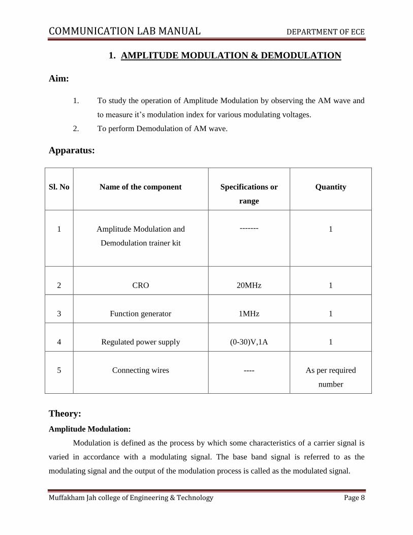
Muffakham Jah college of Engineering & Technology Page 11
for General AM signal and Single–tone AM signal are shown in the following figures. It can be
seen in both cases BW of AM signal is twice the BW of message signal.
COMMUNICATION LAB MANUAL DEPARTMENT OF ECE
Muffakham Jah college of Engineering & Technology Page 12
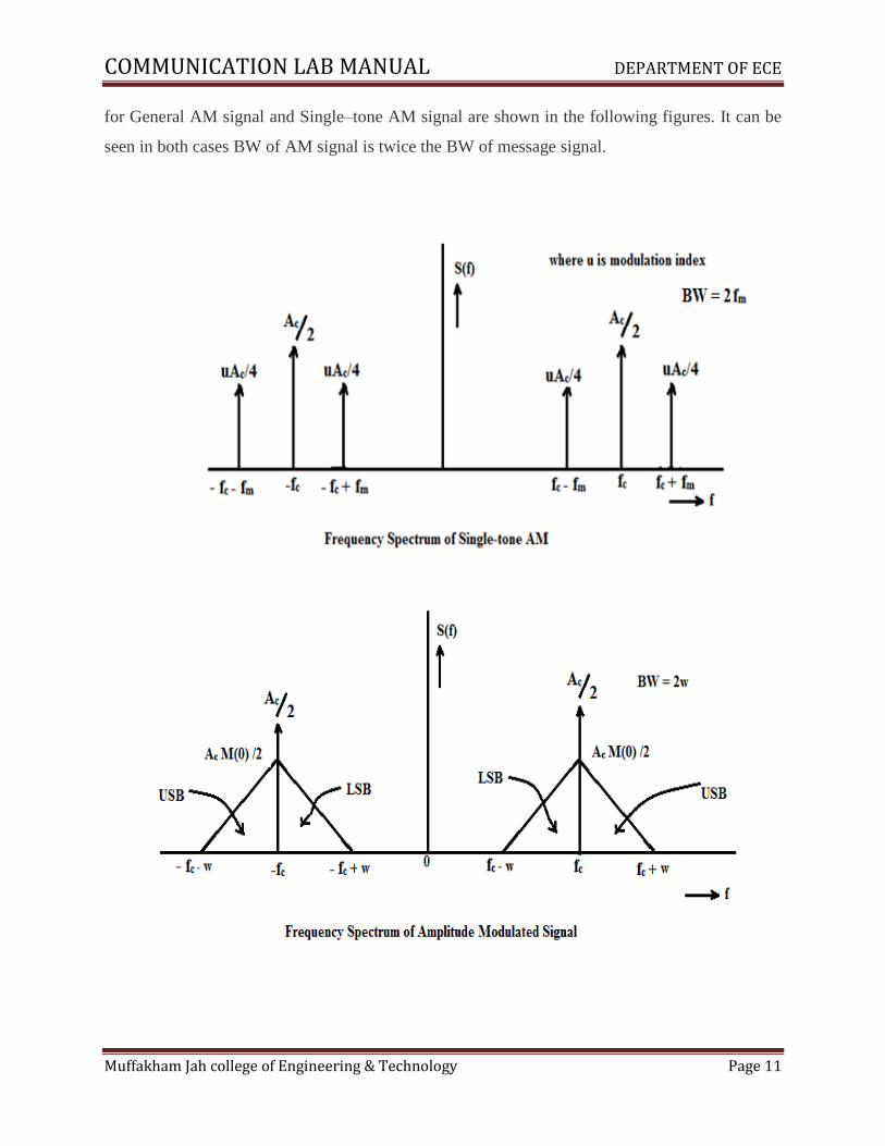
Advantages Disadvantages
It is simple to implement
An amplitude modulation signal is not
efficient in terms of its power usage
It can be demodulated using a circuit
consisting of very few components
It is not efficient in terms of its use of
bandwidth, requiring a bandwidth
equal to twice that of the highest audio
frequency
AM receivers are very cheap as no
specialized components are needed.
An amplitude modulation signal is
prone to high levels of noise because
most noise is amplitude based and
obviously AM detectors are sensitive
to it.
Coverage area of AM receiver is wider
than FM. AM is a long distance
Communication.
AM receivers are less immune to
Noise.
COMMUNICATION LAB MANUAL DEPARTMENT OF ECE
Muffakham Jah college of Engineering & Technology Page 13
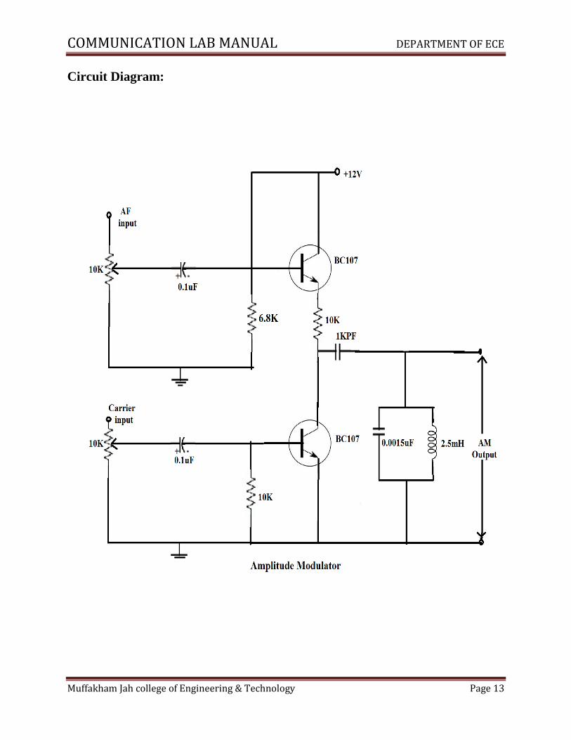
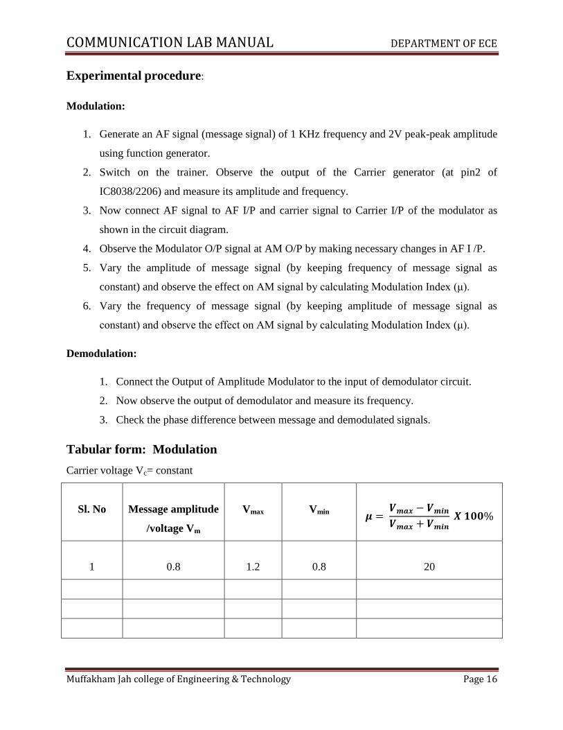
Circuit Diagram:
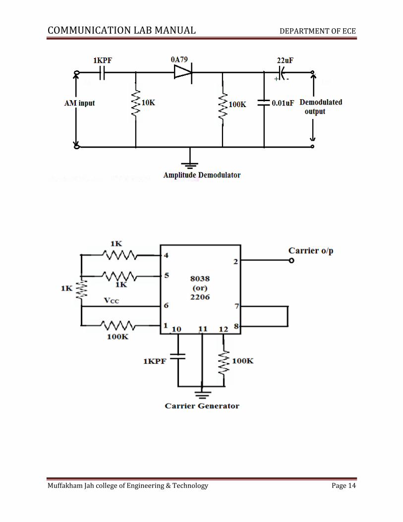
COMMUNICATION LAB MANUAL DEPARTMENT OF ECE
Muffakham Jah college of Engineering & Technology Page 14

COMMUNICATION LAB MANUAL DEPARTMENT OF ECE
Muffakham Jah college of Engineering & Technology Page 15
Model graphs:
COMMUNICATION LAB MANUAL DEPARTMENT OF ECE
Muffakham Jah college of Engineering & Technology Page 16
Experimental procedure:
Modulation:
1. Generate an AF signal (message signal) of 1 KHz frequency and 2V peak-peak amplitude
using function generator.
2. Switch on the trainer. Observe the output of the Carrier generator (at pin2 of
IC8038/2206) and measure its amplitude and frequency.
3. Now connect AF signal to AF I/P and carrier signal to Carrier I/P of the modulator as
shown in the circuit diagram.
4. Observe the Modulator O/P signal at AM O/P by making necessary changes in AF I /P.
5. Vary the amplitude of message signal (by keeping frequency of message signal as
constant) and observe the effect on AM signal by calculating Modulation Index (μ).
6. Vary the frequency of message signal (by keeping amplitude of message signal as
constant) and observe the effect on AM signal by calculating Modulation Index (μ).
Demodulation:
1. Connect the Output of Amplitude Modulator to the input of demodulator circuit.
2. Now observe the output of demodulator and measure its frequency.
3. Check the phase difference between message and demodulated signals.
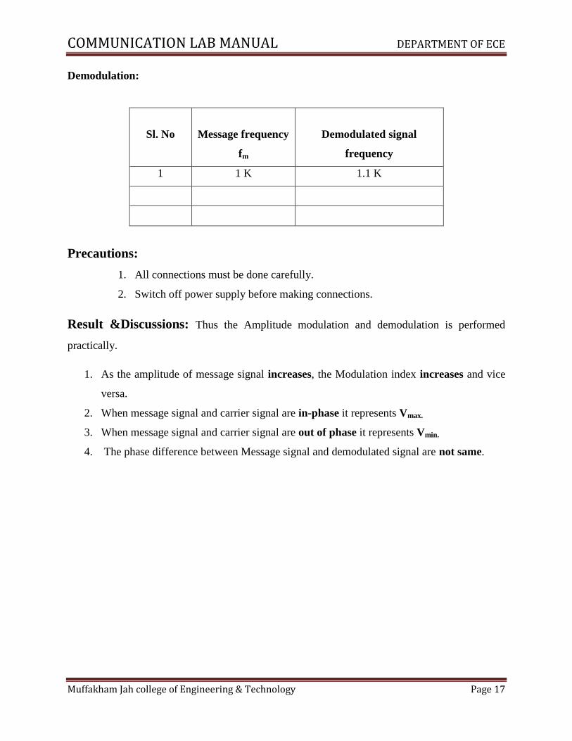
Tabular form: Modulation
Carrier voltage Vc= constant
Sl. No
Message amplitude
/voltage Vm
Vmax
Vmin
𝝁 = 𝑽𝒎𝒂𝒙 − 𝑽𝒎𝒊𝒏
𝑽𝒎𝒂𝒙 + 𝑽𝒎𝒊𝒏 𝑿 𝟏𝟎𝟎%
1
0.8
1.2
0.8
20
COMMUNICATION LAB MANUAL DEPARTMENT OF ECE
Muffakham Jah college of Engineering & Technology Page 17
Demodulation:
Sl. No
Message frequency
fm
Demodulated signal
frequency
1 1 K 1.1 K
Precautions:
1. All connections must be done carefully.
2. Switch off power supply before making connections.
Result &Discussions: Thus the Amplitude modulation and demodulation is performed
practically.
1. As the amplitude of message signal increases, the Modulation index increases and vice
versa.
2. When message signal and carrier signal are in-phase it represents Vmax.
3. When message signal and carrier signal are out of phase it represents Vmin.
4. The phase difference between Message signal and demodulated signal are not same.
COMMUNICATION LAB MANUAL DEPARTMENT OF ECE
Muffakham Jah college of Engineering & Technology Page 18
2. FM MODULATION & DEMODULATION
Aim:
1. To study the operation of Frequency Modulation by observing the FM wave.
2. To measure it‟s modulation index for various modulating voltages and
frequencies.
Apparatus:
Sl. No
Name of the component
Specifications or
range
Quantity
1
frequency Modulation and
Demodulation trainer kit
-------
1
2
CRO
20MHz
1
3
Function generator
1MHz
1
4
Regulated power supply
(0-30)V,1A
1
5
Connecting wires and Probes
----
As per required
number
COMMUNICATION LAB MANUAL DEPARTMENT OF ECE
Muffakham Jah college of Engineering & Technology Page 19
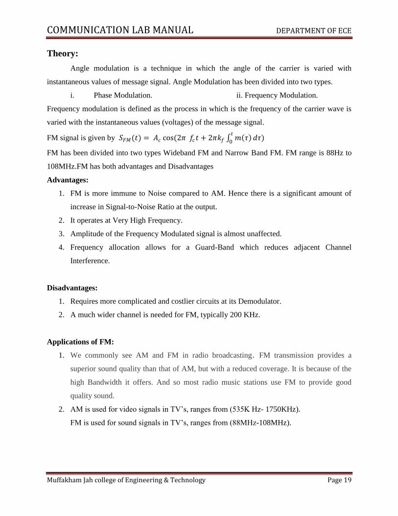
Theory:
Angle modulation is a technique in which the angle of the carrier is varied with
instantaneous values of message signal. Angle Modulation has been divided into two types.
i. Phase Modulation. ii. Frequency Modulation.
Frequency modulation is defined as the process in which is the frequency of the carrier wave is
varied with the instantaneous values (voltages) of the message signal.
FM signal is given by 𝑆𝐹𝑀(𝑡) = 𝐴𝑐 cos(2𝜋 𝑓𝑐𝑡 + 2𝜋𝑘𝑓 𝑚 𝜏 𝑡
0𝑑𝜏)
FM has been divided into two types Wideband FM and Narrow Band FM. FM range is 88Hz to
108MHz.FM has both advantages and Disadvantages
Advantages:
1. FM is more immune to Noise compared to AM. Hence there is a significant amount of
increase in Signal-to-Noise Ratio at the output.
2. It operates at Very High Frequency.
3. Amplitude of the Frequency Modulated signal is almost unaffected.
4. Frequency allocation allows for a Guard-Band which reduces adjacent Channel
Interference.
Disadvantages:
1. Requires more complicated and costlier circuits at its Demodulator.
2. A much wider channel is needed for FM, typically 200 KHz.
Applications of FM:
1. We commonly see AM and FM in radio broadcasting. FM transmission provides a
superior sound quality than that of AM, but with a reduced coverage. It is because of the
high Bandwidth it offers. And so most radio music stations use FM to provide good
quality sound.
2. AM is used for video signals in TV‟s, ranges from (535K Hz- 1750KHz).
FM is used for sound signals in TV‟s, ranges from (88MHz-108MHz).
COMMUNICATION LAB MANUAL DEPARTMENT OF ECE
Muffakham Jah college of Engineering & Technology Page 20
Frequency Modulation Amplitude Modulation
FM receivers are more immune to Noise. AM receivers are not immune to Noise.
All Transmitted power is useful, no power is wasted Carrier and Side Band power is wasted.
Transmitter and Receiver circuits are complex. Uses simple Transmitter and Receiver
Circuits.
BW is higher and depends on modulation index BW is low and is independent of Modulation
index
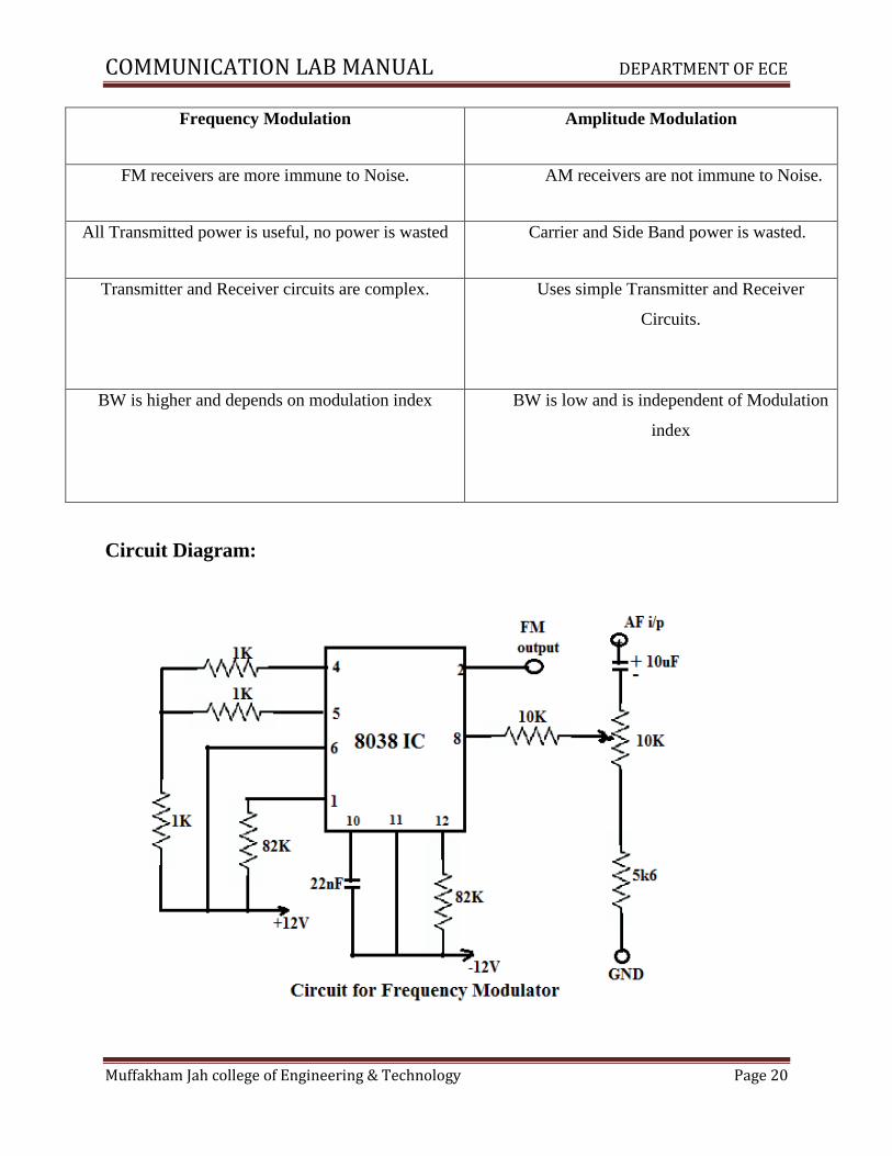
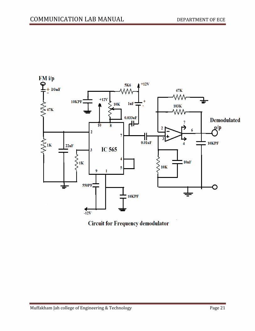
Circuit Diagram:
COMMUNICATION LAB MANUAL DEPARTMENT OF ECE
Muffakham Jah college of Engineering & Technology Page 21
COMMUNICATION LAB MANUAL DEPARTMENT OF ECE
Muffakham Jah college of Engineering & Technology Page 22
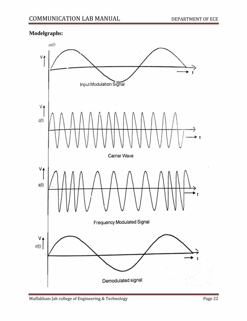
Modelgraphs:

COMMUNICATION LAB MANUAL DEPARTMENT OF ECE
Muffakham Jah college of Engineering & Technology Page 23
Experimental procedure:
Modulation:
1. Switch on the trainer kit.
2. Connect CRO to the FM output and observe carrier frequency (and amplitude) of the
wave at that point without any AF input.
3. Connect around (3 kHz to 10 kHz) with 2.4 volts sine wave (AF signal) to the AF input
of the frequency Modulator.
4. Now observe the FM output on the first channel of CRO and adjust the amplitude of AF
signal to get clear FM wave form.
5. Vary the modulating amplitude and frequency of the message signal and observe the
effect on FM output.
6. Calculate modulation index in the first case by changing frequency of message signal (by
keeping amplitude as constant).
7. Calculate modulation index in the second case by changing amplitude of message
signal(by keeping frequency as constant)
Demodulation:
1. Connect the FM output to the FM input of Demodulator circuit .Observe the
demodulated wave (second channel of CRO).
2. By vary the potentiometer provided in the demodulator section and see the output.
Tabular form: Modulation
Message frequency fm= constant
Sl. No
Message
amplitude
/voltage Vm
Fmax
Fmin
∆𝒇 =𝑭𝒎𝒂𝒙 − 𝑭𝒎𝒊𝒏
𝟐
𝜷 = ∆𝒇
𝒇𝒎

COMMUNICATION LAB MANUAL DEPARTMENT OF ECE
Muffakham Jah college of Engineering & Technology Page 24
Message amplitude Vm= constant
Sl. No
Message
frequency fm
Fmax
Fmin
∆𝒇 =𝑭𝒎𝒂𝒙 − 𝑭𝒎𝒊𝒏
𝟐
𝜷 = ∆𝒇
𝒇𝒎
Demoulation:
Sl.No Message frequency Demodulated frequency
Precautions:
1. All connections must be done carefully.
2. Switch off power supply before making connections.
Result & Discussions:
Thus the Frequency modulation and demodulation are performed practically.
1. Modulation index β decreases with respect to frequency of message signal when the
amplitude of message signal is kept constant.
2. Modulation index β increases with respect to amplitude of message signal when the
frequency of message signal is kept constant.
COMMUNICATION LAB MANUAL DEPARTMENT OF ECE
Muffakham Jah college of Engineering & Technology Page 25
3. PRE-EMPHASIS & DE-EMPHASIS
Aim:
To observe the effect of Pre-emphasis and De-emphasis on a given signal.
Apparatus:
Sl. No
Name of the component
Specifications or range
Quantity
1
Resistors
7.5KΩ,6.8KΩ
1 each
2
Capacitors
10nF,0.1µF
1each
3
Function generator
1MHz
1
4
CRO
20MHz
1
5
Connecting wires
----
As per required
number
Theory:
The noise has greater effect on high frequencies than on the lower ones. Thus, if the higher frequencies
were artificially boosted at the transmitter and correspondingly cut at the receiver, an improvement in
noise immunity could be expected, thereby increasing the SNR ratio. This boosting of the higher
modulating frequencies at the transmitter is known as pre-emphasis and the compensation at the receiver
is called as de-emphasis.
COMMUNICATION LAB MANUAL DEPARTMENT OF ECE
Muffakham Jah college of Engineering & Technology Page 26
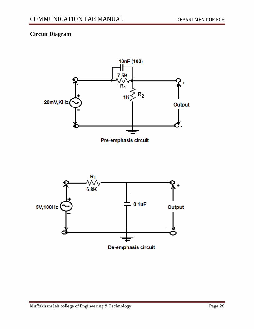
Circuit Diagram:
COMMUNICATION LAB MANUAL DEPARTMENT OF ECE
Muffakham Jah college of Engineering & Technology Page 27
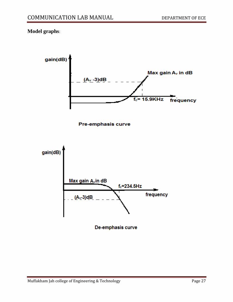
Model graphs:
COMMUNICATION LAB MANUAL DEPARTMENT OF ECE
Muffakham Jah college of Engineering & Technology Page 28
Experimental procedure:
1. Connect the circuit diagram as per pre-emphasis circuit shown in figure.
2. Apply a sinusoidal signal of 20mV as input signal to pre-emphasis circuit.
3. Then by increasing the input signal frequency from 500Hz to 20 kHz. Observe the
output voltage Vo and calculate gain in dB as 20 log𝑉𝑜
𝑉𝑖 .
4. Similarly apply a sinusoidal signal of 5V, 100Hz to de-emphasis circuit .vary the
input signal frequency from 100Hz to 20 KHz and calculate gain in dB as 20 log𝑉𝑜
𝑉𝑖
by observing output voltage Vo.
5. Plot pre-emphasis and de-emphasis curves.
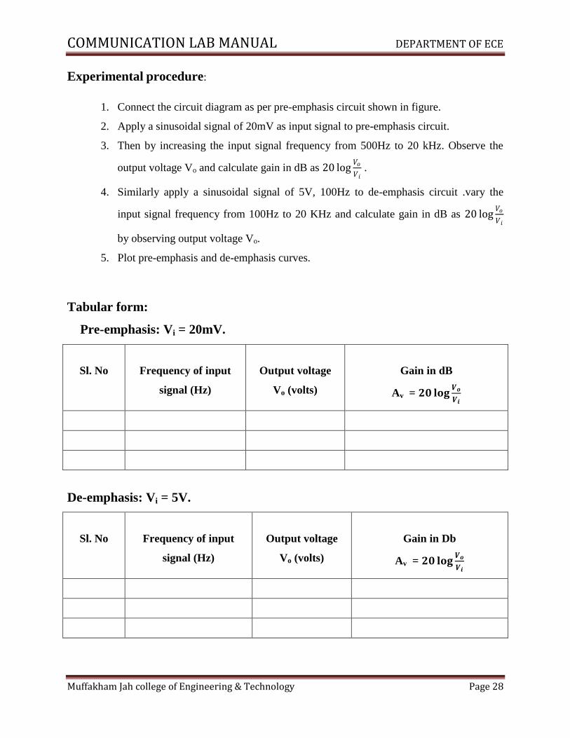
Tabular form:
Pre-emphasis: Vi = 20mV.
Sl. No
Frequency of input
signal (Hz)
Output voltage
Vo (volts)
Gain in dB
Av = 𝟐𝟎 𝐥𝐨𝐠𝑽𝒐
𝑽𝒊
De-emphasis: Vi = 5V.
Sl. No
Frequency of input
signal (Hz)
Output voltage
Vo (volts)
Gain in Db
Av = 𝟐𝟎 𝐥𝐨𝐠𝑽𝒐
𝑽𝒊
COMMUNICATION LAB MANUAL DEPARTMENT OF ECE
Muffakham Jah college of Engineering & Technology Page 29
Precautions:
1. All connections must be done carefully.
2. Switch off power supply before making connections.
Result & Discussions:
The effect of Pre-emphasis and De-emphasis on a given input signal is observed.
COMMUNICATION LAB MANUAL DEPARTMENT OF ECE
Muffakham Jah college of Engineering & Technology Page 30
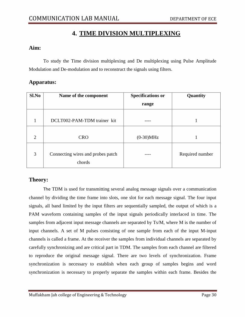
4. TIME DIVISION MULTIPLEXING
Aim:
To study the Time division multiplexing and De multiplexing using Pulse Amplitude
Modulation and De-modulation and to reconstruct the signals using filters.
Apparatus:
Sl.No Name of the component Specifications or
range
Quantity
1
DCLT002-PAM-TDM trainer kit
----
1
2
CRO
(0-30)MHz
1
3
Connecting wires and probes patch
chords
----
Required number
Theory:
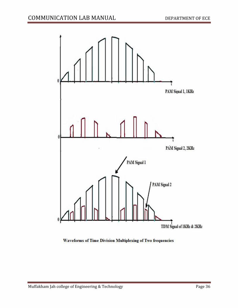
The TDM is used for transmitting several analog message signals over a communication
channel by dividing the time frame into slots, one slot for each message signal. The four input
signals, all band limited by the input filters are sequentially sampled, the output of which is a
PAM waveform containing samples of the input signals periodically interlaced in time. The
samples from adjacent input message channels are separated by Ts/M, where M is the number of
input channels. A set of M pulses consisting of one sample from each of the input M-input
channels is called a frame. At the receiver the samples from individual channels are separated by
carefully synchronizing and are critical part in TDM. The samples from each channel are filtered
to reproduce the original message signal. There are two levels of synchronization. Frame
synchronization is necessary to establish when each group of samples begins and word
synchronization is necessary to properly separate the samples within each frame. Besides the
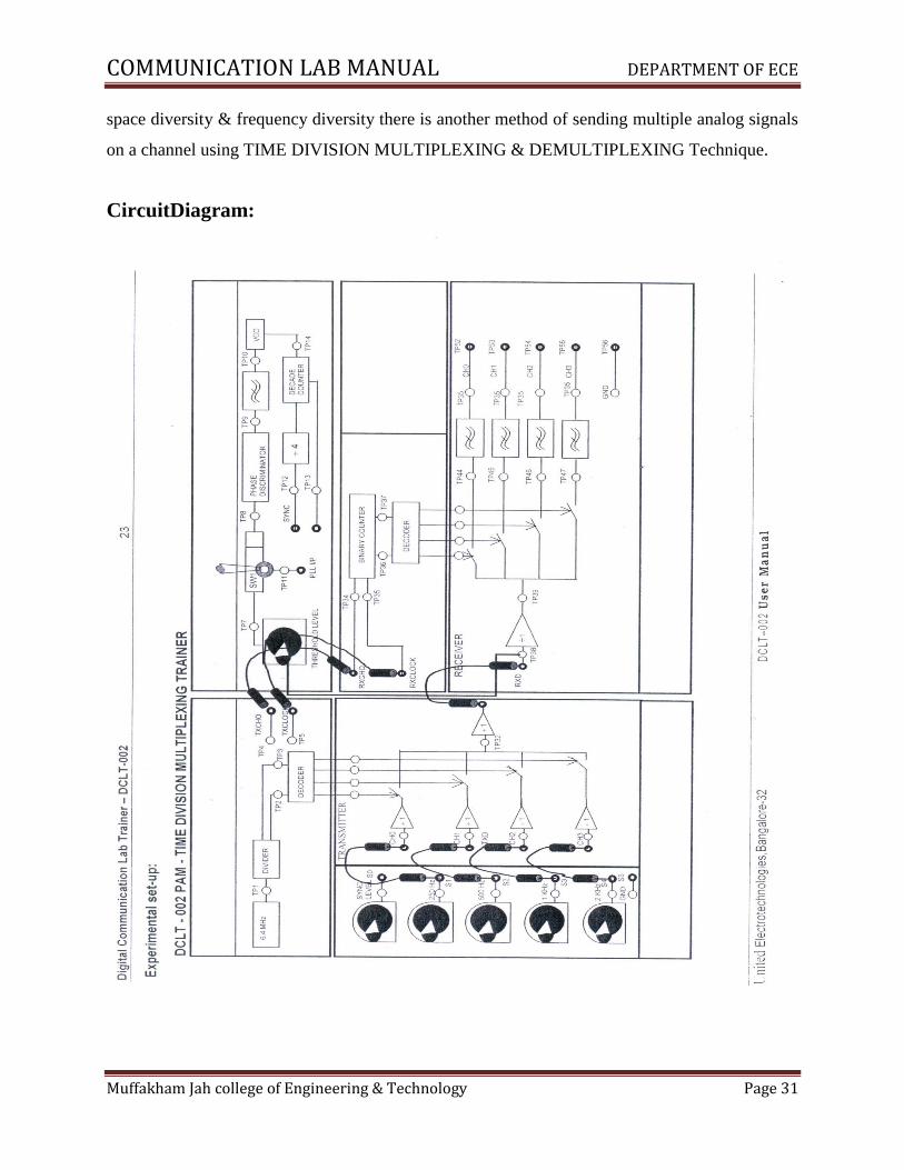
COMMUNICATION LAB MANUAL DEPARTMENT OF ECE
Muffakham Jah college of Engineering & Technology Page 31
space diversity & frequency diversity there is another method of sending multiple analog signals
on a channel using TIME DIVISION MULTIPLEXING & DEMULTIPLEXING Technique.
CircuitDiagram:
COMMUNICATION LAB MANUAL DEPARTMENT OF ECE
Muffakham Jah college of Engineering & Technology Page 32
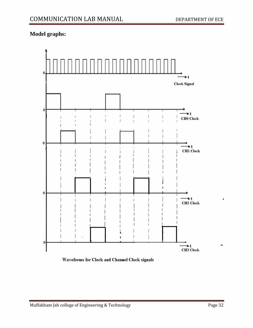
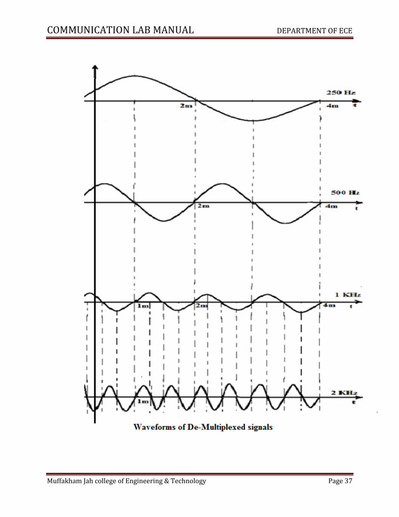
Model graphs:
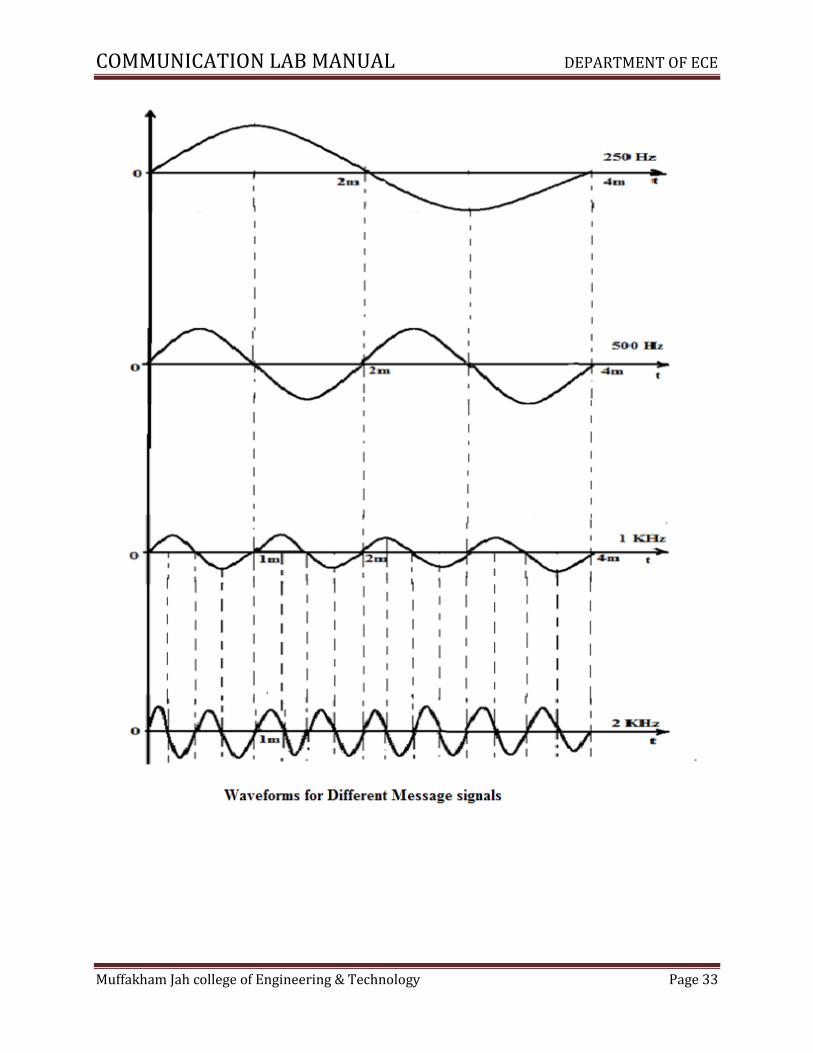
COMMUNICATION LAB MANUAL DEPARTMENT OF ECE
Muffakham Jah college of Engineering & Technology Page 33

COMMUNICATION LAB MANUAL DEPARTMENT OF ECE
Muffakham Jah college of Engineering & Technology Page 34
COMMUNICATION LAB MANUAL DEPARTMENT OF ECE
Muffakham Jah college of Engineering & Technology Page 35
COMMUNICATION LAB MANUAL DEPARTMENT OF ECE
Muffakham Jah college of Engineering & Technology Page 36
COMMUNICATION LAB MANUAL DEPARTMENT OF ECE
Muffakham Jah college of Engineering & Technology Page 37

COMMUNICATION LAB MANUAL DEPARTMENT OF ECE
Muffakham Jah college of Engineering & Technology Page 38
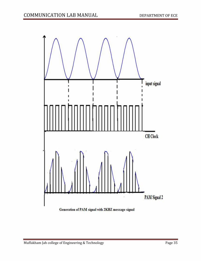
Experimental procedure:
Multiplexing:
1. Observe four input signals at pins S1, S2, S3 and S4 and the Sync level S0 and clock
signals for CH0, CH1, CH2 and CH3 on the trainer kit.
2. Connect either any two channel inputs of 250 Hz, 500 Hz, 1 KHz, 2 KHz or all inputs to
the input of transmitter at CH0, CH1, CH2 and CH3 respectively.
3. Observe multiplexed data at TDX (Transmitter Data) of PAM-TDM transmitter. Thus
the signal is a multiplexed version of two signals or four signals.
De-Multiplexing:
1. Connect TXCLOCK (Transmitter clock) to RXCLOCK (Receiver clock).
2. Connect TXCH0 (Transmitter sync) to RXCH0 (Receiver sync).
3. Connect the TXD (Transmitter data) to RXD (Receiver data).
4. Observe multiplexed data at TDX for four input signals, Transmitter clock at TXCLOCK
and transmitter sync at TXSYNC.
5. Observe the de multiplexed signals at the receiver across the output of fourth order low
pass filter at CH0, CH1, CH2 and CH3.
Precautions:
1. All connections must be done carefully.
2. Switch off power supply before making connections.
Results & Discussions: Thus the Time Division Multiplexing and de multiplexing of analog
signals using PAM-TDM trainer kit is performed and the waveforms are observed.
COMMUNICATION LAB MANUAL DEPARTMENT OF ECE
Muffakham Jah college of Engineering & Technology Page 39
5. A. SAMPLING AND RECONSTRUCTION
Aim:
To study the signal sampling and its reconstruction.
Apparatus:
Sl.No
Name of the component
Specifications or
range
Quantity
1
Sampling theorem verification trainer
kit-DCLT001
-
1
2
CRO
20MHz
1
3
Connecting wires and patch chords
--
Based on requirement
Theory:
An analog Source of information produces an output that can have any one of a
continuum of possible value at any time. The sound pressure from an Orchestra playing music is
an example for analog source. There no of analog sources a signal generator is another analog
source. An analog signal is an electrical waveform that can have any one of continuous
amplitudes at any time. Voltage and current are examples of CT signals.
A digital source can be defined as the one which generates digital signals most sources
are analog in nature and by using some mechanism an analog source can be converted into a

COMMUNICATION LAB MANUAL DEPARTMENT OF ECE
Muffakham Jah college of Engineering & Technology Page 40
digital source. For example, temperature is an analog quantity, but when combined with a
thermostat with output values of on or off, the combination may be considered as a digital
source.
A digital signal may be defined as an electrical waveform having one of a finite set of
possible amplitudes at any time. i.e, a binary signal is a digital signal. A communication system
is required to transport an information bearing signal from a source to destination through a
communication channel. Basically, a communication system may be analog or digital type. In an
analog communication system, the information-bearing signal is continuously varying in both
amplitude and time, and it is used directly to modify some characteristic of a sinusoidal carrier
wave, such as amplitude, phase or frequency. In Digital Communication system, on the other
hand the m(t) is processed so that it can be represented by a sequence of discrete messages.
Need for Digital Communications: The growth of Digital Communications is largely due to the
following reasons:
1. Digital communications provide improved reliability.
2. The availability of wide band channels provided by geo-stationary satellites, Optical fibers and
Co-axial cables.
3. The ever increasing availability of integrated Solid-state technology, which has made it
possible to increase system complexity by orders of magnitude in a cost effective manner.
As we observed the advantages of digital communications, there is every possible need for
converting the analog signal to digital form for compatibility. Three basic operations are
combined to convert an analog signal to a digital signal by
Sampling: In the sampling process only sample value of the analog signal at uniformly spaced
discrete instant of time are extracted and retained. i.e a continuous time signal is converted into a
discrete signal.
Quantizing: In this the nearest level in a finite set of discrete levels approximates each sample
value.
Encoding: In encoding, the selected level is represented by a code word that consists of a
prescribed number of code elements.
Sampling theorem: The analog signal can be converted to a discrete time signal by a process
called sampling. The Sampling theorem for a band limited (W Hz) signal of finite energy can be
stated as follows that

COMMUNICATION LAB MANUAL DEPARTMENT OF ECE
Muffakham Jah college of Engineering & Technology Page 41
„‟A band limited signal of finite energy, which has no frequency component higher than
W Hz is Completely described by specifying the values of the signal at instants of time separated
by 1/2W Seconds.‟‟ It can be recovered from knowledge of samples taken at the rate of 2W
samples per second.
Circuit Diagram:
COMMUNICATION LAB MANUAL DEPARTMENT OF ECE
Muffakham Jah college of Engineering & Technology Page 42
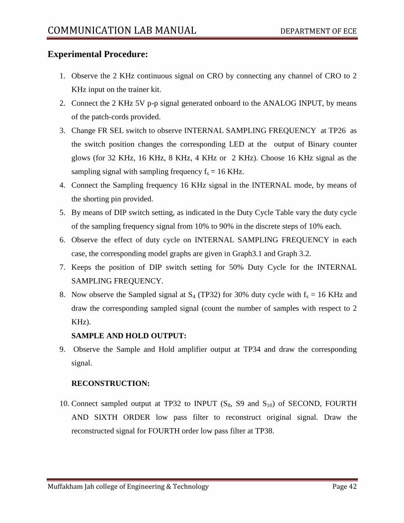
Experimental Procedure:
1. Observe the 2 KHz continuous signal on CRO by connecting any channel of CRO to 2
KHz input on the trainer kit.
2. Connect the 2 KHz 5V p-p signal generated onboard to the ANALOG INPUT, by means
of the patch-cords provided.
3. Change FR SEL switch to observe INTERNAL SAMPLING FREQUENCY at TP26 as
the switch position changes the corresponding LED at the output of Binary counter
glows (for 32 KHz, 16 KHz, 8 KHz, 4 KHz or 2 KHz). Choose 16 KHz signal as the
sampling signal with sampling frequency fs = 16 KHz.
4. Connect the Sampling frequency 16 KHz signal in the INTERNAL mode, by means of
the shorting pin provided.
5. By means of DIP switch setting, as indicated in the Duty Cycle Table vary the duty cycle
of the sampling frequency signal from 10% to 90% in the discrete steps of 10% each.
6. Observe the effect of duty cycle on INTERNAL SAMPLING FREQUENCY in each
case, the corresponding model graphs are given in Graph3.1 and Graph 3.2.
7. Keeps the position of DIP switch setting for 50% Duty Cycle for the INTERNAL
SAMPLING FREQUENCY.
8. Now observe the Sampled signal at S4 (TP32) for 30% duty cycle with fs = 16 KHz and
draw the corresponding sampled signal (count the number of samples with respect to 2
KHz).
SAMPLE AND HOLD OUTPUT:
9. Observe the Sample and Hold amplifier output at TP34 and draw the corresponding
signal.
RECONSTRUCTION:
10. Connect sampled output at TP32 to INPUT (S8, S9 and S10) of SECOND, FOURTH
AND SIXTH ORDER low pass filter to reconstruct original signal. Draw the
reconstructed signal for FOURTH order low pass filter at TP38.
COMMUNICATION LAB MANUAL DEPARTMENT OF ECE
Muffakham Jah college of Engineering & Technology Page 43
11. Connect sample and hold output at TP34 to INPUT (S8, S9 and S10) of SECOND,
FOURTH AND SIXTH ORDER low pass filter to reconstruct original signal. Draw the
reconstructed signal for FOURTH order low pass filter at TP38.
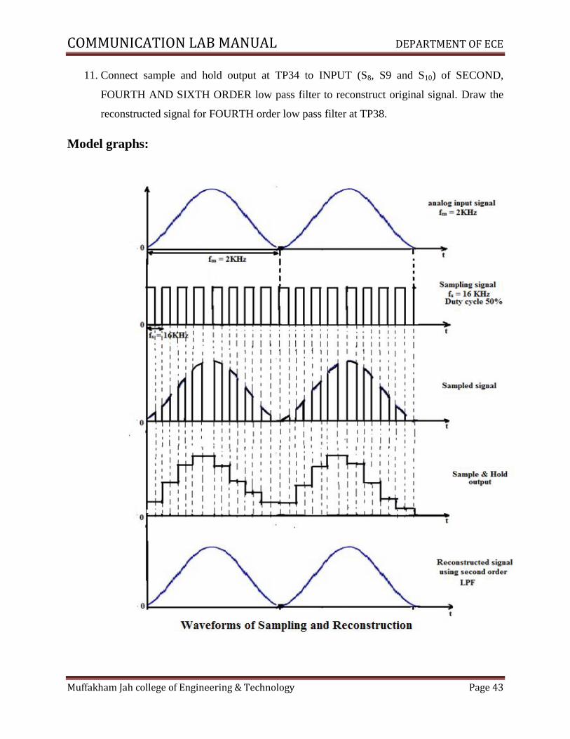
Model graphs:

COMMUNICATION LAB MANUAL DEPARTMENT OF ECE
Muffakham Jah college of Engineering & Technology Page 44
Precautions:
1. Connections must be done carefully.
2. Switch of the power supply before making connections.
Result & discussions:
1. Sampling of a signal and its reconstruction is performed practically.
2. The effect of duty cycle of the sampling frequency on the sampled signal is observed.
3. The effect of duty cycle on Sample and hold output signal is observed.
COMMUNICATION LAB MANUAL DEPARTMENT OF ECE
Muffakham Jah college of Engineering & Technology Page 45
5. B. PULSE AMPLITUDE MODULATION
Aim:
To study the Pulse Amplitude Modulation and Demodulation using FT1503 Trainer.
Apparatus:
Sl.No
Name of the component
Specifications or
range
Quantity
1
PAM Modulation and Demodulation
experimental kit.( Built in DC Power
supply +/- 5V /350 mA, ICs provided
on the board TL084.LM565, 74LS163
each 1no, Provided with 2mm
Sockets.)
-
1
2
CRO
20MHz
1
3
Connecting wires, Probes and patch
chords
--
Based on requirement
Theory:
Pulse Modulation may be used to transmit analog information, such as continuous speech
or data. It is a system in which continuous waveforms are sampled at regular
intervals.Information regarding the signal is transmitted only at the sampling times, together with

COMMUNICATION LAB MANUAL DEPARTMENT OF ECE
Muffakham Jah college of Engineering & Technology Page 46
any synchronizing pulse that may be required. At the receiving end, the original waveforms may
be reconstructed from the information regarding the samples, if these are taken frequently
enough. Despite the fact that information about the signal is not supplied continuously, As in
Amplitude and Frequency modulation , the resulting receiver output can have regenerate the
analog information signal.
Pulse Modulation may be subdivided broadly into two categories, Analog and Digital. In
the former, the indication of sample Amplitude may be continuously variable, while in the later a
code which indicates the sample amplitude to the nearest predetermined level is sent. Pulse
Amplitude modulation is a form of analog communication which is discussed in the following
section.
Pulse Amplitude Modulation
In this we have a train of fixed width of pulses. The amplitude of each pulse is made
proportional to the amplitude of the modulating signal at that instant. In the PAM generation
circuit, Synchronous clock is applied to the base of the transistor. Modulating signal is applied to
the (unipolar positive) is given to the collector of the transistor. The output of the transistor
(Collector current) varies in accordance with the amplitude of the modulating signal voltage
resulting in modulated output.
Pulse Amplitude Demodulation
The Demodulation of Pulse Amplitude Modulation is quite a simple process. PAM signal
is fed to a Low Pass Filter, from which the Demodulating signal emerges, whose amplitude at
any time is proportional to the PAM at that time. This signal is given to an inverting amplifier to
amplify its level. The demodulated output is almost equal amplitude with the modulating signal
but is in phase shifted due to the modulation, demodulation process.
1 KHz Signal source (AF)
The circuit shown in the following figure uses two op-amps, one acting as non-inverting
integrator and the other one as inverting integrator. The two op-amps are connected in cascade to
form a feedback loop .the circuit oscillates with sinusoidal output. The sinusoidal oscillation
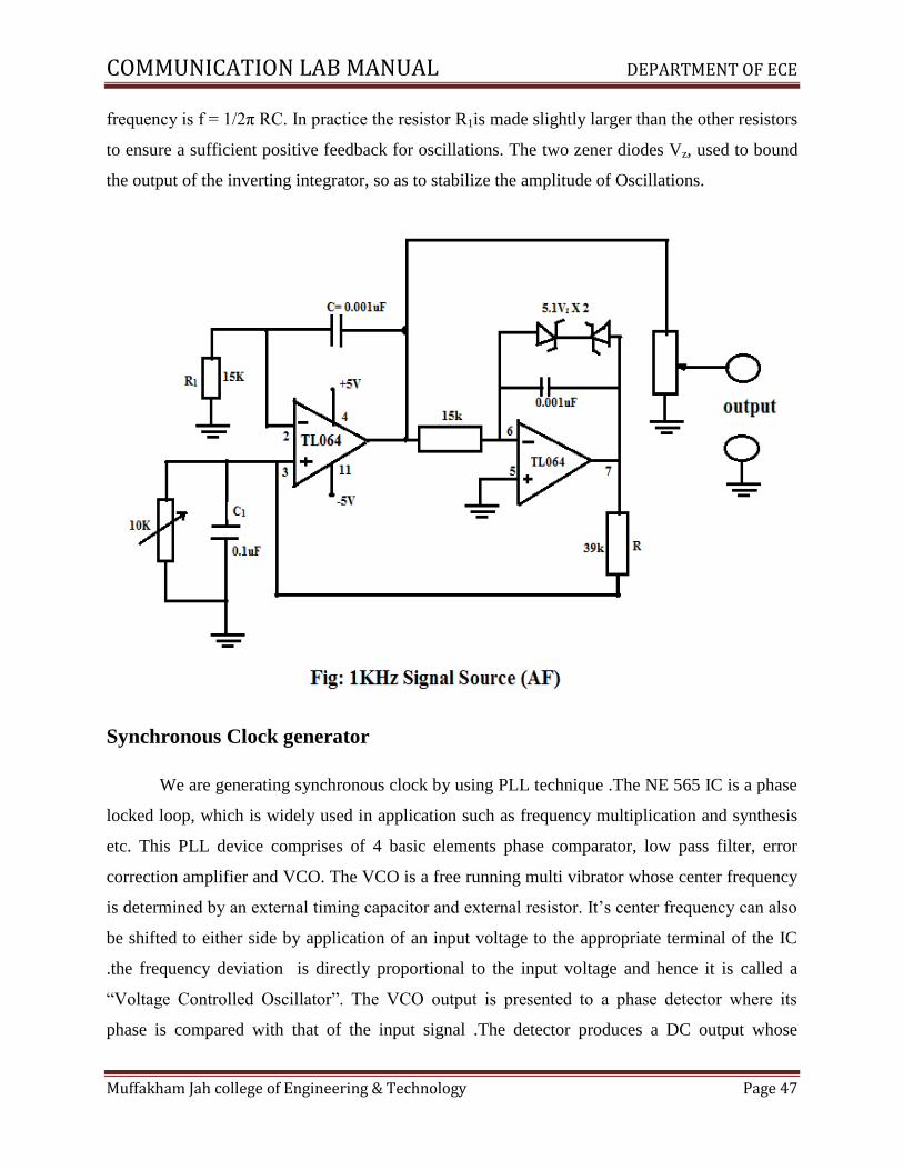
COMMUNICATION LAB MANUAL DEPARTMENT OF ECE
Muffakham Jah college of Engineering & Technology Page 47
frequency is f = 1/2π RC. In practice the resistor R1is made slightly larger than the other resistors
to ensure a sufficient positive feedback for oscillations. The two zener diodes Vz, used to bound
the output of the inverting integrator, so as to stabilize the amplitude of Oscillations.
Synchronous Clock generator
We are generating synchronous clock by using PLL technique .The NE 565 IC is a phase
locked loop, which is widely used in application such as frequency multiplication and synthesis
etc. This PLL device comprises of 4 basic elements phase comparator, low pass filter, error
correction amplifier and VCO. The VCO is a free running multi vibrator whose center frequency
is determined by an external timing capacitor and external resistor. It‟s center frequency can also
be shifted to either side by application of an input voltage to the appropriate terminal of the IC
.the frequency deviation is directly proportional to the input voltage and hence it is called a
“Voltage Controlled Oscillator”. The VCO output is presented to a phase detector where its
phase is compared with that of the input signal .The detector produces a DC output whose
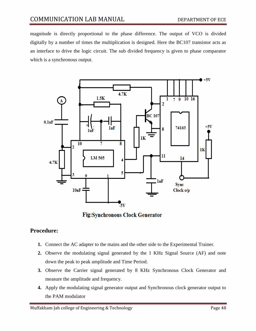
COMMUNICATION LAB MANUAL DEPARTMENT OF ECE
Muffakham Jah college of Engineering & Technology Page 48
magnitude is directly proportional to the phase difference. The output of VCO is divided
digitally by a number of times the multiplication is designed. Here the BC107 transistor acts as
an interface to drive the logic circuit. The sub divided frequency is given to phase comparator
which is a synchronous output.
Procedure:
1. Connect the AC adapter to the mains and the other side to the Experimental Trainer.
2. Observe the modulating signal generated by the 1 KHz Signal Source (AF) and note
down the peak to peak amplitude and Time Period.
3. Observe the Carrier signal generated by 8 KHz Synchronous Clock Generator and
measure the amplitude and frequency.
4. Apply the modulating signal generator output and Synchronous clock generator output to
the PAM modulator
COMMUNICATION LAB MANUAL DEPARTMENT OF ECE
Muffakham Jah college of Engineering & Technology Page 49
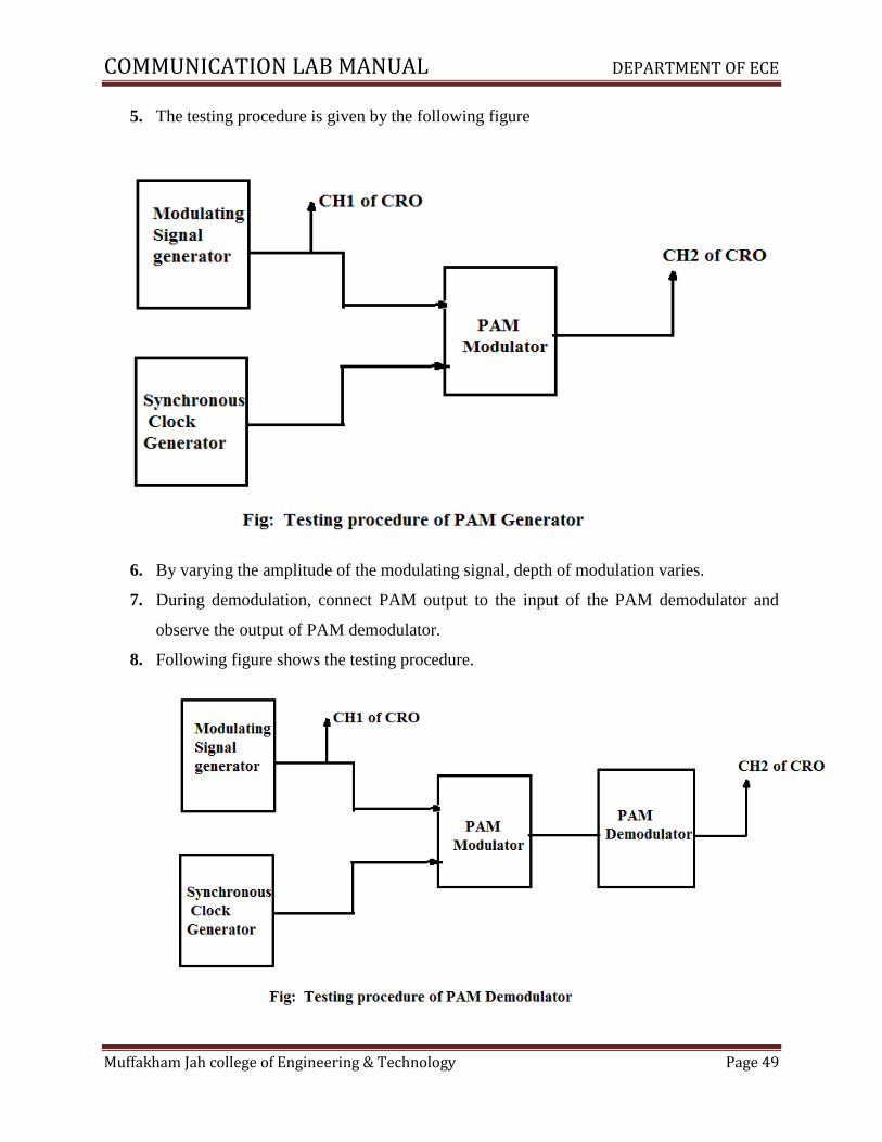
5. The testing procedure is given by the following figure
6. By varying the amplitude of the modulating signal, depth of modulation varies.
7. During demodulation, connect PAM output to the input of the PAM demodulator and
observe the output of PAM demodulator.
8. Following figure shows the testing procedure.

COMMUNICATION LAB MANUAL DEPARTMENT OF ECE
Muffakham Jah college of Engineering & Technology Page 50
Circuit Diagram:

COMMUNICATION LAB MANUAL DEPARTMENT OF ECE
Muffakham Jah college of Engineering & Technology Page 51
Model graphs:
COMMUNICATION LAB MANUAL DEPARTMENT OF ECE
Muffakham Jah college of Engineering & Technology Page 52
Precautions:
1. All Connections must be done carefully.
2. Switch off the power supply while making Connections.
Result & Discussions:
Pulse Amplitude Modulation and Demodulation is performed using FT1503 trainer. And the
modulated and demodulated waveforms were observed.
COMMUNICATION LAB MANUAL DEPARTMENT OF ECE
Muffakham Jah college of Engineering & Technology Page 53
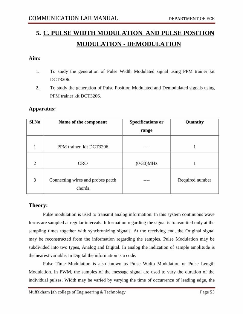
5. C. PULSE WIDTH MODULATION AND PULSE POSITION
MODULATION - DEMODULATION
Aim:
1. To study the generation of Pulse Width Modulated signal using PPM trainer kit
DCT3206.
2. To study the generation of Pulse Position Modulated and Demodulated signals using
PPM trainer kit DCT3206.
Apparatus:
Sl.No Name of the component Specifications or
range
Quantity
1
PPM trainer kit DCT3206
----
1
2
CRO
(0-30)MHz
1
3
Connecting wires and probes patch
chords
----
Required number
Theory:
Pulse modulation is used to transmit analog information. In this system continuous wave
forms are sampled at regular intervals. Information regarding the signal is transmitted only at the
sampling times together with synchronizing signals. At the receiving end, the Original signal
may be reconstructed from the information regarding the samples. Pulse Modulation may be
subdivided into two types, Analog and Digital. In analog the indication of sample amplitude is
the nearest variable. In Digital the information is a code.
Pulse Time Modulation is also known as Pulse Width Modulation or Pulse Length
Modulation. In PWM, the samples of the message signal are used to vary the duration of the
individual pulses. Width may be varied by varying the time of occurrence of leading edge, the
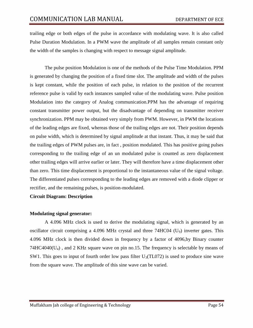
COMMUNICATION LAB MANUAL DEPARTMENT OF ECE
Muffakham Jah college of Engineering & Technology Page 54
trailing edge or both edges of the pulse in accordance with modulating wave. It is also called
Pulse Duration Modulation. In a PWM wave the amplitude of all samples remain constant only
the width of the samples is changing with respect to message signal amplitude.
The pulse position Modulation is one of the methods of the Pulse Time Modulation. PPM
is generated by changing the position of a fixed time slot. The amplitude and width of the pulses
is kept constant, while the position of each pulse, in relation to the position of the recurrent
reference pulse is valid by each instances sampled value of the modulating wave. Pulse position
Modulation into the category of Analog communication.PPM has the advantage of requiring
constant transmitter power output, but the disadvantage of depending on transmitter receiver
synchronization. PPM may be obtained very simply from PWM. However, in PWM the locations
of the leading edges are fixed, whereas those of the trailing edges are not. Their position depends
on pulse width, which is determined by signal amplitude at that instant. Thus, it may be said that
the trailing edges of PWM pulses are, in fact , position modulated. This has positive going pulses
corresponding to the trailing edge of an un modulated pulse is counted as zero displacement
other trailing edges will arrive earlier or later. They will therefore have a time displacement other
than zero. This time displacement is proportional to the instantaneous value of the signal voltage.
The differentiated pulses corresponding to the leading edges are removed with a diode clipper or
rectifier, and the remaining pulses, is position-modulated.
Circuit Diagram: Description
Modulating signal generator:
A 4.096 MHz clock is used to derive the modulating signal, which is generated by an
oscillator circuit comprising a 4.096 MHz crystal and three 74HC04 (U9) inverter gates. This
4.096 MHz clock is then divided down in frequency by a factor of 4096,by Binary counter
74HC4040(U4) , and 2 KHz square wave on pin no.15. The frequency is selectable by means of
SW1. This goes to input of fourth order low pass filter U3(TL072) is used to produce sine wave
from the square wave. The amplitude of this sine wave can be varied.

COMMUNICATION LAB MANUAL DEPARTMENT OF ECE
Muffakham Jah college of Engineering & Technology Page 55
Modulation:
The circuit uses 555IC (U1) a mono stable multi vibrator to perform the PPM. The
message signal is given to pin no.5 & at pin no.2 the pulse carrier is of 32KHz frequency is
connected internally & PWM, Differentiated PWM outputs are available at pins TP4,TP5.This
differentiated output is fed to the 555 IC(U2) in mono stable mode pin no.2. The PPM output is
available at pin no 6.
Model graphs:

COMMUNICATION LAB MANUAL DEPARTMENT OF ECE
Muffakham Jah college of Engineering & Technology Page 56
Circuit Diagram:

COMMUNICATION LAB MANUAL DEPARTMENT OF ECE
Muffakham Jah college of Engineering & Technology Page 57
Experimental procedure:
Procedure for PWM: modulation
1. Observe the signal generated by the Modulating signal generator at pin TP1 by
connecting any channel of the CRO by keeping frequency in 1 KHz position and
amplitude pot in max position.
2. Observe the pulse carrier signal at pin no2 TP3 of the 555 IC (U1) measure its amplitude
and time period.
3. Now interconnect TP1 of modulating signal generator with TP2 of 555IC (U1) using
connecting wire.
4. Switch on the power supply, observe the PWM wave in CH1 of CRO with respect to
modulating signal in CH2 of CRO.
5. Plot the PWM wave carefully by counting the total number of pulses with respect to one
complete cycle of message signal. And measure maximum and minimum durations of
PWM wave at positive and negative peaks of modulating signal.
Procedure for PPM: modulation
1. Observe the signal generated by the Modulating signal generator at pin TP1 by
connecting any channel of the CRO by keeping frequency in 1 KHz position and
amplitude pot in max position.
2. Observe the pulse carrier signal at pin no2 TP3 of the 555 IC (U1) measure its amplitude
and time period.
3. Now interconnect TP1 of modulating signal generator with TP2 of 555IC (U1) using
connecting wire.
4. Switch on the power supply, observe the PPM output at TP6 in CH1 of CRO with respect
to modulating signal in CH2 of CRO. Plot the PPM output wave carefully
5. By varying the amplitude and frequency of sine wave by varying amplitude pot and
frequency selection switch to 2 KHz and observe PPM output.
Demodulation:
1. Connect PPM output generated in step no 9. As input to the Low Pass Filter in the
Demodulation circuit at pin no TP7.
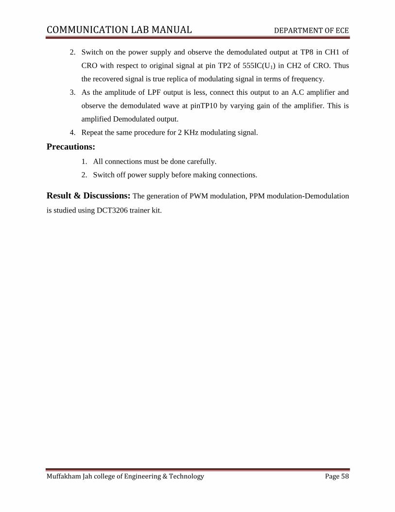
COMMUNICATION LAB MANUAL DEPARTMENT OF ECE
Muffakham Jah college of Engineering & Technology Page 58
2. Switch on the power supply and observe the demodulated output at TP8 in CH1 of
CRO with respect to original signal at pin TP2 of 555IC(U1) in CH2 of CRO. Thus
the recovered signal is true replica of modulating signal in terms of frequency.
3. As the amplitude of LPF output is less, connect this output to an A.C amplifier and
observe the demodulated wave at pinTP10 by varying gain of the amplifier. This is
amplified Demodulated output.
4. Repeat the same procedure for 2 KHz modulating signal.
Precautions:
1. All connections must be done carefully.
2. Switch off power supply before making connections.
Result & Discussions: The generation of PWM modulation, PPM modulation-Demodulation
is studied using DCT3206 trainer kit.
COMMUNICATION LAB MANUAL DEPARTMENT OF ECE
Muffakham Jah college of Engineering & Technology Page 59
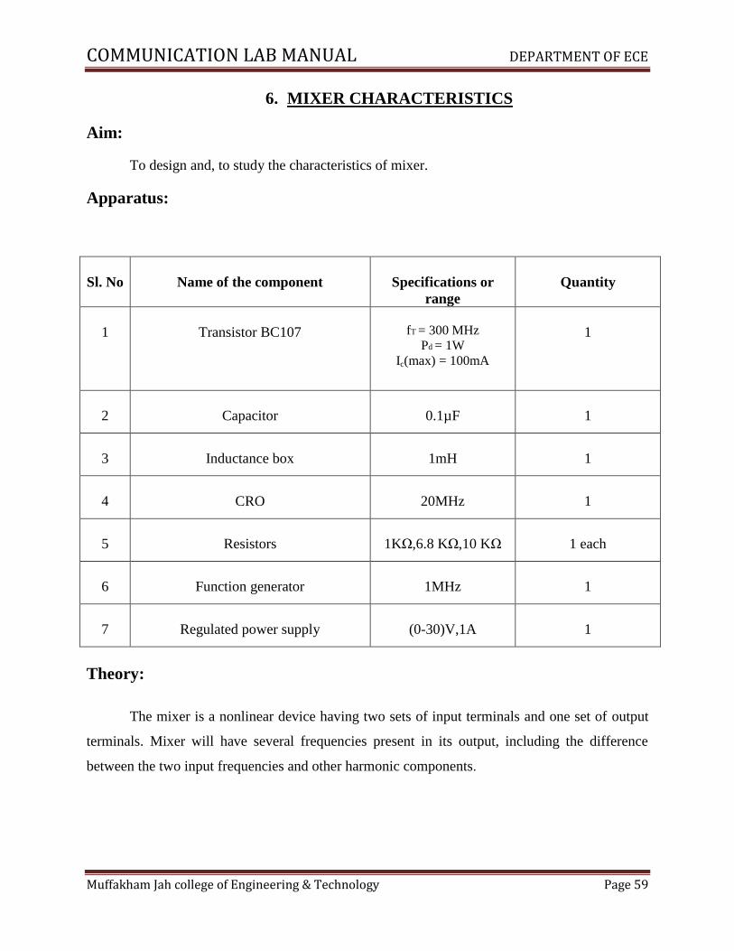
6. MIXER CHARACTERISTICS
Aim:
To design and, to study the characteristics of mixer.
Apparatus:
Sl. No
Name of the component
Specifications or
range
Quantity
1
Transistor BC107
fT = 300 MHz
Pd = 1W
Ic(max) = 100mA
1
2
Capacitor
0.1µF
1
3
Inductance box
1mH
1
4
CRO
20MHz
1
5
Resistors
1KΩ,6.8 KΩ,10 KΩ
1 each
6
Function generator
1MHz
1
7
Regulated power supply
(0-30)V,1A
1
Theory:
The mixer is a nonlinear device having two sets of input terminals and one set of output
terminals. Mixer will have several frequencies present in its output, including the difference
between the two input frequencies and other harmonic components.
COMMUNICATION LAB MANUAL DEPARTMENT OF ECE
Muffakham Jah college of Engineering & Technology Page 60
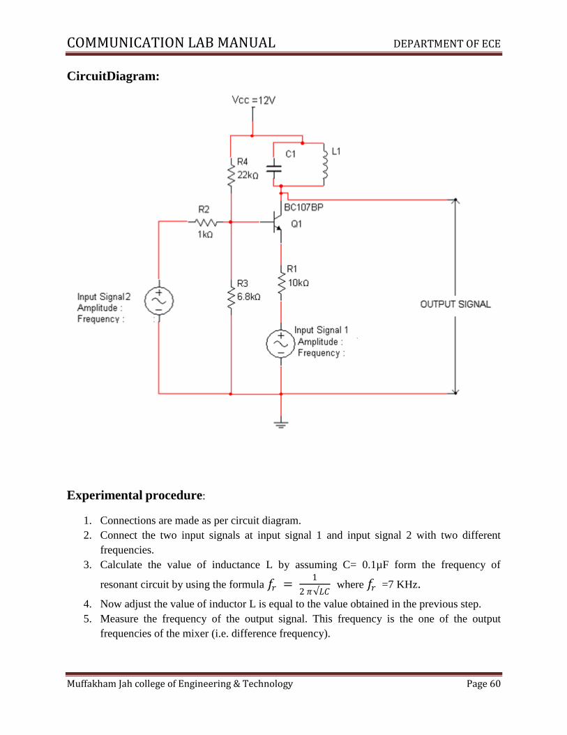
CircuitDiagram:
Experimental procedure:
1. Connections are made as per circuit diagram.
2. Connect the two input signals at input signal 1 and input signal 2 with two different
frequencies.
3. Calculate the value of inductance L by assuming C= 0.1µF form the frequency of
resonant circuit by using the formula 𝑓𝑟 = 1
2 𝜋√𝐿𝐶 where 𝑓𝑟 =7 KHz.
4. Now adjust the value of inductor L is equal to the value obtained in the previous step.
5. Measure the frequency of the output signal. This frequency is the one of the output
frequencies of the mixer (i.e. difference frequency).

COMMUNICATION LAB MANUAL DEPARTMENT OF ECE
Muffakham Jah college of Engineering & Technology Page 61
Tabular form:
Sl. No
Name of the signal
Amplitude
frequency
1 Input signal 1 4V
2 Input signal 2 4V
3 Output signal
when L=
Precautions:
1. All connections must be done carefully.
2. Switch off power supply before making connections.
Result: Thus the designing of mixer is done for the difference frequency.
COMMUNICATION LAB MANUAL DEPARTMENT OF ECE
Muffakham Jah college of Engineering & Technology Page 62
List of Experiments Page
Digital Communications
1) PCM Generation and Detection ………………………………………….…………...…...63
2) Data Formats …………………………….…….. …………………………….….………..70
3) Linear and Adaptive Delta Modulation-Demodulation...………………….….…….…….73
4) ASK Generation and Detection……………..…………………………….……………….79
5) FSK Generation and Detection …….………...….………………………..……….………83
6) .A. PSK Generation and Detection …………………..………………….………….….….88
6). B. QPSK Generation and Detection...………………………..….……….…….…..……..93

COMMUNICATION LAB MANUAL DEPARTMENT OF ECE
Muffakham Jah college of Engineering & Technology Page 63
1. PCM GENERATION AND DETECTION
Aim:
1. To study the Generation of the Pulse Code Modulation Waveform.
2. To perform Demodulation of PCM wave.
Apparatus:
Sl. No
Name of the component
Specifications or
range
Quantity
1
PCM trainer kit
-------
1
2
CRO
20MHz
1
3
Digital Multi Meter
----
1
4
Connecting wires, Probes and Patch
chords.
----
As per required
number
Theory:
Pulse Code Modulation:
Pulse Code Modulation is a Digital modulation which different from continuous
modulation schemes like Amplitude Modulation and Frequency Modulation. PCM is a technique
used to convert analog signals into binary form. In the absence of noise and distortion it is
possible to completely recover a continuous analog modulated signal at the receiving end. But in
real time they suffer from transmission distortion and noise to an appreciable extent. In the PCM
COMMUNICATION LAB MANUAL DEPARTMENT OF ECE
Muffakham Jah college of Engineering & Technology Page 64
system, groups of pulses or codes are transmitted which represent binary numbers corresponding
to modulating signal voltage levels. Recovery of the transmitter information does not depend on
the height, width, or energy content of the individual pulses, but only on their presence or
absence. Since it is relatively easy to recover pulses under these conditions, even in the presence
of large amounts of noise and distortion, PCM systems tend to be very immune to interference
and noise. Regeneration of the pulse enroute is also relatively easy, resulting in a system that
produces excellent for long- distance communication.
PCM Encoding:
The encoding process generates a binary code number corresponding to Modulating signal
voltage level to be transmitted for each sampling interval. Any one of the codes like binary,
ASCII etc, may be used as long as it provides a sufficient number of different symbols to
represent all of the levels to be transmitted. Ordinary binary number will contain a train of „1‟
and „0‟ pulses with a total of log 2n pulses in each number. (N is no of levels in the full range).
This system is very economical to realize, because it corresponds exactly to the process of
analog-to-digital (A/D) conversion.
Quantization:
The first step is in the PCM system is to quantize the modulating signal. The modulating signal
can assume an infinite number of different levels between the two limit values which define the
range of the signal in PCM. A code number is transmitted for each level sampled in the
modulating signal. If the exact number corresponding to the exact voltage were to be transmitted
for every sample, an infinitely large number of different code symbols would be needed.
Quantization has the effect of reducing this infinite number of levels to a relatively small number
which can be coded without difficulty.
In the quantization process, the total range of the modulating signal is divided up into a number
of small sub ranges. The number will depend on the nature of the modulating signal and will
form as few as 8 to as many as 128 levels. A number that is an integer power of two is generally
chosen because of the ease of generating binary codes. A new signal is generated by producing,
for each sample, a voltage level corresponding to the midpoint level of the sub range in which
the sample falls. Thus if a range of 0 to 5V were divided into 128, 5/128v sub ranges, and the
signal sampled when it was 3V, the Quantizer would put a voltage of 2.96 V and hold that level
COMMUNICATION LAB MANUAL DEPARTMENT OF ECE
Muffakham Jah college of Engineering & Technology Page 65
until the next sampling time. The result is a stepped waveform which follows the counter of the
original modulating signal with each step synchronized to the sampling period.
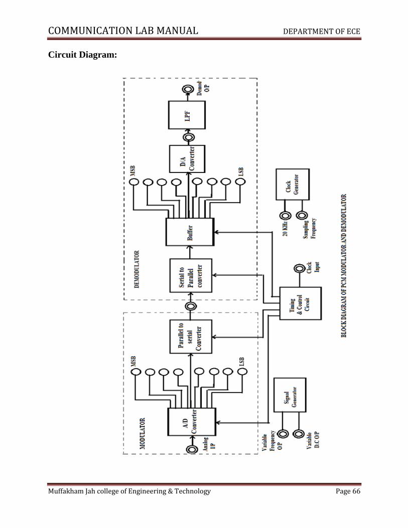
Block diagram Description:
The block diagram of PCM modulation and Demodulation is shown ion front panel given
in the circuit diagram.
Modulating signal:
A variable sinusoidal frequency generator is provided with frequency from 0 Hz to 500
Hz. To see the actual bits that are transmitted through the communication channel, a variable DC
(-5V to +5V) source is provided on the panel.
PCM Encoding:
The modulating signal is applied to the input of Analog-to-Digital Converter which
performs the two functions of Quantization and Encoding, Producing a 8-bit binary coded
number. The signal is to be transmitted i.e, modulating signal is sampled at regular intervals. If
the maximum amplitude +5V is represented by 8-bits the 1LSB corresponds to Vx1/128 =
5/128=39mV and MSB represents the sign .So the values of the sampled signal at the output of
Analog-to-Digital converter are 00000000, 00111111, 01111111, 00000000, 10111111,
11111111, 10111111, 00000000.
To transmit all the bits in one channel, actually it is often sent as binary number back to
front by parallel to serial converter. i.e, 00000001, 11111100, 11111110 to make demodulating
easier. A parallel to serial converter transmits the code bits in serial fashion.
PCM Decoding:
At the receiver end the received data will be in serial form. The serial data is converted
back to parallel form by serial to parallel converter and passes the bits to a Digital- to- Analog
converter for decoding which has in-built sample and hold amplifier which maintains the pulse
level for the duration of the sampling period, recreating the pulse level for the duration of the
sampling period, recreating the staircase waveform which is approximation of modulating signal.
A low pass filter may be used to reduce the quantization noise and to yield the original
modulating signal.
COMMUNICATION LAB MANUAL DEPARTMENT OF ECE
Muffakham Jah college of Engineering & Technology Page 66
Circuit Diagram:
COMMUNICATION LAB MANUAL DEPARTMENT OF ECE
Muffakham Jah college of Engineering & Technology Page 67
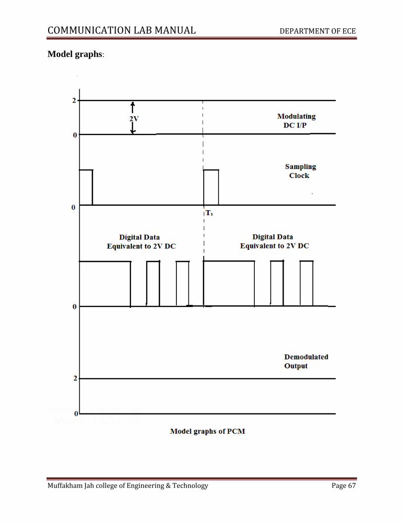
Model graphs:
COMMUNICATION LAB MANUAL DEPARTMENT OF ECE
Muffakham Jah college of Engineering & Technology Page 68
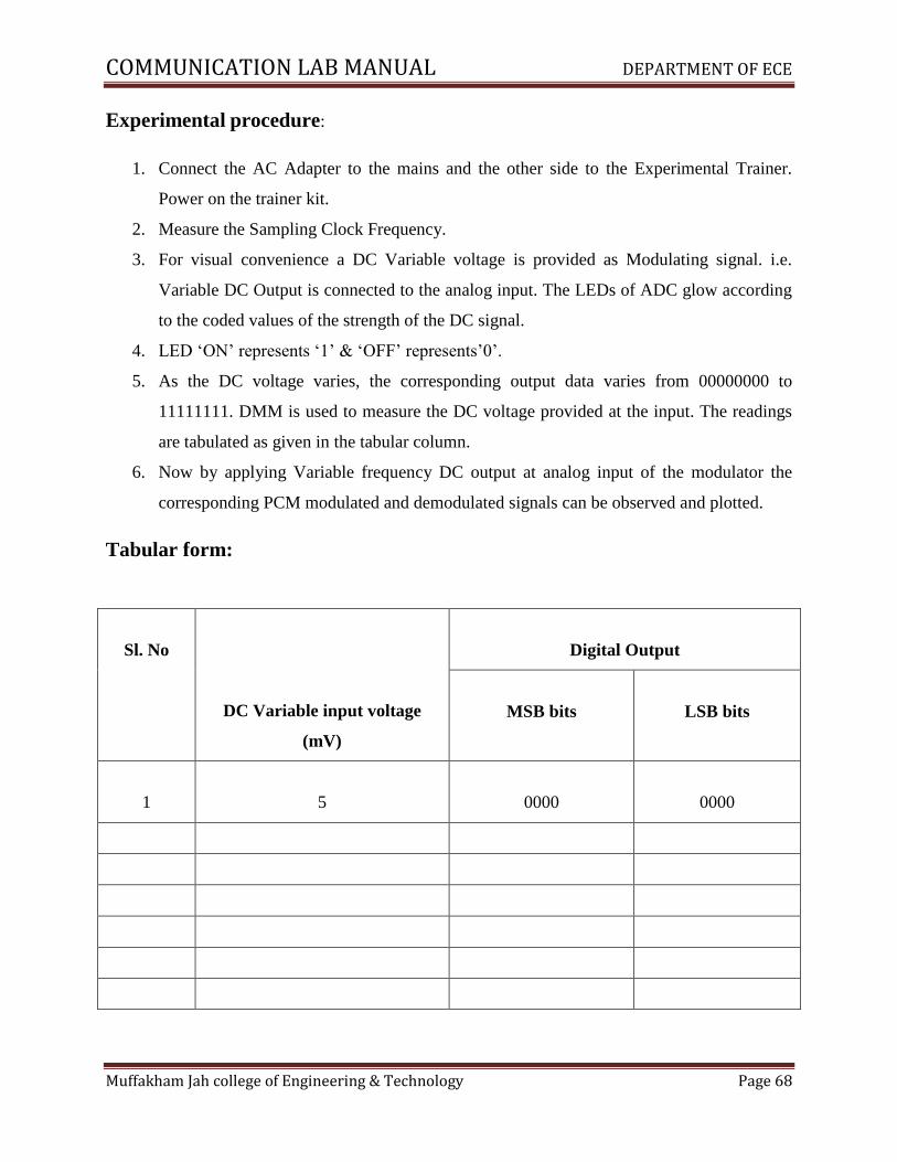
Experimental procedure:
1. Connect the AC Adapter to the mains and the other side to the Experimental Trainer.
Power on the trainer kit.
2. Measure the Sampling Clock Frequency.
3. For visual convenience a DC Variable voltage is provided as Modulating signal. i.e.
Variable DC Output is connected to the analog input. The LEDs of ADC glow according
to the coded values of the strength of the DC signal.
4. LED „ON‟ represents „1‟ & „OFF‟ represents‟0‟.
5. As the DC voltage varies, the corresponding output data varies from 00000000 to
11111111. DMM is used to measure the DC voltage provided at the input. The readings
are tabulated as given in the tabular column.
6. Now by applying Variable frequency DC output at analog input of the modulator the
corresponding PCM modulated and demodulated signals can be observed and plotted.
Tabular form:
Sl. No
DC Variable input voltage
(mV)
Digital Output
MSB bits
LSB bits
1
5
0000
0000

COMMUNICATION LAB MANUAL DEPARTMENT OF ECE
Muffakham Jah college of Engineering & Technology Page 69
Calculations:
Practical values:
Weight of LSB =
Weight of MSB =
Dynamic Range =
Theoretical values:
Weight of LSB =
Weight of MSB =
Precautions:
1. All connections must be done carefully.
2. Switch off power supply before making connections.
Result &Discussions: Thus the Pulse code modulation and demodulation is performed
practically.
COMMUNICATION LAB MANUAL DEPARTMENT OF ECE
Muffakham Jah college of Engineering & Technology Page 70
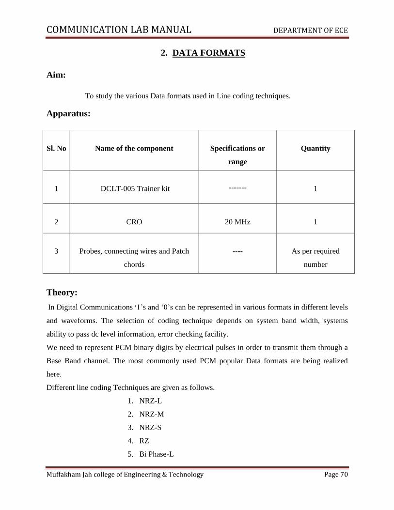
2. DATA FORMATS
Aim:
To study the various Data formats used in Line coding techniques.
Apparatus:
Sl. No
Name of the component
Specifications or
range
Quantity
1
DCLT-005 Trainer kit
-------
1
2
CRO
20 MHz
1
3
Probes, connecting wires and Patch
chords
----
As per required
number
Theory:
In Digital Communications ‘1‟s and „0‟s can be represented in various formats in different levels
and waveforms. The selection of coding technique depends on system band width, systems
ability to pass dc level information, error checking facility.
We need to represent PCM binary digits by electrical pulses in order to transmit them through a
Base Band channel. The most commonly used PCM popular Data formats are being realized
here.
Different line coding Techniques are given as follows.
1. NRZ-L
2. NRZ-M
3. NRZ-S
4. RZ
5. Bi Phase-L

COMMUNICATION LAB MANUAL DEPARTMENT OF ECE
Muffakham Jah college of Engineering & Technology Page 71
6. Bi Phase-M
7. Bi Phase-S
8. Differential Manchester.
9. RZ-AMI.
Model Graphs:
COMMUNICATION LAB MANUAL DEPARTMENT OF ECE
Muffakham Jah college of Engineering & Technology Page 72
Experimental procedure:
1. Set up the DCLT-005 in standalone mode and prepare a list of waveforms that are to be
observed in DCLT-005.
2. Connect the unit with the given power supply.
3. Connect s-clock to the Coding clock and observe the two signals.
4. Connect S-DATA to INPUT DATA and observe the two signals.
5. Connect one Channel-1 of the CRO to the S-DATA and Channel-2 to the CODED
DATA.
6. Observe CODED DATA with respect to Clock signal for various S-DATA inputs.
Precautions:
1. All connections must be done carefully.
2. Switch off power supply before making connections.
Result &Discussions: Various Data formats are observed and the waveforms are plotted.
COMMUNICATION LAB MANUAL DEPARTMENT OF ECE
Muffakham Jah college of Engineering & Technology Page 73
3. LINEAR & ADAPTIVE DELTA MODULATION AND
DEMODULATION
Aim:
To study the operation of Delta Modulation and Demodulation.
Apparatus:
Sl. No
Name of the component
Specifications or
range
Quantity
1
Delta Modulator trainer kit
-------
1
2
CRO
20MHz
1
3
Connecting wires, Probes and Patch
chords.
----
As per required
number
Theory:
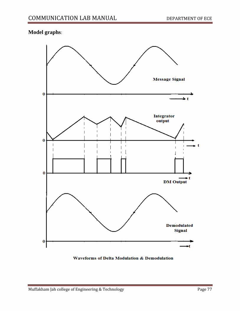
Delta Modulation & Demodulation:
PCM codes each quantized sample into a binary code that is sent and decoded at the
receiver. Another form of coded modulation is called Delta Modulation.
The main principle behind the Delta Modulation is to purposely over sampling the base
band signal purposely to increase the correlation between adjacent samples of the signal, so as to
permit the use of a sample quantizing strategy for constructing the encoded signal. Delta
Modulation is a process of converting Analog signal into one bit code. In Delta Modulation only
one bit is sent per sample. This bit indicates whether the signal is larger or smaller than the
previous samples. The advantage of Delta Modulation is that the Modulator and Demodulator
circuits are much simpler than those used in traditional PCM systems.

COMMUNICATION LAB MANUAL DEPARTMENT OF ECE
Muffakham Jah college of Engineering & Technology Page 74
The purpose behind this form of Modulation is to minimize the effects of noise without
increasing the number of bits being sent. This increases the Signal-to-Noise Ratio improving
system performance. The idea behind delta modulation is to take samples close enough to each
other so that each samples amplitude does not vary by more than signal step size. Then instead of
sending a binary code representing the step size, a single bit is sent, signifying whether the
sample size has increased or decreased by a single step.
This process can be illustrated by the following figure
The Original Signal is first transmitted and quantized as with PCM. If the sample currently being
coded is above the previous sample, then a binary bit is set to logic „1‟ .If the sample is lower
than the previous sample then the bit is set low.
COMMUNICATION LAB MANUAL DEPARTMENT OF ECE
Muffakham Jah college of Engineering & Technology Page 75
Circuit Diagram:
COMMUNICATION LAB MANUAL DEPARTMENT OF ECE
Muffakham Jah college of Engineering & Technology Page 76
COMMUNICATION LAB MANUAL DEPARTMENT OF ECE
Muffakham Jah college of Engineering & Technology Page 77
Model graphs:

COMMUNICATION LAB MANUAL DEPARTMENT OF ECE
Muffakham Jah college of Engineering & Technology Page 78
Experimental procedure:
1. Connect PLA1 to PLAA.
2. Connect Channel-1 of CRO to TPA1/TPAA. Adjust VR1 to minimum to get zero level
signal.
3. Connect Channel-1 to TP2 and Channel-2 to TPB1and adjust VR2 to obtain square wave
half the frequency of the clock rate selected (Output at TP1).
4. Connect Channel-1 to TP2 and set voltage/div of Channel 1 to mV range and observe a
triangle waveform, which is output of integrator. It can be observed that as the clock rate
is increased, amplitude of Triangle waveform decreases. This is called minimum step size
(Clock rate can be changed by depressing SW1 switch).
5. Connect Channel-1 to TPA1/TPAA; adjust VR1 in order to obtain a 1 KHz sine wave of
500 mV Pk-Pk approximately.
6. Signal approximating 1 KHz is available at the integrator output (TP2). This signal is
obtained by integrating the digital output resulting from Delta Modulation.
7. Connect Channel-1 to TP2 and Channel-2 to TPB1.It can be observed that the digital
high makes the integrator output to go upwards and digital low makes the integrator
output to go downwards.
8. With an Oscilloscope displaying three traces. It is possible to simultaneously observe the
input signal of the modulation, the digital output of the modulator and the signal is
obtained by the Integration from the modulator digital output.
9. Notice that, when the output is lower than the analog input the digital output is high,
whenever it is low when the analog input is lower than the integrated output.
10. Increase the amplitude of 1 KHz sine wave by rotating VR1 1 V and high in the next case
observe the changes in output signal. Repeat the same for different signal sources.
Precautions:
1. All connections must be done carefully.
2. Switch off power supply before making connections.
Result &Discussions: Thus the Delta modulation and demodulation is performed practically
and the waveforms are plotted.

COMMUNICATION LAB MANUAL DEPARTMENT OF ECE
Muffakham Jah college of Engineering & Technology Page 79
4. ASK GENERATION & DETECTION
Aim:
To generate ASK Modulated wave and To Demodulate the ASK signal.
Apparatus:
Sl. No
Name of the component
Specifications or
range
Quantity
1
ASK trainer kit
-------
1
2
CRO
20MHz
1
3
Connecting wires, Probes and Patch
chords.
----
As per required
number
Theory:
Amplitude Shift Keying:
When it is required to transmit digital signals of the sinusoidal carrier is varied in
accordance with the incoming digital data since the digital data is in discrete steps, the
modulation of band pass sinusoidal carrier is also done in discrete steps. Therefore, this type of
modulation is called switching or signaling. If the amplitude of the carrier is switched depending
on the incoming digital signal then it is called amplitude shift keying (ASK). This is similar to
analog amplitude modulation.Amplitude shift keying (ASK) or ON-OFF keying is the simplest
digital modulation technique. In this method, there is only one unit energy carrier and sit is
switched on (or) off depending upon the input binary sequence. The ASK waveform can
represented as S(t) = 2Ps cos (2fot), (to transmit „1‟). To transmit symbol „0‟, the signal s(t)
= 0 where Ps is power dissipated and fo is carrier frequency. The Original Signal is first
transmitted and quantized as with PCM. If the sample currently being coded is above the
previous sample, then a binary bit is set to logic „1‟ .If the sample is lower than the previous
sample then the bit is set low.
COMMUNICATION LAB MANUAL DEPARTMENT OF ECE
Muffakham Jah college of Engineering & Technology Page 80
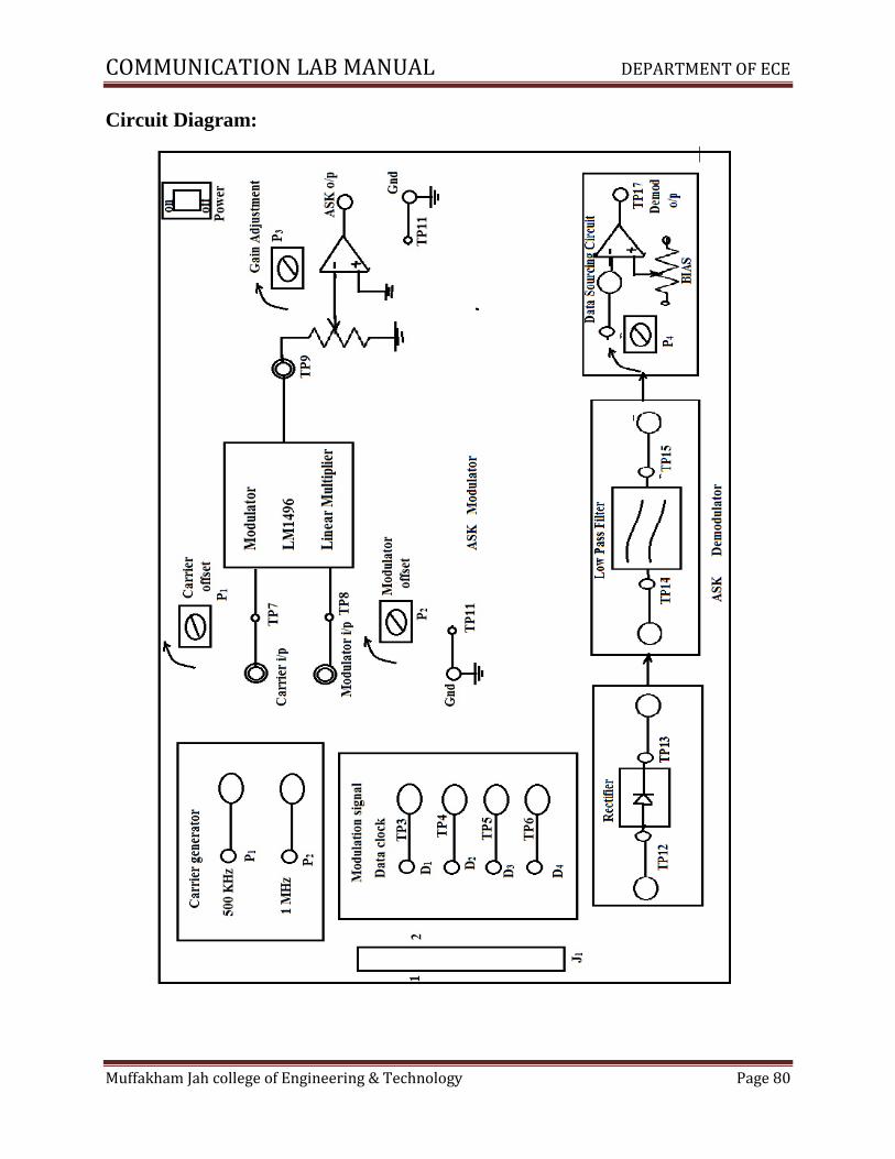
Circuit Diagram:
COMMUNICATION LAB MANUAL DEPARTMENT OF ECE
Muffakham Jah college of Engineering & Technology Page 81
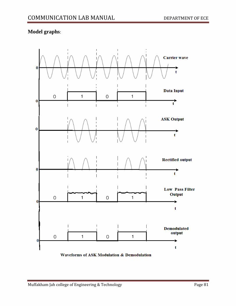
Model graphs:
COMMUNICATION LAB MANUAL DEPARTMENT OF ECE
Muffakham Jah college of Engineering & Technology Page 82
Experimental procedure:
Modulation:
1. Switch on the power supply.
2. The carrier frequency (sinusoid) is selected at carrier generation and is given to carrier
input TPL1.
3. The data clock duty cycle is adjusted by the potentiometer P1 and is given to the
modulation input at TP5. The data clock at TP6 is observed and connected to TP5.
4. By applying carrier input and digital system stream input to the double balanced
modulation the output ASK waveform is observed.
5. The ASK output can be adjusted by the gain adjustment potentiometer TP5.
Demodulation:
1. The ASK input is given to the input of rectifier.
2. This rectified signal is passed through low pass filter to remove carrier wave.
3. This out coming waveform is given to the data squaring circuit which sets up a threshold.
If the input to this circuit is greater than threshold it is set as +5V otherwise 0V.
4. The demodulated output at TP1 8 is observed.
Precautions:
1. All connections must be done carefully.
2. Switch off power supply before making connections.
Result &Discussions: Thus the ASK modulation and demodulation is performed practically
and the waveforms are plotted.
COMMUNICATION LAB MANUAL DEPARTMENT OF ECE
Muffakham Jah college of Engineering & Technology Page 83
5. FSK GENERATION AND DETECTION
Aim:
1. To generate FSK modulated wave.
2. To generate Demodulated FSK signal.
3. To generate the NRZ-L signal.
Apparatus:
Sl. No
Name of the component
Specifications or
range
Quantity
1
FSK trainer kit
-------
1
2
CRO
20MHz
1
3
Connecting wires, Probes and Patch
chords.
----
As per required
number
Theory:
Frequency Shift Keying:
When a digital signal is to be transmitted over a long distance, it needs continuous wave
modulation.
A carrier of frequency „fo‟ is used for modulation. Then the digital signal modulates some
parameter like frequency, phase or amplitude of the carrier. The carrier „fo‟ has some deviation
in frequency. The deviation is called bandwidth of the channel. Thus the channel has to transmit
some range of frequency. Hence such a type of transmission is called band pass transmission
and the communication channel is called band pass channel.
When it is required to transmit digital signals on band pass channel the amplitude, frequency (or)
phase of the sinusoidal carrier is varied in accordance with the incoming digital data. Since the
COMMUNICATION LAB MANUAL DEPARTMENT OF ECE
Muffakham Jah college of Engineering & Technology Page 84
digital data is in discrete steps, the modulation of band pass sinusoidal carrier is also done in
discrete steps. Hence this type of modulation is called switching or signaling. If the frequency
of the sinusoidal carrier is switched on depending on the incoming digital signal, then it is called
frequency shift keying (FSK). This is similar to analog frequency modulation.
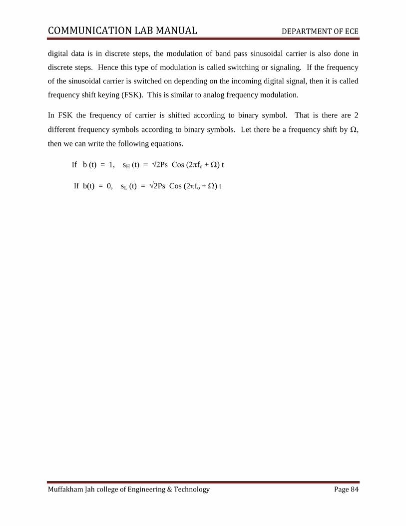
In FSK the frequency of carrier is shifted according to binary symbol. That is there are 2
different frequency symbols according to binary symbols. Let there be a frequency shift by ,
then we can write the following equations.
If b (t) = 1, sH (t) = √2Ps Cos (2fo + ) t
If b(t) = 0, sL (t) = 2Ps Cos (2fo + ) t
COMMUNICATION LAB MANUAL DEPARTMENT OF ECE
Muffakham Jah college of Engineering & Technology Page 85
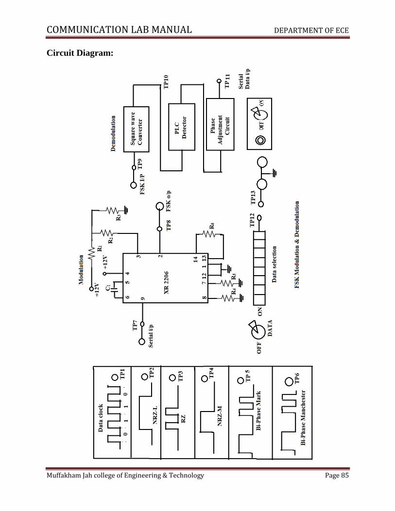
Circuit Diagram:
COMMUNICATION LAB MANUAL DEPARTMENT OF ECE
Muffakham Jah college of Engineering & Technology Page 86
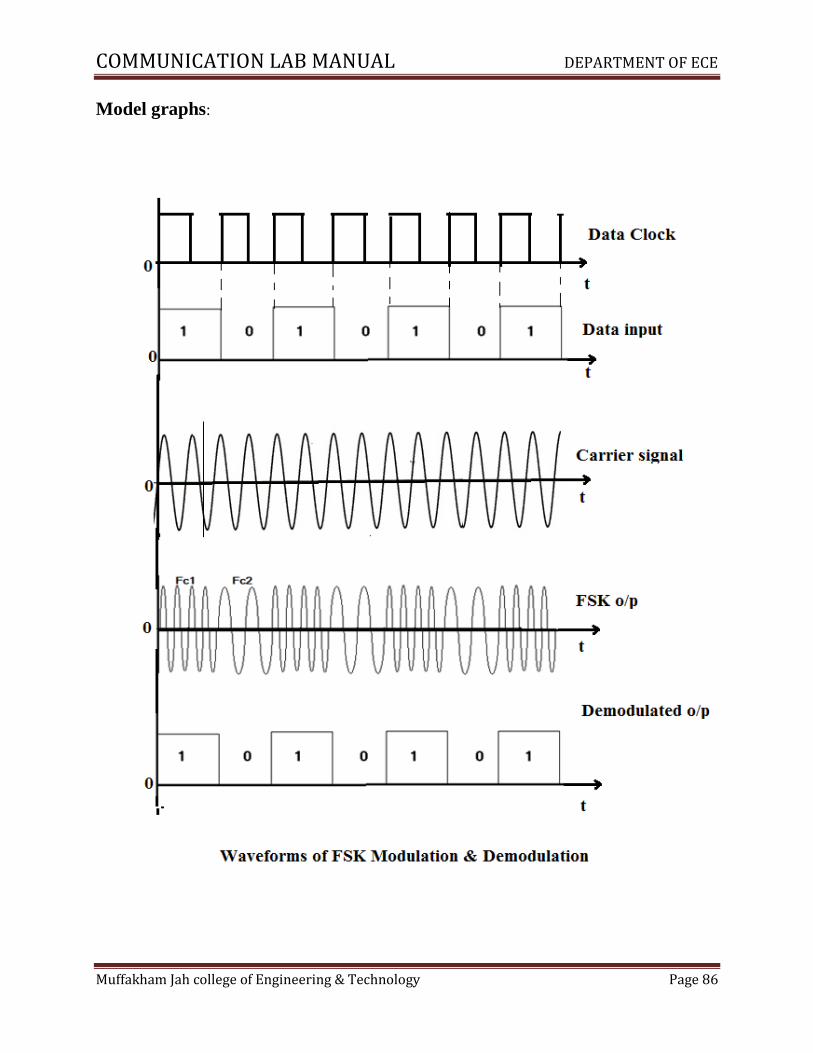
Model graphs:

COMMUNICATION LAB MANUAL DEPARTMENT OF ECE
Muffakham Jah college of Engineering & Technology Page 87
Experimental procedure:
Modulation:
1. The power supply is switched ON and data selection switch is set to the desired code.
2. The switch is set (DATA ON-OFF) ON position. The 8 bit word pattern is observed on
TP12.
3. Observe the data clock at TP1 and also observe NRZ (l) at TP2, RZ at TP3, and NRZ (M)
at TP4.
4. The patch cords are connected. The corresponding output (when data is logic „1‟
frequency is high) at TP8.
5. Repeat the steps for other inputs and observe the corresponding FSK outputs.
6. The data selections are changed and repeat the steps 3 to 6 & observe corresponding FSK
outputs.
Demodulation:
1. The patch chords are connected. The incoming FSK input is observed.
2. The output of square wave converter is available at TO10. The serial output data is
available at TP11.
3. Repeat steps 1, 2 for other serial data inputs and outputs and the corresponding serial data
is observed. The outputs are replica of the original inputs.
Precautions:
1. All connections must be done carefully.
2. Switch off power supply before making connections.
Result &Discussions: Thus the FSK modulation and demodulation is performed practically
and the waveforms are plotted.
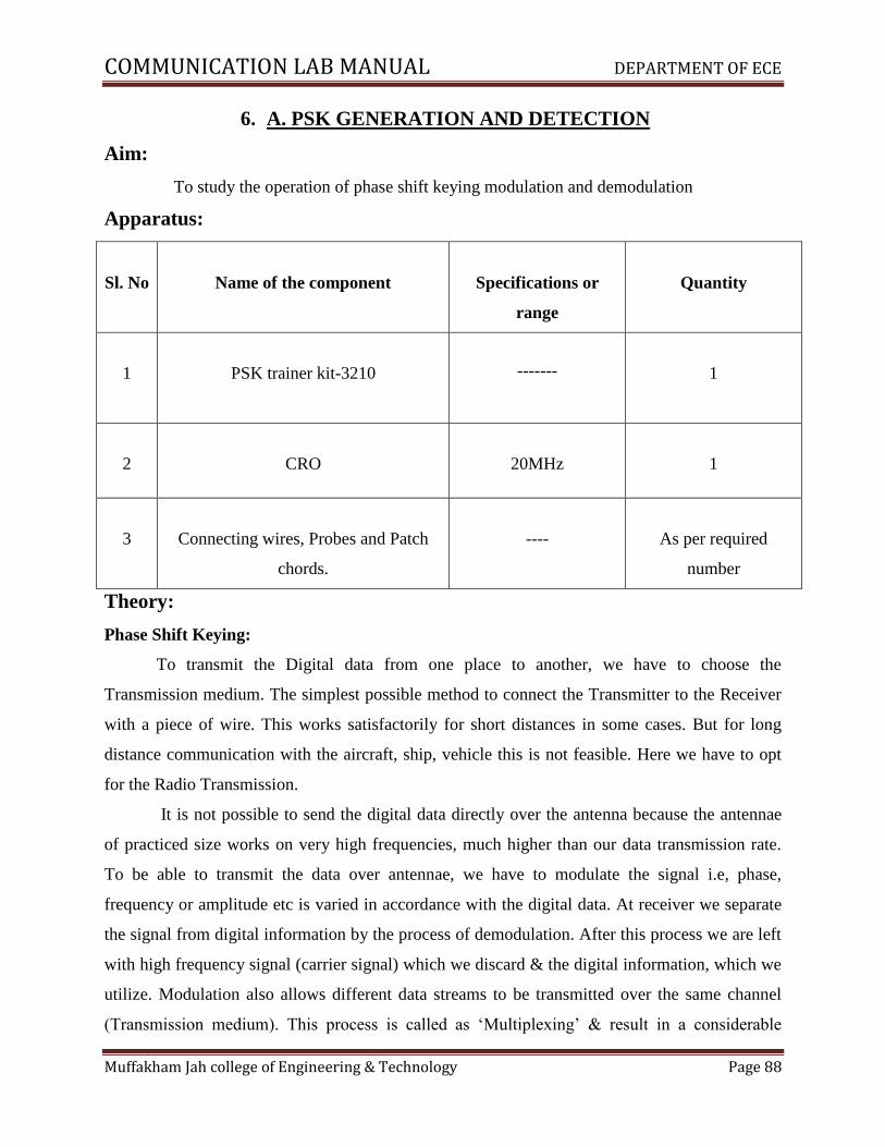
COMMUNICATION LAB MANUAL DEPARTMENT OF ECE
Muffakham Jah college of Engineering & Technology Page 88
6. A. PSK GENERATION AND DETECTION
Aim:
To study the operation of phase shift keying modulation and demodulation
Apparatus:
Sl. No
Name of the component
Specifications or
range
Quantity
1
PSK trainer kit-3210
-------
1
2
CRO
20MHz
1
3
Connecting wires, Probes and Patch
chords.
----
As per required
number
Theory:
Phase Shift Keying:
To transmit the Digital data from one place to another, we have to choose the
Transmission medium. The simplest possible method to connect the Transmitter to the Receiver
with a piece of wire. This works satisfactorily for short distances in some cases. But for long
distance communication with the aircraft, ship, vehicle this is not feasible. Here we have to opt
for the Radio Transmission.
It is not possible to send the digital data directly over the antenna because the antennae
of practiced size works on very high frequencies, much higher than our data transmission rate.
To be able to transmit the data over antennae, we have to modulate the signal i.e, phase,
frequency or amplitude etc is varied in accordance with the digital data. At receiver we separate
the signal from digital information by the process of demodulation. After this process we are left
with high frequency signal (carrier signal) which we discard & the digital information, which we
utilize. Modulation also allows different data streams to be transmitted over the same channel
(Transmission medium). This process is called as „Multiplexing‟ & result in a considerable

COMMUNICATION LAB MANUAL DEPARTMENT OF ECE
Muffakham Jah college of Engineering & Technology Page 89
saving in Bandwidth no of channels to be used, Also it increases the channel efficiency. As
variation of particular parameter variation of the carrier wave give rise to various modulation
techniques. Some of the basic modulation techniques are ASK, FSK, PSK, DPSK &QPSK.
PSK is a form of angle modulated, constant amplitude digital modulation. Digital
communication become important with the expansion of the use of computers and data
processing and have continued to develop into a major industry providing the interconnection of
computer peripherals and transmission of data between distant sites.
PSK is a relatively new system in which the carrier may have phase which is fixed for
one level and is shifted by 1800 for another level. PSK is similar to PSK in many aspects, as in
PSK, frequency of carrier is shifted according to the modulating square wave.
Circuit Description:
In this trainer IC XR 2206 is a basic wave form generator which generates Sine, Square,
and Triangle Waveforms. The sine wave generated by this XR 2206 IC is used as carrier signal
to the system. This square wave is used as a clock input to a decade counter (IC 7490) which
generates the modulating data outputs. The digital signal is applied to the modulation input for
PSK generation is bipolar i.e., have equal positive and negative voltage levels. When the
modulating input is negative the output of the modulator is a sine wave in phase with the carrier
input. Whereas for the positive voltage levels, the modulator is a sine wave which is shifted out
of phase by 180o from the carrier input compared to the differential data stream. This happens
because the carrier input is now multiplied by the negative constant level. +Thus the output
changes in phase when a change in polarity of the modulating signal results. The functional
blocks of the PSK Modulator & Demodulator.
Modulation:
IC CD 4051 is an Analog multiplexer to which carrier is applied with and without 180o
phase shift to the two multiplex inputs of the IC. Modulating data input is applied to its control
input. Depending up on the level of the controlling signal, carrier signal applied with or without
phase shift is steered to the output. The 180o phase shift to the carrier signal is carried by an
operational amplifier using 741 IC.
Demodulation:
During the demodulation the PSK signal is converted into a +5 volts Square wave signal
using a transistor and is applied to one input of an EX-OR gate. To the second input of the gate
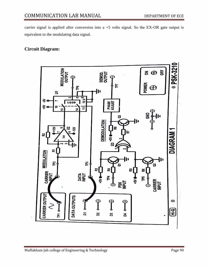
COMMUNICATION LAB MANUAL DEPARTMENT OF ECE
Muffakham Jah college of Engineering & Technology Page 90
carrier signal is applied after conversion into a +5 volts signal. So the EX-OR gate output is
equivalent to the modulating data signal.
Circuit Diagram:
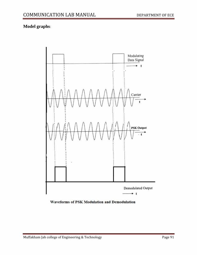
COMMUNICATION LAB MANUAL DEPARTMENT OF ECE
Muffakham Jah college of Engineering & Technology Page 91
Model graphs:

COMMUNICATION LAB MANUAL DEPARTMENT OF ECE
Muffakham Jah college of Engineering & Technology Page 92
Experimental procedure:
Modulation:
1. The trainer is switched ON. The carrier signal is observed at TP1.
2. Data outputs (D1, D2, D3, and D4) are observed.
3. Carrier output TP1 is connected to carrier input of PSK modulator at TP2 using patch
chord.
4. Connect data input „D1‟ to input of PSK modulator at TP3. The PSK output waveform is
observed on CRO on channel – 1 & corresponding data input on channel – 2.
5. These steps are repeated for D2, D3 & D4 and the corresponding PSK output are observed.
Demodulation:
1. Connect the PSK modulation output TP6 to the PSK input of Demodulator at TP4.
2. Connect carrier output TP1 to the carrier input of PSK modulator at TP5.
3. Observe the PSK modulated output at TP7 on CRO at Channel-1 and corresponding data
output on channel-2.
4. The demodulated output is true replica of data outputs D2, D3, and D4.
Precautions:
1. All connections must be done carefully.
2. Switch off power supply before making connections.
Result &Discussions: Thus the PSK modulation and demodulation is performed practically
and the waveforms are plotted.

COMMUNICATION LAB MANUAL DEPARTMENT OF ECE
Muffakham Jah college of Engineering & Technology Page 93
6. B. QPSK GENERATION AND DETECTION
Aim:
To study the operation of Quadrature phase shift keying modulation and to plot
QPSK modulated wave.
Apparatus:
Sl. No
Name of the component
Specifications or
range
Quantity
1
Physitech QPSK trainer kit
-------
1
2
CRO
20MHz
1
3
Connecting wires, Probes and Patch
chords.
----
As per required
number
Theory:
QPSK Modulation:
In QPSK, the phase of the carrier depends upon the pair of successive bits in the data stream.
This there are four possible combinations of bit pair viz 00, 01, 10 & 11. During each
combination of bit pair, the carrier frequency fc is transmitted with Quadrature phase difference.
Bit Pair Phase of
Carrier
00 fc <00
01 fc <1800
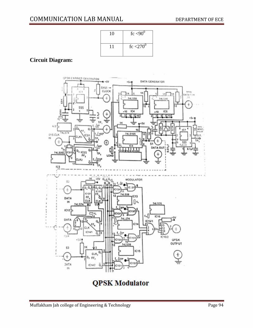
COMMUNICATION LAB MANUAL DEPARTMENT OF ECE
Muffakham Jah college of Engineering & Technology Page 94
10 fc <900
11 fc <2700
Circuit Diagram:
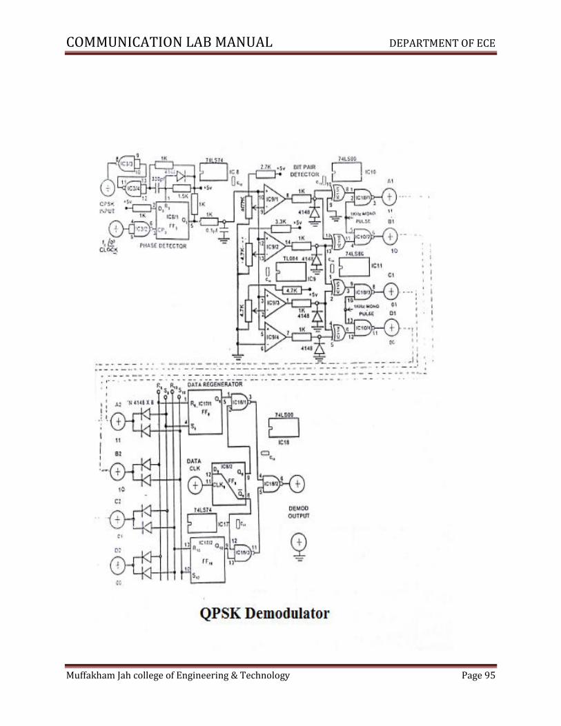
COMMUNICATION LAB MANUAL DEPARTMENT OF ECE
Muffakham Jah college of Engineering & Technology Page 95
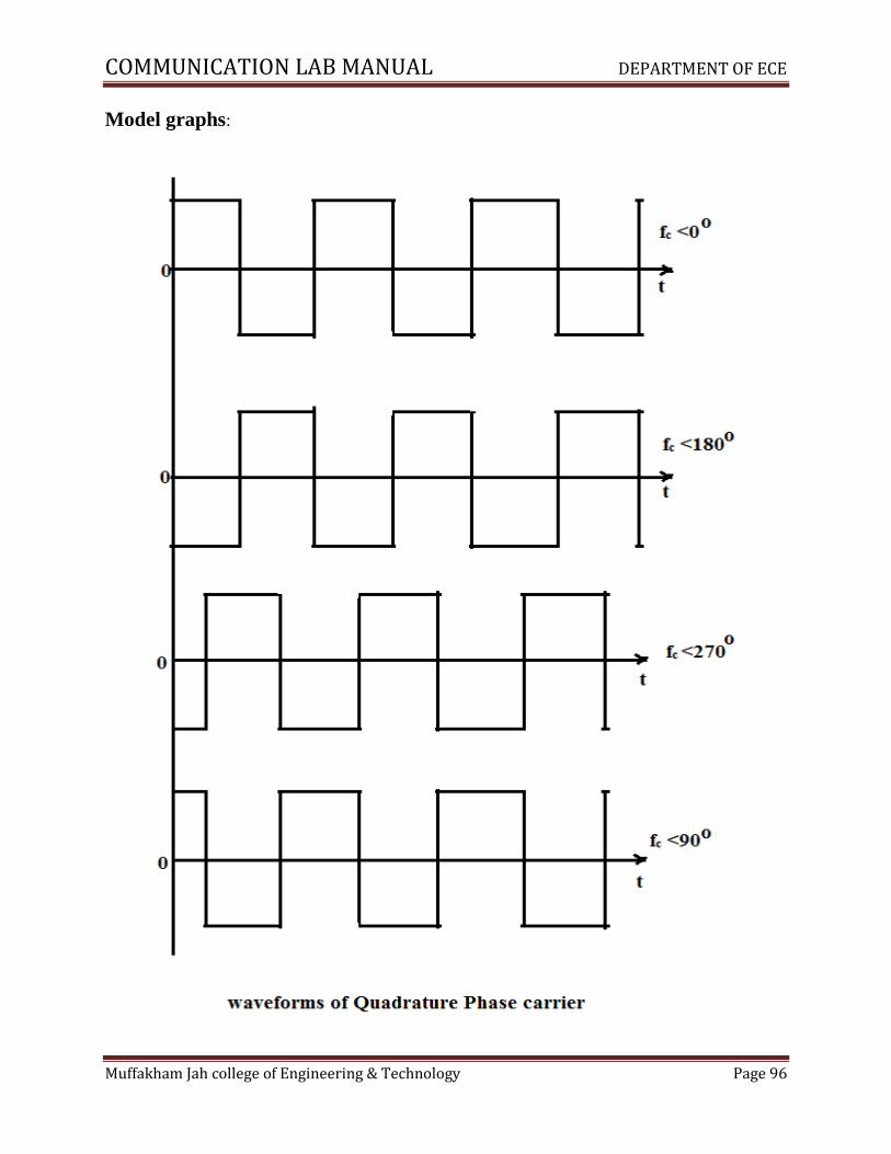
COMMUNICATION LAB MANUAL DEPARTMENT OF ECE
Muffakham Jah college of Engineering & Technology Page 96
Model graphs:
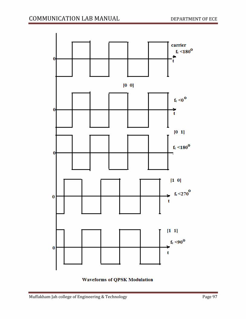
COMMUNICATION LAB MANUAL DEPARTMENT OF ECE
Muffakham Jah college of Engineering & Technology Page 97
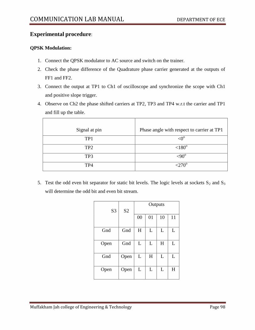
COMMUNICATION LAB MANUAL DEPARTMENT OF ECE
Muffakham Jah college of Engineering & Technology Page 98
Experimental procedure:
QPSK Modulation:
1. Connect the QPSK modulator to AC source and switch on the trainer.
2. Check the phase difference of the Quadrature phase carrier generated at the outputs of
FF1 and FF2.
3. Connect the output at TP1 to Ch1 of oscilloscope and synchronize the scope with Ch1
and positive slope trigger.
4. Observe on Ch2 the phase shifted carriers at TP2, TP3 and TP4 w.r.t the carrier and TP1
and fill up the table.
Signal at pin
Phase angle with respect to carrier at TP1
TP1 <0o
TP2 <180o
TP3 <90o
TP4 <270o
5. Test the odd even bit separator for static bit levels. The logic levels at sockets S2 and S3
will determine the odd bit and even bit stream.
S3 S2
Outputs
00 01 10 11
Gnd Gnd H L L L
Open Gnd L L H L
Gnd Open L H L L
Open Open L L L H

COMMUNICATION LAB MANUAL DEPARTMENT OF ECE
Muffakham Jah college of Engineering & Technology Page 99
6. Test the selection of carrier w.r.t the bit pattern generation. Observe on Channel-1 carrier
fc <180o at TP1. Connect on Channel-2, the output of QPSK modulator. Observe the
switched carrier as
Socket
S2
Socket
S3
Phase angle of
QPSK O/P w.r.t
fc <180o carrier
Gnd (0) Gnd (0) fc <00
Open (1) Gnd (0) fc <900
Gnd (0) Open (1) fc <1800
Open (1) Open (1) fc <2700
Precautions:
1. All connections must be done carefully.
2. Switch off power supply before making connections.
Result &Discussions: Thus QPSK modulation and demodulation is performed practically
and graphs are plotted.

COMMUNICATION LAB MANUAL DEPARTMENT OF ECE
Muffakham Jah college of Engineering & Technology Page 100
List of Experiments Page
Communication Lab Using MATLAB
1) Generation & Detection of Analog and Pulse Modulation techniques using MATLAB…...101
2) Generation & Detection of Analog and Digital Modulation schemes using MATLAB.…...110

COMMUNICATION LAB MANUAL DEPARTMENT OF ECE
Muffakham Jah college of Engineering & Technology Page 101
1. GENERATION & DETECTION OF ANALOG AND PULSE MODULATION
TECHNIQUES BY USING MATLAB
Aim:
To Generate & to detect analog Modulation schemes like AM, FM and Pulse Modulation
techniques like PAM, PWM and PPM using MATLAB.
Software required: MATLAB2010a
Program:
1. Amplitude Modulation:
clc;
clear all;
close all;
t=linspace(0,0.1,50000); %defining time range
for the signal
fc=1000; %frequency of carrier signal
fm=500; %frequency of message signal
fs=100000;%samplingfrequency---fs>=2(fc+BW)
Am=5; %amplitude of the message signal
Ac=10; %amplitude of the carrier signal
m=Am/Ac %modulation index for the AM wave
wc=2*pi*fc*t; %carrier frequency in radians
wm=2*pi*fm*t; %message frequency in radians
ec=Ac*sin(wc); %carrier signal
em=Am*sin(wm); %message signal
y=ammod(em,fc,fs,0,Ac); %AM signal
z=amdemod(y,fc,fs,0,Ac);%demodulated AM
signal
l=50000;
subplot(4,1,1),plot(t(1:l),em(1:l))
xlabel('time(sec)');
ylabel('amplitude in volts(V)');
title('MODULATING SIGNAL');
subplot(4,1,2),plot(t(1:l/2),ec(1:l/2))
xlabel('time(sec)');
ylabel('amplitude in volts(V)');
title('CARRIER SIGNAL');
subplot(4,1,3),plot(t(1:l),y(1:l))
axis([0 0.02 -20 20]) %setting axis dimensions
xlabel('time(sec)');
ylabel('amplitude in volts(V)');
title('AMPLITUDE MODULATED SIGNAL');
subplot(4,1,4),plot(t(1:l),z(1:l))
xlabel('time(sec)');
ylabel('amplitude in volts(V)');
title(' AM DEMODULATED SIGNAL');
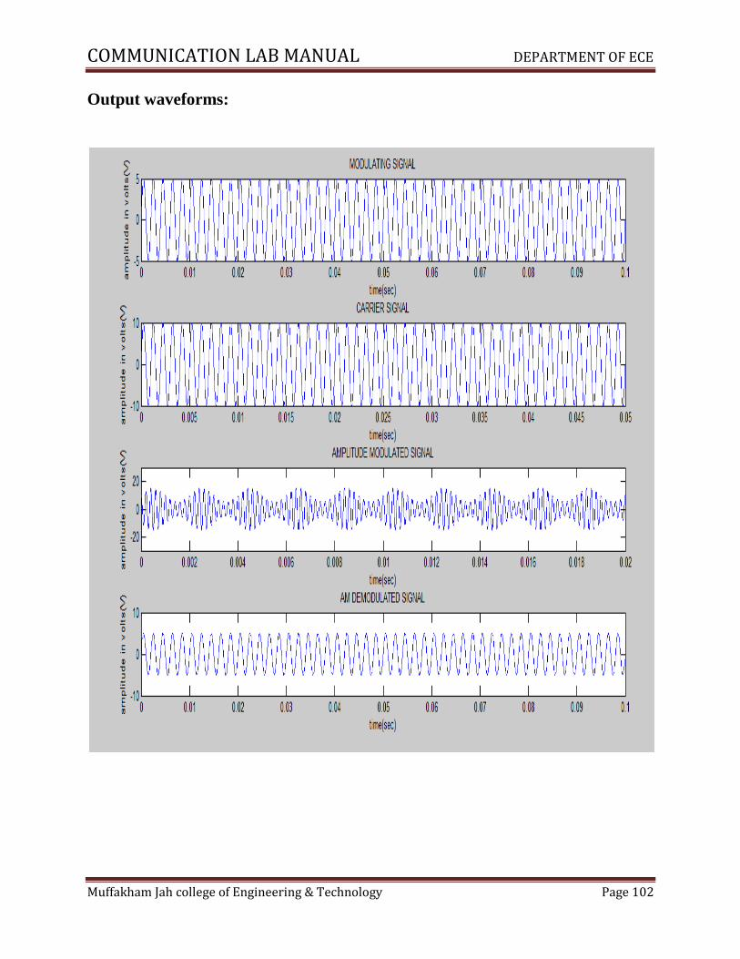
COMMUNICATION LAB MANUAL DEPARTMENT OF ECE
Muffakham Jah college of Engineering & Technology Page 102
Output waveforms:

COMMUNICATION LAB MANUAL DEPARTMENT OF ECE
Muffakham Jah college of Engineering & Technology Page 103
2. Frequency Modulation:
clc
clear all
close all
Fs = 8000; % Sampling rate of signal
Fc = 100; % Carrier frequency
t = linspace(0,1,10000); % Sampling times
x = sin(2*pi*10*t) % Channel 1
dev = 75; % Frequency deviation in modulated signal
y = fmmod(x,Fc,Fs,dev); % Modulate both channels.
z = fmdemod(y,Fc,Fs,dev); % Demodulate both channels.
subplot(411),plot(t,x)
xlabel('time(sec)');
ylabel('amplitude in volts(V)');
title('MODULATING SIGNAL');
subplot(412),plot(t,sin(2*pi*Fc*t))
xlabel('time(sec)');
ylabel('amplitude in volts(V)');
title('CARRIER SIGNAL');
subplot(413),plot(t,y)
xlabel('time(sec)');
ylabel('amplitude in volts(V)');
title('FREQUENCY MODULATED SIGNAL');
subplot(414),plot(t,z)
xlabel('time(sec)');
ylabel('amplitude in volts(V)');
title(' FM DEMODULATED SIGNAL');
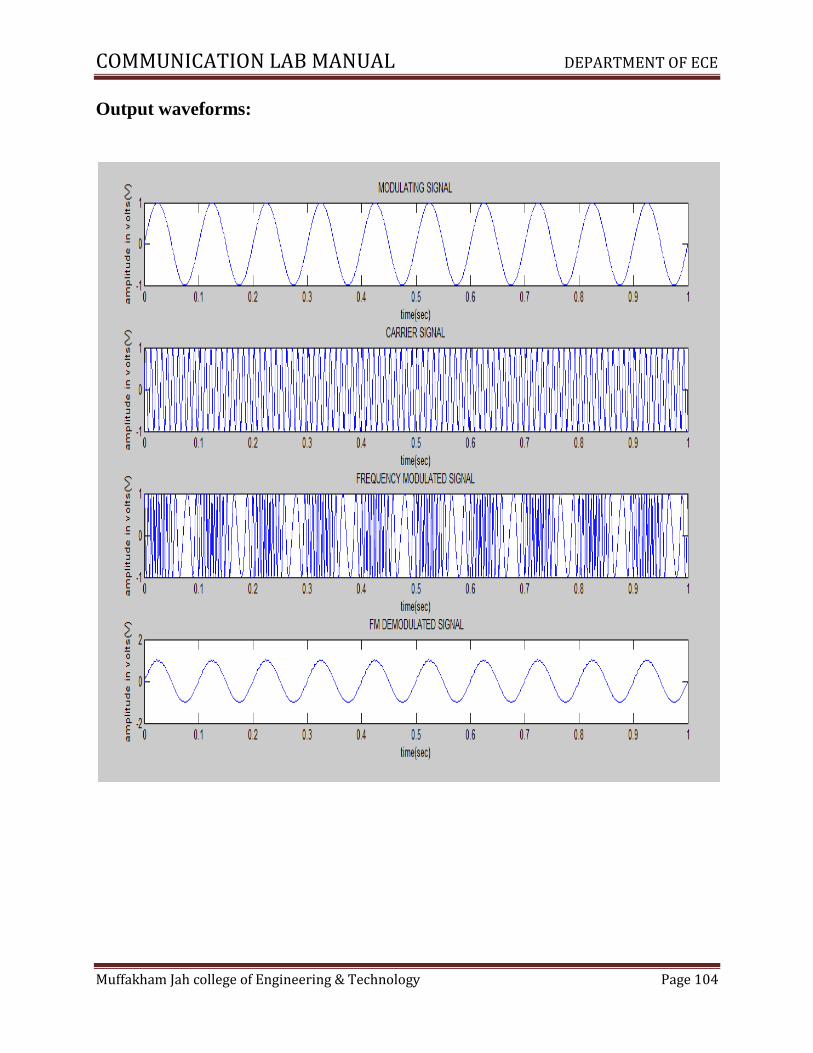
COMMUNICATION LAB MANUAL DEPARTMENT OF ECE
Muffakham Jah college of Engineering & Technology Page 104
Output waveforms:

COMMUNICATION LAB MANUAL DEPARTMENT OF ECE
Muffakham Jah college of Engineering & Technology Page 105
3. Pulse Width Modulation:
%PWM wave generation without functions
clc;
clear all;
close all;
t=0:0.001:2;
s=sawtooth(2*pi*20*t+pi);
m=0.75*sin(2*pi*1*t);
n=length(s);
for i=1:n
if (m(i)>=s(i))
pwm(i)=0;
elseif (m(i)<=s(i))
pwm(i)=1;
end
end
subplot(211),plot(t,m,'-r',t,s,'-b');axis([0 2 -1.5
1.5]);
title('message signal with sawtooth
comparison')
xlabel('time(sec)');
ylabel('voltage(V)');
subplot(212),plot(t,pwm,'-k')
axis([0 2 -0.5 1.5]);
title('PWM wave');
xlabel('time(sec)');
ylabel('voltage(V)');
Output waveforms:
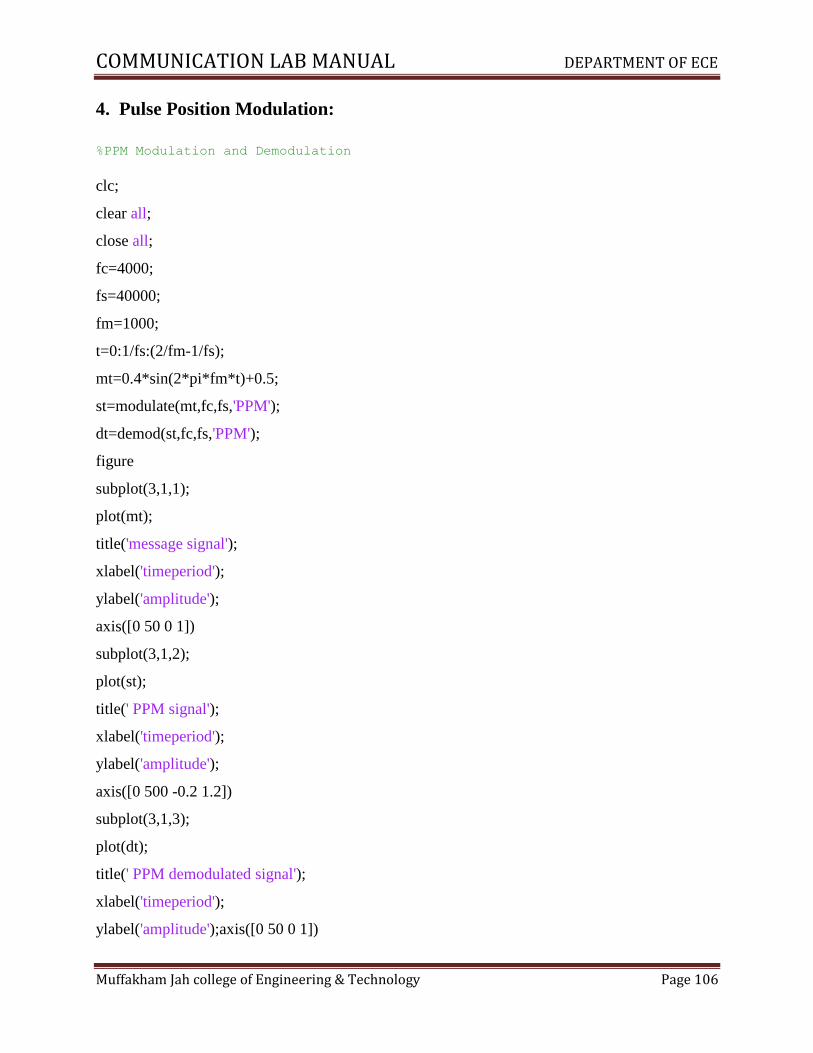
COMMUNICATION LAB MANUAL DEPARTMENT OF ECE
Muffakham Jah college of Engineering & Technology Page 106
4. Pulse Position Modulation:
%PPM Modulation and Demodulation
clc;
clear all;
close all;
fc=4000;
fs=40000;
fm=1000;
t=0:1/fs:(2/fm-1/fs);
mt=0.4*sin(2*pi*fm*t)+0.5;
st=modulate(mt,fc,fs,'PPM');
dt=demod(st,fc,fs,'PPM');
figure
subplot(3,1,1);
plot(mt);
title('message signal');
xlabel('timeperiod');
ylabel('amplitude');
axis([0 50 0 1])
subplot(3,1,2);
plot(st);
title(' PPM signal');
xlabel('timeperiod');
ylabel('amplitude');
axis([0 500 -0.2 1.2])
subplot(3,1,3);
plot(dt);
title(' PPM demodulated signal');
xlabel('timeperiod');
ylabel('amplitude');axis([0 50 0 1])
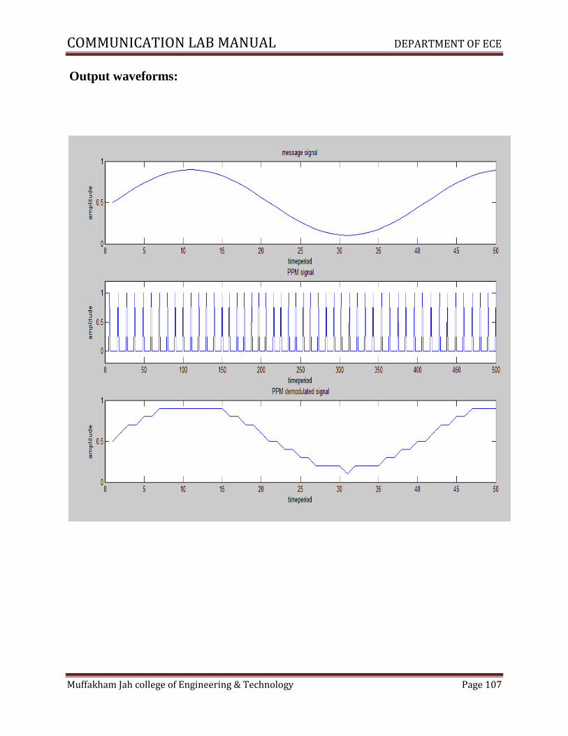
COMMUNICATION LAB MANUAL DEPARTMENT OF ECE
Muffakham Jah college of Engineering & Technology Page 107
Output waveforms:
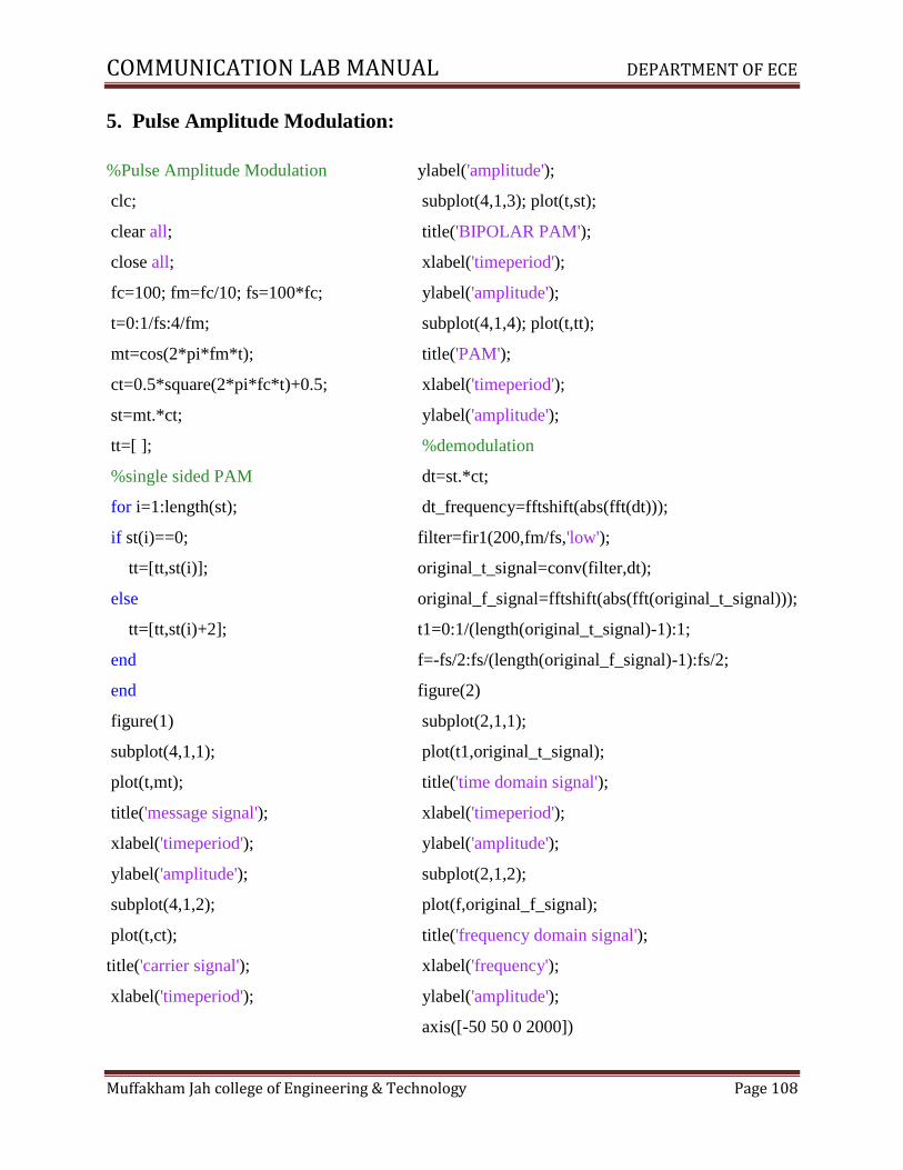
COMMUNICATION LAB MANUAL DEPARTMENT OF ECE
Muffakham Jah college of Engineering & Technology Page 108
5. Pulse Amplitude Modulation:
%Pulse Amplitude Modulation
clc;
clear all;
close all;
fc=100; fm=fc/10; fs=100*fc;
t=0:1/fs:4/fm;
mt=cos(2*pi*fm*t);
ct=0.5*square(2*pi*fc*t)+0.5;
st=mt.*ct;
tt=[ ];
%single sided PAM
for i=1:length(st);
if st(i)==0;
tt=[tt,st(i)];
else
tt=[tt,st(i)+2];
end
end
figure(1)
subplot(4,1,1);
plot(t,mt);
title('message signal');
xlabel('timeperiod');
ylabel('amplitude');
subplot(4,1,2);
plot(t,ct);
title('carrier signal');
xlabel('timeperiod');
ylabel('amplitude');
subplot(4,1,3); plot(t,st);
title('BIPOLAR PAM');
xlabel('timeperiod');
ylabel('amplitude');
subplot(4,1,4); plot(t,tt);
title('PAM');
xlabel('timeperiod');
ylabel('amplitude');
%demodulation
dt=st.*ct;
dt_frequency=fftshift(abs(fft(dt)));
filter=fir1(200,fm/fs,'low');
original_t_signal=conv(filter,dt);
original_f_signal=fftshift(abs(fft(original_t_signal)));
t1=0:1/(length(original_t_signal)-1):1;
f=-fs/2:fs/(length(original_f_signal)-1):fs/2;
figure(2)
subplot(2,1,1);
plot(t1,original_t_signal);
title('time domain signal');
xlabel('timeperiod');
ylabel('amplitude');
subplot(2,1,2);
plot(f,original_f_signal);
title('frequency domain signal');
xlabel('frequency');
ylabel('amplitude');
axis([-50 50 0 2000])
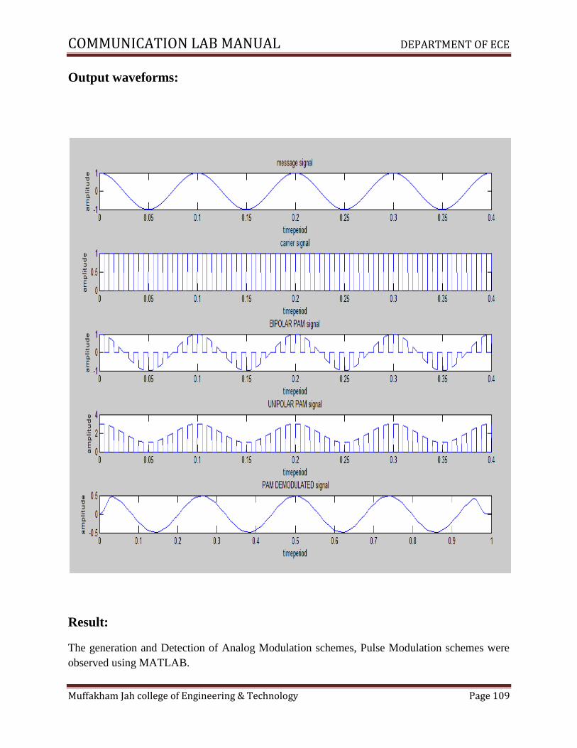
COMMUNICATION LAB MANUAL DEPARTMENT OF ECE
Muffakham Jah college of Engineering & Technology Page 109
Output waveforms:
Result:
The generation and Detection of Analog Modulation schemes, Pulse Modulation schemes were
observed using MATLAB.

COMMUNICATION LAB MANUAL DEPARTMENT OF ECE
Muffakham Jah college of Engineering & Technology Page 110
2.GENERATION & DETECTION OF PCM, DELTA MODULATION & DIGITAL
MODULATION SCHEMES (ASK, FSK, BPSK, QPSK) BY USING MATLAB
Aim:
To Generate & to detect Modulation schemes like PCM, DM and Digital Modulation schemes
like ASK, FSK, BPSK, and QPSK using MATLAB.
Software required: MATLAB2010a
Program:
1. ASK Modulation:
%ASK Modulation
clc;
clear all;
close all;
%GENERATE CARRIER SIGNAL
Tb=1; fc=10;
t=0:Tb/100:1;
c=sqrt(2/Tb)*sin(2*pi*fc*t);
%generate message signal
N=8;
m=rand(1,N);
t1=0;t2=Tb
for i=1:N
t=[t1:.01:t2]
if m(i)>0.5
m(i)=1;
m_s=ones(1,length(t));
else
m(i)=0;

COMMUNICATION LAB MANUAL DEPARTMENT OF ECE
Muffakham Jah college of Engineering & Technology Page 111
m_s=zeros(1,length(t));
end
message(i,:)=m_s;
%product of carrier and message
ask_sig(i,:)=c.*m_s;
t1=t1+(Tb+.01);
t2=t2+(Tb+.01);
%plot the message and ASK signal
subplot(5,1,2);axis([0 N -2 2]);plot(t,message(i,:),'r');
title('message signal');xlabel('t--->');ylabel('m(t)');grid on
hold on
subplot(5,1,4);plot(t,ask_sig(i,:));
title('ASK signal');xlabel('t--->');ylabel('s(t)');grid on
hold on
end
hold off
%Plot the carrier signal and input binary data
subplot(5,1,3);plot(t,c);
title('carrier signal');xlabel('t--->');ylabel('c(t)');grid on
subplot(5,1,1);stem(m);
title('binary data bits');xlabel('n--->');ylabel('b(n)');grid on
% ASK Demodulation
t1=0;t2=Tb
for i=1:N
t=[t1:Tb/100:t2]
%correlator
x=sum(c.*ask_sig(i,:));
%decision device
if x>0
demod(i)=1;
else
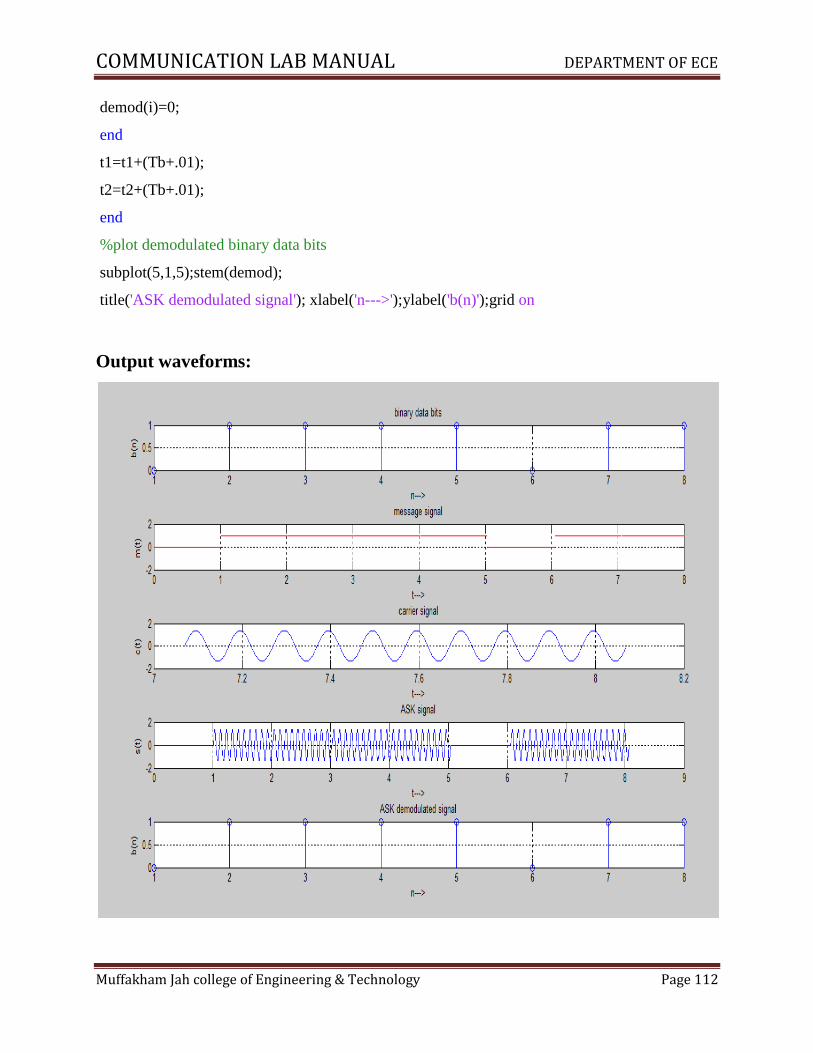
COMMUNICATION LAB MANUAL DEPARTMENT OF ECE
Muffakham Jah college of Engineering & Technology Page 112
demod(i)=0;
end
t1=t1+(Tb+.01);
t2=t2+(Tb+.01);
end
%plot demodulated binary data bits
subplot(5,1,5);stem(demod);
title('ASK demodulated signal'); xlabel('n--->');ylabel('b(n)');grid on
Output waveforms:
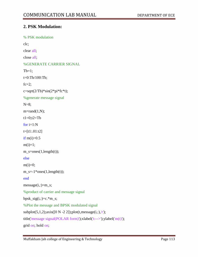
COMMUNICATION LAB MANUAL DEPARTMENT OF ECE
Muffakham Jah college of Engineering & Technology Page 113
2. PSK Modulation:
% PSK modulation
clc;
clear all;
close all;
%GENERATE CARRIER SIGNAL
Tb=1;
t=0:Tb/100:Tb;
fc=2;
c=sqrt(2/Tb)*sin(2*pi*fc*t);
%generate message signal
N=8;
m=rand(1,N);
t1=0;t2=Tb
for i=1:N
t=[t1:.01:t2]
if m(i)>0.5
m(i)=1;
m_s=ones(1,length(t));
else
m(i)=0;
m_s=-1*ones(1,length(t));
end
message(i,:)=m_s;
%product of carrier and message signal
bpsk_sig(i,:)=c.*m_s;
%Plot the message and BPSK modulated signal
subplot(5,1,2);axis([0 N -2 2]);plot(t,message(i,:),'r');
title('message signal(POLAR form)');xlabel('t--->');ylabel('m(t)');
grid on; hold on;
COMMUNICATION LAB MANUAL DEPARTMENT OF ECE
Muffakham Jah college of Engineering & Technology Page 114
subplot(5,1,4);plot(t,bpsk_sig(i,:));
title('BPSK signal');xlabel('t--->');ylabel('s(t)');
grid on; hold on;
t1=t1+1.01; t2=t2+1.01;
end
hold off
%plot the input binary data and carrier signal
subplot(5,1,1);stem(m);
title('binary data bits');xlabel('n--->');ylabel('b(n)');
grid on;
subplot(5,1,3);plot(t,c);
title('carrier signal');xlabel('t--->');ylabel('c(t)');grid on;
% PSK Demodulation
t1=0;t2=Tb
for i=1:N
t=[t1:.01:t2]
%correlator
x=sum(c.*bpsk_sig(i,:));
%decision device
if x>0
demod(i)=1;
else
demod(i)=0;
end
t1=t1+1.01;
t2=t2+1.01;
end
%plot the demodulated data bits
subplot(5,1,5);stem(demod);
title('demodulated data');xlabel('n--->');ylabel('b(n)');
grid on
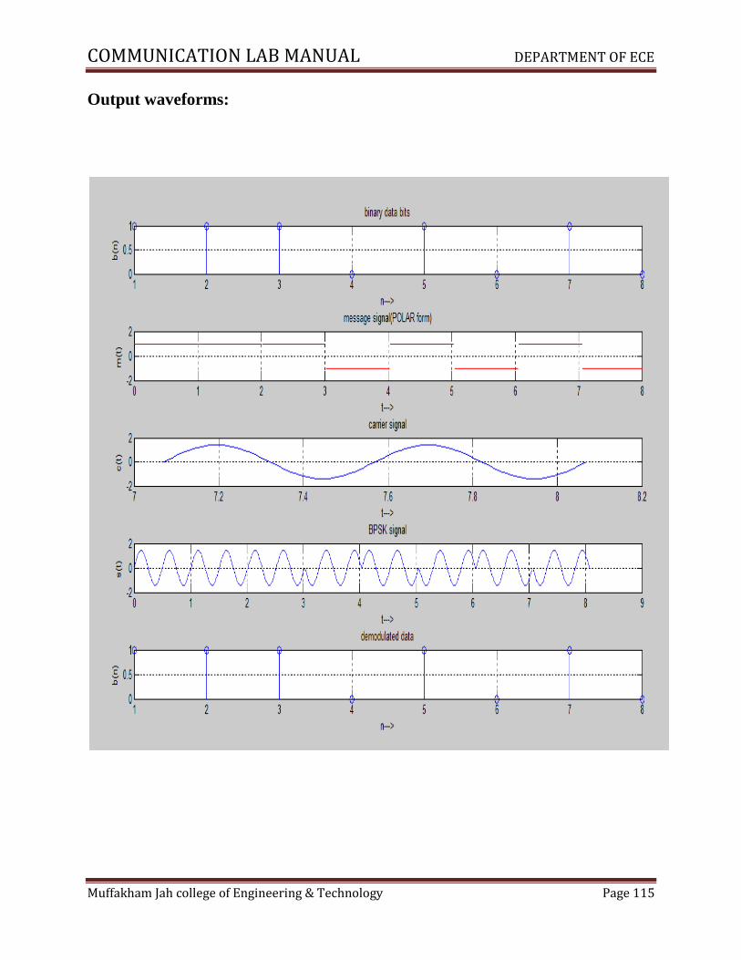
COMMUNICATION LAB MANUAL DEPARTMENT OF ECE
Muffakham Jah college of Engineering & Technology Page 115
Output waveforms:
COMMUNICATION LAB MANUAL DEPARTMENT OF ECE
Muffakham Jah college of Engineering & Technology Page 116
3. FSK Modulation:
% FSK Modulation
clc;
clear all;
close all;
%GENERATE CARRIER SIGNAL
Tb=1; fc1=2;fc2=5;
t=0:(Tb/100):Tb;
c1=sqrt(2/Tb)*sin(2*pi*fc1*t);
c2=sqrt(2/Tb)*sin(2*pi*fc2*t);
%generate message signal
N=10;
m=rand(1,N);
t1=0;t2=Tb
for i=1:N
t=[t1:(Tb/100):t2]
if m(i)>0.5
m(i)=1;
m_s=ones(1,length(t));
invm_s=zeros(1,length(t));
else
m(i)=0;
m_s=zeros(1,length(t));
invm_s=ones(1,length(t));
end
message(i,:)=m_s;
%Multiplier
fsk_sig1(i,:)=c1.*m_s;
fsk_sig2(i,:)=c2.*invm_s;
fsk=fsk_sig1+fsk_sig2;
COMMUNICATION LAB MANUAL DEPARTMENT OF ECE
Muffakham Jah college of Engineering & Technology Page 117
%plotting the message signal and the modulated signal
subplot(3,2,2);axis([0 N -2 2]);plot(t,message(i,:),'r');
title('message signal');xlabel('t---->');ylabel('m(t)');grid on;hold on;
subplot(3,2,5);plot(t,fsk(i,:));
title('FSK signal');xlabel('t---->');ylabel('s(t)');grid on;hold on;
t1=t1+(Tb+.01); t2=t2+(Tb+.01);
end
hold off
%Plotting binary data bits and carrier signal
subplot(3,2,1);stem(m);
title('binary data');xlabel('n---->'); ylabel('b(n)');grid on;
subplot(3,2,3);plot(t,c1);
title('carrier signal-1');xlabel('t---->');ylabel('c1(t)');grid on;
subplot(3,2,4);plot(t,c2);
title('carrier signal-2');xlabel('t---->');ylabel('c2(t)');grid on;
13
% FSK Demodulation
t1=0;t2=Tb
for i=1:N
t=[t1:(Tb/100):t2]
%correlator
x1=sum(c1.*fsk_sig1(i,:));
x2=sum(c2.*fsk_sig2(i,:));
x=x1-x2;
%decision device
if x>0
demod(i)=1;
else
demod(i)=0;
end
t1=t1+(Tb+.01);
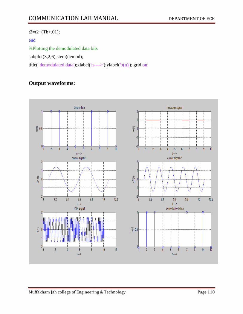
COMMUNICATION LAB MANUAL DEPARTMENT OF ECE
Muffakham Jah college of Engineering & Technology Page 118
t2=t2+(Tb+.01);
end
%Plotting the demodulated data bits
subplot(3,2,6);stem(demod);
title(' demodulated data');xlabel('n---->');ylabel('b(n)'); grid on;
Output waveforms:
COMMUNICATION LAB MANUAL DEPARTMENT OF ECE
Muffakham Jah college of Engineering & Technology Page 119
4. QPSK Modulation:
% QPSK Modulation
clc;
clear all;
close all;
%GENERATE QUADRATURE CARRIER SIGNAL
Tb=1;t=0:(Tb/100):Tb;fc=1;
c1=sqrt(2/Tb)*cos(2*pi*fc*t);
c2=sqrt(2/Tb)*sin(2*pi*fc*t);
%generate message signal
N=16;m=rand(1,N);
t1=0;t2=Tb
for i=1:2:(N-1)
t=[t1:(Tb/100):t2]
if m(i)>0.5
m(i)=1;
m_s=ones(1,length(t));
else
m(i)=0;
m_s=-1*ones(1,length(t));
end
%odd bits modulated signal
odd_sig(i,:)=c1.*m_s;
if m(i+1)>0.5
18
m(i+1)=1;
m_s=ones(1,length(t));
else
m(i+1)=0;
m_s=-1*ones(1,length(t));

COMMUNICATION LAB MANUAL DEPARTMENT OF ECE
Muffakham Jah college of Engineering & Technology Page 120
end
%even bits modulated signal
even_sig(i,:)=c2.*m_s;
%qpsk signal
qpsk=odd_sig+even_sig;
%Plot the QPSK modulated signal
subplot(3,2,4);plot(t,qpsk(i,:));
title('QPSK signal');xlabel('t---->');ylabel('s(t)');grid on; hold on;
t1=t1+(Tb+.01); t2=t2+(Tb+.01);
end
hold off
%Plot the binary data bits and carrier signal
subplot(3,2,1);stem(m);
title('binary data bits');xlabel('n---->');ylabel('b(n)');grid on;
subplot(3,2,2);plot(t,c1);
title('carrier signal-1');xlabel('t---->');ylabel('c1(t)');grid on;
subplot(3,2,3);plot(t,c2);
title('carrier signal-2');xlabel('t---->');ylabel('c2(t)');grid on;
% QPSK Demodulation
t1=0;t2=Tb
for i=1:N-1
t=[t1:(Tb/100):t2]
%correlator
x1=sum(c1.*qpsk(i,:));
x2=sum(c2.*qpsk(i,:));
%decision device
if (x1>0&&x2>0)
demod(i)=1;
demod(i+1)=1;
elseif (x1>0&&x2<0)
demod(i)=1;
COMMUNICATION LAB MANUAL DEPARTMENT OF ECE
Muffakham Jah college of Engineering & Technology Page 121
demod(i+1)=0;
elseif (x1<0&&x2<0)
demod(i)=0;
demod(i+1)=0;
elseif (x1<0&&x2>0)
demod(i)=0;
demod(i+1)=1;
end
t1=t1+(Tb+.01); t2=t2+(Tb+.01);
end
subplot(3,2,5);stem(demod);
title('qpsk demodulated bits');xlabel('n---->');ylabel('b(n)');grid on;

COMMUNICATION LAB MANUAL DEPARTMENT OF ECE
Muffakham Jah college of Engineering & Technology Page 122
Output waveforms:

COMMUNICATION LAB MANUAL DEPARTMENT OF ECE
Muffakham Jah college of Engineering & Technology Page 123
5. Pulse Code Modulation:
clc;
clear all;
t = 0:0.005:20;
partition = -1:0.2:2;
codebook = -1:0.2:2.2;
x = sin(t);
[index,quants] = quantiz(x,partition,codebook);
subplot(3,1,1);
plot(t,x);
title('Message Signal');
xlabel('Time(s) ---->')
ylabel('Amplitude(V) ---->')
subplot(3,1,2);
plot(t,quants);
title('Quantized Signal');
xlabel('Time(s) ---->')
ylabel('Amplitude(V) ---->')
y = uencode(quants,3);
subplot(3,1,3);
plot(t,y);
title('PCM Signal');
xlabel('Time(s) ---->');
ylabel('Amplitude(V) ---->')

COMMUNICATION LAB MANUAL DEPARTMENT OF ECE
Muffakham Jah college of Engineering & Technology Page 124
Output waveforms:
COMMUNICATION LAB MANUAL DEPARTMENT OF ECE
Muffakham Jah college of Engineering & Technology Page 125
5. Delta Modulation:
t=[0:0.01:1] %t is the time we are considering for our calculation. Even signal time period is 1
second
m=sinc(2*pi*t) %genrates the sinc pulse with the time period of t
subplot(211) %opens the figure window and splits it into two parts horizontally
hold on %all the graphs drawn after this command will be plotted on the first part of the figure
plot(m,'*black') %plotting the sinc pulse with the *'s
title('sinc pulse') %putting the title for the graph drawn earlier
xlabel('time')%specifies the xlabel for our graph
ylabel('amplitude')%specifies the ylabel for our figure
d=2*pi/100 %d is the step size we are dividing the total time period into 100 parts of same size
%Logic to calculate the delta modulation signal
%We have total 100 samples over the time period of t
%When the delta modulation we consider error signal is same as the sampled version of the
incoming signal
%and we will quantize the error signal
%mq is the star case approximates signal and is is equal to the previous time frame step
approximation plus the quantized error signal for the current sample
for n=1:1:100
if n==1
e(n)=m(n)
eq(n)=d*sign(e(n))
mq(n)=eq(n)
else
e(n)=m(n)-mq(n-1)
eq(n)=d*sign(e(n))
mq(n)=mq(n-1)+eq(n)
end
end
COMMUNICATION LAB MANUAL DEPARTMENT OF ECE
Muffakham Jah college of Engineering & Technology Page 126
%draw the quantized version of the signal on the graph of original signal
stairs(mq,'red')
hleg=legend('original signal','stair case approximated signal')
hold off
%Deltma Modulation of Sine wave
subplot(212)
hold on
m1=sin(2*pi*t)
plot(m1,'red')
title('sin wave')
xlabel('time')
ylabel('amplitude')
d=2*pi/100
for n=1:1:100
if n==1
e1(n)=m1(n)
eq1(n)=d*sign(e1(n))
mq1(n)=eq1(n)
else
e1(n)=m1(n)-mq1(n-1)
eq1(n)=d*sign(e1(n))
mq1(n)=mq1(n-1)+eq1(n)
end
end
stairs(mq1,'blue')
hleg=legend('original signal','stair case approximated signal')
hold off
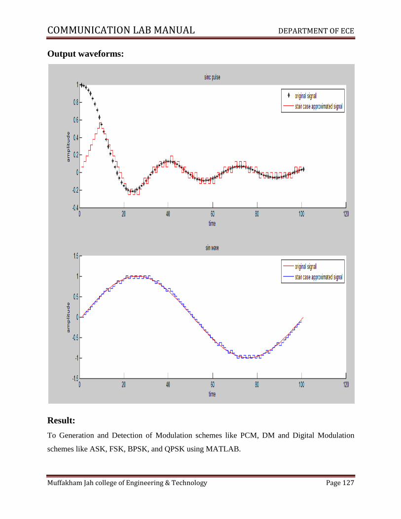
COMMUNICATION LAB MANUAL DEPARTMENT OF ECE
Muffakham Jah college of Engineering & Technology Page 127
Output waveforms:
Result:
To Generation and Detection of Modulation schemes like PCM, DM and Digital Modulation
schemes like ASK, FSK, BPSK, and QPSK using MATLAB.
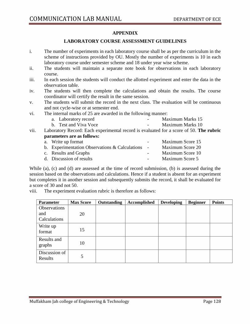
COMMUNICATION LAB MANUAL DEPARTMENT OF ECE
Muffakham Jah college of Engineering & Technology Page 128
APPENDIX
LABORATORY COURSE ASSESSMENT GUIDELINES
i. The number of experiments in each laboratory course shall be as per the curriculum in the
scheme of instructions provided by OU. Mostly the number of experiments is 10 in each
laboratory course under semester scheme and 18 under year wise scheme.
ii. The students will maintain a separate note book for observations in each laboratory
course.
iii. In each session the students will conduct the allotted experiment and enter the data in the
observation table.
iv. The students will then complete the calculations and obtain the results. The course
coordinator will certify the result in the same session.
v. The students will submit the record in the next class. The evaluation will be continuous
and not cycle-wise or at semester end.
vi. The internal marks of 25 are awarded in the following manner:
a. Laboratory record - Maximum Marks 15
b. Test and Viva Voce - Maximum Marks 10
vii. Laboratory Record: Each experimental record is evaluated for a score of 50. The rubric
parameters are as follows: a. Write up format - Maximum Score 15
b. Experimentation Observations & Calculations - Maximum Score 20
c. Results and Graphs - Maximum Score 10
d. Discussion of results - Maximum Score 5
While (a), (c) and (d) are assessed at the time of record submission, (b) is assessed during the
session based on the observations and calculations. Hence if a student is absent for an experiment
but completes it in another session and subsequently submits the record, it shall be evaluated for
a score of 30 and not 50.
viii. The experiment evaluation rubric is therefore as follows:
Parameter Max Score Outstanding Accomplished Developing Beginner Points
Observations
and
Calculations 20
Write up
format 15
Results and
graphs 10
Discussion of
Results 5

COMMUNICATION LAB MANUAL DEPARTMENT OF ECE
Muffakham Jah college of Engineering & Technology Page 129
LABORATORY EXPERIMENT EVALUATION RUBRIC
CATEGORY OUTSTANDING
(Up to 100%)
ACCOMPLISHED
(Up to 75%)
DEVELOPING
(Up to 50%)
BEGINNER
(Up to 25%)
Write up
format
Aim, Apparatus,
material requirement,
theoretical basis,
procedure of
experiment, sketch of
the experimental
setup etc. is
demarcated and
presented in clearly
labeled and neatly
organized sections.
The write up follows
the specified format
but a couple of the
specified parameters
are missing.
The report follows
the specified format
but a few of the
formats are missing
and the experimental
sketch is not
included in the
report
The write up
does not follow
the specified
format and the
presentation is
shabby.
Observations
and
Calculations
The experimental
observations and
calculations are
recorded in neatly
prepared table with
correct units and
significant figures.
One sample
calculation is
explained by
substitution of values
The experimental
observations and
calculations are
recorded in neatly
prepared table with
correct units and
significant figures
but sample
calculation is not
shown
The experimental
observations and
calculations are
recorded neatly but
correct units and
significant figures
are not used. Sample
calculation is also
not shown
The experimental
observations and
results are
recorded
carelessly.
Correct units
significant
figures are not
followed and
sample
calculations not
shown
Results and
Graphs
Results obtained are
correct within
reasonable limits.
Graphs are drawn
neatly with labeling
of the axes. Relevant
calculations are
performed from the
graphs. Equations are
obtained by
regression analysis or
curve fitting if
relevant
Results obtained are
correct within
reasonable limits.
Graphs are drawn
neatly with labeling
of the axes. Relevant
calculations from the
graphs are
incomplete and
equations are not
obtained by
regression analysis or
curve fitting
Results obtained are
correct within
reasonable limits.
Graphs are not
drawn neatly and or
labeling is not
proper. No
calculations are
done from the
graphs and
equations are not
obtained by
regression analysis
or curve fitting
Results obtained
are not correct
within reasonable
limits. Graphs
are not drawn
neatly and or
labeling is not
proper. No
calculations are
done from the
graphs and
equations are not
obtained by
regression
analysis or curve
fitting
Discussion of
results
All relevant points of
the result are
discussed and
justified in light of
theoretical
expectations.
Reasons for divergent
results are identified
and corrective
measures discussed.
Results are discussed
but no theoretical
reference is
mentioned. Divergent
results are identified
but no satisfactory
reasoning is given for
the same.
Discussion of results
is incomplete and
divergent results are
not identified.
Neither relevant
points of the
results are
discussed nor
divergent results
identified
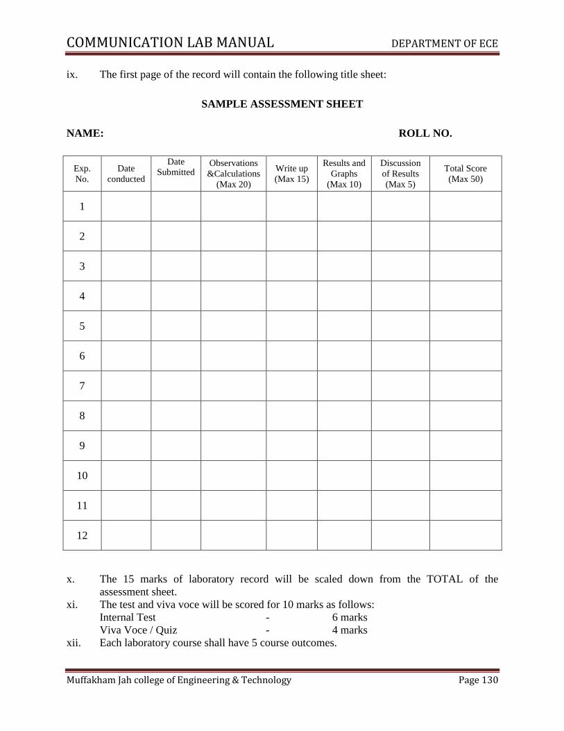
COMMUNICATION LAB MANUAL DEPARTMENT OF ECE
Muffakham Jah college of Engineering & Technology Page 130
ix. The first page of the record will contain the following title sheet:
SAMPLE ASSESSMENT SHEET
NAME: ROLL NO.
Exp.
No.
Date
conducted
Date
Submitted Observations
&Calculations
(Max 20)
Write up
(Max 15)
Results and
Graphs
(Max 10)
Discussion
of Results
(Max 5)
Total Score
(Max 50)
1
2
3
4
5
6
7
8
9
10
11
12
x. The 15 marks of laboratory record will be scaled down from the TOTAL of the
assessment sheet.
xi. The test and viva voce will be scored for 10 marks as follows:
Internal Test - 6 marks
Viva Voce / Quiz - 4 marks
xii. Each laboratory course shall have 5 course outcomes.
COMMUNICATION LAB MANUAL DEPARTMENT OF ECE
Muffakham Jah college of Engineering & Technology Page 131
The proposed course outcomes are as follows:
On successful completion of the course, the student will acquire the ability to:
1. Conduct experiments, take measurements and analyze the data through hands-on
experience in order to demonstrate understanding of the theoretical concepts of
_______________________, while working in small groups.
2. Demonstrate writing skills through clear laboratory reports.
3. Employ graphics packages for drawing of graphs and use computational software for
statistical analysis of data.
4. Compare the experimental results with those introduced in lecture, draw relevant
conclusions and substantiate them satisfactorily.
5. Transfer group experience to individual performance of experiments and demonstrate
effective oral communication skills.
xiii. The Course coordinators would prepare the assessment matrix in accordance with the
guidelines provided above for the five course outcomes. The scores to be entered against
each of the course outcome would be the sum of the following as obtained from the
assessment sheet in the record:
a. Course Outcome 1: Sum of the scores under „Observations and Calculations‟.
b. Course Outcome 2: Sum of the scores under „Write up‟.
c. Course Outcome 3: Sum of the scores under „Results and Graphs‟.
d. Course Outcome 4: Sum of the scores under „Discussion of Results‟.
e. Course Outcome 5: Marks for „Internal Test and Viva voce‟.
xiv. Soft copy of the assessment matrix would be provided to the course coordinators.

COMMUNICATION LAB MANUAL DEPARTMENT OF ECE
Muffakham Jah college of Engineering & Technology Page 132
MUFFAKHAM JAH COLLEGE OF ENGINEERING AND TECHNOLOGY
Program Outcomes of B.E (ECE) Program:
PO1: Engineering knowledge: Apply the knowledge of mathematics, science, engineering fundamentals, and an
engineering specialization to the solution of complex engineering problems.
PO2: Problem analysis: Identify, formulate, research literature, and analyse complex engineering problems reaching
substantiated conclusions using first principles of mathematics, natural sciences, and engineering sciences
PO3: Design/development of solutions: Design solutions for complex engineering problems and design system
components or processes that meet the specified needs with appropriate consideration for the public health and
safety, and the cultural, societal, and environmental considerations.
PO4: Conduct investigations of complex problems: Use research-based knowledge and research methods including
design of experiments, analysis and interpretation of data, and synthesis of the information to provide valid
conclusions.
PO5: Modern tool usage: Create, select, and apply appropriate techniques, resources, and modern engineering and
IT tools including prediction and modeling to complex engineering activities with an understanding of the
limitations.
PO6: The engineer and society: Apply reasoning informed by the contextual knowledge to assess societal, health,
safety, legal, and cultural issues and the consequent responsibilities relevant to the professional engineering practice.
PO7: Environment and sustainability: Understand the impact of the professional engineering solutions in societal
and environmental contexts, and demonstrate the knowledge of, and need for sustainable development.
PO8: Ethics: Apply ethical principles and commit to professional ethics and responsibilities and norms of the
engineering practice.
PO9: Individual and team work: Function effectively as an individual, and as a member or leader in diverse teams,
and in multidisciplinary settings.
PO10: Communication: Communicate effectively on complex engineering activities with the engineering
community and with society at large, such as, being able to comprehend and write effective reports and design
documentation, make effective presentations, and give and receive clear instructions.
PO11: Project management and finance: Demonstrate knowledge and understanding of the engineering and
management principles and apply these to one‟s own work, as a member and leader in a team, to manage projects
and in multidisciplinary environments.
PO 12: Life-long learning: Recognise the need for, and have the preparation and ability to engage in independent
and life-long learning in the broadest context of technological change.
Program Specific Outcomes (PSOs) of ECE Department, MJCET
PSO1: The ECE Graduates will acquire state of art analysis and design skills in the areas of digital and analog VLSI
Design using modern CAD tools.
PSO2: The ECE Graduates will develop preliminary skills and capabilities necessary for embedded system design
and demonstrate understanding of its societal impact.
PSO3: The ECE Graduates will obtain the knowledge of the working principles of modern communication systems
and be able to develop simulation models of components of a communication system.
PSO4: The ECE Graduates will develop soft skills, aptitude and programming skills to be employable in IT sector.
Related Documents