Document Number: Revision: Revision Date: Daniels Electronics Ltd. Victoria, BC PRINTED IN CANADA © 1998–2010 Daniels Electronics Ltd. All rights reserved. No part of this publication may be reproduced, stored in a retrieval system or transmitted in any form or by any means, electronic, mechanical, photocopying, recording or otherwise, without the prior written consent of Daniels Electronics Ltd. The stylized “Daniels Electronics Ltd.” and “DE” logo are registered Canadian and US trademarks of Daniels Electronics Ltd. The stylized “Daniels Electronics Ltd.” and “DE” logo are trademarks of Daniels Electronics Ltd. MT-3 FM TRANSMITTER MAINBOARD INSTRUCTION MANUAL Covers Models: VT-3H035-SXA300 VT-3H045-SXA300 IM20-MT3TXMN 5-0-0 Feb 2010

Welcome message from author
This document is posted to help you gain knowledge. Please leave a comment to let me know what you think about it! Share it to your friends and learn new things together.
Transcript
Document Number:Revision:
Revision Date:
Daniels Electronics Ltd.Victoria, BC
PRINTED IN CANADA
© 1998–2010 Daniels Electronics Ltd. All rights reserved. No part of this publication may be reproduced, stored in a retrieval system or transmitted in any form or by any means, electronic, mechanical, photocopying, recording or otherwise, without the prior written consent of Daniels Electronics Ltd.
The stylized “Daniels Electronics Ltd.” and “DE” logo are registered Canadian and US trademarks of Daniels Electronics Ltd.
The stylized “Daniels Electronics Ltd.” and “DE” logo are trademarks of Daniels Electronics Ltd.
MT-3 FM TransMiTTerMainBoardinsTrucTion Manual
Covers Models:VT-3H035-SXA300VT-3H045-SXA300
IM20-MT3TXMN5-0-0Feb 2010

ii
MT-3 FM Transmitter Mainboard Instruction ManualIM20-MT3TXMN
This document has been produced, verified and controlled in accordance with Daniels Electronics’ Quality Management System requirements.
Please report any errors or problems to Daniels Electronics’ Customer Service Department.
The user’s authority to operate this equipment could be revoked through any changes or modifications not expressly approved by Daniels Electronics Ltd.
The design of this equipment is subject to change due to continuous development. This equipment may incorporate minor changes in detail from the information contained in this manual.
DOCUMENT CONTROL
NOTE
Daniels Electronics Ltd. utilizes a three-level revision system. This system enables Daniels to identify the significance of a revision. Each element of the revision number signifies the scope of change as described in the diagram below.
DOCUMENT REVISION DEFINITION
Major Revisions: The result of a major change to product function, process or
requirements.
Minor Revisions: The result of a minor change to product, process or
requirements.
Editorial Revisions: The result of typing corrections or changes in formatting,
grammar or wording.
1-0-0
Three-level revision numbers start at 1-0-0 for the first release. The appropriate element of the revision number is incremented by 1 for each subsequent revision, causing any digits to the right to be reset to 0.
For example:If the current revision = 2-1-1 Then the next major revision = 3-0-0If the current revision = 4-3-1 Then the next minor revision = 4-4-0If the current revision = 3-2-2 Then the next editorial revision = 3-2-3
The complete revision history is provided at the back of the document.

iii
MT-3 FM Transmitter Mainboard Instruction Manual IM20-MT3TXMN
ContentsGeneral Information ...............................................................1
Introduction ................................................................................................1MT-3 VHF Low Band Performance Specifications .....................................3Physical Specifications ..............................................................................4
Theory of Operation ...............................................................5MT-3 FM Transmitter Mainboard ...............................................................5FM Audio Processor ................................................................................. 12
Transmitter Alignment .......................................................... 23Repair Note .............................................................................................. 23Recommended Test Equipment List ........................................................ 24General Information ................................................................................. 24Synthesizer Module Installation and Removal ......................................... 24Standard Factory Settings and Jumper Configurations ........................... 25MT-3 FM Transmitter Mainboard Interconnection Pin Definitions ............ 26FM Audio Processor Alignment ................................................................ 27Troubleshooting ....................................................................................... 31Temperature Compensation ..................................................................... 32FM Audio Processor Jumper Configurations ........................................... 32
Illustrations and Schematics ................................................ 35MT-3 FM Transmitter Block Diagram ....................................................... 36MT-3 FM Transmitter Mainboard Component Layout – Top..................... 37MT-3 FM Transmitter Mainboard Component Layout – Bottom ............... 38MT-3 FM Transmitter Mainboard Schematic Diagram ............................. 39Front Panel Board Component Layout Diagram ...................................... 40Front Panel Board Schematic Diagram ................................................... 40FM Audio Processor Board Component Layout Diagram ........................ 41FM Audio Processor Board Schematic Diagram ..................................... 42
Parts List .............................................................................. 43MT-3 FM Transmitter Mainboard .............................................................. 43Front Panel Board .................................................................................... 47FM Audio Processor ................................................................................. 47
Revision History ................................................................... 51

iv
MT-3 FM Transmitter Mainboard Instruction ManualIM20-MT3TXMN
This Page Intentionally Left Blank

1
MT-3 FM Transmitter Mainboard Instruction Manual IM20-MT3TXMN
General InformatIon
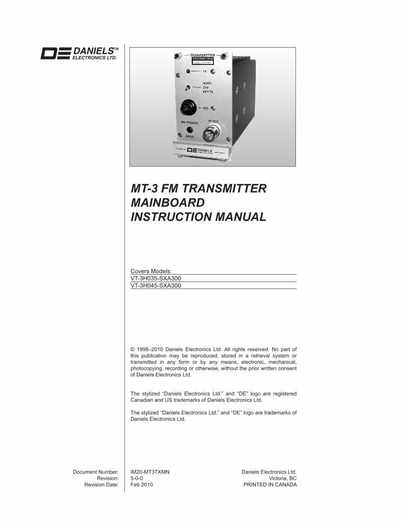
IntroduCtIonThe MT-3 FM Transmitter Mainboard integrates the MT-3 Front Panel Board, MT-3 FM Audio Processor, Synthesizer module and Amplifier module together to comprise a MT-3 series transmitter.
The front panel board and the audio processor are soldered directly to the transmitter mainboard while the amplifier and the synthesizer modules are frequency band sensitive, plug-in modules.
Circuitry and jumpers on the transmitter mainboard control the operation of the modules as well as the overall operation of the MT-3 FM transmitter. Power and signal connections are made through the 48-pin Type F connector on the rear of the transmitter mainboard where they are then routed to the other MT-3 modules.
The transmitter enclosure is formed by the front panel face plate and aluminum shell attached to the transmitter mainboard and the rear panel plate attached to the aluminum shell.

2
MT-3 FM Transmitter Mainboard Instruction ManualIM20-MT3TXMN
This Page Intentionally Left Blank

General Information 3
MT-3 FM Transmitter Mainboard Instruction Manual IM20-MT3TXMN
mt-3 VHf low Band PerformanCe SPeCIfICatIonS
Parameter SpecificationFrequency Range: 29 to 38 MHz (VT-3H035-SWA300)
38 to 50 MHz (VT-3H045-SWA300)Carrier Frequency Stability: ± 5.0 ppm (-30°C to +60°C, Optional -40°C to +60°C)Channel Spacing: 20 kHzChannel Selection: 5.0 or 6.25 kHz incrementsNumber of Channels: 16
Compatibility: MT-3 Series Radio SystemsRF Output Power: 0.5 to 3.0 WEmission Designator: 16K0F3EImpedance (Input): 50 Ω; Type-N connectorDuty Cycle: 100 % (-40°C to +60°C)Undesired Emissions (Conducted Harmonics):Undesired Emissions (Conducted Spurious):
<= -90 dBc<= -80 dBc
VSWR Protection: < 20:1 VSWR at all phase anglesOperating Temperature Range: -30°C to +60°COperating Humidity: 95% RH (non-condensing) at +25°COperating Voltage: +13.8 VDC nominal input (range +10 to +17 VDC)
+9.5 VDC regulatedTransmit Current: <1.2 A for 3.0 W outputStand By Current: 15 mA (Mode 1)
160 mA (Mode 2)185 mA (Mode 4)
PTT Time-Out-Timer: Nominal – 5 minutesRange – 1 sec to 8 hours, disable
Audio Input: 600 Ω balanced or unbalanced input (5 K Ohm)-25 dBm to 0 dBm
Audio Frequency Response: Pre-emphasis: complies with TIA-603CFlat: +1 dB/-3 dB 100 Hz to 3 kHz
Audio Deviation Limiting: ± 5.0 kHzAudio Distortion: <2.0% @ +23°C
<2.5% -40°C to +60°CFM Hum and Noise Ratio: <= -55 dB (0.3 to 3.4 kHz, de-emphasis off)IC Certification No.: 142A-VT3X0X5S (RSS-119)FCC ID: H4JVT-3H040-S (FCC Parts 22, 90)
General Information4
MT-3 FM Transmitter Mainboard Instruction ManualIM20-MT3TXMN
PHySICal SPeCIfICatIonS
Physical Dimensions: Width: 7.1 cm (2.8 in) Height: 12.8 cm (5.05 in) Depth: 19 cm (7.5 in)Module Weight: 1.4 kg (3.0 lbs)Corrosion Prevention: Anodized aluminum construction•
Stainless steel hardware• Gold-plated module connectors•
Module Design: Compact Eurostandard modular design• Plug-in modules mate with the Daniels standard MT-3 Repeater Subrack• Subracks / modules comply with IEEE 1101, DIN 41494 and IEC 297-3 • (mechanical size / modular arrangement)
External Connections: RF Connection – Type-N connector located on the module front panel.Motherboard connections (Audio, Power, and Control) are made through a 48-pin, gold-plated, Type-F connector on the rear of the module.
User connection is made through mated motherboard assembly of the radio subrack. Type-F connector complies with DIN 41612 Level 2 (200 mating cycles, 4-day 10 ppm SO2 gas test with no functional impairment and no change in contact resistance).
Handle Text Colour: Orange

5
MT-3 FM Transmitter Mainboard Instruction Manual IM20-MT3TXMN
tHeory of oPeratIon
mt-3 fm tranSmItter maInBoard GeneralSwitch SW1 on the Front Panel Board is a double pole, double throw (DPDT) switch that controls the operation of the transmitter.
When SW1 is in the OFF position the transmitter is turned off; however, +13.8 VDC is still present on the transmitter mainboard as the +13.8 VDC supply is not switched. When SW1 is in the KEYED position, +9.5 VDC is supplied to the transmitter circuitry and the transmitter is continuously keyed on. When SW1 is in the NORM position, +9.5 VDC is supplied to the transmitter circuitry and the transmitter can be keyed from any of the several Push-To-Talk inputs.

Theory of Operation6
MT-3 FM Transmitter Mainboard Instruction ManualIM20-MT3TXMN
transmitter Push-to-talkAll three of the Push-To-Talk (PTT) inputs that key the transmitter are active low (< +2 VDC). One PTT input is on the front panel microphone connector. The other two PTT inputs: PTT WTO (PTT with Time-Out-Timer) and PTT NTO (PTT No Time-Out-Timer) are on the backplane connector of the transmitter board. If required, the microphone’s PTT input can be configured to activate the transmitter’s Time-Out-Timer (TOT). An isolated PTT input can be made available by installing an optional relay (RELAY1) and configuring jumpers J1 to J4 so that the relay controls the PTT circuitry.
microphone PttJumper J1 on the Front Panel Board configures the microphone’s PTT input (MIC PTT) to either bypass or activate the transmitter’s TOT. Installing surface mount jumper J1 in the ‘X’ position (default) selects the MIC PTT NTO line, which bypasses the TOT. Installing surface mount jumper J1 to the ‘Y’ position selects the MIC PTT WTO line, which activates the transmitter’s TOT. When SW1 is in the KEYED position, the MIC PTT NTO line is automatically grounded.
Ptt with time-out-timerPins B10 and Z10 of the backplane connector are the PTT WTO input. When the PTT WTO signal, which is normally high, falls below +2.0 VDC, the transmitter is keyed. The transmitter is disabled when the PTT WTO input rises above +2.3 VDC or if the TOT’s time-out period is exceeded. If the time-out period is exceeded, the PTT WTO input must go high (> +2.3 VDC) and then low again in order to re-key the transmitter.
The PTT WTO threshold of approximately +2 VDC (0.3 VDC hysteresis) is set by U1a, R1, R2, R3, R4, R9 and R10 while diodes D1 and D2 provide over-voltage protection for U1a. The PTT WTO signal output from U1a is ‘AND’ed with the MIC PTT WTO by U2a. When either the PTT WTO or the MIC PTT WTO is activated, the output of U2a goes low, which triggers the transmitter’s TOT located on the FM Audio Processor. The TOT’s output is ‘AND’ed with the MIC PTT NTO signal (U2c) and the PTT NTO signal (U2d).
When any one of the preceding three signals (TOT’s output, MIC PTT NTO, PTT NTO) go low, the transmitter is activated by transistors Q1 to Q7 which switch power to the various modules.
Ptt no time-out-timerPins B14 and Z14 of the backplane connector are the PTT NTO input. When the PTT NTO signal, which is normally high, falls below +2.0 VDC, the transmitter is keyed. As long as the PTT NTO signal remains below +2.0 VDC, the transmitter will remain keyed. The transmitter is disabled when the PTT NTO signal rises above +2.3 VDC.
The PTT NTO threshold of approximately +2 VDC (0.3 VDC hysteresis) is set by U1b, R5, R6, R7, R8, R9 and R10 while diodes D3 and D4 provide over-voltage protection for U1b. The PTT NTO signal is ‘AND’ed with the output of U2c (MIC PTT NTO signal ‘AND’ed with the TOT output) by U2d. When the output of U2d goes low, transistors Q1 to Q7 activate the transmitter, which switch power to the various modules.
Ptt relayThe transmitter’s PTT circuitry can be completely isolated by installing RELAY1. Jumpers J1 to J5 configure the relay to provide an isolated PTT input for either the PTT WTO line or PTT NTO line. Energizing the relay enables the isolated PTT input. The transmitter board will accept any of the Aromat TF2E line relays. These relays are DPDT, single side stable, and have coil voltages ranging from +3 VDC to +48 VDC. Only one set of relay contacts is used to activate the PTT circuitry.
To configure the isolated input for PTT WTO operation, jumpers J2, J3 and J4 must be in the ‘Y’ position. In this mode, pins B10 and Z10 no longer function as the PTT WTO input; however, pins B14 and Z14 continue to function as the normal PTT NTO input.
To configure the isolated input for PTT NTO operation, jumpers J2, J3 and J4 must be in the ‘X’ position. In this mode, pins B14 and Z14 no longer function as the PTT NTO input; however, pins B10 and Z10 continue to function as the normal PTT WTO input.

Theory of Operation 7
MT-3 FM Transmitter Mainboard Instruction Manual IM20-MT3TXMN
Ptt outputPin B24 on the backplane connector is an open drain output (Q9), which is pulled low anytime the transmitter is keyed and the synthesizer is locked. An N-channel MOSFET Q9 is capable of sinking currents up to two amps and is activated by Q8, which is activated by the Qualified PTT signal (JS2-6) of the synthesizer module. The Qualified PTT signal also controls the LED ENA line for diode D1 on the front panel board and enable line for the MT-3 Amplifier Module (JP1-1).
Ptt Voltage SwitchingThe PTT voltage switching circuitry is comprised of transistors Q1 through Q7 and the associated resistors. The base of Q1 is driven by the output of U2d, which is the combined PTT signal from all of the PTT inputs. When the transmitter is keyed, Q1 is turned off and subsequently transistors Q3, Q4 and Q6 are turned on.
Transistors Q3, Q4 and Q6 provide three separate functions:
Q3 Provides the active low signal for the synthesizer module PTT input.
Q4 Turns on Q5, which turns on the +9.5 VDC Switched supply.
Q6 Turns on Q7, which turns on the +9.5 VDC PTT Switched supply.
The +9.5 VDC Switched supply (Q5) can also be activated by installing jumper J6 or by externally grounding the TX Standby Line (pins B12 and Z12). The +9.5 VDC PTT Switched supply and the +9.5 VDC Switched supply both provide +9.5 VDC but, depending on how jumpers J6, J7 and J18 are configured, the transmitter’s standby mode will change.
front Panel BoardThe Front Panel Board is attached to the MT-3 FM Transmitter Mainboard and is used to mount the front panel switch, diode and microphone connector. The main purpose of the board is to eliminate a wiring harness for the front panel components. Jumper J1, located on the rear of the circuit board, is used to select whether or not the MIC PTT line activates the transmitter’s TOT. Jumper J2 is used to select whether or not RX Audio or 13.8 Volt is supplied to Pin 4 of the microphone.
J1 X position MIC PTT NTO – no time-out-timer (factory setting)
Y position MIC PTT WTO with time-out-timer
J2 X position RX Audio enabled to MIC-4 pin (factory setting)
Y position +13.8 Volts supplied to MIC-4 pin

Theory of Operation8
MT-3 FM Transmitter Mainboard Instruction ManualIM20-MT3TXMN
transmitter Standby modesThe MT-3 series transmitters have eight different standby modes that trade off standby current consumption for start-up speed. Three jumpers are found on the transmitter mainboard:
J6 Continuously enables the +9.5 VDC switched supply.
J7 Selects the power source for the FM Audio Processor.
J18 Selects the enable line for the Synthesizer module.
Additionally, there is a jumper on the FM Audio Processor Board:
JU36 Determines the power source for the dual compression amplifiers.
If JU36 is not installed on the FM Audio Processor, both microphone and balanced audio compression amplifiers will be disabled, eliminating the use of the front panel microphone jack for local microphone operations. With this configuration, the balanced audio is routed around the compression circuitry via JU11 (installed) with JU1 and JU2 removed.
mode Condition table
mode # J6 J7 J18Synthesizer/ osc. State
audio Processor State (8 V Switched)
audio Processor Compression Ju36
1a out y y Ptt Switched Ptt Switched Switched +8.0 V (X)1b out y y Ptt Switched Ptt Switched Continuous 9.5 V (y)1c out y y Ptt Switched Ptt Switched disabled (not Installed)2a In y X always enabled Ptt Switched Switched +8.0 V (X)2b In y X always enabled Ptt Switched Continuous 9.5 V (y)2c In y X always enabled Ptt Switched disabled (not Installed)3 In X y Ptt Switched always enabled doesn’t matter4 In X X always enabled always enabled doesn’t matter

Theory of Operation 9
MT-3 FM Transmitter Mainboard Instruction Manual IM20-MT3TXMN
The actual current and start-up time depend on the oscillator source and amplifier module. The current and start-up times given below are representative values intended only as guidelines. For further information, refer to the appropriate modular instruction manuals for specific oscillator and amplifier types.
Standby mode Selection tablemode # Standby Current turn-on time
1a 14 ma 150 mS1b 21 ma 10 mS1c 14 ma 10 mS2a 166 ma 150 mS2b 173 ma 10 mS2c 167 ma 10 mS3 29 ma 10 mS4 181 ma 10 mS
NOTE: Standby Current is the total current drawn by the synthesizer and FM Audio Processor from the +9.5 VDC supply.
fm audio Processor total Current Consumption
Compression Configuration
audio Processor Current draw Keyed / unkeyed
Compression enabled (Ju36 X) 15 ma / 0.45 maCompression and microphone disabled (Ju36 open)
9.2 ma / 0.45 ma
Compression enabled (Ju36 y) 15 ma / 9.2 ma
audio CircuitsThe FM Audio Processor performs audio signal conditioning (e.g., limiting, filtering and pre-emphasis). The transmitter mainboard routes the audio lines from the backplane connector to the audio processor and then to the synthesizer.
The audio lines routed to the audio processor are two subtone inputs (backplane pins B22 and Z24), a direct modulation input (pin Z28), a squelched / flat audio input (pin Z20), a 600 Ω balanced input (pins B18 and Z18), and an audio control line (pin Z22). The audio processor’s balanced input pins are isolated from pins B18 and Z18 by a transformer (T1).
Two audio outputs from the FM Audio Processor are routed to the synthesizer modules.
microphone audioNormally the microphone audio is sent from the attached transmitter, however the MIC IN and MIC OUT lines can be configured on the transmitter mainboard such that the microphone audio modulates a different transmitter. The configuration of the MIC IN (pin Z4) and MIC OUT (pin B4) lines on the MT-3 FM Transmitter Mainboard are controlled by jumpers J16 and J17 respectively. Jumper J16 selects the audio source for the FM Audio Processor’s microphone input. Jumper J17 is used to enable or disable the MIC OUT line. Normally the transmitter’s microphone is selected (J16 in the X position) and the MIC OUT line is enabled (J17 is installed).
received audioPin B20 is the audio input from the transmitter’s corresponding receiver. The default setting for this line is to have it AC coupled (Jumper J9 is out) and directly connected to the front panel board RX AUDIO line.
Channel SelectionSynthesized transmitter Seven backplane connections are used to communicate with the synthesizer unit. Pins D28, D30 and D32 are used (in house) to program the synthesizer. Channel select lines CSEL 0 (least significant bit) through CSEL 3 (most significant bit), which are available at pins D20, D22, D24 and D26, are used once the synthesizer is programmed to select one of 16 channels. If the channel select lines are all low (Channel 1) the channel for the synthesizer is read from switches FSW1 (most significant), FSW2, FSW3 and FSW4 (least significant); otherwise one of 15 pre-programmed frequencies is selected. Refer to the channel designation tables (manual IM20-VT3H040CT) to set the operating frequency.

Theory of Operation10
MT-3 FM Transmitter Mainboard Instruction ManualIM20-MT3TXMN
Amplifier CircuitsThe MT-3 series Amplifier has six connections that are cabled to the transmitter board:
+13.8 VDC• +9.5 VDC• Enable• Forward Power Sense• Reverse Power Sense• Ground•
The +13.8 VDC supply (JP1-3) is always on while the +9.5 VDC supply (JP1-2) is always switched by a PTT signal. The enable line (JP1-1) is active low and is controlled by the Qualified PTT signal from the synthesizer module.
Jumpers J12, J13, J14 and J15 are used to configure the amplifier’s forward and reverse power sense lines (JP1-4 and JP1-5). Normally jumpers J13, J14 and J15 are in the X position, which directly connects the amplifier’s forward and reverse power sense lines to the backplane connector (pins B26 and Z26 respectively).
The forward and reverse power sense lines from the amplifier can be open collector or linear outputs depending on how they are configured in the amplifier module. In open collector configuration, the lines are active low, that is, the output will go low when a “fail” condition is detected. If both lines from the amplifier module are configured as open collector outputs, the power sense lines can be ‘OR’ed together to make a general fail indicator (jumper J12 in, jumpers J13, J14 and J15 in the Y position).
The Fail Indicator is also an open collector output; however, the Fail Indicator is active high (the output goes high when a “fail” condition is detected). When the transmitter is configured with the general fail indicator option, pin Z26 (VSWR reverse) is not used and pin B26 becomes the Fail Indicator output.

Theory of Operation 11
MT-3 FM Transmitter Mainboard Instruction Manual IM20-MT3TXMN
time-out-timer CircuitryThe MT-3 FM Transmitter also has an associated programmable push-to-talk (PTT) time-out-timer (TOT) circuitry on the transmitter mainboard. The TOT circuitry is powered via J34 from the continuous +9.5 VDC supply and is programmable for various time-out periods.
The TOT input trigger (enabled by J33) is normally high and in this state the timer is disabled. When the input trigger level falls below +2.0 VDC, the timer is activated, the TOT output trigger (enabled by J35) is pulled low and the transmitter is keyed. If the input trigger rises above +2.4 VDC or if the time-out period is exceeded, the output trigger will go high, disabling the transmitter. If the time-out period is exceeded, the TOT input trigger must go high and then low again in order to re-key the transmitter.
The time-out duration is jumper selectable from 1 second to 8 hours (see Table 1). The positions of the jumpers are on the top (through-hole component) side of the transmitter mainboard.
J32 J31 J29 J28 J26 J27 Minutes I I I I I I 0.01 I I I I I n/I 0.01 I I I I n/I I 0.01 I I I n/I I I 0.01 I I I n/I I n/I 0.02 I I n/I I I I 0.02 I I I n/I n/I I 0.03 I I n/I I I n/I 0.04 I I n/I n/I I I 0.05 I I n/I I n/I I 0.06 I I n/I n/I I n/I 0.08 I n/I I I I I 0.10 I I n/I n/I n/I I 0.12 I n/I I I I n/I 0.15 I n/I I n/I I I 0.19 I n/I I I n/I I 0.23 I n/I I n/I I n/I 0.31 I n/I n/I I I I 0.38 I n/I I n/I n/I I 0.47 I n/I n/I I I n/I 0.62 I n/I n/I n/I I I 0.75 I n/I n/I I n/I I 0.94 I n/I n/I n/I I n/I 1.25 n/I I I I I I 1.5 I n/I n/I n/I n/I I 1.88 n/I I I I I n/I 2.5 n/I I I n/I I I 3.0 n/I I I I n/I I 3.75 N/I I I N/I I N/I 5.0 n/I I n/I I I I 6.0 n/I I I n/I n/I I 7.5 n/I I n/I I I n/I 10 n/I I n/I n/I I I 12 n/I I n/I I n/I I 15 n/I I n/I n/I I n/I 20 n/I n/I I I I I 24 n/I I n/I n/I n/I I 30 n/I n/I I I I n/I 40 n/I n/I I n/I I I 48 n/I n/I I I n/I I 60 n/I n/I I n/I I n/I 80 n/I n/I n/I I I I 96 n/I n/I I n/I n/I I 120 n/I n/I n/I I I n/I 160 n/I n/I n/I n/I I I 192 n/I n/I n/I I n/I I 240 n/I n/I n/I n/I I n/I 320 n/I n/I n/I n/I n/I I 480
N/I = Not InstalledI = InstalledBold text represents default settings.
TABLE 1: Time-out Jumper Settings and Duration

Theory of Operation12
MT-3 FM Transmitter Mainboard Instruction ManualIM20-MT3TXMN
fm audIo ProCeSSor
IntroductionThe FM Audio Processor is a versatile circuit board that can provide several types of audio processing for voice or data transmission (see Figure 1).
Bandwidth table
term Channel Spacingrated System deviation
wide band (wB) 25 kHz or 30 kHz ±5.00 kHz
Features include:
• Automatic level control using a compression amplifier with a 25 dB dynamic range
• Limiter and splatter filter that removes noise and harmonics
• Selectable pre-emphasis or flat audio response
• Temperature compensated audio output
• Ability to transmit data and voice switched by a single control line
• Multiple jumpers that can be configured to allow maximum flexibility in routing signals from inputs to outputs and disabling selected circuits to reduce operating current
• Dual microphone and balanced audio compression circuits
• On-board multi-configurable temperature compensation to correct for changes in transmitter deviation over temperature caused by changing characteristics of synthesizers and oscillators
• A single chip 10th Order Linear Phase Low Pass Splatter Filter for increased cut-off attenuation responses
• Separate voice and direct modulation outputs, each individually configurable
• Direct modulation input for LTR®, DCS, paging and other digital modulations that require very low frequency modulation to the synthesizer module
• Multiple audio inputs for various audio filter or modulation configurations
NOTE: If dual mode CTCSS and LTR® / DCS is desired in the same transmitter, it may be possible with dual port modulation synthesizers. It is not feasible with single port modulation synthesizers. These synthesizers are characterized by the lack of a modulation port in their VCO circuit. Contact the Daniels factory for further details.
A continuous +9.5 VDC supply and a switched +8.0 VDC supply are required to power the module which is normally supplied by the transmitter mainboard.
The FM Audio Processor’s balanced input pins are isolated by a transformer (T1) on the transmitter mainboard. Two audio outputs from the FM Audio Processor are routed to the synthesizer module.

Theory of Operation 13
MT-3 FM Transmitter Mainboard Instruction Manual IM20-MT3TXMN
fm audio Processor Block diagram
SplatterFilter
Pre-emphasis
Select
Pre-emphasis
Select
CompressionAmp
CompressionAmp
Limiter/SummingAmplifier
Buffer
+4 VRegulator
+4 V
Pre-emphasis
Select
AuxillaryBufferAmp
Tx AudioControl
AudioSwitch 1
AudioSwitch 2
Regular ModulationBuffer
Subtone1
3 KHz
Direct ModulationOffset Buffer
TCVCXOModulation Buffer
Offset
TCVCXODC Level
Adjust
Reg ModOut
Low FreqOut
Inverting Amp
CouplingSelect
2 PortPolaritySelect
JU35
JU34
Tx AudioControl
3dBNarrowBandPad
JU14
JU26
JU27
JU30
JU43
JU28
JU25
49K9
49K9
P1-3
R2
U1A
U1B
P1-1
R31
ToneDigitalInput
P2-1
BalancedInput
MicrophoneInput
U3A
U3B
U2A
U2C
U2D
P2-2
R48
R42
U5
U6
Q1
DirectModulationInput
P4-3U2B
R87
P4-4
P4-2
P3-1
U3C
U3D
P4-1JU4
Subtone2 JU13
R36
JU12
JU11
B0232
*
FIGURE 1

Theory of Operation14
MT-3 FM Transmitter Mainboard Instruction ManualIM20-MT3TXMN
Factory ConfigurationThe FM Audio Processor is factory configured as follows:
Parameter Specification
Maximum Deviation ±5.0 kHz
Microphone Input • 1 kHz signal at -10 dBm gives ±60% rated system deviation • 1 kHz signal compression set at ±84% rated system deviation
Audio Balanced Input • 1 kHz tone at -8 dBm gives pre-emphasis response ±60% rated system deviation • 1 kHz signal compression set at ±84% rated system deviation
Subtone Input 1 100 Hz tone at -18 dBm gives ±500 Hz
All Other Audio Inputs Disabled
Interconnection Pin Layout Diagram
PCB
1
2
3
4
1
2
3
4
1
2
3
4
1
2
3
4
P1P2P4P3
Balanced Input
END VIEW
Mic Input
Subtone Inp ut 1
+8V
+9.5V
Low Frequency Direct Mod Output
VoiceAnd Subtone
Output -8 dBm
-10 dBm
-18 dBm
Surface Mount Side
0 dBm
B0312
FIGURE 2
For the interconnections and functions of the FM Audio Processor external connections, see Figure 2. Connectors P1, P2, P3, and P4 are four-pin audio processor headers soldered directly to the transmitter mainboard. For troubleshooting isolation, the audio processor could be unsoldered from the mainboard and analyzed. Power and I/O connections, as well as their expected levels, are shown in this diagram.

Theory of Operation 15
MT-3 FM Transmitter Mainboard Instruction Manual IM20-MT3TXMN
turn-on timeTurn-on Time is the time it takes the FM Audio Processor to output a stable audio signal to P3-1 once the +8.0 VDC power is enabled. The turn-on time can be virtually eliminated by configuring the audio processor for continuous audio standby; however, this results in increased current consumption. Powering of the compression amplifier contributes to most of the time delay, so transmitters configured with the compression amplifier disabled (for data or non-compressed audio) will exhibit the fast turn-on time. The response measurement is made with the standard factory settings with a 1 kHz tone applied to the balanced input.
low frequency modulationThe transmitter has an additional option to address low frequency user modulation requirements. A phase modulated bandwidth from 0 (DC) to 100 Hz (PLL loop filter bandwidth) allows specialized applications such as paging or trunking where a separate low frequency digital / analog modulation channel is required. Low Frequency Modulation allows external access to the low frequency modulation capabilities of the synthesizer module. The DIRECT MODULATION inputs on the J1 control connector of the MT-3 Motherboard will be used (B20 for TX A, and A20 for TX B).
turn on timemode turn-on time audio Processor Standby Currentfast turn on – higher current approx 1 mS 15 maCurrent save – slower response approx 150 mS 450 µa
fm audio Processor SignalsThe FM Audio Processor has six audio inputs, two audio outputs and one audio control input. Five of the audio inputs are used primarily for voice and tone signals. The sixth, the Direct Modulation Input, is used primarily for data signals. The audio control input is used to switch audio outputs so the transmitter can transmit voice or data.
The audio inputs on the audio processor are:
• Dynamic microphone input
• 600 Ω balanced input
• Subtone inputs
• Auxiliary input
• Direct modulation input for data signals
fm audio Processor outputsBoth the audio outputs, Modulation Output (P3-1) and Low Frequency / Direct Modulation Output (P4-2), are gated by audio switches U5 and U6 respectively which are controlled by the Transmit Audio Control Input (P4-4). The audio switches can be operated complimentary to each other so that only one source modulates the transmitter. In standard configuration, the Modulation Output port is used so switch U5 is always on.

Theory of Operation16
MT-3 FM Transmitter Mainboard Instruction ManualIM20-MT3TXMN
fm audio Processor modulation outputsThe Modulation Output port is used by all voice input signals. The voice inputs are passed to U1A and U1B, a dual programmable compressor-expander that is configured as an automatic level control amplifier. Op-Amp U3A provides the limiting action for the audio processor.
After the audio signals have been combined, limited and buffered, they are filtered by a 10th order Linear Phase Low Pass Filter (U4). The output signal from the filter is then level adjusted by the deviation control pot, R29, at the input of buffer amplifier U3D. In special applications, jumper JU6 can be disabled and JU7 enabled allowing the transmitter to be modulated directly from the auxiliary input. External filtering may be required since jumper JU7 bypasses the limiting and filter circuits.
The Low Frequency / Direct Modulation Output port has two functions depending on whether the transmitter is synthesized. In a synthesized transmitter, this port is used to modulate the synthesizer reference frequency. The frequency response of this port is typically DC to 300 Hz.
fm audio Processor microphone Input The microphone input has an automatically level controlled (ALC) pre-amplifier U1 whose input level is controlled by R2. The microphone input level control (R2) can accommodate a -25 dBm to 0 dBm input signal. The microphone input is limited and filtered and is output at the standard modulation output port. The microphone input can have a standard 6 dB/octave pre-emphasis response or a flat-audio response, jumper JU1 at Y and X position respectively.
fm audio Processor Balanced InputThe 600 Ω balanced input uses the ALC pre-amplifier U1B with input level control pot (R31). The balanced input level control can accommodate a -25 dBm to 0 dBm input. (Install JU17 when using the lower input levels). Like the microphone input, the balanced input is limited and filtered and is output at the standard modulation output port.
If no compression is required (i.e., customer is providing their own), JU11 can be enabled providing a path through R48 (Auxiliary Input Level Control) to amplifier U2C where pre-emphasis or flat audio can then be selected from its output.
fm audio Processor auxiliary InputThe auxiliary input is a special input and does not have an ALC. This input can be configured for a pre-emphasis response (enable JU9 Y) or a flat-audio response (enable JU9 X). The level for this input is set by R48. The auxiliary output is normally summed with the voice signals by Op-Amp U3A, limited, then filtered and output at the standard modulation output port. The value of R57 (Select) can be tailored for specific applications.
When jumper JU6 is disabled and jumper JU7 is enabled, the auxiliary input can be used to directly modulate the transmitter. Care should be taken when directly modulating the transmitter with the auxiliary input because the MT-3 transmitters use direct FM modulation and there is no filtering or limiting action provided by the auxiliary input. The input level to the auxiliary input should be -18 dBm and can be driven by one of three inputs:
• balanced input – JU11
• tone / digital input – JU12 X or Y enabled
• direct modulation input – through JU28
When the 600 Ω balanced input is connected to the auxiliary input, the balanced input level control can be used to adjust the level for the auxiliary input.

Theory of Operation 17
MT-3 FM Transmitter Mainboard Instruction Manual IM20-MT3TXMN
fm audio Processor Subtone InputsThere are two subtone inputs available on the FM Audio Processor. Both subtone inputs can be individually configured to be output from the standard Modulation Output port or to be output from the Low Frequency / Direct Modulation Output. In standard configuration, Subtone 1 is summed with the voice signals to be output from the standard Modulation Output port while Subtone 2 is used for DCS. Both subtone inputs have an input level control.
In order to maintain a uniform frequency response from 50 Hz to 300 Hz, dual-port modulation techniques are used. Refer to the schematic diagrams and alignment procedures included in this manual.
direct modulation InputThe Direct Modulation Input is an extremely versatile input. This port is designed to be used for data signals. Depending on the application, the signal can be amplified, AC or DC coupled and output to the Modulation Output or the Low Frequency / Direct Modulation Output port. Please consult the factory for specific jumper settings for your application.
Theory of Operation18
MT-3 FM Transmitter Mainboard Instruction ManualIM20-MT3TXMN
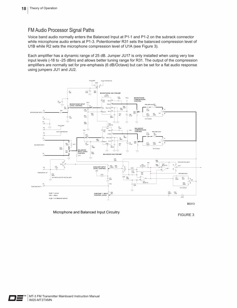
fm audio Processor Signal PathsVoice band audio normally enters the Balanced Input at P1-1 and P1-2 on the subrack connector while microphone audio enters at P1-3. Potentiometer R31 sets the balanced compression level of U1B while R2 sets the microphone compression level of U1A (see Figure 3).
Each amplifier has a dynamic range of 25 dB. Jumper JU17 is only installed when using very low input levels (-18 to -25 dBm) and allows better tuning range for R31. The output of the compression amplifiers are normally set for pre-emphasis (6 dB/Octave) but can be set for a flat audio response using jumpers JU1 and JU2.
BALANCEDINPUT LEVELCONTROL
FLAT AUDIO
PRE-EMPHASISMICROPHONE INPUTLEVEL CONTROL
BALANCED INPUT
hi gh = voi cel ow = dat a
X
Y
+9.5V CONTINUOUS
NOT INSTALLED FOR DIGITAL MOD.
AUXILIARY INPUT LEVEL CONTROL
X Y
MICROPHONE AGC PREAMP
BALANCED AGC PREAMP
hi gh = w i deband sel ect
X
Y
BALANCEDCOMPRESSIONCONTROL
FLAT AUDIO
PRE-EMPHASIS
MICROPHONECOMPRESSIONCONTROL
X
Y
X
Y
X
Y
FLAT AUDIO
PRE-EMPHASIS
X
Y
TWO PORT POLARITY
SUBTONE 1 INPUTCONTROL LEVEL
3P1
2P1
1P1
4P1
3P3
3P2
1P2
4
P2+9.5V CONTINUOUS
C1010nF
4K53R46
C510nF
1
23
R25K0
FB1
+8.0V SWD
+8.0V SWD
1
2
3
JU5
47uFC13
3
2
1
100K0R48
680nFC7
4.7uFC8
TP3
SELR57
N/I (22nF)C32
Rect In
Var G
Rect Cap
Output
Inv In
R3
THD Trim
15
14
16
10
12
11
9
U1SA571D
a
680nFC42
TP12
4.7uFC26
Vcc
Rect In
Var G
Rect Cap
Output
Inv In
R3
THD Trim
GND
2
3
1
7
5
6
8
13
4
SA571DU1b
2P2
JU16
9
108
U2MC33174
c
R74N/I
R73N/I
13
1214
U2MC33174
d
4.0V
TP6
R4311K8
C39680nF
3
2
1
5K0R42
C351.0uF
C11.0uF
C91.0uF
C301.0uF
R8210K0
C373.3nF
R4916k2
C1410nF
4.0V
R7616k2
C161.0uF
JU33C511.0uF
1
2
3
JU12
R3915K4R41
137K
R5920K0
R6215K4
R51M00
C251.0uF
R6018K2R61
18K2
R82K21
R949K9
R418K2R6
18K2
330nFC36
C153.3nF
R72K21
R1049K9330nF
C19
C21.0uF
R5110K0
2
1
3
JU1
2
1
3
JU2
JU11
TP11
TP4
JU10
R52100K
R65100K
C383.3nF
R112K21
R4049K9
2
1
3JU14
1
23
R315K0
R30604R
TP2
0R0R1
R64100K
R560R0
C41.0uF
231
JU36
JU17
1
2
3JU9
1
23
5K0R63
3
21
5K0R38
MICROPHONE INPUT
SUBTONE INPUT 1
TONE/DIGITAL I/P
Microphone and Balanced Input Circuitry
B0313
FIGURE 3

Theory of Operation 19
MT-3 FM Transmitter Mainboard Instruction Manual IM20-MT3TXMN
XY
X
Y
X
Y
10 POLE LOWPASS FI LTER
LIMITER TEMPERATURECOMPENSATION
2 13
JU22
R16100K
C1710nF C49
10nF
+8.0V SWD
JU6
C504.7uF
JU7
SELR23
N/IR24
SELR25
N/IR26
SELR28
SELR17
SELR18
SELR20
In+
In-
Gnd
V-
Vout
V+
Rx
Div/Clk
1
2
3
4
8
7
6
5
U4LTC1569-6
R6622K1
R6730K9
R683K48
R692K00
+8.0V SWDP11
P12
P9 P10
2
34
1
11
U3MC33174
a
6
57
U3MC33174
b
1 2
R19SEL
1 2SELR27
12
C211.0uF
12
C61.0uF
4.0V4.0V
+8.0V SWD
TP5
R8410K0
R8510K0
TP10
1 2
150pFC43 TP14
1
2
3
JU24
1
2
3
JU3
Limiter and Splatter Filter
B0314
The microphone and balanced audio signals are summed and limited by U3A. Op-Amp U3B provides audio level temperature compensation (for synthesizer sensitivity variations). Due to the many different characteristics of various synthesizers, many components are selected for best performance over the temperature range.
The audio is then filtered by a 10th order linear phase low pass splatter filter U3a and U3B (see Figure 4). This is to provide the linearity and cut-off attenuation response required for narrow band operation and digital applications.
The filter output level is set by R29, the deviation control. From this point, the signal goes to U5 a bilateral audio switch. U5 is normally configured to be always on. The output of U5 goes to the final buffer amplifier U3D. Installing JU23 lowers the audio level by one half facilitating a quick conversion of a wide band transmitter for narrow band operation. The output of U3D has many capacitors with values selected depending on the installed synthesizer module type.
FIGURE 4

Theory of Operation20
MT-3 FM Transmitter Mainboard Instruction ManualIM20-MT3TXMN
If no compression circuitry is required, the balanced input signals can be routed around the compression circuitry using jumper JU11. Op-Amp U2C then provides buffering and amplification. Pre-emphasis filtering at the output is enabled or disabled using jumper JU9. The audio signal is then normally routed to U3A, the summing amplifier / limiter and processed as indicated previously.
NOTE: If compression is bypassed (see Figure 5), the THD may be higher due to the reduced dynamic input range causing more clipping. “Key down” current consumption can be reduced by 9 mA by disconnecting the compression amplifier power (removing JU36), however, the microphone circuit will be disabled.
Assuming no data modulation, a second way to route around audio compression is via the direct modulation port P4-3 and route through JU28 to R48 and Op-Amp U2C. Sub-audible tones enter at P2-2 where level is controlled by R42. A single jumper JU16 enables the audio path to U3A, the summing amplifier / limiter.
BALANCEDINPUT LEVELCONTROL
FLAT AUDIO
PRE-EMPHASISMICROPHONE INPUTLEVEL CONTROL
BALANCED INPUT
hi gh = voi cel ow = dat a
X
Y
+9.5V CONTINUOUS
NOT INSTALLED FOR DIGITAL MOD.
AUXILIARY INPUT LEVEL CONTROL
X Y
MICROPHONE AGC PREAMP
BALANCED AGC PREAMP
hi gh = w i deband sel ectl ow = nar r ow band sel ect
X
Y
BALANCEDCOMPRESSIONCONTROL
FLAT AUDIO
PRE-EMPHASIS
MICROPHONECOMPRESSIONCONTROL
X
Y
X
Y
X
Y
FLAT AUDIO
PRE-EMPHASIS
X
Y
TWO PORT POLARITY
SUBTONE 1 INPUTCONTROL LEVEL
3P1
2P1
1P1
4P1
3P3
3P2
1P2
P4
4
P2+9.5V CONTINUOUS
C1010nF
4K53R46
C510nF
1
23
R25K0
FB1
+8.0V SWD
+8.0V SWD
1
2
3
JU5
47uFC13
3
2
1
100K0R48
680nFC7
4.7uFC8
TP3
SELR57
N/I (22nF)C32
Rect In
Var G
Rect Cap
Output
Inv In
R3
THD Trim
15
14
16
10
12
11
9
U1SA571D
a
680nFC42
TP12
4.7uFC26
Vcc
Rect In
Var G
Rect Cap
Output
Inv In
R3
THD Trim
GND
2
3
1
7
5
6
8
13
4
SA571DU1b
2P2
JU16
9
108
U2MC33174
c
R74N/I
R73N/I
13
1214
U2MC33174
d
4.0V
TP6
R4311K8
C39680nF
3
2
1
5K0R42
C351.0uF
C11.0uF
C91.0uF
C301.0uF
R8210K0
C373.3nF
R4916k2
C1410nF
4.0V
R7616k2
C161.0uF
JU33C511.0uF
1
2
3
JU12
R3915K4R41
137K
R5920K0
R6215K4
R51M00
C251.0uF
R6018K2R61
18K2
R82K21
R949K9
R418K2R6
18K2
330nFC36
C153.3nF
R72K21
R1049K9330nF
C19
C21.0uF
R5110K0
2
1
3
JU1
2
1
3
JU2
JU11
TP11
TP4
JU10
R52100K
R65100K
C383.3nF
R112K21
R4049K9
2
1
3JU14
1
23
R315K0
R30604R
TP2
0R0R1
R64100K
R560R0
C41.0uF
231
JU36
JU17
1
2
3JU9
1
23
5K0R63
3
21
5K0R38
MICROPHONE INPUT
SUBTONE INPUT 1
TONE/DIGITAL I/P
Bypassing Compression
B0315
FIGURE 5

Theory of Operation 21
MT-3 FM Transmitter Mainboard Instruction Manual IM20-MT3TXMN
Voltage regulator U2A provides a regulated +4.0 VDC to all Op-Amp stages. Optional potentiometer R14 can be installed (and JU15 removed) for special applications where a voltage other than +4.0 VDC is required.
Data normally enters at P4-3, the Direct Modulation Input, and is connected via many possible routes selected with jumpers. JU43 allows direct or on-board capacitor coupling. Op-Amp U2B can be configured as a buffer with a DC offset to accommodate input data that has a positive DC voltage offset. The data signals can be sent to gain buffers U2C and U2D through potentiometer R48. Jumper JU14 is normally installed so that the output from U2D provides the correct data polarity when using two-port modulation. See Figure 6.
A single TX Audio control line on P4-4 has 2 functions. It can be configured to switch U3D inputs between data and voice. Alternately, it can be configured to remotely switch between wide band and narrow band applications by switching between the regular audio path and one carrying half the audio level as determined by resistive divider comprised of R22 and R21.
X Y
DEVIATIONCONTROL
LOW FREQUENCY / DIRECT MODULATION OUTPUT
X Y
XY
X
Y
10 POLE LOWPASS FI LTER
X
Y
X
Y
VOICE + SUBAUDIBLE
DCS, LTR
X
Y
TCXO DCLEVELADJUST
TCXO MODULATIONLEVEL ADJUST
WIRE JUMPERFOR DUAL PORTMODULATIONONLY
- - - - - - ->
1P3
2
P4JU37
2 13
JU22
+9.5V CONTINUOUS
4.7uFC45
4.7uFC28
1
2
3
R2950K0
R5549K9
R7510K0
E
B
C
Q1BC817-25
+8.0V SWD
JU6
JU31
R440R0
R45N/I
C121.0nF
R54SEL
12
3
R3650K0
JU32
SELR32
JU29
47uFC34
R12N/I
R7949K9
In+
In-
Gnd
V-
Vout
V+
Rx
Div/Clk
1
2
3
4
8
7
6
5
U4LTC1569-6
R6622K1
R6730K9
R683K48
R692K00
+8.0V SWDP11
P12
P9 P10
9
108
U3MC33174
c
0R0R72
0R0R58
12
C211.0uF
12
C61.0uF
R3749K9
R3449K9
4.0V
C2410nF
+8.0V SWD
4.0V
JU23
TP7
TP8
TP9
SELR81
JU41
10nFC41
R8610K0
3
2
1
R8350K0
R53N/I
R8027K4
+8.0V SWD
1
2
3
JU35
R7810K0
2
3
1
JU39
12
3JU34
JU38
C23330pF
C44330pF
13
1214
U3MC33174
d
R35SEL
JU8
100nFC27
1.0uFC33
1.0uFC40
1.0uFC471.0uFC46
1
2
3 JU25
R2249K9
R2149K9
1 2
3
4
5
U5TC4S66F
1 2
3
4
5
U6TC4S66F
4.0V
R5049K9
R8849K9
JU26 4.0VC55100nF
JU44
33nFC56
+9.5V CONTINUOUS
R7720K0
JU18
21 3
JU19
2
3
1
JU21
1 2JU45
R89100R
Tx Audio Control
TX Audio Control Circuitry
Tx Audio Control
B0316
FIGURE 6

22
MT-3 FM Transmitter Mainboard Instruction ManualIM20-MT3TXMN
This Page Intentionally Left Blank

23
MT-3 FM Transmitter Mainboard Instruction Manual IM20-MT3TXMN
tranSmItter alIGnment
rePaIr noteMT-3 FM Transmitter modules are mainly made up of surface mount devices which should not be removed or replaced using an ordinary soldering iron. Removal and replacement of surface mount components should be performed only with specifically designed surface mount rework and repair stations complete with Electrostatic Discharge (ESD) Protection.
When removing Surface Mount Solder Jumpers, it is recommended to use solder braid in place of manual vacuum type desoldering tools. This will help prevent damage to the circuit boards.

Transmitter Alignment24
MT-3 FM Transmitter Mainboard Instruction ManualIM20-MT3TXMN
reCommended teSt equIPment l IStAlignment of the complete transmitter requires the following test equipment or its equivalent. It is assumed that any adjustment of the transmitter mainboard will also involve the other modules.
Dual Power Supply: Regulated +9.5 VDC at 2 A (e.g., Topward TPS-4000) Regulated +13.8 VDC at 2 A
Oscilloscope: 20 MHz or better (e.g., Fluke 97 Scopemeter)
Digital Multimeter: For DC, RMS AC voltage and current (e.g., Fluke 75)
Radio Communications Test Set: E.g., Marconi Instruments 2955R
VSWR 3:1 Mismatch Load: E.g., JFW 50T-035-3.0:1
Alignment Tool: Johanson 4192
Audio Signal Generator: 600 Ω output impedance, 67 Hz to 5 kHz range
It is recommended that the radio communications test set be frequency-locked to an external reference (WWVH, GPS, Loran C) so that the high stability oscillator may be accurately set to within its ±1 ppm frequency tolerance.
General InformatIonBefore proceeding with the transmitter alignment, check that the appropriate jumpers are installed. See Standard Factory Settings and Jumper Configuration section.
Transmitter alignment is simplified by using a MT-3 Subrack, SM-3 System Regulator and RF extender cable to provide transmitter power and signal interconnection. Alternatively, connect power and audio to the subrack connector as follows:
Subrack Connector P1 Pin+9.5 VdC B6, Z6+13.8 VdC B2, Z2Ground B30, Z30, B32, Z32600 Ω Balanced Audio across B18 and Z18
SyntHeSIZer module InStallatIon and remoValTo remove the Synthesizer module, simply remove the centre screw from the module lid and pull the module out. The module should be pulled straight out so that the four alignment pins do not bend or damage the circuit board.
Installation of the synthesizer module is facilitated by alignment pins on each corner of the module. When the four pins are aligned with their corresponding hole in the transmitter mainboard, push the module down, ensuring that the connector pins on the bottom of the synthesizer module are not bent.

Transmitter Alignment 25
MT-3 FM Transmitter Mainboard Instruction Manual IM20-MT3TXMN
Standard faCtory SettInGS and JumPer ConfIGuratIonSThe standard jumper configuration for the transmitter mainboard is normally employed for transmitter alignment. In a standard configuration, the only alignment required on the MT-3 FM Transmitter Mainboard for a synthesized transmitter is to set the frequency switches (FSW1, FSW2, FSW3 and FSW4) for the desired channel frequency. FSW1 is the most significant digit of the frequency switches. The switch settings for the desired channel frequency can be found in the channel designation tables (IM20-VT3H040CT).
mt-3 fm transmitter mainboard JumpersJumper DefaultPosition Description
J2 X Optional relay configurationJ3 X Optional relay configurationJ4 y Optional relay configurationJ6 not Installed transmitter standby mode select – mode 1J7 y audio processor standby mode selectJ9 not Installed receiver audio aC/dC input couplingJ12 not Installed Amplifier power sense output configurationJ13 X Amplifier power sense output configurationJ14 X Amplifier power sense output configurationJ15 X Amplifier power sense output configurationJ16 X Microphone configurationJ17 Installed microphone output line J18 y Synthesizer module standby mode selectJ19 X 600 Ω audio transformer enable; Y position disablesJ20 X 600 Ω audio transformer enable; Y position disablesJ21 not Installed +8 VdC audio processor supply bypassJ22 X 600 Ω audio transformer enable; Y position disablesJ23 X 600 Ω audio transformer enable; Y position disablesJ24 Installed Subtone #2 output enableJ25 X audio output enableJ26 Installed time-out-timer timing resistor selectJ27 not Installed time-out-timer timing resistor selectJ28 not Installed time-out-timer timing period output selectJ29 Installed time-out-timer timing period output selectJ31 Installed time-out-timer timing period output selectJ32 not Installed time-out-timer timing period output selectJ33 Installed time-out-timer input enableJ34 Installed time-out-timer power enableJ35 Installed time-out-timer output enable
NOTE: Jumpers J1, J5, J8, J10 and J11 designations are not used.

Transmitter Alignment26
MT-3 FM Transmitter Mainboard Instruction ManualIM20-MT3TXMN
MT-3 FM Transmitter Mainboard Standard Factory Configuration
The MT-3 FM Transmitter Mainboard is factory-configured as follows:
• Transmitter Standby Mode 1 (lowest standby current consumption)
• Receiver squelched; de-emphasized audio amplifier disabled
• Optional relay installed, but with active ground contact disabled
• Separate amplifier power sense outputs
mt-3 fm tranSmItter maInBoard InterConneCtIon PIn defInIt IonSThe MT-3 series transmitter employs a 48-pin Eurostandard connector for interfacing to all transmitter power, audio and control functions. Following are the MT-3 series transmitter backplane connections to the MT-3 Motherboard:
Pin Name Pin Name Pin Named2 no Connect B2 +13.8 VdC Z2 +13.8 VdCd4 no Connect B4 mIC out Z4 mIC Ind6 no Connect B6 +9.5 VdC Z6 +9.5 VdCd8 no Connect B8 relay Positive Z8 relay negatived10 no Connect B10 Ptt wto Z10 Ptt wtod12 no Connect B12 tX Standby Z12 tX Standbyd14 no Connect (ImC1) B14 Ptt nto Z14 Ptt ntod16 no Connect (ImC2) B16 no Connect (mt-2 +9.5 V) Z16 no Connect (mt-2 +9.5 V)d18 no Connect (ImC3) B18 Balanced Input 2 Z18 Balanced Input 1d20 Channel Select 0 (lSB) B20 Squelched, de-emph audio In Z20 Squelched, flat audio Ind22 Channel Select 1 B22 Subtone Input 1 Z22 tX audio Controld24 Channel Select 2 B24 Ptt output Z24 Subtone Input 2d26 Channel Select 3 (mSB) B26 forward Power Sense Z26 VSwr reverse Sensed28 Synth tX data (output) B28 rX monitor out Z28 direct mod Inputd30 Synth rx data (Input) B30 Ground Z30 Groundd32 Synth Bootstrap (Input) B32 Ground Z32 Ground

Transmitter Alignment 27
MT-3 FM Transmitter Mainboard Instruction Manual IM20-MT3TXMN
fm audIo ProCeSSor alIGnmentPrior to commencing the standard deviation adjustment procedure, determine the specific configuration of the transmitter (e.g., flat audio, pre-emphasis).
The following points should be noted:
• If the transmitter’s operating frequency is changed beyond the factory recommended bandwidth or if the synthesizer is changed, the FM Audio Processor should be realigned to optimize the transmitter’s performance. The settings tolerance is +/- 0.1 kHz.
• There are slight differences when setting up the transmitter for Flat Audio or Pre-emphasized audio. Although the tuning procedure is the same, there will be skipped sections depending on the transmitter type being tested.
• Although the transmitter is most commonly set up for a single frequency operation, there are times when an application requires multiple frequencies per transmitter. This also changes the standard tuning procedure slightly.
• Due to the variations in the circuitry between models of synthesizer, oscillator and audio processor, version specific tuning steps are outlined in italics.
• Section C is not an alignment procedure but is included as a final performance measurement that confirms correct audio processor alignment.
multiple Channel transmittersIn the tuning of the FM Audio Processor for multiple channel transmitters, the procedures on the following pages apply.
NOTE: The maximum deviation is set on the channel, which gives the maximum deviation when using a 1.8 kHz tone @ +10 dBm. Once that level is set (R29), it is not adjusted again.
The rest of the tuning instructions are carried out while the transmitter frequency is set for the channel, which is roughly in the middle of the band of pre-programmed channels.

Transmitter Alignment28
MT-3 FM Transmitter Mainboard Instruction ManualIM20-MT3TXMN
transmitters with Pre-emphasis and CtCSS Subtone
Section a: Balanced and Subtone audio Setup
Step Reference Action DesiredResults Notes1. R2 (Mic I/P)
R29 (Deviation)R31 (Balanced)R38 (Compress)R42 (Subtone1)R63 (Mic Comp)R36 (TCXO)
Turn Fully CW.Turn Fully CW.Turn Fully CW.Turn Fully CW.Turn Fully CW.Turn Fully CW.Turn Fully CCW.
AF Filter: Low Pass5 kHz or 15 kHz
2. Balanced Input P1-1 and P1-2
Set AF tone freq, level and filter.
AF Gen: 1.8kHz@+10dBm
3. R29 (Deviation) Adjust R29 for deviation. Donotre-adjust.
± 4.4 kHz
4. Subtone 1 input Apply tone. AF Gen: 1kHzTone@-18dBm
5. R42 (Subtone1) Adjust and measure. ± 500 Hz Deviation Monitor
6.
OST-3H035-(2-Port)OST-3H045-(2-Port)
Change AF Gen. freq. AF Gen: 40 Hz @ -18dBm
7. R36 (TCXO) Adjust and measure. ± 500 Hz
8. Subtone 1 input Change AF Gen. freq. AF Gen: 300 Hz @ -18dBm
9. Deviation Monitor Should measure. 500 Hz Tolerance on this measurement is ± 50Hz
10. Deviation Monitor Sweep AF Gen. freq. between 67 Hz and 250 Hz. Measure resultant deviation.
± 300 Hz to 700 Hz
11. Balanced Input P1-1 and P1-2
Change frequency and level.
AF Gen: 1 kHz Tone @ +10dBm
12. R38 (Compress) Adjust and measure. Distortion Analyzer AF Filter: 15 kHz4.0% THD
13. AF Gen. Change level 1 kHz Tone @ -8dBm
14. R31 (Balanced) Adjust and measure. ± 3 kHz Deviation Monitor
15. AF Gen Change level. 1kHzTone@ -18dBm
16. R31 (Balanced) Measure and confirm. ± 1 kHz Tolerance on this measurement is ± 50 Hz

Transmitter Alignment 29
MT-3 FM Transmitter Mainboard Instruction Manual IM20-MT3TXMN
Section B: microphone audio Setup
Step Reference Action DesiredResults Notes
17. Microphone Input Front Panel Pin 2 Apply Tone. AF Gen: 1kHzTone
@+10dBm
A
DATE: 28 MARCH 2005
TITLE: TX MICROPHONE CONNECTOR DETAILS
DRAWN BY: EVA DANIELS
REV DATE: - - -DWG No: B0486-01
DANIELSELECTRONICS LTD
TM1
11
21
2
12
22
3
13
23
4
14
24
5
15
25
6
16
26
7
17
27
8
18
28
9
19
29
10
20
30
FRONT VIEW
3 2
4 1
MIC AUDIO
MIC GND
MIC Connector – Front View
18. R63(MicComp) Adjust and measure. Distortion Analyzer AF Filter: 15 kHz 4.0% THD
19. Microphone Input Front Panel Pin 2
Change level. AF Gen: 1kHzTone@-10dBm
20. R2 (Microphone) Adjust and measure. ± 3 kHz Deviation monitor
21. Microphone Input Front Panel Pin 2
Change level. AF Gen: 1kHzTone@-20dBm
22. R2 (Microphone) Measure and confirm ± 50 Hz.
± 1 kHz Deviation monitor
Section C: audio frequency response and deviation
Step Reference Action DesiredResults Notes
23. AF Gen level Set and measure. AF Gen: +10dBm
24. Balanced Audio Input Sweep from 300 Hz to 2.5 kHz in 100 Hz steps.
± 5.0 kHz Deviation should not exceed maximum deviation.
25. Balanced Audio Input Apply tone. AF Gen 1 kHz @-18dBm
26. Perform AF Frequency Response from 300 Hz to 5 kHz.
As per test sheet limits (FIT-018)

Transmitter Alignment30
MT-3 FM Transmitter Mainboard Instruction ManualIM20-MT3TXMN
transmitters with flat audio
Section a: Balanced and Subtone audio Setup
Step Reference Action DesiredResults Notes1. R2 (Mic I/P)
R29 (Deviation)R31 (Balanced)R38 (Compress)R42 (Subtone1)R63 (Mic Comp)R36 (TCXO)
Turn Fully CW.Turn Fully CW.Turn Fully CW.Turn Fully CW.Turn Fully CW.Turn Fully CW.Turn Fully CCW.
AF Filter: Low Pass5 kHz or 15 kHz
NO COMPRESSION
NO COMPRESSION
2. Balanced Input P1-1 and P1-2
Set AF Gen. freq, level and filter.
AF Gen: 1.8 kHz @ +10dBm
3. R29 (Deviation) Adjust R29 for deviation. Donotre-adjust.
± 4.4 kHz
4. Subtone 1 input Apply tone. AF Gen: 1kHzTone@-18dBm
5. R42 (Subtone1) Adjust and measure. ± 500 Hz Deviation Monitor
6. OST-3H035-(2-Port)OST-3H045-(2-Port)
Change AF Gen. freq. AF Gen: 40 Hz @ -18dB
7. R36 (TCXO) Adjust and measure. ± 500 Hz
8. Subtone 1 input Change AF Gen. freq. AF Gen: 300 Hz @ -18dBm
9. Deviation Monitor Should measure. 500 Hz Tolerance on this measurement is ± 50 Hz
10. Deviation Monitor Sweep AF Gen. freq. between 67 Hz and 250 Hz. Measure resultant deviation.
± 300 Hz to 700 Hz
11. AF Gen Change level. 1 kHz Tone @ -8dBm
12. R31 (Balanced) Adjust and measure. ± 3 kHz Deviation Monitor
Section B: microphone audio Setup
Step Reference Action DesiredResults Notes
13. Microphone Input Front Panel Pin 2
Change level. AF Gen: 1kHzTone@-10dBm
A
DATE: 28 MARCH 2005
TITLE: TX MICROPHONE CONNECTOR DETAILS
DRAWN BY: EVA DANIELS
REV DATE: - - -DWG No: B0486-01
DANIELSELECTRONICS LTD
TM1
11
21
2
12
22
3
13
23
4
14
24
5
15
25
6
16
26
7
17
27
8
18
28
9
19
29
10
20
30
FRONT VIEW
3 2
4 1
MIC AUDIO
MIC GND
MIC Connector - Front View
14. R2 Adjust and measure. ± 3kHz Deviation Monitor
Transmitter Alignment 31
MT-3 FM Transmitter Mainboard Instruction Manual IM20-MT3TXMN
trouBleSHootInG
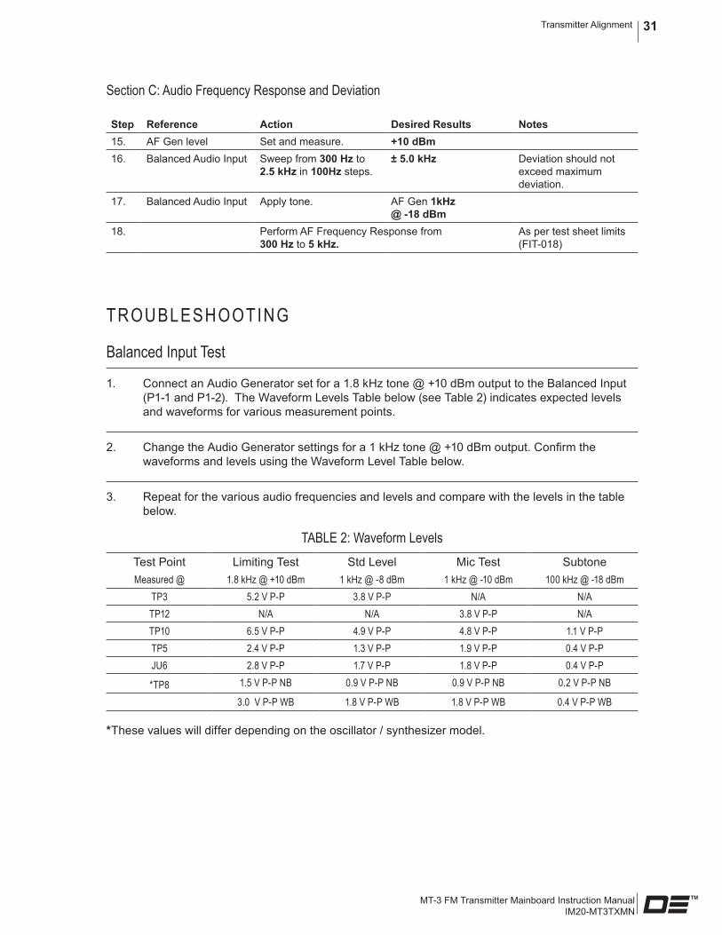
Balanced Input test
1. Connect an Audio Generator set for a 1.8 kHz tone @ +10 dBm output to the Balanced Input (P1-1 and P1-2). The Waveform Levels Table below (see Table 2) indicates expected levels and waveforms for various measurement points.
2. Change the Audio Generator settings for a 1 kHz tone @ +10 dBm output. Confirm the waveforms and levels using the Waveform Level Table below.
3. Repeat for the various audio frequencies and levels and compare with the levels in the table below.
TABLE 2: Waveform LevelsTest Point Limiting Test Std Level Mic Test Subtonemeasured @ 1.8 kHz @ +10 dBm 1 kHz @ -8 dBm 1 kHz @ -10 dBm 100 kHz @ -18 dBm
tP3 5.2 V P-P 3.8 V P-P n/a n/atP12 n/a n/a 3.8 V P-P n/atP10 6.5 V P-P 4.9 V P-P 4.8 V P-P 1.1 V P-PtP5 2.4 V P-P 1.3 V P-P 1.9 V P-P 0.4 V P-PJu6 2.8 V P-P 1.7 V P-P 1.8 V P-P 0.4 V P-P
*tP8 1.5 V P-P nB 0.9 V P-P nB 0.9 V P-P nB 0.2 V P-P nB
3.0 V P-P wB 1.8 V P-P wB 1.8 V P-P wB 0.4 V P-P wB
*These values will differ depending on the oscillator / synthesizer model.
Section C: audio frequency response and deviation
Step Reference Action DesiredResults Notes15. AF Gen level Set and measure. +10dBm16. Balanced Audio Input Sweep from 300 Hz to
2.5 kHz in 100Hz steps.± 5.0 kHz Deviation should not
exceed maximum deviation.
17. Balanced Audio Input Apply tone. AF Gen 1kHz @-18dBm
18. Perform AF Frequency Response from 300 Hz to 5 kHz.
As per test sheet limits(FIT-018)

Transmitter Alignment32
MT-3 FM Transmitter Mainboard Instruction ManualIM20-MT3TXMN
frequency response testMeasurements are made at JU8 with respect to ground.
1. Reduce Audio Generator level to –18 dBm (98 mV RMS).
2. Step frequency to 300, 500, 1000, 2000 and 2500 Hz.
3. Ensure that the results conform to the 6 dB/octave +/- 1 dB from 500 Hz to 2500 Hz referenced to 1000 Hz (+1/-2 dB at 300 Hz).
Subtone Input test
1. Change Audio Generator frequency to 100 Hz and maintain level at –18 dBm (98 mV RMS).
2. Connect signal to Subtone Input 1 (P2-2) and ground (P1-4).
3. Refer to the Waveform Levels Table above and confirm levels.
temPerature ComPenSatIonThe FM Audio Processor includes temperature compensation circuitry to maintain a constant transmitter audio deviation with a fixed level input signal. It is capable of not only compensating for temperature related level variations within the audio processor (typically –0.3 to –0.5 dB at –40ºC), but can also compensate for changes caused by the synthesizer that is not equipped with its own temperature compensation.
Specifications:When a 1.8 kHz tone is applied at a level of +10 dBm to the balanced input of the transmitter, the transmitter deviation shall be ±4.4 kHz at room temperature and can vary from ±4.4 kHz to ±5.0 kHz from -40ºC to +60ºC.
Since the specifications of the components used in the synthesizer or oscillator may change over time, changes to the temperature compensation circuit may be necessary even for the same type of equipment.
Contact the factory for more information on values used.
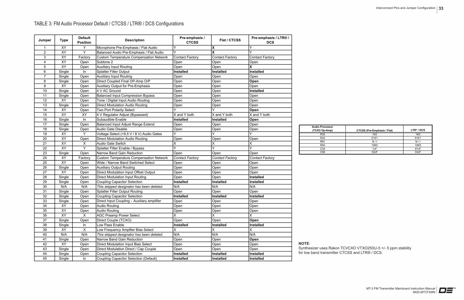
fm audIo ProCeSSor JumPer ConfIGuratIonSFor Default / CTCSS / LTR® / DCS configurations, see Table 3.
MT-3 FM Transmitter Mainboard Instruction Manual IM20-MT3TXMN
Interconnect Pins and Jumper Configuration 33
TABLE 3: FM Audio Processor Default / CTCSS / LTR® / DCS Configurations
NOTE:Synthesizer uses Rakon TCVCXO VTXO250U-5 +/- 5 ppm stability for low band transmitter CTCSS and LTR® / DCS.
AudioProcessor(V2.3)LowBandTXJumperTable
Jumper Type DefaultPosition Description Pre-emphasis/
CTCSS Flat/CTCSS Pre-emphasis/LTR®/DCS
1 XY Y Microphone Pre-Emphasis / Flat Audio Y X Y2 XY Y Balanced Audio Pre-Emphasis / Flat Audio Y X Y3 XY Factory Custom Temperature Compensation Network Contact Factory Contact Factory Contact Factory4 XY Open Subtone 2 Open Open Open5 XY Open Auxiliary Input Routing Open Open X6 Single In Splatter Filter Output Installed Installed Installed7 Single Open Auxiliary Input Routing Open Open Open8 Single Open Direct Coupled Final OP-Amp O/P Open Open Open9 XY Open Auxiliary Output for Pre-Emphasis Open Open Open <<Updated by Eva June 12-0810 Single Open 4 V AC Ground Open Open Installed11 Single Open Balanced Input Compression Bypass Open Open Open12 XY Open Tone / Digital Input Audio Routing Open Open Open13 Single Open Direct Modulation Audio Routing Open Open Open14 XY Open Two Port Polarity Select Y Y Open15 XY XY 4 V Regulator Adjust (Bypassed) X and Y both X and Y both X and Y both16 Single In Subaudible Enable Installed Installed Open17 Single Open Balanced Input Adjust Range Extend Open Open Open18 Single Open Audio Gate Disable Open Open Open19 XY Y Voltage Select (+9.5 V / 8 V) Audio Gates Y Y Y20 XY Open Direct Modulation Audio Routing Open Open Open21 XY X Audio Gate Switch X X X22 XY Y Splatter Filter Enable / Bypass Y Y Y23 Single Open Narrow Band Gain Reduction Open Open Open24 XY Factory Custom Temperature Compensation Network Contact Factory Contact Factory Contact Factory
1 of 2
y p p y y y25 XY Open Wide / Narrow Band Switched Select Open Open Open26 Single Open Auxiliary Output Routing Open Open Open27 XY Open Direct Modulation Input Offset Output Open Open Open28 Single Open Direct Modulation Input Routing Open Open Installed29 Single Open Coupling Capacitor Selection Installed Installed Installed30 N/A N/A This skipped designator has been deleted. N/A N/A N/A31 Single Open Splatter Filter Output Routing Open Open Open32 Single Open Coupling Capacitor Selection Installed Installed Installed33 Single Open Direct Input Coupling – Auxiliary amplifier Open Open Open34 XY Open Audio Routing Open Open Open35 XY Open Audio Routing Open Open Open36 XY X AGC Preamp Power Select X X X37 Single Open Direct Couple (TCXO) Open Open Open38 Single In Low Pass Enable Installed Installed Installed39 XY X Low Frequency Amplfier Bias Select X X X40 N/A N/A This skipped designator has been deleted. N/A N/A N/A41 Single Open Narrow Band Gain Reduction Open Open Open42 XY Open Direct Modulation Input Bias Select Open Open Open43 Single Open Direct Modulation Direct / Cap Couple Open Open Open44 Single Open Coupling Capacitor Selection Installed Installed Installed45 Single In Coupling Capacitor Selection (Default) Installed Installed Installed
1 of 2
AudioProcessor(V2.3)LowBandTXJumperTable
Note:
CTCSS(Pre-Emphasis/Flat) LTR® / DCS1K0 1K0
51K1 51K1N / I N / I10K0 10K01uF 47uF
33nF 33nF
AudioProcessor(TCXOOp-Amp)
Synthesizer uses Rakon TCVCXO VTXO250U-5 +/- 5ppm Stabilty for Low Band TX CTCSS and LTR® / DCS.
R35
C56
R32R81R54C34
2 of 2

MT-3 FM Transmitter Mainboard Instruction ManualIM20-MT3TXMN
34 This Page Intentionally Left Blank

MT-3 FM Transmitter Mainboard Instruction Manual IM20-MT3TXMN
35
PrInted CIrCuIt Board numBerInG ConVentIonDaniels Electronics Ltd. has adopted a printed circuit board (PCB) numbering convention in which the last two digits of the circuit board number represent the circuit board version. All PCBs manufactured by Daniels Electronics Ltd. are identified by one of the following numbering conventions:
PCB number 43-912010 Indicates circuit board version 1.0
PCB number 50002-02 Indicates circuit board version 2 (no decimal version)
IlluStratIonS and SCHematICS

MT-3 FM Transmitter Mainboard Instruction ManualIM20-MT3TXMN
Illustrations and Schematics36
mt-3 fm tranSmItter BloCK dIaGram
DATE: 25 JUN 03
TITLE: MT-3 TRANSMITTER BLOCK DIAGRAM
DRAWN BY: S. EARTHY
REV DATE: 07 MAR 05DWG No: B0286-04
1
11
21
2
12
22
3
13
23
4
14
24
5
15
25
6
16
26
7
17
27
8
18
28
9
19
29
10
20
30
A
LED ENA
XX
X
Y
YY
Y
X
XY
B20
J16
RELAY1
J2
12
1311
U2d
U2c
D32
D20
+9.5VDC
+9.5 VDC
2
13
U2a
J17
JP1-2
+9.5 VDC
Z20
B4
Z4
B22
Z18
B18
Z24
Z28
B12
Z12
B10
Z10
B14
Z14
B24
D12
D2
B8
Z8
D8
D10J1
D30
D28
D22
D24
D26
Z22
B26
Z26
Z30
Z32
B30
D6
D4Y
XJ4
X
Y
+9.5V
+9.5V OUTPUT
GROUNDMIC PTT WTO
MIC PTT NTO
MIC AUDIO
MT-3 FRONT PANEL BOARD
RX AUDIO / +13.8V
B2
Z2
+13.8VDCB6
Z6
OS-3 SYNTHESIZER MODULE
RFRONT PANELN CONNECTO
RF INRF OUT
+9.5V
+13.8V
FOR REV
ENA
MT-3 VHF/UHF AMPLIFIER MODULE
OR
LED ENA
+9.5VDC
PTT TRIGGER
PTT WTOTRIGGER
+9.5VDC
SWITCHING CIRCUITRY
+9.5VDC
VSWR REVERSE
FORWARD POWER FAILINDICATOR
10-17 VOLTS+ 13.8 VDC NOMINAL
BACKPLANECONNECTOR
GROUND
GROUND
GROUND
GROUND
RX DATA IN
TX DATA OUT
BOOTSTRAP
CHANNEL SEL 0 (LSB)
CHANNEL SEL 1
CHANNEL SEL 2
CHANNEL SEL 3 (MSB)
TX AUDIO CONTROL
+9.5 VDC PTT SWITCHEDJ12
R2527K4 R26
1K0
Q10PZT2222A
J14
J15J13
FUSE(OPTIONAL)
+9.5 VDC CONTINUOUS
J9
SQL DE-EMP INPUT
MIC OUT
MIC IN
BALANCED INPUTSIDE 2
600 OHMS
BALANCED INPUTSIDE 1
SUBTONEINPUT #1
SUBTONEINPUT #2
SQL FLATINPUT
DIRECT MODINPUT
PTT WTO
TX STANDBY
NO2
COMMON 2
NC2
RLY POS
RLY NEG
NC 2
NC 1
COMMON 1
PTT NTO
PTT OUTPUT PTT OUTPUT
TX STANDBY
PTT
+ 9.5 VDC PTT SWITCHED
+ 9.5 VDC SWITCHED
J3
Y
XJ7
+ 9.5 VDC PTT SWITCHED
+ 9.5 VDC SWITCHED
8
10
9
1 7 9 8
10 4 2 3
MSD LSD
T1600¦
PTT
Y
XJ18
+ 9.5 VDC PTT SWITCHED
+ 9.5 VDC SWITCHED
PTT OUTPUT
8 VDCSUPPLY
+9.5 VDC
Y
X
Y
X
Y
X
Y
X
J20
J22
J23
J19AUDIO OUTPUT
LOWFREQUENCY / DIRECT
MICROPHONEINPUT
BALANCED INPUT
+9.5V
+8.0V SWITCHED
TONE/DIGITAL INPUT
SUBTONE #1 INPUT
SUBTONE #2 INPUT
DIRECT MODULATION INPUT
GND
MT-3 AUDIO PROCESSOR
AUDIO CONTROL AM(N/C)
AM(N/C)
AM(N/C)
AM(N/C)
MODULATIONOUTPUT
AM(N/C)
TOT INPUT
TOT OUTPUT
J35J33
TOT INPUT TOT OUTPUT
TIME OUT TIMER
Y
XJ25
JP1-7
B32
DefaultFM
DANIELSELECTRONICS LTD
TM
67
8
01
32
45
9
67
8
01
32
45
9
67
8
01
32
45
901
3
2
4
8
C
A
B
9
D
7
65
F
E
PLL CONTROLMICROPROCESSOR
VCO
HIGH STABILITY10/9.6 MHz REFERENCE(± 1ppm -40°C to +60°C) FINE FREQUENCY ADJUST
(ACCESS HOLE THROUGHSYNTHESIZER COVER)
JU2FREQUENCY REFERENCE 10/9.6 MHz
SELECT
5 VDC SUPPLY&
8VDC SUPPLY
JU1BA
INTERNAL / EXTERNAL REFERENCE SELECT
A
RF OUT
REFERENCEINPUT

MT-3 FM Transmitter Mainboard Instruction Manual IM20-MT3TXMN
Illustrations and Schematics 37
mt-3 fm tranSmItter maInBoard ComPonent layout – toP
DATE: 9 OCTOBER 2001
TITLE: MT-3 TRANSMITTER MAIN BOARD (TOP)
BOARD NO: 43-920917
REV DATE: 8 JANUARY 2010
1
11
21
2
12
22
3
13
23
4
14
24
5
15
25
6
16
26
7
17
27
8
18
28
9
19
29
10
20
30
TM
elecTronics lTd.daniels
DWG No: 01-T-07-01
FACTORY INSTALLED JUMPERS
J29
J28
J32
J31
J27
J26
J35
J33
J34
FACTORY INSTALLED JUMPERS
J29
J28
J32
J31
J27
J26
J35
J33
J34
678
01
32 4
5
9
678
01
32 4
5
9
COMPONENTS NOT INSTALLED
D2
12
24
32
B Z
D B Z
3 1
24
3 1
24
3 1
24
3 1
24
3 1
24
MT-3 AUDIO PROCESSOR BOARD
MT-
3 TX
FR
ON
T P
AN
EL
BO
AR
D
3
1 2
4
3
1 2
4
3
1 2
4
01
3
2
4
8
C
AB
9
D
7
65
F
E
678
01
32 4
5
9
JS3
121110987654321
2019181716151413
T1
SPT-196
JS2
JS1
1 2
1ROW X 12PIN1ROW X 9PIN
1ROW X 6PIN
1ROW X 2PIN
RELAY1
EN
A+9
.5V
13.8
VFO
RR
EV
GN
DA
UD
IO IN
C23100nF
FSW4BCD-10
FSW3BCD-10
FSW2BCD-10
FSW1BCD-16
JA1JA2JA3 JA4 JA5
56
4321
12B
R42OPTIONAL
CONN1
JF1
JF3
JF2
M2.5 HEX NUT5813-2M5PP10S
M2.5 HEX NUT5813-2M5PP10S
8
7
6
5
4
3
2
1
A B C D E F G H I J K L M
TP19 TP20TP22TP21
TP15 TP16TP18TP17
TP12TP13
TP14
TP1 TP2
TP3TP4
TP5TP6
TP8
TP9
TP10
TP11
TP7
TP25
TP26
TP27
TP28
TP29
TP30
TP24TP23
TP33TP34
TP31
TP32
DESSDLCCOMPONENT LOCATION TABLE
C1 B E1C2 B D1C3 B C4 C4 B B4C5 B E5C6 B D5C7 B D6C8 B D6C10 B D2C12 B M5C13 B M5C14 B F7
J16 B F6J17 B E7J18 B F5
JS1 T H4 JS2 T E5 JS3 T F2
LPF1 B B8LPF2 B B7LPF3 B B7LPF4 B B7LPF5 B B7LPF8 B B6LPF10 B B6LPF12 B B6
LPF15 B B5
LPF18 B B4LPF19 B B4LPF20 B B4LPF21 B B4LPF22 B B4LPF23 B B3
LPF24 B B3LPF25 B B3LPF26 B B3LPF27 B B3LPF28 B B2LPF29 B B2LPF30 B B2LPF31 B B2LPF32 B B2LPF33 B B1LPF34 B B1LPF35 B B1
Q1 B E6Q3 B E5Q4 B F5Q5 B F4Q6 B E5Q7 B E4Q8 B D5Q9 B D4Q10 B C1
Q11 B I3
R1 B C7
R3 B D6R4 B E6R5 B C6R6 B D6R7 B D5R8 B D5R9 B C7R10 B C7R11 B E7R12 B E7
R14 B E6R15 B E6R16 B F5R17 B L7R18 B E6R19 B E5
R20 B F5R21 B E5R22 B E5R24 B D4R25 B C1R26 B C2
R29 B F6R30 B E7R31 B I4R32 B I4R33 B H4R34 B I4R35 B H4R36 B H4R37 B H4R38 B H4R39 B F3R40 B F2R41 B F1R42 T I1
R28 B E7
R44 B H3R45 B H3R46 B H3R47 B I3
RELAY1 T K8
T1 T K6
TP1 T B5TP2 T B5TP3 T B6TP4 T B6TP5 T B7TP6 T B7
R43 B I3
TP7 T H7TP8 T C5TP9 T C5TP10 T C6
TP12 T C8
TP13 T C8TP14 T C8TP15 T D8TP16 T D8TP17 T D8TP18 T D8TP19 T F8TP20 T F8TP21 T F8TP22 T F8TP23 T I3TP24 T I4TP25 T I6TP26 T I7TP27 T J6TP28 T J5TP29 T J4
TP32 T I3TP33 T G8
TP34 T G8TP20 T F8
U2 B D6U3 B D3U4 B D3U6 B F6U7 B H4U8 B E3
LPF17 B B5 LPF16 B B5
DESSDLC DESSDLC DESSDLC DESSDLC DESSDLC DESSDLC DESSDLC DESSDLC DESSDLC
J19 B C6J20 B D7J21 B F6J22 B C6J23 B D7J24 B F8J25 B F1J26 T F1J27 T G1J28 T E1J29 T F1J30 B A4J31 T F1J32 T F1J33 T E1J34 T D1J35 T E1
JA T F8JF T A6
C20 B E3C21 B H3C22 B H4C23 T J3
D1 B D7D2 B D6
D5 B F5
C15 B F7
D6 B C4D7 B C6D8 B C6
F1 B D8-FSW1 T K5FSW2 T K4FSW3 T K3FSW4 T K2
J7 B E4
J2 B C6J3 B D8J4 B C5J6 B C4
J9 B D1J12 B D1J13 B C2J14 B C1J15 B C1
LPF14 B B5
R2 B C7
R13 B E7
TP11 T C6
TP30 T J4TP31 T I3
U1 B E6
D3 B C6D4 B C5
JP1 B E1
MSD
LSD
1000
's10
0's
10's
1's
M2.5 x 14 P/P SCREW5812-2M5FP14S
M2.5 x 14 P/P SCREW5812-2M5FP14S
OS-3 RFOUTPUT
OS-3HREF
JS3
121110987654321
2019181716151413
JS2
JS1
1 2
56
4321
12B
SYNTHESIZER MODULE
OS-3H RFOUTPUT

MT-3 FM Transmitter Mainboard Instruction ManualIM20-MT3TXMN
Illustrations and Schematics38
mt-3 fm tranSmItter maInBoard ComPonent layout – Bottom
DATE: 9 OCTOBER 2001
TITLE: MT-3 TRANSMITTER MAIN BOARD (BOTTOM)
BOARD NO: 43-920917
REV DATE: 12 MAR 2007DWG No: 01-B-07-05
1
11
21
2
12
22
3
13
23
4
14
24
5
15
25
6
16
26
7
17
27
8
18
28
9
19
29
10
20
30
ADANIELSELECTRONICS LTD
TM
1234567
J17
Y
X
J14
J24
X YJ15
X YJ13
Y XJ25
Y XJ7
Y XJ18
X
Y
J16
X
Y
J20
X
Y
J23
X
Y
J19
X
Y
J22
Y
X
Y
X
Y
X
J4
J3
J2
J9
J12
J21
J6
A
FACTORY INSTALLED JUMPERS
COMPONENTS NOT INSTALLED A
D4BYD17J
R227k4
D2BYD17J
R9 221kR10100k
R31k00
D1BYD17J
D3BYD17J
R627k4
R71k00
R827k4
C610nF
C5100nF
U133172
C8100nF
R427k4 R15
10k0
R1810k0
U24081
R1410k0
Q1BC817
R1227k4
R1327k4
R1127k4
D6BYD17J
C310µF16V
C41µF16V
Q9D15N06V
Q8BC807
R2468k1
R2310k0 R21
10K0
D5 BYD
Q5D5P06V
Q7D5P06V
C110µF 35V
R261k00
Q10PZT2222
R2527k4
C21µF35V
R171k00
C1210nF
C1310nF
U6 LP2951
R510R0
R110R0
R3015k0
C154.7µF
C1410nF
M2.5 PRESS NUT
C101 µF
R1610k0
C204.7µF16V
U8MC14536B R39
221K
U733172
R321k00
R3427k4
R3368k1 R31
221k
R38100k
R371k00
R36221k
R3527k4
C21100nF
C22100nF
R471k00
Q11BC807-25
R46221k
R43221k
R44221k
R45221k
R4115K
R4010K
R28N/I
D8BAS
R1910K0
R2982k5
LPF35
LPF34
LPF33
LPF31
LPF30
LPF29
LPF28
LPF27
LPF26
LPF25
LPF24
LPF23
LPF22
LPF21
LPF20
LPF19
LPF18
LPF17
LPF16
LPF15
LPF12
LPF10
LPF8
LPF3
LPF5
LPF4
LPF2
LPF1
LPF14
R2268k1
U4MMAD1108
U3MMAD1108
R2068k1
D7BAS
C710nF
Q4BC817
Q6BC817
Q3BC817
J21
A
J17
Y
X
J14
J24
X YJ15
X YJ13
Y XJ25
Y XJ7
Y XJ18
X
Y
J16
X
Y
J20
X
Y
J23
X
Y
J19
X
Y
J22
Y
X
Y
X
Y
X
J4
J3
J2
J9
J12
J6
LPF32
A
JP1
A
F1
CONN1F/48 MALE
Default FM
DES SD LCCOMPONENT LOCATION TABLE
C1 B E1C2 B D1C3 B C4 C4 B B4C5 B E5C6 B D5C7 B D6C8 B D6C10 B D2C12 B M5C13 B M5C14 B F7
J16 B F6J17 B E7J18 B F5
JS1 T H4 JS2 T E5 JS3 T F2
LPF1 B B8LPF2 B B7LPF3 B B7LPF4 B B7LPF5 B B7LPF8 B B6LPF10 B B6LPF12 B B6
LPF15 B B5
LPF18 B B4LPF19 B B4LPF20 B B4LPF21 B B4LPF22 B B4LPF23 B B3
LPF24 B B3LPF25 B B3LPF26 B B3LPF27 B B3LPF28 B B2LPF29 B B2LPF30 B B2LPF31 B B2LPF32 B B2LPF33 B B1LPF34 B B1LPF35 B B1
Q1 B E6Q3 B E5Q4 B F5Q5 B F4Q6 B E5Q7 B E4Q8 B D5Q9 B D4Q10 B C1
Q11 B I3
R1 B C7
R3 B D6R4 B E6R5 B C6R6 B D6R7 B D5R8 B D5R9 B C7R10 B C7R11 B E7R12 B E7
R14 B E6R15 B E6R16 B F5R17 B L7R18 B E6R19 B E5
R20 B F5R21 B E5R22 B E5R24 B D4R25 B C1R26 B C2
R29 B F6R30 B E7R31 B I4R32 B I4R33 B H4R34 B I4R35 B H4R36 B H4R37 B H4R38 B H4R39 B F3R40 B F2R41 B F1R42 T I1
R28 B E7
R44 B H3R45 B H3R46 B H3R47 B I3
RELAY1 T K8
T1 T K6
TP1 T B5TP2 T B5TP3 T B6TP4 T B6TP5 T B7TP6 T B7
R43 B I3
TP7 T H7TP8 T C5TP9 T C5TP10 T C6
TP12 T C8
TP13 T C8TP14 T C8TP15 T D8TP16 T D8TP17 T D8TP18 T D8TP19 T F8TP20 T F8TP21 T F8TP22 T F8TP23 T I3TP24 T I4TP25 T I6TP26 T I7TP27 T J6TP28 T J5TP29 T J4
TP32 T I3TP33 T G8
TP34 T G8TP20 T F8
U2 B D6U3 B D3U4 B D3U6 B F6U7 B H4U8 B E3
LPF17 B B5 LPF16 B B5
DES SD LC DES SD LC DES SD LC DES SD LC DES SD LC DES SD LC
DES SD LC DES SD LC DES SD LC
J19 B C6J20 B D7J21 B F6J22 B C6J23 B D7J24 B F8J25 B F1J26 T F1J27 T G1J28 T E1J29 T F1J30 B A4J31 T F1J32 T F1J33 T E1J34 T D1J35 T E1
JA T F8JF T A6
C20 B E3C21 B H3C22 B H4C23 T J3
D1 B D7D2 B D6
D5 B F5
C15 B F7
D6 B C4D7 B C6D8 B C6
F1 B D8-FSW1 T K5FSW2 T K4FSW3 T K3FSW4 T K2
J7 B E4
J2 B C6J3 B D8J4 B C5J6 B C4
J9 B D1
J12 B D1J13 B C2J14 B C1J15 B C1
LPF14 B B5
R2 B C7
R13 B E7
TP11 T C6
TP30 T J4TP31 T I3
U1 B E6
D3 B C6D4 B C5
JP1 B E1
A
AM/FM MODULATION SELECT
J25 'Y' POSITION 'X' POSITION
DESIG AM FM
8
7
6
5
4
3
2
1
A B C D E F G H I J K L M
Y XJ25
F1 (3A FUSE OPTIONAL)
STANDARD / LOW FREQUENCY
J6J7
Not Installed'Y' Position
Installed'X' Position
DESIG STD VERSION LOW FREQ.
J18 'Y' Position 'X' Position
AM/FM STANDBY MODES
J6J7
Not Installed Installed'Y' Position
DESIG MODE 1 MODE 2
J18 'X' Position
Installed'X' Position
MODE 3
'Y' Position
Installed'X' Position
MODE 4
'X' Position
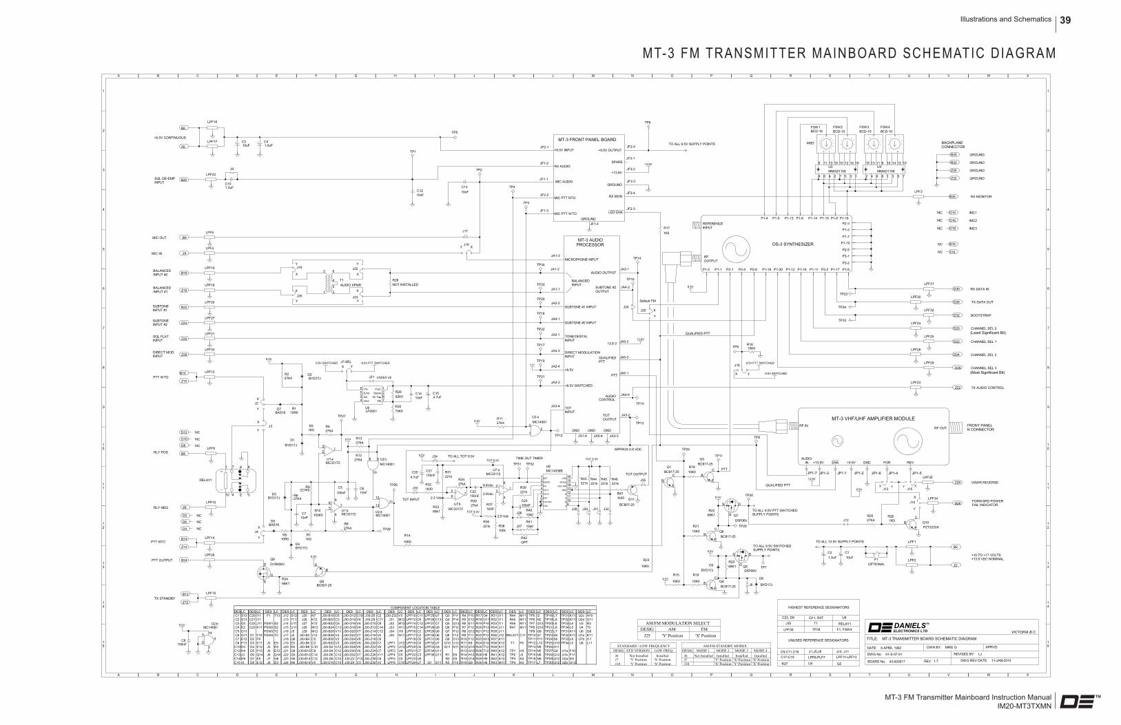
MT-3 FM Transmitter Mainboard Instruction Manual IM20-MT3TXMN
Illustrations and Schematics 39
mt-3 fm tranSmItter maInBoard SCHematIC dIaGram
AM/FM STANDBY MODES
J6J7
Not Installed Installed'Y' Position
DESIG MODE 1 MODE 2
J18 'X' Position
Installed'X' Position
MODE 3
'Y' Position
Installed'X' Position
MODE 4
'X' Position
STANDARD / LOW FREQUENCY
J6J7
Not Installed'Y' Position
Installed'X' Position
DESIG STD VERSION LOW FREQ.
J18 'Y' Position 'X' Position
AM/FM MODULATION SELECT
J25 'Y' Position 'X' PositionDESIG AM FM
DES LC DES LC DES LC DES LC DES LC DES LC DES LC DES LC DES LC DES LC DES LC DES LC DES LC DES LC DES LC DES LC DES LC DES LC DES LC DES LCC1 S13 C20 I11 F1 T13 J12 S12 J25 N7 J30-B18 C6 J30-D12 C10 J30-Z6 C2 J30-Z32 V3 LPF10 C11 LPF25 U7 Q3 P11 R4 F10 R17 O4 R31 I11 R44 M11 TP5 I2 TP18 L7 TP31 K11 U2c H10C2 S13 C21 I11 J13 T11 J26 K12 J30-B20 C3 J30-D14 V4 J30-Z8 C11 J31 M12 LPF12 C8 LPF26 C13 Q4 P14 R5 E12 R18 O11 R32 I11 R45 M11 TP6 N2 TP19 L8 TP32 K11 U2d G11C3 D2 C22 J11 FSW1 S2 J14 U11 J27 K12 J30-B22 C6 J30-D16 V4 J30-Z10 C8 J32 M12 LPF14 C12 LPF27 C7 Q5 Q13 R6 E11 R19 P14 R33 I11 R46 M11 TP7 Q13 TP20 L6 TP33 L6 U3 R3C4 E2 C23 K11 FSW2 S2 J15 U11 J28 M12 J30-B24 C13 J30-D18 V4 J30-Z12 C14 J33 H11 LPF15 C14 LPF28 U8 Q6 P12 R7 F12 R20 P13 R34 J11 R47 M11 TP8 Q10 TP21 L8 TP34 L5 U4 T3C5 G11 FSW3 T2 J16 J5 J29 M12 J30-B26 V11 J30-D20 V7 J30-Z14 C12 J34 I10 LPF16 C2 LPF29 U8 Q7 P12 R8 G12 R21 P12 R35 J11 TP9 Q8 TP22 L7 TP31 K11 U6 G8C6 G11 D1 F10 FSW4 T2 J17 J5 J30-B2 V12 J30-B28 V4 J30-D22 V7 J30-Z16 V5 J35 N11 LPF17 C2 LPF30 U6 Q8 F13 R9 F11 R22 P12 R36 J12 RELAY1 C11 TP10 S7 TP23 S6 TP32 K11 U7a K11C7 E12 D2 F8 J18 Q8 J30-B4 C5 J30-B30 V3 J30-D24 V8 J30-Z18 C6 LPF18 C6 LPF31 U6 Q9 D13 R10 F12 R23 N13 R37 K11 TP11 P11 TP24 S6 TP33 L6 U7b I11C8 F13 D3 E11 J2 E9 J19 E5 J30-B6 C2 J30-B32 V3 J30-D26 V8 J30-Z20 C7 LPF1 U12 LPF19 C6 LPF32 U7 Q10 U12 R11 K9 R24 E14 R38 K12 T1 F6 TP12 L10 TP25 O10 TP34 L5 U8 L11C10 D3 D4 E12 J3 E9 J20 E6 J30-B8 C10 J30-D2 C12 J30-D28 V6 J30-Z22 V8 LPF2 U13 LPF20 C6 LPF33 C8 Q11 N11 R12 G10 R25 T12 R39 K11 TP13 N9 TP26 H11C12 H4 D5 P13 J4 E12 J21 G8 J30-B10 C8 J30-D4 C12 J30-D30 V6 J30-Z24 C7 LPF3 U4 LPF21 C7 LPF34 U11 R13 G10 R26 T12 R40 K12 TP1 H3 TP14 N5 TP27 G9 U1a F10C13 J3 D6 Q14 J6 Q14 J22 G5 J30-B12 C14 J30-D6 C12 J30-D32 V7 J30-Z26 V11 LPF4 C5 LPF22 C3 LPF35 U11 R1 E9 R14 H12 R28 H6 R41 K12 TP2 J3 TP15 N9 TP28 G12 U1b F11C14 H9 D7 E9 J7 G8 J23 G6 J30-B14 C12 J30-D8 C10 J30-Z2 V13 J30-Z28 C8 LPF5 C5 LPF23 U8 R2 E8 R15 O14 R29 H9 R42 K12 TP3 K4 TP16 N6 TP29 Q12 U2a K9C15 I9 D8 E12 J9 D3 J24 N6 J30-B16 V5 J30-D10 C10 J30-Z4 C5 J30-Z30 V3 LPF8 C10 LPF24 U7 Q1 O11 R3 F10 R16 Q8 R30 H9 R43 M11 TP4 K3 TP17 L7 TP30 Q12 U2b G13
COMPONENT LOCATION TABLE
danielselecTronics lTd
TM
VICTORIA B.C.
DWG No: 01-S-07-01 REVISED BY: LJ
DWG REV DATE: 11-JAN-2010
XIWV IIUT IISR IIQP IION IIML IIKJ IIIH IIGF IIED IICIBA I
15
15
14
__
13
12
__
__
11
__
10
__
9
8
__
__
7
__
6
5
__
__
4
3
__
__
2
__
1
__
XIWV IIUT IISR IIQP IION IIML IIKJ IIIH IIGF IIEIDC IB IA I
1
__
2
__
3
__
4
__
5
__
6
__
7
__
8
__
9
__
10
__
11
__
12
__
13
__
14
__
(Most Significant Bit)
(Least Significant Bit)
5
DWN BY: MIKE G
Default FM
UNUSED REFERENCE DESIGNATORS
REV: 1.7BOARD No: 43-920917
APRVD:DATE: 8 APRIL 1992
TITLE: MT-3 TRANSMITTER BOARD SCHEMATIC DIAGRAM
Q2U5R27
LPF11-LPF13LPF6-PLF7C17-C19J10, J11J1,J5,J8C9,C11,C16
TP34 F1, FSW4LPF35
RELAY1T1J35
U8Q11, R47C23, D8
HIGHEST REFERENCE DESIGNATORS
Y
X
NC
NC
NC
X
TIME OUT TIMER
APPROX 0.8 VDC
JF3-4
JF3-3
JF3-2
JF3-1
JP1-7
X
Y
X
Y
X
Y
X
Y
X
Y
JP1-5JP1-4JP1-6JP1-2JP1-1JP1-3
X Y
Y
X
Y
X Y XY
UNDER U6
X
Y
X
Y
XY
JA5-1
JA5-2
JA5-3
JA5-4
JA2-4
JA3-1
JA4-2
JA3-2
JA4-4
JA1-4 JA3-3
JF2-3
JF2-4
JF1-4
JA3-4
JA2-3
JA4-3
JA4-1
JA2-1
JA2-2
JA1-1
JA1-2
JA1-3
JF1-1
JF1-3
JF2-2
JF1-2
JF2-1
FRONT PANELN CONNECTOR
BACKPLANE CONNECTOR
LPF16
LPF17
LPF22
LPF5
LPF4
LPF19
LPF18
LPF20
LPF27
LPF21
LPF33
LPF12
LPF8
LPF10
LPF14
LPF26
LPF15
Z12
B12TX STANDBY
B24PTT OUTPUT
Z14
B14PTT NTO
D4 NC
D6 NC
D2 NC
B8RLY POS
D8 NC
D10 NC
D12 NC
Z10
B10PTT WTO
Z28DIRECT MODINPUT
Z20SQL FLATINPUT
Z24SUBTONEINPUT #2
B22SUBTONEINPUT #1
Z18BALANCEDINPUT #1
B18BALANCEDINPUT #2
Z4MIC IN
B4MIC OUT
B20SQL DE-EMPINPUT
Z6
B6
+9.5V CONTINUOUS
B30 GROUND
B32 GROUND
Z32 GROUND
D14 IMC1
D16 IMC2
D18 IMC3
B16NC
Z16NC
B28 RX MONITOR
D30 RX DATA IN
D28 TX DATA OUT
D32 BOOTSTRAP
D20 CHANNEL SEL 0
D22 CHANNEL SEL 1
D24 CHANNEL SEL 2
D26 CHANNEL SEL 3
Z22 TX AUDIO CONTROL
Z26 VSWR REVERSE
B26FORWARD POWERFAIL INDICATOR
B2
+10 TO +17 VOLTS+13.8 VDC NOMINAL
Z2LPF2
LPF1
LPF34
LPF35
LPF23
LPF29
LPF28
LPF25
LPF24
LPF32
LPF31
LPF30
C310uF
C41.0uF
TP5
TP2
TP4
TP3
TP1
C1310nF
TP6
C101.0uF
J9
J16
J17
TP20
TP18
TP22
TP17
TP19
TP21
R28NOT INSTALLED
R227K4
D2BYD17J
D1BYD17J
1 9 87
4 3210
RELAY1
J4
D7BAS16
R110R0
R427K4
R31K0
TP27
23
1
U1aMC33172
4
56
78
U1 bMC33172
D3BYD17J
R627K4
D4BYD17J
D8BAS16
R510R0
R71K0
R827K4
C610nF
R10100K0
R9221K0
TP26
8 9
10
U2 cMC14081
13
1211
U2 dMC14081
1
23
U2 aMC14081
G
D
S
Q9D15N06V E
BC
Q8BC807-25
R1810K0
TP11
EB
C
Q1BC817-25
EB
C
Q3BC817-25
EB
CQ4BC817-25
D5BYD17J
D6
BYD17JJ6
TP7G
DS
Q5D5P06V
J21
R3015K0
9.5V
C1410nF
R2982K5
C154.7uF
J15J13
J14
EB
CQ10PZT2222A
R261K0
R2527K4J12
TP8
TP15
TP9
TP16
TP14
R171K0
J18
R1610K0
TP23
TP24
TP10
J7-SEL
TO ALL 9.5V PTT SWITCHEDSUPPLY POINTS
MICROPHONE INPUT
BALANCEDINPUT
+9.5V
+8.0V SWITCHED
TONE/DIGITALINPUT
AUDIO OUTPUT
SUBTONE #1 INPUT
SUBTONE #2 INPUT
DIRECT MODULATIONINPUT
AUDIO
SUBTONE #2OUTPUT
TOTINPUT
TOTOUTPUT
GND GND
MT-3 AUDIOPROCESSOR
13.8 V
QUALIFIEDPTT
PTT
GND
CONTROL
2
1
6
4
3
T1AUDIO XFMR
C1210nF
R1327K4
R1227K4
R1127K4
R19
10K0
R15
10K0
R14
10K0
R23
10K0
R2468K1
C5100nF
C710nF
J20
J22
J23
J24
J19
J25
RF INRF OUT
+9.5V+13.8V ENA GND FOR REV
OR
MT-3 VHF/UHF AMPLIFIER MODULE
AUDIOIN
LPF3
Z8RLY NEG
TP30
G
DS
Q7D5P06V
R2110K0
C22100nF
R39221k
100nFC23
R44221k
R45221k
R46221k
R43221k
R4115k0
R3527k4R33
68k1
R31221k
R321k00
R36221k
R3427k4
R38100k
R371k00
R42OPT
C21100nF
32
8
4
1
U7MC33172
a
BC807-25Q11
SET
RESET
IN1
OUT1
OUT2
BYP
CLK INH
VSS
VDD
MONO
OSC INH
DEC
D
C
B
A
12345678
161514131211109
U8MC14536B
TP25
56
7
bU7MC33172
C204.7uF
R471k00
R4010k0
TO ALL TOT 9.5V
TP12
TP31 TP32
TP13
TP33
TP34
Z30 GROUND
13572468
9 11 13 15 10 12 14 16
MMAD1108U3
75318642
15 13 11 9 16 14 12 10
MMAD1108U4
J2
J3
TO ALL 13.8V SUPPLY POINTS
C110uF
C21.0uF
TO ALL 9.5V SWITCHEDSUPPLY POINTS
R2068K1 OPTIONAL
F1
R2268K1
EB
CQ6BC817-25
TP29
TO ALL 9.5V SUPPLY POINTS
+9.5V INPUT +9.5V OUTPUT
LED ENA
GROUNDMIC PTT WTO
MIC PTT NTO
MIC AUDIO
MT-3 FRONT PANEL BOARD
RX AUDIOSPARE
+13.8V
GROUND
RX MON
8
F 10
2
3
4
5
679
A
B
C
D
E
MSD
FSW1BCD-16
5
01
2
3
46
7
8
9
BCD-10FSW2
5
01
2
3
46
7
8
9
BCD-10FSW3
5
01
2
3
46
7
8
9
BCD-10FSW4
C8100nF
5
64
14
7
U2 bMC14081
TP28
J29J28 J32J31
J33
J34
J35
J26
J27
P1-18 P1-20 P1-12 P1-19 P1-11 P2-2 P1-17 P1-9
P3-2
P3-1
P2-5
P1-10
P1-7
P1-3
P2-3P1-16P1-8P1-15P1-14P1-6P1-13P1-5P1-4
P1-2 P1-1 P2-1 P2-4 P2-6
RFOUTPUT
REFERENCEINPUT
OS-3 SYNTHESIZER
9.5V PTT SWITCHED9.5V SWITCHED
Vin Error Sd Gnd
Vout Sense
5V Tap FB
8534
1267
LP2951U6
9.5V
9.5V
9.5V
9.5V
9.5V
9.5V
TOT 9.5V
TOT 9.5V
TOT 9.5V
9.5V
9.5V
9.5V
9.5V
13.8V
9.5V SWITCHED
9.5V PTT SWITCHED
13.8V
9.5V
13.8V
PTT
TOT INPUT
TOT OUTPUT
QUALIFIED PTT
QUALIFIED PTT
2.2 Vdc
9.4Vdc
2.9 Vdc
2.9Vdc

MT-3 FM Transmitter Mainboard Instruction ManualIM20-MT3TXMN
Illustrations and Schematics40
front Panel Board ComPonent layout dIaGram front Panel Board SCHematIC dIaGram
DATE: 20 NOV 97
TITLE: MT-3 FRONT PANEL BOARD
BOARD NO: 43-921212
REV DATE: 28 JUL 04DWG No: 01-T-02-01
1
11
21
2
12
22
3
13
23
4
14
24
5
15
25
6
16
26
7
17
27
8
18
28
9
19
29
10
20
30
B
+
DANIELSELECTRONICS LTD
TM A
4
3
2
1
4
3
2
1
4
3
2
1
A
P1 D1
PF3 PF2PF1
MIC
SW1c b a
f e d
J1J2
Y X
Y
X
Solder Jumper On Solder Side Of PCB.
Factory Installed Solder Jumper.
A
21436587
12
34
KEY
ED
NO
RM
TITLE:
DATE:
DWG No.:
BOARD No.:
DWN BY: APRVD:
DWG REV DATE:
REVISED BY:
REV:
DANIELSELECTRONICS LTD
TM
VICTORIA BC.SW1
PF3MIC
J2D1C1
HIGHEST REFERENCE DESIGNATORS
UNUSED REFERENCE DESIGNATORS
----------
-----
-----
-----
----------
-----
-----
----------
-----
03 JUL 03
SHANE AEBISCHER
1.243-921212
M. GAUBE07 APRIL 92
MT-3 FRONT PANEL BOARD SCHEMATIC DIAGRAM
01-S-01-01
X
Y
PF3-3
PF3-4
PF3-1
PF3-2
X
PF1-4
PF1-1
PF1-2
PF1-3
PF2-2
PF2-3
PF2-4
PF2-1
MIC-2
MIC-4
MIC-3
MIC-1
Y
KEYED
NORM
D1
J1
C1N/I
1
2
3
4
MIC
PF2
4
2
1
3
PF3
1
2
3
4
5
6
7
8P1
J2
F
E
D
C
B
A
SW1
1
2
3
4
PF1
+9.5V IN
LED ENA
MIC PTT NTO
MIC PTT WTO
MIC INPUT
MIC INPUTMIC PTT
MIC PTT
RX MONRX MON
+9.5V OUT
+9.5V OUT
RX AUDIO
RX AUDIO+13.8V
+13.8V
SPARESPARE

MT-3 FM Transmitter Mainboard Instruction Manual IM20-MT3TXMN
Illustrations and Schematics 41
fm audIo ProCeSSor Board ComPonent layout dIaGramBOTTOM SIDE
TOP SIDE
1
11
21
2
12
22
3
13
23
4
14
24
5
15
25
6
16
26
7
17
27
8
18
28
9
19
29
10
20
30
danielselecTronics lTd
TM
DATE: 19 JAN 2010
TITLE: FM AUDIO PROCESSOR BOARD - VHF LOW BAND
BOARD NO: 43-911923
REV DATE: DWG No: 03-T-01-01
- JUMPERS INSTALLED
JU41JU4
JU17JU36
JU2X Y
X
Y
JU14Y X
JU20X Y
JU27X Y
JU5
Y
X
JU1X Y
JU15X Y
JU12X Y
JU9
X
YX
JU39Y X
JU34
Y
X
JU21X Y
XJU25
Y
XJU19
X
Y
JU22
Y
X
JU6
JU8
JU32
JU31
JU18
JU37
JU38
JU29
JU7
JU23
JU28
JU13
JU10
JU16
JU33
JU11
JU42X Y
JU43
Y
X
JU44
JU45
JU26JU3Y
Y JU24
Y
X
JU35C84.7µF
P1
C264.7µF
R73N/I
R618k2
R418k2
R560R0
C510nF
R10R0
C41.0µF
R51M0
R64100k
R30604R0
R74N/I
R72k21
P2
C1010nF
R112k21
R1049k9
R82k21
R57N/I
R4049k9 R52
100k
R26N/I
R255k11
R4916k2
R1510k0
C2010nF
C36330nF
R1310k0
R2011k8R28
N/I
R81N/I
P4
C18100nF
C1710nF
R1711k8
R18N/I
R3449k9
C23330pF
R16100k0C41
10nF
R45N/I
R440R00
R53N/I
R3251k1R54
10k0
C121.0nF
R5049k9
C2410nF
C454.7µF
R351K00
R12N/I
R7949k9
R2249k9
R2149k9
R5549k9
C61µF
C211µF
P3
R580R00
R720R00
R3749k9
R7720k0
R7510k0
Q1BC817-25
R683k48
R692k00
R6616k2
R6756k2
C34.7µF
R635k0
U4LTC1569-6
R425k0
R25k0
R315k0
R385k0
R48100k0
R14N/I
R2950k0
U3MC33174
R3650k0
FB1
U5TC4S66F
U1
SA571D
C1347uF
C2947uF
C3147uF
U2
MC33174
U6TC4S66F
R8350k0
C484.7µF
C504.7µF
C42680nF
C7680nF
R23N/I
R24N/I
R8510k0
R7810k0
C4910nF
R8610k0
C27100nF
R949k9 R65
100k
R715k11
R464k53
C1410nF
C43150pF R84
10k0
R8210k0
C19330nF
R4311k8
R47100k
R3100k
R33100k
R59221K
R41137k
R5110k0
R6215k4
R7616k2
C11µF
C301µF
C91µF
C21.0µF
C251µF
C351.0µF
C39680nF
R3913k3R60
18k2R6118k2
R8027k4
C284.7µF
C511.0µF
C161.0µF
C461.0µF
C471.0µFC33
1.0µF
C2210nF
R7010k0
C44N/I
C401.0µF
R8849k9
C52150pF
C534.7µF
C54100nF
C55100nF C56
33nF
1
2
3
4
1
2
3
4
1
2
3
4
1
2
3
4
R89100R
R27-SMD10k
R19-SMDN/I
4
1
2
3
4
1
2
3
4
1
2
3
4
1
2
3
+
C383.3nF
P2 P3P4
C373.3nF
C32N/I
P1
P5
P8
P6
P7
C153.3nF
R19-THDN/I
C341.0 uF
R27-THDN/I
R1 J1R2 K3R3 H1R4 J1R5 I2R6 J2R7 H2R8 E2R9 E2R10 H2R11 G2R12 A1R13 F1R14 O3R15 F1R16 E1R17 D2R18 E2R19 Q4R20 E1R21 B2R22 A2R23 C1R24 C1R25 D2
R76 I1R77 C2R78 D1R79 C2R80 A1R81 C1R82 G2R83 S3R84 E1R85 C1R86 D1R87 M4R88 E2R89 D1
C51 F2C52 G1C53 N4C54 G2C55 A2C56 B2
FB1 K4
JU1 F1JU2 H2JU3 C1JU4 H1JU5 G1JU6 A2JU7 A1JU8 A2JU9 F2JU10 F1JU11 I1JU12 F1JU13 F1JU14 G2JU15 F1JU16 G1JU17 I2JU18 B2JU19 B1JU20 H1JU21 C2JU22 A1JU23 D1JU24 E2JU25 B1
JU26 E1JU27 H1JU28 D2JU29 B2JU30 N/AJU31 B1JU32 A2JU33 G2JU34 D2JU35 D2JU36 J2JU37 D2JU38 C1JU39 D1JU40 N/AJU41 C1JU42 H2JU43 D2JU44 B2JU45 B2
P1 L4P2 O4P3 S4P4 R4P5 Q3P6 T4P7 Q4P8 T3P9 A1P10 A1P11 B1P12 A1
Q1 C2
R26 C2R27 P3R28 E1R29 S3R30 J2R31 M3R32 C1R33 H1R34 D1R35 A1R36 T3R37 C2R38 N3R39 I1R40 F2R41 I1R42 R3R43 G1R44 D1R45 D1R46 F2R47 G1R48 O3R49 G1R50 B1
R51 I1R52 F2R53 D1R54 C1R55 B2R56 J1R57 G2R58 B1R59 I1R60 H1R61 H1R62 J1R63 N3R64 I2R65 G2R66 A2R67 A2R68 A2R69 A1R70 H2R71 G1R72 B1R73 I2R74 I2R75 C2
C26 H1C27 B2C28 S4C29 Q3C30 I1C31 R4C32 M4C33 S4C34 S3C35 I1C36 E2C37 P4C38 O4C39 G1C40 T4C41 D1C42 M4C43 E1C44 E1C45 B1C46 T4C47 T4C48 P3C49 D2C50 P3
COMPONENT LOCATION TABLE
DES LOC DES LOC DES LOC DES LOC DES LOC DES LOC DES LOC DES LOC DES LOCC1 I1C2 J1C3 O3C4 J1C5 J2C6 A2C7 L4C8 J2C9 I1C10 G2C11 N/AC12 C1C13 K4C14 F1C15 L4C16 M4C17 E1C18 F2C19 H2C20 G2C21 A1C22 H2C23 E1C24 C1C25 H1
DES LOCU1 L3U2 N3U3 R3U4 T3U5 R3U6 S3
DES LOC
TP1 F1TP2 B1TP3 I2TP4 J1TP5 C1TP6 G2TP7 D2TP8 D1TP9 C1TP10 D1TP11 I1TP12 G1TP13 H2TP14 C1
DES LOC
P10
P11
TP3
TP11TP4
TP12
TP7
TP9
TP6
TP1
TP10
TP2
P9 P5P8
P6
P12
P7
TP13
TP5
TP14
MICROPHONEINPUT LEVEL
CONTROL
BALANCEDINPUT LEVEL
CONTROL
BALANCEDCOMPRESSION
CONTROL
MICROPHONECOMPRESSION
CONTROL
AUXILIARYINPUT LEVEL
CONTROL
4.0VVOLTAGEADJUST
SUBTONE 1 INPUT LEVEL
CONTROL
DEVIATIONCONTROL
TCXODC LEVELADJUST
TCXOMODULATION
LEVEL ADJUST
INPUTDC LEVELADJUST
TP8
30 AWG WIRE JUMPER
1
2
A B C D E F G H I J
3
4
K L M N O P Q R S T
PCBTRACE CUT
R8750k0
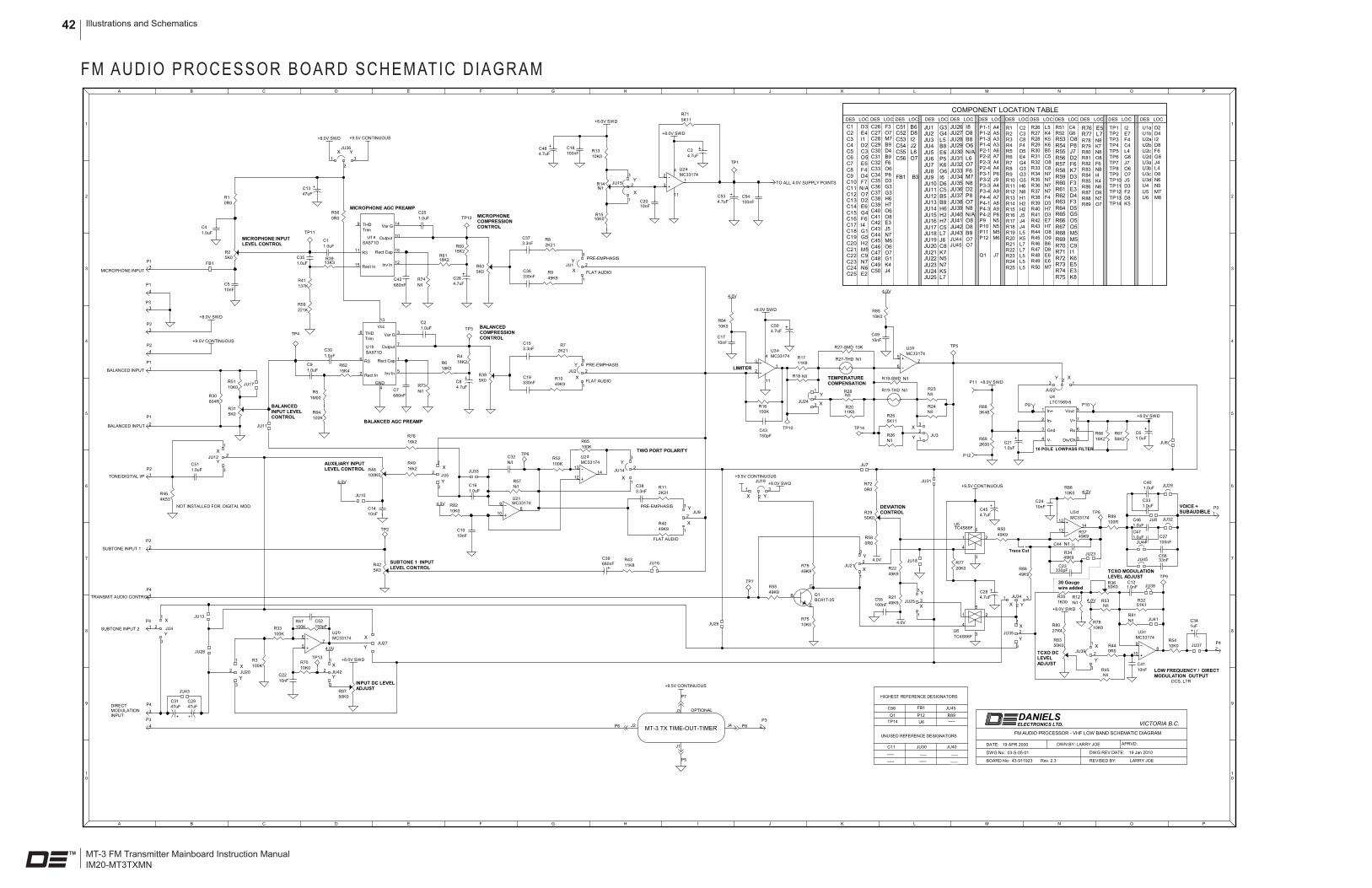
MT-3 FM Transmitter Mainboard Instruction ManualIM20-MT3TXMN
Illustrations and Schematics42
fm audIo ProCeSSor Board SCHematIC dIaGram A
A
B
B
C
C
D
D
E
E
F
F
G
G
H
H
I
I
J
J
K
K
L
L
M
M
N
N
O
O
P
P
1 1
2 2
3 3
4 4
5 5
6 6
7 7
8 8
9 9
1 10 0
R1 C2R2 C3R3 C8R4 F4R5 D5R6 E4R7 G4R8 G3R9 G3R10 G5R11 H6R12 N8R13 H1R14 H2R15 H2R16 J5R17 J4R18 J4R19 L5R20 K5R21 L7R22 L7R23 L5R24 L5R25 L5
R76 E5R77 L7R78 N8R79 K7R80 N8R81 O8R82 F6R83 N8R84 I4R85 K4R86 N6R87 D9R88 N7R89 O7
C51 B6C52 D8C53 I2C54 J2C55 L8C56 O7
FB1 B3
JU1 G3JU2 G4JU3 L5JU4 B8JU5 E6JU6 P5JU7 K6JU8 O6JU9 I6JU10 D6JU11 C5JU12 B5JU13 B8JU14 H6JU15 H2JU16 H7JU17 C5JU18 L7JU19 J6JU20 C8JU21 K7JU22 N5JU23 N7JU24 K5JU25 L7
JU26 I8JU27 D8JU28 B8JU29 O6JU30 N/AJU31 L6JU32 O7JU33 F6JU34 M7JU35 N8JU36 D2JU37 P8JU38 O7JU39 N8JU40 N/AJU41 O8JU42 D8JU43 B9JU44 O7JU45 O7
P1-1 A4P1-2 A5P1-3 A3P1-4 A3P2-1 A6P2-2 A7P2-3 A4P2-4 A4P3-1 P6P3-2 J9P3-3 A4P3-4 A9P4-4 A7P4-1 A8P4-3 A9P4-2 P8P9 N5P10 N5P11 M5P12 M6
Q1 J7
R26 L5R27 K4R28 K5R29 K6R30 B5R31 C5R32 O8R33 C8R34 N7R35 N7R36 N7R37 N7R38 F4R39 D3R40 H7R41 D3R42 E7R43 H7R44 O8R45 O9R46 B6R47 D8R48 E6R49 E6R50 M7
R51 C4R52 G6R53 O8R54 P8R55 J7R56 D2R57 F6R58 K7R59 D3R60 F3R61 E3R62 D4R63 F3R64 D5R65 G5R66 O5R67 O5R68 M5R69 M5R70 C9R71 I1R72 K6R73 E5R74 E3R75 K8
C26 F3C27 O7C28 M7C29 B9C30 D4C31 B9C32 F6C33 O6C34 P8C35 D3C36 G3C37 G3C38 H6C39 H7C40 O6C41 O8C42 E3C43 J5C44 N7C45 M6C46 O6C47 O7C48 G1C49 K4C50 J4
COMPONENT LOCATION TABLEDES LOC DES LOC DES LOC DES LOC DES LOC DES LOC DES LOC DES LOC DES LOC
C1 D3C2 E4C3 I1C4 D2C5 C3C6 O5C7 E5C8 F4C9 D4C10 F7C11 N/AC12 O7C13 D2C14 E6C15 G4C16 F6C17 I4C18 G1C19 G5C20 H2C21 M5C22 C9C23 N7C24 N6C25 E2
DES LOC
U1a D2U1b D4U2a I2U2b D8U2c F6U2d G6U3a J4U3b L4U3c O8U3d N6U4 N5U5 M7U6 M8
DES LOC
TP1 I2TP2 E7TP3 F4TP4 C4TP5 L4TP6 G6TP7 J7TP8 O6TP9 O7TP10 J5TP11 D3TP12 F2TP13 D8TP14 K5
DES LOC
HIGHEST REFERENCE DESIGNATORS
UNUSED REFERENCE DESIGNATORS
VICTORIA B.C.elecTronics lTd.daniels
FM AUDIO PROCESSOR - VHF LOW BAND SCHEMATIC DIAGRAM
DWG REV DATE: 19 Jan 2010
TP14
SUBTONE 1 INPUTLEVELCONTROL
DWG No: 03-S-05-01
TRANSMIT AUDIO CONTROL
BALANCED INPUT
VOICE+SUBAUDIBLE
TWOPORTPOLARITY
30Gaugewireadded
REVISED BY: LARRY JOE
TraceCut
BOARD No: 43-911923 Rev. 2.3
DATE: 19 APR 2000
R89
JU40C11 JU30
JU45C56
-------------------------
U6Q1 P12
FB1
-----
-----
DWN BY: LARRY JOE APRVD:
TCXOMODULATIONLEVELADJUST
TCXODCLEVELADJUST
INPUTDCLEVELADJUST
Y
X
Y
X
Y
X
Y
X
PRE-EMPHASIS
FLAT AUDIO
Y
X
Y
X
Y
X
MICROPHONECOMPRESSIONCONTROL
PRE-EMPHASIS
FLAT AUDIO
BALANCEDCOMPRESSIONCONTROL
Y
X
Y
X
DCS, LTR
TEMPERATURECOMPENSATION
LIMITER
Y
X
Y
X
Y
X
10POLELOWPASSFILTER
Y
X
Y
X
OPTIONAL
Y
X
BALANCEDAGCPREAMP
MICROPHONE AGC PREAMP
YX
AUXILIARYINPUTLEVELCONTROL
NOT INSTALLED FOR DIGITAL MOD.
+9.5V CONTINUOUS
Y
X
Y
X
Y X
YX
LOWFREQUENCY/DIRECTMODULATIONOUTPUT
DEVIATIONCONTROL
YX
DIRECTMODULATIONINPUT
BALANCED INPUT
MICROPHONE INPUTLEVELCONTROL
PRE-EMPHASIS
FLAT AUDIO
BALANCEDINPUTLEVELCONTROL
3P1
2
P1
1P1
4P1
3P3
3P2
1P2
1P4
3P4
1P3
2P4
4P4
JU37
4P2
+9.5V CONTINUOUS
C34.7uF
213
JU22
10nFC10
+9.5V CONTINUOUS
C454.7uF
C284.7uF
R464K53
100KR16
10nFC17
10nFC49
50K0R29
49K9R55
10K0R75
E
B
C
BC817-25Q1
10nFC5
5K0R2
FB1
TP1
+8.0V SWD
+8.0V SWD
+8.0V SWD
+8.0V SWD+8.0V SWD
JU6
JU31
4P3
2P3
0R0R44
N/IR45
4.7uFC48
4.7uFC50
100nFC18
1.0nFC12
10K0R54
50K0R36
1
2
3
JU5
C1347uF
R48100K0
C7680nF
C84.7uF
TP3
R3251K1
C3147uF
C2947uF
R57N/I
C32N/I
C341uF
N/IR12
Rect In
Var G
Rect Cap
Output
Inv In
R3
THDTrim
15
14
16
10
12
11
9
aSA571D
U1
C42680nF
TP12
C264.7uF
Vcc
Rect In
Var G
Rect Cap
Output
Inv In
R3
THDTrim
GND
2
3
1
7
5
6
8
13
4
bU1SA571D
JU27
+9.5V CONTINUOUS
2P2
JU16
49K9R79
JU7
R23N/I
R24N/I
R255K11
R26N/I
R28N/I
R1711K8
R18 N/I
R2011K8 In+
In-
Gnd
V-
Vout
V+
Rx
Div/Clk
1
2
3
4
8
7
6
5
LTC1569-6U4
16K2R66
56K2R67
3K48R68
2K00R69
+8.0V SWDP11
P12
P9 P10
2
3
11
1
4 aMC33174U2
9
108
cMC33174U2
2
34
1
11
aMC33174U3
6
57
bMC33174U3
N/IR19-THDN/IR73
R720R0
R580R0
1.0uFC21
1.0uFC6
49K9R37
+8.0V SWD
10nFC20
13
1214
dMC33174U2
4.0V
TO ALL 4.0V SUPPLY POINTS
4.0V
4.0V
10nFC24
R1310K0
R1510K0
4.0V
4.0V
JU23
TP5
TP6
TP7
TP8
TP9
11K8R43
680nFC39
R81N/I JU41
C4110nF
R425K0
1.0uFC35
1.0uFC1
1.0uFC9
1.0uFC30
100KR3
100KR33 100K
R47
10K0R82
3.3nFC37
10K0R84
10K0R85
10K0R86
50K0R83
N/IR53
27K4R80
+8.0V SWD
1
2
3
JU3510K0R78
16k2R49
10nFC14
4.0V
16k2R76
1.0uFC16
JU33
5K11R71
TP10
1
2
3
JU20
1.0uFC51
1
2
3
JU12
2
1
3
JU15
13K3R39
137KR41
221KR59
15K4R62
1M00R5
1.0uFC25
18K2R60 2K21
R8
49K9R9
18K2R4
18K2R6
C36330nF
2K21R7
49K9R10C19
330nF
1.0uFC2
10K0R51
2
1
3
JU1
2
1
3
JU2
2
3
1
JU39
JU11C43150pF
1
2
3JU34
JU38
N/IR14
TP11
TP4
JU10
100KR52
100KR65
3.3nFC38
2K21R11
49K9R40
2
1
3
JU14
5K0R31
604RR30
TP2
330pFC23
13
1214
dMC33174U3
10nFC22
10K0R70
JU8
C27100nF
C331.0uF
C401.0uF
C471.0uF
C461.0uF
1
2
3
JU42
6
57
bMC33174U2
50K0R87
+8.0V SWDTP13
1
2
3
JU25
49K9R22
49K9R21
1 2
3
4
5TC4S66FU5
1 2
3
4
5
TC4S66FU6
4.0V
49K9R50
49K9R88
JU43
150pFC52
1
2
3
JU4JU26
JU28
JU134.0V
R10R0
100KR64
C534.7uF 100nF
C54
100nFC55
0R0R56
TP14
4.0V
1.0uFC4
+9.5V CONTINUOUS
20K0R77JU18
JU17
1
2
3JU9
2
1 3
JU19
2
3
1
JU21JU45
R635K0
R385K0
100RR89
N/IC44
9
108
cMC33174U3
R351K00
MT-3 TX TIME-OUT-TIMER
J3
J2 J4
J1
P7
P6
P5
P8
JU29
JU32
R27-THD N/I
33nFC56
2
31
JU36
1
2
3JU24
JU44
49K9R34
+8.0V SWD
1
2
3
JU3
3.3nFC15
N/IR74
18K2R61
R19-SMD N/I
R27-SMD 10K
MICROPHONE INPUT
SUBTONE INPUT 2
SUBTONE INPUT 1
TONE/DIGITAL I/P
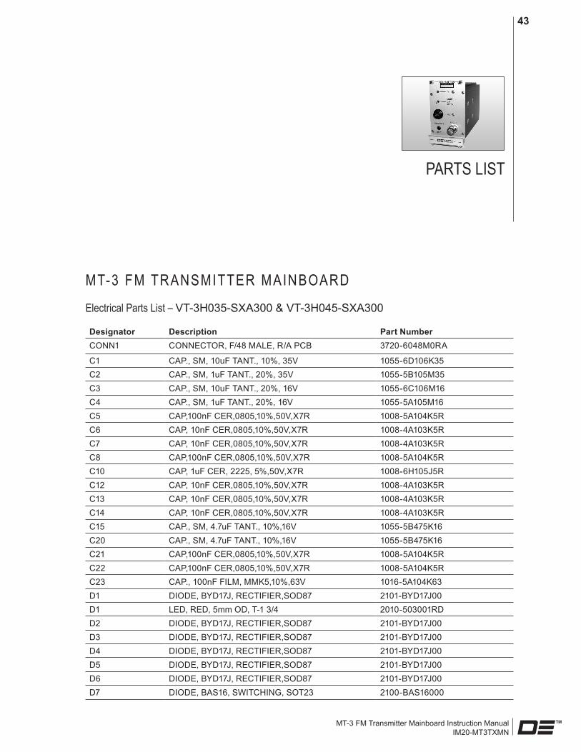
MT-3 FM Transmitter Mainboard Instruction ManualIM20-MT3TXMN
43
PartS lISt
mt-3 fm tranSmItter maInBoard
electrical Parts list – VT-3H035-SXA300 & VT-3H045-SXA300
Designator Description PartNumberCONN1 CONNECTOR, F/48 MALE, R/A PCB 3720-6048M0RA
C1 CAP., SM, 10uF TANT., 10%, 35V 1055-6D106K35C2 CAP., SM, 1uF TANT., 20%, 35V 1055-5B105M35C3 CAP., SM, 10uF TANT., 20%, 16V 1055-6C106M16C4 CAP., SM, 1uF TANT., 20%, 16V 1055-5A105M16C5 CAP,100nF CER,0805,10%,50V,X7R 1008-5A104K5RC6 CAP, 10nF CER,0805,10%,50V,X7R 1008-4A103K5RC7 CAP, 10nF CER,0805,10%,50V,X7R 1008-4A103K5RC8 CAP,100nF CER,0805,10%,50V,X7R 1008-5A104K5RC10 CAP, 1uF CER, 2225, 5%,50V,X7R 1008-6H105J5RC12 CAP, 10nF CER,0805,10%,50V,X7R 1008-4A103K5RC13 CAP, 10nF CER,0805,10%,50V,X7R 1008-4A103K5RC14 CAP, 10nF CER,0805,10%,50V,X7R 1008-4A103K5RC15 CAP., SM, 4.7uF TANT., 10%,16V 1055-5B475K16C20 CAP., SM, 4.7uF TANT., 10%,16V 1055-5B475K16C21 CAP,100nF CER,0805,10%,50V,X7R 1008-5A104K5RC22 CAP,100nF CER,0805,10%,50V,X7R 1008-5A104K5RC23 CAP., 100nF FILM, MMK5,10%,63V 1016-5A104K63D1 DIODE, BYD17J, RECTIFIER,SOD87 2101-BYD17J00D1 LED, RED, 5mm OD, T-1 3/4 2010-503001RDD2 DIODE, BYD17J, RECTIFIER,SOD87 2101-BYD17J00D3 DIODE, BYD17J, RECTIFIER,SOD87 2101-BYD17J00D4 DIODE, BYD17J, RECTIFIER,SOD87 2101-BYD17J00D5 DIODE, BYD17J, RECTIFIER,SOD87 2101-BYD17J00D6 DIODE, BYD17J, RECTIFIER,SOD87 2101-BYD17J00D7 DIODE, BAS16, SWITCHING, SOT23 2100-BAS16000

MT-3 FM Transmitter Mainboard Instruction ManualIM20-MT3TXMN
Parts List44
Designator Description PartNumberD8 DIODE, BAS16, SWITCHING, SOT23 2100-BAS16000FSW1 SWITCH, BCD-16 STEPS,5 PIN,PCB 5273-16BCD001FSW2 SWITCH, BCD-10 STEPS,5 PIN,PCB 5273-10BCD001FSW3 SWITCH, BCD-10 STEPS,5 PIN,PCB 5273-10BCD001FSW4 SWITCH, BCD-10 STEPS,5 PIN,PCB 5273-10BCD001JS1-1 SOCK. STRIP-L/P,1ROW x12PIN,Au 5016-SL112G08JS1-13 SOCK. STRIP-L/P,1ROW x 9PIN,Au 5016-SL109G08JS2-1 SOCK. STRIP-L/P,1ROW x 6PIN,Au 5016-SL106G08JS3-1 SOCK. STRIP-L/P,1ROW x 2PIN,Au 5016-SL102G08LPF1-5 FILTER, SM, EMI/LPF, 360pF,FER 1306-T361F2D5LPF8 FILTER, SM, EMI/LPF, 360pF,FER 1306-T361F2D5LFP10 FILTER, SM, EMI/LPF, 360pF,FER 1306-T361F2D5LPF12 FILTER, SM, EMI/LPF, 360pF,FER 1306-T361F2D5LPF14-35 FILTER, SM, EMI/LPF, 360pF,FER 1306-T361F2D5PCB PCB, MT-3 TRANSMITTER, MAIN 4321-10920917PCB PCB, MT-3 TX, FRONT PANEL,V1.2 4321-40921212
PF1 HEADER, .1”, R/A, 2 ROW X 2PIN 5010-H202RA9TPF2 HEADER, .1”, R/A, 2 ROW X 2PIN 5010-H202RA9TPF3 HEADER, .1”, R/A, 2 ROW X 2PIN 5010-H202RA9TQ1 TRANSISTOR, BC817-25,NPN,SOT23 2120-BC817025Q3 TRANSISTOR, BC817-25,NPN,SOT23 2120-BC817025Q4 TRANSISTOR, BC817-25,NPN,SOT23 2120-BC817025Q5 MOSFET, D5P06V, P-CHAN., D-PAK 2144-D5P06V00Q6 TRANSISTOR, BC817-25,NPN,SOT23 2120-BC817025Q7 MOSFET, D5P06V, P-CHAN., D-PAK 2144-D5P06V00Q8 TRANSISTOR, BC807-25,PNP,SOT23 2120-BC807025Q9 MOSFET, D15N06V, N-CHAN., DPAK 2144-D15N06V0Q10 TRANSISTOR, PZT2222A,NPN,ST223 2120-PZT2222AQ11 TRANSISTOR, BC807-25,PNP,SOT23 2120-BC807025R1 RES., SM, 10R0 0805, 1%,100ppm 1150-1A10R0FPR2 RES., SM, 27K4 0805, 1%,100ppm 1150-4A2742FPR3 RES., SM, 1K00 0805, 1%,100ppm 1150-3A1001FPR4 RES., SM, 27K4 0805, 1%,100ppm 1150-4A2742FPR5 RES., SM, 10R0 0805, 1%,100ppm 1150-1A10R0FPR6 RES., SM, 27K4 0805, 1%,100ppm 1150-4A2742FPR7 RES., SM, 1K00 0805, 1%,100ppm 1150-3A1001FPR8 RES., SM, 27K4 0805, 1%,100ppm 1150-4A2742FPR9 RES., SM, 221K 0805, 1%,100ppm 1150-5A2213FPR10 RES., SM, 100K 0805, 1%,100ppm 1150-5A1003FPR11 RES., SM, 27K4 0805, 1%,100ppm 1150-4A2742FPR12 RES., SM, 27K4 0805, 1%,100ppm 1150-4A2742FP
mt-3 fm transmitter mainboard electrical Parts (Continued)

MT-3 FM Transmitter Mainboard Instruction ManualIM20-MT3TXMN
Parts List 45
Designator Description PartNumberR13 RES., SM, 27K4 0805, 1%,100ppm 1150-4A2742FPR14 RES., SM, 10K0 0805, 1%,100ppm 1150-4A1002FPR15 RES., SM, 10K0 0805, 1%,100ppm 1150-4A1002FPR16 RES., SM, 10K0 0805, 1%,100ppm 1150-4A1002FPR17 RES., SM, 1K00 0805, 1%,100ppm 1150-3A1001FPR18 RES., SM, 10K0 0805, 1%,100ppm 1150-4A1002FPR19 RES., SM, 10K0 0805, 1%,100ppm 1150-4A1002FPR20 RES., SM, 68K1 0805, 1%,100ppm 1150-4A6812FPR21 RES., SM, 10K0 0805, 1%,100ppm 1150-4A1002FPR22 RES., SM, 68K1 0805, 1%,100ppm 1150-4A6812FPR23 RES., SM, 10K0 0805, 1%,100ppm 1150-4A1002FPR24 RES., SM, 68K1 0805, 1%,100ppm 1150-4A6812FPR25 RES., SM, 27K4 0805, 1%,100ppm 1150-4A2742FPR26 RES., SM, 1K00 0805, 1%,100ppm 1150-3A1001FPR29 RES., SM, 82K5 0805, 1%,100ppm 1150-4A8252FPR30 RES., SM, 15K0 0805, 1%,100ppm 1150-4A1502FPR31 RES., SM, 221K 0805, 1%,100ppm 1150-5A2213FPR32 RES., SM, 1K00 0805, 1%,100ppm 1150-3A1001FPR33 RES., SM, 68K1 0805, 1%,100ppm 1150-4A6812FPR34 RES., SM, 27K4 0805, 1%,100ppm 1150-4A2742FPR35 RES., SM, 27K4 0805, 1%,100ppm 1150-4A2742FPR36 RES., SM, 221K 0805, 1%,100ppm 1150-5A2213FPR37 RES., SM, 1K00 0805, 1%,100ppm 1150-3A1001FPR38 RES., SM, 100K 0805, 1%,100ppm 1150-5A1003FPR39 RES., SM, 221K 0805, 1%,100ppm 1150-5A2213FPR40 RES., SM, 10K0 0805, 1%,100ppm 1150-4A1002FPR41 RES., SM, 15K0 0805, 1%,100ppm 1150-4A1502FPR43 RES., SM, 221K 0805, 1%,100ppm 1150-5A2213FPR44 RES., SM, 221K 0805, 1%,100ppm 1150-5A2213FPR45 RES., SM, 221K 0805, 1%,100ppm 1150-5A2213FPR46 RES., SM, 221K 0805, 1%,100ppm 1150-5A2213FPR47 RES., SM, 1K00 0805, 1%,100ppm 1150-3A1001FPRELAY1 RELAY, 9VDC, 2 FORM C,PCB MNT. 5310-2C09P005SW1 SWITCH, TOG/DPDT,O-O-O,PCB/STR 5215-T2031V02T1 TRANSFORMER, AUDIO,600R,1:1 1280-600P6005U1 IC, MC33172, DUAL OP AMP, SO-8 2302-33172N08U2 IC, 4081, QUAD 2I/P AND, SO-14 2375-40810N14U3 IC, MMAD1108,8 DIODE/ARY.,SO16 2331-11080N16U4 IC, MMAD1108,8 DIODE/ARY.,SO16 2331-11080N16U6 IC, LP2951,PROG. VOLT REG,SO-8 2305-29510N08U7 IC, MC33172, DUAL OP AMP, SO-8 2302-33172N08U8 IC, 4536, PROG. TIMER, SO-16L 2375-45360W16
mt-3 fm transmitter mainboard electrical Parts (Continued)

MT-3 FM Transmitter Mainboard Instruction ManualIM20-MT3TXMN
Parts List46
mt-3 fm transmitter mainboard mechanical Parts listVT-3H035-SXA300 & VT-3H045-SXA300
Description PartNumber Qty. UOMCABLE, CONFORM., 31mm/5mm/4mm 7489-C1079100 1 EACASE, 14HP RF PLUG-IN, MT-3 TX 3702-62502010 1 EACONN., N JACK, PANEL MNT,C/SNK 5184-10923011 1 EACONNECTOR, MIC., 4 PIN, MALE 5040-114ST0BK 1 EAFASTENER, QUICK RELEASE, GRAY 3702-10000120 4 EAFERRITE, BEAD,43MIX,3x3.5mm OD 1210-43030350 3GASKET, BeCu,3FINGER,.71”,CLIP 5630-12023250 2 EAHANDLE, FRONT PANEL, 14HP,GREY 3702-10000614 1 EAHOLE PLUG, .250” HOLE,NYL.,BLK 5671-250N062B 1 EALABEL/LEXAN, 14HP, VHF: ORANGE 3536-10101405 1 LBLLOCKWASHER, M3, SPLIT,A2 STEEL 5814-3M0LK00S 4 EANAMEPLATE, BLANK, 14HP, ALUM. 3702-10001214 1 EANUT, M2.5, HEX, 5.0mm FLATS,A2 (for CONN1) 5813-2M5HX50S 2 EANUT, M2.5, SQUARE-5mm, ZINC 5813-2M5SQ50Z 2 EAPANEL, REAR,POS.4,14HP EXTRSN. 3702-63002101 1 EAPANEL/FRNT,W/IDENT:TX-EXTR.VER 3802-61002101 1 EASCREW, M2 X 4, PAN/PHILLIPS,A2 5812-2M0PP04S 6 EASCREW, M2.5 x 10 PAN/PHIL, A2 (for CONN1) 5812-2M5PP10S 2 EASCREW, M2.5 x 14 FLAT/PHIL, A2 5812-2M5FP14S 2 EASCREW, M3 X 6, FLAT/PHIL., A2 5812-3M0FP06S 4 EA
SCREW, M3 X 6, PAN/PHILLIPS,A2 5812-3M0PP06S 4 EASCREW, M3 x 6,OVAL C/S/PHIL,A2 5812-3M0VP06S 2 EASCREW, M3 x 8, PAN/PHIL, BLACK 5812-3M0PP08T 4 EASCREW, M3 x 8,OVAL C/S/PHIL,A2 5812-3M0VP08S 2 EASCREW, M3 x10,OVAL C/S/PHIL,A2 5812-3M0VP10S 2 EASCREW, M5 x 8, FLAT/PHIL., A2 5812-5M0FP08S 4 EA

MT-3 FM Transmitter Mainboard Instruction ManualIM20-MT3TXMN
Parts List 47
front Panel Board
electrical and mechanical Parts list
Designator Description PartNumberD1 LED, RED, 5mm OD, T-1 3/4 2010-503001RD
SPACER, LED-T1 3/4, .300”H,NYL 5620-503S300NPCB PCB, MT-3 TX, FRONT PANEL,V1.2 4321-40921212PF1 HEADER, .1”, R/A, 2 ROW X 2PIN 5010-H202RA9TPF2 HEADER, .1”, R/A, 2 ROW X 2PIN 5010-H202RA9TPF3 HEADER, .1”, R/A, 2 ROW X 2PIN 5010-H202RA9TSW1 SWITCH, TOG/DPDT,O-O-O,PCB/STR 5215-T2031V02
WASHER, TFE,0.036ID,1/8OD,.02T (Qty. 2) 5805-T3612F20
fm audIo ProCeSSorelectrical Parts list – A21-VUAP3
Designator Description PartNumberC1 CAP,1uF C,1206,+80-20%,25V,X7R 1008-6B105Z3RC2 CAP,1uF C,1206,+80-20%,25V,X7R 1008-6B105Z3RC3 CAP., SM, 4.7uF TANT., 10%,16V 1055-5B475K16C4 CAP,1uF C,1206,+80-20%,25V,X7R 1008-6B105Z3RC5 CAP, 10nF CER,0805,10%,50V,X7R 1008-4A103K5RC6 CAP., SM, 1uF TANT., 20%, 16V 1055-5A105M16C7 CAP,680nF CER,1206,20%,25V,X7R 1008-5B684M3RC8 CAP., SM, 4.7uF TANT., 10%,16V 1055-5B475K16C9 CAP,1uF C,1206,+80-20%,25V,X7R 1008-6B105Z3RC10 CAP, 10nF CER,0805,10%,50V,X7R 1008-4A103K5RC12 CAP, 1nF CER, 0805,10%,50V,X7R 1008-3A102K5RC13 CAP., SM, 47uF TANT., 20%, 16V 1055-6D476M16C14 CAP, 10nF CER,0805,10%,50V,X7R 1008-4A103K5RC15 CAP., 3.3nF FILM, MMK5,10%,63V 1016-3A332K63C16 CAP,1uF C,1206,+80-20%,25V,X7R 1008-6B105Z3RC17 CAP, 10nF CER,0805,10%,50V,X7R 1008-4A103K5RC18 CAP,100nF CER,0805,10%,50V,X7R 1008-5A104K5RC19 CAP,330nF CER,0805,20%,25V,X7R 1008-5A334M3RC20 CAP, 10nF CER,0805,10%,50V,X7R 1008-4A103K5RC21 CAP., SM, 1uF TANT., 20%, 16V 1055-5A105M16C22 CAP, 10nF CER,0805,10%,50V,X7R 1008-4A103K5RC23 CAP,330pF CER,0805,5%,100V,C0G 1008-2A331J1GC24 CAP, 10nF CER,0805,10%,50V,X7R 1008-4A103K5RC25 CAP,1uF C,1206,+80-20%,25V,X7R 1008-6B105Z3R

MT-3 FM Transmitter Mainboard Instruction ManualIM20-MT3TXMN
Parts List48
Designator Description PartNumberC26 CAP., SM, 4.7uF TANT., 10%,16V 1055-5B475K16C27 CAP,100nF CER,0805,10%,50V,X7R 1008-5A104K5RC28 CAP., SM, 4.7uF TANT., 10%,16V 1055-5B475K16C29 CAP., SM, 47uF TANT., 20%, 16V 1055-6D476M16C30 CAP,1uF C,1206,+80-20%,25V,X7R 1008-6B105Z3RC31 CAP., SM, 47uF TANT., 20%, 16V 1055-6D476M16C33 CAP,1uF C,1206,+80-20%,25V,X7R 1008-6B105Z3RC34 CAP., 1uF DIP. TANT., 20%, 35V 1054-5A105M35C35 CAP,1uF C,1206,+80-20%,25V,X7R 1008-6B105Z3RC36 CAP,330nF CER,0805,20%,25V,X7R 1008-5A334M3RC37 CAP., 3.3nF FILM, MMK5,10%,63V 1016-3A332K63C38 CAP., 3.3nF FILM, MMK5,10%,63V 1016-3A332K63C39 CAP., SM, 680nF TANT., 10%,35V 1055-4B684K35C40 CAP,1uF C,1206,+80-20%,25V,X7R 1008-6B105Z3RC41 CAP, 10nF CER,0805,10%,50V,X7R 1008-4A103K5RC42 CAP,680nF CER,1206,20%,25V,X7R 1008-5B684M3RC43 CAP,150pF CER,0805,5%,100V,C0G 1008-2A151J1GC45 CAP., SM, 4.7uF TANT., 10%,16V 1055-5B475K16C46 CAP,1uF C,1206,+80-20%,25V,X7R 1008-6B105Z3RC47 CAP,1uF C,1206,+80-20%,25V,X7R 1008-6B105Z3RC48 CAP., SM, 4.7uF TANT., 10%,16V 1055-5B475K16C49 CAP, 10nF CER,0805,10%,50V,X7R 1008-4A103K5RC50 CAP., SM, 4.7uF TANT., 10%,16V 1055-5B475K16C51 CAP,1uF C,1206,+80-20%,25V,X7R 1008-6B105Z3RC52 CAP,150pF CER,0805,5%,100V,C0G 1008-2A151J1GC53 CAP., SM, 4.7uF TANT., 10%,16V 1055-5B475K16C54 CAP,100nF CER,0805,10%,50V,X7R 1008-5A104K5RC55 CAP,100nF CER,0805,10%,50V,X7R 1008-5A104K5RC56 CAP, 33nF CER,0805,10%,50V,X7R 1008-4A333K5RFB1 FERRITE BEAD, SM,43MIX,.18x.12 1213-43181200P1 HEADER, .1”, R/A, 2 ROW X 2PIN 5010-H202RA9TP2 HEADER, .1”, R/A, 2 ROW X 2PIN 5010-H202RA9TP3 HEADER, .1”, R/A, 2 ROW X 2PIN 5010-H202RA9TP4 HEADER, .1”, R/A, 2 ROW X 2PIN 5010-H202RA9TPCB PCB, AUDIO PROCESSOR, MT-3 TX 4321-30911923Q1 TRANSISTOR, BC817-25,NPN,SOT23 2120-BC817025R1 RES., SM, ZERO OHM JUMPER,0805 1150-0A0R0000R2 POT.,SM/4mmSQ,5K0,MUL/TRN,SIDE 1174-DM2502J0R3 RES., SM, 100K 0805, 1%,100ppm 1150-5A1003FPR4 RES., SM, 18K2 0805, 1%,100ppm 1150-4A1822FPR5 RES., SM, 1M00 0805, 1%,100ppm 1150-6A1004FPR6 RES., SM, 18K2 0805, 1%,100ppm 1150-4A1822FPR7 RES., SM, 2K21 0805, 1%,100ppm 1150-3A2211FP
fm audio Processor electrical Parts (Continued)

MT-3 FM Transmitter Mainboard Instruction ManualIM20-MT3TXMN
Parts List 49
fm audio Processor electrical Parts (Continued)
Designator Description PartNumberR8 RES., SM, 2K21 0805, 1%,100ppm 1150-3A2211FPR9 RES., SM, 49K9 0805, 1%,100ppm 1150-4A4992FPR10 RES., SM, 49K9 0805, 1%,100ppm 1150-4A4992FPR11 RES., SM, 2K21 0805, 1%,100ppm 1150-3A2211FPR13 RES., SM, 10K0 0805, 1%,100ppm 1150-4A1002FPR15 RES., SM, 10K0 0805, 1%,100ppm 1150-4A1002FPR16 RES., SM, 100K 0805, 1%,100ppm 1150-5A1003FPR17 RES., SM, 11K8 0805, 1%,100ppm 1150-4A1182FPR21 RES., SM, 49K9 0805, 1%,100ppm 1150-4A4992FPR22 RES., SM, 49K9 0805, 1%,100ppm 1150-4A4992FPR25 RES., SM, 5K11 0805, 1%,100ppm 1150-3A5111FPR27 THERMISTOR/SMT, 10K, NTC, 1206 1185-4B103AAKR29 POT.,SM/4mmSQ,50K,MUL/TRN,SIDE 1174-DM3503J0R30 RES., SM, 604R 0805, 1%,100ppm 1150-2A6040FPR31 POT.,SM/4mmSQ,5K0,MUL/TRN,SIDE 1174-DM2502J0R32 RES., SM, 51K1 0805, 1%,100ppm 1150-4A5112FPR33 RES., SM, 100K 0805, 1%,100ppm 1150-5A1003FPR34 RES., SM, 49K9 0805, 1%,100ppm 1150-4A4992FPR35 RES., SM, 1K00 0805, 1%,100ppm 1150-3A1001FPR36 POT.,SM/4mmSQ,50K,MUL/TRN,SIDE 1174-DM3503J0R37 RES., SM, 49K9 0805, 1%,100ppm 1150-4A4992FPR38 POT.,SM/4mmSQ,5K0,MUL/TRN,SIDE 1174-DM2502J0R39 RES., SM, 15K4 0805, 1%,100ppm 1150-4A1542FPR40 RES., SM, 49K9 0805, 1%,100ppm 1150-4A4992FPR41 RES., SM, 137K 0805, 1%,100ppm 1150-5A1373FPR42 POT.,SM/4mmSQ,5K0,MUL/TRN,SIDE 1174-DM2502J0R43 RES., SM, 11K8 0805, 1%,100ppm 1150-4A1182FPR44 RES., SM, ZERO OHM JUMPER,0805 1150-0A0R0000R46 RES., SM, 4K53 0805, 1%,100ppm 1150-3A4531FPR47 RES., SM, 100K 0805, 1%,100ppm 1150-5A1003FPR48 POT.,SM/4mmSQ,100K,MUL/TN,SIDE 1174-DM4104J0R49 RES., SM, 16K2 0805, 1%,100ppm 1150-4A1622FPR50 RES., SM, 49K9 0805, 1%,100ppm 1150-4A4992FPR51 RES., SM, 10K0 0805, 1%,100ppm 1150-4A1002FPR52 RES., SM, 100K 0805, 1%,100ppm 1150-5A1003FPR54 RES., SM, 10K0 0805, 1%,100ppm 1150-4A1002FPR55 RES., SM, 49K9 0805, 1%,100ppm 1150-4A4992FPR56 RES., SM, ZERO OHM JUMPER,0805 1150-0A0R0000R58 RES., SM, ZERO OHM JUMPER,0805 1150-0A0R0000R59 RES., SM, 20K0 0805, 1%,100ppm 1150-4A2002FPR60 RES., SM, 18K2 0805, 1%,100ppm 1150-4A1822FPR61 RES., SM, 18K2 0805, 1%,100ppm 1150-4A1822FPR62 RES., SM, 15K4 0805, 1%,100ppm 1150-4A1542FP

MT-3 FM Transmitter Mainboard Instruction ManualIM20-MT3TXMN
Parts List50
fm audio Processor electrical Parts (Continued)
Designator Description PartNumberR63 POT.,SM/4mmSQ,5K0,MUL/TRN,SIDE 1174-DM2502J0R64 RES., SM, 100K 0805, 1%,100ppm 1150-5A1003FPR65 RES., SM, 100K 0805, 1%,100ppm 1150-5A1003FPR66 RES., SM, 16K2 0805, 1%,100ppm 1150-4A1622FPR67 RES., SM, 56K2 0805, 1%,100ppm 1150-4A5622FPR68 RES., SM, 3K48 0805, 1%,100ppm 1150-3A3481FPR69 RES., SM, 2K00 0805, 1%,100ppm 1150-3A2001FPR70 RES., SM, 10K0 0805, 1%,100ppm 1150-4A1002FPR71 RES., SM, 5K11 0805, 1%,100ppm 1150-3A5111FPR72 RES., SM, ZERO OHM JUMPER,0805 1150-0A0R0000R75 RES., SM, 10K0 0805, 1%,100ppm 1150-4A1002FPR76 RES., SM, 16K2 0805, 1%,100ppm 1150-4A1622FPR77 RES., SM, 20K0 0805, 1%,100ppm 1150-4A2002FPR78 RES., SM, 10K0 0805, 1%,100ppm 1150-4A1002FPR79 RES., SM, 49K9 0805, 1%,100ppm 1150-4A4992FPR80 RES., SM, 27K4 0805, 1%,100ppm 1150-4A2742FPR82 RES., SM, 10K0 0805, 1%,100ppm 1150-4A1002FPR83 POT.,SM/4mmSQ,50K,MUL/TRN,SIDE 1174-DM3503J0R84 RES., SM, 10K0 0805, 1%,100ppm 1150-4A1002FPR85 RES., SM, 10K0 0805, 1%,100ppm 1150-4A1002FPR86 RES., SM, 10K0 0805, 1%,100ppm 1150-4A1002FPR87 POT.,SM/4mmSQ,50K,MUL/TRN,SIDE 1174-DM3503J0R88 RES., SM, 49K9 0805, 1%,100ppm 1150-4A4992FPR89 RES., SM, 100R 0805, 1%,100ppm 1150-2A1000FPU1 IC, SA571D, COMPANDOR, SO-16L 2327-SA571D00U2 IC, MC33174, QUAD OP AMP,SO-14 2304-33174N14U3 IC, MC33174, QUAD OP AMP,SO-14 2304-33174N14U4 IC, LTC1569I,LPF,10TH ORD,SO-8 2326-15696N08U5 IC, 4S66F,BILATERAL SWITCH,SMV 2375-4S66FSMVU6 IC, 4S66F,BILATERAL SWITCH,SMV 2375-4S66FSMV

MT-3 FM Transmitter Mainboard Instruction ManualIM20-MT3TXMN
51
reVISIon HIStory
Revision History continued next page
Revision Date Action# Description3 Mar 02 701 TOT specification changed from 5min ± 30sec to 5min ± 50sec.3 Apr 02 697 Improve hum & noise performance, UT-3/8xxx only Version 2.3 Audio
Processor changesC56 now 22nF for 800 MHz LTR™ only (remains as 33nF for • other bands.)JU29, JU32, and JU44 Not Installed for 800 MHz LTR™•
3 Feb 02 678 To prevent frequency error when PTT first activated. Reduction of charge time for C34 on the Version 2.3 Audio Processor.C34 now 1.0µF, DIP Tantalum (was 47µF SM Tantalum)
C34 remains as 47µF for LTR™ & DCS applications.• 4 Mar 03 Reissue including Version 2.3 Audio Processor information. •
Version 1.6 Audio Processor information is removed. • Issue 4 covers Version 1.8, 2.2 & 2.3 Audio Processors. • Issue 4 contains no AM information - the document title is • changed to reflect coverage of only FM transmitters.
699 For VT-3H035 & VT-3H045 transmitters, to reduce spurious emissions for CE approval, the PCB trace pattern is modified and C44 is Not Installed.
701 Time Out Timer tolerance is changed to ±17%. Tolerance for 5 minutes setting is ± 50sec.
4-1-0 Sep 03 New Manual Format• Removed all reference to Version 1.8 Audio Processor•
4-1-1 Oct 03 Typographical updates to manual.
4-2-0 Jan 05 660 Update Audio Processor Component Layout Dwg: • 43-911923-01-T-01-01 to 43-911923-01-T-02-01 43-911923-01-S-0101 to 43-911923-01-S-02-01 Add Select table for Audio Processor Components: • “Audio Processor Component Layout Selection Table”
791 Update Main Board Component & Schematic Dwg to update J25 SEL: X installed for FM Products & Y installed for AM Products
--- Update Tx Front Panel Component Dwg: • 43-921212-01-T-01-01 to 43-921212-01-T-02-01 Update specification tables and part list•

MT-3 FM Transmitter Mainboard Instruction ManualIM20-MT3TXMN
Revision History52
Revision Date Action# Description4-2-0 (cont)
829 Update Parts List
836 Update C56 to 47nF for 950MHz transmitters.4-3-0 Jun 05 836A1 CO 836 expanded to include the UT-3/930-SXB300 Audio Processor
model selected components.836A2 CO 836 expanded to include the UT-3/930-SXB300 with this main
board.846 Update Audio Processor Component Layout and the Audio •
Processor Component Layout Selection Table. Alignment procedures updated.•
--- Revision History older than 7yrs removed from publication.• Top level mechanical parts moved to the top level Transmitter IMs; • – for all VHF Synthesized Tx mech parts consult IM20-VT3150 – for all UHF Synthesized Tx mech parts consult IM23-UT3400 – for all Crystal Tx mech parts consult IM21-xT3C
4-4-0 Dec 05 6056 OC-3 Product discontinued. Remove references.6113 VT-3/140 Audio Processor select value table updated.6115 VT-3/160 Audio Processor select value table updated.
4-5-0 Feb 06 6129 UT-3/420-SXCX00 Audio Processor select value table updated.6130 UT-3/460-SXCX00 Audio Processor select value table updated.--- Audio Processor Parts list expanded to display all models and their
band selected components.5-0-0 Feb 2010 Revisionhistoryolderthansevenyearshasbeenremoved.
6127 Improve the Low Band transmitter’s standard subtone response.6154 VHF and UHF Audio Processor Max Dev tuning change.6344 Remove all references specific to the MT-3 800/900 MHz product.6347 Discontinue the MT-3 UHF 400 and VHF 150 modules.
updated 43-920917 CLD – Top and schematic• 6437 VT-3H045 Temp compensation adjustment.
Updated the MT-3 VHF Low Band Performance Specifications• 6452 VT-3H035 Temp compensation adjustment.3682 Update operating voltage to nominal (10–17 V)•
Change document title to include MT-3• --- Update company logos and trademark information•
Apply Daniels Style Guide• Update BOMs, schematics and CLDs•
Related Documents