Product Folder Order Now Technical Documents Tools & Software Support & Community An IMPORTANT NOTICE at the end of this data sheet addresses availability, warranty, changes, use in safety-critical applications, intellectual property matters and other important disclaimers. PRODUCTION DATA. MSP430FR6047, MSP430FR60471, MSP430FR6045 MSP430FR6037, MSP430FR60371, MSP430FR6035 SLASEB7B – JUNE 2017 – REVISED DECEMBER 2017 MSP430FR604x(1), MSP430FR603x(1) Ultrasonic Sensing MSP430™ Microcontrollers for Water‑Metering Applications 1 Device Overview 1 1.1 Features 1 (1) Minimum supply voltage is restricted by SVS levels. • Best-in-Class Ultrasonic Water-Flow Measurement With Ultra-Low Power Consumption – <25-ps Differential Time-of-Flight (dTOF) Accuracy – High-Precision Time Measurement Resolution of <5 ps – Ability to Detect Low Flow Rates (<1 Liter per Hour) – Approximately 3-μA Overall Current Consumption With One Measurement per Second • Compliant to and Exceeds ISO 4064, OIML R49, and EN 1434 Accuracy Standards • Ability to Directly Interface Standard Ultrasonic Sensors (up to 2.5 MHz) • Integrated Analog Front End – Ultrasonic Sensing Solution (USS) – Programmable Pulse Generation (PPG) to Generate Pulses at Different Frequencies – Integrated Physical Interface (PHY) With Low- Impedance (4-Ω) Output Driver to Control Input and Output Channels – High-Performance High-Speed 12-Bit Sigma- Delta ADC (SDHS) With Output Data Rates up to 8 Msps – Programmable Gain Amplifier (PGA) With –6.5 dB to 30.8 dB – High-Performance Phase-Locked Loop (PLL) With Output Range of 68 MHz to 80 MHz • Metering Test Interface (MTIF) – Pulse Generator and Pulse Counter – Pulse Rates up to 1016 Pulses per Second (p/s) – Count Capacity up to 65535 (16 Bit) – Operates in LPM3.5 With 200 nA (Typical) • Low-Energy Accelerator (LEA) – Operation Independent of CPU – 4KB of RAM Shared With CPU – Efficient 256-Point Complex FFT: Up to 40× Faster Than Arm ® Cortex ® -M0+ Core • Embedded Microcontroller – 16-Bit RISC Architecture up to 16‑MHz Clock – Wide Supply Voltage Range: 1.8 V to 3.6 V (1) (2) The RTC is clocked by a 3.7-pF crystal. • Optimized Ultra-Low-Power Modes – Active Mode: Approximately 120 μA/MHz – Standby Mode With Real-Time Clock (RTC) (LPM3.5): 450 nA (2) – Shutdown (LPM4.5): 30 nA • Ferroelectric Random Access Memory (FRAM) – Up to 256KB of Nonvolatile Memory – Ultra-Low-Power Writes – Fast Write at 125 ns Per Word (64KB in 4 ms) – Unified Memory = Program + Data + Storage in One Space – 10 15 Write Cycle Endurance – Radiation Resistant and Nonmagnetic • Intelligent Digital Peripherals – 32-Bit Hardware Multiplier (MPY) – 6-Channel Internal DMA – RTC With Calendar and Alarm Functions – Six 16-Bit Timers With up to Seven Capture/Compare Registers Each – 32-Bit and 16-Bit Cyclic Redundancy Check (CRC) • High-Performance Analog – 16-Channel Analog Comparator – 12-Bit SAR ADC Featuring Window Comparator, Internal Reference, and Sample-and-Hold, up to 16 External Input Channels – Integrated LCD Driver With Contrast Control for up to 264 Segments • Multifunction Input/Output Ports – Accessible Bit-, Byte-, and Word-Wise (in Pairs) – Edge-Selectable Wake From LPM on All Ports – Programmable Pullup and Pulldown on All Ports • Code Security and Encryption – 128- or 256-Bit AES Security Encryption and Decryption Coprocessor – Random Number Seed for Random Number Generation Algorithms – IP Encapsulation Protects Memory From External Access – FRAM Provides Inherent Security Advantages

Welcome message from author
This document is posted to help you gain knowledge. Please leave a comment to let me know what you think about it! Share it to your friends and learn new things together.
Transcript
Product
Folder
Order
Now
Technical
Documents
Tools &
Software
Support &Community
An IMPORTANT NOTICE at the end of this data sheet addresses availability, warranty, changes, use in safety-critical applications,intellectual property matters and other important disclaimers. PRODUCTION DATA.
MSP430FR6047, MSP430FR60471, MSP430FR6045MSP430FR6037, MSP430FR60371, MSP430FR6035
SLASEB7B –JUNE 2017–REVISED DECEMBER 2017
MSP430FR604x(1), MSP430FR603x(1) Ultrasonic Sensing MSP430™ Microcontrollersfor Water‑‑Metering Applications
1 Device Overview
1
1.1 Features1
(1) Minimum supply voltage is restricted by SVS levels.
• Best-in-Class Ultrasonic Water-Flow MeasurementWith Ultra-Low Power Consumption– <25-ps Differential Time-of-Flight (dTOF)
Accuracy– High-Precision Time Measurement Resolution of
<5 ps– Ability to Detect Low Flow Rates (<1 Liter per
Hour)– Approximately 3-µA Overall Current
Consumption With One Measurement perSecond
• Compliant to and Exceeds ISO 4064, OIML R49,and EN 1434 Accuracy Standards
• Ability to Directly Interface Standard UltrasonicSensors (up to 2.5 MHz)
• Integrated Analog Front End – Ultrasonic SensingSolution (USS)– Programmable Pulse Generation (PPG) to
Generate Pulses at Different Frequencies– Integrated Physical Interface (PHY) With Low-
Impedance (4-Ω) Output Driver to Control Inputand Output Channels
– High-Performance High-Speed 12-Bit Sigma-Delta ADC (SDHS) With Output Data Rates upto 8 Msps
– Programmable Gain Amplifier (PGA) With–6.5 dB to 30.8 dB
– High-Performance Phase-Locked Loop (PLL)With Output Range of 68 MHz to 80 MHz
• Metering Test Interface (MTIF)– Pulse Generator and Pulse Counter– Pulse Rates up to 1016 Pulses per Second (p/s)– Count Capacity up to 65535 (16 Bit)– Operates in LPM3.5 With 200 nA (Typical)
• Low-Energy Accelerator (LEA)– Operation Independent of CPU– 4KB of RAM Shared With CPU– Efficient 256-Point Complex FFT:
Up to 40× Faster Than Arm® Cortex®-M0+ Core• Embedded Microcontroller
– 16-Bit RISC Architecture up to 16‑MHz Clock– Wide Supply Voltage Range:
1.8 V to 3.6 V (1)
(2) The RTC is clocked by a 3.7-pF crystal.
• Optimized Ultra-Low-Power Modes– Active Mode: Approximately 120 µA/MHz– Standby Mode With Real-Time Clock (RTC)
(LPM3.5): 450 nA (2)
– Shutdown (LPM4.5): 30 nA• Ferroelectric Random Access Memory (FRAM)
– Up to 256KB of Nonvolatile Memory– Ultra-Low-Power Writes– Fast Write at 125 ns Per Word (64KB in 4 ms)– Unified Memory = Program + Data + Storage in
One Space– 1015 Write Cycle Endurance– Radiation Resistant and Nonmagnetic
• Intelligent Digital Peripherals– 32-Bit Hardware Multiplier (MPY)– 6-Channel Internal DMA– RTC With Calendar and Alarm Functions– Six 16-Bit Timers With up to Seven
Capture/Compare Registers Each– 32-Bit and 16-Bit Cyclic Redundancy Check
(CRC)• High-Performance Analog
– 16-Channel Analog Comparator– 12-Bit SAR ADC Featuring Window Comparator,
Internal Reference, and Sample-and-Hold, up to16 External Input Channels
– Integrated LCD Driver With Contrast Control forup to 264 Segments
• Multifunction Input/Output Ports– Accessible Bit-, Byte-, and Word-Wise (in Pairs)– Edge-Selectable Wake From LPM on All Ports– Programmable Pullup and Pulldown on All Ports
• Code Security and Encryption– 128- or 256-Bit AES Security Encryption and
Decryption Coprocessor– Random Number Seed for Random Number
Generation Algorithms– IP Encapsulation Protects Memory From
External Access– FRAM Provides Inherent Security Advantages

2
MSP430FR6047, MSP430FR60471, MSP430FR6045MSP430FR6037, MSP430FR60371, MSP430FR6035SLASEB7B –JUNE 2017–REVISED DECEMBER 2017 www.ti.com
Submit Documentation FeedbackProduct Folder Links: MSP430FR6047 MSP430FR60471 MSP430FR6045 MSP430FR6037 MSP430FR60371
MSP430FR6035
Device Overview Copyright © 2017, Texas Instruments Incorporated
• Enhanced Serial Communication– Up to Four eUSCI_A Serial Communication
Ports– UART With Automatic Baud-Rate Detection– IrDA Encode and Decode
– Up to Two eUSCI_B Serial CommunicationPorts– I2C With Multiple-Slave Addressing
– Hardware UART or I2C Bootloader (BSL)• Flexible Clock System
– Fixed-Frequency DCO With 10 SelectableFactory-Trimmed Frequencies
– Low-Power Low-Frequency Internal ClockSource (VLO)
– 32-kHz Crystals (LFXT)– High-Frequency Crystals (HFXT)
• Development Tools and Software (Also See Toolsand Software)– Ultrasonic Sensing Design Center Graphical
User Interface– Ultrasonic Sensing Software Library– EVM430-FR6047 Water Meter Evaluation
Module Board– MSP-TS430PZ100E Target Socket Board for
100-Pin Package– Free Professional Development Environments
With EnergyTrace++ Technology– MSP430Ware™ for MSP430™ Microcontrollers
• Device Comparison Summarizes the AvailableDevice Variants and Package Options
• For Complete Module Descriptions, See theMSP430FR58xx, MSP430FR59xx, andMSP430FR6xx Family User's Guide
1.2 Applications• Ultrasonic Smart Water Meters• Ultrasonic Smart Heat Meters
• Liquid Level Sensing• Water Leak Detection
1.3 DescriptionThe Texas Instruments MSP430FR604x and MSP430FR603x family of ultrasonic sensing andmeasurement SoCs are powerful, highly integrated microcontrollers (MCUs) that are optimized for waterand heat meters. The MSP430FR604x MCUs offer an integrated Ultrasonic Sensing Solution (USS)module, which provides high accuracy for a wide range of flow rates. The USS module helps achieveultra-low-power metering combined with lower system cost due to maximum integration requiring very fewexternal components. MSP430FR604x and MSP430FR603x MCUs implement a high-speed ADC-basedsignal acquisition followed by optimized digital signal processing using the integrated Low-EnergyAccelerator (LEA) module to deliver a high-accuracy metering solution with ultra-low power optimum forbattery-powered metering applications.
The USS module includes a programmable pulse generator (PPG) and a physical interface (PHY) with alow-impedance output driver for optimum sensor excitation and accurate impendence matching to deliverbest results for zero-flow drift (ZFD). The module also includes a programmable gain amplifier (PGA) anda high-speed 12-bit 8-Msps sigma-delta ADC (SDHS) for accurate signal acquisition from industry-standard ultrasonic transducers.
Additionally, MSP430FR604x and MSP430FR603x MCUs integrate other peripherals to improve systemintegration for metering. The devices have a metering test interface (MTIF) module to implement pulsegeneration to indicate flow measured by the meter. The MSP430FR604x and MSP430FR603x MCUs alsohave an on-chip 8-mux LCD driver, an RTC, a 12-bit SAR ADC, an analog comparator, an advancedencryption accelerator (AES256), and a cyclic redundancy check (CRC) module.
MSP430FR604x and MSP430FR603x MCUs are supported by an extensive hardware and softwareecosystem with reference designs and code examples to get your design started quickly. Developmentkits include the MSP-TS430PZ100E 100-pin target development board and EVM430-FR6047 ultrasonicwater flow meter EVM. TI also provides free software including the ultrasonic sensing design center,ultrasonic sensing software library, and MSP430Ware software.
TI's MSP430 ultra-low-power (ULP) FRAM microcontroller platform combines uniquely embedded FRAMand a holistic ultra-low-power system architecture, letting system designers increase performance whilelowering energy consumption. FRAM technology combines the low-energy fast writes, flexibility, andendurance of RAM with the nonvolatility of flash.
EEM
(S: 3+1)
Comp_E
(up to 16inputs)
FRCTL_A256KB128KB
RAM
4KB + 4KB
PowerManage-
ment
LDOSVS
Brownout
SMCLK
ACLK
LFXOUT,HFXOUT
LFXIN,HFXIN
Spy-Bi-Wire
BusControlLogic
MAB
MDB
MAB
MDB
MCLK
P1.x, P2.x
2x8
I/O PortPJ
1x8 I/Os
I/O PortsP3, P4
2x8 I/Os
PB1x16 I/Os
I/O PortsP1, P2
2x8 I/Os
PA1x16 I/Os
P3.x, P4.x PJ.x
1x2x8 8
MPY32
AES256
SecurityEncryption,Decryption(128, 256)
ADC12_B
(up to 16standardinputs,up to 8
differentialinputs)
ClockSystem
CPUXV2Including
16 Registers
JTAG
Interface
DMA
Controller
6 Channel
WatchdogTimer
REF_A
VoltageReference
MPUIP Encap
T 0B
Timer_B7 CC
Registers(int, ext)
TA0
Timer_A3 CC
Registers(int, ext)
TA1
Timer_A3 CC
Registers(int, ext)
T 2A
Timer_A2 CC
Registers(int)
RTC_C
eUSCI_B0eUSCI_B1
(I C,2
SPI)
LPM3.5 Domain
LEASubsystem
eUSCI_A0eUSCI_A1eUSCI_A2eUSCI_A3
(UART,IrDA,SPI)
I/O PortsP7, P8
2x8 I/Os
PD1x16 I/Os
I/O PortsP5, P6
2x8 I/Os
PC1x16 I/Os
P5.x, P6.x P7.x, P8.x
2x8 2x8
CRC32
CRC-32-ISO-3309
CRC16
CRC-16-CCITT
TA4
Timer_A2 CC
Registers(int, ext)
Tiny RAM22B
USSSubsystem
CHx_IN, CHx_OUT USSXTIN, USSXTOUT, USSXT_BOUT
I/O PortsP9
1x8 I/Os
PD1x8 I/Os
P9.x
T 3A
Timer_A2 CC
Registers(int)
1x8
MTIF
LCD_C
(up to264 Seg:
static,2 to 8 mux)
MTIF_PIN_EN MTIF_OUT_IN
Copyright © 2017, Texas Instruments Incorporated
3
MSP430FR6047, MSP430FR60471, MSP430FR6045MSP430FR6037, MSP430FR60371, MSP430FR6035
www.ti.com SLASEB7B –JUNE 2017–REVISED DECEMBER 2017
Submit Documentation FeedbackProduct Folder Links: MSP430FR6047 MSP430FR60471 MSP430FR6045 MSP430FR6037 MSP430FR60371
MSP430FR6035
Device OverviewCopyright © 2017, Texas Instruments Incorporated
(1) For the most current part, package, and ordering information for all available devices, see the PackageOption Addendum in Section 9, or see the TI website at www.ti.com.
(2) For a comparison of all available device variants, see Section 3.(3) The sizes shown here are approximations. For the package dimensions with tolerances, see the
Mechanical Data in Section 9.
Device Information (1) (2)
PART NUMBER PACKAGE BODY SIZE (3)
MSP430FR6047IPZMSP430FR60471IPZMSP430FR6045IPZMSP430FR6037IPZ
MSP430FR60371IPZMSP430FR6035IPZ
LQFP (100) 14 mm × 14 mm
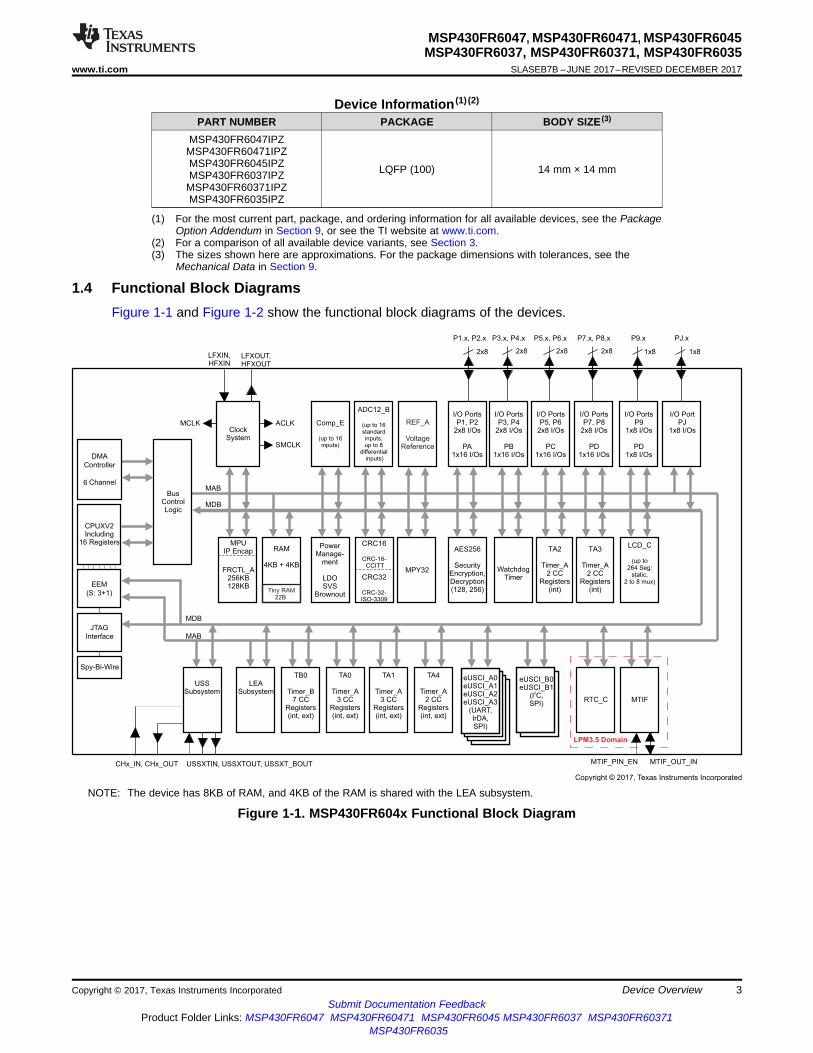
1.4 Functional Block DiagramsFigure 1-1 and Figure 1-2 show the functional block diagrams of the devices.
NOTE: The device has 8KB of RAM, and 4KB of the RAM is shared with the LEA subsystem.
Figure 1-1. MSP430FR604x Functional Block Diagram

I/O PortsP3, P4
2x8 I/Os
PB1x16 I/Os
I/O PortsP5, P6
2x8 I/Os
PC1x16 I/Os
eUSCI_A0eUSCI_A1eUSCI_A2eUSCI_A3
(UART,IrDA,SPI)
EEM
(S: 3+1)
Comp_E
(up to 16inputs)
FRCTL_A256KB128KB
RAM
4KB + 4KB
PowerMgmt
LDOSVS
Brownout
SMCLK
ACLK
LFXOUT,HFXOUT
LFXIN,HFXIN
Spy-Bi-Wire
BusControlLogic
MAB
MDB
MAB
MDB
MCLK
P1.x, P2.x
2x8
I/O PortPJ
1x8 I/Os
I/O PortsP1, P2
2x8 I/Os
PA1x16 I/Os
P3.x, P4.x PJ.x
1x2x8 8
MPY32
AES256
SecurityEncryption,Decryption(128, 256)
ADC12_B
(up to 16standardinputs,up to 8
differentialinputs)
ClockSystem
CPUXV2incl. 16
Registers
JTAG
Interface
DMA
Controller
6 Channel
Watchdog
REF_A
VoltageReference
MPUIP Encap
T 0B
Timer_B7 CC
Registers(int, ext)
TA0
Timer_A3 CC
Registers(int, ext)
TA1
Timer_A3 CC
Registers(int, ext)
T 2A
Timer_A2 CC
Registers(int)
RTC_C
eUSCI_B0eUSCI_B1
(I2C,SPI)
LPM3.5 Domain
LEA
SubSystem
I/O PortsP7, P8
2x8 I/Os
PD1x16 I/Os
P5.x, P6.x P7.x, P8.x
2x8 2x8
CRC32
CRC-32-ISO-3309
CRC16
CRC-16-CCITT
TA4
Timer_A2 CC
Registers(int, ext)
Tiny RAM22B
I/O PortsP9
1x8 I/Os
PD1x8 I/Os
P9.x
T 3A
Timer_A2 CC
Registers(int)
1x8
MTIF
LCD_C
(up to264 Seg:
static,2 to 8 mux)
MTIF_PIN_EN MTIF_OUT_IN
Copyright © 2017, Texas Instruments Incorporated
4
MSP430FR6047, MSP430FR60471, MSP430FR6045MSP430FR6037, MSP430FR60371, MSP430FR6035SLASEB7B –JUNE 2017–REVISED DECEMBER 2017 www.ti.com
Submit Documentation FeedbackProduct Folder Links: MSP430FR6047 MSP430FR60471 MSP430FR6045 MSP430FR6037 MSP430FR60371
MSP430FR6035
Device Overview Copyright © 2017, Texas Instruments Incorporated
NOTE: The device has 8KB of RAM, and 4KB of the RAM is shared with the LEA subsystem.
Figure 1-2. MSP430FR603x Functional Block Diagram
5
MSP430FR6047, MSP430FR60471, MSP430FR6045MSP430FR6037, MSP430FR60371, MSP430FR6035
www.ti.com SLASEB7B –JUNE 2017–REVISED DECEMBER 2017
Submit Documentation FeedbackProduct Folder Links: MSP430FR6047 MSP430FR60471 MSP430FR6045 MSP430FR6037 MSP430FR60371
MSP430FR6035
Table of ContentsCopyright © 2017, Texas Instruments Incorporated
Table of Contents1 Device Overview ......................................... 1
1.1 Features .............................................. 11.2 Applications........................................... 21.3 Description............................................ 21.4 Functional Block Diagrams ........................... 3
2 Revision History ......................................... 63 Device Comparison ..................................... 7
3.1 Related Products ..................................... 84 Terminal Configuration and Functions.............. 9
4.1 Pin Diagram .......................................... 94.2 Pin Attributes ........................................ 114.3 Signal Descriptions.................................. 194.4 Pin Multiplexing ..................................... 284.5 Buffer Type.......................................... 284.6 Connection of Unused Pins ......................... 28
5 Specifications ........................................... 295.1 Absolute Maximum Ratings ........................ 295.2 ESD Ratings ........................................ 295.3 Recommended Operating Conditions............... 305.4 Active Mode Supply Current Into VCC Excluding
External Current .................................... 315.5 Typical Characteristics, Active Mode Supply
Currents ............................................. 325.6 Low-Power Mode (LPM0, LPM1) Supply Currents
Into VCC Excluding External Current ................ 325.7 Low-Power Mode (LPM2, LPM3, LPM4) Supply
Currents (Into VCC) Excluding External Current .... 335.8 Low-Power Mode With LCD Supply Currents (Into
VCC) Excluding External Current .................... 355.9 Low-Power Mode (LPMx.5) Supply Currents (Into
VCC) Excluding External Current .................... 365.10 Typical Characteristics, Low-Power Mode Supply
Currents ............................................. 375.11 Typical Characteristics, Current Consumption per
Module .............................................. 385.12 Thermal Resistance Characteristics for 100-Pin
LQFP (PZ) Package ................................ 385.13 Timing and Switching Characteristics ............... 39
6 Detailed Description ................................... 726.1 Overview ............................................ 726.2 CPU ................................................. 726.3 Ultrasonic Sensing Solution (USS) Module ......... 726.4 Low-Energy Accelerator (LEA) for Signal
Processing .......................................... 736.5 Operating Modes .................................... 746.6 Interrupt Vector Table and Signatures .............. 776.7 Bootloader (BSL).................................... 806.8 JTAG Operation ..................................... 816.9 FRAM Controller A (FRCTL_A) ..................... 826.10 RAM ................................................ 826.11 Tiny RAM............................................ 826.12 Memory Protection Unit (MPU) Including IP
Encapsulation ....................................... 826.13 Peripherals .......................................... 836.14 Input/Output Diagrams .............................. 956.15 Device Descriptors (TLV) .......................... 1406.16 Memory Map ....................................... 1436.17 Identification........................................ 166
7 Applications, Implementation, and Layout ...... 1677.1 Device Connection and Layout Fundamentals .... 1677.2 Peripheral- and Interface-Specific Design
Information ......................................... 1738 Device and Documentation Support .............. 176
8.1 Getting Started and Next Steps ................... 1768.2 Device and Development Tool Nomenclature ..... 1768.3 Tools and Software ................................ 1788.4 Documentation Support............................ 1798.5 Related Links ...................................... 1808.6 Trademarks ........................................ 1808.7 Electrostatic Discharge Caution ................... 1818.8 Export Control Notice .............................. 1818.9 Glossary............................................ 181
9 Mechanical, Packaging, and OrderableInformation ............................................. 181
6
MSP430FR6047, MSP430FR60471, MSP430FR6045MSP430FR6037, MSP430FR60371, MSP430FR6035SLASEB7B –JUNE 2017–REVISED DECEMBER 2017 www.ti.com
Submit Documentation FeedbackProduct Folder Links: MSP430FR6047 MSP430FR60471 MSP430FR6045 MSP430FR6037 MSP430FR60371
MSP430FR6035
Revision History Copyright © 2017, Texas Instruments Incorporated
2 Revision History
Changes from September 26, 2017 to December 15, 2017 Page
• Changed document status to Production Data ................................................................................... 1• Added Section 3.1, Related Products ............................................................................................. 8• Updated Section 5, Specifications, with data for production silicon .......................................................... 29

Copyright © 2017, Texas Instruments Incorporated Device ComparisonSubmit Documentation Feedback
Product Folder Links: MSP430FR6047 MSP430FR60471 MSP430FR6045 MSP430FR6037 MSP430FR60371MSP430FR6035
7
MSP430FR6047, MSP430FR60471, MSP430FR6045MSP430FR6037, MSP430FR60371, MSP430FR6035
www.ti.com SLASEB7B –JUNE 2017–REVISED DECEMBER 2017
3 Device Comparison
Table 3-1 summarizes the available family members.
(1) For the most current package and ordering information, see the Package Option Addendum in Section 9, or see the TI website at www.ti.com.(2) Package drawings, standard packing quantities, thermal data, symbolization, and PCB design guidelines are available at www.ti.com/packaging.(3) Each number in the sequence represents an instantiation of Timer_A with its associated number of capture/compare registers and PWM output generators available. For example, a
number sequence of 3, 5 would represent two instantiations of Timer_A, the first instantiation having three capture/compare registers and PWM output generators and the secondinstantiation having five capture/compare registers and PWM output generators, respectively.
(4) Each number in the sequence represents an instantiation of Timer_B with its associated number of capture/compare registers and PWM output generators available. For example, anumber sequence of 3, 5 would represent two instantiations of Timer_B, the first instantiation having three capture/compare registers and PWM output generators and the secondinstantiation having five capture/compare registers and PWM output generators, respectively.
(5) eUSCI_A supports UART with automatic baud-rate detection, IrDA encode and decode, and SPI.(6) eUSCI_B supports I2C with multiple slave addresses and SPI.(7) Timers TA0 and TA1 provide internal and external capture/compare inputs and internal and external PWM outputs.(8) Timers TA2 and TA3 provide only internal capture/compare inputs and only internal PWM outputs (if any) whereas Timer TA4 provides internal, external capture/compare inputs and
internal, external PWM outputs.
Table 3-1. Device Comparison (1) (2)
DEVICE FRAM(KB)
SRAM(KB)
CLOCKSYSTEM LEA USS
USSXT MTIF ADC12_B Comp_E Timer_A (3) Timer_B (4) eUSCIAES BSL I/Os PACKAGE
A (5) B (6)
MSP430FR6047 256 8DCOHFXTLFXT
Yes Yes Yes 16 ext, 2 int ch. 16 ch. 3, 3 (7)
2, 2,2 (8) 7 4 2 Yes UART 76 100 PZ (LQFP)
MSP430FR60471 256 8DCOHFXTLFXT
Yes Yes Yes 16 ext, 2 int ch. 16 ch. 3, 3 (7)
2, 2,2 (8) 7 4 2 Yes I2C 76 100 PZ (LQFP)
MSP430FR6037 256 8DCOHFXTLFXT
Yes No Yes 16 ext, 2 int ch. 16 ch. 3, 3 (7)
2, 2,2 (8) 7 4 2 Yes UART 76 100 PZ (LQFP)
MSP430FR60371 256 8DCOHFXTLFXT
Yes No Yes 16 ext, 2 int ch. 16 ch. 3, 3 (7)
2, 2,2 (8) 7 4 2 Yes I2C 76 100 PZ (LQFP)
MSP430FR6045 128 8DCOHFXTLFXT
Yes Yes Yes 16 ext, 2 int ch. 16 ch. 3, 3 (7)
2, 2,2 (8) 7 4 2 Yes UART 76 100 PZ (LQFP)
MSP430FR6035 128 8DCOHFXTLFXT
Yes No Yes 16 ext, 2 int ch. 16 ch. 3, 3 (7)
2, 2,2 (8) 7 4 2 Yes UART 76 100 PZ (LQFP)
8
MSP430FR6047, MSP430FR60471, MSP430FR6045MSP430FR6037, MSP430FR60371, MSP430FR6035SLASEB7B –JUNE 2017–REVISED DECEMBER 2017 www.ti.com
Submit Documentation FeedbackProduct Folder Links: MSP430FR6047 MSP430FR60471 MSP430FR6045 MSP430FR6037 MSP430FR60371
MSP430FR6035
Device Comparison Copyright © 2017, Texas Instruments Incorporated
3.1 Related ProductsFor information about other devices in this family of products or related products, see the following links.Products for TI Microcontrollers TI's low-power and high-performance MCUs, with wired and wireless
connectivity options, are optimized for a broad range of applications.Products for MSP430 Ultra-Low-Power Microcontrollers One platform. One ecosystem. Endless
possibilities. Enabling the connected world with innovations in ultra-low-powermicrocontrollers with advanced peripherals for precise sensing and measurement.
MSP430FRxx FRAM Microcontrollers 16-bit microcontrollers for ultra-low-power sensing and systemmanagement in building automation, smart grid, and industrial designs.
Companion Products for MSP430FR6047 Review products that are frequently purchased or used withthis product.
Reference Designs for MSP430FR6047 The TI Designs Reference Design Library is a robust referencedesign library that spans analog, embedded processor, and connectivity. Created by TIexperts to help you jump start your system design, all TI Designs include schematic or blockdiagrams, BOMs, and design files to speed your time to market. Search and downloaddesigns at ti.com/tidesigns.

MSP430FR604xPZ
1P2.2/COUT/UCA0CLK/A14/C14
2P2.3/TA0.0/UCA0STE/A15/C15
3P1.0/UCA1CLK/TA1.0/A0/C0/VREF-/VeREF-
4P1.1/UCA1STE/TA4.0/A1/C1/VREF+/VeREF+
5AVSS2
6PJ.4/LFXIN
7PJ.5/LFXOUT
8AVSS3
9PJ.6/HFXIN
10PJ.7/HFXOUT
11AVSS4
12P1.4/TB0.4/ A2/C2UCB0STE/
13P1.5/TB0.5/ A3/C3UCB0CLK/
14P1.6/UCB0SIMO/UCB0SDA/A4/C4
15P1.7/USSTRG/UCB0SOMI/UCB0SCL/A5/C5
16P2.0/UCA0SIMO/UCA0TXD/A6/C6
17P2.1/UCA0SOMI/UCA0RXD/A7/C7
18P1.2/UCA1SIMO/UCA1TXD/A8/C8
19P1.3/UCA1SOMI/UCA1RXD/A9/C9
20TEST/SBWTCK
21RST /NMI/SBWTDIO
22PJ.0/TDO/ACLK/SRSCG1/DMAE0/C10
23PJ.1/TDI/TCLK/SMCLK/SRSCG0/TA4CLK/C11
24PJ.2/TMS/MCLK/SROSCOFF/TB0OUTH/C12
25PJ.3/TCK/RTCCLK/SRCPUOFF/TB0.6/C1326
DV
SS
1
27
DV
CC
1
28
P2.4
/TA
0C
LK
/TB
0C
LK
/TA
1C
LK
/LC
DS
32
29
P2.5
/TA
4.0
/LC
DS
31
30
P2.6
/TA
4.1
/LC
DS
30
31
P3.0
/TB
0.0
/LC
DS
29
32
P3.1
/TB
0.1
/LC
DS
28
33
P3.2
/TB
0.2
/LC
DS
27
34
P3.3
/TB
0.3
/LC
DS
26
35
P3.4
/TB
0O
UT
H/L
CD
S25
36
P3.5
/TB
0.4
/LC
DS
24
37
P3.6
/TB
0.5
/LC
DS
23
38
P3.7
/TB
0.6
/LC
DS
22
39
P2.7
/TA
0.0
/LC
DS
21
40
P9.0
/TA
1.0
/LC
DS
20
41
P9.1
/SM
CLK
/LC
DS
19
42
P9.2
/MC
LK
/LC
DS
18
43
P9.3
/AC
LK
/LC
DS
17
44
P4.0
/RT
CC
LK
/LC
DS
16
45
P4.1
/UC
A0C
LK
/LC
DS
15
46
P4.2
/UC
A0S
TE
/LC
DS
14
47
P4.3
/UC
A0S
IMO
/UC
A0T
XD
/LC
DS
13
48
P4.4
/UC
A0S
OM
I/U
CA
0R
XD
/LC
DS
12
49
P4.5
/TA
0C
LK
/TA
1C
LK
/LC
DS
11
50
P4.6
/TB
0C
LK
/TA
4C
LK
/LC
DS
10
51 DVSS2
52 DVCC2
53 P4.7/DMAE0/LCDS9
54 P5.0/UCA2SIMO/UCA2TXD/LCDS8
55 P5.1/UCA2SOMI/UCA2RXD/LCDS7
56 P5.2/UCA2CLK/LCDS6
57 P5.3/UCA2STE/LCDS5
58 P5.4/UCB1CLK/LCDS4
59 P5.5/TA0CLK/UCB1SIMO/UCB1SDA/LCDS3
60 P5.6/UCB1SOMI/UCB1SCL/LCDS2
61 P5.7/UCB1STE/LCDS1
62 P6.0/COUT/LCDS0
63 P6.4/COM0
64 P6.5/COM1
65 P6.6/COM2/LCDS38
66 P6.7/COM3/LCDS37
67 P7.0/UCA2SIMO/UCA2TXD/ACLK/COM4/LCDS36
68 P7.1/UCA2SOMI/UCA2RXD/SMCLK/COM5/LCDS35
69 P7.2/UCA2CLK/TB0.0/COM6/LCDS34
70 P7.3/UCA2STE/TB0.1/COM7/LCDS33
71 P6.1/R03
72 P6.2/R13/LCDREF
73 P6.3/R23
74 R33/LCDCAP
75 DVSS376
DV
CC
3
77
P7.4
/TA
0.1
/MT
IF_O
UT
_IN
78
P7.5
/TA
1.1
/MT
IF_P
IN_E
N
79
P8.0
/UC
A3S
TE
/TB
0.2
/DM
AE
0
80
P8.1
/UC
A3C
LK
/TB
0.3
/TB
0O
UT
H
81
P8.2
/UC
A3S
OM
I/U
CA
3R
XD
/MC
LK
82
P8.3
/UC
A3S
IMO
/UC
A3T
XD
/RT
CC
LK
83
P7.6
/TA
4.1
/DM
AE
0/C
OU
T
84
P7.7
/TA
0.2
/TB
0O
UT
H/C
OU
T
85
CH
1_IN
86
CH
1_O
UT
87
PV
SS
88
PV
CC
89
PV
SS
90
CH
0_O
UT
91
CH
0_IN
92
P8.4
/UC
B1C
LK
/TA
1.2
/A10
93
P8.5
/UC
B1S
IMO
/UC
B1S
DA
/A11
94P
8.6
/UC
B1S
OM
I/U
CB
1S
CL/A
12
95
P8.7
/UC
B1S
TE
/US
SX
T_B
OU
T/A
13
96
AV
SS
5
97
US
SX
TIN
98
US
SX
TO
UT
99
AV
SS
1
100
AV
CC
1
9
MSP430FR6047, MSP430FR60471, MSP430FR6045MSP430FR6037, MSP430FR60371, MSP430FR6035
www.ti.com SLASEB7B –JUNE 2017–REVISED DECEMBER 2017
Submit Documentation FeedbackProduct Folder Links: MSP430FR6047 MSP430FR60471 MSP430FR6045 MSP430FR6037 MSP430FR60371
MSP430FR6035
Terminal Configuration and FunctionsCopyright © 2017, Texas Instruments Incorporated
4 Terminal Configuration and Functions
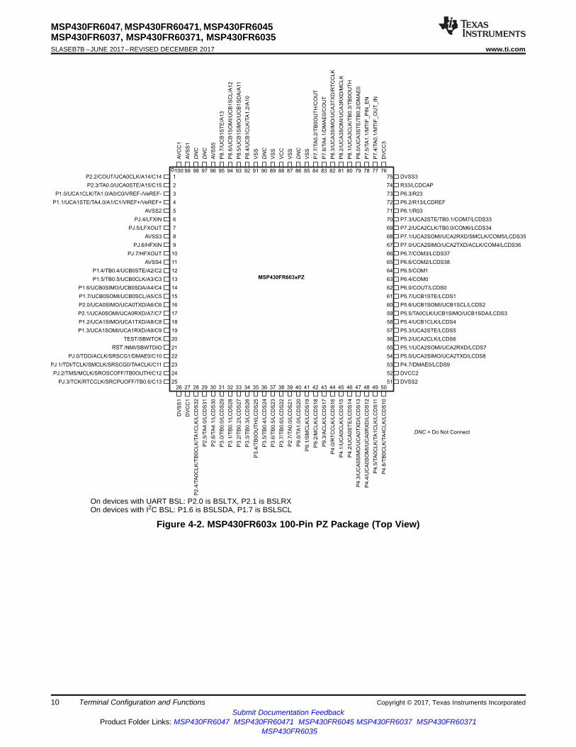
4.1 Pin DiagramFigure 4-1 and Figure 4-2 show the pinouts of the 100-pin PZ packages.
On devices with UART BSL: P2.0 is BSLTX, P2.1 is BSLRXOn devices with I2C BSL: P1.6 is BSLSDA, P1.7 is BSLSCL
Figure 4-1. MSP430FR604x 100-Pin PZ Package (Top View)
MSP430FR603xPZ
1P2.2/COUT/UCA0CLK/A14/C14
2P2.3/TA0.0/UCA0STE/A15/C15
3P1.0/UCA1CLK/TA1.0/A0/C0/VREF-/VeREF-
4P1.1/UCA1STE/TA4.0/A1/C1/VREF+/VeREF+
5AVSS2
6PJ.4/LFXIN
7PJ.5/LFXOUT
8AVSS3
9PJ.6/HFXIN
10PJ.7/HFXOUT
11AVSS4
12P1.4/TB0.4/ A2/C2UCB0STE/
13P1.5/TB0.5/ A3/C3UCB0CLK/
14P1.6/UCB0SIMO/UCB0SDA/A4/C4
15P1.7/UCB0SOMI/UCB0SCL/A5/C5
16P2.0/UCA0SIMO/UCA0TXD/A6/C6
17P2.1/UCA0SOMI/UCA0RXD/A7/C7
18P1.2/UCA1SIMO/UCA1TXD/A8/C8
19P1.3/UCA1SOMI/UCA1RXD/A9/C9
20TEST/SBWTCK
21RST /NMI/SBWTDIO
22PJ.0/TDO/ACLK/SRSCG1/DMAE0/C10
23PJ.1/TDI/TCLK/SMCLK/SRSCG0/TA4CLK/C11
24PJ.2/TMS/MCLK/SROSCOFF/TB0OUTH/C12
25PJ.3/TCK/RTCCLK/SRCPUOFF/TB0.6/C1326
DV
SS
1
27
DV
CC
1
28
P2.4
/TA
0C
LK
/TB
0C
LK
/TA
1C
LK
/LC
DS
32
29
P2.5
/TA
4.0
/LC
DS
31
30
P2.6
/TA
4.1
/LC
DS
30
31
P3.0
/TB
0.0
/LC
DS
29
32
P3.1
/TB
0.1
/LC
DS
28
33
P3.2
/TB
0.2
/LC
DS
27
34
P3.3
/TB
0.3
/LC
DS
26
35
P3.4
/TB
0O
UT
H/L
CD
S25
36
P3.5
/TB
0.4
/LC
DS
24
37
P3.6
/TB
0.5
/LC
DS
23
38
P3.7
/TB
0.6
/LC
DS
22
39
P2.7
/TA
0.0
/LC
DS
21
40
P9.0
/TA
1.0
/LC
DS
20
41
P9.1
/SM
CLK
/LC
DS
19
42
P9.2
/MC
LK
/LC
DS
18
43
P9.3
/AC
LK
/LC
DS
17
44
P4.0
/RT
CC
LK
/LC
DS
16
45
P4.1
/UC
A0C
LK
/LC
DS
15
46
P4.2
/UC
A0S
TE
/LC
DS
14
47
P4.3
/UC
A0S
IMO
/UC
A0T
XD
/LC
DS
13
48
P4.4
/UC
A0S
OM
I/U
CA
0R
XD
/LC
DS
12
49
P4.5
/TA
0C
LK
/TA
1C
LK
/LC
DS
11
50P
4.6
/TB
0C
LK
/TA
4C
LK
/LC
DS
10
51 DVSS2
52 DVCC2
53 P4.7/DMAE0/LCDS9
54 P5.0/UCA2SIMO/UCA2TXD/LCDS8
55 P5.1/UCA2SOMI/UCA2RXD/LCDS7
56 P5.2/UCA2CLK/LCDS6
57 P5.3/UCA2STE/LCDS5
58 P5.4/UCB1CLK/LCDS4
59 P5.5/TA0CLK/UCB1SIMO/UCB1SDA/LCDS3
60 P5.6/UCB1SOMI/UCB1SCL/LCDS2
61 P5.7/UCB1STE/LCDS1
62 P6.0/COUT/LCDS0
63 P6.4/COM0
64 P6.5/COM1
65 P6.6/COM2/LCDS38
66 P6.7/COM3/LCDS37
67 P7.0/UCA2SIMO/UCA2TXD/ACLK/COM4/LCDS36
68 P7.1/UCA2SOMI/UCA2RXD/SMCLK/COM5/LCDS35
69 P7.2/UCA2CLK/TB0.0/COM6/LCDS34
70 P7.3/UCA2STE/TB0.1/COM7/LCDS33
71 P6.1/R03
72 P6.2/R13/LCDREF
73 P6.3/R23
74 R33/LCDCAP
75 DVSS376
DV
CC
3
77
P7.4
/TA
0.1
/MT
IF_O
UT
_IN
78
P7.5
/TA
1.1
/MT
IF_P
IN_E
N
79
P8.0
/UC
A3S
TE
/TB
0.2
/DM
AE
0
80
P8.1
/UC
A3C
LK
/TB
0.3
/TB
0O
UT
H
81
P8.2
/UC
A3S
OM
I/U
CA
3R
XD
/MC
LK
82
P8.3
/UC
A3S
IMO
/UC
A3T
XD
/RT
CC
LK
83
P7.6
/TA
4.1
/DM
AE
0/C
OU
T
84
P7.7
/TA
0.2
/TB
0O
UT
H/C
OU
T
85
VS
S
86
DN
C
87
VS
S
88
VC
C
89
VS
S
90
DN
C
91
VS
S
92
P8.4
/UC
B1C
LK
/TA
1.2
/A10
93
P8.5
/UC
B1S
IMO
/UC
B1S
DA
/A11
94
P8.6
/UC
B1S
OM
I/U
CB
1S
CL/A
12
95
P8.7
/UC
B1S
TE
/A13
96
AV
SS
5
97
DN
C
98
DN
C
99
AV
SS
1
100
AV
CC
1
DNC = Do Not Connect
10
MSP430FR6047, MSP430FR60471, MSP430FR6045MSP430FR6037, MSP430FR60371, MSP430FR6035SLASEB7B –JUNE 2017–REVISED DECEMBER 2017 www.ti.com
Submit Documentation FeedbackProduct Folder Links: MSP430FR6047 MSP430FR60471 MSP430FR6045 MSP430FR6037 MSP430FR60371
MSP430FR6035
Terminal Configuration and Functions Copyright © 2017, Texas Instruments Incorporated
On devices with UART BSL: P2.0 is BSLTX, P2.1 is BSLRXOn devices with I2C BSL: P1.6 is BSLSDA, P1.7 is BSLSCL
Figure 4-2. MSP430FR603x 100-Pin PZ Package (Top View)

11
MSP430FR6047, MSP430FR60471, MSP430FR6045MSP430FR6037, MSP430FR60371, MSP430FR6035
www.ti.com SLASEB7B –JUNE 2017–REVISED DECEMBER 2017
Submit Documentation FeedbackProduct Folder Links: MSP430FR6047 MSP430FR60471 MSP430FR6045 MSP430FR6037 MSP430FR60371
MSP430FR6035
Terminal Configuration and FunctionsCopyright © 2017, Texas Instruments Incorporated
(1) The signal that is listed first for each pin is the reset default pin name.(2) To determine the pin mux encodings for each pin, see Section 6.14.(3) Signal Types: I = Input, O = Output, I/O = Input or Output.(4) Buffer Types: LVCMOS, Analog, or Power (see Table 4-3 for details)(5) The power source shown in this table is the I/O power source, which may differ from the module power source.(6) Reset States:
OFF = High impedance with Schmitt-trigger input and pullup or pulldown (if available) disabledPU = Pullup is enabledPD = Pulldown is enabledN/A = Not applicable
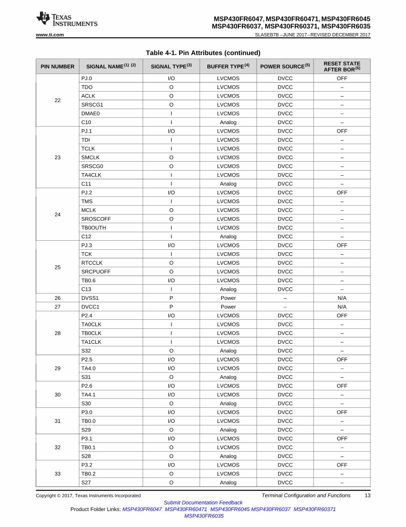
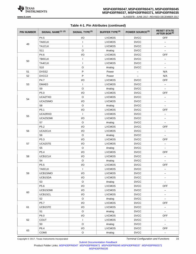
4.2 Pin AttributesTable 4-1 lists the attributes of each pin.
Table 4-1. Pin Attributes
PIN NUMBER SIGNAL NAME (1) (2) SIGNAL TYPE (3) BUFFER TYPE (4) POWER SOURCE (5) RESET STATEAFTER BOR (6)
1
P2.2 I/O LVCMOS DVCC OFFCOUT O LVCMOS DVCC –UCA0CLK I/O LVCMOS DVCC –A14 I Analog DVCC –C14 I Analog DVCC –
2
P2.3 I/O LVCMOS DVCC OFFTA0.0 I/O LVCMOS DVCC –UCA0STE I/O LVCMOS DVCC –A15 I Analog DVCC –C15 I Analog DVCC –
3
P1.0 I/O LVCMOS DVCC OFFUCA1CLK I/O LVCMOS DVCC –TA1.0 I/O LVCMOS DVCC –A0 I Analog DVCC –C0 I Analog DVCC –VREF- O Analog DVCC –VeREF- I Analog DVCC –
4
P1.1 I/O LVCMOS DVCC OFFUCA1STE I/O LVCMOS DVCC –TA4.0 I/O LVCMOS DVCC –A1 I Analog DVCC –C1 I Analog DVCC –VREF+ O Analog DVCC –VeREF+ I Analog DVCC –
5 AVSS2 P Power – N/A
6PJ.4 I/O LVCMOS DVCC OFFLFXIN I Analog DVCC –
7PJ.5 I/O LVCMOS DVCC OFFLFXOUT O Analog DVCC –
8 AVSS3 P Power – N/A
9PJ.6 I/O LVCMOS DVCC –HFXIN I Analog DVCC –
10PJ.7 I/O LVCMOS DVCC OFFHFXOUT O Analog DVCC –
11 AVSS4 P Power – N/A

12
MSP430FR6047, MSP430FR60471, MSP430FR6045MSP430FR6037, MSP430FR60371, MSP430FR6035SLASEB7B –JUNE 2017–REVISED DECEMBER 2017 www.ti.com
Submit Documentation FeedbackProduct Folder Links: MSP430FR6047 MSP430FR60471 MSP430FR6045 MSP430FR6037 MSP430FR60371
MSP430FR6035
Terminal Configuration and Functions Copyright © 2017, Texas Instruments Incorporated
Table 4-1. Pin Attributes (continued)
PIN NUMBER SIGNAL NAME (1) (2) SIGNAL TYPE (3) BUFFER TYPE (4) POWER SOURCE (5) RESET STATEAFTER BOR (6)
12
P1.4 I/O LVCMOS DVCC OFFTB0.4 I/O LVCMOS DVCC –UCB0STE I/O LVCMOS DVCC –A2 I Analog DVCC –C2 I Analog DVCC –
13
P1.5 I/O LVCMOS DVCC OFFTB0.5 I/O LVCMOS DVCC –UCB0CLK I/O LVCMOS DVCC –A3 I Analog DVCC –C3 I Analog DVCC –
14
P1.6 I/O LVCMOS DVCC OFFUCB0SIMO I/O LVCMOS DVCC –UCB0SDA I/O LVCMOS DVCC –A4 I Analog DVCC –C4 I Analog DVCC –
15
P1.7 I/O LVCMOS DVCC OFFUSSTRG I LVCMOS DVCC –UCB0SOMI I/O LVCMOS DVCC –UCB0SCL I/O LVCMOS DVCC –A5 I Analog DVCC –C5 I Analog DVCC –
16
P2.0 I/O LVCMOS DVCC OFFUCA0TXD O LVCMOS DVCC –UCA0SIMO I/O LVCMOS DVCC –A6 I Analog DVCC –C6 I Analog DVCC –
17
P2.1 I/O LVCMOS DVCC OFFUCA0RXD I LVCMOS DVCC –UCA0SOMI I/O LVCMOS DVCC –A7 I Analog DVCC –C7 I Analog DVCC –
18
P1.2 I/O LVCMOS DVCC OFFUCA1TXD O LVCMOS DVCC –UCA1SIMO I/O LVCMOS DVCC –A8 I Analog DVCC –C8 I Analog DVCC –
19
P1.3 I/O LVCMOS DVCC OFFUCA1RXD I LVCMOS DVCC –UCA1SOMI I/O LVCMOS DVCC –A9 I Analog DVCC –C9 I Analog DVCC –
20TEST I LVCMOS DVCC PDSBWTCK I LVCMOS DVCC –
21RST I/O LVCMOS DVCC PUNMI I LVCMOS DVCC –SBWTDIO I/O LVCMOS DVCC –
13
MSP430FR6047, MSP430FR60471, MSP430FR6045MSP430FR6037, MSP430FR60371, MSP430FR6035
www.ti.com SLASEB7B –JUNE 2017–REVISED DECEMBER 2017
Submit Documentation FeedbackProduct Folder Links: MSP430FR6047 MSP430FR60471 MSP430FR6045 MSP430FR6037 MSP430FR60371
MSP430FR6035
Terminal Configuration and FunctionsCopyright © 2017, Texas Instruments Incorporated
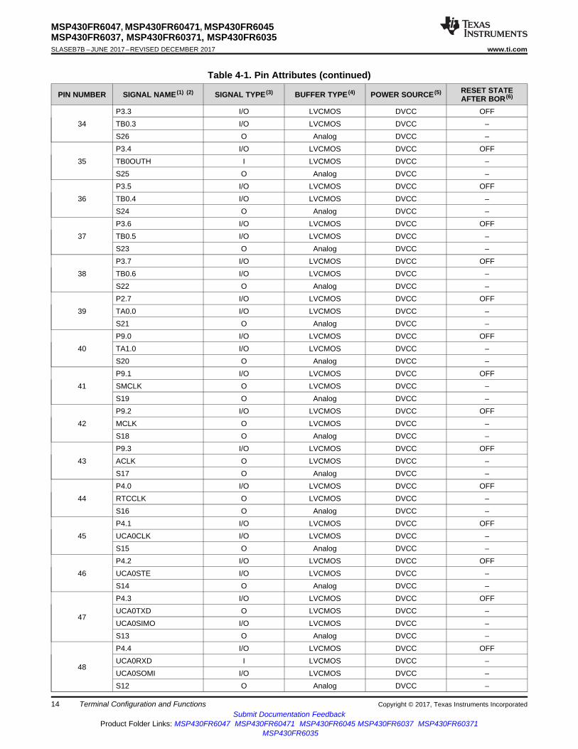
Table 4-1. Pin Attributes (continued)
PIN NUMBER SIGNAL NAME (1) (2) SIGNAL TYPE (3) BUFFER TYPE (4) POWER SOURCE (5) RESET STATEAFTER BOR (6)
22
PJ.0 I/O LVCMOS DVCC OFFTDO O LVCMOS DVCC –ACLK O LVCMOS DVCC –SRSCG1 O LVCMOS DVCC –DMAE0 I LVCMOS DVCC –C10 I Analog DVCC –
23
PJ.1 I/O LVCMOS DVCC OFFTDI I LVCMOS DVCC –TCLK I LVCMOS DVCC –SMCLK O LVCMOS DVCC –SRSCG0 O LVCMOS DVCC –TA4CLK I LVCMOS DVCC –C11 I Analog DVCC –
24
PJ.2 I/O LVCMOS DVCC OFFTMS I LVCMOS DVCC –MCLK O LVCMOS DVCC –SROSCOFF O LVCMOS DVCC –TB0OUTH I LVCMOS DVCC –C12 I Analog DVCC –
25
PJ.3 I/O LVCMOS DVCC OFFTCK I LVCMOS DVCC –RTCCLK O LVCMOS DVCC –SRCPUOFF O LVCMOS DVCC –TB0.6 I/O LVCMOS DVCC –C13 I Analog DVCC –
26 DVSS1 P Power – N/A27 DVCC1 P Power – N/A
28
P2.4 I/O LVCMOS DVCC OFFTA0CLK I LVCMOS DVCC –TB0CLK I LVCMOS DVCC –TA1CLK I LVCMOS DVCC –S32 O Analog DVCC –
29P2.5 I/O LVCMOS DVCC OFFTA4.0 I/O LVCMOS DVCC –S31 O Analog DVCC –
30P2.6 I/O LVCMOS DVCC OFFTA4.1 I/O LVCMOS DVCC –S30 O Analog DVCC –
31P3.0 I/O LVCMOS DVCC OFFTB0.0 I/O LVCMOS DVCC –S29 O Analog DVCC –
32P3.1 I/O LVCMOS DVCC OFFTB0.1 O LVCMOS DVCC –S28 O Analog DVCC –
33P3.2 I/O LVCMOS DVCC OFFTB0.2 O LVCMOS DVCC –S27 O Analog DVCC –
14
MSP430FR6047, MSP430FR60471, MSP430FR6045MSP430FR6037, MSP430FR60371, MSP430FR6035SLASEB7B –JUNE 2017–REVISED DECEMBER 2017 www.ti.com
Submit Documentation FeedbackProduct Folder Links: MSP430FR6047 MSP430FR60471 MSP430FR6045 MSP430FR6037 MSP430FR60371
MSP430FR6035
Terminal Configuration and Functions Copyright © 2017, Texas Instruments Incorporated
Table 4-1. Pin Attributes (continued)
PIN NUMBER SIGNAL NAME (1) (2) SIGNAL TYPE (3) BUFFER TYPE (4) POWER SOURCE (5) RESET STATEAFTER BOR (6)
34P3.3 I/O LVCMOS DVCC OFFTB0.3 I/O LVCMOS DVCC –S26 O Analog DVCC –
35P3.4 I/O LVCMOS DVCC OFFTB0OUTH I LVCMOS DVCC –S25 O Analog DVCC –
36P3.5 I/O LVCMOS DVCC OFFTB0.4 I/O LVCMOS DVCC –S24 O Analog DVCC –
37P3.6 I/O LVCMOS DVCC OFFTB0.5 I/O LVCMOS DVCC –S23 O Analog DVCC –
38P3.7 I/O LVCMOS DVCC OFFTB0.6 I/O LVCMOS DVCC –S22 O Analog DVCC –
39P2.7 I/O LVCMOS DVCC OFFTA0.0 I/O LVCMOS DVCC –S21 O Analog DVCC –
40P9.0 I/O LVCMOS DVCC OFFTA1.0 I/O LVCMOS DVCC –S20 O Analog DVCC –
41P9.1 I/O LVCMOS DVCC OFFSMCLK O LVCMOS DVCC –S19 O Analog DVCC –
42P9.2 I/O LVCMOS DVCC OFFMCLK O LVCMOS DVCC –S18 O Analog DVCC –
43P9.3 I/O LVCMOS DVCC OFFACLK O LVCMOS DVCC –S17 O Analog DVCC –
44P4.0 I/O LVCMOS DVCC OFFRTCCLK O LVCMOS DVCC –S16 O Analog DVCC –
45P4.1 I/O LVCMOS DVCC OFFUCA0CLK I/O LVCMOS DVCC –S15 O Analog DVCC –
46P4.2 I/O LVCMOS DVCC OFFUCA0STE I/O LVCMOS DVCC –S14 O Analog DVCC –
47
P4.3 I/O LVCMOS DVCC OFFUCA0TXD O LVCMOS DVCC –UCA0SIMO I/O LVCMOS DVCC –S13 O Analog DVCC –
48
P4.4 I/O LVCMOS DVCC OFFUCA0RXD I LVCMOS DVCC –UCA0SOMI I/O LVCMOS DVCC –S12 O Analog DVCC –
15
MSP430FR6047, MSP430FR60471, MSP430FR6045MSP430FR6037, MSP430FR60371, MSP430FR6035
www.ti.com SLASEB7B –JUNE 2017–REVISED DECEMBER 2017
Submit Documentation FeedbackProduct Folder Links: MSP430FR6047 MSP430FR60471 MSP430FR6045 MSP430FR6037 MSP430FR60371
MSP430FR6035
Terminal Configuration and FunctionsCopyright © 2017, Texas Instruments Incorporated
Table 4-1. Pin Attributes (continued)
PIN NUMBER SIGNAL NAME (1) (2) SIGNAL TYPE (3) BUFFER TYPE (4) POWER SOURCE (5) RESET STATEAFTER BOR (6)
49
P4.5 I/O LVCMOS DVCC OFFTA0CLK I LVCMOS DVCC –TA1CLK I LVCMOS DVCC –S11 O Analog DVCC –
50
P4.6 I/O LVCMOS DVCC OFFTB0CLK I LVCMOS DVCC –TA4CLK I LVCMOS DVCC –S10 O Analog DVCC –
51 DVSS2 P Power – N/A52 DVCC2 P Power – N/A
53P4.7 I/O LVCMOS DVCC OFFDMAE0 I LVCMOS DVCC –S9 O Analog DVCC –
54
P5.0 I/O LVCMOS DVCC OFFUCA2TXD O LVCMOS DVCC –UCA2SIMO I/O LVCMOS DVCC –S8 O Analog DVCC –
55
P5.1 I/O LVCMOS DVCC OFFUCA2RXD I LVCMOS DVCC –UCA2SOMI I/O LVCMOS DVCC –S7 O Analog DVCC –
56P5.2 I/O LVCMOS DVCC OFFUCA2CLK I/O LVCMOS DVCC –S6 O Analog DVCC –
57P5.3 I/O LVCMOS DVCC OFFUCA2STE I/O LVCMOS DVCC –S5 O Analog DVCC –
58P5.4 I/O LVCMOS DVCC OFFUCB1CLK I/O LVCMOS DVCC –S4 O Analog DVCC –
59
P5.5 I/O LVCMOS DVCC OFFTA0CLK I LVCMOS DVCC –UCB1SIMO I/O LVCMOS DVCC –UCB1SDA I/O LVCMOS DVCC –S3 O Analog DVCC –
60
P5.6 I/O LVCMOS DVCC OFFUCB1SOMI I/O LVCMOS DVCC –UCB1SCL I/O LVCMOS DVCC –S2 O Analog DVCC –
61P5.7 I/O LVCMOS DVCC OFFUCB1STE I/O LVCMOS DVCC –S1 O Analog DVCC –
62P6.0 I/O LVCMOS DVCC OFFCOUT I LVCMOS DVCC –S0 O Analog DVCC –
63P6.4 I/O LVCMOS DVCC OFFCOM0 O Analog DVCC –

16
MSP430FR6047, MSP430FR60471, MSP430FR6045MSP430FR6037, MSP430FR60371, MSP430FR6035SLASEB7B –JUNE 2017–REVISED DECEMBER 2017 www.ti.com
Submit Documentation FeedbackProduct Folder Links: MSP430FR6047 MSP430FR60471 MSP430FR6045 MSP430FR6037 MSP430FR60371
MSP430FR6035
Terminal Configuration and Functions Copyright © 2017, Texas Instruments Incorporated
Table 4-1. Pin Attributes (continued)
PIN NUMBER SIGNAL NAME (1) (2) SIGNAL TYPE (3) BUFFER TYPE (4) POWER SOURCE (5) RESET STATEAFTER BOR (6)
64P6.5 I/O LVCMOS DVCC OFFCOM1 O Analog DVCC –
65P6.6 I/O LVCMOS DVCC OFFCOM2 O Analog DVCC –S38 O Analog DVCC –
66P6.7 I/O LVCMOS DVCC OFFCOM3 O Analog DVCC –S37 O Analog DVCC –
67
P7.0 I/O LVCMOS DVCC OFFUCA2TXD O LVCMOS DVCC –UCA2SIMO I/O LVCMOS DVCC –ACLK O LVCMOS DVCC –COM4 O Analog DVCC –S36 O Analog DVCC –
68
P7.1 I/O LVCMOS DVCC OFFUCA2RXD I LVCMOS DVCC –UCA2SOMI I/O LVCMOS DVCC –SMCLK O LVCMOS DVCC –COM5 O Analog DVCC –S35 O Analog DVCC –
69
P7.2 I/O LVCMOS DVCC OFFUCA2CLK I/O LVCMOS DVCC –TB0.0 I/O LVCMOS DVCC –COM6 O Analog DVCC –S34 O Analog DVCC –
70
P7.3 I/O LVCMOS DVCC OFFUCA2STE I/O LVCMOS DVCC –TB0.1 I/O LVCMOS DVCC –COM7 O Analog DVCC –S33 O Analog DVCC –
71P6.1 I/O LVCMOS DVCC OFFR03 I/O Analog DVCC –
72P6.2 I/O LVCMOS DVCC OFFR13 I/O Analog DVCC –LCDREF I Analog - –
73P6.3 I/O LVCMOS DVCC OFFR23 I/O Analog DVCC –
74R33 I/O Analog DVCC -LCDCAP I/O Analog DVCC –
75 DVSS3 P Power – N/A76 DVCC3 P Power – N/A
77P7.4 I/O LVCMOS DVCC OFFTA0.1 I/O LVCMOS DVCC –MTIF_OUT_IN I/O LVCMOS DVCC –
78P7.5 I/O LVCMOS DVCC OFFTA1.1 I/O LVCMOS DVCC –MTIF_PIN_EN I LVCMOS DVCC –

17
MSP430FR6047, MSP430FR60471, MSP430FR6045MSP430FR6037, MSP430FR60371, MSP430FR6035
www.ti.com SLASEB7B –JUNE 2017–REVISED DECEMBER 2017
Submit Documentation FeedbackProduct Folder Links: MSP430FR6047 MSP430FR60471 MSP430FR6045 MSP430FR6037 MSP430FR60371
MSP430FR6035
Terminal Configuration and FunctionsCopyright © 2017, Texas Instruments Incorporated
Table 4-1. Pin Attributes (continued)
PIN NUMBER SIGNAL NAME (1) (2) SIGNAL TYPE (3) BUFFER TYPE (4) POWER SOURCE (5) RESET STATEAFTER BOR (6)
79
P8.0 I/O LVCMOS DVCC OFFUCA3STE I/O LVCMOS DVCC –TB0.2 I/O LVCMOS DVCC –DMAE0 I LVCMOS DVCC –
80
P8.1 I/O LVCMOS DVCC OFFUCA3CLK I/O LVCMOS DVCC –TB0.3 I/O LVCMOS DVCC –TB0OUTH I LVCMOS DVCC –
81
P8.2 I/O LVCMOS DVCC OFFUCA3RXD O LVCMOS DVCC –UCA3SOMI I/O LVCMOS DVCC –MCLK O LVCMOS DVCC –
82
P8.3 I/O LVCMOS DVCC OFFUCA3TXD O LVCMOS DVCC –UCA3SIMO I/O LVCMOS DVCC –RTCCLK O LVCMOS DVCC –
83
P7.6 I/O LVCMOS DVCC OFFTA4.1 I/O LVCMOS DVCC –DMAE0 I LVCMOS DVCC –COUT O LVCMOS DVCC –
84
P7.7 I/O LVCMOS DVCC OFFTA0.2 I/O LVCMOS DVCC –TB0OUTH I LVCMOS DVCC –COUT O LVCMOS DVCC –
85 CH1_IN I Analog PVCC –86 CH1_OUT O Analog PVCC –87 PVSS P Power – N/A88 PVCC P Power – N/A89 PVSS P Power – N/A90 CH0_OUT O Analog PVCC –91 CH0_IN I Analog PVCC –
92
P8.4 I/O LVCMOS DVCC OFFUCB1CLK I/O LVCMOS DVCC –TA1.2 I/O LVCMOS DVCC –A10 I Analog DVCC –
93
P8.5 I/O LVCMOS DVCC OFFUCB1SIMO I/O LVCMOS DVCC –UCB1SDA I/O LVCMOS DVCC –A11 I Analog DVCC –
94
P8.6 I/O LVCMOS DVCC OFFUCB1SOMI I/O LVCMOS DVCC –UCB1SCL I/O LVCMOS DVCC –A12 I Analog DVCC –
95
P8.7 I/O LVCMOS DVCC OFFUCB1STE I/O LVCMOS DVCC –USSXT_BOUT I/O LVCMOS DVCC –A13 I Analog DVCC –

18
MSP430FR6047, MSP430FR60471, MSP430FR6045MSP430FR6037, MSP430FR60371, MSP430FR6035SLASEB7B –JUNE 2017–REVISED DECEMBER 2017 www.ti.com
Submit Documentation FeedbackProduct Folder Links: MSP430FR6047 MSP430FR60471 MSP430FR6045 MSP430FR6037 MSP430FR60371
MSP430FR6035
Terminal Configuration and Functions Copyright © 2017, Texas Instruments Incorporated
Table 4-1. Pin Attributes (continued)
PIN NUMBER SIGNAL NAME (1) (2) SIGNAL TYPE (3) BUFFER TYPE (4) POWER SOURCE (5) RESET STATEAFTER BOR (6)
(7) Do not connect USSXTIN and USSXTOUT pins to AVCC nor to DVCC. USSXTIN does not support bypass mode, so do not drive anexternal clock on the USSXTIN pin.
96 AVSS5 P Power – N/A97 USSXTIN (7) I Analog 1.5V –98 USSXTOUT (7) O Analog 1.5V –99 AVSS1 P Power – N/A
100 AVCC1 P Power – N/A

19
MSP430FR6047, MSP430FR60471, MSP430FR6045MSP430FR6037, MSP430FR60371, MSP430FR6035
www.ti.com SLASEB7B –JUNE 2017–REVISED DECEMBER 2017
Submit Documentation FeedbackProduct Folder Links: MSP430FR6047 MSP430FR60471 MSP430FR6045 MSP430FR6037 MSP430FR60371
MSP430FR6035
Terminal Configuration and FunctionsCopyright © 2017, Texas Instruments Incorporated
(1) I = input, O = output, P = power
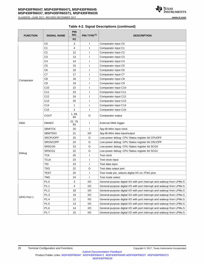
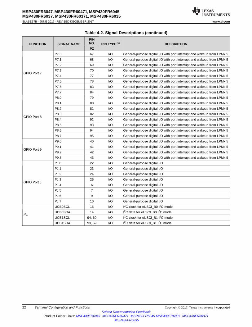
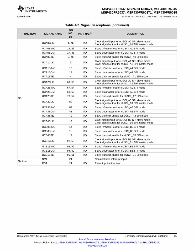
4.3 Signal DescriptionsTable 4-2 describes the signals.
Table 4-2. Signal Descriptions
FUNCTION SIGNAL NAMEPINNO. PIN TYPE (1) DESCRIPTIONPZ
ADC
A0 3 I ADC analog input A0A1 4 I ADC analog input A1A2 12 I ADC analog input A2A3 13 I ADC analog input A3A4 14 I ADC analog input A4A5 15 I ADC analog input A5A6 16 I ADC analog input A6A7 17 I ADC analog input A7A8 18 I ADC analog input A8A9 19 I ADC analog input A9A10 92 I ADC analog input A10A11 93 I ADC analog input A11A12 94 I ADC analog input A12A13 95 I ADC analog input A13A14 1 I ADC analog input A14A15 2 I ADC analog input A15VREF+ 4 O Output of positive reference voltageVREF- 3 O Output of negative reference voltageVeREF+ 4 I Input for an external positive reference voltage to the ADCVeREF- 3 I Input for an external negative reference voltage to the ADC
Clock
ACLK 22, 43,67 O ACLK output
HFXIN 9 I Input for high-frequency crystal oscillator HFXTHFXOUT 10 O Output for high-frequency crystal oscillator HFXTLFXIN 6 I Input for low-frequency crystal oscillator LFXTLFXOUT 7 O Output of low-frequency crystal oscillator LFXT
MCLK 24, 42,81 O MCLK output
SMCLK 23, 41,68 O SMCLK output
20
MSP430FR6047, MSP430FR60471, MSP430FR6045MSP430FR6037, MSP430FR60371, MSP430FR6035SLASEB7B –JUNE 2017–REVISED DECEMBER 2017 www.ti.com
Submit Documentation FeedbackProduct Folder Links: MSP430FR6047 MSP430FR60471 MSP430FR6045 MSP430FR6037 MSP430FR60371
MSP430FR6035
Terminal Configuration and Functions Copyright © 2017, Texas Instruments Incorporated
Table 4-2. Signal Descriptions (continued)
FUNCTION SIGNAL NAMEPINNO. PIN TYPE (1) DESCRIPTIONPZ
Comparator
C0 3 I Comparator input C0C1 4 I Comparator input C1C2 12 I Comparator input C2C3 13 I Comparator input C3C4 14 I Comparator input C4C5 15 I Comparator input C5C6 16 I Comparator input C6C7 17 I Comparator input C7C8 18 I Comparator input C8C9 19 I Comparator input C9C10 22 I Comparator input C10C11 23 I Comparator input C11C12 24 I Comparator input C12C13 25 I Comparator input C13C14 1 I Comparator input C14C15 2 I Comparator input C15
COUT 1, 83,84 O Comparator output
DMA DMAE0 22, 79,83 I External DMA trigger
Debug
SBWTCK 20 I Spy-Bi-Wire input clockSBWTDIO 21 I/O Spy-Bi-Wire data input/outputSRCPUOFF 25 O Low-power debug: CPU Status register bit CPUOFFSROSCOFF 24 O Low-power debug: CPU Status register bit OSCOFFSRSCG0 23 O Low-power debug: CPU Status register bit SCG0SRSCG1 22 O Low-power debug: CPU Status register bit SCG1TCK 25 I Test clockTCLK 23 I Test clock inputTDI 23 I Test data inputTDO 22 O Test data output portTEST 20 I Test mode pin, selects digital I/O on JTAG pinsTMS 24 I Test mode select
GPIO Port 1
P1.0 3 I/O General-purpose digital I/O with port interrupt and wakeup from LPMx.5P1.1 4 I/O General-purpose digital I/O with port interrupt and wakeup from LPMx.5P1.2 18 I/O General-purpose digital I/O with port interrupt and wakeup from LPMx.5P1.3 19 I/O General-purpose digital I/O with port interrupt and wakeup from LPMx.5P1.4 12 I/O General-purpose digital I/O with port interrupt and wakeup from LPMx.5P1.5 13 I/O General-purpose digital I/O with port interrupt and wakeup from LPMx.5P1.6 14 I/O General-purpose digital I/O with port interrupt and wakeup from LPMx.5P1.7 15 I/O General-purpose digital I/O with port interrupt and wakeup from LPMx.5

21
MSP430FR6047, MSP430FR60471, MSP430FR6045MSP430FR6037, MSP430FR60371, MSP430FR6035
www.ti.com SLASEB7B –JUNE 2017–REVISED DECEMBER 2017
Submit Documentation FeedbackProduct Folder Links: MSP430FR6047 MSP430FR60471 MSP430FR6045 MSP430FR6037 MSP430FR60371
MSP430FR6035
Terminal Configuration and FunctionsCopyright © 2017, Texas Instruments Incorporated
Table 4-2. Signal Descriptions (continued)
FUNCTION SIGNAL NAMEPINNO. PIN TYPE (1) DESCRIPTIONPZ
GPIO Port 2
P2.0 16 I/O General-purpose digital I/O with port interrupt and wakeup from LPMx.5P2.1 17 I/O General-purpose digital I/O with port interrupt and wakeup from LPMx.5P2.2 1 I/O General-purpose digital I/O with port interrupt and wakeup from LPMx.5P2.3 2 I/O General-purpose digital I/O with port interrupt and wakeup from LPMx.5P2.4 28 I/O General-purpose digital I/O with port interrupt and wakeup from LPMx.5P2.5 29 I/O General-purpose digital I/O with port interrupt and wakeup from LPMx.5P2.6 30 I/O General-purpose digital I/O with port interrupt and wakeup from LPMx.5P2.7 39 I/O General-purpose digital I/O with port interrupt and wakeup from LPMx.5
GPIO Port 3
P3.0 31 I/O General-purpose digital I/O with port interrupt and wakeup from LPMx.5P3.1 32 I/O General-purpose digital I/O with port interrupt and wakeup from LPMx.5P3.2 33 I/O General-purpose digital I/O with port interrupt and wakeup from LPMx.5P3.3 34 I/O General-purpose digital I/O with port interrupt and wakeup from LPMx.5P3.4 35 I/O General-purpose digital I/O with port interrupt and wakeup from LPMx.5P3.5 36 I/O General-purpose digital I/O with port interrupt and wakeup from LPMx.5P3.6 37 I/O General-purpose digital I/O with port interrupt and wakeup from LPMx.5P3.7 38 I/O General-purpose digital I/O with port interrupt and wakeup from LPMx.5
GPIO Port 4
P4.0 44 I/O General-purpose digital I/O with port interrupt and wakeup from LPMx.5P4.1 45 I/O General-purpose digital I/O with port interrupt and wakeup from LPMx.5P4.2 46 I/O General-purpose digital I/O with port interrupt and wakeup from LPMx.5P4.3 47 I/O General-purpose digital I/O with port interrupt and wakeup from LPMx.5P4.4 48 I/O General-purpose digital I/O with port interrupt and wakeup from LPMx.5P4.5 49 I/O General-purpose digital I/O with port interrupt and wakeup from LPMx.5P4.6 50 I/O General-purpose digital I/O with port interrupt and wakeup from LPMx.5P4.7 53 I/O General-purpose digital I/O with port interrupt and wakeup from LPMx.5
GPIO Port 5
P5.0 54 I/O General-purpose digital I/O with port interrupt and wakeup from LPMx.5P5.1 55 I/O General-purpose digital I/O with port interrupt and wakeup from LPMx.5P5.2 56 I/O General-purpose digital I/O with port interrupt and wakeup from LPMx.5P5.3 57 I/O General-purpose digital I/O with port interrupt and wakeup from LPMx.5P5.4 58 I/O General-purpose digital I/O with port interrupt and wakeup from LPMx.5P5.5 59 I/O General-purpose digital I/O with port interrupt and wakeup from LPMx.5P5.6 60 I/O General-purpose digital I/O with port interrupt and wakeup from LPMx.5P5.7 61 I/O General-purpose digital I/O with port interrupt and wakeup from LPMx.5
GPIO Port 6
P6.0 62 I/O General-purpose digital I/O with port interrupt and wakeup from LPMx.5P6.1 71 I/O General-purpose digital I/O with port interrupt and wakeup from LPMx.5P6.2 72 I/O General-purpose digital I/O with port interrupt and wakeup from LPMx.5P6.3 73 I/O General-purpose digital I/O with port interrupt and wakeup from LPMx.5P6.4 63 I/O General-purpose digital I/O with port interrupt and wakeup from LPMx.5P6.5 64 I/O General-purpose digital I/O with port interrupt and wakeup from LPMx.5P6.6 65 I/O General-purpose digital I/O with port interrupt and wakeup from LPMx.5P6.7 66 I/O General-purpose digital I/O with port interrupt and wakeup from LPMx.5
22
MSP430FR6047, MSP430FR60471, MSP430FR6045MSP430FR6037, MSP430FR60371, MSP430FR6035SLASEB7B –JUNE 2017–REVISED DECEMBER 2017 www.ti.com
Submit Documentation FeedbackProduct Folder Links: MSP430FR6047 MSP430FR60471 MSP430FR6045 MSP430FR6037 MSP430FR60371
MSP430FR6035
Terminal Configuration and Functions Copyright © 2017, Texas Instruments Incorporated
Table 4-2. Signal Descriptions (continued)
FUNCTION SIGNAL NAMEPINNO. PIN TYPE (1) DESCRIPTIONPZ
GPIO Port 7
P7.0 67 I/O General-purpose digital I/O with port interrupt and wakeup from LPMx.5P7.1 68 I/O General-purpose digital I/O with port interrupt and wakeup from LPMx.5P7.2 69 I/O General-purpose digital I/O with port interrupt and wakeup from LPMx.5P7.3 70 I/O General-purpose digital I/O with port interrupt and wakeup from LPMx.5P7.4 77 I/O General-purpose digital I/O with port interrupt and wakeup from LPMx.5P7.5 78 I/O General-purpose digital I/O with port interrupt and wakeup from LPMx.5P7.6 83 I/O General-purpose digital I/O with port interrupt and wakeup from LPMx.5P7.7 84 I/O General-purpose digital I/O with port interrupt and wakeup from LPMx.5
GPIO Port 8
P8.0 79 I/O General-purpose digital I/O with port interrupt and wakeup from LPMx.5P8.1 80 I/O General-purpose digital I/O with port interrupt and wakeup from LPMx.5P8.2 81 I/O General-purpose digital I/O with port interrupt and wakeup from LPMx.5P8.3 82 I/O General-purpose digital I/O with port interrupt and wakeup from LPMx.5P8.4 92 I/O General-purpose digital I/O with port interrupt and wakeup from LPMx.5P8.5 93 I/O General-purpose digital I/O with port interrupt and wakeup from LPMx.5P8.6 94 I/O General-purpose digital I/O with port interrupt and wakeup from LPMx.5P8.7 95 I/O General-purpose digital I/O with port interrupt and wakeup from LPMx.5
GPIO Port 9
P9.0 40 I/O General-purpose digital I/O with port interrupt and wakeup from LPMx.5P9.1 41 I/O General-purpose digital I/O with port interrupt and wakeup from LPMx.5P9.2 42 I/O General-purpose digital I/O with port interrupt and wakeup from LPMx.5P9.3 43 I/O General-purpose digital I/O with port interrupt and wakeup from LPMx.5
GPIO Port J
PJ.0 22 I/O General-purpose digital I/OPJ.1 23 I/O General-purpose digital I/OPJ.2 24 I/O General-purpose digital I/OPJ.3 25 I/O General-purpose digital I/OPJ.4 6 I/O General-purpose digital I/OPJ.5 7 I/O General-purpose digital I/OPJ.6 9 I/O General-purpose digital I/OPJ.7 10 I/O General-purpose digital I/O
I2C
UCB0SCL 15 I/O I2C clock for eUSCI_B0 I2C modeUCB0SDA 14 I/O I2C data for eUSCI_B0 I2C modeUCB1SCL 94, 60 I/O I2C clock for eUSCI_B1 I2C modeUCB1SDA 93, 59 I/O I2C data for eUSCI_B1 I2C mode

23
MSP430FR6047, MSP430FR60471, MSP430FR6045MSP430FR6037, MSP430FR60371, MSP430FR6035
www.ti.com SLASEB7B –JUNE 2017–REVISED DECEMBER 2017
Submit Documentation FeedbackProduct Folder Links: MSP430FR6047 MSP430FR60471 MSP430FR6045 MSP430FR6037 MSP430FR60371
MSP430FR6035
Terminal Configuration and FunctionsCopyright © 2017, Texas Instruments Incorporated
Table 4-2. Signal Descriptions (continued)
FUNCTION SIGNAL NAMEPINNO. PIN TYPE (1) DESCRIPTIONPZ
LCD
COM0 63 O LCD common output COM0 for LCD backplaneCOM1 64 O LCD common output COM1 for LCD backplaneCOM2 65 O LCD common output COM2 for LCD backplaneCOM3 66 O LCD common output COM3 for LCD backplaneCOM4 67 O LCD common output COM4 for LCD backplaneCOM5 68 O LCD common output COM5 for LCD backplaneCOM6 69 O LCD common output COM6 for LCD backplaneCOM7 70 O LCD common output COM7 for LCD backplane
LCDCAP 74 I/O LCD capacitor connectionCAUTION: LCDCAP/R33 must be connected to DVSS if not used.
LCDREF 72 I External reference voltage input for regulated LCD voltageR03 71 I/O Input/output port of lowest analog LCD voltage (V5)R13 72 I/O Input/output port of third most positive analog LCD voltage (V3 or V4)R23 73 I/O Input/output port of second most positive analog LCD voltage (V2)
R33 74 I/O Input/output port of most positive analog LCD voltage (V1)CAUTION: LCDCAP/R33 must be connected to DVSS if not used.
S0 62 O LCD segment outputS1 61 O LCD segment outputS2 60 O LCD segment outputS3 59 O LCD segment outputS4 58 O LCD segment outputS5 57 O LCD segment outputS6 56 O LCD segment outputS7 55 O LCD segment outputS8 54 O LCD segment outputS9 53 O LCD segment outputS10 50 O LCD segment outputS11 49 O LCD segment outputS12 48 O LCD segment outputS13 47 O LCD segment outputS14 46 O LCD segment outputS15 45 O LCD segment outputS16 44 O LCD segment outputS17 43 O LCD segment outputS18 42 O LCD segment outputS19 41 O LCD segment outputS20 40 O LCD segment outputS21 39 O LCD segment outputS22 38 O LCD segment outputS23 37 O LCD segment outputS24 36 O LCD segment outputS25 35 O LCD segment outputS26 34 O LCD segment outputS27 33 O LCD segment outputS28 32 O LCD segment outputS29 31 O LCD segment output

24
MSP430FR6047, MSP430FR60471, MSP430FR6045MSP430FR6037, MSP430FR60371, MSP430FR6035SLASEB7B –JUNE 2017–REVISED DECEMBER 2017 www.ti.com
Submit Documentation FeedbackProduct Folder Links: MSP430FR6047 MSP430FR60471 MSP430FR6045 MSP430FR6037 MSP430FR60371
MSP430FR6035
Terminal Configuration and Functions Copyright © 2017, Texas Instruments Incorporated
Table 4-2. Signal Descriptions (continued)
FUNCTION SIGNAL NAMEPINNO. PIN TYPE (1) DESCRIPTIONPZ
LCD (continued)
S30 30 O LCD segment outputS31 29 O LCD segment outputS32 28 O LCD segment outputS33 70 O LCD segment outputS34 69 O LCD segment outputS35 68 O LCD segment outputS36 67 O LCD segment outputS37 66 O LCD segment outputS38 65 O LCD segment output
MTIFMTIF_PIN_EN 78 I Meter test interface pin enableMTIF_OUT_IN 77 I/O Meter test interface input and output
Power
AVCC1 100 P Analog power supplyAVSS1 99 P Analog ground supplyAVSS2 5 P Analog ground supplyAVSS3 8 P Analog ground supplyAVSS4 11 P Analog ground supplyAVSS5 96 P Analog ground supplyDVCC1 27 P Digital power supplyDVCC2 52 P Digital power supplyDVCC3 76 P Digital power supplyDVSS1 26 P Digital ground supplyDVSS2 51 P Digital ground supplyDVSS3 75 P Digital ground supplyPVCC 88 P USS power supplyPVSS 87, 89 P USS ground supply
RTC RTCCLK 25, 44,82 O RTC clock calibration output
25
MSP430FR6047, MSP430FR60471, MSP430FR6045MSP430FR6037, MSP430FR60371, MSP430FR6035
www.ti.com SLASEB7B –JUNE 2017–REVISED DECEMBER 2017
Submit Documentation FeedbackProduct Folder Links: MSP430FR6047 MSP430FR60471 MSP430FR6045 MSP430FR6037 MSP430FR60371
MSP430FR6035
Terminal Configuration and FunctionsCopyright © 2017, Texas Instruments Incorporated
Table 4-2. Signal Descriptions (continued)
FUNCTION SIGNAL NAMEPINNO. PIN TYPE (1) DESCRIPTIONPZ
SPI
UCA0CLK 1, 45 I/O Clock signal input for eUSCI_A0 SPI slave modeClock signal output for eUSCI_A0 SPI master mode
UCA0SIMO 16, 47 I/O Slave in/master out for eUSCI_A0 SPI modeUCA0SOMI 17, 48 I/O Slave out/master in for eUSCI_A0 SPI modeUCA0STE 2, 46 I/O Slave transmit enable for eUSCI_A0 SPI mode
UCA1CLK 3 I/O Clock signal input for eUSCI_A1 SPI slave modeClock signal output for eUSCI_A1 SPI master mode
UCA1SIMO 18 I/O Slave in/master out for eUSCI_A1 SPI modeUCA1SOMI 19 I/O Slave out/master in for eUSCI_A1 SPI modeUCA1STE 4 I/O Slave transmit enable for eUSCI_A1 SPI mode
UCA2CLK 69, 56 I/O Clock signal input for eUSCI_A2 SPI slave modeClock signal output for eUSCI_A2 SPI master mode
UCA2SIMO 67, 54 I/O Slave in/master out for eUSCI_A2 SPI modeUCA2SOMI 68, 55 I/O Slave out/master in for eUSCI_A2 SPI modeUCA2STE 70, 57 I/O Slave transmit enable for eUSCI_A2 SPI mode
UCA3CLK 80 I/O Clock signal input for eUSCI_A3 SPI slave modeClock signal output for eUSCI_A3 SPI master mode
UCA3SIMO 82 I/O Slave in/master out for eUSCI_A3 SPI modeUCA3SOMI 81 I/O Slave out/master in for eUSCI_A3 SPI modeUCA3STE 79 I/O Slave transmit enable for eUSCI_A3 SPI mode
UCB0CLK 13 I/O Clock signal input for eUSCI_B0 SPI slave modeClock signal output for eUSCI_B0 SPI master mode
UCB0SIMO 14 I/O Slave in/master out for eUSCI_B0 SPI modeUCB0SOMI 15 I/O Slave out/master in for eUSCI_B0 SPI modeUCB0STE 12 I/O Slave transmit enable for eUSCI_B0 SPI mode
UCB1CLK 92, 58 I/O Clock signal input for eUSCI_B1 SPI slave modeClock signal output for eUSCI_B1 SPI master mode
UCB1SIMO 93, 59 I/O Slave in/master out for eUSCI_B1 SPI modeUCB1SOMI 94, 60 I/O Slave out/master in for eUSCI_B1 SPI modeUCB1STE 95, 61 I/O Slave transmit enable for eUSCI_B1 SPI mode
SystemNMI 21 I Nonmaskable interrupt inputRST 21 I/O Reset input active low

26
MSP430FR6047, MSP430FR60471, MSP430FR6045MSP430FR6037, MSP430FR60371, MSP430FR6035SLASEB7B –JUNE 2017–REVISED DECEMBER 2017 www.ti.com
Submit Documentation FeedbackProduct Folder Links: MSP430FR6047 MSP430FR60471 MSP430FR6045 MSP430FR6037 MSP430FR60371
MSP430FR6035
Terminal Configuration and Functions Copyright © 2017, Texas Instruments Incorporated
Table 4-2. Signal Descriptions (continued)
FUNCTION SIGNAL NAMEPINNO. PIN TYPE (1) DESCRIPTIONPZ
Timer
TA0.0 2 I/O TA0 CCR0 capture: CCI0A input, compare: Out0TA0.0 39 I/O TA0 CCR0 capture: CCI0B input, compare: Out0TA0.1 77 I/O TA0 CCR1 capture: CCI1A input, compare: Out1TA0.2 84 I/O TA0 CCR2 capture: CCI2A input, compare: Out2
TA0CLK 28, 49,59 I TA0 input clock
TA1.0 3 I/O TA1 CCR0 capture: CCI0A input, compare: Out0TA1.0 40 I/O TA1 CCR0 capture: CCI0B input, compare: Out0TA1.1 78 I/O TA1 CCR1 capture: CCI1A input, compare: Out1TA1.2 92 I/O TA1 CCR2 capture: CCI2A input, compare: Out2TA1CLK 28, 49 I TA1 input clockTA4.0 4 I/O TA4 CCR0 capture: CCI0A input, compare: Out0TA4.0 29 I/O TA4 CCR0 capture: CCI0B input, compare: Out0TA4.1 30 I/O TA4CCR1 capture: CCI1B input, compare: Out1TA4.1 83 I/O TA4 CCR1 capture: CCI1A input, compare: Out1TA4CLK 23, 50 I TA4 input clockTB0.0 31 I/O TB0 CCR0 capture: CCI0B input, compare: Out0TB0.0 69 I/O TB0 CCR0 capture: CCI0A input, compare: Out0TB0.1 32 I/O TB0 CCR1 capture: CCI1A input, compare: Out1TB0.1 70 O TB0 CCR1 compare: Out1TB0.2 33 I/O TB0 CCR2 capture: CCI2A input, compare: Out2TB0.2 79 O TB0 CCR2 compare: Out2TB0.3 34 I/O TB0 CCR3 capture: CCI3A input, compare: Out3TB0.3 80 I/O TB0 CCR3 capture: CCI3B input, compare: Out3TB0.4 12 I/O TB0 CCR4 capture: CCI4A input, compare: Out4TB0.4 36 I/O TB0 CCR4 capture: CCI4B input, compare: Out4TB0.5 13 I/O TB0 CCR5 capture: CCI5A input, compare: Out5TB0.5 37 I/O TB0CCR5 capture: CCI5B input, compare: Out5TB0.6 25 I/O TB0 CCR6 capture: CCI6B input, compare: Out6TB0.6 38 I/O TB0 CCR6 capture: CCI6A input, compare: Out6TB0CLK 28, 50 I TB0 clock input
TB0OUTH 24, 35,80, 84 I Switch all PWM outputs high impedance input – TB0
UART
UCA0RXD 17, 48 I Receive data for eUSCI_A0 UART modeUCA0TXD 16, 47 O Transmit data for eUSCI_A0 UART modeUCA1RXD 19 I Receive data for eUSCI_A1 UART modeUCA1TXD 18 O Transmit data for eUSCI_A1 UART modeUCA2RXD 68, 55 I Receive data for eUSCI_A2 UART modeUCA2TXD 67, 54 O Transmit data for eUSCI_A2 UART modeUCA3RXD 81 I Receive data for eUSCI_A3 UART modeUCA3TXD 82 O Transmit data for eUSCI_A3 UART mode

27
MSP430FR6047, MSP430FR60471, MSP430FR6045MSP430FR6037, MSP430FR60371, MSP430FR6035
www.ti.com SLASEB7B –JUNE 2017–REVISED DECEMBER 2017
Submit Documentation FeedbackProduct Folder Links: MSP430FR6047 MSP430FR60471 MSP430FR6045 MSP430FR6037 MSP430FR60371
MSP430FR6035
Terminal Configuration and FunctionsCopyright © 2017, Texas Instruments Incorporated
Table 4-2. Signal Descriptions (continued)
FUNCTION SIGNAL NAMEPINNO. PIN TYPE (1) DESCRIPTIONPZ
USS
USSTRG 15 I USS triggerUSSXTIN 97 I Input for crystal or resonator of oscillator USSXTUSSXTOUT 98 O Output for crystal or resonator of oscillator USSXTUSSXT_BOUT 95 O Buffered output clock of USSXTCH0_IN 91 I USS channel 0 RXCH0_OUT 90 I/O USS channel 0 TXCH1_IN 85 I USS channel 1 RXCH1_OUT 86 I/O USS channel 1 TX

28
MSP430FR6047, MSP430FR60471, MSP430FR6045MSP430FR6037, MSP430FR60371, MSP430FR6035SLASEB7B –JUNE 2017–REVISED DECEMBER 2017 www.ti.com
Submit Documentation FeedbackProduct Folder Links: MSP430FR6047 MSP430FR60471 MSP430FR6045 MSP430FR6037 MSP430FR60371
MSP430FR6035
Terminal Configuration and Functions Copyright © 2017, Texas Instruments Incorporated
(1) This is a switch, not a buffer.(2) Only for input pins(3) This is supply input, not a buffer.
4.4 Pin MultiplexingPin multiplexing for these devices is controlled by both register settings and operating modes (forexample, if the device is in test mode). For details of the settings for each pin and diagrams of themultiplexed ports, see Section 6.14.
4.5 Buffer TypeTable 4-3 describes the buffer types that are referenced in Table 4-1.
Table 4-3. Buffer Type
BUFFER TYPE(STANDARD)
NOMINALVOLTAGE HYSTERESIS
PULLUP (PU)OR
PULLDOWN (PD)
NOMINALPU OR PD
STRENGTH(µA)
OUTPUTDRIVE
STRENGTH(mA)
OTHERCHARACTERISTICS
Analog (1) 3.0 V N N/A N/A N/A See analog modules inSection 5 for details.
LVCMOS 3.0 V Y (2) Programmable SeeSection 5.13.5.
SeeSection 5.13.5.
Power(DVCC) (3) 3.0 V N N/A N/A N/A SVS enables hysteresis on
DVCC.Power(AVCC) (3) 3.0 V N N/A N/A N/A
Power(PVCC) (3) 3.0 V N N/A N/A N/A
Power (DVSSand AVSS) (3) 0 V N N/A N/A N/A
(1) For any unused pin with a secondary function that is shared with general-purpose I/O, follow the guidelines for the Px.0 to Px.7 pins.(2) The pulldown capacitor must not exceed 2.2 nF when using devices with Spy-Bi-Wire interface in Spy-Bi-Wire mode or in 4-wire JTAG
mode with TI tools like FET interfaces or GANG programmers.
4.6 Connection of Unused PinsTable 4-4 lists the correct termination of unused pins.
Table 4-4. Connection of Unused Pins (1)
PIN POTENTIAL COMMENTAVCC DVCC
PVCC DVCC
AVSS DVSS
PVSS DVSS
CHx_IN,CHx_OUT DVSS
USSXTIN DVSS Do not connect to DVCC, AVCC, or PVCCUSSXTOUT OpenPx.0 to Px.7 Open Switched to port function, output direction (PxDIR.n = 1)RST/NMI/SBWTDIO DVCC or VCC 47-kΩ pullup or internal pullup selected with 10-nF (2.2-nF (2)) pulldown
PJ.0/TDOPJ.1/TDIPJ.2/TMSPJ.3/TCK
Open The JTAG pins are shared with general-purpose I/O function (PJ.x). If these pins are not used, setthem to port function, output direction. If used as JTAG pins, leave them open.
TEST Open This pin always has an internal pulldown enabled.
29
MSP430FR6047, MSP430FR60471, MSP430FR6045MSP430FR6037, MSP430FR60371, MSP430FR6035
www.ti.com SLASEB7B –JUNE 2017–REVISED DECEMBER 2017
Submit Documentation FeedbackProduct Folder Links: MSP430FR6047 MSP430FR60471 MSP430FR6045 MSP430FR6037 MSP430FR60371
MSP430FR6035
SpecificationsCopyright © 2017, Texas Instruments Incorporated
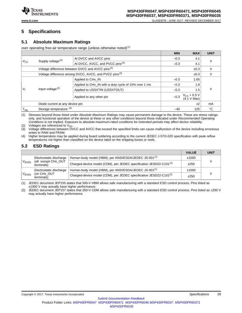
(1) Stresses beyond those listed under Absolute Maximum Ratings may cause permanent damage to the device. These are stress ratingsonly, and functional operation of the device at these or any other conditions beyond those indicated under Recommended OperatingConditions is not implied. Exposure to absolute-maximum-rated conditions for extended periods may affect device reliability.
(2) Voltages are referenced to VSS.(3) Voltage differences between DVCC and AVCC that exceed the specified limits can cause malfunction of the device including erroneous
writes to RAM and FRAM.(4) Higher temperature may be applied during board soldering according to the current JEDEC J-STD-020 specification with peak reflow
temperatures not higher than classified on the device label on the shipping boxes or reels.
5 Specifications
5.1 Absolute Maximum Ratingsover operating free-air temperature range (unless otherwise noted) (1)
MIN MAX UNIT
VCC Supply voltage (2) At DVCC and AVCC pins –0.3 4.1V
At DVCC, AVCC, and PVCC pins (2) –0.3 4.1Voltage difference between DVCC and AVCC pins (3) ±0.3 VVoltage difference among DVCC, AVCC, and PVCC pins (3) ±0.3 V
VI Input voltage (2)
Applied to CHx_IN –0.3 1.65
VApplied to CHx_IN with a duty cycle of 10% over 1 ms –0.3 1.8Applied to USSXTIN (USSXTOUT) –0.3 1.5
Applied to any other pin –0.3 VCC + 0.3 V(4.1 V Max)
Diode current at any device pin ±2 mATstg Storage temperature (4) –40 125 °C
(1) JEDEC document JEP155 states that 500-V HBM allows safe manufacturing with a standard ESD control process. Pins listed as±1000 V may actually have higher performance.
(2) JEDEC document JEP157 states that 250-V CDM allows safe manufacturing with a standard ESD control process. Pins listed as ±250 Vmay actually have higher performance.
5.2 ESD RatingsVALUE UNIT
V(ESD)
Electrostatic discharge(all except CHx_OUTterminals)
Human-body model (HBM), per ANSI/ESDA/JEDEC JS-001 (1) ±1000V
Charged-device model (CDM), per JEDEC specification JESD22-C101 (2) ±250
V(ESD)
Electrostatic discharge(on CHx_OUTterminals)
Human-body model (HBM), per ANSI/ESDA/JEDEC JS-001(1) ±1000VCharged-device model (CDM), per JEDEC specification JESD22-C101(2)
±250
30
MSP430FR6047, MSP430FR60471, MSP430FR6045MSP430FR6037, MSP430FR60371, MSP430FR6035SLASEB7B –JUNE 2017–REVISED DECEMBER 2017 www.ti.com
Submit Documentation FeedbackProduct Folder Links: MSP430FR6047 MSP430FR60471 MSP430FR6045 MSP430FR6037 MSP430FR60371
MSP430FR6035
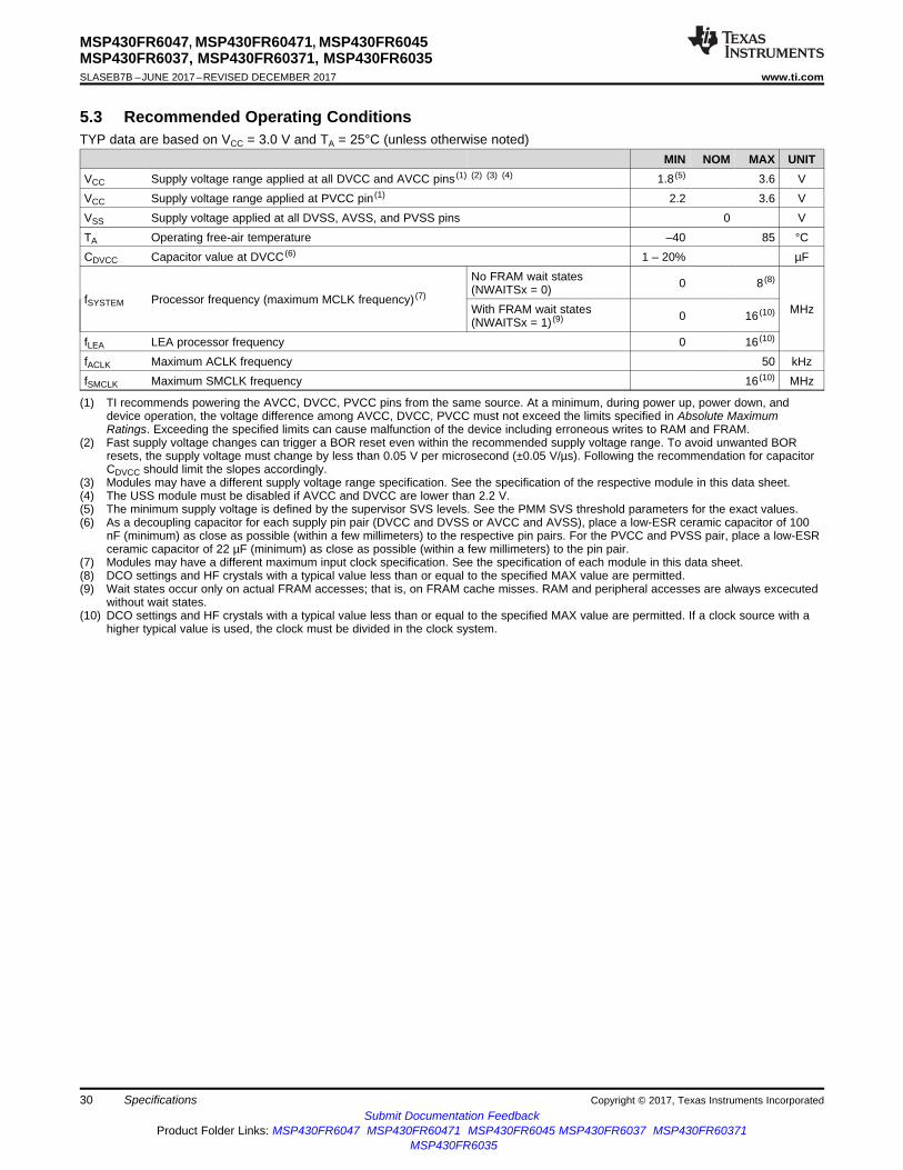
Specifications Copyright © 2017, Texas Instruments Incorporated
(1) TI recommends powering the AVCC, DVCC, PVCC pins from the same source. At a minimum, during power up, power down, anddevice operation, the voltage difference among AVCC, DVCC, PVCC must not exceed the limits specified in Absolute MaximumRatings. Exceeding the specified limits can cause malfunction of the device including erroneous writes to RAM and FRAM.
(2) Fast supply voltage changes can trigger a BOR reset even within the recommended supply voltage range. To avoid unwanted BORresets, the supply voltage must change by less than 0.05 V per microsecond (±0.05 V/µs). Following the recommendation for capacitorCDVCC should limit the slopes accordingly.
(3) Modules may have a different supply voltage range specification. See the specification of the respective module in this data sheet.(4) The USS module must be disabled if AVCC and DVCC are lower than 2.2 V.(5) The minimum supply voltage is defined by the supervisor SVS levels. See the PMM SVS threshold parameters for the exact values.(6) As a decoupling capacitor for each supply pin pair (DVCC and DVSS or AVCC and AVSS), place a low-ESR ceramic capacitor of 100
nF (minimum) as close as possible (within a few millimeters) to the respective pin pairs. For the PVCC and PVSS pair, place a low-ESRceramic capacitor of 22 µF (minimum) as close as possible (within a few millimeters) to the pin pair.
(7) Modules may have a different maximum input clock specification. See the specification of each module in this data sheet.(8) DCO settings and HF crystals with a typical value less than or equal to the specified MAX value are permitted.(9) Wait states occur only on actual FRAM accesses; that is, on FRAM cache misses. RAM and peripheral accesses are always excecuted
without wait states.(10) DCO settings and HF crystals with a typical value less than or equal to the specified MAX value are permitted. If a clock source with a
higher typical value is used, the clock must be divided in the clock system.
5.3 Recommended Operating ConditionsTYP data are based on VCC = 3.0 V and TA = 25°C (unless otherwise noted)
MIN NOM MAX UNITVCC Supply voltage range applied at all DVCC and AVCC pins (1) (2) (3) (4) 1.8 (5) 3.6 VVCC Supply voltage range applied at PVCC pin (1) 2.2 3.6 VVSS Supply voltage applied at all DVSS, AVSS, and PVSS pins 0 VTA Operating free-air temperature –40 85 °CCDVCC Capacitor value at DVCC (6) 1 – 20% µF
fSYSTEM Processor frequency (maximum MCLK frequency) (7)
No FRAM wait states(NWAITSx = 0) 0 8 (8)
MHzWith FRAM wait states(NWAITSx = 1) (9) 0 16 (10)
fLEA LEA processor frequency 0 16 (10)
fACLK Maximum ACLK frequency 50 kHzfSMCLK Maximum SMCLK frequency 16 (10) MHz

31
MSP430FR6047, MSP430FR60471, MSP430FR6045MSP430FR6037, MSP430FR60371, MSP430FR6035
www.ti.com SLASEB7B –JUNE 2017–REVISED DECEMBER 2017
Submit Documentation FeedbackProduct Folder Links: MSP430FR6047 MSP430FR60471 MSP430FR6045 MSP430FR6037 MSP430FR60371
MSP430FR6035
SpecificationsCopyright © 2017, Texas Instruments Incorporated
(1) All inputs are tied to 0 V or to VCC. Outputs do not source or sink any current.(2) Characterized with program executing typical data processing.
fACLK = 32768 Hz, fMCLK = fSMCLK = fDCO at specified frequency, except for 12 MHz. For 12 MHz, fDCO = 24 MHz andfMCLK = fSMCLK = fDCO/2.At MCLK frequencies above 8 MHz, the FRAM requires wait states. When wait states are required, the effective MCLK frequency(fMCLK,eff) decreases. The effective MCLK frequency also depends on the cache hit ratio. SMCLK is not affected by the number of waitstates or the cache hit ratio.The following equation can be used to compute fMCLK,eff:fMCLK,eff = fMCLK / [wait states × (1 – cache hit ratio) + 1]For example, with 1 wait state and 75% cache hit ratio, fMCKL,eff = fMCLK / [1 × (1 – 0.75) + 1] = fMCLK / 1.25.
(3) Represents typical program execution. Program and data reside entirely in FRAM. All execution is from FRAM.(4) Program resides in FRAM. Data resides in SRAM. Average current dissipation varies with cache hit-to-miss ratio as specified. Cache hit
ratio represents number cache accesess divided by the total number of FRAM accesses. For example, a 75% ratio implies three ofevery four accesses is from cache, and the remaining are FRAM accesses.
(5) See for typical curves. Each characteristic equation shown in the graph is computed using the least squares method for best linear fitusing the typical data shown in Section 5.4.
(6) Program and data reside entirely in RAM. All execution is from RAM.(7) Program and data reside entirely in RAM. All execution is from RAM. FRAM is off.
5.4 Active Mode Supply Current Into VCC Excluding External Currentover recommended operating free-air temperature (unless otherwise noted) (1) (2)
PARAMETER EXECUTIONMEMORY VCC
FREQUENCY (fMCLK = fSMCLK)
UNIT1 MHz0 WAITSTATES
(NWAITSx = 0)
4 MHz0 WAITSTATES
(NWAITSx = 0)
8 MHz0 WAITSTATES
(NWAITSx = 0)
12 MHz1 WAIT STATE(NWAITSx = 1)
16 MHz1 WAIT STATE(NWAITSx = 1)
TYP MAX TYP MAX TYP MAX TYP MAX TYP MAX
IAM, FRAM_UNI(Unified memory) (3) FRAM 3.0 V 225 665 1275 1550 1970 µA
IAM, FRAM (0%) (4) (5)FRAM
0% cache hitratio
3.0 V 420 1455 2850 2330 3000 µA
IAM, FRAM (50%) (4) (5)FRAM
50% cache hitratio
3.0 V 275 855 1022 1650 1888 1770 2041 2265 2606 µA
IAM, FRAM (66%) (4) (5)FRAM
66% cache hitratio
3.0 V 220 650 1240 1443 1490 1735 1880 2197 µA
IAM, FRAM (75%) (4) (5)FRAM
75% cache hitratio
3.0 V 192 261 535 1015 1170 1290 1490 1620 1870 µA
IAM, FRAM (100%) (4) (5)FRAM
100% cache hitratio
3.0 V 125 237 450 670 790 µA
IAM, RAM(6) (5) RAM 3.0 V 140 323 590 880 1070 µA
IAM, RAM only(7) (5) RAM 3.0 V 90 182 292 540 830 1020 1313 µA

0
500
1000
1500
2000
2500
3000
0 1 2 3 4 5 6 7 8 9
Active
Mode
Curr
ent (µ
A)
MCLK Frequency (MHz)
I(AM,0%)
I(AM,50%)
I(AM,66%)
I(AM,75%)
I(AM,100%)
I(AM,RAMonly)
I(AM,75%)[µA] ~ 120 f[MHz] + 68×
32
MSP430FR6047, MSP430FR60471, MSP430FR6045MSP430FR6037, MSP430FR60371, MSP430FR6035SLASEB7B –JUNE 2017–REVISED DECEMBER 2017 www.ti.com
Submit Documentation FeedbackProduct Folder Links: MSP430FR6047 MSP430FR60471 MSP430FR6045 MSP430FR6037 MSP430FR60371
MSP430FR6035
Specifications Copyright © 2017, Texas Instruments Incorporated
5.5 Typical Characteristics, Active Mode Supply Currents
A. I(AM,cache hit ratio): Program resides in FRAM. Data resides in SRAM. Average current dissipation varies with cache hit-to-miss ratio as specified. Cache hit ratio represents number cache accesses divided by the total number of FRAMaccesses. For example, a 75% ratio implies three of every four accesses is from cache, and the remaining are FRAMaccesses.
B. I(AM,RAMonly): Program and data reside entirely in RAM. All execution is from RAM. FRAM is off.
Figure 5-1. Typical Active Mode Supply Currents, No Wait States
(1) All inputs are tied to 0 V or to VCC. Outputs do not source or sink any current.(2) Current for watchdog timer clocked by SMCLK included.
fACLK = 32768 Hz, fMCLK = 0 MHz, fSMCLK = fDCO at specified frequency, except for 12 MHz. For 12 MHz, fDCO = 24 MHz andfMCLK = fSMCLK = fDCO / 2.
5.6 Low-Power Mode (LPM0, LPM1) Supply Currents Into VCC Excluding External Currentover recommended operating free-air temperature (unless otherwise noted) (1) (2)
PARAMETER VCC
FREQUENCY (fSMCLK)UNIT1 MHz 4 MHz 8 MHz 12 MHz 16 MHz
TYP MAX TYP MAX TYP MAX TYP MAX TYP MAX
ILPM02.2 V 80 115 180 276 250
µA3.0 V 95 148 125 178 190 245 286 340 265 316
ILPM12.2 V 40 70 136 230 205
µA3.0 V 40 70 70 136 235 210 250

33
MSP430FR6047, MSP430FR60471, MSP430FR6045MSP430FR6037, MSP430FR60371, MSP430FR6035
www.ti.com SLASEB7B –JUNE 2017–REVISED DECEMBER 2017
Submit Documentation FeedbackProduct Folder Links: MSP430FR6047 MSP430FR60471 MSP430FR6045 MSP430FR6037 MSP430FR60371
MSP430FR6035
SpecificationsCopyright © 2017, Texas Instruments Incorporated
(1) Not applicable for devices with HF crystal oscillator only.(2) Characterized with a Micro Crystal MS1V-T1K crystal with a load capacitance of 12.5 pF. The internal and external load capacitance are
chosen to closely match the required 12.5‑pF load.(3) Low-power mode 2, crystal oscillator test conditions:
Current for watchdog timer clocked by ACLK and RTC clocked by XT1 included. Current for brownout and SVS included.CPUOFF = 1, SCG0 = 0 SCG1 = 1, OSCOFF = 0 (LPM2), fXT1 = 32768 Hz, fACLK = fXT1, fMCLK = fSMCLK = 0 MHz
(4) Characterized with a Seiko SSP-T7-FL (SMD) crystal with a load capacitance of 3.7 pF. The internal and external load capacitance arechosen to closely match the required 3.7‑pF load.
(5) Low-power mode 2, VLO test conditions:Current for watchdog timer clocked by ACLK included. RTC disabled (RTCHOLD = 1). Current for brownout and SVS included.CPUOFF = 1, SCG0 = 0 SCG1 = 1, OSCOFF = 0 (LPM2), fXT1 = 0 Hz, fACLK = fVLO, fMCLK = fSMCLK = 0 MHz
(6) Low-power mode 3, 12‑pF crystal including SVS test conditions:Current for watchdog timer clocked by ACLK and RTC clocked by XT1 included. Current for brownout and SVS included (SVSHE = 1).CPUOFF = 1, SCG0 = 1 SCG1 = 1, OSCOFF = 0 (LPM3), fXT1 = 32768 Hz, fACLK = fXT1, fMCLK = fSMCLK = 0 MHzActivating additional peripherals increases the current consumption due to active supply current contribution as well as due to additionalidle current. Refer to the idle currents specified for the respective peripheral groups.
(7) Low-power mode 3, 3.7‑pF crystal excluding SVS test conditions:Current for watchdog timer clocked by ACLK and RTC clocked by XT1 included. Current for brownout included. SVS disabled (SVSHE =0).CPUOFF = 1, SCG0 = 1 SCG1 = 1, OSCOFF = 0 (LPM3), fXT1 = 32768 Hz, fACLK = fXT1, fMCLK = fSMCLK = 0 MHzActivating additional peripherals increases the current consumption due to active supply current contribution as well as due to additionalidle current. Refer to the idle currents specified for the respective peripheral groups.
(8) Low-power mode 3, VLO excluding SVS test conditions:Current for watchdog timer clocked by ACLK included. RTC disabled (RTCHOLD = 1). RAM disabled (RCCTL0 = 5A55h). Current forbrownout included. SVS disabled (SVSHE = 0).CPUOFF = 1, SCG0 = 1 SCG1 = 1, OSCOFF = 0 (LPM3), fXT1 = 0 Hz, fACLK = fVLO, fMCLK = fSMCLK = 0 MHzActivating additional peripherals increases the current consumption due to active supply current contribution as well as due to additionalidle current. Refer to the idle currents specified for the respective peripheral groups.
(9) Low-power mode 4 including SVS test conditions:Current for brownout and SVS included (SVSHE = 1).CPUOFF = 1, SCG0 = 1 SCG1 = 1, OSCOFF = 1 (LPM4), fXT1 = 0 Hz, fACLK = 0 Hz, fMCLK = fSMCLK = 0 MHzActivating additional peripherals increases the current consumption due to active supply current contribution as well as due to additionalidle current. Refer to the idle currents specified for the respective peripheral groups.
5.7 Low-Power Mode (LPM2, LPM3, LPM4) Supply Currents (Into VCC) Excluding ExternalCurrent
over recommended ranges of supply voltage and operating free-air temperature (unless otherwise noted) (see Figure 5-2 andFigure 5-3)
PARAMETERTEMPERATURE
UNITVCC
–40°C 25°C 60°C 85°CTYP MAX TYP MAX TYP MAX TYP MAX
ILPM2,XT12Low-power mode 2, 12‑pFcrystal (1) (2) (3)
2.2 V 0.8 1.3 4.1 10.8μA
3 V 0.8 1.3 4.1 10.8
ILPM2,XT3.7Low-power mode 2, 3.7‑pFcrystal (1) (4) (3)
2.2 V 0.6 1.2 4.0 10.7μA
3 V 0.6 1.2 4.0 10.7
ILPM2,VLOLow-power mode 2, VLO,includes SVS (5)
2.2 V 0.5 1.0 3.8 10.5μA
3 V 0.5 1.0 3.8 10.5
ILPM3,XT12
Low-power mode 3, 12‑pFcrystal, includes SVS (1) (2)(6)
2.2 V 0.8 1.1 1.0 2.2 4.5 10.1μA
3 V 0.8 1.0 2.2 4.5
ILPM3,XT3.7
Low-power mode 3, 3.7‑pFcrystal, excludes SVS (1) (4)(7)
2.2 V 0.5 0.7 2.1 4.4 9.8μA
3 V 0.5 0.7 2.1 4.4 9.8
ILPM3,VLOLow-power mode 3,VLO, excludes SVS (8)
2.2 V 0.4 0.5 1.2 1.9 4.2 9.6μA
3 V 0.4 0.5 1.9 4.2
ILPM3,VLO,RAMoff
Low-power mode 3,VLO, excludes SVS, RAMpowered-downcompletely (8)
2.2 V 0.36 0.47 1.1 1.4 2.9 2.6 8.2
μA3 V 0.36 0.47 1.4 2.6
ILPM4,SVSLow-power mode 4,includes SVS (9)
2.2 V 0.5 0.6 1.2 1.9 4.3 9.7μA
3 V 0.5 0.8 0.6 1.9 4.3
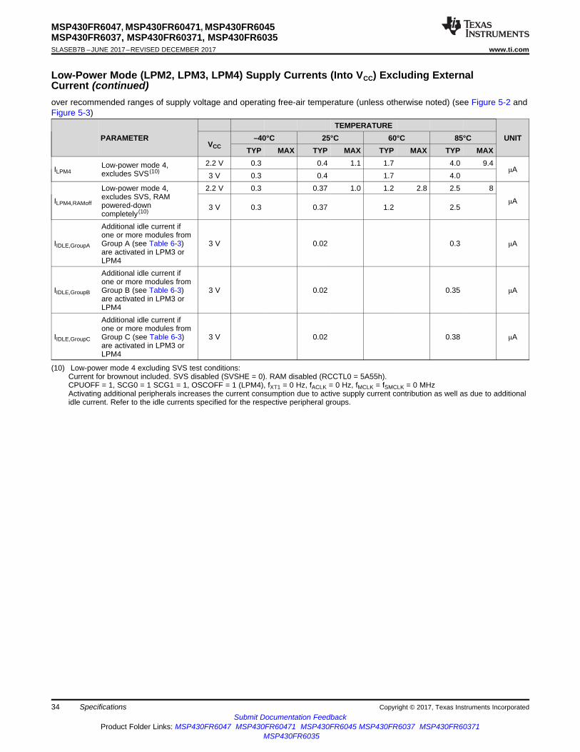
34
MSP430FR6047, MSP430FR60471, MSP430FR6045MSP430FR6037, MSP430FR60371, MSP430FR6035SLASEB7B –JUNE 2017–REVISED DECEMBER 2017 www.ti.com
Submit Documentation FeedbackProduct Folder Links: MSP430FR6047 MSP430FR60471 MSP430FR6045 MSP430FR6037 MSP430FR60371
MSP430FR6035
Specifications Copyright © 2017, Texas Instruments Incorporated
Low-Power Mode (LPM2, LPM3, LPM4) Supply Currents (Into VCC) Excluding ExternalCurrent (continued)over recommended ranges of supply voltage and operating free-air temperature (unless otherwise noted) (see Figure 5-2 andFigure 5-3)
PARAMETERTEMPERATURE
UNITVCC
–40°C 25°C 60°C 85°CTYP MAX TYP MAX TYP MAX TYP MAX
(10) Low-power mode 4 excluding SVS test conditions:Current for brownout included. SVS disabled (SVSHE = 0). RAM disabled (RCCTL0 = 5A55h).CPUOFF = 1, SCG0 = 1 SCG1 = 1, OSCOFF = 1 (LPM4), fXT1 = 0 Hz, fACLK = 0 Hz, fMCLK = fSMCLK = 0 MHzActivating additional peripherals increases the current consumption due to active supply current contribution as well as due to additionalidle current. Refer to the idle currents specified for the respective peripheral groups.
ILPM4Low-power mode 4,excludes SVS (10)
2.2 V 0.3 0.4 1.1 1.7 4.0 9.4μA
3 V 0.3 0.4 1.7 4.0
ILPM4,RAMoff
Low-power mode 4,excludes SVS, RAMpowered-downcompletely (10)
2.2 V 0.3 0.37 1.0 1.2 2.8 2.5 8
μA3 V 0.3 0.37 1.2 2.5
IIDLE,GroupA
Additional idle current ifone or more modules fromGroup A (see Table 6-3)are activated in LPM3 orLPM4
3 V 0.02 0.3 μA
IIDLE,GroupB
Additional idle current ifone or more modules fromGroup B (see Table 6-3)are activated in LPM3 orLPM4
3 V 0.02 0.35 μA
IIDLE,GroupC
Additional idle current ifone or more modules fromGroup C (see Table 6-3)are activated in LPM3 orLPM4
3 V 0.02 0.38 μA
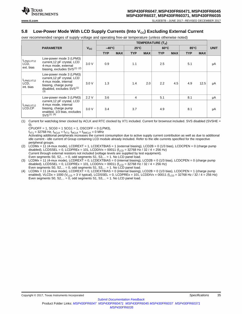
35
MSP430FR6047, MSP430FR60471, MSP430FR6045MSP430FR6037, MSP430FR60371, MSP430FR6035
www.ti.com SLASEB7B –JUNE 2017–REVISED DECEMBER 2017
Submit Documentation FeedbackProduct Folder Links: MSP430FR6047 MSP430FR60471 MSP430FR6045 MSP430FR6037 MSP430FR60371
MSP430FR6035
SpecificationsCopyright © 2017, Texas Instruments Incorporated
(1) Current for watchdog timer clocked by ACLK and RTC clocked by XT1 included. Current for brownout included. SVS disabled (SVSHE =0).CPUOFF = 1, SCG0 = 1 SCG1 = 1, OSCOFF = 0 (LPM3),fXT1 = 32768 Hz, fACLK = fXT1, fMCLK = fSMCLK = 0 MHzActivating additional peripherals increases the current consumption due to active supply current contribution as well as due to additionalidle current - idle current of Group containing LCD module already included. Refer to the idle currents specified for the respectiveperipheral groups.
(2) LCDMx = 11 (4-mux mode), LCDREXT = 1, LCDEXTBIAS = 1 (external biasing), LCD2B = 0 (1/3 bias), LCDCPEN = 0 (charge pumpdisabled), LCDSSEL = 0, LCDPREx = 101, LCDDIVx = 00011 (fLCD = 32768 Hz / 32 / 4 = 256 Hz)Current through external resistors not included (voltage levels are supplied by test equipment).Even segments S0, S2,... = 0, odd segments S1, S3,... = 1. No LCD panel load.
(3) LCDMx = 11 (4-mux mode), LCDREXT = 0, LCDEXTBIAS = 0 (internal biasing), LCD2B = 0 (1/3 bias), LCDCPEN = 0 (charge pumpdisabled), LCDSSEL = 0, LCDPREx = 101, LCDDIVx = 00011 (fLCD = 32768 Hz / 32 / 4 = 256 Hz)Even segments S0, S2,... = 0, odd segments S1, S3,... = 1. No LCD panel load.
(4) LCDMx = 11 (4-mux mode), LCDREXT = 0, LCDEXTBIAS = 0 (internal biasing), LCD2B = 0 (1/3 bias), LCDCPEN = 1 (charge pumpenabled), VLCDx = 1000 (VLCD = 3 V typical), LCDSSEL = 0, LCDPREx = 101, LCDDIVx = 00011 (fLCD = 32768 Hz / 32 / 4 = 256 Hz)Even segments S0, S2,... = 0, odd segments S1, S3,... = 1. No LCD panel load.
5.8 Low-Power Mode With LCD Supply Currents (Into VCC) Excluding External Currentover recommended ranges of supply voltage and operating free-air temperature (unless otherwise noted)
PARAMETER VCC
TEMPERATURE (TA)UNIT–40°C 25°C 60°C 85°C
TYP MAX TYP MAX TYP MAX TYP MAX
ILPM3,XT12LCD,ext. bias
Low-power mode 3 (LPM3)current,12 pF crystal, LCD4-mux mode, externalbiasing, excludes SVS (1) (2)
3.0 V 0.9 1.1 2.5 5.1 µA
ILPM3,XT12LCD,int. bias
Low-power mode 3 (LPM3)current,12 pF crystal, LCD4-mux mode, internalbiasing, charge pumpdisabled, excludes SVS (1)(3)
3.0 V 1.3 1.4 2.0 2.2 4.5 4.9 12.5 µA
ILPM3,XT12LCD,CP
Low-power mode 3 (LPM3)current,12 pF crystal, LCD4-mux mode, internalbiasing, charge pumpenabled, 1/3 bias, excludesSVS (1) (4)
2.2 V 3.6 4 5.1 8.1 µA
3.0 V 3.4 3.7 4.9 8.1 µA

36
MSP430FR6047, MSP430FR60471, MSP430FR6045MSP430FR6037, MSP430FR60371, MSP430FR6035SLASEB7B –JUNE 2017–REVISED DECEMBER 2017 www.ti.com
Submit Documentation FeedbackProduct Folder Links: MSP430FR6047 MSP430FR60471 MSP430FR6045 MSP430FR6037 MSP430FR60371
MSP430FR6035
Specifications Copyright © 2017, Texas Instruments Incorporated
(1) Not applicable for devices with HF crystal oscillator only.(2) Characterized with a Micro Crystal MS1V-T1K crystal with a load capacitance of 12.5 pF. The internal and external load capacitance are
chosen to closely match the required 12.5‑pF load.(3) Low-power mode 3.5, 1‑pF crystal including SVS test conditions:
Current for RTC clocked by XT1 included. Current for brownout and SVS included (SVSHE = 1). Core regulator disabled.PMMREGOFF = 1, CPUOFF = 1, SCG0 = 1 SCG1 = 1, OSCOFF = 1 (LPMx.5),fXT1 = 32768 Hz, fACLK = fXT1, fMCLK = fSMCLK = 0 MHz
(4) Characterized with a Seiko SSP-T7-FL (SMD) crystal with a load capacitance of 3.7 pF. The internal and external load capacitance arechosen to closely match the required 3.7‑pF load.
(5) Low-power mode 3.5, 3.7‑pF crystal excluding SVS test conditions:Current for RTC clocked by XT1 included.Current for brownout included. SVS disabled (SVSHE = 0). Core regulator disabled.PMMREGOFF = 1, CPUOFF = 1, SCG0 = 1 SCG1 = 1, OSCOFF = 1 (LPMx.5),fXT1 = 32768 Hz, fACLK = fXT1, fMCLK = fSMCLK = 0 MHz
(6) Low-power mode 4.5 including SVS test conditions:Current for brownout and SVS included (SVSHE = 1). Core regulator disabled.PMMREGOFF = 1, CPUOFF = 1, SCG0 = 1 SCG1 = 1, OSCOFF = 1 (LPMx.5),fXT1 = 0 Hz, fACLK = 0 Hz, fMCLK = fSMCLK = 0 MHz
(7) Low-power mode 4.5 excluding SVS test conditions:Current for brownout included. SVS disabled (SVSHE = 0). Core regulator disabled.PMMREGOFF = 1, CPUOFF = 1, SCG0 = 1 SCG1 = 1, OSCOFF = 1 (LPMx.5),fXT1 = 0 Hz, fACLK = 0 Hz, fMCLK = fSMCLK = 0 MHz
5.9 Low-Power Mode (LPMx.5) Supply Currents (Into VCC) Excluding External Currentover recommended ranges of supply voltage and operating free-air temperature (unless otherwise noted) (see Figure 5-4 andFigure 5-5)
PARAMETER VCC
TEMPERTURE (TA)UNIT–40°C 25°C 60°C 85°C
TYP MAX TYP MAX TYP MAX TYP MAX
ILPM3.5,XT12
Low-power mode 3.5,12‑pF crystal includingSVS (1) (2) (3)
2.2 V 0.45 0.5 0.55 0.75μA
3.0 V 0.45 0.5 0.55 0.75
ILPM3.5,XT3.7
Low-power mode 3.5,3.7‑pF crystal excludingSVS (1) (4) (5)
2.2 V 0.3 0.35 0.4 0.65μA
3.0 V 0.3 0.35 0.4 0.65
ILPM4.5,SVSLow-power mode 4.5,including SVS (6)
2.2 V 0.23 0.2 0.28 0.4μA
3.0 V 0.23 0.2 0.28 0.4
ILPM4.5Low-power mode 4.5,excluding SVS (7)
2.2 V 0.035 0.045 0.075 0.15μA
3.0 V 0.035 0.045 0.075 0.15
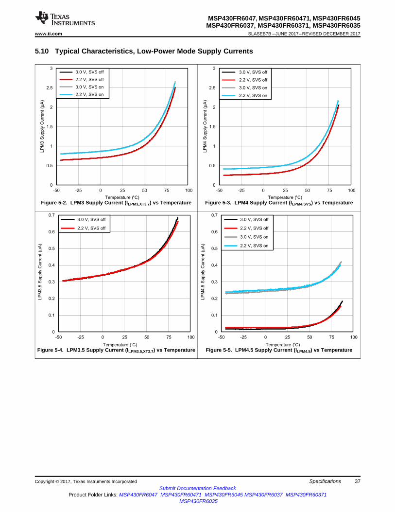
0
0.1
0.2
0.3
0.4
0.5
0.6
0.7
-50 -25 0 25 50 75 100
3.0 V, SVS off
2.2 V, SVS off
LP
M3.5
Supply
Curr
ent
(µA
)
Temperature (°C)
0
0.1
0.2
0.3
0.4
0.5
0.6
0.7
-50 -25 0 25 50 75 100
3.0 V, SVS off
2.2 V, SVS off
3.0 V, SVS on
2.2 V, SVS on
LP
M4.5
Supply
Curr
ent
(µA
)
Temperature (°C)
0
0.5
1
1.5
2
2.5
3
-50 -25 0 25 50 75 100
LP
M3
Supply
Curr
ent
(µA
)
Temperature (°C)
3.0 V, SVS off
2.2 V, SVS off
3.0 V, SVS on
2.2 V, SVS on
0
0.5
1
1.5
2
2.5
3
-50 -25 0 25 50 75 100
LP
M4
Supply
Curr
ent
(µA
)
Temperature (°C)
3.0 V, SVS off
2.2 V, SVS off
3.0 V, SVS on
2.2 V, SVS on
37
MSP430FR6047, MSP430FR60471, MSP430FR6045MSP430FR6037, MSP430FR60371, MSP430FR6035
www.ti.com SLASEB7B –JUNE 2017–REVISED DECEMBER 2017
Submit Documentation FeedbackProduct Folder Links: MSP430FR6047 MSP430FR60471 MSP430FR6045 MSP430FR6037 MSP430FR60371
MSP430FR6035
SpecificationsCopyright © 2017, Texas Instruments Incorporated
5.10 Typical Characteristics, Low-Power Mode Supply Currents
Figure 5-2. LPM3 Supply Current (ILPM3,XT3.7) vs Temperature Figure 5-3. LPM4 Supply Current (ILPM4,SVS) vs Temperature
Figure 5-4. LPM3.5 Supply Current (ILPM3.5,XT3.7) vs Temperature Figure 5-5. LPM4.5 Supply Current (ILPM4.5) vs Temperature

38
MSP430FR6047, MSP430FR60471, MSP430FR6045MSP430FR6037, MSP430FR60371, MSP430FR6035SLASEB7B –JUNE 2017–REVISED DECEMBER 2017 www.ti.com
Submit Documentation FeedbackProduct Folder Links: MSP430FR6047 MSP430FR60471 MSP430FR6045 MSP430FR6037 MSP430FR60371
MSP430FR6035
Specifications Copyright © 2017, Texas Instruments Incorporated
(1) For other module currents not listed here, see the module-specific parameter sections.
5.11 Typical Characteristics, Current Consumption per Module (1)
MODULE TEST CONDITIONS REFERENCE CLOCK MIN TYP MAX UNITTimer_A Module input clock 2.5 μA/MHzTimer_B Module input clock 3.8 μA/MHz
eUSCI_AUART mode
Module input clock6.3 7.0
μA/MHzSPI mode 4.4 4.8
eUSCI_BSPI mode
Module input clock4.4
μA/MHzI2C mode, 100 kbaud 4.4
RTC_C 32 kHz 100 nAMPY Only from start to end of operation MCLK 28 μA/MHzCRC16 Only from start to end of operation MCLK 3.3 μA/MHzCRC32 Only from start to end of operation MCLK 3.3 μA/MHz
LEA256-point complex FFT, data = nonzero
MCLK68 86
µA/MHz256-point complex FFT, data = zero 66
MTIF Generator and counter are enabled at 256 Hz, noterminal activity, pulse rate = 15 pulses LFXT 0.20 µA
(1) N/A = not applicable(2) For more information about traditional and new thermal metrics, see Semiconductor and IC Package Thermal Metrics.(3) These values are based on a JEDEC-defined 2S2P system (with the exception of the Theta JC (RθJC) value, which is based on a
JEDEC-defined 1S0P system) and will change based on environment and application. For more information, see these EIA/JEDECstandards:• JESD51-2, Integrated Circuits Thermal Test Method Environmental Conditions - Natural Convection (Still Air)• JESD51-3, Low Effective Thermal Conductivity Test Board for Leaded Surface Mount Packages• JESD51-7, High Effective Thermal Conductivity Test Board for Leaded Surface Mount Packages• JESD51-9, Test Boards for Area Array Surface Mount Package Thermal Measurements
5.12 Thermal Resistance Characteristics for 100-Pin LQFP (PZ) Package (1)
THERMAL METRIC (2) VALUE (3) UNITRθJA Junction-to-ambient thermal resistance, still air 57.6 °C/WRθJC(TOP) Junction-to-case (top) thermal resistance 14.9 °C/WRθJB Junction-to-board thermal resistance 35.6 °C/WΨJB Junction-to-board thermal characterization parameter 35.0 °C/WΨJT Junction-to-top thermal characterization parameter 0.6 °C/WRθJC(BOTTOM) Junction-to-case (bottom) thermal resistance N/A °C/W

39
MSP430FR6047, MSP430FR60471, MSP430FR6045MSP430FR6037, MSP430FR60371, MSP430FR6035
www.ti.com SLASEB7B –JUNE 2017–REVISED DECEMBER 2017
Submit Documentation FeedbackProduct Folder Links: MSP430FR6047 MSP430FR60471 MSP430FR6045 MSP430FR6037 MSP430FR60371
MSP430FR6035
SpecificationsCopyright © 2017, Texas Instruments Incorporated
5.13 Timing and Switching Characteristics
5.13.1 Power Supply SequencingTI recommends powering the AVCC, DVCC, and PVCC pins from the same source. At a minimum, duringpower up, power down, and device operation, the voltage difference among AVCC, DVCC, and PVCCmust not exceed the limits specified in Section 5.1. Exceeding the specified limits can cause malfunctionof the device including erroneous writes to RAM and FRAM.
Table 5-1 lists the power ramp requirements for brownout and power up.
(1) Fast supply voltage changes can trigger a BOR reset even within the recommended supply voltage range. To avoid unwanted BORresets, the supply voltage must change by less than 0.05 V per microsecond (±0.05 V/µs). Following the recommendation for capacitorCDVCC should limit the slopes accordingly.
(2) The brownout levels are measured with a slowly changing supply.
Table 5-1. Brownout and Device Reset Power Ramp Requirementsover recommended ranges of supply voltage and operating free-air temperature (unless otherwise noted)
PARAMETER TEST CONDITIONS MIN MAX UNITVVCC_BOR– Brownout power-down level (1) | dDVCC/dt | < 3 V/s 0.7 1.66 VVVCC_BOR+ Brownout power-up level (1) | dDVCC/dt | < 3 V/s (2) 0.79 1.68 V
Table 5-2 lists the characteristics of the SVS.
Table 5-2. SVSover recommended ranges of supply voltage and operating free-air temperature (unless otherwise noted)
PARAMETER TEST CONDITIONS MIN TYP MAX UNITISVSH,LPM SVSH current consumption, low-power modes 170 300 nAVSVSH– SVSH power-down level 1.75 1.80 1.85 VVSVSH+ SVSH power-up level 1.77 1.88 1.99 VVSVSH_hys SVSH hysteresis 40 120 mVtPD,SVSH, AM SVSH propagation delay, active mode dVVcc/dt = –10 mV/µs 10 µs
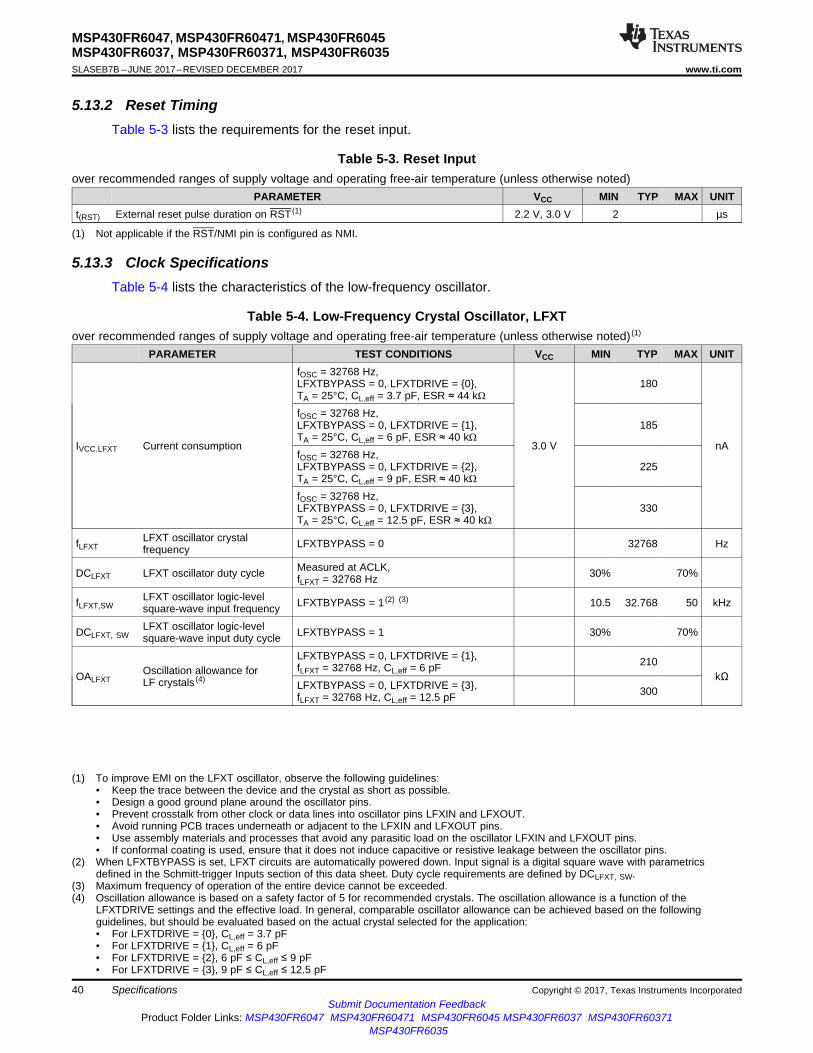
40
MSP430FR6047, MSP430FR60471, MSP430FR6045MSP430FR6037, MSP430FR60371, MSP430FR6035SLASEB7B –JUNE 2017–REVISED DECEMBER 2017 www.ti.com
Submit Documentation FeedbackProduct Folder Links: MSP430FR6047 MSP430FR60471 MSP430FR6045 MSP430FR6037 MSP430FR60371
MSP430FR6035
Specifications Copyright © 2017, Texas Instruments Incorporated
5.13.2 Reset TimingTable 5-3 lists the requirements for the reset input.
(1) Not applicable if the RST/NMI pin is configured as NMI.
Table 5-3. Reset Inputover recommended ranges of supply voltage and operating free-air temperature (unless otherwise noted)
PARAMETER VCC MIN TYP MAX UNITt(RST) External reset pulse duration on RST (1) 2.2 V, 3.0 V 2 µs
5.13.3 Clock SpecificationsTable 5-4 lists the characteristics of the low-frequency oscillator.
(1) To improve EMI on the LFXT oscillator, observe the following guidelines:• Keep the trace between the device and the crystal as short as possible.• Design a good ground plane around the oscillator pins.• Prevent crosstalk from other clock or data lines into oscillator pins LFXIN and LFXOUT.• Avoid running PCB traces underneath or adjacent to the LFXIN and LFXOUT pins.• Use assembly materials and processes that avoid any parasitic load on the oscillator LFXIN and LFXOUT pins.• If conformal coating is used, ensure that it does not induce capacitive or resistive leakage between the oscillator pins.
(2) When LFXTBYPASS is set, LFXT circuits are automatically powered down. Input signal is a digital square wave with parametricsdefined in the Schmitt-trigger Inputs section of this data sheet. Duty cycle requirements are defined by DCLFXT, SW.
(3) Maximum frequency of operation of the entire device cannot be exceeded.(4) Oscillation allowance is based on a safety factor of 5 for recommended crystals. The oscillation allowance is a function of the
LFXTDRIVE settings and the effective load. In general, comparable oscillator allowance can be achieved based on the followingguidelines, but should be evaluated based on the actual crystal selected for the application:• For LFXTDRIVE = 0, CL,eff = 3.7 pF• For LFXTDRIVE = 1, CL,eff = 6 pF• For LFXTDRIVE = 2, 6 pF ≤ CL,eff ≤ 9 pF• For LFXTDRIVE = 3, 9 pF ≤ CL,eff ≤ 12.5 pF
Table 5-4. Low-Frequency Crystal Oscillator, LFXTover recommended ranges of supply voltage and operating free-air temperature (unless otherwise noted) (1)
PARAMETER TEST CONDITIONS VCC MIN TYP MAX UNIT
IVCC.LFXT Current consumption
fOSC = 32768 Hz,LFXTBYPASS = 0, LFXTDRIVE = 0,TA = 25°C, CL,eff = 3.7 pF, ESR ≈ 44 kΩ
3.0 V
180
nA
fOSC = 32768 Hz,LFXTBYPASS = 0, LFXTDRIVE = 1,TA = 25°C, CL,eff = 6 pF, ESR ≈ 40 kΩ
185
fOSC = 32768 Hz,LFXTBYPASS = 0, LFXTDRIVE = 2,TA = 25°C, CL,eff = 9 pF, ESR ≈ 40 kΩ
225
fOSC = 32768 Hz,LFXTBYPASS = 0, LFXTDRIVE = 3,TA = 25°C, CL,eff = 12.5 pF, ESR ≈ 40 kΩ
330
fLFXTLFXT oscillator crystalfrequency LFXTBYPASS = 0 32768 Hz
DCLFXT LFXT oscillator duty cycle Measured at ACLK,fLFXT = 32768 Hz 30% 70%
fLFXT,SWLFXT oscillator logic-levelsquare-wave input frequency LFXTBYPASS = 1 (2) (3) 10.5 32.768 50 kHz
DCLFXT, SWLFXT oscillator logic-levelsquare-wave input duty cycle LFXTBYPASS = 1 30% 70%
OALFXTOscillation allowance forLF crystals (4)
LFXTBYPASS = 0, LFXTDRIVE = 1,fLFXT = 32768 Hz, CL,eff = 6 pF 210
kΩLFXTBYPASS = 0, LFXTDRIVE = 3,fLFXT = 32768 Hz, CL,eff = 12.5 pF 300
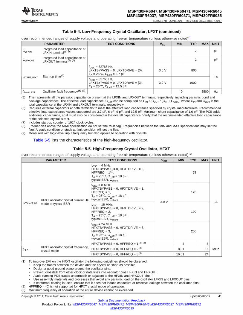
41
MSP430FR6047, MSP430FR60471, MSP430FR6045MSP430FR6037, MSP430FR60371, MSP430FR6035
www.ti.com SLASEB7B –JUNE 2017–REVISED DECEMBER 2017
Submit Documentation FeedbackProduct Folder Links: MSP430FR6047 MSP430FR60471 MSP430FR6045 MSP430FR6037 MSP430FR60371
MSP430FR6035
SpecificationsCopyright © 2017, Texas Instruments Incorporated
Table 5-4. Low-Frequency Crystal Oscillator, LFXT (continued)over recommended ranges of supply voltage and operating free-air temperature (unless otherwise noted)(1)
PARAMETER TEST CONDITIONS VCC MIN TYP MAX UNIT
(5) This represents all the parasitic capacitance present at the LFXIN and LFXOUT terminals, respectively, including parasitic bond andpackage capacitance. The effective load capacitance, CL,eff can be computed as CIN × COUT / (CIN + COUT), where CIN and COUT is thetotal capacitance at the LFXIN and LFXOUT terminals, respectively.
(6) Requires external capacitors at both terminals to meet the effective load capacitance specified by crystal manufacturers. Recommendedeffective load capacitance values supported are 3.7 pF, 6 pF, 9 pF, and 12.5 pF. Maximum shunt capacitance of 1.6 pF. The PCB addsadditional capacitance, so it must also be considered in the overall capacitance. Verify that the recommended effective load capacitanceof the selected crystal is met.
(7) Includes start-up counter of 1024 clock cycles.(8) Frequencies above the MAX specification do not set the fault flag. Frequencies between the MIN and MAX specifications may set the
flag. A static condition or stuck at fault condition will set the flag.(9) Measured with logic-level input frequency but also applies to operation with crystals.
CLFXINIntegrated load capacitance atLFXIN terminal (5) (6) 2 pF
CLFXOUTIntegrated load capacitance atLFXOUT terminal (5) (6) 2 pF
tSTART,LFXT Start-up time (7)
fOSC = 32768 Hz,LFXTBYPASS = 0, LFXTDRIVE = 0,TA = 25°C, CL,eff = 3.7 pF
3.0 V 800
msfOSC = 32768 Hz,LFXTBYPASS = 0, LFXTDRIVE = 3,TA = 25°C, CL,eff = 12.5 pF
3.0 V 1000
fFault,LFXT Oscillator fault frequency (8) (9) 0 3500 Hz
Table 5-5 lists the characteristics of the high-frequency oscillator.
(1) To improve EMI on the HFXT oscillator the following guidelines should be observed.• Keep the traces between the device and the crystal as short as possible.• Design a good ground plane around the oscillator pins.• Prevent crosstalk from other clock or data lines into oscillator pins HFXIN and HFXOUT.• Avoid running PCB traces underneath or adjacent to the HFXIN and HFXOUT pins.• Use assembly materials and processes that avoid any parasitic load on the oscillator LFXIN and LFXOUT pins.• If conformal coating is used, ensure that it does not induce capacitive or resistive leakage between the oscillator pins.
(2) HFFREQ = 0 is not supported for HFXT crystal mode of operation.(3) Maximum frequency of operation of the entire device cannot be exceeded.
Table 5-5. High-Frequency Crystal Oscillator, HFXTover recommended ranges of supply voltage and operating free-air temperature (unless otherwise noted) (1)
PARAMETER TEST CONDITIONS VCC MIN TYP MAX UNIT
IDVCC.HFXTHFXT oscillator crystal current HFmode at typical ESR
fOSC = 4 MHz,HFXTBYPASS = 0, HFXTDRIVE = 0,HFFREQ = 1 (2),TA = 25°C, CL,eff = 18 pF,typical ESR, Cshunt
3.0 V
75
μA
fOSC = 8 MHz,HFXTBYPASS = 0, HFXTDRIVE = 1,HFFREQ = 1,TA = 25°C, CL,eff = 18 pF,typical ESR, Cshunt
120
fOSC = 16 MHz,HFXTBYPASS = 0, HFXTDRIVE = 2,HFFREQ = 2,TA = 25°C, CL,eff = 18 pF,typical ESR, Cshunt
190
fOSC = 24 MHzHFXTBYPASS = 0, HFXTDRIVE = 3,HFFREQ = 3,TA = 25°C, CL,eff = 18 pF,typical ESR, Cshunt
250
fHFXTHFXT oscillator crystal frequency,crystal mode
HFXTBYPASS = 0, HFFREQ = 1 (2) (3) 4 8MHzHFXTBYPASS = 0, HFFREQ = 2 (3) 8.01 16
HFXTBYPASS = 0, HFFREQ = 3 (3) 16.01 24

42
MSP430FR6047, MSP430FR60471, MSP430FR6045MSP430FR6037, MSP430FR60371, MSP430FR6035SLASEB7B –JUNE 2017–REVISED DECEMBER 2017 www.ti.com
Submit Documentation FeedbackProduct Folder Links: MSP430FR6047 MSP430FR60471 MSP430FR6045 MSP430FR6037 MSP430FR60371
MSP430FR6035
Specifications Copyright © 2017, Texas Instruments Incorporated
Table 5-5. High-Frequency Crystal Oscillator, HFXT (continued)over recommended ranges of supply voltage and operating free-air temperature (unless otherwise noted)(1)
PARAMETER TEST CONDITIONS VCC MIN TYP MAX UNIT
(4) When HFXTBYPASS is set, HFXT circuits are automatically powered down. Input signal is a digital square wave with parametricsdefined in the Schmitt-trigger Inputs section of this datasheet. Duty cycle requirements are defined by DCHFXT, SW.
(5) Oscillation allowance is based on a safety factor of 5 for recommended crystals.(6) Includes start-up counter of 1024 clock cycles.(7) This represents all the parasitic capacitance present at the HFXIN and HFXOUT terminals, respectively, including parasitic bond and
package capacitance. The effective load capacitance, CL,eff can be computed as CIN × COUT / (CIN + COUT), where CIN and COUT is thetotal capacitance at the HFXIN and HFXOUT terminals, respectively.
(8) Requires external capacitors at both terminals to meet the effective load capacitance specified by crystal manufacturers. Recommendedeffective load capacitance values supported are 14 pF, 16 pF, and 18 pF. Maximum shunt capacitance of 7 pF. The PCB addsadditional capacitance, so it must also be considered in the overall capacitance. Verify that the recommended effective load capacitanceof the selected crystal is met.
(9) Frequencies above the MAX specification do not set the fault flag. Frequencies between the MIN and MAX specifications might set theflag. A static condition or stuck at fault condition will set the flag.
(10) Measured with logic-level input frequency but also applies to operation with crystals.
DCHFXT HFXT oscillator duty cycle Measured at SMCLK, fHFXT = 16 MHz 40% 50% 60%
fHFXT,SW
HFXT oscillator logic-levelsquare-wave input frequency,bypass mode
HFXTBYPASS = 1, HFFREQ = 0 (4) (3) 0.9 4
MHzHFXTBYPASS = 1, HFFREQ = 1 (4) (3) 4.01 8HFXTBYPASS = 1, HFFREQ = 2 (4) (3) 8.01 16HFXTBYPASS = 1, HFFREQ = 3 (4) (3) 16.01 24
DCHFXT,SW
HFXT oscillator logic-levelsquare-wave input duty cycle HFXTBYPASS = 1 40% 60%
OAHFXTOscillation allowance forHFXT crystals (5)
HFXTBYPASS = 0, HFXTDRIVE = 0,HFFREQ = 1 (2),fHFXT,HF = 4 MHz, CL,eff = 16 pF
450
Ω
HFXTBYPASS = 0, HFXTDRIVE = 1,HFFREQ = 1,fHFXT,HF = 8 MHz, CL,eff = 16 pF
320
HFXTBYPASS = 0, HFXTDRIVE = 2,HFFREQ = 2,fHFXT,HF = 16 MHz, CL,eff = 16 pF
200
HFXTBYPASS = 0, HFXTDRIVE = 3,HFFREQ = 3,fHFXT,HF = 24 MHz, CL,eff = 16 pF
200
tSTART,HFXT Start-up time (6)
fOSC = 4 MHz,HFXTBYPASS = 0, HFXTDRIVE = 0,HFFREQ = 1,TA = 25°C, CL,eff = 16 pF
3.0 V 1.6
msfOSC = 24 MHz,HFXTBYPASS = 0, HFXTDRIVE = 3,HFFREQ = 3,TA = 25°C, CL,eff = 16 pF
3.0 V 0.6
CHFXINIntegrated load capacitance atHFXIN terminaI (7) (8) 2 pF
CHFXOUTIntegrated load capacitance atHFXOUT terminaI (7) (8) 2 pF
fFault,HFXT Oscillator fault frequency (9) (10) 0 800 kHz

43
MSP430FR6047, MSP430FR60471, MSP430FR6045MSP430FR6037, MSP430FR60371, MSP430FR6035
www.ti.com SLASEB7B –JUNE 2017–REVISED DECEMBER 2017
Submit Documentation FeedbackProduct Folder Links: MSP430FR6047 MSP430FR60471 MSP430FR6045 MSP430FR6037 MSP430FR60371
MSP430FR6035
SpecificationsCopyright © 2017, Texas Instruments Incorporated
Table 5-6 lists the characteristics of the DCO.
(1) After a wakeup from LPM1, LPM2, LPM3, or LPM4, the DCO frequency fDCO might exceed the specified frequency range for a few clockcycles by up to 5% before settling to the specified steady state frequency range.
(2) Calculated using the box method: (MAX(–40°C to 85ºC) – MIN(–40°C to 85ºC)) / MIN(–40°C to 85ºC) / (85ºC – (–40ºC))
Table 5-6. DCOover recommended ranges of supply voltage and operating free-air temperature (unless otherwise noted)
PARAMETER TEST CONDITIONS VCC MIN TYP MAX UNIT
fDCO1DCO frequency range1 MHz, trimmed
Measured at SMCLK, divide by 1,DCORSEL = 0, DCOFSEL = 0,DCORSEL = 1, DCOFSEL = 0
1 ±3.5% MHz
fDCO2.7DCO frequency range2.7 MHz, trimmed
Measured at SMCLK, divide by 1,DCORSEL = 0, DCOFSEL = 1 2.667 ±3.5% MHz
fDCO3.5DCO frequency range3.5 MHz, trimmed
Measured at SMCLK, divide by 1,DCORSEL = 0, DCOFSEL = 2 3.5 ±3.5% MHz
fDCO4DCO frequency range4 MHz, trimmed
Measured at SMCLK, divide by 1,DCORSEL = 0, DCOFSEL = 3 4 ±3.5% MHz
fDCO5.3DCO frequency range5.3 MHz, trimmed
Measured at SMCLK, divide by 1,DCORSEL = 0, DCOFSEL = 4,DCORSEL = 1, DCOFSEL = 1
5.333 ±3.5% MHz
fDCO7DCO frequency range7 MHz, trimmed
Measured at SMCLK, divide by 1,DCORSEL = 0, DCOFSEL = 5,DCORSEL = 1, DCOFSEL = 2
7 ±3.5% MHz
fDCO8DCO frequency range8 MHz, trimmed
Measured at SMCLK, divide by 1,DCORSEL = 0, DCOFSEL = 6,DCORSEL = 1, DCOFSEL = 3
8 ±3.5% MHz
fDCO16DCO frequency range16 MHz, trimmed
Measured at SMCLK, divide by 1,DCORSEL = 1, DCOFSEL = 4 16 ±3.5% (1) MHz
fDCO21DCO frequency range21 MHz, trimmed
Measured at SMCLK, divide by 2,DCORSEL = 1, DCOFSEL = 5 21 ±3.5% (1) MHz
fDCO24DCO frequency range24 MHz, trimmed
Measured at SMCLK, divide by 2,DCORSEL = 1, DCOFSEL = 6 24 ±3.5% (1) MHz
fDCO,DC Duty cycle
Measured at SMCLK, divide by 1,No external divide, all DCORSEL andDCOFSEL settings exceptDCORSEL = 1, DCOFSEL = 5 andDCORSEL = 1, DCOFSEL = 6
48% 50% 52%
tDCO, JITTER DCO jitter
Based on fsignal = 10 kHz and DCOused for 12-bit SAR ADC samplingsource. This achieves >74-dB SNRdue to jitter; that is, limited by ADCperformance.
2 3 ns
dfDCO/dT DCO temperature drift (2) 3.0 V 0.01 %/ºC

44
MSP430FR6047, MSP430FR60471, MSP430FR6045MSP430FR6037, MSP430FR60371, MSP430FR6035SLASEB7B –JUNE 2017–REVISED DECEMBER 2017 www.ti.com
Submit Documentation FeedbackProduct Folder Links: MSP430FR6047 MSP430FR60471 MSP430FR6045 MSP430FR6037 MSP430FR60371
MSP430FR6035
Specifications Copyright © 2017, Texas Instruments Incorporated
Table 5-7 lists the characteristics of the VLO.
(1) Calculated using the box method: (MAX(–40°C to 85°C) – MIN(–40°C to 85°C)) / MIN(–40°C to 85°C) / (85°C – (–40°C))(2) Calculated using the box method: (MAX(1.8 V to 3.6 V) – MIN(1.8 V to 3.6 V)) / MIN(1.8 V to 3.6 V) / (3.6 V – 1.8 V)
Table 5-7. Internal Very-Low-Power Low-Frequency Oscillator (VLO)over recommended ranges of supply voltage and operating free-air temperature (unless otherwise noted)
PARAMETER TEST CONDITIONS MIN TYP MAX UNITIVLO Current consumption 100 nAfVLO VLO frequency Measured at ACLK 6 9.4 14 kHzdfVLO/dT VLO frequency temperature drift Measured at ACLK (1) 0.2 %/°CdfVLO/dVCC VLO frequency supply voltage drift Measured at ACLK (2) 0.7 %/VfVLO,DC Duty cycle Measured at ACLK 40% 50% 60%
Table 5-8 lists the characteristics of the MODOSC.
(1) Calculated using the box method: (MAX(–40°C to 85°C) – MIN(–40°C to 85°C)) / MIN(–40°C to 85°C) / (85°C – (–40°C))(2) Calculated using the box method: (MAX(1.8 V to 3.6 V) – MIN(1.8 V to 3.6 V)) / MIN(1.8 V to 3.6 V) / (3.6 V – 1.8 V)
Table 5-8. Module Oscillator (MODOSC)over recommended ranges of supply voltage and operating free-air temperature (unless otherwise noted)
PARAMETER TEST CONDITIONS MIN TYP MAX UNITIMODOSC Current consumption Enabled 25 μAfMODOSC MODOSC frequency 4.0 4.8 5.4 MHzfMODOSC/dT MODOSC frequency temperature drift (1) 0.08 %/fMODOSC/dVCC MODOSC frequency supply voltage drift (2) 1.4 %/V
DCMODOSC Duty cycle Measured at SMCLK,divide by 1 40% 50% 60%
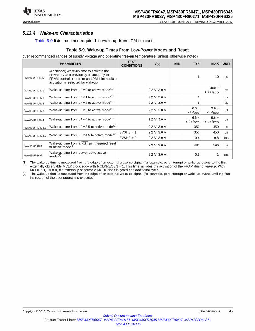
45
MSP430FR6047, MSP430FR60471, MSP430FR6045MSP430FR6037, MSP430FR60371, MSP430FR6035
www.ti.com SLASEB7B –JUNE 2017–REVISED DECEMBER 2017
Submit Documentation FeedbackProduct Folder Links: MSP430FR6047 MSP430FR60471 MSP430FR6045 MSP430FR6037 MSP430FR60371
MSP430FR6035
SpecificationsCopyright © 2017, Texas Instruments Incorporated
5.13.4 Wake-up CharacteristicsTable 5-9 lists the times required to wake up from LPM or reset.
(1) The wake-up time is measured from the edge of an external wake-up signal (for example, port interrupt or wake-up event) to the firstexternally observable MCLK clock edge with MCLKREQEN = 1. This time includes the activation of the FRAM during wakeup. WithMCLKREQEN = 0, the externally observable MCLK clock is gated one additional cycle.
(2) The wake-up time is measured from the edge of an external wake-up signal (for example, port interrupt or wake-up event) until the firstinstruction of the user program is executed.
Table 5-9. Wake-up Times From Low-Power Modes and Resetover recommended ranges of supply voltage and operating free-air temperature (unless otherwise noted)
PARAMETER TESTCONDITIONS VCC MIN TYP MAX UNIT
tWAKE-UP FRAM
(Additional) wake-up time to activate theFRAM in AM if previously disabled by theFRAM controller or from an LPM if immediateactivation is selected for wakeup
6 10 μs
tWAKE-UP LPM0 Wake-up time from LPM0 to active mode (1) 2.2 V, 3.0 V 400 +1.5 / fDCO
ns
tWAKE-UP LPM1 Wake-up time from LPM1 to active mode (1) 2.2 V, 3.0 V 6 μstWAKE-UP LPM2 Wake-up time from LPM2 to active mode (1) 2.2 V, 3.0 V 6 μs
tWAKE-UP LPM3 Wake-up time from LPM3 to active mode (1) 2.2 V, 3.0 V 6.6 +2.0/fDCO
9.6 +2.5/fDCO
μs
tWAKE-UP LPM4 Wake-up time from LPM4 to active mode (1) 2.2 V, 3.0 V 6.6 +2.0 / fDCO
9.6 +2.5 / fDCO
μs
tWAKE-UP LPM3.5 Wake-up time from LPM3.5 to active mode (2) 2.2 V, 3.0 V 350 450 μs
tWAKE-UP LPM4.5 Wake-up time from LPM4.5 to active mode (2) SVSHE = 1 2.2 V, 3.0 V 350 450 μsSVSHE = 0 2.2 V, 3.0 V 0.4 0.8 ms
tWAKE-UP-RSTWake-up time from a RST pin triggered resetto active mode (2) 2.2 V, 3.0 V 480 596 μs
tWAKE-UP-BORWake-up time from power-up to activemode (2) 2.2 V, 3.0 V 0.5 1 ms
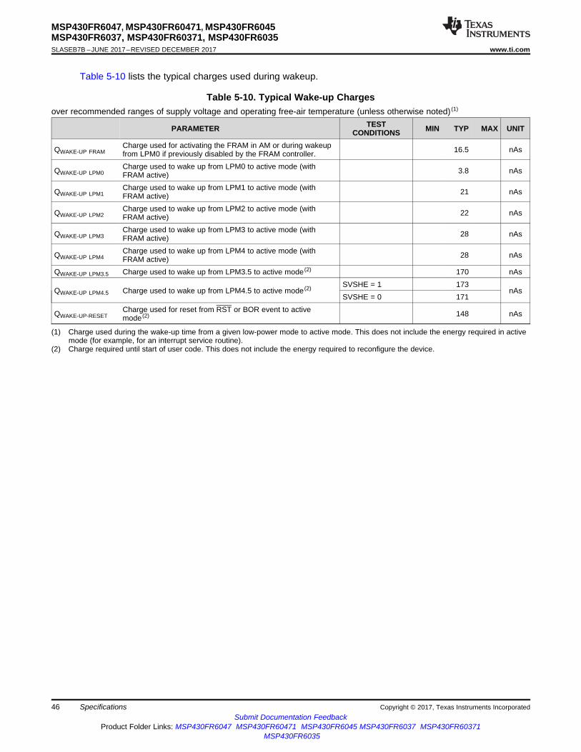
46
MSP430FR6047, MSP430FR60471, MSP430FR6045MSP430FR6037, MSP430FR60371, MSP430FR6035SLASEB7B –JUNE 2017–REVISED DECEMBER 2017 www.ti.com
Submit Documentation FeedbackProduct Folder Links: MSP430FR6047 MSP430FR60471 MSP430FR6045 MSP430FR6037 MSP430FR60371
MSP430FR6035
Specifications Copyright © 2017, Texas Instruments Incorporated
Table 5-10 lists the typical charges used during wakeup.
(1) Charge used during the wake-up time from a given low-power mode to active mode. This does not include the energy required in activemode (for example, for an interrupt service routine).
(2) Charge required until start of user code. This does not include the energy required to reconfigure the device.
Table 5-10. Typical Wake-up Chargesover recommended ranges of supply voltage and operating free-air temperature (unless otherwise noted) (1)
PARAMETER TESTCONDITIONS MIN TYP MAX UNIT
QWAKE-UP FRAMCharge used for activating the FRAM in AM or during wakeupfrom LPM0 if previously disabled by the FRAM controller. 16.5 nAs
QWAKE-UP LPM0Charge used to wake up from LPM0 to active mode (withFRAM active) 3.8 nAs
QWAKE-UP LPM1Charge used to wake up from LPM1 to active mode (withFRAM active) 21 nAs
QWAKE-UP LPM2Charge used to wake up from LPM2 to active mode (withFRAM active) 22 nAs
QWAKE-UP LPM3Charge used to wake up from LPM3 to active mode (withFRAM active) 28 nAs
QWAKE-UP LPM4Charge used to wake up from LPM4 to active mode (withFRAM active) 28 nAs
QWAKE-UP LPM3.5 Charge used to wake up from LPM3.5 to active mode (2) 170 nAs
QWAKE-UP LPM4.5 Charge used to wake up from LPM4.5 to active mode (2) SVSHE = 1 173nAs
SVSHE = 0 171
QWAKE-UP-RESETCharge used for reset from RST or BOR event to activemode (2) 148 nAs
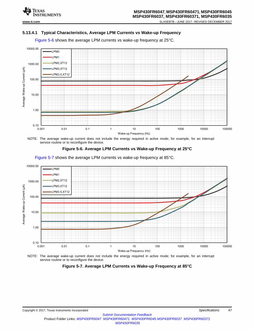
0.10
1.00
10.00
100.00
1000.00
10000.00
0.001 0.01 0.1 1 10 100 1000 10000 100000
Avera
ge
Wake-u
pC
urr
ent (µ
A)
Wake-up Frequency (Hz)
LPM0
LPM1
LPM2,XT12
LPM3,XT12
LPM3.5,XT12
0.10
1.00
10.00
100.00
1000.00
10000.00
0.001 0.01 0.1 1 10 100 1000 10000 100000
Avera
ge
Wake-u
pC
urr
ent (µ
A)
Wake-up Frequency (Hz)
LPM0
LPM1
LPM2,XT12
LPM3,XT12
LPM3.5,XT12
47
MSP430FR6047, MSP430FR60471, MSP430FR6045MSP430FR6037, MSP430FR60371, MSP430FR6035
www.ti.com SLASEB7B –JUNE 2017–REVISED DECEMBER 2017
Submit Documentation FeedbackProduct Folder Links: MSP430FR6047 MSP430FR60471 MSP430FR6045 MSP430FR6037 MSP430FR60371
MSP430FR6035
SpecificationsCopyright © 2017, Texas Instruments Incorporated
5.13.4.1 Typical Characteristics, Average LPM Currents vs Wake-up Frequency
Figure 5-6 shows the average LPM currents vs wake-up frequency at 25°C.
NOTE: The average wake-up current does not include the energy required in active mode; for example, for an interruptservice routine or to reconfigure the device.
Figure 5-6. Average LPM Currents vs Wake-up Frequency at 25°C
Figure 5-7 shows the average LPM currents vs wake-up frequency at 85°C.
NOTE: The average wake-up current does not include the energy required in active mode; for example, for an interruptservice routine or to reconfigure the device.
Figure 5-7. Average LPM Currents vs Wake-up Frequency at 85°C

48
MSP430FR6047, MSP430FR60471, MSP430FR6045MSP430FR6037, MSP430FR60371, MSP430FR6035SLASEB7B –JUNE 2017–REVISED DECEMBER 2017 www.ti.com
Submit Documentation FeedbackProduct Folder Links: MSP430FR6047 MSP430FR60471 MSP430FR6045 MSP430FR6037 MSP430FR60371
MSP430FR6035
Specifications Copyright © 2017, Texas Instruments Incorporated
5.13.5 Digital I/OsTable 5-11 lists the characteristics of the digital inputs.
(1) If the port pins PJ.4/LFXIN and PJ.5/LFXOUT are used as digital I/Os, they are connected by a 4-pF capacitor and a 35-MΩ resistor inseries. At frequencies of approximately 1 kHz and lower, the 4-pF capacitor can add to the pin capacitance of PJ.4/LFXIN and/orPJ.5/LFXOUT.
(2) The input leakage current is measured with VSS or VCC applied to the corresponding pins, unless otherwise noted.(3) The input leakage of the digital port pins is measured individually. The port pin is selected for input and the pullup or pulldown resistor is
disabled.(4) An external signal sets the interrupt flag every time the minimum interrupt pulse duration t(int) is met. It might be set by trigger signals
shorter than t(int).(5) Not applicable if RST/NMI pin configured as NMI
Table 5-11. Digital Inputsover recommended ranges of supply voltage and operating free-air temperature (unless otherwise noted)
PARAMETER TEST CONDITIONS VCC MIN TYP MAX UNIT
VIT+ Positive-going input threshold voltage2.2 V 1.2 1.65
V3.0 V 1.65 2.25
VIT– Negative-going input threshold voltage2.2 V 0.55 1.00
V3.0 V 0.75 1.35
Vhys Input voltage hysteresis (VIT+ – VIT–)2.2 V 0.44 0.98
V3.0 V 0.60 1.30
RPull Pullup or pulldown resistor For pullup: VIN = VSSFor pulldown: VIN = VCC
20 35 50 kΩ
CI,dig Input capacitance, digital only port pins VIN = VSS or VCC 3 pF
CI,anaInput capacitance, port pins with shared analogfunctions (1) VIN = VSS or VCC 5 pF
Ilkg(Px.y) High-impedance input leakage current See (2) (3) 2.2 V,3.0 V –20 +20 nA
t(int)External interrupt timing (external trigger pulseduration to set interrupt flag) (4)
Ports with interruptcapability (see Section 1.4and Section 4.3).
2.2 V,3.0 V 20 ns
t(RST) External reset pulse duration on RST (5) 2.2 V,3.0 V 2 µs

49
MSP430FR6047, MSP430FR60471, MSP430FR6045MSP430FR6037, MSP430FR60371, MSP430FR6035
www.ti.com SLASEB7B –JUNE 2017–REVISED DECEMBER 2017
Submit Documentation FeedbackProduct Folder Links: MSP430FR6047 MSP430FR60471 MSP430FR6045 MSP430FR6037 MSP430FR60371
MSP430FR6035
SpecificationsCopyright © 2017, Texas Instruments Incorporated
Table 5-12 lists the characteristics of the digital outputs.
(1) The maximum total current, I(OHmax) and I(OLmax), for all outputs combined should not exceed ±48 mA to hold the maximum voltage dropspecified.
(2) The maximum total current, I(OHmax) and I(OLmax), for all outputs combined should not exceed ±100 mA to hold the maximum voltagedrop specified.
(3) The port can output frequencies at least up to the specified limit, and the port might support higher frequencies.(4) A resistive divider with 2 × R1 and R1 = 1.6 kΩ between VCC and VSS is used as load. The output is connected to the center tap of the
divider. CL = 20 pF is connected from the output to VSS.(5) The output voltage reaches at least 10% and 90% VCC at the specified toggle frequency.
Table 5-12. Digital Outputsover recommended ranges of supply voltage and operating free-air temperature (unless otherwise noted)
PARAMETER TEST CONDITIONS VCC MIN TYP MAX UNIT
VOHHigh-level output voltage(see Figure 5-10 and Figure 5-11)
I(OHmax) = –1 mA (1)
2.2 V
VCC –0.25 VCC
VI(OHmax) = –3 mA (2) VCC –
0.60 VCC
I(OHmax) = –2 mA (1)
3.0 V
VCC –0.25 VCC
I(OHmax) = –6 mA (2) VCC –0.60 VCC
VOLLow-level output voltage(see Figure 5-8 and Figure 5-9)
I(OLmax) = 1 mA (1)
2.2 VVSS
VSS +0.25
VI(OLmax) = 3 mA (2) VSS
VSS +0.60
I(OLmax) = 2 mA (1)
3.0 VVSS
VSS +0.25
I(OLmax) = 6 mA (2) VSSVSS +
0.60
fPx.y Port output frequency (with load) (3) CL = 20 pF, RL(4) (5) 2.2 V 16
MHz3.0 V 16
fPort_CLK Clock output frequency (3)ACLK, MCLK, or SMCLK atconfigured output port,CL = 20 pF (5)
2.2 V 16MHz
3.0 V 16
trise,dig Port output rise time, digital only port pins CL = 20 pF2.2 V 4 15
ns3.0 V 3 15
tfall,dig Port output fall time, digital only port pins CL = 20 pF2.2 V 4 15
ns3.0 V 3 15
trise,anaPort output rise time, port pins with sharedanalog functions CL = 20 pF
2.2 V 6 15ns
3.0 V 4 15
tfall,anaPort output fall time, port pins with sharedanalog functions CL = 20 pF
2.2 V 6 15ns
3.0 V 4 15

-15
-10
-5
0
0 0.5 1 1.5 2
Hig
h-L
eve
lO
utp
ut
Cu
rre
nt
(mA
)
High-Level Output Voltage (V)
25°C
85°C
C001
P1.1-30
-20
-10
0
0 0.5 1 1.5 2 2.5 3
Hig
h-L
eve
lO
utp
ut
Cu
rre
nt
(mA
)
High-Level Output Voltage (V)
25°C
85°C
C001
P1.1
0
5
10
15
0 0.5 1 1.5 2
Low
-Level
Outp
ut
Curr
ent
(mA
)
Low-Level Output Voltage (V)
25°C
85°C
C001
P1.10
10
20
30
0 0.5 1 1.5 2 2.5 3
Low
-Level
Outp
ut
Curr
ent
(mA
)
Low-Level Output Voltage (V)
25°C
85°C
C001
P1.1
50
MSP430FR6047, MSP430FR60471, MSP430FR6045MSP430FR6037, MSP430FR60371, MSP430FR6035SLASEB7B –JUNE 2017–REVISED DECEMBER 2017 www.ti.com
Submit Documentation FeedbackProduct Folder Links: MSP430FR6047 MSP430FR60471 MSP430FR6045 MSP430FR6037 MSP430FR60371
MSP430FR6035
Specifications Copyright © 2017, Texas Instruments Incorporated
5.13.5.1 Typical Characteristics, Digital Outputs
VCC = 2.2 V
Figure 5-8. Typical Low-Level Output Current vsLow-Level Output Voltage
VCC = 3.0 V
Figure 5-9. Typical Low-Level Output Current vsLow-Level Output Voltage
VCC = 2.2 V
Figure 5-10. Typical High-Level Output Current vsHigh-Level Output Voltage
VCC = 3.0 V
Figure 5-11. Typical High-Level Output Current vsHigh-Level Output Voltage

51
MSP430FR6047, MSP430FR60471, MSP430FR6045MSP430FR6037, MSP430FR60371, MSP430FR6035
www.ti.com SLASEB7B –JUNE 2017–REVISED DECEMBER 2017
Submit Documentation FeedbackProduct Folder Links: MSP430FR6047 MSP430FR60471 MSP430FR6045 MSP430FR6037 MSP430FR60371
MSP430FR6035
SpecificationsCopyright © 2017, Texas Instruments Incorporated
5.13.6 LEATable 5-13 lists the characteristics of the LEA.
Table 5-13. Low-Energy Accelerator (LEA) Performanceover recommended ranges of supply voltage and operating free-air temperature (unless otherwise noted)
PARAMETER TEST CONDITIONS MIN TYP MAX UNIT
fLEAFrequency for specifiedperformance MCLK 16 MHz
W_LEA_FFT LEA subsystem energy on fastFourier transform
Complex FFT 128 pt. Q.15 withrandom data in LEA-RAM
VCORE = 3 V,MCLK = 16 MHz 350 nJ
W_LEA_FIR LEA subsystem energy on finiteimpulse response
Real FIR on random Q.31 data with128 taps on 24 points
VCORE = 3 V,MCLK = 16 MHz 2.6 µJ
W_LEA_ADD LEA subsystem energy onadditions
On 32 Q.31 elements with randomvalue out of LEA-RAM with linearaddress increment
VCORE = 3 V,MCLK = 16 MHz 6.6 nJ
5.13.7 Timer_A and Timer_BTable 5-14 lists the characteristics of Timer_A.
Table 5-14. Timer_Aover recommended ranges of supply voltage and operating free-air temperature (unless otherwise noted)
PARAMETER TEST CONDITIONS VCC MIN TYP MAX UNIT
fTA Timer_A input clock frequencyInternal: SMCLK or ACLK,External: TACLK,Duty cycle = 50% ±10%
2.2 V, 3.0 V 16 MHz
tTA,cap Timer_A capture timing All capture inputs, minimum pulseduration required for capture 2.2 V, 3.0 V 20 ns
Table 5-15 lists the characteristics of Timer_B.
Table 5-15. Timer_Bover recommended ranges of supply voltage and operating free-air temperature (unless otherwise noted)
PARAMETER TEST CONDITIONS VCC MIN TYP MAX UNIT
fTB Timer_B input clock frequencyInternal: SMCLK or ACLK,External: TBCLK,Duty cycle = 50% ±10%
2.2 V, 3.0 V 16 MHz
tTB,cap Timer_B capture timing All capture inputs, minimum pulseduration required for capture 2.2 V, 3.0 V 20 ns
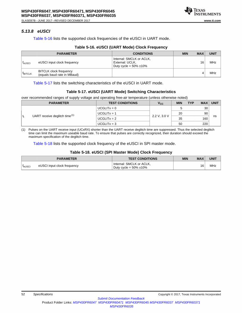
52
MSP430FR6047, MSP430FR60471, MSP430FR6045MSP430FR6037, MSP430FR60371, MSP430FR6035SLASEB7B –JUNE 2017–REVISED DECEMBER 2017 www.ti.com
Submit Documentation FeedbackProduct Folder Links: MSP430FR6047 MSP430FR60471 MSP430FR6045 MSP430FR6037 MSP430FR60371
MSP430FR6035
Specifications Copyright © 2017, Texas Instruments Incorporated
5.13.8 eUSCITable 5-16 lists the supported clock frequencies of the eUSCI in UART mode.
Table 5-16. eUSCI (UART Mode) Clock FrequencyPARAMETER CONDITIONS MIN MAX UNIT
feUSCI eUSCI input clock frequencyInternal: SMCLK or ACLK,External: UCLK,Duty cycle = 50% ±10%
16 MHz
fBITCLKBITCLK clock frequency(equals baud rate in MBaud) 4 MHz
Table 5-17 lists the switching characteristics of the eUSCI in UART mode.
(1) Pulses on the UART receive input (UCxRX) shorter than the UART receive deglitch time are suppressed. Thus the selected deglitchtime can limit the maximum useable baud rate. To ensure that pulses are correctly recognized, their duration should exceed themaximum specification of the deglitch time.
Table 5-17. eUSCI (UART Mode) Switching Characteristicsover recommended ranges of supply voltage and operating free-air temperature (unless otherwise noted)
PARAMETER TEST CONDITIONS VCC MIN TYP MAX UNIT
tt UART receive deglitch time (1)
UCGLITx = 0
2.2 V, 3.0 V
5 30
nsUCGLITx = 1 20 90UCGLITx = 2 35 160UCGLITx = 3 50 220
Table 5-18 lists the supported clock frequency of the eUSCI in SPI master mode.
Table 5-18. eUSCI (SPI Master Mode) Clock FrequencyPARAMETER TEST CONDITIONS MIN MAX UNIT
feUSCI eUSCI input clock frequency Internal: SMCLK or ACLK,Duty cycle = 50% ±10% 16 MHz
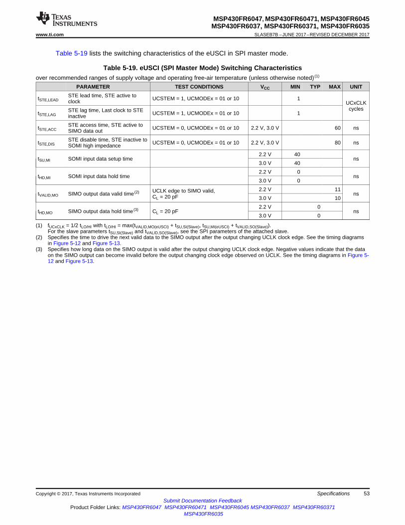
53
MSP430FR6047, MSP430FR60471, MSP430FR6045MSP430FR6037, MSP430FR60371, MSP430FR6035
www.ti.com SLASEB7B –JUNE 2017–REVISED DECEMBER 2017
Submit Documentation FeedbackProduct Folder Links: MSP430FR6047 MSP430FR60471 MSP430FR6045 MSP430FR6037 MSP430FR60371
MSP430FR6035
SpecificationsCopyright © 2017, Texas Instruments Incorporated
Table 5-19 lists the switching characteristics of the eUSCI in SPI master mode.
(1) fUCxCLK = 1/2 tLO/HI with tLO/HI = max(tVALID,MO(eUSCI) + tSU,SI(Slave), tSU,MI(eUSCI) + tVALID,SO(Slave)).For the slave parameters tSU,SI(Slave) and tVALID,SO(Slave), see the SPI parameters of the attached slave.
(2) Specifies the time to drive the next valid data to the SIMO output after the output changing UCLK clock edge. See the timing diagramsin Figure 5-12 and Figure 5-13.
(3) Specifies how long data on the SIMO output is valid after the output changing UCLK clock edge. Negative values indicate that the dataon the SIMO output can become invalid before the output changing clock edge observed on UCLK. See the timing diagrams in Figure 5-12 and Figure 5-13.
Table 5-19. eUSCI (SPI Master Mode) Switching Characteristicsover recommended ranges of supply voltage and operating free-air temperature (unless otherwise noted) (1)
PARAMETER TEST CONDITIONS VCC MIN TYP MAX UNIT
tSTE,LEADSTE lead time, STE active toclock UCSTEM = 1, UCMODEx = 01 or 10 1
UCxCLKcycles
tSTE,LAGSTE lag time, Last clock to STEinactive UCSTEM = 1, UCMODEx = 01 or 10 1
tSTE,ACCSTE access time, STE active toSIMO data out UCSTEM = 0, UCMODEx = 01 or 10 2.2 V, 3.0 V 60 ns
tSTE,DISSTE disable time, STE inactive toSOMI high impedance UCSTEM = 0, UCMODEx = 01 or 10 2.2 V, 3.0 V 80 ns
tSU,MI SOMI input data setup time2.2 V 40
ns3.0 V 40
tHD,MI SOMI input data hold time2.2 V 0
ns3.0 V 0
tVALID,MO SIMO output data valid time (2) UCLK edge to SIMO valid,CL = 20 pF
2.2 V 11ns
3.0 V 10
tHD,MO SIMO output data hold time (3) CL = 20 pF2.2 V 0
ns3.0 V 0
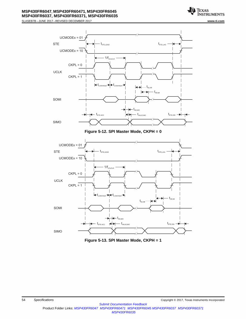
tSU,MI
tHD,MI
UCLK
SOMI
SIMO
tVALID,MO
CKPL = 0
CKPL = 1
tLOW/HIGH tLOW/HIGH
1/fUCxCLK
tSTE,LEAD tSTE,LAG
tSTE,ACC
UCMODEx = 01
UCMODEx = 10
STE
tHD,MO
tSTE,DIS
tSU,MI
tHD,MI
UCLK
SOMI
SIMO
tVALID,MO
CKPL = 0
CKPL = 1
tLOW/HIGH tLOW/HIGH
1/fUCxCLK
STE tSTE,LEAD tSTE,LAG
UCMODEx = 01
UCMODEx = 10
tHD,MO
tSTE,ACC tSTE,DIS
54
MSP430FR6047, MSP430FR60471, MSP430FR6045MSP430FR6037, MSP430FR60371, MSP430FR6035SLASEB7B –JUNE 2017–REVISED DECEMBER 2017 www.ti.com
Submit Documentation FeedbackProduct Folder Links: MSP430FR6047 MSP430FR60471 MSP430FR6045 MSP430FR6037 MSP430FR60371
MSP430FR6035
Specifications Copyright © 2017, Texas Instruments Incorporated
Figure 5-12. SPI Master Mode, CKPH = 0
Figure 5-13. SPI Master Mode, CKPH = 1
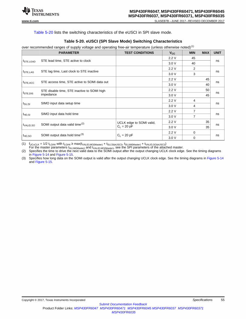
55
MSP430FR6047, MSP430FR60471, MSP430FR6045MSP430FR6037, MSP430FR60371, MSP430FR6035
www.ti.com SLASEB7B –JUNE 2017–REVISED DECEMBER 2017
Submit Documentation FeedbackProduct Folder Links: MSP430FR6047 MSP430FR60471 MSP430FR6045 MSP430FR6037 MSP430FR60371
MSP430FR6035
SpecificationsCopyright © 2017, Texas Instruments Incorporated
Table 5-20 lists the switching characteristics of the eUSCI in SPI slave mode.
(1) fUCxCLK = 1/2 tLO/HI with tLO/HI ≥ max(tVALID,MO(Master) + tSU,SI(eUSCI), tSU,MI(Master) + tVALID,SO(eUSCI))For the master parameters tSU,MI(Master) and tVALID,MO(Master), see the SPI parameters of the attached master.
(2) Specifies the time to drive the next valid data to the SOMI output after the output changing UCLK clock edge. See the timing diagramsin Figure 5-14 and Figure 5-15.
(3) Specifies how long data on the SOMI output is valid after the output changing UCLK clock edge. See the timing diagrams in Figure 5-14and Figure 5-15.
Table 5-20. eUSCI (SPI Slave Mode) Switching Characteristicsover recommended ranges of supply voltage and operating free-air temperature (unless otherwise noted) (1)
PARAMETER TEST CONDITIONS VCC MIN MAX UNIT
tSTE,LEAD STE lead time, STE active to clock2.2 V 45
ns3.0 V 40
tSTE,LAG STE lag time, Last clock to STE inactive2.2 V 2
ns3.0 V 3
tSTE,ACC STE access time, STE active to SOMI data out2.2 V 45
ns3.0 V 40
tSTE,DISSTE disable time, STE inactive to SOMI highimpedance
2.2 V 50ns
3.0 V 45
tSU,SI SIMO input data setup time2.2 V 4
ns3.0 V 4
tHD,SI SIMO input data hold time2.2 V 7
ns3.0 V 7
tVALID,SO SOMI output data valid time (2) UCLK edge to SOMI valid,CL = 20 pF
2.2 V 35ns
3.0 V 35
tHD,SO SOMI output data hold time (3) CL = 20 pF2.2 V 0
ns3.0 V 0
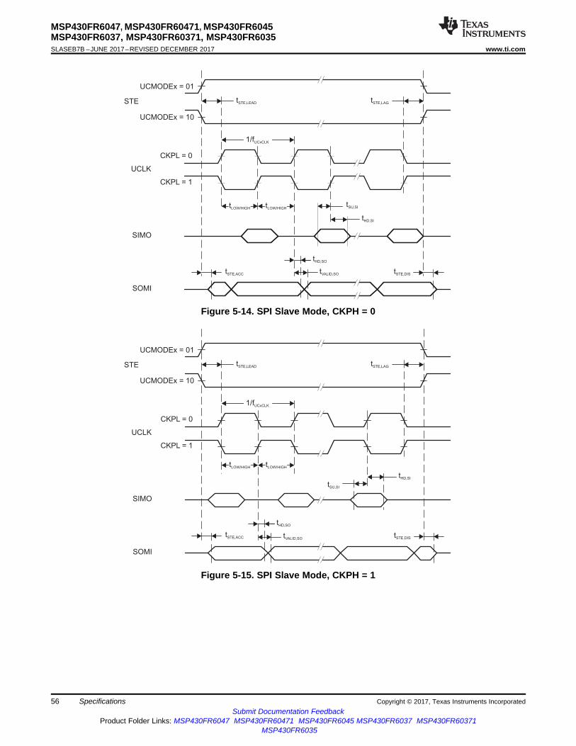
UCLK
CKPL = 0
CKPL = 1
SOMI
SIMO
tSU,SI
tHD,SI
tVALID,SO
tHD,SO
tLOW/HIGH
1/fUCxCLK
tLOW/HIGH
tSTE,DIStSTE,ACC
STE tSTE,LEAD tSTE,LAG
UCMODEx = 01
UCMODEx = 10
UCLK
CKPL = 0
CKPL = 1
SOMI
SIMO
tSU,SI
tHD,SI
tVALID,SO
tLOW/HIGH
1/fUCxCLK
tLOW/HIGH
tSTE,DIStSTE,ACC
STE tSTE,LEAD tSTE,LAG
UCMODEx = 01
UCMODEx = 10
tHD,SO
56
MSP430FR6047, MSP430FR60471, MSP430FR6045MSP430FR6037, MSP430FR60371, MSP430FR6035SLASEB7B –JUNE 2017–REVISED DECEMBER 2017 www.ti.com
Submit Documentation FeedbackProduct Folder Links: MSP430FR6047 MSP430FR60471 MSP430FR6045 MSP430FR6037 MSP430FR60371
MSP430FR6035
Specifications Copyright © 2017, Texas Instruments Incorporated
Figure 5-14. SPI Slave Mode, CKPH = 0
Figure 5-15. SPI Slave Mode, CKPH = 1

SDA
SCL
tHD,DAT
tSU,DAT
tHD,STA
tHIGHtLOW
tBUFtHD,STAtSU,STA
tSP
tSU,STO
57
MSP430FR6047, MSP430FR60471, MSP430FR6045MSP430FR6037, MSP430FR60371, MSP430FR6035
www.ti.com SLASEB7B –JUNE 2017–REVISED DECEMBER 2017
Submit Documentation FeedbackProduct Folder Links: MSP430FR6047 MSP430FR60471 MSP430FR6045 MSP430FR6037 MSP430FR60371
MSP430FR6035
SpecificationsCopyright © 2017, Texas Instruments Incorporated
Table 5-21 lists the switching characteristics of the eUSCI in I2C mode.
Table 5-21. eUSCI (I2C Mode) Switching Characteristicsover recommended ranges of supply voltage and operating free-air temperature (unless otherwise noted) (see Figure 5-16)
PARAMETER TEST CONDITIONS VCC MIN TYP MAX UNIT
feUSCI eUSCI input clock frequencyInternal: SMCLK or ACLK,External: UCLK,Duty cycle = 50% ±10%
16 MHz
fSCL SCL clock frequency 2.2 V, 3.0 V 0 400 kHz
tHD,STA Hold time (repeated) STARTfSCL = 100 kHz
2.2 V, 3.0 V4.0
µsfSCL > 100 kHz 0.6
tSU,STA Setup time for a repeated STARTfSCL = 100 kHz
2.2 V, 3.0 V4.7
µsfSCL > 100 kHz 0.6
tHD,DAT Data hold time 2.2 V, 3.0 V 0 nstSU,DAT Data setup time 2.2 V, 3.0 V 100 ns
tSU,STO Setup time for STOPfSCL = 100 kHz
2.2 V, 3.0 V4.0
µsfSCL > 100 kHz 0.6
tBUFBus free time between a STOP andSTART condition
fSCL = 100 kHz 4.7us
fSCL > 100 kHz 1.3
tSPPulse duration of spikes suppressed byinput filter
UCGLITx = 0
2.2 V, 3.0 V
50 250
nsUCGLITx = 1 25 125UCGLITx = 2 12.5 62.5UCGLITx = 3 6.3 31.5
tTIMEOUT Clock low time-outUCCLTOx = 1
2.2 V, 3.0 V27
msUCCLTOx = 2 30UCCLTOx = 3 33
Figure 5-16. I2C Mode Timing
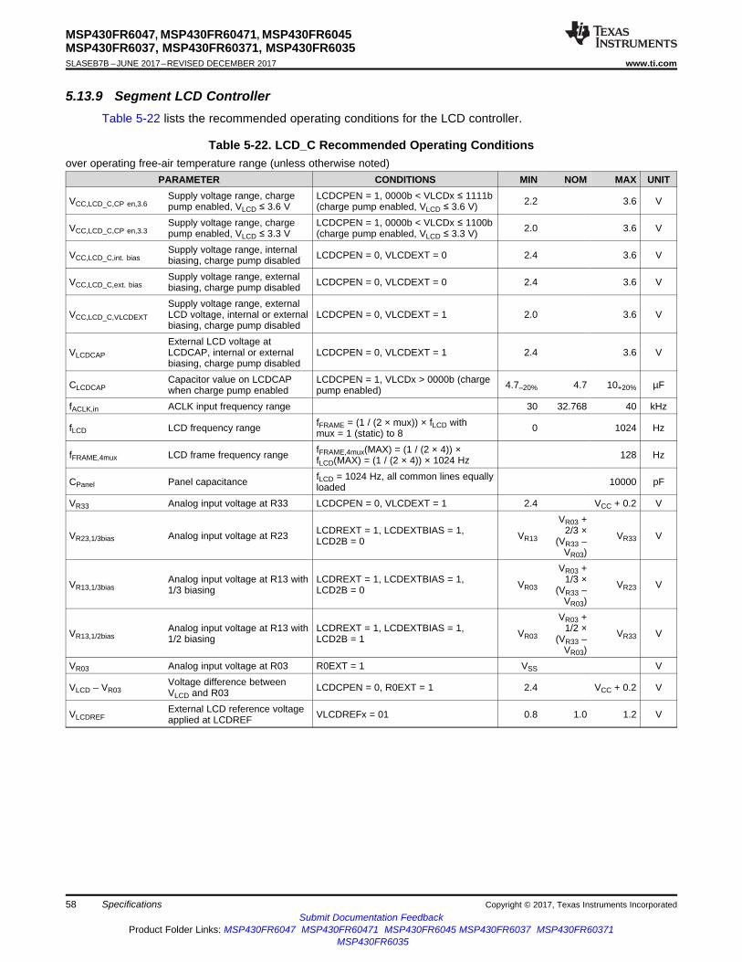
58
MSP430FR6047, MSP430FR60471, MSP430FR6045MSP430FR6037, MSP430FR60371, MSP430FR6035SLASEB7B –JUNE 2017–REVISED DECEMBER 2017 www.ti.com
Submit Documentation FeedbackProduct Folder Links: MSP430FR6047 MSP430FR60471 MSP430FR6045 MSP430FR6037 MSP430FR60371
MSP430FR6035
Specifications Copyright © 2017, Texas Instruments Incorporated
5.13.9 Segment LCD ControllerTable 5-22 lists the recommended operating conditions for the LCD controller.
Table 5-22. LCD_C Recommended Operating Conditionsover operating free-air temperature range (unless otherwise noted)
PARAMETER CONDITIONS MIN NOM MAX UNIT
VCC,LCD_C,CP en,3.6Supply voltage range, chargepump enabled, VLCD ≤ 3.6 V
LCDCPEN = 1, 0000b < VLCDx ≤ 1111b(charge pump enabled, VLCD ≤ 3.6 V) 2.2 3.6 V
VCC,LCD_C,CP en,3.3Supply voltage range, chargepump enabled, VLCD ≤ 3.3 V
LCDCPEN = 1, 0000b < VLCDx ≤ 1100b(charge pump enabled, VLCD ≤ 3.3 V) 2.0 3.6 V
VCC,LCD_C,int. biasSupply voltage range, internalbiasing, charge pump disabled LCDCPEN = 0, VLCDEXT = 0 2.4 3.6 V
VCC,LCD_C,ext. biasSupply voltage range, externalbiasing, charge pump disabled LCDCPEN = 0, VLCDEXT = 0 2.4 3.6 V
VCC,LCD_C,VLCDEXT
Supply voltage range, externalLCD voltage, internal or externalbiasing, charge pump disabled
LCDCPEN = 0, VLCDEXT = 1 2.0 3.6 V
VLCDCAP
External LCD voltage atLCDCAP, internal or externalbiasing, charge pump disabled
LCDCPEN = 0, VLCDEXT = 1 2.4 3.6 V
CLCDCAPCapacitor value on LCDCAPwhen charge pump enabled
LCDCPEN = 1, VLCDx > 0000b (chargepump enabled) 4.7–20% 4.7 10+20% µF
fACLK,in ACLK input frequency range 30 32.768 40 kHz
fLCD LCD frequency range fFRAME = (1 / (2 × mux)) × fLCD withmux = 1 (static) to 8 0 1024 Hz
fFRAME,4mux LCD frame frequency range fFRAME,4mux(MAX) = (1 / (2 × 4)) ×fLCD(MAX) = (1 / (2 × 4)) × 1024 Hz 128 Hz
CPanel Panel capacitance fLCD = 1024 Hz, all common lines equallyloaded 10000 pF
VR33 Analog input voltage at R33 LCDCPEN = 0, VLCDEXT = 1 2.4 VCC + 0.2 V
VR23,1/3bias Analog input voltage at R23 LCDREXT = 1, LCDEXTBIAS = 1,LCD2B = 0 VR13
VR03 +2/3 ×
(VR33 –VR03)
VR33 V
VR13,1/3biasAnalog input voltage at R13 with1/3 biasing
LCDREXT = 1, LCDEXTBIAS = 1,LCD2B = 0 VR03
VR03 +1/3 ×
(VR33 –VR03)
VR23 V
VR13,1/2biasAnalog input voltage at R13 with1/2 biasing
LCDREXT = 1, LCDEXTBIAS = 1,LCD2B = 1 VR03
VR03 +1/2 ×
(VR33 –VR03)
VR33 V
VR03 Analog input voltage at R03 R0EXT = 1 VSS V
VLCD – VR03Voltage difference betweenVLCD and R03 LCDCPEN = 0, R0EXT = 1 2.4 VCC + 0.2 V
VLCDREFExternal LCD reference voltageapplied at LCDREF VLCDREFx = 01 0.8 1.0 1.2 V
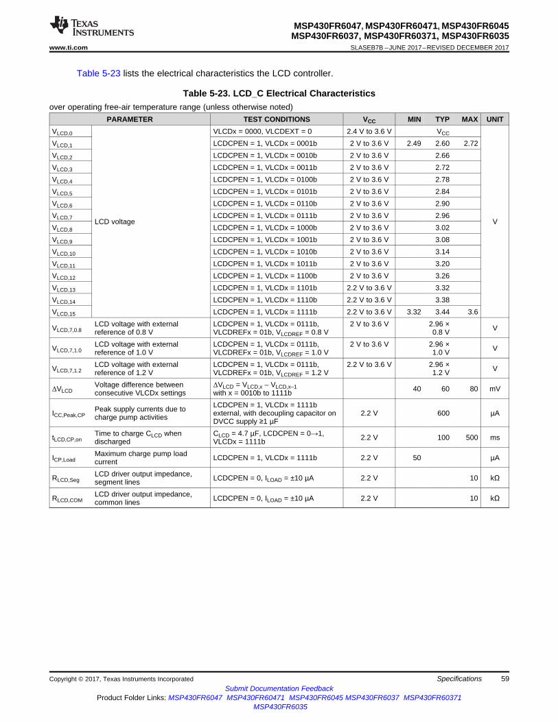
59
MSP430FR6047, MSP430FR60471, MSP430FR6045MSP430FR6037, MSP430FR60371, MSP430FR6035
www.ti.com SLASEB7B –JUNE 2017–REVISED DECEMBER 2017
Submit Documentation FeedbackProduct Folder Links: MSP430FR6047 MSP430FR60471 MSP430FR6045 MSP430FR6037 MSP430FR60371
MSP430FR6035
SpecificationsCopyright © 2017, Texas Instruments Incorporated
Table 5-23 lists the electrical characteristics the LCD controller.
Table 5-23. LCD_C Electrical Characteristicsover operating free-air temperature range (unless otherwise noted)
PARAMETER TEST CONDITIONS VCC MIN TYP MAX UNITVLCD,0
LCD voltage
VLCDx = 0000, VLCDEXT = 0 2.4 V to 3.6 V VCC
V
VLCD,1 LCDCPEN = 1, VLCDx = 0001b 2 V to 3.6 V 2.49 2.60 2.72VLCD,2 LCDCPEN = 1, VLCDx = 0010b 2 V to 3.6 V 2.66VLCD,3 LCDCPEN = 1, VLCDx = 0011b 2 V to 3.6 V 2.72VLCD,4 LCDCPEN = 1, VLCDx = 0100b 2 V to 3.6 V 2.78VLCD,5 LCDCPEN = 1, VLCDx = 0101b 2 V to 3.6 V 2.84VLCD,6 LCDCPEN = 1, VLCDx = 0110b 2 V to 3.6 V 2.90VLCD,7 LCDCPEN = 1, VLCDx = 0111b 2 V to 3.6 V 2.96VLCD,8 LCDCPEN = 1, VLCDx = 1000b 2 V to 3.6 V 3.02VLCD,9 LCDCPEN = 1, VLCDx = 1001b 2 V to 3.6 V 3.08VLCD,10 LCDCPEN = 1, VLCDx = 1010b 2 V to 3.6 V 3.14VLCD,11 LCDCPEN = 1, VLCDx = 1011b 2 V to 3.6 V 3.20VLCD,12 LCDCPEN = 1, VLCDx = 1100b 2 V to 3.6 V 3.26VLCD,13 LCDCPEN = 1, VLCDx = 1101b 2.2 V to 3.6 V 3.32VLCD,14 LCDCPEN = 1, VLCDx = 1110b 2.2 V to 3.6 V 3.38VLCD,15 LCDCPEN = 1, VLCDx = 1111b 2.2 V to 3.6 V 3.32 3.44 3.6
VLCD,7,0.8LCD voltage with externalreference of 0.8 V
LCDCPEN = 1, VLCDx = 0111b,VLCDREFx = 01b, VLCDREF = 0.8 V
2 V to 3.6 V 2.96 ×0.8 V V
VLCD,7,1.0LCD voltage with externalreference of 1.0 V
LCDCPEN = 1, VLCDx = 0111b,VLCDREFx = 01b, VLCDREF = 1.0 V
2 V to 3.6 V 2.96 ×1.0 V V
VLCD,7,1.2LCD voltage with externalreference of 1.2 V
LCDCPEN = 1, VLCDx = 0111b,VLCDREFx = 01b, VLCDREF = 1.2 V
2.2 V to 3.6 V 2.96 ×1.2 V V
ΔVLCDVoltage difference betweenconsecutive VLCDx settings
ΔVLCD = VLCD,x – VLCD,x–1with x = 0010b to 1111b 40 60 80 mV
ICC,Peak,CPPeak supply currents due tocharge pump activities
LCDCPEN = 1, VLCDx = 1111bexternal, with decoupling capacitor onDVCC supply ≥1 µF
2.2 V 600 µA
tLCD,CP,onTime to charge CLCD whendischarged
CLCD = 4.7 µF, LCDCPEN = 0→1,VLCDx = 1111b 2.2 V 100 500 ms
ICP,LoadMaximum charge pump loadcurrent LCDCPEN = 1, VLCDx = 1111b 2.2 V 50 µA
RLCD,SegLCD driver output impedance,segment lines LCDCPEN = 0, ILOAD = ±10 µA 2.2 V 10 kΩ
RLCD,COMLCD driver output impedance,common lines LCDCPEN = 0, ILOAD = ±10 µA 2.2 V 10 kΩ
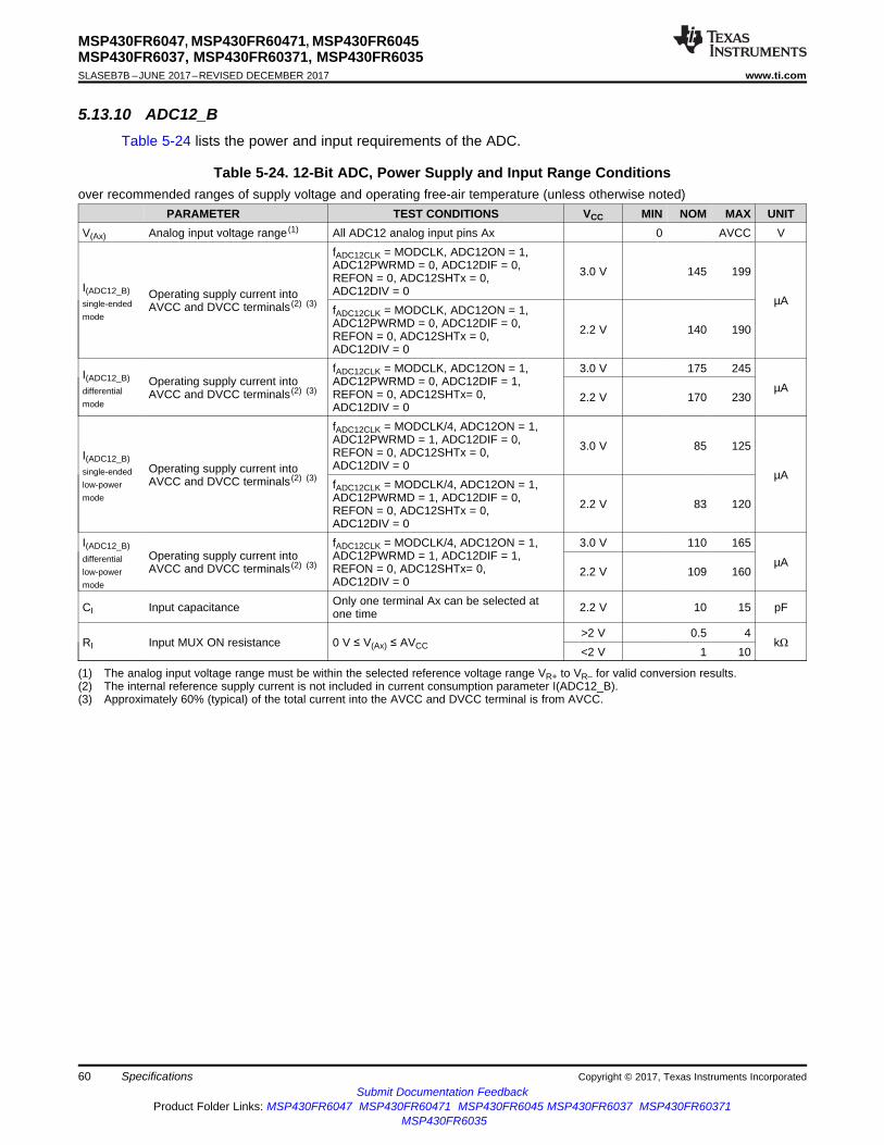
60
MSP430FR6047, MSP430FR60471, MSP430FR6045MSP430FR6037, MSP430FR60371, MSP430FR6035SLASEB7B –JUNE 2017–REVISED DECEMBER 2017 www.ti.com
Submit Documentation FeedbackProduct Folder Links: MSP430FR6047 MSP430FR60471 MSP430FR6045 MSP430FR6037 MSP430FR60371
MSP430FR6035
Specifications Copyright © 2017, Texas Instruments Incorporated
5.13.10 ADC12_BTable 5-24 lists the power and input requirements of the ADC.
(1) The analog input voltage range must be within the selected reference voltage range VR+ to VR– for valid conversion results.(2) The internal reference supply current is not included in current consumption parameter I(ADC12_B).(3) Approximately 60% (typical) of the total current into the AVCC and DVCC terminal is from AVCC.
Table 5-24. 12-Bit ADC, Power Supply and Input Range Conditionsover recommended ranges of supply voltage and operating free-air temperature (unless otherwise noted)
PARAMETER TEST CONDITIONS VCC MIN NOM MAX UNITV(Ax) Analog input voltage range (1) All ADC12 analog input pins Ax 0 AVCC V
I(ADC12_B)single-endedmode
Operating supply current intoAVCC and DVCC terminals (2) (3)
fADC12CLK = MODCLK, ADC12ON = 1,ADC12PWRMD = 0, ADC12DIF = 0,REFON = 0, ADC12SHTx = 0,ADC12DIV = 0
3.0 V 145 199
µAfADC12CLK = MODCLK, ADC12ON = 1,ADC12PWRMD = 0, ADC12DIF = 0,REFON = 0, ADC12SHTx = 0,ADC12DIV = 0
2.2 V 140 190
I(ADC12_B)differentialmode
Operating supply current intoAVCC and DVCC terminals (2) (3)
fADC12CLK = MODCLK, ADC12ON = 1,ADC12PWRMD = 0, ADC12DIF = 1,REFON = 0, ADC12SHTx= 0,ADC12DIV = 0
3.0 V 175 245
µA2.2 V 170 230
I(ADC12_B)single-endedlow-powermode
Operating supply current intoAVCC and DVCC terminals (2) (3)
fADC12CLK = MODCLK/4, ADC12ON = 1,ADC12PWRMD = 1, ADC12DIF = 0,REFON = 0, ADC12SHTx = 0,ADC12DIV = 0
3.0 V 85 125
µAfADC12CLK = MODCLK/4, ADC12ON = 1,ADC12PWRMD = 1, ADC12DIF = 0,REFON = 0, ADC12SHTx = 0,ADC12DIV = 0
2.2 V 83 120
I(ADC12_B)differentiallow-powermode
Operating supply current intoAVCC and DVCC terminals (2) (3)
fADC12CLK = MODCLK/4, ADC12ON = 1,ADC12PWRMD = 1, ADC12DIF = 1,REFON = 0, ADC12SHTx= 0,ADC12DIV = 0
3.0 V 110 165
µA2.2 V 109 160
CI Input capacitance Only one terminal Ax can be selected atone time 2.2 V 10 15 pF
RI Input MUX ON resistance 0 V ≤ V(Ax) ≤ AVCC>2 V 0.5 4
kΩ<2 V 1 10
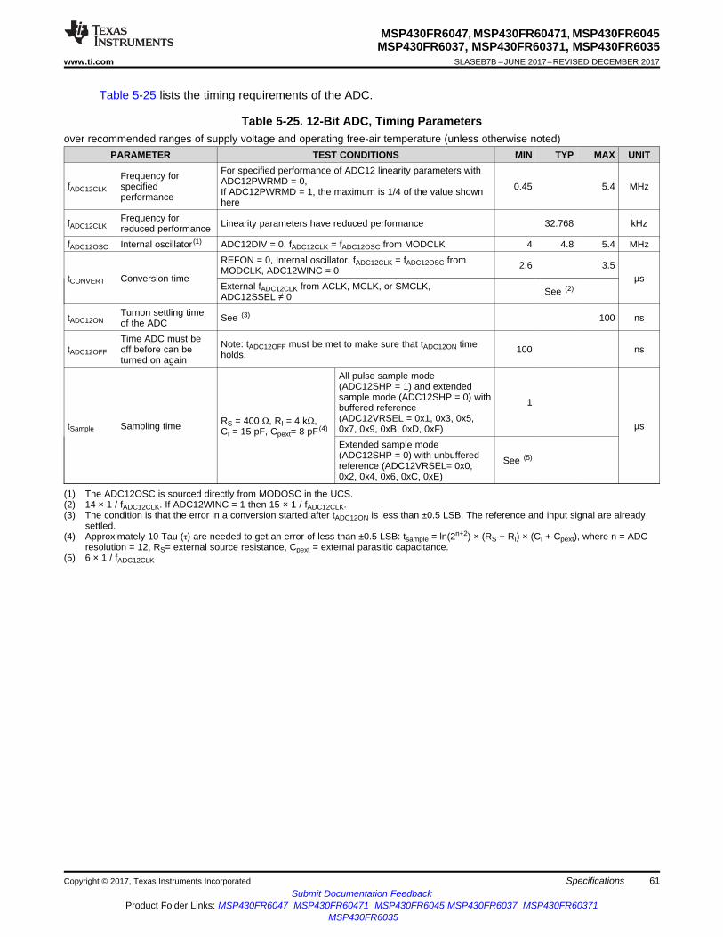
61
MSP430FR6047, MSP430FR60471, MSP430FR6045MSP430FR6037, MSP430FR60371, MSP430FR6035
www.ti.com SLASEB7B –JUNE 2017–REVISED DECEMBER 2017
Submit Documentation FeedbackProduct Folder Links: MSP430FR6047 MSP430FR60471 MSP430FR6045 MSP430FR6037 MSP430FR60371
MSP430FR6035
SpecificationsCopyright © 2017, Texas Instruments Incorporated
Table 5-25 lists the timing requirements of the ADC.
(1) The ADC12OSC is sourced directly from MODOSC in the UCS.(2) 14 × 1 / fADC12CLK. If ADC12WINC = 1 then 15 × 1 / fADC12CLK.(3) The condition is that the error in a conversion started after tADC12ON is less than ±0.5 LSB. The reference and input signal are already
settled.(4) Approximately 10 Tau (τ) are needed to get an error of less than ±0.5 LSB: tsample = ln(2n+2) × (RS + RI) × (CI + Cpext), where n = ADC
resolution = 12, RS= external source resistance, Cpext = external parasitic capacitance.(5) 6 × 1 / fADC12CLK
Table 5-25. 12-Bit ADC, Timing Parametersover recommended ranges of supply voltage and operating free-air temperature (unless otherwise noted)
PARAMETER TEST CONDITIONS MIN TYP MAX UNIT
fADC12CLK
Frequency forspecifiedperformance
For specified performance of ADC12 linearity parameters withADC12PWRMD = 0,If ADC12PWRMD = 1, the maximum is 1/4 of the value shownhere
0.45 5.4 MHz
fADC12CLKFrequency forreduced performance Linearity parameters have reduced performance 32.768 kHz
fADC12OSC Internal oscillator (1) ADC12DIV = 0, fADC12CLK = fADC12OSC from MODCLK 4 4.8 5.4 MHz
tCONVERT Conversion time
REFON = 0, Internal oscillator, fADC12CLK = fADC12OSC fromMODCLK, ADC12WINC = 0 2.6 3.5
µsExternal fADC12CLK from ACLK, MCLK, or SMCLK,ADC12SSEL ≠ 0 See (2)
tADC12ONTurnon settling timeof the ADC See (3) 100 ns
tADC12OFF
Time ADC must beoff before can beturned on again
Note: tADC12OFF must be met to make sure that tADC12ON timeholds. 100 ns
tSample Sampling time RS = 400 Ω, RI = 4 kΩ,CI = 15 pF, Cpext= 8 pF (4)
All pulse sample mode(ADC12SHP = 1) and extendedsample mode (ADC12SHP = 0) withbuffered reference(ADC12VRSEL = 0x1, 0x3, 0x5,0x7, 0x9, 0xB, 0xD, 0xF)
1
µs
Extended sample mode(ADC12SHP = 0) with unbufferedreference (ADC12VRSEL= 0x0,0x2, 0x4, 0x6, 0xC, 0xE)
See (5)

62
MSP430FR6047, MSP430FR60471, MSP430FR6045MSP430FR6037, MSP430FR60371, MSP430FR6035SLASEB7B –JUNE 2017–REVISED DECEMBER 2017 www.ti.com
Submit Documentation FeedbackProduct Folder Links: MSP430FR6047 MSP430FR60471 MSP430FR6045 MSP430FR6037 MSP430FR60371
MSP430FR6035
Specifications Copyright © 2017, Texas Instruments Incorporated
Table 5-26 lists the linearity parameters of the ADC.
(1) Offset is measured as the input voltage (at which ADC output transitions from 0 to 1) minus 0.5 LSB.(2) Offset increases as IR drop increases when VR– is AVSS.(3) For details, see the Device Descriptor Table section in the MSP430FR58xx, MSP430FR59xx, and MSP430FR6xx Family User's Guide.
Table 5-26. 12-Bit ADC, Linearity Parametersover recommended ranges of supply voltage and operating free-air temperature (unless otherwise noted)
PARAMETER TEST CONDITIONS MIN TYP MAX UNIT
EI
Integral linearity error (INL) fordifferential input
With external voltage reference (ADC12VRSEL = 0x2,0x3, 0x4, 0x14, 0x15),1.2 V ≤ (VR+ – VR–) ≤ AVCC
±1.8
LSBIntegral linearity error (INL) forsingle-ended inputs
With external voltage reference (ADC12VRSEL = 0x2,0x3, 0x4, 0x14, 0x15),1.2 V ≤ (VR+ – VR–) ≤ AVCC
±2.2
ED Differential linearity error (DNL) With external voltage reference (ADC12VRSEL = 0x2,0x3, 0x4, 0x14, 0x15), –0.99 +1.0 LSB
EO Offset error (1) (2)ADC12VRSEL = 0x1 without TLV calibration,TLV calibration data can be used to improve theparameter (3)
±0.5 ±1.5 mV
EG Gain error
With internal voltage reference VREF = 2.5 V(ADC12VRSEL = 0x1, 0x7, 0x9, 0xB, or 0xD) ±0.2% ±1.7%
With internal voltage reference VREF = 1.2 V(ADC12VRSEL = 0x1, 0x7, 0x9, 0xB, or 0xD) ±0.2% ±2.5%
With external voltage reference without internal buffer(ADC12VRSEL = 0x2 or 0x4) without TLV calibration,VR+ = 2.5 V, VR– = AVSS
±1 ±3LSB
With external voltage reference with internal buffer(ADC12VRSEL = 0x3), VR+ = 2.5 V, VR– = AVSS ±2 ±27
ET Total unadjusted error
With internal voltage reference VREF = 2.5 V(ADC12VRSEL = 0x1, 0x7, 0x9, 0xB, or 0xD) ±0.2% ±1.8%
With internal voltage reference VREF = 1.2 V(ADC12VRSEL = 0x1, 0x7, 0x9, 0xB, or 0xD) ±0.2% ±2.6%
With external voltage reference without internal buffer(ADC12VRSEL = 0x2 or 0x4) without TLV calibration,VR+ = 2.5 V, VR– = AVSS
±1 ±5LSB
With external voltage reference with internal buffer(ADC12VRSEL = 0x3), VR+ = 2.5 V, VR– = AVSS ±1 ±28

63
MSP430FR6047, MSP430FR60471, MSP430FR6045MSP430FR6037, MSP430FR60371, MSP430FR6035
www.ti.com SLASEB7B –JUNE 2017–REVISED DECEMBER 2017
Submit Documentation FeedbackProduct Folder Links: MSP430FR6047 MSP430FR60471 MSP430FR6045 MSP430FR6037 MSP430FR60371
MSP430FR6035
SpecificationsCopyright © 2017, Texas Instruments Incorporated
Table 5-27 lists the dynamic performance characteristics of the ADC with an external reference.
(1) ENOB = (SINAD – 1.76) / 6.02
Table 5-27. 12-Bit ADC, Dynamic Performance With External Referenceover recommended ranges of supply voltage and operating free-air temperature (unless otherwise noted)
PARAMETER TEST CONDITIONS MIN TYP MAX UNITResolution Number of no missing code output-code bits 12 bits
SNRSignal-to-noise with differential inputs VR+ = 2.5 V, VR– = AVSS 71
dBSignal-to-noise with single-ended inputs VR+ = 2.5 V, VR– = AVSS 70
ENOB
Effective number of bits with differential inputs (1) VR+ = 2.5 V, VR– = AVSS 11.4
bitsEffective number of bits with single-ended inputs (1) VR+ = 2.5 V, VR– = AVSS 11.1
Effective number of bits with 32.768-kHz clock(reduced performance) (1)
Reduced performance with fADC12CLKfrom ACLK LFXT 32.768 kHz,VR+ = 2.5 V, VR– = AVSS
10.9
Table 5-28 lists the dynamic performance characteristics of the ADC with an internal reference.
(1) ENOB = (SINAD – 1.76) / 6.02
Table 5-28. 12-Bit ADC, Dynamic Performance With Internal Referenceover recommended ranges of supply voltage and operating free-air temperature (unless otherwise noted)
PARAMETER TEST CONDITIONS MIN TYP MAX UNITResolution Number of no missing code output-code bits 12 bits
SNRSignal-to-noise with differential inputs VR+ = 2.5 V, VR– = AVSS 70
dBSignal-to-noise with single-ended inputs VR+ = 2.5 V, VR– = AVSS 69
ENOB
Effective number of bits with differential inputs (1) VR+ = 2.5 V, VR– = AVSS 11.4
bitsEffective number of bits with single-ended inputs (1) VR+ = 2.5 V, VR– = AVSS 11.0
Effective number of bits with 32.768-kHz clock(reduced performance) (1)
Reduced performance with fADC12CLKfrom ACLK LFXT 32.768 kHz,VR+ = 2.5 V, VR– = AVSS
10.9
Table 5-29 lists the characteristics of the temperature sensor and the V1/2.
(1) The temperature sensor offset can be as much as ±30°C. TI recommends a single-point calibration to minimize the offset error of thebuilt-in temperature sensor.
(2) The device descriptor structure contains calibration values for 30°C ±3°C and 85°C ±3°C for each of the available reference voltagelevels. The sensor voltage can be computed as VSENSE = TCSENSOR × (Temperature, °C) + VSENSOR, where TCSENSOR and VSENSOR canbe computed from the calibration values for higher accuracy.
(3) The typical equivalent impedance of the sensor is 250 kΩ. The sample time required includes the sensor on-time, tSENSOR(on).(4) The on-time tV1/2(on) is included in the sampling time tV1/2(sample); no additional on time is needed.
Table 5-29. 12-Bit ADC, Temperature Sensor and Built-In V1/2
over recommended ranges of supply voltage and operating free-air temperature (unless otherwise noted)PARAMETER TEST CONDITIONS MIN TYP MAX UNIT
VSENSOR Temperature sensor voltage (1) (2) ADC12ON = 1, ADC12TCMAP = 1,TA = 0°C 700 mV
TCSENSOR See (2) ADC12ON = 1, ADC12TCMAP = 1 2.5 mV/°C
tSENSOR(sample)Sample time required if ADCTCMAP = 1 andchannel (MAX – 1) is selected (3)
ADC12ON = 1, ADC12TCMAP = 1,Error of conversion result ≤1 LSB 30 µs
V1/2AVCC voltage divider for ADC12BATMAP = 1on MAX input channel ADC12ON = 1, ADC12BATMAP = 1 47.5% 50% 52.5%
IV1/2 Current for battery monitor during sample time ADC12ON = 1, ADC12BATMAP = 1 38 72 µA
tV1/2 (sample)Sample time required if ADC12BATMAP = 1and channel MAX is selected (4) ADC12ON = 1, ADC12BATMAP = 1 1.7 µs

500
550
600
650
700
750
800
850
900
950
–40 –20 0 20 40 60 80
Typic
alTem
pera
ture
Sensor
Voltage (m
V)
Ambient Temperature (°C)
64
MSP430FR6047, MSP430FR60471, MSP430FR6045MSP430FR6037, MSP430FR60371, MSP430FR6035SLASEB7B –JUNE 2017–REVISED DECEMBER 2017 www.ti.com
Submit Documentation FeedbackProduct Folder Links: MSP430FR6047 MSP430FR60471 MSP430FR6045 MSP430FR6037 MSP430FR60371
MSP430FR6035
Specifications Copyright © 2017, Texas Instruments Incorporated
Table 5-30 lists the characteristics of the external reference for the ADC.
(1) The external reference is used during ADC conversion to charge and discharge the capacitance array. The input capacitance (CI) is alsothe dynamic load for an external reference during conversion. The dynamic impedance of the reference supply should follow therecommendations on analog-source impedance to allow the charge to settle for 12-bit accuracy.
(2) Connect two decoupling capacitors, 10 µF and 470 nF, from VeREF+ or VeREF– to AVSS to decouple the dynamic current required foran external reference source if it is used for the ADC12_B. Also see the MSP430FR58xx, MSP430FR59xx, and MSP430FR6xx FamilyUser's Guide.
Table 5-30. 12-Bit ADC, External Referenceover recommended ranges of supply voltage and operating free-air temperature (unless otherwise noted) (1)
PARAMETER TEST CONDITIONS MIN TYP MAX UNIT
VR+
Positive external reference voltage inputVeREF+ or VeREF- based onADC12VRSEL bit
VR+ > VR– 1.2 AVCC V
VR–
Negative external reference voltage inputVeREF+ or VeREF- based onADC12VRSEL bit
VR+ > VR– 0 1.2 V
VR+ –VR–
Differential external reference voltage input VR+ > VR– 1.2 AVCC V
IVeREF+,IVeREF-
Static input current singled-ended inputmode
1.2 V ≤ VeREF+≤ VAVCC, VeREF- = 0 VfADC12CLK = 5 MHz, ADC12SHTx = 1h,ADC12DIF = 0, ADC12PWRMD = 0
±10
µA1.2 V ≤ VeREF+≤ VAVCC , VeREF- = 0 VfADC12CLK = 5 MHz, ADC12SHTx = 8h,ADC12DIF = 0, ADC12PWRMD = 01
±2.5
IVeREF+,IVeREF-
Static input current differential input mode
1.2 V ≤ VeREF+≤ VAVCC, VeREF- = 0 VfADC12CLK = 5 MHz, ADC12SHTx = 1h,ADC12DIF = 1, ADC12PWRMD = 0
±20
µA1.2 V ≤ VeREF+≤ VAVCC , VeREF- = 0 VfADC12CLK = 5 MHz, ADC12SHTx = 8h,ADC12DIF = 1, ADC12PWRMD = 1
±5
IVeREF+ Peak input current with single-ended input 0 V ≤ VeREF+ ≤ VAVCC, ADC12DIF = 0 1.5 mAIVeREF+ Peak input current with differential input 0 V ≤ VeREF+ ≤ VAVCC, ADC12DIF = 1 3 mA
CVeREF+/-Capacitance at VeREF+ or VeREF-terminal See (2) 10 µF
Figure 5-17. Typical Temperature Sensor Voltage

65
MSP430FR6047, MSP430FR60471, MSP430FR6045MSP430FR6037, MSP430FR60371, MSP430FR6035
www.ti.com SLASEB7B –JUNE 2017–REVISED DECEMBER 2017
Submit Documentation FeedbackProduct Folder Links: MSP430FR6047 MSP430FR60471 MSP430FR6045 MSP430FR6037 MSP430FR60371
MSP430FR6035
SpecificationsCopyright © 2017, Texas Instruments Incorporated
5.13.11 ReferenceTable 5-31 lists the characteristics of the internal reference.
(1) Internal reference noise affects ADC performance when ADC uses the internal reference. See Designing With the MSP430FR59xx andMSP430FR58xx ADC for details on optimizing ADC performance for your application with the choice of internal or external reference.
(2) Buffer offset affects ADC gain error and thus total unadjusted error.(3) Buffer offset affects ADC gain error and thus total unadjusted error.(4) The internal reference current is supplied through the AVCC terminal.(5) Calculated using the box method: (MAX(–40°C to 85°C) – MIN(–40°C to 85°C)) / MIN(–40°C to 85°C)/(85°C – (–40°C)).(6) The condition is that the error in a conversion started after tREFON is less than ±0.5 LSB.
Table 5-31. REF, Built-In Referenceover recommended ranges of supply voltage and operating free-air temperature (unless otherwise noted)
PARAMETER TEST CONDITIONS VCC MIN TYP MAX UNIT
VREF+Positive built-in referencevoltage output
REFVSEL = 2 for 2.5 V, REFON = 1 2.7 V 2.5 ±1.5%VREFVSEL = 1 for 2.0 V, REFON = 1 2.2 V 2.0 ±1.5%
REFVSEL = 0 for 1.2 V, REFON = 1 1.8 V 1.2 ±1.8%Noise RMS noise at VREF (1) From 0.1 Hz to 10 Hz, REFVSEL = 0 30 130 µV
VOS_BUF_INTVREF ADC BUF_INT bufferoffset (2)
TA = 25°C, ADC on, REFVSEL = 0,REFON = 1, REFOUT = 0 –16 +16 mV
VOS_BUF_EXTVREF ADC BUF_EXT bufferoffset (3)
TA = 25°C, REFVSEL = 0 , REFOUT = 1,REFON = 1 or ADC on –16 +16 mV
AVCC(min)
AVCC minimum voltage,Positive built-in referenceactive
REFVSEL = 0 for 1.2 V 1.8VREFVSEL = 1 for 2.0 V 2.2
REFVSEL = 2 for 2.5 V 2.7
IREF+Operating supply currentinto AVCC terminal (4) REFON = 1 3 V 19 26 µA
IREF+_ADC_BUFOperating supply currentinto AVCC terminal (4)
ADC ON, REFOUT = 0,REFVSEL = 0, 1, or 2,ADC12PWRMD = 0
3 V
247 400
µA
ADC ON, REFOUT = 1,REFVSEL = 0, 1, 2, ADC12PWRMD = 0 1053 1820
ADC ON, REFOUT = 0,REFVSEL = 0, 1, 2, ADC12PWRMD = 1 153 240
ADC ON, REFOUT = 1,REFVSEL = 0, 1, 2, ADC12PWRMD = 1 581 1030
ADC OFF, REFON = 1, REFOUT = 1,REFVSEL = 0, 1, 2 1105 1890
IO(VREF+)VREF maximum loadcurrent, VREF+ terminal
REFVSEL = 0, 1, 2, AVCC = AVCC(min) foreach reference level,REFON = REFOUT = 1
–1000 +10 µA
ΔVout/ΔIo(VREF+)
Load-current regulation,VREF+ terminal
REFVSEL = 0, 1, 2,IO(VREF+) = +10 µA or –1000 µA,AVCC = AVCC(min) for each reference level,REFON = REFOUT = 1
1500 µV/mA
CVREF+/-Capacitance at VREF+ andVREF- terminals REFON = REFOUT = 1 0 100 pF
TCREF+Temperature coefficient ofbuilt-in reference
REFVSEL = 0, 1, 2,REFON = REFOUT = 1,TA = –40°C to 85°C (5)
24 50 ppm/K
PSRR_DC Power supply rejection ratio(DC)
AVCC = AVCC (min) to AVCC(max),TA = 25°C, REFVSEL = 0, 1, 2,REFON = REFOUT = 1
100 400 µV/V
PSRR_AC Power supply rejection ratio(AC) dAVCC= 0.1 V at 1 kHz 3.0 mV/V
tSETTLESettling time of referencevoltage (6)
AVCC = AVCC (min) to AVCC(max),REFVSEL = 0, 1, 2, REFON = 0 → 1 40 80 µs
Tbuf_settleSettling time of ADCreference voltage buffer (6)
AVCC = AVCC (min) to AVCC(max),REFVSEL = 0, 1, 2, REFON = 1 0.4 2 us
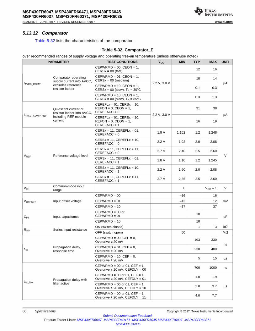
66
MSP430FR6047, MSP430FR60471, MSP430FR6045MSP430FR6037, MSP430FR60371, MSP430FR6035SLASEB7B –JUNE 2017–REVISED DECEMBER 2017 www.ti.com
Submit Documentation FeedbackProduct Folder Links: MSP430FR6047 MSP430FR60471 MSP430FR6045 MSP430FR6037 MSP430FR60371
MSP430FR6035
Specifications Copyright © 2017, Texas Instruments Incorporated
5.13.12 ComparatorTable 5-32 lists the characteristics of the comparator.
Table 5-32. Comparator_Eover recommended ranges of supply voltage and operating free-air temperature (unless otherwise noted)
PARAMETER TEST CONDITIONS VCC MIN TYP MAX UNIT
IAVCC_COMP
Comparator operatingsupply current into AVCC,excludes referenceresistor ladder
CEPWRMD = 00, CEON = 1,CERSx = 00 (fast)
2.2 V, 3.0 V
12 16
µA
CEPWRMD = 01, CEON = 1,CERSx = 00 (medium) 10 14
CEPWRMD = 10, CEON = 1,CERSx = 00 (slow), TA = 30°C 0.1 0.3
CEPWRMD = 10, CEON = 1,CERSx = 00 (slow), TA = 85°C 0.3 1.3
IAVCC_COMP_REF
Quiescent current ofresistor ladder into AVCC,including REF modulecurrent
CEREFLx = 01, CERSx = 10,REFON = 0, CEON = 1,CEREFACC = 0
2.2 V, 3.0 V
31 38
µACEREFLx = 01, CERSx = 10,REFON = 0, CEON = 1,CEREFACC = 1
16 19
VREF Reference voltage level
CERSx = 11, CEREFLx = 01,CEREFACC = 0 1.8 V 1.152 1.2 1.248
V
CERSx = 11, CEREFLx = 10,CEREFACC = 0 2.2 V 1.92 2.0 2.08
CERSx = 11, CEREFLx = 11,CEREFACC = 0 2.7 V 2.40 2.5 2.60
CERSx = 11, CEREFLx = 01,CEREFACC = 1 1.8 V 1.10 1.2 1.245
CERSx = 11, CEREFLx = 10,CEREFACC = 1 2.2 V 1.90 2.0 2.08
CERSx = 11, CEREFLx = 11,CEREFACC = 1 2.7 V 2.35 2.5 2.60
VICCommon-mode inputrange 0 VCC – 1 V
VOFFSET Input offset voltageCEPWRMD = 00 –16 16
mVCEPWRMD = 01 –12 12CEPWRMD = 10 –37 37
CIN Input capacitanceCEPWRMD = 00 orCEPWRMD = 01 10
pFCEPWRMD = 10 10
RSIN Series input resistanceON (switch closed) 1 3 kΩOFF (switch open) 50 MΩ
tPDPropagation delay,response time
CEPWRMD = 00, CEF = 0,Overdrive ≥ 20 mV 193 330
nsCEPWRMD = 01, CEF = 0,Overdrive ≥ 20 mV 230 400
CEPWRMD = 10, CEF = 0,Overdrive ≥ 20 mV 5 15 µs
tPD,filterPropagation delay withfilter active
CEPWRMD = 00 or 01, CEF = 1,Overdrive ≥ 20 mV, CEFDLY = 00 700 1000 ns
CEPWRMD = 00 or 01, CEF = 1,Overdrive ≥ 20 mV, CEFDLY = 01 1.0 1.9
µsCEPWRMD = 00 or 01, CEF = 1,Overdrive ≥ 20 mV, CEFDLY = 10 2.0 3.7
CEPWRMD = 00 or 01, CEF = 1,Overdrive ≥ 20 mV, CEFDLY = 11 4.0 7.7

67
MSP430FR6047, MSP430FR60471, MSP430FR6045MSP430FR6037, MSP430FR60371, MSP430FR6035
www.ti.com SLASEB7B –JUNE 2017–REVISED DECEMBER 2017
Submit Documentation FeedbackProduct Folder Links: MSP430FR6047 MSP430FR60471 MSP430FR6045 MSP430FR6037 MSP430FR60371
MSP430FR6035
SpecificationsCopyright © 2017, Texas Instruments Incorporated
Table 5-32. Comparator_E (continued)over recommended ranges of supply voltage and operating free-air temperature (unless otherwise noted)
PARAMETER TEST CONDITIONS VCC MIN TYP MAX UNIT
tEN_CMP Comparator enable time
CEON = 0 → 1, VIN+,VIN- from pins,Overdrive ≥ 20 mV,CEPWRMD = 00
0.9 1.5
µs
CEON = 0 → 1, VIN+,VIN- from pins,Overdrive ≥ 20 mV,CEPWRMD = 01
0.9 1.5
CEON = 0 → 1,VIN+, VIN- from pins,Overdrive ≥ 20 mV,CEPWRMD = 10
15 65
tEN_CMP_VREF
Comparator and referenceladder and referencevoltage enable time
CEON = 0 → 1, CEREFLX = 10,CERSx = 10 or 11,CEREF0 = CEREF1 = 0x0F,REFON = 0
120 220
µs
tEN_CMP_RLComparator and referenceladder enable time
CEON = 0 → 1, CEREFLX = 10,CERSx = 10, REFON = 1,CEREF0 = CEREF1 = 0x0F
10 30
VCE_REFReference voltage for agiven tap
VIN = reference into resistor ladder,n = 0 to 31
VIN ×(n +0.5)/ 32
VIN ×(n + 1)
/ 32
VIN ×(n + 1.5)
/ 32V
5.13.13 FRAMTable 5-33 lists the characteristics of the FRAM.
(1) Writing to FRAM does not require a setup sequence or additional power when compared to reading from FRAM. The FRAM readcurrent IREAD is included in the active mode current consumption, IAM,FRAM.
(2) FRAM does not require a special erase sequence.(3) N/A = Not applicable(4) Writing into FRAM is as fast as reading.(5) The maximum read (and write) speed is specified by fSYSTEM using the appropriate wait state settings (NWAITSx).
Table 5-33. FRAM Memoryover recommended ranges of supply voltage and operating free-air temperature (unless otherwise noted)
PARAMETER TJ MIN TYP MAX UNITRead and write endurance 1015 cycles
tRetention Data retention duration25°C 100
years70°C 4085°C 10
IWRITE Current to write into FRAM (1) IREAD nAIERASE Erase current (2) N/A (3) nAtWRITE Write time (4) tREAD ns
tREAD Read time (5) NWAITSx = 0 1 / fSYSTEM nsNWAITSx = 1 2 / fSYSTEM

68
MSP430FR6047, MSP430FR60471, MSP430FR6045MSP430FR6037, MSP430FR60371, MSP430FR6035SLASEB7B –JUNE 2017–REVISED DECEMBER 2017 www.ti.com
Submit Documentation FeedbackProduct Folder Links: MSP430FR6047 MSP430FR60471 MSP430FR6045 MSP430FR6037 MSP430FR60371
MSP430FR6035
Specifications Copyright © 2017, Texas Instruments Incorporated
5.13.14 USSTable 5-34 lists the USS recommended operating conditions.
Table 5-34. USS Recommended Operating ConditionsPARAMETER TEST CONDITIONS MIN TYP MAX UNIT
PVCC Analog supply voltage at PVCC pins for LDO operation 2.2 3.6 VPVCC Analog supply voltage at PVCC pins for USS operation 2.2 3.6 V
Table 5-35 lists the characteristics of the USS LDO.
Table 5-35. USS LDOover recommended ranges of supply voltage and operating free-air temperature (unless otherwise noted)
PARAMETER TEST CONDITIONS MIN TYP MAX UNITVCC-LDO Analog supply voltage at PVCC pins 2.2 3.6 VVUSS USS voltage 0 ≤ ILOAD ≤ ILOAD,MAX 1.52 1.6 1.65 V
tholdoff Hold off delay on power up
LBHDEL = 0 0
µsLBHDEL = 1 100LBHDEL = 2 200LBHDEL = 3 300
ttime-out Time-out on transition from OFF to READY 160 +tholdoff
µs
Table 5-36 lists the characteristics of the USS crystal.
Table 5-36. USSXTALover recommended ranges of supply voltage and operating free-air temperature (unless otherwise noted)
PARAMETER TEST CONDITIONS MIN TYP MAX UNITNphase_osc Integrated phase noise fosc = 4 MHz or 8 MHz, range = 10 kHz to 4 MHz –74 dBcFRQXTAL Resonator frequency 4 8 MHzDCosc Duty cycle 35% 65%
Iosc OSC supply current
fosc = 4 MHz or 8 MHz, CL = 18 pF, CS = 4 pF,fully settled, ceramic resonator 180
µAfosc = 4 MHz or 8 MHz, CL = 12 pF (4 MHz) or16 pF (8 MHz), CS = 7 pF, fully settled, crystal resonator 240
Aosc Oscillation allowance
fosc = 4 MHz, CL = 18 pF, CS = 4 pF, ceramic resonator 1500
Ωfosc = 4 MHz, CL = 12 pF, CS = 7 pF, crystal resonator 1000fosc = 8 MHz, CL = 18 pF, CS = 4 pF, ceramic resonator 500fosc = 8 MHz, CL = 16 pF, CS = 7 pF, crystal resonator 350
Tstart_osc Start-up time (gate)
fosc = 4 MHz, crystal resonator 2.8 4.6
msfosc = 8 MHz, crystal resonator 1 1.9fosc = 4 MHz, ceramic resonator 0.14 0.17fosc = 8 MHz, ceramic resonator 0.08 0.12
69
MSP430FR6047, MSP430FR60471, MSP430FR6045MSP430FR6037, MSP430FR60371, MSP430FR6035
www.ti.com SLASEB7B –JUNE 2017–REVISED DECEMBER 2017
Submit Documentation FeedbackProduct Folder Links: MSP430FR6047 MSP430FR60471 MSP430FR6045 MSP430FR6037 MSP430FR60371
MSP430FR6035
SpecificationsCopyright © 2017, Texas Instruments Incorporated
Table 5-37 lists the characteristics of the USS HSPLL.
Table 5-37. USS HSPLLover recommended ranges of supply voltage and operating free-air temperature (unless otherwise noted)
PARAMETER TEST CONDITIONS MIN TYP MAX UNITPLL_CLKin Input clock to HSPLL 4 8 MHzPLL_CLKout Output clock from HSPLL 68 80 MHz
LOCKpwr Lock time from PLL power up
Reference clock = PLL_CLKin,Sequence: Set USS.CTL.USSPWRUP bit = 1, thenmeasure the time between PSQ_PLLUP (internalcontrol signal) is set to 1 andHSPLL.CTL.PLL_LOCK is set to 1
64 cycles
Table 5-38 lists the characteristics of the USS SDHS.
(1) Informative parameter, not characterized(2) SNR as specified, SINAD and THD not specified over complete signal chain
Table 5-38. USS SDHSover recommended ranges of supply voltage and operating free-air temperature (unless otherwise noted)
PARAMETER TEST CONDITIONS MIN TYP MAX UNIT
VsdhsSDHS power domainsupply voltage Vsdhs = Vuss 1.52 1.6 1.65 V
Isdhs_product
Operating supplycurrent into AVCC andDVCC
Includes PLL, PGA, SDHS, and DTC,modulator clock = 80 MHz, output data rate = 8 Msps 5.2 mA
VSDHS_FS Full-scale voltage (1) 755 mVpp
VIN_SDHS_MAXMaximum input voltageto SDHS (1) 600 mVpp
fmod Modulator clock (1) 68 80 MHz
BWmodFrequency at –3-dBSNR
Modulator clock = 80 MHz, modulator only (no filter isenabled) 1.5 MHz
SNR Signal-to-noise ratio (2)
Bandwidth up to1.5 MHz, PGA gain: again from the PGA gaintable for the maximumSNR
Input signal level = 1000 mVpp,PVCC = 3.0 V, fmod = 80 MHz,OSR = 20
58.5 62.5
dB
Bandwidth up to1.5 MHz, PGA gain: again from the PGA gaintable for the maximumSNR
Input signal level = 760 mVpp,PVCC = 2.5 V, fmod = 80 MHz,OSR = 20
57.5 62
Bandwidth up to1.5 MHz, PGA gain: again from the PGA gaintable for the maximumSNR
Input signal level = 200 mVpp,PVCC = 2.5 V, fmod = 80 MHz,OSR = 20
54.5 57
Bandwidth up to1.5 MHz, PGA gain: again from the PGA gaintable for the maximumSNR
Input signal level = 100 mVpp,PVCC = 2.5 V, fmod = 80 MHz,OSR = 20
49 53
Bandwidth up to1.5 MHz, PGA gain: again from the PGA gaintable for the maximumSNR
Input signal level = 30 mVpp,PVCC = 2.5 V, fmod = 80 MHz,OSR = 20
38.5 43
tMOD_SettleSDHS settling time(PGA + modulator)
TM2 – TM1, AUTOSSDIS = 0, 1% of settled DC level 40µs
TM2 – TM1, AUTOSSDIS = 1, 1% of settled DC level 40DROUTsdhs Output data rate 8 Msps

70
MSP430FR6047, MSP430FR60471, MSP430FR6045MSP430FR6037, MSP430FR60371, MSP430FR6035SLASEB7B –JUNE 2017–REVISED DECEMBER 2017 www.ti.com
Submit Documentation FeedbackProduct Folder Links: MSP430FR6047 MSP430FR60471 MSP430FR6045 MSP430FR6037 MSP430FR60371
MSP430FR6035
Specifications Copyright © 2017, Texas Instruments Incorporated
Table 5-39 lists the characteristics of the USS PHY outputs.
Table 5-39. USS PHY Output Stageover recommended ranges of supply voltage and operating free-air temperature (unless otherwise noted)
PARAMETER TEST CONDITIONS MIN TYP MAX UNITPVCC PHY supply voltage PVCC = VCC, PVSS = VSS 2.2 3.6 V
RDSonTOutput impedance of CH0OUT and CH1OUT forhigh and low side (trimmed at 3-V PVDD) PVCC ≥ 2.5 V 3 Ω
RTermTermination impedance of CH0OUT andCH1OUT toward PVSS (trimmed) PVCC ≥ 2.5 V 3 Ω
DrvM High-side to low-side drive mismatch (trimmed) PVCC ≥ 2.5 V 5% 12.5%TermM Termination to drive mismatch (trimmed) PVCC ≥ 2.5 V 5% 12.5%fMAX Maximum output frequency PVCC = VCC (2.5 V to 3.6 V) 4.5 MHzCSUPP Supply buffering capacitance (low ESR type) PVCC = VCC 22 100 µFRSUPP Series resistance to CSUPP PVCC = VCC 22 Ω
Table 5-40 lists the characteristics of the USS PHY inputs.
Table 5-40. USS PHY Input Stage, Multiplexerover recommended ranges of supply voltage and operating free-air temperature (unless otherwise noted)
PARAMETER TEST CONDITIONS MIN TYP MAX UNIT
VIN Input voltage on CH0IN or CH1IN PVCC = VCC, PVSS = VSSPVSS –
0.3 1.8 V
Table 5-41 lists the characteristics of the USS PGA.
(1) See the PGA Gain table in the MSP430FR58xx, MSP430FR59xx, and MSP430FR6xx Family User's Guide.
Table 5-41. USS PGAover recommended ranges of supply voltage and operating free-air temperature (unless otherwise noted)
PARAMETER TEST CONDITIONS MIN TYP MAX UNITPVcc Supply voltage 2.2 3.6 VGN Gain (1) –6.5 30.8 dBVinr1 Input range 2.2 V ≤ PVCC 30 800 mVppVinr2 Input range 2.5 V ≤ PVCC 30 1000 mVpp
Vinrperf
Recommended inputrange for maximumperformance
2.5 V ≤ PVCC 30 800 mVpp
Gtol Gain tolerance Full PGA gain range, VOUT = 600 mV –1.5 1.5 dB
GTdriftGain drift withtemperature Full PGA gain range, VOUT = 600 mV 0.0019 dB/
GVdrift Gain drift with voltage Full PGA gain range, VOUT = 600 mV 0.15 dB/VtSET Gain settling time Gain setting: from 0 dB to 6 dB, to ±5% 0.65 1.4 µs
DCoffsetDC offset (PGA andSDHS) Full PGA gain range, measured at SDHS output 5.5 mV
DCdriftDC offset drift (PGAand SDHS) Full PGA gain range, measured at SDHS output 4.7 µV/
PSRR_AC AC power supplyrejection ratio
VCC = 3 V + 50 mVpp × sin (2π × fC)where fC = 1 MHz, VIN = ground,PSRR_AC = 20log(VOUT / 50 mV)
PGA gain = 0 dB –41dBPGA gain = 10 dB –37
PGA gain = 30 dB –19

71
MSP430FR6047, MSP430FR60471, MSP430FR6045MSP430FR6037, MSP430FR60371, MSP430FR6035
www.ti.com SLASEB7B –JUNE 2017–REVISED DECEMBER 2017
Submit Documentation FeedbackProduct Folder Links: MSP430FR6047 MSP430FR60471 MSP430FR6045 MSP430FR6037 MSP430FR60371
MSP430FR6035
SpecificationsCopyright © 2017, Texas Instruments Incorporated
Table 5-42 lists the characteristics of the USS bias voltage generator.
Table 5-42. USS Bias Voltage Generatorover recommended ranges of supply voltage and operating free-air temperature (unless otherwise noted)
PARAMETER TEST CONDITIONS MIN TYP MAX UNIT
Vexc_biasExcitation bias voltage(coupling capacitors) PVCC = VCC (2.2 V to 3.6 V)
EXCBIAS = 0 200
mVEXCBIAS = 1 300EXCBIAS = 2 400EXCBIAS = 3 600
RVBEImpedance of excitation biasgenerator
PVCC = VCC (2.2 V to 3.6 V) BIMP = 0 450
ΩBIMP = 1 850BIMP = 2 1450BIMP = 3 2900
tSBE Excitation bias settling time PVCC = VCC (2.2 V to 3.6 V), to 0.1% end value,RET = 200 Ω, CK + C0P = 1 nF, BIMP = 2 20 µs
Vpga_biasPGA bias voltage (couplingcapacitors) PVCC = VCC (2.2 V to 3.6 V)
PGABIAS = 0 750
mVPGABIAS = 1 800PGABIAS = 2 900PGABIAS = 3 950
RVBAImpedance of acquisition biasgenerator
PVCC = VCC (2.2 V to 3.6 V) BIMP = 0 500
ΩBIMP = 1 900BIMP = 2 1500BIMP = 3 2950
tSBA Acquisition bias settling time PVCC = VCC (2.2 V to 3.6 V), to 0.1% end value,RET = 200 Ω, CK + C0P = 1 nF, BIMP = 2 22 µs
5.13.15 Emulation and DebugTable 5-43 lists the characteristics of the JTAG and SBW interface.
(1) Tools that access the Spy-Bi-Wire and the BSL interfaces must wait for the tSBW,En time after the first transition of the TEST/SBWTCKpin (low to high), before the second transition of the pin (high to low) during the entry sequence.
(2) fTCK may be restricted to meet the timing requirements of the module selected.
Table 5-43. JTAG and Spy-Bi-Wire Interfaceover recommended ranges of supply voltage and operating free-air temperature (unless otherwise noted)
PARAMETER VCC MIN TYP MAX UNITIJTAG Supply current adder when JTAG active (but not clocked) 2.2 V, 3.0 V 40 100 μAfSBW Spy-Bi-Wire input frequency 2.2 V, 3.0 V 0 10 MHztSBW,Low Spy-Bi-Wire low clock pulse duration 2.2 V, 3.0 V 0.04 15 μs
tSBW, EnSpy-Bi-Wire enable time (TEST high to acceptance of first clockedge) (1) 2.2 V, 3.0 V 110 μs
tSBW,Rst Spy-Bi-Wire return to normal operation time 15 100 μs
fTCK TCK input frequency, 4-wire JTAG (2) 2.2 V 0 16MHz
3.0 V 0 16Rinternal Internal pulldown resistance on TEST 2.2 V, 3.0 V 20 35 50 kΩ
fTCLKTCLK/MCLK frequency during JTAG access, no FRAM access(limited by fSYSTEM) 16 MHz
tTCLK,Low/High TCLK low or high clock pulse duration, no FRAM access 25 ns
fTCLK,FRAMTCLK/MCLK frequency during JTAG access, including FRAM access(limited by fSYSTEM with no FRAM wait states) 4 MHz
tTCLK,FRAM,Low/High
TCLK low or high clock pulse duration, including FRAM accesses 100 ns
72
MSP430FR6047, MSP430FR60471, MSP430FR6045MSP430FR6037, MSP430FR60371, MSP430FR6035SLASEB7B –JUNE 2017–REVISED DECEMBER 2017 www.ti.com
Submit Documentation FeedbackProduct Folder Links: MSP430FR6047 MSP430FR60471 MSP430FR6045 MSP430FR6037 MSP430FR60371
MSP430FR6035
Detailed Description Copyright © 2017, Texas Instruments Incorporated
6 Detailed Description
6.1 OverviewThe TI MSP430FR60xx(1) family of ultra-low-power microcontrollers consists of several devices featuringdifferent sets of peripherals. The architecture, combined with seven low-power modes, is optimized toachieve extended battery life for example in portable measurement applications. The devices features apowerful 16-bit RISC CPU, 16-bit registers, and constant generators that contribute to maximum codeefficiency.
The device is an MSP430FR6xx family device with Ultrasonic Sensing Solution (USS), Low-EnergyAccelerator (LEA), up to six 16-bit timers, up to six eUSCIs that support UART, SPI, and I2C, acomparator, a hardware multiplier, an AES accelerator, a 6-channel DMA, an RTC module with alarmcapabilities, up to 76 I/O pins, and a high-performance 12-bit ADC. The MSP430FR60xx(1) devices alsoinclude an LCD module with contrast control for displays with up to 264 segments.
6.2 CPUThe MSP430 CPU has a 16-bit RISC architecture that is highly transparent to the application. Alloperations, other than program-flow instructions, are performed as register operations in conjunction withseven addressing modes for source operand and four addressing modes for destination operand.
The CPU is integrated with 16 registers that provide reduced instruction execution time. The register-to-register operation execution time is one cycle of the CPU clock.
Four of the registers, R0 to R3, are dedicated as program counter, stack pointer, status register, andconstant generator, respectively. The remaining registers are general-purpose registers.
Peripherals are connected to the CPU using data, address, and control buses. The peripherals can bemanaged with all instructions.
The instruction set consists of the original 51 instructions with three formats and seven address modesand additional instructions for the expanded address range. Each instruction can operate on word andbyte data.
6.3 Ultrasonic Sensing Solution (USS) ModuleThe USS module provides a high-precision ultrasonic sensing solution. The USS module is asophisticated system that consists of six submodules:• UUPS (universal USS power supply)• HSPLL (high-speed PLL) with oscillator• ASQ (acquisition sequencer)• PHY (physical interface)• PPG (programmable pulse generator) with low-output-impedance driver• PGA (programmable gain amplifier)• SDHS (sigma-delta high-speed ADC) with DTC (data transfer controller)
The submodules have different roles, and together they enable high-precision data acquisition inultrasonic applications. See the dedicated chapter for each submodule in the MSP430FR58xx,MSP430FR59xx, and MSP430FR6xx Family User's Guide.
The USS module performs complete measurement sequence without CPU involvement to achieve ultra-low power consumption for ultrasonic metrology. Figure 6-1 shows the USS subsystem block diagram.The USS module has dedicated I/O pins without secondary functions. See the Ultrasonic Sensing Solution(USS) chapter in the MSP430FR58xx, MSP430FR59xx, and MSP430FR6xx Family User's Guide fordetails.
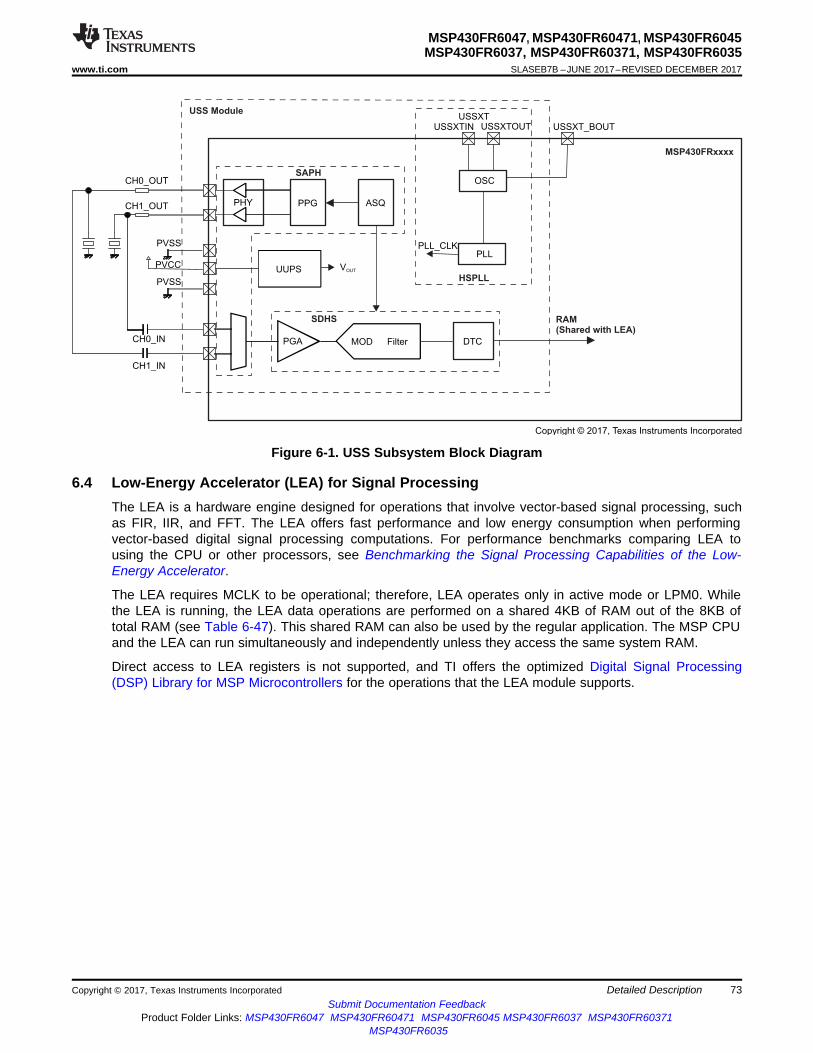
PGA
VOUT
PVSS
PLL
USSXT
PVCC
PPG
MOD Filter
USSXTIN USSXTOUT
DTC
RAM(Shared with LEA)
UUPS
PHY ASQ
PLL_CLK
USS Module
PVSS
CH0_OUT
CH1_OUT
CH0_IN
CH1_IN
OSC
USSXT_BOUT
SDHS
SAPH
HSPLL
MSP430FRxxxx
Copyright © 2017, Texas Instruments Incorporated
73
MSP430FR6047, MSP430FR60471, MSP430FR6045MSP430FR6037, MSP430FR60371, MSP430FR6035
www.ti.com SLASEB7B –JUNE 2017–REVISED DECEMBER 2017
Submit Documentation FeedbackProduct Folder Links: MSP430FR6047 MSP430FR60471 MSP430FR6045 MSP430FR6037 MSP430FR60371
MSP430FR6035
Detailed DescriptionCopyright © 2017, Texas Instruments Incorporated
Figure 6-1. USS Subsystem Block Diagram
6.4 Low-Energy Accelerator (LEA) for Signal ProcessingThe LEA is a hardware engine designed for operations that involve vector-based signal processing, suchas FIR, IIR, and FFT. The LEA offers fast performance and low energy consumption when performingvector-based digital signal processing computations. For performance benchmarks comparing LEA tousing the CPU or other processors, see Benchmarking the Signal Processing Capabilities of the Low-Energy Accelerator.
The LEA requires MCLK to be operational; therefore, LEA operates only in active mode or LPM0. Whilethe LEA is running, the LEA data operations are performed on a shared 4KB of RAM out of the 8KB oftotal RAM (see Table 6-47). This shared RAM can also be used by the regular application. The MSP CPUand the LEA can run simultaneously and independently unless they access the same system RAM.
Direct access to LEA registers is not supported, and TI offers the optimized Digital Signal Processing(DSP) Library for MSP Microcontrollers for the operations that the LEA module supports.

Copyright © 2017, Texas Instruments IncorporatedDetailed DescriptionSubmit Documentation Feedback
Product Folder Links: MSP430FR6047 MSP430FR60471 MSP430FR6045 MSP430FR6037 MSP430FR60371MSP430FR6035
74
MSP430FR6047, MSP430FR60471, MSP430FR6045MSP430FR6037, MSP430FR60371, MSP430FR6035SLASEB7B –JUNE 2017–REVISED DECEMBER 2017 www.ti.com
6.5 Operating ModesThe MCU has one active mode and seven software-selectable low-power modes of operation. An interrupt event can wake up the device from low-power modes LPM0 to LPM4, service the request, and return to the low-power mode on return from the interrupt program. Low-power modesLPM3.5 and LPM4.5 disable the core supply to minimize power consumption. Table 6-1 lists the operating modes and the clocks and peripheralsthat are available in each.
(1) FRAM is disabled in the FRAM controller (FRCTL_A).(2) Disabling the FRAM through the FRAM controller (FRCTL_A) allows the application to lower the LPM current consumption but the wake-up time increases when FRAM is accessed (for
example, to fetch an interrupt vector). For a wakeup that does not involve FRAM (for example, a DMA transfer to RAM) the wake-up time is not increased.(3) All clocks disabled(4) Only while the LEA is performing a task enabled by the CPU during AM. The LEA cannot be enabled in LPM0.(5) See Section 6.5.2, which describes the use of peripherals in LPM3 and LPM4.(6) Unclocked peripherals are peripherals that do not require a clock source to operate; for example, the comparator and REF, or the eUSCI when operated as an SPI slave.(7) Controlled by SMCLKOFF.
Table 6-1. Operating ModesMODE AM LPM0 LPM1 LPM2 LPM3 LPM4 LPM3.5 LPM4.5
ACTIVEACTIVE,FRAMOFF (1)
CPU OFF (2) CPU OFF STANDBY STANDBY OFF RTC ONLY SHUTDOWNWITH SVS
SHUTDOWNWITHOUT SVS
Maximum system clock 16 MHz 16 MHz 16 MHz 50 kHz 50 kHz 0 (3) 50 kHz 0 (3)
Typical current consumption,TA = 25°C 103 µA/MHz 65 µA/MHz 70 µA at 1 MHz 35 µA at 1 MHz 0.7 µA 0.4 µA 0.3 µA 0.25 µA 0.2 µA 0.02 µA
Typical wake-up time N/A instant 6 µs 6 µs 7 µs 7 µs 250 µs 250 µs 1000 µs
Wake-up events N/A all all
LFRTCI/O
Comp
LFRTCI/O
Comp
I/OComp
RTCI/O I/O
CPU on off off off off off reset reset
USS on on off off off off reset reset
LEA on on (4) off off off off off reset reset
FRAM on off (1) standby(or off (1)) off off off off off off
High-frequency peripherals available available available off off off reset reset
Low-frequency peripherals available available available available available (5) off RTCMTIF reset
Unclocked peripherals (6) available available available available available (5) available (5) reset reset
MCLK on on (4) off off off off off off off
SMCLK optional (7) optional (7) optional (7) off off off off off
ACLK on on on on on off off off
Full retention yes yes yes yes yes yes no no
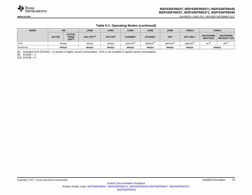
Copyright © 2017, Texas Instruments Incorporated Detailed DescriptionSubmit Documentation Feedback
Product Folder Links: MSP430FR6047 MSP430FR60471 MSP430FR6045 MSP430FR6037 MSP430FR60371MSP430FR6035
75
MSP430FR6047, MSP430FR60471, MSP430FR6045MSP430FR6037, MSP430FR60371, MSP430FR6035
www.ti.com SLASEB7B –JUNE 2017–REVISED DECEMBER 2017
Table 6-1. Operating Modes (continued)MODE AM LPM0 LPM1 LPM2 LPM3 LPM4 LPM3.5 LPM4.5
ACTIVEACTIVE,FRAMOFF (1)
CPU OFF (2) CPU OFF STANDBY STANDBY OFF RTC ONLY SHUTDOWNWITH SVS
SHUTDOWNWITHOUT SVS
(8) Activated SVS (SVSHE = 1) results in higher current consumption. SVS is not included in typical current consumption.(9) SVSHE = 1(10) SVSHE = 0
SVS always always always optional (8) optional (8) optional (8) optional (8) on (9) off (10)
Brownout always always always always always always always always

76
MSP430FR6047, MSP430FR60471, MSP430FR6045MSP430FR6037, MSP430FR60371, MSP430FR6035SLASEB7B –JUNE 2017–REVISED DECEMBER 2017 www.ti.com
Submit Documentation FeedbackProduct Folder Links: MSP430FR6047 MSP430FR60471 MSP430FR6045 MSP430FR6037 MSP430FR60371
MSP430FR6035
Detailed Description Copyright © 2017, Texas Instruments Incorporated
(1) Peripherals are in a state that requires or uses a clock with a "high" frequency of more than 50 kHz(2) Peripherals are in a state that requires or uses a clock with a "low" frequency of 50 kHz or less.(3) Peripherals are in a state that does not require or does not use an internal clock.(4) The DMA always transfers data in active mode but can wait for a trigger in any low-power mode. A DMA trigger during a low-power
mode causes a temporary transition into active mode for the time of the transfer.(5) This peripheral operates during active mode only and will delay the transition into a low-power mode until its operation is completed.
6.5.1 Peripherals in Low-Power ModesPeripherals can be in different states that affect the achievable power modes of the device. The statesdepend on the operational modes of the peripherals (see Table 6-2). The states are:• A peripheral is in a "high-frequency state" if it requires or uses a clock with a "high" frequency of more
than 50 kHz.• A peripheral is in a "low-frequency state" if it requires or uses a clock with a "low" frequency of 50 kHz
or less.• A peripheral is in an "unclocked state" if it does not require or use an internal clock.
If the CPU requests a power mode that does not support the current state of all active peripherals, thedevice does not enter the requested power mode, but it does enter a power mode that still supports thecurrent state of the peripherals, except if an external clock is used. If an external clock is used, theapplication must use the correct frequency range for the requested power mode.
Table 6-2. Peripheral States
PERIPHERAL IN HIGH-FREQUENCY STATE (1) IN LOW-FREQUENCY STATE (2) IN UNCLOCKED STATE (3)
WDT Clocked by SMCLK Clocked by ACLK Not applicableDMA (4) Not applicable Not applicable Waiting for a triggerRTC_C Not applicable Clocked by LFXT Not applicableLCD_C Not applicable Clocked by ACLK or VLOCLK Not applicable
Timer_A, TAx Clocked by SMCLK orclocked by external clock >50 kHz
Clocked by ACLK orclocked by external clock ≤50 kHz Clocked by external clock ≤50 kHz
Timer_B, TBx Clocked by SMCLK orclocked by external clock >50 kHz
Clocked by ACLK orclocked by external clock ≤50 kHz Clocked by external clock ≤50 kHz
eUSCI_Ax inUART mode Clocked by SMCLK Clocked by ACLK Waiting for first edge of START bit
eUSCI_Ax in SPImaster mode Clocked by SMCLK Clocked by ACLK Not applicable
eUSCI_Ax in SPIslave mode Clocked by external clock >50 kHz Clocked by external clock ≤50 kHz Clocked by external clock ≤50 kHz
eUSCI_Bx in I2Cmaster mode
Clocked by SMCLK orclocked by external clock >50 kHz
Clocked by ACLK orclocked by external clock ≤50 kHz Not applicable
eUSCI_Bx in I2Cslave mode Clocked by external clock >50 kHz Clocked by external clock ≤50 kHz Waiting for START condition or
clocked by external clock ≤50 kHzeUSCI_Bx in SPImaster mode Clocked by SMCLK Clocked by ACLK Not applicable
eUSCI_Bx in SPIslave mode Clocked by external clock >50 kHz Clocked by external clock ≤50 kHz Clocked by external clock ≤50 kHz
ADC12_B Clocked by SMCLK or by MODOSC Clocked by ACLK Waiting for a triggerREF_A Not applicable Not applicable AlwaysCOMP_E Not applicable Not applicable AlwaysCRC (5) Not applicable Not applicable Not applicableMPY (5) Not applicable Not applicable Not applicableAES (5) Not applicable Not applicable Not applicable

0FFFFh
JTAG Password
BSL Password
Reset Vector
InterruptVectors
Signatures
Reserved
0FF88h
0FF80h
0FFE0h
77
MSP430FR6047, MSP430FR60471, MSP430FR6045MSP430FR6037, MSP430FR60371, MSP430FR6035
www.ti.com SLASEB7B –JUNE 2017–REVISED DECEMBER 2017
Submit Documentation FeedbackProduct Folder Links: MSP430FR6047 MSP430FR60471 MSP430FR6045 MSP430FR6037 MSP430FR60371
MSP430FR6035
Detailed DescriptionCopyright © 2017, Texas Instruments Incorporated
6.5.2 Idle Currents of Peripherals in LPM3 and LPM4Most peripherals can be operational in LPM3 if clocked by ACLK. Some modules are operational in LPM4,because they do not require a clock to operate (for example, the comparator). Activating a peripheral inLPM3 or LPM4 increases the current consumption due to its active supply current contribution but alsodue to an additional idle current. To reduce the idle current adder, certain peripherals are groupedtogether. To achieve optimal current consumption, use modules within one group and limit the number ofgroups with active modules. Table 6-3 lists the peripheral groups. Modules not listed in this table are eitheralready included in the standard LPM3 current consumption or cannot be used in LPM3 or LPM4.
The idle current adder is very small at room temperature (25°C) but increases at high temperatures(85°C); see the IIDLE current parameters in for details.
Table 6-3. Peripheral Groups
GROUP A GROUP B GROUP CTimer TA1 Timer TA0 Timer TA4Timer TA2 Timer TA3 eUSCI_A2Timer TB0 Comparator eUSCI_A3eUSCI_A0 ADC12_B eUSCI_B1eUSCI_A1 REF_A LCD_CeUSCI_B0
6.6 Interrupt Vector Table and SignaturesThe interrupt vectors, the power-up start address, and signatures are in the address range 0FFFFh to0FF80h. Figure 6-2 summarizes the content of this address range.
Figure 6-2. Interrupt Vectors, Signatures and Passwords
The power-up start address or reset vector is at 0FFFFh to 0FFFEh. It contains the 16-bit address pointingto the start address of the application program.
The interrupt vectors start at 0FFFDh and extend to lower addresses. Each vector contains the 16-bitaddress of the appropriate interrupt-handler instruction sequence. Table 6-4 shows the device-specificinterrupt vector locations.
The vectors programmed into the address range from 0FFFFh to 0FFE0h are used as BSL password (ifenabled by the corresponding signature).

78
MSP430FR6047, MSP430FR60471, MSP430FR6045MSP430FR6037, MSP430FR60371, MSP430FR6035SLASEB7B –JUNE 2017–REVISED DECEMBER 2017 www.ti.com
Submit Documentation FeedbackProduct Folder Links: MSP430FR6047 MSP430FR60471 MSP430FR6045 MSP430FR6037 MSP430FR60371
MSP430FR6035
Detailed Description Copyright © 2017, Texas Instruments Incorporated
(1) Multiple source flags(2) A reset is generated if the CPU tries to fetch instructions from within peripheral space.(3) (Non)maskable: the individual interrupt enable bit can disable an interrupt event, but the general interrupt enable cannot disable it.(4) Only on devices with ADC, otherwise reserved.
The signatures start at 0FF80h and extend to higher addresses. Signatures are evaluated during devicestart-up. Table 6-5 shows the device-specific signature locations.
A JTAG password can be programmed starting from address 0FF88h and extending to higher addresses.The password can extend into the interrupt vector locations using the interrupt vector addresses asadditional bits for the password. The length of the JTAG password depends on the JTAG signature.
See the chapter System Resets, Interrupts, and Operating Modes, System Control Module (SYS) in theMSP430FR58xx, MSP430FR59xx, and MSP430FR6xx Family User's Guide for details.
Table 6-4. Interrupt Sources, Flags, and Vectors
INTERRUPT SOURCE INTERRUPT FLAG SYSTEMINTERRUPT
WORDADDRESS PRIORITY
System ResetPower up, brownout, supply
supervisorExternal reset RST
Watchdog time-out (watchdogmode)
WDT, FRCTL MPU, CS,PMM password violation
FRAM uncorrectable bit errordetection
MPU segment violationSoftware POR, BOR
SVSHIFGPMMRSTIFG
WDTIFGWDTPW, FRCTLPW, MPUPW, CSPW, PMMPW
UBDIFGMPUSEG1IFG, MPUSEG2IFG, MPUSEG3IFG
PMMPORIFG, PMMBORIFG(SYSRSTIV) (1) (2)
Reset 0FFFEh Highest
System NMIVacant memory access
JTAG mailboxFRAM access time error
FRAM write protection errorFRAM bit error detectionMPU segment violation
VMAIFGJMBINIFG, JMBOUTIFG
ACCTEIFG, WPIFGCBDIFG, UBDIFG
MPUSEG1IFG, MPUSEG2IFG, MPUSEG3IFG(SYSSNIV) (1) (3)
(Non)maskable 0FFFCh
User NMIExternal NMIOscillator fault
LEA RAM access conflict
NMIIFG, OFIFGDACCESSIFG
(SYSUNIV) (1) (3)(Non)maskable 0FFFAh
Comparator_E CEIFG, CEIIFG(CEIV) (1) Maskable 0FFF8h
TB0 TB0CCR0.CCIFG Maskable 0FFF6h
TB0TB0CCR1.CCIFG to TB0CCR6.CCIFG,
TB0CTL.TBIFG(TB0IV) (1)
Maskable 0FFF4h
Watchdog timer (interval timermode) WDTIFG Maskable 0FFF2h
eUSCI_A0 receive or transmit
UCA0IFG: UCRXIFG, UCTXIFG (SPI mode)UCA0IFG: UCSTTIFG, UCTXCPTIFG, UCRXIFG,
UCTXIFG (UART mode)(UCA0IV) (1)
Maskable 0FFF0h
eUSCI_B0 receive or transmit
UCB0IFG: UCRXIFG, UCTXIFG (SPI mode)UCB0IFG: UCALIFG, UCNACKIFG, UCSTTIFG,UCSTPIFG, UCRXIFG0, UCTXIFG0, UCRXIFG1,UCTXIFG1, UCRXIFG2, UCTXIFG2, UCRXIFG3,UCTXIFG3, UCCNTIFG, UCBIT9IFG (I2C mode)
(UCB0IV) (1)
Maskable 0FFEEh
ADC12_B
ADC12IFG0 to ADC12IFG31ADC12LOIFG, ADC12INIFG, ADC12HIIFG,
ADC12RDYIFG, ADC21OVIFG, ADC12TOVIFG(ADC12IV) (1) (4)
Maskable 0FFECh
TA0 TA0CCR0.CCIFG Maskable 0FFEAh
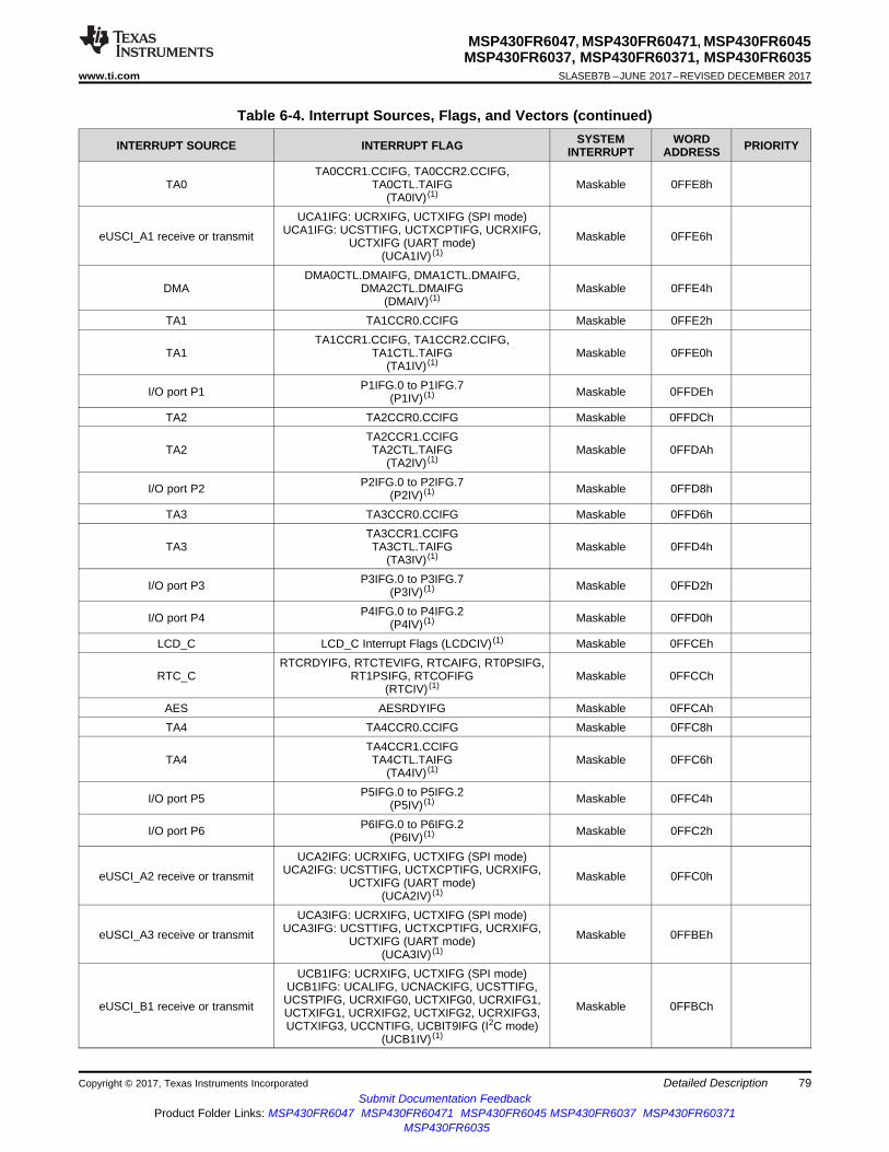
79
MSP430FR6047, MSP430FR60471, MSP430FR6045MSP430FR6037, MSP430FR60371, MSP430FR6035
www.ti.com SLASEB7B –JUNE 2017–REVISED DECEMBER 2017
Submit Documentation FeedbackProduct Folder Links: MSP430FR6047 MSP430FR60471 MSP430FR6045 MSP430FR6037 MSP430FR60371
MSP430FR6035
Detailed DescriptionCopyright © 2017, Texas Instruments Incorporated
Table 6-4. Interrupt Sources, Flags, and Vectors (continued)
INTERRUPT SOURCE INTERRUPT FLAG SYSTEMINTERRUPT
WORDADDRESS PRIORITY
TA0TA0CCR1.CCIFG, TA0CCR2.CCIFG,
TA0CTL.TAIFG(TA0IV) (1)
Maskable 0FFE8h
eUSCI_A1 receive or transmit
UCA1IFG: UCRXIFG, UCTXIFG (SPI mode)UCA1IFG: UCSTTIFG, UCTXCPTIFG, UCRXIFG,
UCTXIFG (UART mode)(UCA1IV) (1)
Maskable 0FFE6h
DMADMA0CTL.DMAIFG, DMA1CTL.DMAIFG,
DMA2CTL.DMAIFG(DMAIV) (1)
Maskable 0FFE4h
TA1 TA1CCR0.CCIFG Maskable 0FFE2h
TA1TA1CCR1.CCIFG, TA1CCR2.CCIFG,
TA1CTL.TAIFG(TA1IV) (1)
Maskable 0FFE0h
I/O port P1 P1IFG.0 to P1IFG.7(P1IV) (1) Maskable 0FFDEh
TA2 TA2CCR0.CCIFG Maskable 0FFDCh
TA2TA2CCR1.CCIFGTA2CTL.TAIFG
(TA2IV) (1)Maskable 0FFDAh
I/O port P2 P2IFG.0 to P2IFG.7(P2IV) (1) Maskable 0FFD8h
TA3 TA3CCR0.CCIFG Maskable 0FFD6h
TA3TA3CCR1.CCIFGTA3CTL.TAIFG
(TA3IV) (1)Maskable 0FFD4h
I/O port P3 P3IFG.0 to P3IFG.7(P3IV) (1) Maskable 0FFD2h
I/O port P4 P4IFG.0 to P4IFG.2(P4IV) (1) Maskable 0FFD0h
LCD_C LCD_C Interrupt Flags (LCDCIV) (1) Maskable 0FFCEh
RTC_CRTCRDYIFG, RTCTEVIFG, RTCAIFG, RT0PSIFG,
RT1PSIFG, RTCOFIFG(RTCIV) (1)
Maskable 0FFCCh
AES AESRDYIFG Maskable 0FFCAhTA4 TA4CCR0.CCIFG Maskable 0FFC8h
TA4TA4CCR1.CCIFGTA4CTL.TAIFG
(TA4IV) (1)Maskable 0FFC6h
I/O port P5 P5IFG.0 to P5IFG.2(P5IV) (1) Maskable 0FFC4h
I/O port P6 P6IFG.0 to P6IFG.2(P6IV) (1) Maskable 0FFC2h
eUSCI_A2 receive or transmit
UCA2IFG: UCRXIFG, UCTXIFG (SPI mode)UCA2IFG: UCSTTIFG, UCTXCPTIFG, UCRXIFG,
UCTXIFG (UART mode)(UCA2IV) (1)
Maskable 0FFC0h
eUSCI_A3 receive or transmit
UCA3IFG: UCRXIFG, UCTXIFG (SPI mode)UCA3IFG: UCSTTIFG, UCTXCPTIFG, UCRXIFG,
UCTXIFG (UART mode)(UCA3IV) (1)
Maskable 0FFBEh
eUSCI_B1 receive or transmit
UCB1IFG: UCRXIFG, UCTXIFG (SPI mode)UCB1IFG: UCALIFG, UCNACKIFG, UCSTTIFG,UCSTPIFG, UCRXIFG0, UCTXIFG0, UCRXIFG1,UCTXIFG1, UCRXIFG2, UCTXIFG2, UCRXIFG3,UCTXIFG3, UCCNTIFG, UCBIT9IFG (I2C mode)
(UCB1IV) (1)
Maskable 0FFBCh

80
MSP430FR6047, MSP430FR60471, MSP430FR6045MSP430FR6037, MSP430FR60371, MSP430FR6035SLASEB7B –JUNE 2017–REVISED DECEMBER 2017 www.ti.com
Submit Documentation FeedbackProduct Folder Links: MSP430FR6047 MSP430FR60471 MSP430FR6045 MSP430FR6037 MSP430FR60371
MSP430FR6035
Detailed Description Copyright © 2017, Texas Instruments Incorporated
Table 6-4. Interrupt Sources, Flags, and Vectors (continued)
INTERRUPT SOURCE INTERRUPT FLAG SYSTEMINTERRUPT
WORDADDRESS PRIORITY
I/O Port P7 P7IFG.0 to P7IFG.2(P7IV) (1) Maskable 0FFBAh
I/O Port P8 P8IFG.0 to P8IFG.2(P8IV) (1) Maskable 0FFB8h
I/O Port P9 P9IFG.0 to P9IFG.2(P9IV) (1) Maskable 0FFB6h
LEA CMDIFG, SDIIFG, OORIFG, TIFG, COVLIFG(LEAIV) (1) Maskable 0FFB4h
UUPS PTMOUT, PREQIG(IIDX) (1) Maskable 0FFB2h
HSPLL PLLUNLOCK(IIDX) (1) Maskable 0FFB0h
SAPH DATAERR, TAMTO, SEQDN, PNGDN(IIDX) (1) Maskable 0FFAEh
SDHSOVF, ACQDONE, SSTRG, DTRDY, WINHI,
WINLO(IIDX) (1)
Maskable 0FFACh Lowest
(1) Must not contain 0AAAAh if used as the JTAG password.
Table 6-5. Signatures
SIGNATURE WORD ADDRESSIP Encapsulation Signature2 0FF8Ah
IP Encapsulation Signature1 (1) 0FF88hBSL Signature2 0FF86hBSL Signature1 0FF84h
JTAG Signature2 0FF82hJTAG Signature1 0FF80h
6.7 Bootloader (BSL)The BSL can program the FRAM or RAM using a UART serial interface (FRxxxx devices) or an I2Cinterface (FRxxxx1 devices). Access to the device memory through the BSL is protected by an user-defined password. Table 6-6 lists the pins that are required for use of the BSL. BSL entry requires aspecific entry sequence on the RST/NMI/SBWTDIO and TEST/SBWTCK pins. For a complete descriptionof the features of the BSL and its implementation, see the MSP430 FRAM Device Bootloader (BSL) User'sGuide. More information on the BSL can be found at www.ti.com/tool/mspbsl.
Table 6-6. BSL Pin Requirements and Functions
DEVICE SIGNAL BSL FUNCTIONRST/NMI/SBWTDIO Entry sequence signal
TEST/SBWTCK Entry sequence signalP2.0 Devices with UART BSL (FRxxxx): Data transmitP2.1 Devices with UART BSL (FRxxxx): Data receiveP1.6 Devices with I2C BSL (FRxxxx1): DataP1.7 Devices with I2C BSL (FRxxxx1): ClockVCC Power supplyVSS Ground supply

81
MSP430FR6047, MSP430FR60471, MSP430FR6045MSP430FR6037, MSP430FR60371, MSP430FR6035
www.ti.com SLASEB7B –JUNE 2017–REVISED DECEMBER 2017
Submit Documentation FeedbackProduct Folder Links: MSP430FR6047 MSP430FR60471 MSP430FR6045 MSP430FR6037 MSP430FR60371
MSP430FR6035
Detailed DescriptionCopyright © 2017, Texas Instruments Incorporated
6.8 JTAG Operation
6.8.1 JTAG Standard InterfaceThe MSP family supports the standard JTAG interface, which requires four signals for sending andreceiving data. The JTAG signals are shared with general-purpose I/O. The TEST/SBWTCK pin is used toenable the JTAG signals. In addition to these signals, the RST/NMI/SBWTDIO is required to interface withMSP development tools and device programmers. Table 6-7 lists the JTAG pin requirements. For furtherdetails on interfacing to development tools and device programmers, see the MSP430 Hardware ToolsUser's Guide. For a complete description of the features of the JTAG interface and its implementation, seeMSP430 Programming With the JTAG Interface.
(1) N/A = not applicable
Table 6-7. JTAG Pin Requirements and Functions
DEVICE SIGNAL DIRECTION (1) FUNCTIONPJ.3/TCK IN JTAG clock inputPJ.2/TMS IN JTAG state control
PJ.1/TDI/TCLK IN JTAG data input, TCLK inputPJ.0/TDO OUT JTAG data output
TEST/SBWTCK IN Enable JTAG pinsRST/NMI/SBWTDIO IN External reset
DVCC N/A Power supplyDVSS N/A Ground supply
6.8.2 Spy-Bi-Wire (SBW) InterfaceIn addition to the standard JTAG interface, the MSP family supports the 2-wire SBW interface. SBW canbe used to interface with MSP development tools and device programmers. Table 6-8 lists the SBWinterface pin requirements. For further details on interfacing to development tools and deviceprogrammers, see the MSP430 Hardware Tools User's Guide. For a complete description of the featuresof the JTAG interface and its implementation, see MSP430 Programming With the JTAG Interface.
(1) N/A = not applicable
Table 6-8. SBW Pin Requirements and Functions
DEVICE SIGNAL DIRECTION (1) FUNCTIONTEST/SBWTCK IN Spy-Bi-Wire clock input
RST/NMI/SBWTDIO IN, OUT Spy-Bi-Wire data input and outputDVCC N/A Power supplyDVSS N/A Ground supply
82
MSP430FR6047, MSP430FR60471, MSP430FR6045MSP430FR6037, MSP430FR60371, MSP430FR6035SLASEB7B –JUNE 2017–REVISED DECEMBER 2017 www.ti.com
Submit Documentation FeedbackProduct Folder Links: MSP430FR6047 MSP430FR60471 MSP430FR6045 MSP430FR6037 MSP430FR60371
MSP430FR6035
Detailed Description Copyright © 2017, Texas Instruments Incorporated
6.9 FRAM Controller A (FRCTL_A)The FRAM can be programmed through the JTAG port, SBW, the BSL, or in-system by the CPU.Features of the FRAM include:• Ultra-low-power ultra-fast-write nonvolatile memory• Byte and word access capability• Programmable wait state generation• Error correction coding (ECC)
NOTEWait States
For MCLK frequencies > 8 MHz, wait states must be configured following the flow describedin the "Wait State Control" section of the FRAM Controller A (FRCTRL_A) chapter in theMSP430FR58xx, MSP430FR59xx, and MSP430FR6xx Family User's Guide.
For important software design information regarding FRAM including but not limited to partitioning thememory layout according to application-specific code, constant, and data space requirements, the use ofFRAM to optimize application energy consumption, and the use of the Memory Protection Unit (MPU) tomaximize application robustness by protecting the program code against unintended write accesses, seeMSP430™ FRAM Technology – How To and Best Practices.
6.10 RAMThe RAM is made up of three sectors: Sector 0 = 2KB, Sector 1 = 2KB, Sector 2 = 4KB (shared withLEA). Each sector can be individually powered down in LPM3 and LPM4 to save leakage. All data in thesector is lost when a sector is powered down.
6.11 Tiny RAMTiny RAM is 22 bytes of RAM in addition to the complete RAM (see Table 6-47). This memory is alwaysavailable, even in LPM3 and LPM4, while the complete RAM can be powered down in LPM3 and LPM4.Tiny RAM can be used to hold data or a very small stack when the complete RAM is powered down inLPM3 and LPM4. No memory is available in LPMx.5.
6.12 Memory Protection Unit (MPU) Including IP EncapsulationThe FRAM can be protected by the MPU from inadvertent CPU execution, read access, or write access.Features of the MPU include:• IP encapsulation with programmable boundaries in steps of 1KB (prevents reads from outside the
application; for example, through JTAG or by non-IP software).• Main memory partitioning is programmable up to three segments in steps of 1KB.• Access rights of each segment can be individually selected (main and information memory).• Access violation flags with interrupt capability for easy servicing of access violations.
83
MSP430FR6047, MSP430FR60471, MSP430FR6045MSP430FR6037, MSP430FR60371, MSP430FR6035
www.ti.com SLASEB7B –JUNE 2017–REVISED DECEMBER 2017
Submit Documentation FeedbackProduct Folder Links: MSP430FR6047 MSP430FR60471 MSP430FR6045 MSP430FR6037 MSP430FR60371
MSP430FR6035
Detailed DescriptionCopyright © 2017, Texas Instruments Incorporated
6.13 PeripheralsPeripherals are connected to the CPU through data, address, and control buses. Peripherals can becontrolled using all instructions. For complete module descriptions, see the MSP430FR58xx,MSP430FR59xx, and MSP430FR6xx Family User's Guide.
6.13.1 Digital I/OUp to ten 8-bit I/O ports are implemented:• All individual I/O bits are independently programmable.• Any combination of input, output, and interrupt conditions is possible.• Programmable pullup or pulldown on all ports.• Edge-selectable interrupt and LPM3.5 and LPM4.5 wake-up input is available for all pins of ports P1 to
P9.• Read and write access to port control registers is supported by all instructions.• Ports P1 and P2 (PA), P3 and P4 (PB), P5 and P6 (PC), P7 and P8 (PD), or P9 (PE) can be accessed
byte-wise or word-wise in pairs.• No cross currents during start-up.
NOTEConfiguration of Digital I/Os After BOR Reset
To prevent any cross currents during start-up of the device, all port pins are high-impedancewith Schmitt triggers and their module functions disabled. To enable the I/O functionality aftera BOR reset, the ports must be configured first and then the LOCKLPM5 bit must be cleared.For details, see the Configuration After Reset section of the Digital I/O chapter in theMSP430FR58xx, MSP430FR59xx, and MSP430FR6xx Family User's Guide.
6.13.2 Oscillator and Clock System (CS)The clock system includes support for a 32-kHz watch-crystal oscillator XT1 (LF), an internal very-low-power low-frequency oscillator (VLO), an integrated internal digitally controlled oscillator (DCO), and ahigh-frequency crystal oscillator XT2 (HF). The clock system module is designed to meet the requirementsof both low system cost and low power consumption. A fail-safe mechanism exists for all crystal sources.The clock system module provides the following clock signals:• Auxiliary clock (ACLK). ACLK can be sourced from a 32-kHz watch crystal (LFXT1), the internal VLO,
or a digital external low-frequency (<50-kHz) clock source.• Main clock (MCLK), the system clock used by the CPU. MCLK can be sourced from a high-frequency
crystal (HFXT2), the internal DCO, a 32-kHz watch crystal (LFXT1), the internal VLO, or a digitalexternal clock source.
• Sub-Main clock (SMCLK), the subsystem clock used by the peripheral modules. SMCLK can besourced by same sources made available to MCLK.
6.13.3 Power-Management Module (PMM)The PMM includes an integrated voltage regulator that supplies the core voltage to the device . The PMMalso includes supply voltage supervisor (SVS) and brownout protection. The brownout circuit provides theproper internal reset signal to the device during power on and power off. The SVS circuitry detects if thesupply voltage drops below a safe level and below a user-selectable level. SVS circuitry is available on theprimary and core supplies.
84
MSP430FR6047, MSP430FR60471, MSP430FR6045MSP430FR6037, MSP430FR60371, MSP430FR6035SLASEB7B –JUNE 2017–REVISED DECEMBER 2017 www.ti.com
Submit Documentation FeedbackProduct Folder Links: MSP430FR6047 MSP430FR60471 MSP430FR6045 MSP430FR6037 MSP430FR60371
MSP430FR6035
Detailed Description Copyright © 2017, Texas Instruments Incorporated
6.13.4 Hardware Multiplier (MPY)The multiplication operation is supported by a dedicated peripheral module. The module performsoperations with 32-, 24-, 16-, and 8-bit operands. The module supports signed multiplication, unsignedmultiplication, signed multiply-and-accumulate, and unsigned multiply-and-accumulate operations.
6.13.5 Real-Time Clock (RTC_C)The RTC_C module contains an integrated real-time clock (RTC) with the following features:• Calendar mode with leap year correction• General-purpose counter mode
The internal calendar compensates for months with fewer than 31 days and includes leap year correction.The RTC_C also supports flexible alarm functions and offset-calibration hardware. RTC operation isavailable in LPM3.5 modes to minimize power consumption.
6.13.6 Measurement Test Interface (MTIF)The MTIF module provides a simple pulse-based test interface that is used to implement consumptionmonitoring of "legal relevant data" with high integrity. MTIF consists of the a pulse generator, a pulsecounter, and a pulse interface. MTIF has following features:• Independent passwords for generator counter and pulse interface• Pulse rates up to 1016 pulses per second (p/s)• Pulse frame duration from 1/16 s to 16 s• Count capacity up to 65535 (16 bit)• Operating in LPM3.5 with 200 nA• 2-pin interface with MTIF_OUT_IN and MTIF_PIN_EN
6.13.7 Watchdog Timer (WDT_A)The primary function of the WDT_A module is to perform a controlled system restart if a software problemoccurs. If the selected time interval expires, a system reset is generated. If the watchdog function is notneeded in an application, the module can be configured as an interval timer and can generate interrupts atselected time intervals. Table 6-9 lists the clocks that can source the WDT_A module.
Table 6-9. WDT_A Clocks
WDTSSEL NORMAL OPERATION(WATCHDOG AND INTERVAL TIMER MODE)
00 SMCLK01 ACLK10 VLOCLK11 LFMODCLK
6.13.8 System Module (SYS)The SYS module manages many system functions within the device. These functions include power-onreset (POR) and power-up clear (PUC) handling, NMI source selection and management, reset interruptvector generators, bootloader (BSL) entry mechanisms, and configuration management (devicedescriptors). The SYS module also includes a data exchange mechanism through JTAG called a JTAGmailbox that can be used in the application. Table 6-10 lists the SYS module interrupt vector registers.
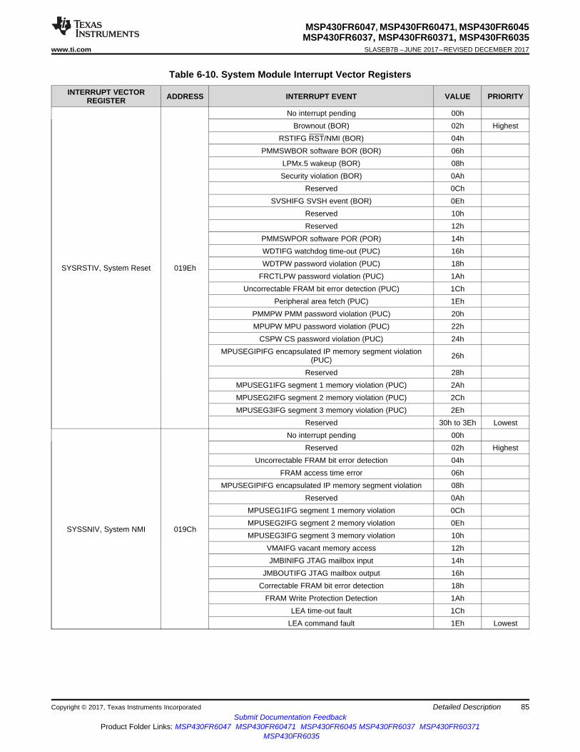
85
MSP430FR6047, MSP430FR60471, MSP430FR6045MSP430FR6037, MSP430FR60371, MSP430FR6035
www.ti.com SLASEB7B –JUNE 2017–REVISED DECEMBER 2017
Submit Documentation FeedbackProduct Folder Links: MSP430FR6047 MSP430FR60471 MSP430FR6045 MSP430FR6037 MSP430FR60371
MSP430FR6035
Detailed DescriptionCopyright © 2017, Texas Instruments Incorporated
Table 6-10. System Module Interrupt Vector Registers
INTERRUPT VECTORREGISTER ADDRESS INTERRUPT EVENT VALUE PRIORITY
SYSRSTIV, System Reset 019Eh
No interrupt pending 00hBrownout (BOR) 02h Highest
RSTIFG RST/NMI (BOR) 04hPMMSWBOR software BOR (BOR) 06h
LPMx.5 wakeup (BOR) 08hSecurity violation (BOR) 0Ah
Reserved 0ChSVSHIFG SVSH event (BOR) 0Eh
Reserved 10hReserved 12h
PMMSWPOR software POR (POR) 14hWDTIFG watchdog time-out (PUC) 16hWDTPW password violation (PUC) 18h
FRCTLPW password violation (PUC) 1AhUncorrectable FRAM bit error detection (PUC) 1Ch
Peripheral area fetch (PUC) 1EhPMMPW PMM password violation (PUC) 20hMPUPW MPU password violation (PUC) 22h
CSPW CS password violation (PUC) 24hMPUSEGIPIFG encapsulated IP memory segment violation
(PUC) 26h
Reserved 28hMPUSEG1IFG segment 1 memory violation (PUC) 2AhMPUSEG2IFG segment 2 memory violation (PUC) 2ChMPUSEG3IFG segment 3 memory violation (PUC) 2Eh
Reserved 30h to 3Eh Lowest
SYSSNIV, System NMI 019Ch
No interrupt pending 00hReserved 02h Highest
Uncorrectable FRAM bit error detection 04hFRAM access time error 06h
MPUSEGIPIFG encapsulated IP memory segment violation 08hReserved 0Ah
MPUSEG1IFG segment 1 memory violation 0ChMPUSEG2IFG segment 2 memory violation 0EhMPUSEG3IFG segment 3 memory violation 10h
VMAIFG vacant memory access 12hJMBINIFG JTAG mailbox input 14h
JMBOUTIFG JTAG mailbox output 16hCorrectable FRAM bit error detection 18h
FRAM Write Protection Detection 1AhLEA time-out fault 1Ch
LEA command fault 1Eh Lowest
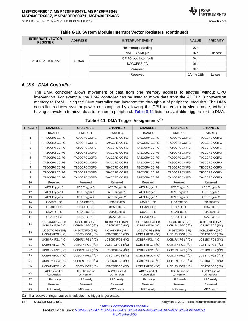
86
MSP430FR6047, MSP430FR60471, MSP430FR6045MSP430FR6037, MSP430FR60371, MSP430FR6035SLASEB7B –JUNE 2017–REVISED DECEMBER 2017 www.ti.com
Submit Documentation FeedbackProduct Folder Links: MSP430FR6047 MSP430FR60471 MSP430FR6045 MSP430FR6037 MSP430FR60371
MSP430FR6035
Detailed Description Copyright © 2017, Texas Instruments Incorporated
Table 6-10. System Module Interrupt Vector Registers (continued)INTERRUPT VECTOR
REGISTER ADDRESS INTERRUPT EVENT VALUE PRIORITY
SYSUNIV, User NMI 019Ah
No interrupt pending 00hNMIIFG NMI pin 02h Highest
OFIFG oscillator fault 04hDACCESSIFG 06h
Reserved 08hReserved 0Ah to 1Eh Lowest
(1) If a reserved trigger source is selected, no trigger is generated.
6.13.9 DMA ControllerThe DMA controller allows movement of data from one memory address to another without CPUintervention. For example, the DMA controller can be used to move data from the ADC12_B conversionmemory to RAM. Using the DMA controller can increase the throughput of peripheral modules. The DMAcontroller reduces system power consumption by allowing the CPU to remain in sleep mode, withouthaving to awaken to move data to or from a peripheral. Table 6-11 lists the available triggers for the DMA.
Table 6-11. DMA Trigger Assignments (1)
TRIGGER CHANNEL 0 CHANNEL 1 CHANNEL 2 CHANNEL 3 CHANNEL 4 CHANNEL 5
0 DMAREQ DMAREQ DMAREQ DMAREQ DMAREQ DMAREQ
1 TA0CCR0 CCIFG TA0CCR0 CCIFG TA0CCR0 CCIFG TA0CCR0 CCIFG TA0CCR0 CCIFG TA0CCR0 CCIFG
2 TA0CCR2 CCIFG TA0CCR2 CCIFG TA0CCR2 CCIFG TA0CCR2 CCIFG TA0CCR2 CCIFG TA0CCR2 CCIFG
3 TA1CCR0 CCIFG TA1CCR0 CCIFG TA1CCR0 CCIFG TA1CCR0 CCIFG TA1CCR0 CCIFG TA1CCR0 CCIFG
4 TA1CCR2 CCIFG TA1CCR2 CCIFG TA1CCR2 CCIFG TA1CCR2 CCIFG TA1CCR2 CCIFG TA1CCR2 CCIFG
5 TA2CCR0 CCIFG TA2CCR0 CCIFG TA2CCR0 CCIFG TA2CCR0 CCIFG TA2CCR0 CCIFG TA2CCR0 CCIFG
6 TA3CCR0 CCIFG TA3CCR0 CCIFG TA3CCR0 CCIFG TA3CCR0 CCIFG TA3CCR0 CCIFG TA3CCR0 CCIFG
7 TB0CCR0 CCIFG TB0CCR0 CCIFG TB0CCR0 CCIFG TB0CCR0 CCIFG TB0CCR0 CCIFG TB0CCR0 CCIFG
8 TB0CCR2 CCIFG TB0CCR2 CCIFG TB0CCR2 CCIFG TB0CCR2 CCIFG TB0CCR2 CCIFG TB0CCR2 CCIFG
9 TA4CCR0 CCIFG TA4CCR0 CCIFG TA4CCR0 CCIFG TA4CCR0 CCIFG TA4CCR0 CCIFG TA4CCR0 CCIFG
10 Reserved Reserved Reserved Reserved Reserved Reserved
11 AES Trigger 0 AES Trigger 0 AES Trigger 0 AES Trigger 0 AES Trigger 0 AES Trigger 0
12 AES Trigger 1 AES Trigger 1 AES Trigger 1 AES Trigger 1 AES Trigger 1 AES Trigger 1
13 AES Trigger 2 AES Trigger 2 AES Trigger 2 AES Trigger 2 AES Trigger 2 AES Trigger 2
14 UCA0RXIFG UCA0RXIFG UCA0RXIFG UCA2RXIFG UCA2RXIFG UCA2RXIFG
15 UCA0TXIFG UCA0TXIFG UCA0TXIFG UCA2TXIFG UCA2TXIFG UCA2TXIFG
16 UCA1RXIFG UCA1RXIFG UCA1RXIFG UCA3RXIFG UCA3RXIFG UCA3RXIFG
17 UCA1TXIFG UCA1TXIFG UCA1TXIFG UCA3TXIFG UCA3TXIFG UCA3TXIFG
18 UCB0RXIFG (SPI)UCB0RXIFG0 (I2C)
UCB0RXIFG (SPI)UCB0RXIFG0 (I2C)
UCB0RXIFG (SPI)UCB0RXIFG0 (I2C)
UCB1RXIFG (SPI)UCB1RXIFG0 (I2C)
UCB1RXIFG (SPI)UCB1RXIFG0 (I2C)
UCB1RXIFG (SPI)UCB1RXIFG0 (I2C)
19 UCB0TXIFG (SPI)UCB0TXIFG0 (I2C)
UCB0TXIFG (SPI)UCB0TXIFG0 (I2C)
UCB0TXIFG (SPI)UCB0TXIFG0 (I2C)
UCB1TXIFG (SPI)UCB1TXIFG0 (I2C)
UCB1TXIFG (SPI)UCB1TXIFG0 (I2C)
UCB1TXIFG (SPI)UCB1TXIFG0 (I2C)
20 UCB0RXIFG1 (I2C) UCB0RXIFG1 (I2C) UCB0RXIFG1 (I2C) UCB1RXIFG1 (I2C) UCB1RXIFG1 (I2C) UCB1RXIFG1 (I2C)
21 UCB0TXIFG1 (I2C) UCB0TXIFG1 (I2C) UCB0TXIFG1 (I2C) UCB1TXIFG1 (I2C) UCB1TXIFG1 (I2C) UCB1TXIFG1 (I2C)
22 UCB0RXIFG2 (I2C) UCB0RXIFG2 (I2C) UCB0RXIFG2 (I2C) UCB1RXIFG2 (I2C) UCB1RXIFG2 (I2C) UCB1RXIFG2 (I2C)
23 UCB0TXIFG2 (I2C) UCB0TXIFG2 (I2C) UCB0TXIFG2 (I2C) UCB1TXIFG2 (I2C) UCB1TXIFG2 (I2C) UCB1TXIFG2 (I2C)
24 UCB0RXIFG3 (I2C) UCB0RXIFG3 (I2C) UCB0RXIFG3 (I2C) UCB1RXIFG3 (I2C) UCB1RXIFG3 (I2C) UCB1RXIFG3 (I2C)
25 UCB0TXIFG3 (I2C) UCB0TXIFG3 (I2C) UCB0TXIFG3 (I2C) UCB1TXIFG3 (I2C) UCB1TXIFG3 (I2C) UCB1TXIFG3 (I2C)
26 ADC12 end ofconversion
ADC12 end ofconversion
ADC12 end ofconversion
ADC12 end ofconversion
ADC12 end ofconversion
ADC12 end ofconversion
27 LEA ready LEA ready LEA ready LEA ready LEA ready LEA ready
28 Reserved Reserved Reserved Reserved Reserved Reserved
29 MPY ready MPY ready MPY ready MPY ready MPY ready MPY ready

87
MSP430FR6047, MSP430FR60471, MSP430FR6045MSP430FR6037, MSP430FR60371, MSP430FR6035
www.ti.com SLASEB7B –JUNE 2017–REVISED DECEMBER 2017
Submit Documentation FeedbackProduct Folder Links: MSP430FR6047 MSP430FR60471 MSP430FR6045 MSP430FR6037 MSP430FR60371
MSP430FR6035
Detailed DescriptionCopyright © 2017, Texas Instruments Incorporated
Table 6-11. DMA Trigger Assignments(1) (continued)TRIGGER CHANNEL 0 CHANNEL 1 CHANNEL 2 CHANNEL 3 CHANNEL 4 CHANNEL 5
30 DMA2IFG DMA0IFG DMA1IFG DMA5IFG DMA3IFG DMA4IFG
31 DMAE0 DMAE0 DMAE0 DMAE0 DMAE0 DMAE0
(1) Only on devices with ADC.
6.13.10 Enhanced Universal Serial Communication Interface (eUSCI)The eUSCI modules are used for serial data communication. The eUSCI module supports synchronouscommunication protocols such as SPI (3- or 4-pin) and I2C, and asynchronous communication protocolssuch as UART, enhanced UART with automatic baud-rate detection, and IrDA.
The eUSCI_A0, eUSCI_A1, eUSCI_A2, and eUSCI_A3 modules support SPI (3- or 4-pin), UART,enhanced UART, and IrDA.
The eUSCI_B0 and eUSCI_B1 modules support SPI (3- or 4-pin) and I2C.
Four eUSCI_A modules and two eUSCI_B modules are implemented.
6.13.11 TA0, TA1, and TA4TA0, TA1, and TA4 are 16-bit timers and counters (Timer_A type) with three (TA0 and TA1) or two (TA4)capture/compare registers each. Each timer can support multiple captures or compares, PWM outputs,and interval timing (see Table 6-12, Table 6-13, and Table 6-14). Each timer has extensive interruptcapabilities. Interrupts may be generated from the counter on overflow conditions and from eachcapture/compare register.
Table 6-12. TA0 Signal Connections
INPUT PORT PIN DEVICE INPUTSIGNAL
MODULE INPUTSIGNAL
MODULEBLOCK
MODULEOUTPUTSIGNAL
DEVICEOUTPUTSIGNAL
OUTPUT PORT PIN
P2.4, P4.5, P5.5 TA0CLK TACLK
Timer N/A N/AACLK (internal) ACLK
SMCLK (internal) SMCLKP2.4. P4.5, P5.5 TA0CLK INCLK
P2.3 TA0.0 CCI0A
CCR0 TA0 TA0.0
P2.3P2.7 TA0.0 CCI0B P2.7
DVSS GNDDVCC VCC
P7.4 TA0.1 CCI1A
CCR1 TA1 TA0.1
P7.4
COUT (internal) CCI1B ADC12(internal) (1)
ADC12SHSx = 1DVSS GNDDVCC VCC
P7.7 TA0.2 CCI2A
CCR2 TA2 TA0.2
P7.7
ACLK (internal) CCI2B
UUPS Trigger(USSPWRUP)
UUPS.CTL.USSPWRUPSEL = 2
DVSS GNDDVCC VCC
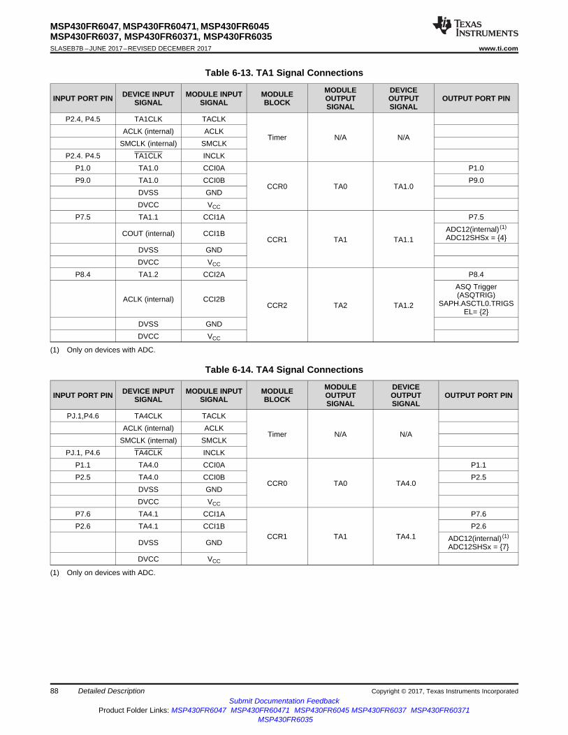
88
MSP430FR6047, MSP430FR60471, MSP430FR6045MSP430FR6037, MSP430FR60371, MSP430FR6035SLASEB7B –JUNE 2017–REVISED DECEMBER 2017 www.ti.com
Submit Documentation FeedbackProduct Folder Links: MSP430FR6047 MSP430FR60471 MSP430FR6045 MSP430FR6037 MSP430FR60371
MSP430FR6035
Detailed Description Copyright © 2017, Texas Instruments Incorporated
(1) Only on devices with ADC.
Table 6-13. TA1 Signal Connections
INPUT PORT PIN DEVICE INPUTSIGNAL
MODULE INPUTSIGNAL
MODULEBLOCK
MODULEOUTPUTSIGNAL
DEVICEOUTPUTSIGNAL
OUTPUT PORT PIN
P2.4, P4.5 TA1CLK TACLK
Timer N/A N/AACLK (internal) ACLK
SMCLK (internal) SMCLKP2.4. P4.5 TA1CLK INCLK
P1.0 TA1.0 CCI0A
CCR0 TA0 TA1.0
P1.0P9.0 TA1.0 CCI0B P9.0
DVSS GNDDVCC VCC
P7.5 TA1.1 CCI1A
CCR1 TA1 TA1.1
P7.5
COUT (internal) CCI1B ADC12(internal) (1)
ADC12SHSx = 4DVSS GNDDVCC VCC
P8.4 TA1.2 CCI2A
CCR2 TA2 TA1.2
P8.4
ACLK (internal) CCI2B
ASQ Trigger(ASQTRIG)
SAPH.ASCTL0.TRIGSEL= 2
DVSS GNDDVCC VCC
(1) Only on devices with ADC.
Table 6-14. TA4 Signal Connections
INPUT PORT PIN DEVICE INPUTSIGNAL
MODULE INPUTSIGNAL
MODULEBLOCK
MODULEOUTPUTSIGNAL
DEVICEOUTPUTSIGNAL
OUTPUT PORT PIN
PJ.1,P4.6 TA4CLK TACLK
Timer N/A N/AACLK (internal) ACLK
SMCLK (internal) SMCLKPJ.1, P4.6 TA4CLK INCLK
P1.1 TA4.0 CCI0A
CCR0 TA0 TA4.0
P1.1P2.5 TA4.0 CCI0B P2.5
DVSS GNDDVCC VCC
P7.6 TA4.1 CCI1A
CCR1 TA1 TA4.1
P7.6P2.6 TA4.1 CCI1B P2.6
DVSS GND ADC12(internal) (1)
ADC12SHSx = 7DVCC VCC
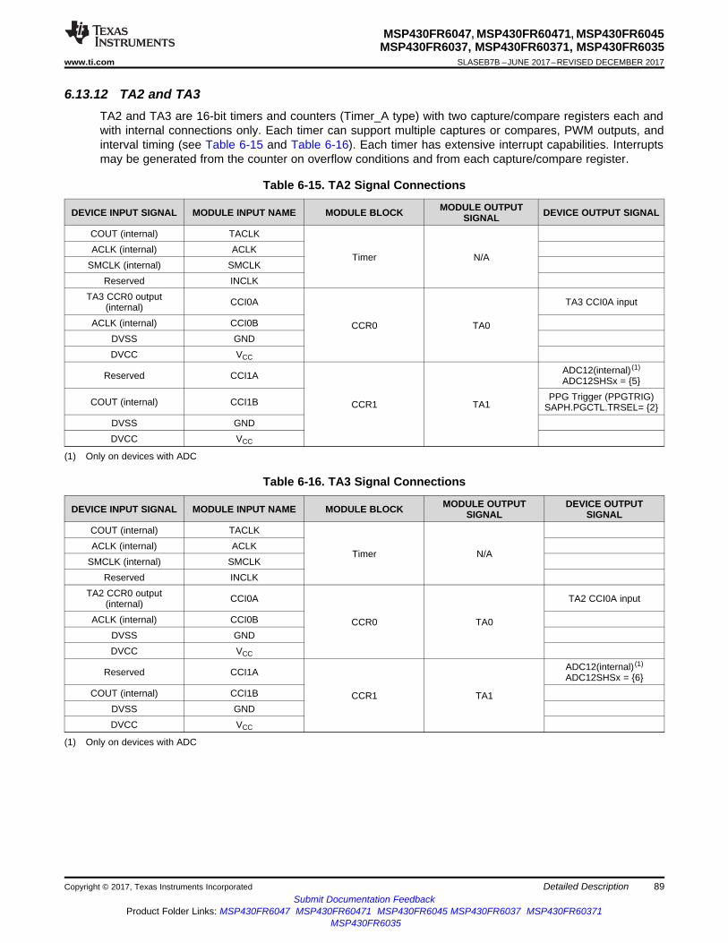
89
MSP430FR6047, MSP430FR60471, MSP430FR6045MSP430FR6037, MSP430FR60371, MSP430FR6035
www.ti.com SLASEB7B –JUNE 2017–REVISED DECEMBER 2017
Submit Documentation FeedbackProduct Folder Links: MSP430FR6047 MSP430FR60471 MSP430FR6045 MSP430FR6037 MSP430FR60371
MSP430FR6035
Detailed DescriptionCopyright © 2017, Texas Instruments Incorporated
(1) Only on devices with ADC
6.13.12 TA2 and TA3TA2 and TA3 are 16-bit timers and counters (Timer_A type) with two capture/compare registers each andwith internal connections only. Each timer can support multiple captures or compares, PWM outputs, andinterval timing (see Table 6-15 and Table 6-16). Each timer has extensive interrupt capabilities. Interruptsmay be generated from the counter on overflow conditions and from each capture/compare register.
Table 6-15. TA2 Signal Connections
DEVICE INPUT SIGNAL MODULE INPUT NAME MODULE BLOCK MODULE OUTPUTSIGNAL DEVICE OUTPUT SIGNAL
COUT (internal) TACLK
Timer N/AACLK (internal) ACLK
SMCLK (internal) SMCLKReserved INCLK
TA3 CCR0 output(internal) CCI0A
CCR0 TA0
TA3 CCI0A input
ACLK (internal) CCI0BDVSS GNDDVCC VCC
Reserved CCI1A
CCR1 TA1
ADC12(internal) (1)
ADC12SHSx = 5
COUT (internal) CCI1B PPG Trigger (PPGTRIG)SAPH.PGCTL.TRSEL= 2
DVSS GNDDVCC VCC
(1) Only on devices with ADC
Table 6-16. TA3 Signal Connections
DEVICE INPUT SIGNAL MODULE INPUT NAME MODULE BLOCK MODULE OUTPUTSIGNAL
DEVICE OUTPUTSIGNAL
COUT (internal) TACLK
Timer N/AACLK (internal) ACLK
SMCLK (internal) SMCLKReserved INCLK
TA2 CCR0 output(internal) CCI0A
CCR0 TA0
TA2 CCI0A input
ACLK (internal) CCI0BDVSS GNDDVCC VCC
Reserved CCI1A
CCR1 TA1
ADC12(internal) (1)
ADC12SHSx = 6COUT (internal) CCI1B
DVSS GNDDVCC VCC
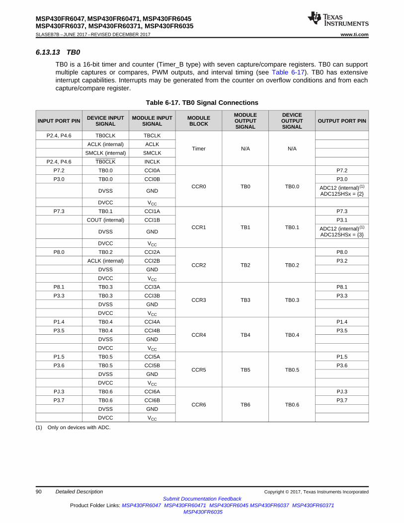
90
MSP430FR6047, MSP430FR60471, MSP430FR6045MSP430FR6037, MSP430FR60371, MSP430FR6035SLASEB7B –JUNE 2017–REVISED DECEMBER 2017 www.ti.com
Submit Documentation FeedbackProduct Folder Links: MSP430FR6047 MSP430FR60471 MSP430FR6045 MSP430FR6037 MSP430FR60371
MSP430FR6035
Detailed Description Copyright © 2017, Texas Instruments Incorporated
(1) Only on devices with ADC.
6.13.13 TB0TB0 is a 16-bit timer and counter (Timer_B type) with seven capture/compare registers. TB0 can supportmultiple captures or compares, PWM outputs, and interval timing (see Table 6-17). TB0 has extensiveinterrupt capabilities. Interrupts may be generated from the counter on overflow conditions and from eachcapture/compare register.
Table 6-17. TB0 Signal Connections
INPUT PORT PIN DEVICE INPUTSIGNAL
MODULE INPUTSIGNAL
MODULEBLOCK
MODULEOUTPUTSIGNAL
DEVICEOUTPUTSIGNAL
OUTPUT PORT PIN
P2.4, P4.6 TB0CLK TBCLK
Timer N/A N/AACLK (internal) ACLK
SMCLK (internal) SMCLKP2.4, P4.6 TB0CLK INCLK
P7.2 TB0.0 CCI0A
CCR0 TB0 TB0.0
P7.2P3.0 TB0.0 CCI0B P3.0
DVSS GND ADC12 (internal) (1)
ADC12SHSx = 2DVCC VCC
P7.3 TB0.1 CCI1A
CCR1 TB1 TB0.1
P7.3COUT (internal) CCI1B P3.1
DVSS GND ADC12 (internal) (1)
ADC12SHSx = 3DVCC VCC
P8.0 TB0.2 CCI2A
CCR2 TB2 TB0.2
P8.0ACLK (internal) CCI2B P3.2
DVSS GNDDVCC VCC
P8.1 TB0.3 CCI3A
CCR3 TB3 TB0.3
P8.1P3.3 TB0.3 CCI3B P3.3
DVSS GNDDVCC VCC
P1.4 TB0.4 CCI4A
CCR4 TB4 TB0.4
P1.4P3.5 TB0.4 CCI4B P3.5
DVSS GNDDVCC VCC
P1.5 TB0.5 CCI5A
CCR5 TB5 TB0.5
P1.5P3.6 TB0.5 CCI5B P3.6
DVSS GNDDVCC VCC
PJ.3 TB0.6 CCI6A
CCR6 TB6 TB0.6
PJ.3P3.7 TB0.6 CCI6B P3.7
DVSS GNDDVCC VCC
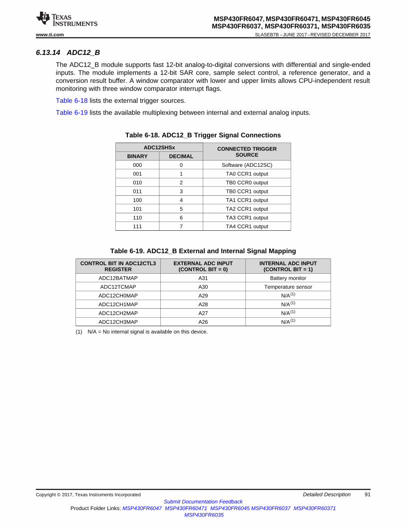
91
MSP430FR6047, MSP430FR60471, MSP430FR6045MSP430FR6037, MSP430FR60371, MSP430FR6035
www.ti.com SLASEB7B –JUNE 2017–REVISED DECEMBER 2017
Submit Documentation FeedbackProduct Folder Links: MSP430FR6047 MSP430FR60471 MSP430FR6045 MSP430FR6037 MSP430FR60371
MSP430FR6035
Detailed DescriptionCopyright © 2017, Texas Instruments Incorporated
6.13.14 ADC12_BThe ADC12_B module supports fast 12-bit analog-to-digital conversions with differential and single-endedinputs. The module implements a 12-bit SAR core, sample select control, a reference generator, and aconversion result buffer. A window comparator with lower and upper limits allows CPU-independent resultmonitoring with three window comparator interrupt flags.
Table 6-18 lists the external trigger sources.
Table 6-19 lists the available multiplexing between internal and external analog inputs.
Table 6-18. ADC12_B Trigger Signal Connections
ADC12SHSx CONNECTED TRIGGERSOURCEBINARY DECIMAL
000 0 Software (ADC12SC)001 1 TA0 CCR1 output010 2 TB0 CCR0 output011 3 TB0 CCR1 output100 4 TA1 CCR1 output101 5 TA2 CCR1 output110 6 TA3 CCR1 output111 7 TA4 CCR1 output
(1) N/A = No internal signal is available on this device.
Table 6-19. ADC12_B External and Internal Signal Mapping
CONTROL BIT IN ADC12CTL3REGISTER
EXTERNAL ADC INPUT(CONTROL BIT = 0)
INTERNAL ADC INPUT(CONTROL BIT = 1)
ADC12BATMAP A31 Battery monitorADC12TCMAP A30 Temperature sensor
ADC12CH0MAP A29 N/A (1)
ADC12CH1MAP A28 N/A (1)
ADC12CH2MAP A27 N/A (1)
ADC12CH3MAP A26 N/A (1)

92
MSP430FR6047, MSP430FR60471, MSP430FR6045MSP430FR6037, MSP430FR60371, MSP430FR6035SLASEB7B –JUNE 2017–REVISED DECEMBER 2017 www.ti.com
Submit Documentation FeedbackProduct Folder Links: MSP430FR6047 MSP430FR60471 MSP430FR6045 MSP430FR6037 MSP430FR60371
MSP430FR6035
Detailed Description Copyright © 2017, Texas Instruments Incorporated
6.13.15 USSTable 6-20 lists the available UUPS triggers.
Table 6-20. UUPS Trigger Signal Connections
UUPS.CTL.USSPWRUPSELCONNECTED TRIGGER SOURCE
BINARY00 Software (UUPS.CTL.USSPWRUP)01 RTC (any enabled interrupt events)10 TA0 CCR2 output11 P1.7
Table 6-21 lists the available PPG triggers.
Table 6-21. PPG Trigger Signal Connections
SAPH.PGCTL.TRSELCONNECTED TRIGGER SOURCE
BINARY00 Software (SAPH.PPGTRIG.PPGTRIG)01 ASQ (Acquisition Sequencer)10 TA2 CCR1 output11 Reserved
Table 6-22 lists the available ASQ triggers.
Table 6-22. ASQ Trigger Signal Connections
SAPH.ASCTL0.TRIGSELCONNECTED TRIGGER SOURCE
BINARY00 Software (SAPH.ASQTRIG.ASQTRIG)01 PSQ (Power Sequencer)10 TA1 CCR2 output11 Reserved
6.13.16 Comparator_EThe primary function of the Comparator_E module is to support precision slope analog-to-digitalconversions, battery voltage supervision, and monitoring of external analog signals.
6.13.17 CRC16The CRC16 module produces a signature based on a sequence of entered data values and can be usedfor data checking purposes. The CRC16 module signature is based on the CRC-CCITT standard.
6.13.18 CRC32The CRC32 module produces a signature based on a sequence of entered data values and can be usedfor data checking purposes. The CRC32 module signature is based on the ISO 3309 standard.
6.13.19 AES256 AcceleratorThe AES accelerator module performs encryption and decryption of 128-bit data with 128-, 192-, or 256-bit keys according to the Advanced Encryption Standard (AES) (FIPS PUB 197) in hardware.

93
MSP430FR6047, MSP430FR60471, MSP430FR6045MSP430FR6037, MSP430FR60371, MSP430FR6035
www.ti.com SLASEB7B –JUNE 2017–REVISED DECEMBER 2017
Submit Documentation FeedbackProduct Folder Links: MSP430FR6047 MSP430FR60471 MSP430FR6045 MSP430FR6037 MSP430FR60371
MSP430FR6035
Detailed DescriptionCopyright © 2017, Texas Instruments Incorporated
6.13.20 True Random SeedThe device descriptor information (TLV) section contains a 128-bit true random seed that can be used toimplement a deterministic random number generator.
6.13.21 Shared Reference (REF)The REF module generates critical reference voltages that can be used by the various analog peripheralsin the device.
6.13.22 LCD_CThe LCD_C driver generates the segment and common signals required to drive a liquid crystal display(LCD). The LCD_C controller has dedicated data memories to hold segment drive information. Commonand segment signals are generated as defined by the mode. Static and 2-mux to 8-mux LCDs aresupported. The module can provide an LCD voltage independent of the supply voltage with its integratedcharge pump. It is possible to control the level of the LCD voltage and thus contrast by software. Themodule also provides an automatic blinking capability for individual segments in static, 2-, 3-, and 4-muxmodes.
To reduce system noise, the charge pump can be temporarily disabled. Table 6-23 lists the availableautomatic charge pump disable options.
Table 6-23. LCD Automatic Charge Pump Disable Bits (LCDCPDISx)
CONTROL BIT DESCRIPTION
LCDCPDIS0LCD charge pump disable during ADC12 conversion0b = LCD charge pump not automatically disabled during conversion.1b = LCD charge pump automatically disabled during conversion.
LCDCPDIS1 to LCDCPDIS7 No functionality.
6.13.23 Embedded Emulation
6.13.23.1 Embedded Emulation Module (EEM) (S Version)
The EEM supports real-time in-system debugging. The S version of the EEM has the following features:• Three hardware triggers or breakpoints on memory access• One hardware trigger or breakpoint on CPU register write access• Up to four hardware triggers that can be combined to form complex triggers or breakpoints• One cycle counter• Clock control on module level
6.13.23.2 EnergyTrace++ Technology
The devices implement circuitry to support EnergyTrace++ technology. The EnergyTrace++ technologylets the user observe information about the internal states of the microcontroller. These states include theCPU Program Counter (PC), the on or off status of the peripherals and system clocks (regardless of theclock source), and the low-power mode currently in use. These states can always be read by a debugtool, even when the microcontroller sleeps in LPMx.5 modes.
The activity of the following modules can be observed:• LEA is running• MPY is calculating.• WDT is counting.• RTC is counting.• ADC: a sequence, sample, or conversion is active.• REF: REFBG or REFGEN active and BG in static mode.

94
MSP430FR6047, MSP430FR60471, MSP430FR6045MSP430FR6037, MSP430FR60371, MSP430FR6035SLASEB7B –JUNE 2017–REVISED DECEMBER 2017 www.ti.com
Submit Documentation FeedbackProduct Folder Links: MSP430FR6047 MSP430FR60471 MSP430FR6045 MSP430FR6037 MSP430FR60371
MSP430FR6035
Detailed Description Copyright © 2017, Texas Instruments Incorporated
• COMP is on.• AES is encrypting or decrypting.• eUSCI_A0 is transferring (receiving or transmitting) data.• eUSCI_A1 is transferring (receiving or transmitting) data.• eUSCI_A2 is transferring (receiving or transmitting) data.• eUSCI_A3 is transferring (receiving or transmitting) data.• eUSCI_B0 is transferring (receiving or transmitting) data.• eUSCI_B1 is transferring (receiving or transmitting) data.• TB0 is counting.• TA0 is counting.• TA1 is counting.• TA2 is counting.• TA3 is counting.• TA4 is counting.• LCD_C is running.• USS status

95
MSP430FR6047, MSP430FR60471, MSP430FR6045MSP430FR6037, MSP430FR60371, MSP430FR6035
www.ti.com SLASEB7B –JUNE 2017–REVISED DECEMBER 2017
Submit Documentation FeedbackProduct Folder Links: MSP430FR6047 MSP430FR60471 MSP430FR6045 MSP430FR6037 MSP430FR60371
MSP430FR6035
Detailed DescriptionCopyright © 2017, Texas Instruments Incorporated
6.14 Input/Output Diagrams
6.14.1 Port Function Select Registers (PySEL1 , PySEL0)Port pins are multiplexed with peripheral module functions as described in the MSP430FR58xx,MSP430FR59xx, and MSP430FR6xx Family User's Guide. The functions of each port pin are controlledby its port function select registers, PySEL1 and PySEL0, where y = port number. The bits in the registersare mapped to the pins in the port. The primary module function, secondary module function, and tertiarymodule function of the pins are determined by the configuration of the PySEL1.x and PySEL0.x bits (seeTable 6-24). For example, P1SEL1.0 and P1SEL0.0 determine the primary module function, secondarymodule function, and tertiary module function of the P1.0 pin, which is in port 1. The module functions mayalso require the PxDIR bits to be configured according to the direction needed for the module function.
Table 6-24. I/O Function Selection
I/O FUNCTIONS PySEL1.x PySEL1.xGeneral-purpose I/O is selected 0 0Primary module function is selected 0 1Secondary module function is selected 1 0Tertiary module function is selected 1 1
See the port pin function tables in the following sections for the configurations of the function and directionfor each pin.

PxSEL1.x
PxDIR.x
PxIN.x
EN
To modules
PxOUT.x
1
0DVSS
DVCC 1
D
To Comparator
From Comparator
Pad Logic
To ADC
From ADC
BusKeeper
Direction0: Input1: Output
CBPD.x
PxREN.x
0 1
0 0
1 0
1 1
PxSEL0.x
0 1
0 0
1 0
1 1
(ADC) Reference
module 1 or DVSS
module 2 or DVSS
module 3 or DVSS
module 1 or PxDIR.x
module 2 or PxDIR.x
module 3 or PxDIR.x
96
MSP430FR6047, MSP430FR60471, MSP430FR6045MSP430FR6037, MSP430FR60371, MSP430FR6035SLASEB7B –JUNE 2017–REVISED DECEMBER 2017 www.ti.com
Submit Documentation FeedbackProduct Folder Links: MSP430FR6047 MSP430FR60471 MSP430FR6045 MSP430FR6037 MSP430FR60371
MSP430FR6035
Detailed Description Copyright © 2017, Texas Instruments Incorporated
6.14.2 Port P1 (P1.0 and P1.1) Input/Output With Schmitt TriggerFigure 6-3 shows the port diagram. Table 6-25 summarizes the selection of the pin function.
NOTE: Functional representation only.
Figure 6-3. Port P1 (P1.0 to P1.1) Diagram

97
MSP430FR6047, MSP430FR60471, MSP430FR6045MSP430FR6037, MSP430FR60371, MSP430FR6035
www.ti.com SLASEB7B –JUNE 2017–REVISED DECEMBER 2017
Submit Documentation FeedbackProduct Folder Links: MSP430FR6047 MSP430FR60471 MSP430FR6045 MSP430FR6037 MSP430FR60371
MSP430FR6035
Detailed DescriptionCopyright © 2017, Texas Instruments Incorporated
(1) X = Don't care(2) Direction controlled by eUSCI_A1 module.(3) Setting P1SEL1.x and P1SEL0.x disables the output driver and the input Schmitt trigger to prevent parasitic cross currents when
applying analog signals.(4) Setting the CEPDx bit of the comparator disables the output driver and the input Schmitt trigger to prevent parasitic cross currents when
applying analog signals. Selecting the Cx input pin to the comparator multiplexer with the input select bits in the comparator moduleautomatically disables output driver and input buffer for that pin, regardless of the state of the associated CEPDx bit.
Table 6-25. Port P1 (P1.0 to P1.1) Pin Functions
PIN NAME (P1.x) x FUNCTIONCONTROL BITS AND SIGNALS (1)
P1DIR.x P1SEL1.x P1SEL0.x
P1.0/UCA1CLK/TA1.0/A0/C0/ VREF-/VeREF- 0
P1.0 (I/O) I: 0; O: 1 0 0UCA1CLK X (2) 0 1TA1.CCI0A 0
1 0TA1.0 1A0, C0, VREF-, VeREF- (3) (4) X 1 1
P1.1/UCA1STE/TA4.0/A1/C1/VREF+/VeREF+ 1
P1.1 (I/O) I: 0; O: 1 0 0UCA1STE X (2) 0 1TA4.CCI0A 0
1 0TA4.0 1A1, C1, VREF+, VeREF+ (3) (4) X 1 1
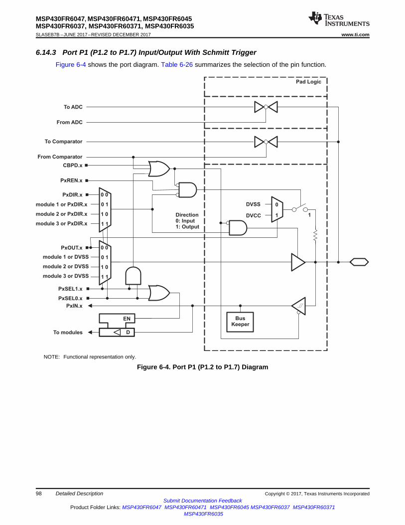
PxSEL1.x
PxDIR.x
PxIN.x
EN
To modules
PxOUT.x
1
0DVSS
DVCC 1
D
To Comparator
From Comparator
Pad Logic
To ADC
From ADC
BusKeeper
Direction0: Input1: Output
CBPD.x
PxREN.x
0 1
0 0
1 0
1 1
PxSEL0.x
0 1
0 0
1 0
1 1
module 1 or DVSS
module 2 or DVSS
module 3 or DVSS
module 1 or PxDIR.x
module 2 or PxDIR.x
module 3 or PxDIR.x
98
MSP430FR6047, MSP430FR60471, MSP430FR6045MSP430FR6037, MSP430FR60371, MSP430FR6035SLASEB7B –JUNE 2017–REVISED DECEMBER 2017 www.ti.com
Submit Documentation FeedbackProduct Folder Links: MSP430FR6047 MSP430FR60471 MSP430FR6045 MSP430FR6037 MSP430FR60371
MSP430FR6035
Detailed Description Copyright © 2017, Texas Instruments Incorporated
6.14.3 Port P1 (P1.2 to P1.7) Input/Output With Schmitt TriggerFigure 6-4 shows the port diagram. Table 6-26 summarizes the selection of the pin function.
NOTE: Functional representation only.
Figure 6-4. Port P1 (P1.2 to P1.7) Diagram

99
MSP430FR6047, MSP430FR60471, MSP430FR6045MSP430FR6037, MSP430FR60371, MSP430FR6035
www.ti.com SLASEB7B –JUNE 2017–REVISED DECEMBER 2017
Submit Documentation FeedbackProduct Folder Links: MSP430FR6047 MSP430FR60471 MSP430FR6045 MSP430FR6037 MSP430FR60371
MSP430FR6035
Detailed DescriptionCopyright © 2017, Texas Instruments Incorporated
(1) X = Don't care(2) Direction controlled by eUSCI_A1 module.(3) Setting P1SEL1.x and P1SEL0.x disables the output driver and the input Schmitt trigger to prevent parasitic cross currents when
applying analog signals.(4) Setting the CEPDx bit of the comparator disables the output driver and the input Schmitt trigger to prevent parasitic cross currents when
applying analog signals. Selecting the Cx input pin to the comparator multiplexer with the input select bits in the comparator moduleautomatically disables output driver and input buffer for that pin, regardless of the state of the associated CEPDx bit.
(5) Direction controlled by eUSCI_B0 module.
Table 6-26. Port P1 (P1.2 to P1.7) Pin Functions
PIN NAME (P1.x) x FUNCTIONCONTROL BITS AND SIGNALS (1)
P1DIR.x P1SEL1.x P1SEL0.x
P1.2/UCA1SIMO/UCA1TXD/A8/C8 2
P1.2 (I/O) I: 0; O: 1 0 0UCA1SIMO/UCA1TXD X (2) 0 1N/A 0
1 0Internally tied to DVSS 1A8, C8 (3) (4) X 1 1
P1.3/UCA1SOMI/UCA1RXD/A9/C9 3
P1.3 (I/O) I: 0; O: 1 0 0UCA1SOMI/UCA1RXD X (2) 0 1N/A 0
1 0Internally tied to DVSS 1A9, C9 (3) (4) X 1 1
P1.4/TB0.4/UCB0STE/A2/C2 4
P1.4 (I/O) I: 0; O: 1 0 0TB0.CCI4A 0
0 1TB0.4 1UCB0STE X (5) 1 0A2, C2 (3) (4) X 1 1
P1.5/TB0.5/UCB0CLK/A3/C3 5
P1.5(I/O) I: 0; O: 1 0 0TB0.CCI5A 0
0 1TB0.5 1UCB0CLK X (5) 1 0A3, C3 (3) (4) X 1 1
P1.6/UCB0SIMO/UCB0SDA/A4/C4 6
P1.6(I/O) I: 0; O: 1 0 0N/A 0
0 1Internally tied to DVSS 1UCB0SIMO/UCB0SDA X (5) 1 0A4, C4 (3) (4) X 1 1
P1.7/USSTRG/UCB0SOMI/UCB0SCL/A5/C5 7
P1.7(I/O) I: 0; O: 1 0 0
USSTRG (independent function) 0X 11 X
Internally tied to DVSS 1 0 1UCB0SOMI/UCB0SCL X (5) 1 0A5, C5 (3) (4) X 1 1

PxSEL1.x
PxDIR.x
PxIN.x
EN
To modules
PxOUT.x
1
0DVSS
DVCC 1
D
To Comparator
From Comparator
Pad Logic
To ADC
From ADC
BusKeeper
Direction0: Input1: Output
CBPD.x
PxREN.x
0 1
0 0
1 0
1 1
PxSEL0.x
0 1
0 0
1 0
1 1
module 1 or DVSS
module 2 or DVSS
module 3 or DVSS
module 1 or PxDIR.x
module 2 or PxDIR.x
module 3 or PxDIR.x
100
MSP430FR6047, MSP430FR60471, MSP430FR6045MSP430FR6037, MSP430FR60371, MSP430FR6035SLASEB7B –JUNE 2017–REVISED DECEMBER 2017 www.ti.com
Submit Documentation FeedbackProduct Folder Links: MSP430FR6047 MSP430FR60471 MSP430FR6045 MSP430FR6037 MSP430FR60371
MSP430FR6035
Detailed Description Copyright © 2017, Texas Instruments Incorporated
6.14.4 Port P2 (P2.0 to P2.3) Input/Output With Schmitt TriggerFigure 6-5 shows the port diagram. Table 6-27 summarizes the selection of the pin function.
NOTE: Functional representation only.
Figure 6-5. Port P2 (P2.0 to P2.3) Diagram

101
MSP430FR6047, MSP430FR60471, MSP430FR6045MSP430FR6037, MSP430FR60371, MSP430FR6035
www.ti.com SLASEB7B –JUNE 2017–REVISED DECEMBER 2017
Submit Documentation FeedbackProduct Folder Links: MSP430FR6047 MSP430FR60471 MSP430FR6045 MSP430FR6037 MSP430FR60371
MSP430FR6035
Detailed DescriptionCopyright © 2017, Texas Instruments Incorporated
(1) X = Don't care(2) Direction controlled by eUSCI_A0 module.(3) Setting P2SEL1.x and P2SEL0.x disables the output driver and the input Schmitt trigger to prevent parasitic cross currents when
applying analog signals.(4) Setting the CEPDx bit of the comparator disables the output driver and the input Schmitt trigger to prevent parasitic cross currents when
applying analog signals. Selecting the Cx input pin to the comparator multiplexer with the input select bits in the comparator moduleautomatically disables output driver and input buffer for that pin, regardless of the state of the associated CEPDx bit.
Table 6-27. Port P2 (P2.0 to P2.3) Pin Functions
PIN NAME (P2.x) x FUNCTIONCONTROL BITS AND SIGNALS (1)
P2DIR.x P2SEL1.x P2SEL0.x
P2.0/UCA0SIMO/UCA0TXD/A6/C6 0
P2.0 (I/O) I: 0; O: 1 0 0N/A 0
0 1Internally tied to DVSS 1UCA0SIMO/UCA0TXD X (2) 1 0A6, C6 (3) (4) X 1 1
P2.1/UCA0SOMI/UCA0RXD/A7/C7 1
P2.1 (I/O) I: 0; O: 1 0 0N/A 0
0 1Internally tied to DVSS 1UCA0SOMI/UCA0RXD X (2) 1 0A7, C7 (3) (4) X 1 1
P2.2/COUT/UCA0CLK/A14/C14 2
P2.2 (I/O) I: 0; O: 1 0 0N/A 0
0 1COUT 1UCA0CLK X (2) 1 0A14, C14 (3) (4) X 1 1
P2.3/TA0.0/UCA0STE/A15/C15 3
P2.3(I/O) I: 0; O: 1 0 0TA0.CCI0A 0
0 1TA0.0 1UCA0STE X (2) 1 0A15, C15 (3) (4) X 1 1

PxSEL1.x
PxDIR.x
PxIN.x
EN
To modules
PxOUT.x
1
0DVSS
DVCC 1
D
Pad Logic
Sz
LCDSz
BusKeeper
Direction0: Input1: Output
PxREN.x
0 1
0 0
1 0
1 1
PxSEL0.x
0 1
0 0
1 0
1 1
module 1 or DVSS
module 2 or DVSS
module 3 or DVSS
module 1 or PxDIR.x
module 2 or PxDIR.x
module 3 or PxDIR.x
102
MSP430FR6047, MSP430FR60471, MSP430FR6045MSP430FR6037, MSP430FR60371, MSP430FR6035SLASEB7B –JUNE 2017–REVISED DECEMBER 2017 www.ti.com
Submit Documentation FeedbackProduct Folder Links: MSP430FR6047 MSP430FR60471 MSP430FR6045 MSP430FR6037 MSP430FR60371
MSP430FR6035
Detailed Description Copyright © 2017, Texas Instruments Incorporated
6.14.5 Port P2 (P2.4 to P2.7) Input/Output With Schmitt TriggerFigure 6-6 shows the port diagram. Table 6-28 summarizes the selection of the pin function.
NOTE: Functional representation only.
Figure 6-6. Port P2 (P2.4 to P2.7) Diagram
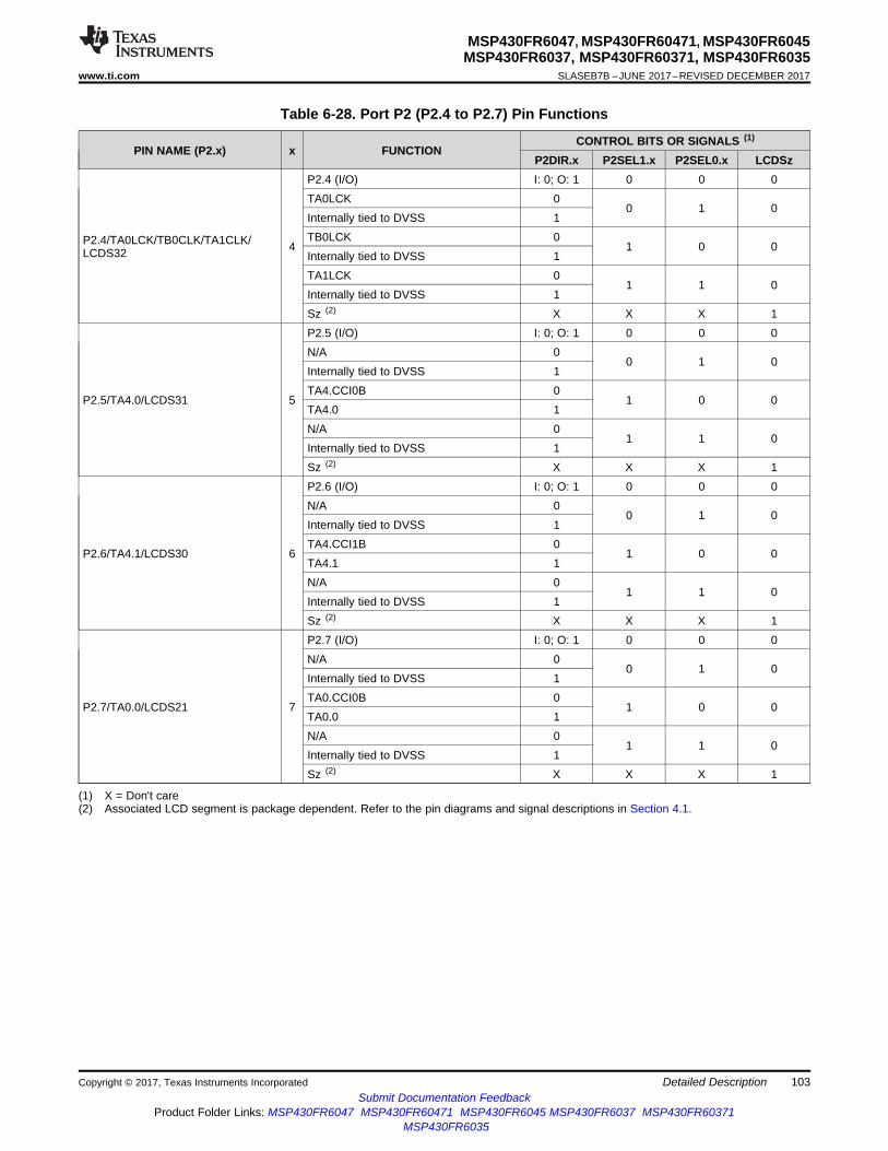
103
MSP430FR6047, MSP430FR60471, MSP430FR6045MSP430FR6037, MSP430FR60371, MSP430FR6035
www.ti.com SLASEB7B –JUNE 2017–REVISED DECEMBER 2017
Submit Documentation FeedbackProduct Folder Links: MSP430FR6047 MSP430FR60471 MSP430FR6045 MSP430FR6037 MSP430FR60371
MSP430FR6035
Detailed DescriptionCopyright © 2017, Texas Instruments Incorporated
(1) X = Don't care(2) Associated LCD segment is package dependent. Refer to the pin diagrams and signal descriptions in Section 4.1.
Table 6-28. Port P2 (P2.4 to P2.7) Pin Functions
PIN NAME (P2.x) x FUNCTIONCONTROL BITS OR SIGNALS (1)
P2DIR.x P2SEL1.x P2SEL0.x LCDSz
P2.4/TA0LCK/TB0CLK/TA1CLK/LCDS32 4
P2.4 (I/O) I: 0; O: 1 0 0 0TA0LCK 0
0 1 0Internally tied to DVSS 1TB0LCK 0
1 0 0Internally tied to DVSS 1TA1LCK 0
1 1 0Internally tied to DVSS 1Sz (2) X X X 1
P2.5/TA4.0/LCDS31 5
P2.5 (I/O) I: 0; O: 1 0 0 0N/A 0
0 1 0Internally tied to DVSS 1TA4.CCI0B 0
1 0 0TA4.0 1N/A 0
1 1 0Internally tied to DVSS 1Sz (2) X X X 1
P2.6/TA4.1/LCDS30 6
P2.6 (I/O) I: 0; O: 1 0 0 0N/A 0
0 1 0Internally tied to DVSS 1TA4.CCI1B 0
1 0 0TA4.1 1N/A 0
1 1 0Internally tied to DVSS 1Sz (2) X X X 1
P2.7/TA0.0/LCDS21 7
P2.7 (I/O) I: 0; O: 1 0 0 0N/A 0
0 1 0Internally tied to DVSS 1TA0.CCI0B 0
1 0 0TA0.0 1N/A 0
1 1 0Internally tied to DVSS 1Sz (2) X X X 1

PxSEL1.x
PxDIR.x
PxIN.x
EN
To modules
PxOUT.x
1
0DVSS
DVCC 1
D
Pad Logic
Sz
LCDSz
BusKeeper
Direction0: Input1: Output
PxREN.x
0 1
0 0
1 0
1 1
PxSEL0.x
0 1
0 0
1 0
1 1
module 1 or DVSS
module 2 or DVSS
module 3 or DVSS
module 1 or PxDIR.x
module 2 or PxDIR.x
module 3 or PxDIR.x
104
MSP430FR6047, MSP430FR60471, MSP430FR6045MSP430FR6037, MSP430FR60371, MSP430FR6035SLASEB7B –JUNE 2017–REVISED DECEMBER 2017 www.ti.com
Submit Documentation FeedbackProduct Folder Links: MSP430FR6047 MSP430FR60471 MSP430FR6045 MSP430FR6037 MSP430FR60371
MSP430FR6035
Detailed Description Copyright © 2017, Texas Instruments Incorporated
6.14.6 Port P3 (P3.0 to P3.7) Input/Output With Schmitt TriggerFigure 6-7 shows the port diagram. Table 6-29 summarizes the selection of the pin function.
NOTE: Functional representation only.
Figure 6-7. Port P3 (P3.0 to P3.7) Diagram
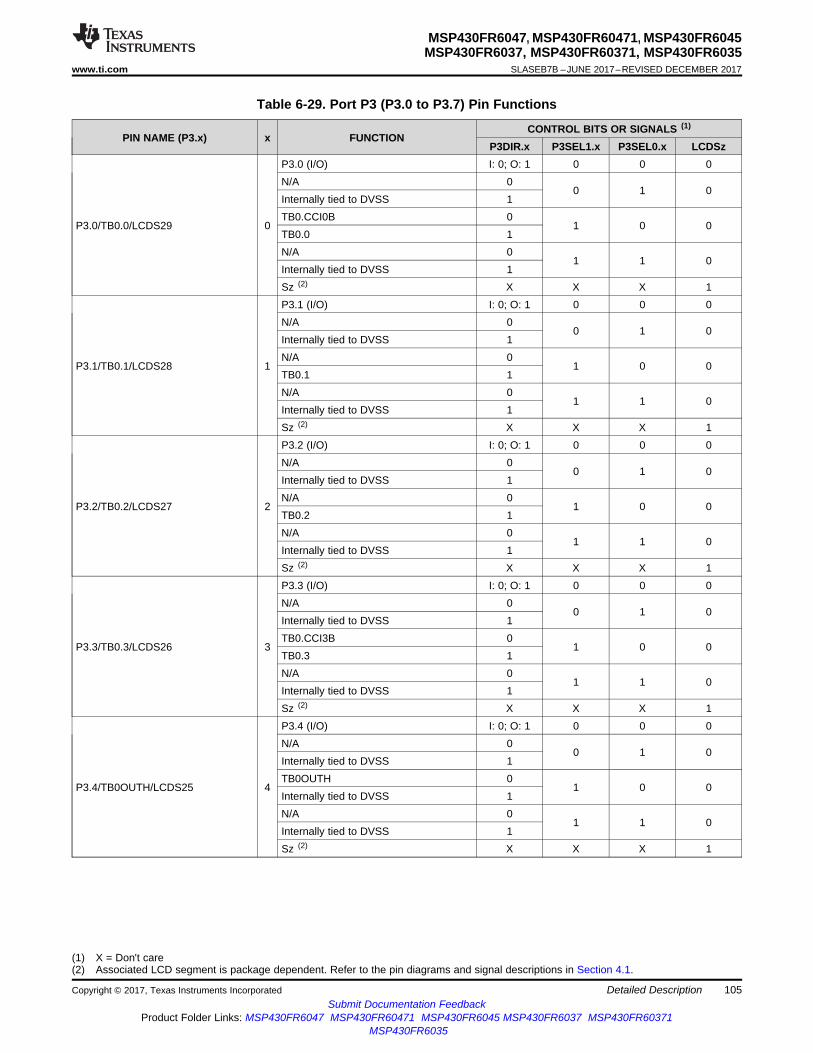
105
MSP430FR6047, MSP430FR60471, MSP430FR6045MSP430FR6037, MSP430FR60371, MSP430FR6035
www.ti.com SLASEB7B –JUNE 2017–REVISED DECEMBER 2017
Submit Documentation FeedbackProduct Folder Links: MSP430FR6047 MSP430FR60471 MSP430FR6045 MSP430FR6037 MSP430FR60371
MSP430FR6035
Detailed DescriptionCopyright © 2017, Texas Instruments Incorporated
(1) X = Don't care(2) Associated LCD segment is package dependent. Refer to the pin diagrams and signal descriptions in Section 4.1.
Table 6-29. Port P3 (P3.0 to P3.7) Pin Functions
PIN NAME (P3.x) x FUNCTIONCONTROL BITS OR SIGNALS (1)
P3DIR.x P3SEL1.x P3SEL0.x LCDSz
P3.0/TB0.0/LCDS29 0
P3.0 (I/O) I: 0; O: 1 0 0 0N/A 0
0 1 0Internally tied to DVSS 1TB0.CCI0B 0
1 0 0TB0.0 1N/A 0
1 1 0Internally tied to DVSS 1Sz (2) X X X 1
P3.1/TB0.1/LCDS28 1
P3.1 (I/O) I: 0; O: 1 0 0 0N/A 0
0 1 0Internally tied to DVSS 1N/A 0
1 0 0TB0.1 1N/A 0
1 1 0Internally tied to DVSS 1Sz (2) X X X 1
P3.2/TB0.2/LCDS27 2
P3.2 (I/O) I: 0; O: 1 0 0 0N/A 0
0 1 0Internally tied to DVSS 1N/A 0
1 0 0TB0.2 1N/A 0
1 1 0Internally tied to DVSS 1Sz (2) X X X 1
P3.3/TB0.3/LCDS26 3
P3.3 (I/O) I: 0; O: 1 0 0 0N/A 0
0 1 0Internally tied to DVSS 1TB0.CCI3B 0
1 0 0TB0.3 1N/A 0
1 1 0Internally tied to DVSS 1Sz (2) X X X 1
P3.4/TB0OUTH/LCDS25 4
P3.4 (I/O) I: 0; O: 1 0 0 0N/A 0
0 1 0Internally tied to DVSS 1TB0OUTH 0
1 0 0Internally tied to DVSS 1N/A 0
1 1 0Internally tied to DVSS 1Sz (2) X X X 1

106
MSP430FR6047, MSP430FR60471, MSP430FR6045MSP430FR6037, MSP430FR60371, MSP430FR6035SLASEB7B –JUNE 2017–REVISED DECEMBER 2017 www.ti.com
Submit Documentation FeedbackProduct Folder Links: MSP430FR6047 MSP430FR60471 MSP430FR6045 MSP430FR6037 MSP430FR60371
MSP430FR6035
Detailed Description Copyright © 2017, Texas Instruments Incorporated
Table 6-29. Port P3 (P3.0 to P3.7) Pin Functions (continued)
PIN NAME (P3.x) x FUNCTIONCONTROL BITS OR SIGNALS (1)
P3DIR.x P3SEL1.x P3SEL0.x LCDSz
P3.5/TB0.4/LCDS24 5
P3.5 (I/O) I: 0; O: 1 0 0 0N/A 0
0 1 0Internally tied to DVSS 1TB0.CCI4B 0
1 0 0TB0.4 1N/A 0
1 1 0Internally tied to DVSS 1Sz (2) X X X 1
P3.6/TB0.5/LCDS23 6
P3.6 (I/O) I: 0; O: 1 0 0 0N/A 0
0 1 0Internally tied to DVSS 1TB0.CCI5B 0
1 0 0TB0.5 1N/A 0
1 1 0Internally tied to DVSS 1Sz (2) X X X 1
P3.7/TB0.6/LCDS22 7
P3.7 (I/O) I: 0; O: 1 0 0 0N/A 0
0 1 0Internally tied to DVSS 1TB0.CCI6B 0
1 0 0TB0.6 1N/A 0
1 1 0Internally tied to DVSS 1Sz (2) X X X 1

PxSEL1.x
PxDIR.x
PxIN.x
EN
To modules
PxOUT.x
1
0DVSS
DVCC 1
D
Pad Logic
Sz
LCDSz
BusKeeper
Direction0: Input1: Output
PxREN.x
0 1
0 0
1 0
1 1
PxSEL0.x
0 1
0 0
1 0
1 1
module 1 or DVSS
module 2 or DVSS
module 3 or DVSS
module 1 or PxDIR.x
module 2 or PxDIR.x
module 3 or PxDIR.x
107
MSP430FR6047, MSP430FR60471, MSP430FR6045MSP430FR6037, MSP430FR60371, MSP430FR6035
www.ti.com SLASEB7B –JUNE 2017–REVISED DECEMBER 2017
Submit Documentation FeedbackProduct Folder Links: MSP430FR6047 MSP430FR60471 MSP430FR6045 MSP430FR6037 MSP430FR60371
MSP430FR6035
Detailed DescriptionCopyright © 2017, Texas Instruments Incorporated
(1) X = Don't care(2) Associated LCD segment is package dependent. Refer to the pin diagrams and signal descriptions in Section 4.1.
6.14.7 Port P4 (P4.0 to P4.7) Input/Output With Schmitt TriggerFigure 6-8 shows the port diagram. Table 6-30 summarizes the selection of the pin function.
NOTE: Functional representation only.
Figure 6-8. Port P4 (P4.0 to P4.7) Diagram
Table 6-30. Port P4 (P4.0 to P4.7) Pin Functions
PIN NAME (P4.x) x FUNCTIONCONTROL BITS OR SIGNALS (1)
P4DIR.x P4SEL1.x P4SEL0.x LCDSz
P4.0/RTCCLK/LCDS16 0
P4.0 (I/O) I: 0; O: 1 0 0 0N/A 0
0 1 0Internally tied to DVSS 1N/A 0
1 0 0RTCCLK 1N/A 0
1 1 0Internally tied to DVSS 1Sz (2) X X X 1
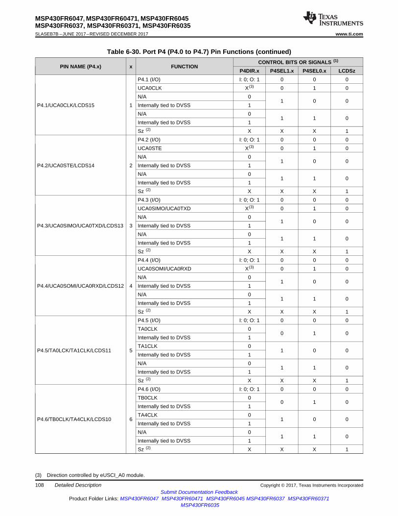
108
MSP430FR6047, MSP430FR60471, MSP430FR6045MSP430FR6037, MSP430FR60371, MSP430FR6035SLASEB7B –JUNE 2017–REVISED DECEMBER 2017 www.ti.com
Submit Documentation FeedbackProduct Folder Links: MSP430FR6047 MSP430FR60471 MSP430FR6045 MSP430FR6037 MSP430FR60371
MSP430FR6035
Detailed Description Copyright © 2017, Texas Instruments Incorporated
Table 6-30. Port P4 (P4.0 to P4.7) Pin Functions (continued)
PIN NAME (P4.x) x FUNCTIONCONTROL BITS OR SIGNALS (1)
P4DIR.x P4SEL1.x P4SEL0.x LCDSz
(3) Direction controlled by eUSCI_A0 module.
P4.1/UCA0CLK/LCDS15 1
P4.1 (I/O) I: 0; O: 1 0 0 0UCA0CLK X (3) 0 1 0N/A 0
1 0 0Internally tied to DVSS 1N/A 0
1 1 0Internally tied to DVSS 1Sz (2) X X X 1
P4.2/UCA0STE/LCDS14 2
P4.2 (I/O) I: 0; O: 1 0 0 0UCA0STE X (3) 0 1 0N/A 0
1 0 0Internally tied to DVSS 1N/A 0
1 1 0Internally tied to DVSS 1Sz (2) X X X 1
P4.3/UCA0SIMO/UCA0TXD/LCDS13 3
P4.3 (I/O) I: 0; O: 1 0 0 0UCA0SIMO/UCA0TXD X (3) 0 1 0N/A 0
1 0 0Internally tied to DVSS 1N/A 0
1 1 0Internally tied to DVSS 1Sz (2) X X X 1
P4.4/UCA0SOMI/UCA0RXD/LCDS12 4
P4.4 (I/O) I: 0; O: 1 0 0 0UCA0SOMI/UCA0RXD X (3) 0 1 0N/A 0
1 0 0Internally tied to DVSS 1N/A 0
1 1 0Internally tied to DVSS 1Sz (2) X X X 1
P4.5/TA0LCK/TA1CLK/LCDS11 5
P4.5 (I/O) I: 0; O: 1 0 0 0TA0CLK 0
0 1 0Internally tied to DVSS 1TA1CLK 0
1 0 0Internally tied to DVSS 1N/A 0
1 1 0Internally tied to DVSS 1Sz (2) X X X 1
P4.6/TB0CLK/TA4CLK/LCDS10 6
P4.6 (I/O) I: 0; O: 1 0 0 0TB0CLK 0
0 1 0Internally tied to DVSS 1TA4CLK 0
1 0 0Internally tied to DVSS 1N/A 0
1 1 0Internally tied to DVSS 1Sz (2) X X X 1
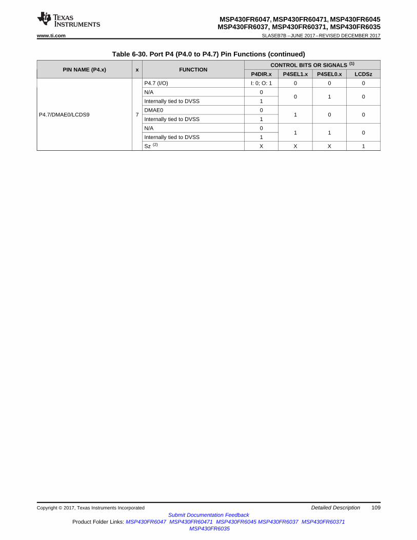
109
MSP430FR6047, MSP430FR60471, MSP430FR6045MSP430FR6037, MSP430FR60371, MSP430FR6035
www.ti.com SLASEB7B –JUNE 2017–REVISED DECEMBER 2017
Submit Documentation FeedbackProduct Folder Links: MSP430FR6047 MSP430FR60471 MSP430FR6045 MSP430FR6037 MSP430FR60371
MSP430FR6035
Detailed DescriptionCopyright © 2017, Texas Instruments Incorporated
Table 6-30. Port P4 (P4.0 to P4.7) Pin Functions (continued)
PIN NAME (P4.x) x FUNCTIONCONTROL BITS OR SIGNALS (1)
P4DIR.x P4SEL1.x P4SEL0.x LCDSz
P4.7/DMAE0/LCDS9 7
P4.7 (I/O) I: 0; O: 1 0 0 0N/A 0
0 1 0Internally tied to DVSS 1DMAE0 0
1 0 0Internally tied to DVSS 1N/A 0
1 1 0Internally tied to DVSS 1Sz (2) X X X 1
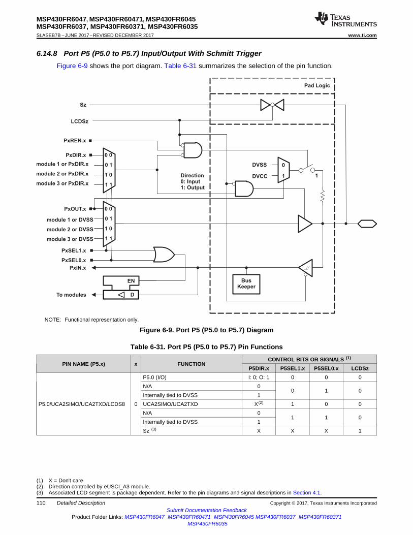
PxSEL1.x
PxDIR.x
PxIN.x
EN
To modules
PxOUT.x
1
0DVSS
DVCC 1
D
Pad Logic
Sz
LCDSz
BusKeeper
Direction0: Input1: Output
PxREN.x
0 1
0 0
1 0
1 1
PxSEL0.x
0 1
0 0
1 0
1 1
module 1 or DVSS
module 2 or DVSS
module 3 or DVSS
module 1 or PxDIR.x
module 2 or PxDIR.x
module 3 or PxDIR.x
110
MSP430FR6047, MSP430FR60471, MSP430FR6045MSP430FR6037, MSP430FR60371, MSP430FR6035SLASEB7B –JUNE 2017–REVISED DECEMBER 2017 www.ti.com
Submit Documentation FeedbackProduct Folder Links: MSP430FR6047 MSP430FR60471 MSP430FR6045 MSP430FR6037 MSP430FR60371
MSP430FR6035
Detailed Description Copyright © 2017, Texas Instruments Incorporated
(1) X = Don't care(2) Direction controlled by eUSCI_A3 module.(3) Associated LCD segment is package dependent. Refer to the pin diagrams and signal descriptions in Section 4.1.
6.14.8 Port P5 (P5.0 to P5.7) Input/Output With Schmitt TriggerFigure 6-9 shows the port diagram. Table 6-31 summarizes the selection of the pin function.
NOTE: Functional representation only.
Figure 6-9. Port P5 (P5.0 to P5.7) Diagram
Table 6-31. Port P5 (P5.0 to P5.7) Pin Functions
PIN NAME (P5.x) x FUNCTIONCONTROL BITS OR SIGNALS (1)
P5DIR.x P5SEL1.x P5SEL0.x LCDSz
P5.0/UCA2SIMO/UCA2TXD/LCDS8 0
P5.0 (I/O) I: 0; O: 1 0 0 0N/A 0
0 1 0Internally tied to DVSS 1UCA2SIMO/UCA2TXD X (2) 1 0 0N/A 0
1 1 0Internally tied to DVSS 1Sz (3) X X X 1
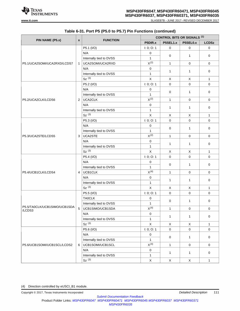
111
MSP430FR6047, MSP430FR60471, MSP430FR6045MSP430FR6037, MSP430FR60371, MSP430FR6035
www.ti.com SLASEB7B –JUNE 2017–REVISED DECEMBER 2017
Submit Documentation FeedbackProduct Folder Links: MSP430FR6047 MSP430FR60471 MSP430FR6045 MSP430FR6037 MSP430FR60371
MSP430FR6035
Detailed DescriptionCopyright © 2017, Texas Instruments Incorporated
Table 6-31. Port P5 (P5.0 to P5.7) Pin Functions (continued)
PIN NAME (P5.x) x FUNCTIONCONTROL BITS OR SIGNALS (1)
P5DIR.x P5SEL1.x P5SEL0.x LCDSz
(4) Direction controlled by eUSCI_B1 module.
P5.1/UCA2SOMI/UCA2RXD/LCDS7 1
P5.1 (I/O) I: 0; O: 1 0 0 0N/A 0
0 1 0Internally tied to DVSS 1UCA2SOMI/UCA2RXD X (2) 1 0 0N/A 0
1 1 0Internally tied to DVSS 1Sz (3) X X X 1
P5.2/UCA2CLK/LCDS6 2
P5.2 (I/O) I: 0; O: 1 0 0 0N/A 0
0 1 0Internally tied to DVSS 1UCA2CLK X (2) 1 0 0N/A 0
1 1 0Internally tied to DVSS 1Sz (3) X X X 1
P5.3/UCA2STE/LCDS5 3
P5.3 (I/O) I: 0; O: 1 0 0 0N/A 0
0 1 0Internally tied to DVSS 1UCA2STE X (2) 1 0 0N/A 0
1 1 0Internally tied to DVSS 1Sz (3) X X X 1
P5.4/UCB1CLK/LCDS4 4
P5.4 (I/O) I: 0; O: 1 0 0 0N/A 0
0 1 0Internally tied to DVSS 1UCB1CLK X (4) 1 0 0N/A 0
1 1 0Internally tied to DVSS 1Sz (3) X X X 1
P5.5/TA0CLK/UCB1SIMO/UCB1SDA/LCDS3 5
P5.5 (I/O) I: 0; O: 1 0 0 0TA0CLK 0
0 1 0Internally tied to DVSS 1UCB1SIMO/UCB1SDA X (4) 1 0 0N/A 0
1 1 0Internally tied to DVSS 1Sz (3) X X X 1
P5.6/UCB1SOMI/UCB1SCL/LCDS2 6
P5.6 (I/O) I: 0; O: 1 0 0 0N/A 0
0 1 0Internally tied to DVSS 1UCB1SOMI/UCB1SCL X (4) 1 0 0N/A 0
1 1 0Internally tied to DVSS 1Sz (3) X X X 1

112
MSP430FR6047, MSP430FR60471, MSP430FR6045MSP430FR6037, MSP430FR60371, MSP430FR6035SLASEB7B –JUNE 2017–REVISED DECEMBER 2017 www.ti.com
Submit Documentation FeedbackProduct Folder Links: MSP430FR6047 MSP430FR60471 MSP430FR6045 MSP430FR6037 MSP430FR60371
MSP430FR6035
Detailed Description Copyright © 2017, Texas Instruments Incorporated
Table 6-31. Port P5 (P5.0 to P5.7) Pin Functions (continued)
PIN NAME (P5.x) x FUNCTIONCONTROL BITS OR SIGNALS (1)
P5DIR.x P5SEL1.x P5SEL0.x LCDSz
P5.7/UCB1STE/LCDS1 7
P5.7 (I/O) I: 0; O: 1 0 0 0N/A 0
0 1 0Internally tied to DVSS 1UCB1STE X (4) 1 0 0N/A 0
1 1 0Internally tied to DVSS 1Sz (3) X X X 1

PxSEL1.x
PxDIR.x
PxIN.x
EN
To modules
PxOUT.x
1
0DVSS
DVCC 1
D
Pad Logic
Sz
LCDSz
BusKeeper
Direction0: Input1: Output
PxREN.x
0 1
0 0
1 0
1 1
PxSEL0.x
0 1
0 0
1 0
1 1
module 1 or DVSS
module 2 or DVSS
module 3 or DVSS
module 1 or PxDIR.x
module 2 or PxDIR.x
module 3 or PxDIR.x
113
MSP430FR6047, MSP430FR60471, MSP430FR6045MSP430FR6037, MSP430FR60371, MSP430FR6035
www.ti.com SLASEB7B –JUNE 2017–REVISED DECEMBER 2017
Submit Documentation FeedbackProduct Folder Links: MSP430FR6047 MSP430FR60471 MSP430FR6045 MSP430FR6037 MSP430FR60371
MSP430FR6035
Detailed DescriptionCopyright © 2017, Texas Instruments Incorporated
(1) X = Don't care(2) Associated LCD segment is package dependent. Refer to the pin diagrams and signal descriptions in Section 4.1.
6.14.9 Port P6 (P6.0) Input/Output With Schmitt TriggerFigure 6-10 shows the port diagram. Table 6-32 summarizes the selection of the pin function.
NOTE: Functional representation only.
Figure 6-10. Port P6 (P6.0) Diagram
Table 6-32. Port P6 (P6.0) Pin Functions
PIN NAME (P6.x) x FUNCTIONCONTROL BITS OR SIGNALS (1)
P6DIR.x P6SEL1.x P6SEL0.x LCDSz
P6.0/COUT/LCDS0 0
P6.0 (I/O) I: 0; O: 1 0 0 0N/A 0
0 1 0Internally tied to DVSS 1N/A 0
1 0 0COUT 1N/A 0
1 1 0Internally tied to DVSS 1Sz (2) X X X 1

PxSEL1.x
PxDIR.x
PxIN.x
EN
To modules
PxOUT.x
1
0DVSS
DVCC 1
D
To/From LCD
Pad Logic
BusKeeper
Direction0: Input1: Output
PxREN.x
0 1
0 0
1 0
1 1
PxSEL0.x
0 1
0 0
1 0
1 1
module 1 or DVSS
module 2 or DVSS
module 3 or DVSS
module 1 or PxDIR.x
module 2 or PxDIR.x
module 3 or PxDIR.x
114
MSP430FR6047, MSP430FR60471, MSP430FR6045MSP430FR6037, MSP430FR60371, MSP430FR6035SLASEB7B –JUNE 2017–REVISED DECEMBER 2017 www.ti.com
Submit Documentation FeedbackProduct Folder Links: MSP430FR6047 MSP430FR60471 MSP430FR6045 MSP430FR6037 MSP430FR60371
MSP430FR6035
Detailed Description Copyright © 2017, Texas Instruments Incorporated
6.14.10 Port P6 (P6.1 to P6.5) Input/Output With Schmitt TriggerFigure 6-11 shows the port diagram. Table 6-33 summarizes the selection of the pin function.
NOTE: Functional representation only.
Figure 6-11. Port P6 (P6.1 to P6.5) Diagram

115
MSP430FR6047, MSP430FR60471, MSP430FR6045MSP430FR6037, MSP430FR60371, MSP430FR6035
www.ti.com SLASEB7B –JUNE 2017–REVISED DECEMBER 2017
Submit Documentation FeedbackProduct Folder Links: MSP430FR6047 MSP430FR60471 MSP430FR6045 MSP430FR6037 MSP430FR60371
MSP430FR6035
Detailed DescriptionCopyright © 2017, Texas Instruments Incorporated
(1) X = Don't care(2) Setting P6SEL1.x and P6SEL0.x disables the output driver and the input Schmitt trigger to prevent parasitic cross currents when
applying analog signals.
Table 6-33. Port P6 (P6.1 to P6.5) Pin Functions
PIN NAME (P6.x) x FUNCTIONCONTROL BITS OR SIGNALS (1)
P6DIR.x P6SEL1.x P6SEL0.x
P6.1/R03 1
P6.1 (I/O) I: 0; O: 1 0 0N/A 0
0 1Internally tied to DVSS 1N/A 0
1 0Internally tied to DVSS 1R03 (2) X 1 1
P6.2/R13/LCDREF 2
P6.2 (I/O) I: 0; O: 1 0 0N/A 0
0 1Internally tied to DVSS 1N/A 0
1 0Internally tied to DVSS 1R13/LCDREF (2) X 1 1
P6.3/R23 3
P6.3 (I/O) I: 0; O: 1 0 0N/A 0
0 1Internally tied to DVSS 1N/A 0
1 0Internally tied to DVSS 1R23 (2) X 1 1
P6.4/COM0 4
P6.4 (I/O) I: 0; O: 1 0 0N/A 0
0 1Internally tied to DVSS 1N/A 0
1 0Internally tied to DVSS 1COM0 (2) X 1 1
P6.5/COM1 5
P6.5 (I/O) I: 0; O: 1 0 0N/A 0
0 1Internally tied to DVSS 1N/A 0
1 0Internally tied to DVSS 1COM1 (2) X 1 1

PxSEL1.x
PxDIR.x
PxIN.x
EN
To modules
PxOUT.x
1
0DVSS
DVCC 1
D
COMx
Pad Logic
Sz
LCDSz
BusKeeper
Direction0: Input1: Output
PxREN.x
0 1
0 0
1 0
1 1
PxSEL0.x
0 1
0 0
1 0
1 1
module 1 or DVSS
module 2 or DVSS
module 3 or DVSS
module 1 or PxDIR.x
module 2 or PxDIR.x
module 3 or PxDIR.x
116
MSP430FR6047, MSP430FR60471, MSP430FR6045MSP430FR6037, MSP430FR60371, MSP430FR6035SLASEB7B –JUNE 2017–REVISED DECEMBER 2017 www.ti.com
Submit Documentation FeedbackProduct Folder Links: MSP430FR6047 MSP430FR60471 MSP430FR6045 MSP430FR6037 MSP430FR60371
MSP430FR6035
Detailed Description Copyright © 2017, Texas Instruments Incorporated
6.14.11 Port P6 (P6.6 and P6.7) Input/Output With Schmitt TriggerFigure 6-12 shows the port diagram. Table 6-34 summarizes the selection of the pin function.
NOTE: Functional representation only.
Figure 6-12. Port P6 (P6.6 and P6.7) Diagram

117
MSP430FR6047, MSP430FR60471, MSP430FR6045MSP430FR6037, MSP430FR60371, MSP430FR6035
www.ti.com SLASEB7B –JUNE 2017–REVISED DECEMBER 2017
Submit Documentation FeedbackProduct Folder Links: MSP430FR6047 MSP430FR60471 MSP430FR6045 MSP430FR6037 MSP430FR60371
MSP430FR6035
Detailed DescriptionCopyright © 2017, Texas Instruments Incorporated
(1) Setting P6SEL1.x and P6SEL0.x disables the output driver and the input Schmitt trigger to prevent parasitic cross currents whenapplying analog signals.
(2) Associated LCD segment is package dependent. Refer to the pin diagrams and signal descriptions in Section 4.1.
Table 6-34. Port P6 (P6.6 to P6.7) Pin Functions
PIN NAME (P6.x) x FUNCTIONCONTROL BITS OR SIGNALS
P6DIR.x P6SEL1.x P6SEL0.x LCDSz
P6.6/COM2/LCDS38 6
P6.6(I/O) I: 0; O: 1 0 0 0N/A 0
0 1 0Internally tied to DVSS 1N/A 0
1 0 0Internally tied to DVSS 1COM2 (1) X 1 1 0
Sz (2) XX 0
10 X
P6.7/COM3/LCDS37 7
P6.7(I/O) I: 0; O: 1 0 0 0N/A 0
0 1 0Internally tied to DVSS 1N/A 0
1 0 0Internally tied to DVSS 1COM3 (1) X 1 1 0
Sz (2) XX 0
10 X
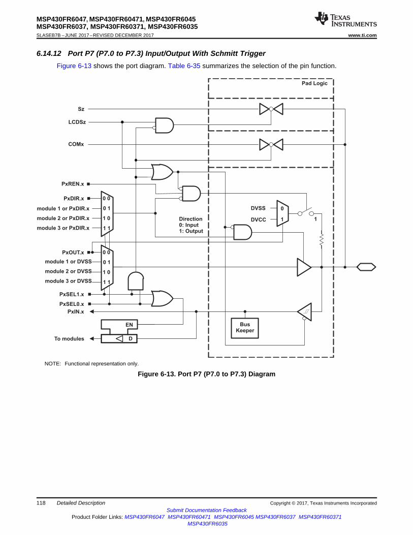
PxSEL1.x
PxDIR.x
PxIN.x
EN
To modules
PxOUT.x
1
0DVSS
DVCC 1
D
COMx
Pad Logic
Sz
LCDSz
BusKeeper
Direction0: Input1: Output
PxREN.x
0 1
0 0
1 0
1 1
PxSEL0.x
0 1
0 0
1 0
1 1
module 1 or DVSS
module 2 or DVSS
module 3 or DVSS
module 1 or PxDIR.x
module 2 or PxDIR.x
module 3 or PxDIR.x
118
MSP430FR6047, MSP430FR60471, MSP430FR6045MSP430FR6037, MSP430FR60371, MSP430FR6035SLASEB7B –JUNE 2017–REVISED DECEMBER 2017 www.ti.com
Submit Documentation FeedbackProduct Folder Links: MSP430FR6047 MSP430FR60471 MSP430FR6045 MSP430FR6037 MSP430FR60371
MSP430FR6035
Detailed Description Copyright © 2017, Texas Instruments Incorporated
6.14.12 Port P7 (P7.0 to P7.3) Input/Output With Schmitt TriggerFigure 6-13 shows the port diagram. Table 6-35 summarizes the selection of the pin function.
NOTE: Functional representation only.
Figure 6-13. Port P7 (P7.0 to P7.3) Diagram
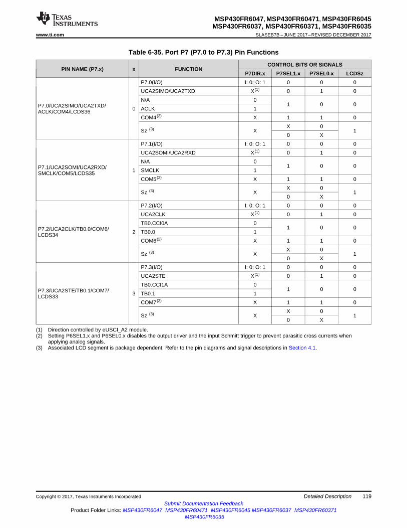
119
MSP430FR6047, MSP430FR60471, MSP430FR6045MSP430FR6037, MSP430FR60371, MSP430FR6035
www.ti.com SLASEB7B –JUNE 2017–REVISED DECEMBER 2017
Submit Documentation FeedbackProduct Folder Links: MSP430FR6047 MSP430FR60471 MSP430FR6045 MSP430FR6037 MSP430FR60371
MSP430FR6035
Detailed DescriptionCopyright © 2017, Texas Instruments Incorporated
(1) Direction controlled by eUSCI_A2 module.(2) Setting P6SEL1.x and P6SEL0.x disables the output driver and the input Schmitt trigger to prevent parasitic cross currents when
applying analog signals.(3) Associated LCD segment is package dependent. Refer to the pin diagrams and signal descriptions in Section 4.1.
Table 6-35. Port P7 (P7.0 to P7.3) Pin Functions
PIN NAME (P7.x) x FUNCTIONCONTROL BITS OR SIGNALS
P7DIR.x P7SEL1.x P7SEL0.x LCDSz
P7.0/UCA2SIMO/UCA2TXD/ACLK/COM4/LCDS36 0
P7.0(I/O) I: 0; O: 1 0 0 0UCA2SIMO/UCA2TXD X (1) 0 1 0N/A 0
1 0 0ACLK 1COM4 (2) X 1 1 0
Sz (3) XX 0
10 X
P7.1/UCA2SOMI/UCA2RXD/SMCLK/COM5/LCDS35 1
P7.1(I/O) I: 0; O: 1 0 0 0UCA2SOMI/UCA2RXD X (1) 0 1 0N/A 0
1 0 0SMCLK 1COM5 (2) X 1 1 0
Sz (3) XX 0
10 X
P7.2/UCA2CLK/TB0.0/COM6/LCDS34 2
P7.2(I/O) I: 0; O: 1 0 0 0UCA2CLK X (1) 0 1 0TB0.CCI0A 0
1 0 0TB0.0 1COM6 (2) X 1 1 0
Sz (3) XX 0
10 X
P7.3/UCA2STE/TB0.1/COM7/LCDS33 3
P7.3(I/O) I: 0; O: 1 0 0 0UCA2STE X (1) 0 1 0TB0.CCI1A 0
1 0 0TB0.1 1COM7 (2) X 1 1 0
Sz (3) XX 0
10 X
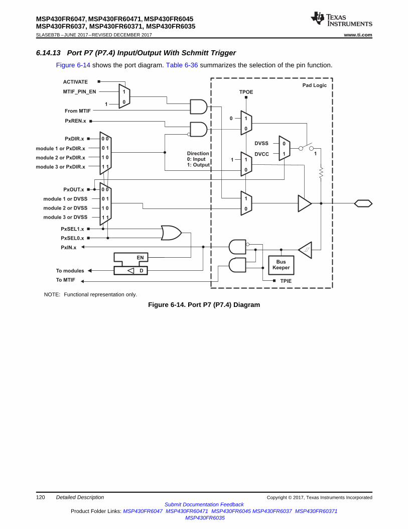
PxSEL1.x
PxDIR.x
PxIN.x
EN
To modules
PxOUT.x
1
0DVSS
DVCC 1
D
Pad Logic
BusKeeper
Direction0: Input1: Output
PxREN.x
0 1
0 0
1 0
1 1
PxSEL0.x
0 1
0 0
1 0
1 1
MTIF_PIN_EN
From MTIF
module 1 or DVSS
module 2 or DVSS
module 3 or DVSS
module 1 or PxDIR.x
module 2 or PxDIR.x
module 3 or PxDIR.x
0
1
0
1
0
1
0
1
TPOE
TPIETo MTIF
0
1
ACTIVATE
1
120
MSP430FR6047, MSP430FR60471, MSP430FR6045MSP430FR6037, MSP430FR60371, MSP430FR6035SLASEB7B –JUNE 2017–REVISED DECEMBER 2017 www.ti.com
Submit Documentation FeedbackProduct Folder Links: MSP430FR6047 MSP430FR60471 MSP430FR6045 MSP430FR6037 MSP430FR60371
MSP430FR6035
Detailed Description Copyright © 2017, Texas Instruments Incorporated
6.14.13 Port P7 (P7.4) Input/Output With Schmitt TriggerFigure 6-14 shows the port diagram. Table 6-36 summarizes the selection of the pin function.
NOTE: Functional representation only.
Figure 6-14. Port P7 (P7.4) Diagram

121
MSP430FR6047, MSP430FR60471, MSP430FR6045MSP430FR6037, MSP430FR60371, MSP430FR6035
www.ti.com SLASEB7B –JUNE 2017–REVISED DECEMBER 2017
Submit Documentation FeedbackProduct Folder Links: MSP430FR6047 MSP430FR60471 MSP430FR6045 MSP430FR6037 MSP430FR60371
MSP430FR6035
Detailed DescriptionCopyright © 2017, Texas Instruments Incorporated
(1) See MTIF.TPCTL register(2) When P7.5 pin is configured as MTIF_PIN_EN (See Table 6-37 for details)
Table 6-36. Port P7 (P7.4) Pin Functions
PIN NAME (P7.x) x FUNCTION
CONTROL BITS OR SIGNALS
P7DIR.x P7SEL1.x P7SEL0.x TPOE (1) TPIE (1) ACTIVATE
(1)Signal on
MTIF_PIN_EN pin (2)
P7.4/TA0.1/MTIF_OUT_IN 4
P7.4(I/O) I: 0; O: 1 0 0 0 0 X XTA0.CCI1A 0
0 1 0 0 X XTA0.1 1N/A 0
1 0 0 0 X XInternally tied to DVSS 1N/A 0
1 1 0 0 X XInternally tied to DVSS 1MTIF_IN X X X 0 1 X XMTIF_OUT (1) X X X 1 X 0 XInternally tied toDVSS (1) X X X 1 X 1 0
MTIF_OUT (1) X X X 1 X 1 1
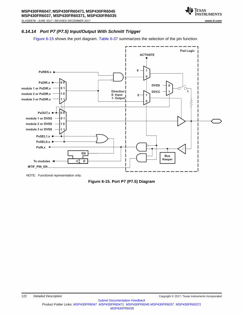
PxSEL1.x
PxDIR.x
PxIN.x
EN
To modules
PxOUT.x
1
0DVSS
DVCC 1
D
Pad Logic
BusKeeper
Direction0: Input1: Output
PxREN.x
0 1
0 0
1 0
1 1
PxSEL0.x
0 1
0 0
1 0
1 1
module 1 or DVSS
module 2 or DVSS
module 3 or DVSS
module 1 or PxDIR.x
module 2 or PxDIR.x
module 3 or PxDIR.x
0
1
0
1
0
0
ACTIVATE
MTIF_PIN_EN
122
MSP430FR6047, MSP430FR60471, MSP430FR6045MSP430FR6037, MSP430FR60371, MSP430FR6035SLASEB7B –JUNE 2017–REVISED DECEMBER 2017 www.ti.com
Submit Documentation FeedbackProduct Folder Links: MSP430FR6047 MSP430FR60471 MSP430FR6045 MSP430FR6037 MSP430FR60371
MSP430FR6035
Detailed Description Copyright © 2017, Texas Instruments Incorporated
6.14.14 Port P7 (P7.5) Input/Output With Schmitt TriggerFigure 6-15 shows the port diagram. Table 6-37 summarizes the selection of the pin function.
NOTE: Functional representation only.
Figure 6-15. Port P7 (P7.5) Diagram

123
MSP430FR6047, MSP430FR60471, MSP430FR6045MSP430FR6037, MSP430FR60371, MSP430FR6035
www.ti.com SLASEB7B –JUNE 2017–REVISED DECEMBER 2017
Submit Documentation FeedbackProduct Folder Links: MSP430FR6047 MSP430FR60471 MSP430FR6045 MSP430FR6037 MSP430FR60371
MSP430FR6035
Detailed DescriptionCopyright © 2017, Texas Instruments Incorporated
(1) See MTIF.TPCTL register
Table 6-37. Port P7 (P7.5) Pin Functions
PIN NAME (P7.x) x FUNCTIONCONTROL BITS OR SIGNALS
P7DIR.x P7SEL1.x P7SEL0.x ACTIVATE (1)
P7.5/TA1.1/MTIF_PIN_EN 5
P7.5(I/O) I: 0; O: 1 0 0 0TA1.CCI1A 0
0 1 0TA1.1 1N/A 0
1 0 0Internally tied to DVSS 1N/A 0
1 1 0Internally tied to DVSS 1MTIF_PIN_EN X X X 1

PxSEL1.x
PxDIR.x
PxIN.x
EN
To modules
PxOUT.x
1
0DVSS
DVCC 1
D
Pad Logic
Direction0: Input1: Output
PxREN.x
0 1
0 0
1 0
1 1
PxSEL0.x
0 1
0 0
1 0
1 1
module 1 or DVSS
module 2 or DVSS
module 3 or DVSS
module 1 or PxDIR.x
module 2 or PxDIR.x
module 3 or PxDIR.x
124
MSP430FR6047, MSP430FR60471, MSP430FR6045MSP430FR6037, MSP430FR60371, MSP430FR6035SLASEB7B –JUNE 2017–REVISED DECEMBER 2017 www.ti.com
Submit Documentation FeedbackProduct Folder Links: MSP430FR6047 MSP430FR60471 MSP430FR6045 MSP430FR6037 MSP430FR60371
MSP430FR6035
Detailed Description Copyright © 2017, Texas Instruments Incorporated
6.14.15 Port P7 (P7.6 and P7.7) Input/Output With Schmitt TriggerFigure 6-16 shows the port diagram. Table 6-38 summarizes the selection of the pin function.
NOTE: Functional representation only.
Figure 6-16. Port P7 (P7.6 and P7.7) Diagram
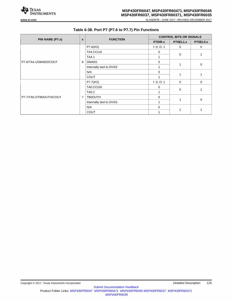
125
MSP430FR6047, MSP430FR60471, MSP430FR6045MSP430FR6037, MSP430FR60371, MSP430FR6035
www.ti.com SLASEB7B –JUNE 2017–REVISED DECEMBER 2017
Submit Documentation FeedbackProduct Folder Links: MSP430FR6047 MSP430FR60471 MSP430FR6045 MSP430FR6037 MSP430FR60371
MSP430FR6035
Detailed DescriptionCopyright © 2017, Texas Instruments Incorporated
Table 6-38. Port P7 (P7.6 to P7.7) Pin Functions
PIN NAME (P7.x) x FUNCTIONCONTROL BITS OR SIGNALS
P7DIR.x P7SEL1.x P7SEL0.x
P7.6/TA4.1/DMAE0/COUT 6
P7.6(I/O) I: 0; O: 1 0 0TA4.CCI1A 0
0 1TA4.1 1DMAE0 0
1 0Internally tied to DVSS 1N/A 0
1 1COUT 1
P7.7/TA0.2/TB0OUTH/COUT 7
P7.7(I/O) I: 0; O: 1 0 0TA0.CCI2A 0
0 1TA0.2 1TB0OUTH 0
1 0Internally tied to DVSS 1N/A 0
1 1COUT 1

PxSEL1.x
PxDIR.x
PxIN.x
EN
To modules
PxOUT.x
1
0DVSS
DVCC 1
D
Pad Logic
Direction0: Input1: Output
PxREN.x
0 1
0 0
1 0
1 1
PxSEL0.x
0 1
0 0
1 0
1 1
module 1 or DVSS
module 2 or DVSS
module 3 or DVSS
module 1 or PxDIR.x
module 2 or PxDIR.x
module 3 or PxDIR.x
126
MSP430FR6047, MSP430FR60471, MSP430FR6045MSP430FR6037, MSP430FR60371, MSP430FR6035SLASEB7B –JUNE 2017–REVISED DECEMBER 2017 www.ti.com
Submit Documentation FeedbackProduct Folder Links: MSP430FR6047 MSP430FR60471 MSP430FR6045 MSP430FR6037 MSP430FR60371
MSP430FR6035
Detailed Description Copyright © 2017, Texas Instruments Incorporated
6.14.16 Port P8 (P8.0 to P8.3) Input/Output With Schmitt TriggerFigure 6-17 shows the port diagram. Table 6-39 summarizes the selection of the pin function.
NOTE: Functional representation only.
Figure 6-17. Port P8 (P8.0 to P8.3) Diagram
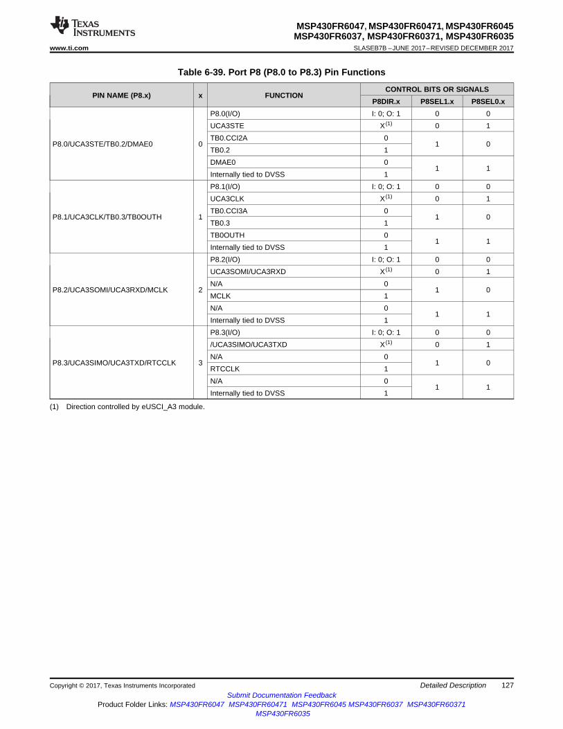
127
MSP430FR6047, MSP430FR60471, MSP430FR6045MSP430FR6037, MSP430FR60371, MSP430FR6035
www.ti.com SLASEB7B –JUNE 2017–REVISED DECEMBER 2017
Submit Documentation FeedbackProduct Folder Links: MSP430FR6047 MSP430FR60471 MSP430FR6045 MSP430FR6037 MSP430FR60371
MSP430FR6035
Detailed DescriptionCopyright © 2017, Texas Instruments Incorporated
(1) Direction controlled by eUSCI_A3 module.
Table 6-39. Port P8 (P8.0 to P8.3) Pin Functions
PIN NAME (P8.x) x FUNCTIONCONTROL BITS OR SIGNALS
P8DIR.x P8SEL1.x P8SEL0.x
P8.0/UCA3STE/TB0.2/DMAE0 0
P8.0(I/O) I: 0; O: 1 0 0UCA3STE X (1) 0 1TB0.CCI2A 0
1 0TB0.2 1DMAE0 0
1 1Internally tied to DVSS 1
P8.1/UCA3CLK/TB0.3/TB0OUTH 1
P8.1(I/O) I: 0; O: 1 0 0UCA3CLK X (1) 0 1TB0.CCI3A 0
1 0TB0.3 1TB0OUTH 0
1 1Internally tied to DVSS 1
P8.2/UCA3SOMI/UCA3RXD/MCLK 2
P8.2(I/O) I: 0; O: 1 0 0UCA3SOMI/UCA3RXD X (1) 0 1N/A 0
1 0MCLK 1N/A 0
1 1Internally tied to DVSS 1
P8.3/UCA3SIMO/UCA3TXD/RTCCLK 3
P8.3(I/O) I: 0; O: 1 0 0/UCA3SIMO/UCA3TXD X (1) 0 1N/A 0
1 0RTCCLK 1N/A 0
1 1Internally tied to DVSS 1
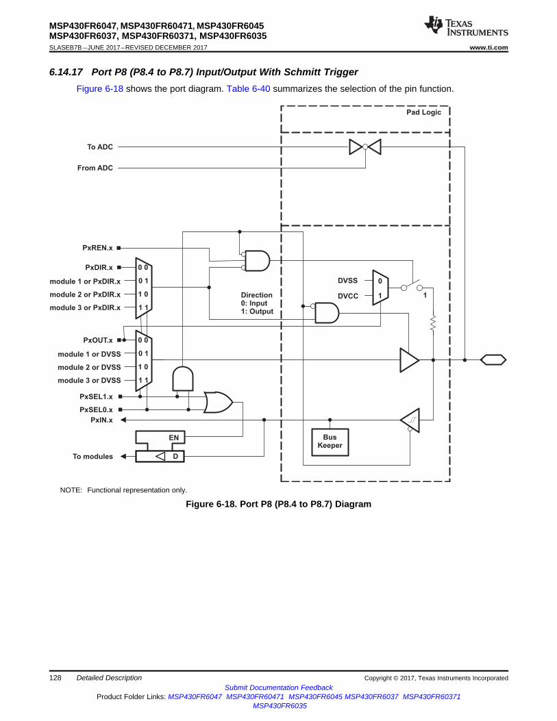
PxSEL1.x
PxDIR.x
PxIN.x
EN
To modules
PxOUT.x
1
0DVSS
DVCC 1
D
Pad Logic
To ADC
From ADC
BusKeeper
Direction0: Input1: Output
PxREN.x
0 1
0 0
1 0
1 1
PxSEL0.x
0 1
0 0
1 0
1 1
module 1 or DVSS
module 2 or DVSS
module 3 or DVSS
module 1 or PxDIR.x
module 2 or PxDIR.x
module 3 or PxDIR.x
128
MSP430FR6047, MSP430FR60471, MSP430FR6045MSP430FR6037, MSP430FR60371, MSP430FR6035SLASEB7B –JUNE 2017–REVISED DECEMBER 2017 www.ti.com
Submit Documentation FeedbackProduct Folder Links: MSP430FR6047 MSP430FR60471 MSP430FR6045 MSP430FR6037 MSP430FR60371
MSP430FR6035
Detailed Description Copyright © 2017, Texas Instruments Incorporated
6.14.17 Port P8 (P8.4 to P8.7) Input/Output With Schmitt TriggerFigure 6-18 shows the port diagram. Table 6-40 summarizes the selection of the pin function.
NOTE: Functional representation only.
Figure 6-18. Port P8 (P8.4 to P8.7) Diagram
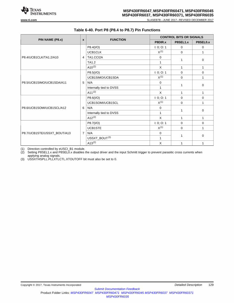
129
MSP430FR6047, MSP430FR60471, MSP430FR6045MSP430FR6037, MSP430FR60371, MSP430FR6035
www.ti.com SLASEB7B –JUNE 2017–REVISED DECEMBER 2017
Submit Documentation FeedbackProduct Folder Links: MSP430FR6047 MSP430FR60471 MSP430FR6045 MSP430FR6037 MSP430FR60371
MSP430FR6035
Detailed DescriptionCopyright © 2017, Texas Instruments Incorporated
(1) Direction controlled by eUSCI_B1 module.(2) Setting P8SEL1.x and P8SEL0.x disables the output driver and the input Schmitt trigger to prevent parasitic cross currents when
applying analog signals.(3) USSXTHSPLL.PLLXTLCTL.XTOUTOFF bit must also be set to 0.
Table 6-40. Port P8 (P8.4 to P8.7) Pin Functions
PIN NAME (P8.x) x FUNCTIONCONTROL BITS OR SIGNALS
P8DIR.x P8SEL1.x P8SEL0.x
P8.4/UCB1CLK/TA1.2/A10 4
P8.4(I/O) I: 0; O: 1 0 0UCB1CLK X (1) 0 1TA1.CCI2A 0
1 0TA1.2 1A10 (2) X 1 1
P8.5/UCB1SIMO/UCB1SDA/A11 5
P8.5(I/O) I: 0; O: 1 0 0UCB1SIMO/UCB1SDA X (1) 0 1N/A 0
1 0Internally tied to DVSS 1A11 (2) X 1 1
P8.6/UCB1SOMI/UCB1SCL/A12 6
P8.6(I/O) I: 0; O: 1 0 0UCB1SOMI/UCB1SCL X (1) 0 1N/A 0
1 0Internally tied to DVSS 1A12 (2) X 1 1
P8.7/UCB1STE/USSXT_BOUT/A13 7
P8.7(I/O) I: 0; O: 1 0 0UCB1STE X (1) 0 1N/A 0
1 0USSXT_BOUT (3) 1A13 (2) X 1 1
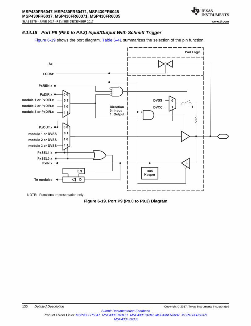
PxSEL1.x
PxDIR.x
PxIN.x
EN
To modules
PxOUT.x
1
0DVSS
DVCC 1
D
Pad Logic
Sz
LCDSz
BusKeeper
Direction0: Input1: Output
PxREN.x
0 1
0 0
1 0
1 1
PxSEL0.x
0 1
0 0
1 0
1 1
module 1 or DVSS
module 2 or DVSS
module 3 or DVSS
module 1 or PxDIR.x
module 2 or PxDIR.x
module 3 or PxDIR.x
130
MSP430FR6047, MSP430FR60471, MSP430FR6045MSP430FR6037, MSP430FR60371, MSP430FR6035SLASEB7B –JUNE 2017–REVISED DECEMBER 2017 www.ti.com
Submit Documentation FeedbackProduct Folder Links: MSP430FR6047 MSP430FR60471 MSP430FR6045 MSP430FR6037 MSP430FR60371
MSP430FR6035
Detailed Description Copyright © 2017, Texas Instruments Incorporated
6.14.18 Port P9 (P9.0 to P9.3) Input/Output With Schmitt TriggerFigure 6-19 shows the port diagram. Table 6-41 summarizes the selection of the pin function.
NOTE: Functional representation only.
Figure 6-19. Port P9 (P9.0 to P9.3) Diagram

131
MSP430FR6047, MSP430FR60471, MSP430FR6045MSP430FR6037, MSP430FR60371, MSP430FR6035
www.ti.com SLASEB7B –JUNE 2017–REVISED DECEMBER 2017
Submit Documentation FeedbackProduct Folder Links: MSP430FR6047 MSP430FR60471 MSP430FR6045 MSP430FR6037 MSP430FR60371
MSP430FR6035
Detailed DescriptionCopyright © 2017, Texas Instruments Incorporated
(1) X = Don't care(2) Associated LCD segment is package dependent. Refer to the pin diagrams and signal descriptions in Section 4.1.
Table 6-41. Port P9 (P9.0 to P9.3) Pin Functions
PIN NAME (P9.x) x FUNCTIONCONTROL BITS OR SIGNALS (1)
P9DIR.x P9SEL1.x P9SEL0.x LCDSz
P9.0/TA1.0/LCDS20 0
P9.0 (I/O) I: 0; O: 1 0 0 0TA1.CCI0B 0
0 1 0TA1.0 1N/A 0
1 0 0Internally tied to DVSS 1N/A 0
1 1 0Internally tied to DVSS 1Sz (2) X X X 1
P9.1/SMCLK/LCDS19 1
P9.1 (I/O) I: 0; O: 1 0 0 0N/A 0
0 1 0Internally tied to DVSS 1N/A 0
1 0 0SMCLK 1N/A 0
1 1 0Internally tied to DVSS 1Sz (2) X X X 1
P9.2/MCLK/LCDS18 2
P9.2 (I/O) I: 0; O: 1 0 0 0N/A 0
0 1 0Internally tied to DVSS 1N/A 0
1 0 0MCLK 1N/A 0
1 1 0Internally tied to DVSS 1Sz (2) X X X 1
P9.3/ACLK/LCDS17 3
P9.3 (I/O) I: 0; O: 1 0 0 0N/A 0
0 1 0Internally tied to DVSS 1N/A 0
1 0 0ACLK 1N/A 0
1 1 0Internally tied to DVSS 1Sz (2) X X X 1
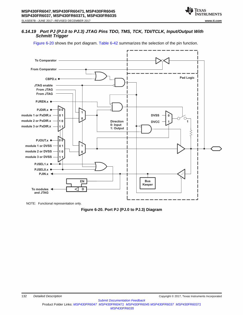
PJSEL1.x
PJDIR.x
PJIN.x
EN
To modulesand JTAG
PJOUT.x
1
0DVSS
DVCC 1
D
Pad Logic
BusKeeper
Direction0: Input1: Output
PJREN.x
0 1
0 0
1 0
1 1
PJSEL0.x
0 1
0 0
1 0
1 1
0
1
0
1
JTAG enable
From JTAG
From JTAG
To Comparator
From Comparator
CBPD.x
module 1 or DVSS
module 2 or DVSS
module 3 or DVSS
module 1 or PxDIR.x
module 2 or PxDIR.x
module 3 or PxDIR.x
132
MSP430FR6047, MSP430FR60471, MSP430FR6045MSP430FR6037, MSP430FR60371, MSP430FR6035SLASEB7B –JUNE 2017–REVISED DECEMBER 2017 www.ti.com
Submit Documentation FeedbackProduct Folder Links: MSP430FR6047 MSP430FR60471 MSP430FR6045 MSP430FR6037 MSP430FR60371
MSP430FR6035
Detailed Description Copyright © 2017, Texas Instruments Incorporated
6.14.19 Port PJ (PJ.0 to PJ.3) JTAG Pins TDO, TMS, TCK, TDI/TCLK, Input/Output WithSchmitt Trigger
Figure 6-20 shows the port diagram. Table 6-42 summarizes the selection of the pin function.
NOTE: Functional representation only.
Figure 6-20. Port PJ (PJ.0 to PJ.3) Diagram

133
MSP430FR6047, MSP430FR60471, MSP430FR6045MSP430FR6037, MSP430FR60371, MSP430FR6035
www.ti.com SLASEB7B –JUNE 2017–REVISED DECEMBER 2017
Submit Documentation FeedbackProduct Folder Links: MSP430FR6047 MSP430FR60471 MSP430FR6045 MSP430FR6037 MSP430FR60371
MSP430FR6035
Detailed DescriptionCopyright © 2017, Texas Instruments Incorporated
(1) X = Don't care(2) Default condition(3) The pin direction is controlled by the JTAG module. JTAG mode selection is made through the SYS module or by the Spy-Bi-Wire four-
wire entry sequence. Neither PJSEL1.x and PJSEL0.x nor CEPDx bits have an effect in these cases.(4) Setting the CEPDx bit of the comparator disables the output driver and the input Schmitt trigger to prevent parasitic cross currents when
applying analog signals. Selecting the Cx input pin to the comparator multiplexer with the input select bits in the comparator moduleautomatically disables The output driver and input buffer for that pin, regardless of the state of the associated CEPDx bit.
(5) In JTAG mode, pullups are activated automatically on TMS, TCK, and TDI/TCLK. PJREN.x are don't care.
Table 6-42. Port PJ (PJ.0 to PJ.3) Pin Functions
PIN NAME (PJ.x) x FUNCTIONCONTROL BITS/ SIGNALS (1)
PJDIR.x PJSEL1.x PJSEL0.x CEPDx (Cx)
PJ.0/TDO/ACLK/SRSCG1/DMAE0/C10 0
PJ.0 (I/O) (2) I: 0; O: 1 0 0 0TDO (3) X X X 0N/A 0
0 1 0ACLK 1N/A 0
1 0 0CPU Status Register Bit SCG1 1DMAE0 0
1 1 0Internally tied to DVSS 1C10 (4) X X X 1
PJ.1/TDI/TCLK/SMCLK/SRSCG0/TA4CLK/C11 1
PJ.1 (I/O) (2) I: 0; O: 1 0 0 0TDI/TCLK (3) (5) X X X 0N/A 0
0 1 0SMCLK 1N/A 0
1 0 0CPU Status Register Bit SCG0 1TA4CLK 0
1 1 0Internally tied to DVSS 1C11 (4) X X X 1
PJ.2/TMS/MCLK/SROSCOFF/TB0OUTH/C12 2
PJ.2 (I/O) (2) I: 0; O: 1 0 0 0TMS (3) (5) X X X 0N/A 0
0 1 0MCLK 1N/A 0
1 0 0CPU Status Register Bit OSCOFF 1TB0OUTH 0
1 1 0Internally tied to DVSS 1C12 (4) X X X 1
PJ.3/TCK/RTCCLK/SRCPUOFF/TB0.6/C13 3
PJ.3 (I/O) (2) I: 0; O: 1 0 0 0TCK (3) (5) X X X 0N/A 0
0 1 0RTCCLK 1N/A 0
1 0 0CPU Status Register Bit CPUOFF 1TB0.CCI6A 0
1 1 0TB0.6 1C13 (4) X X X 1
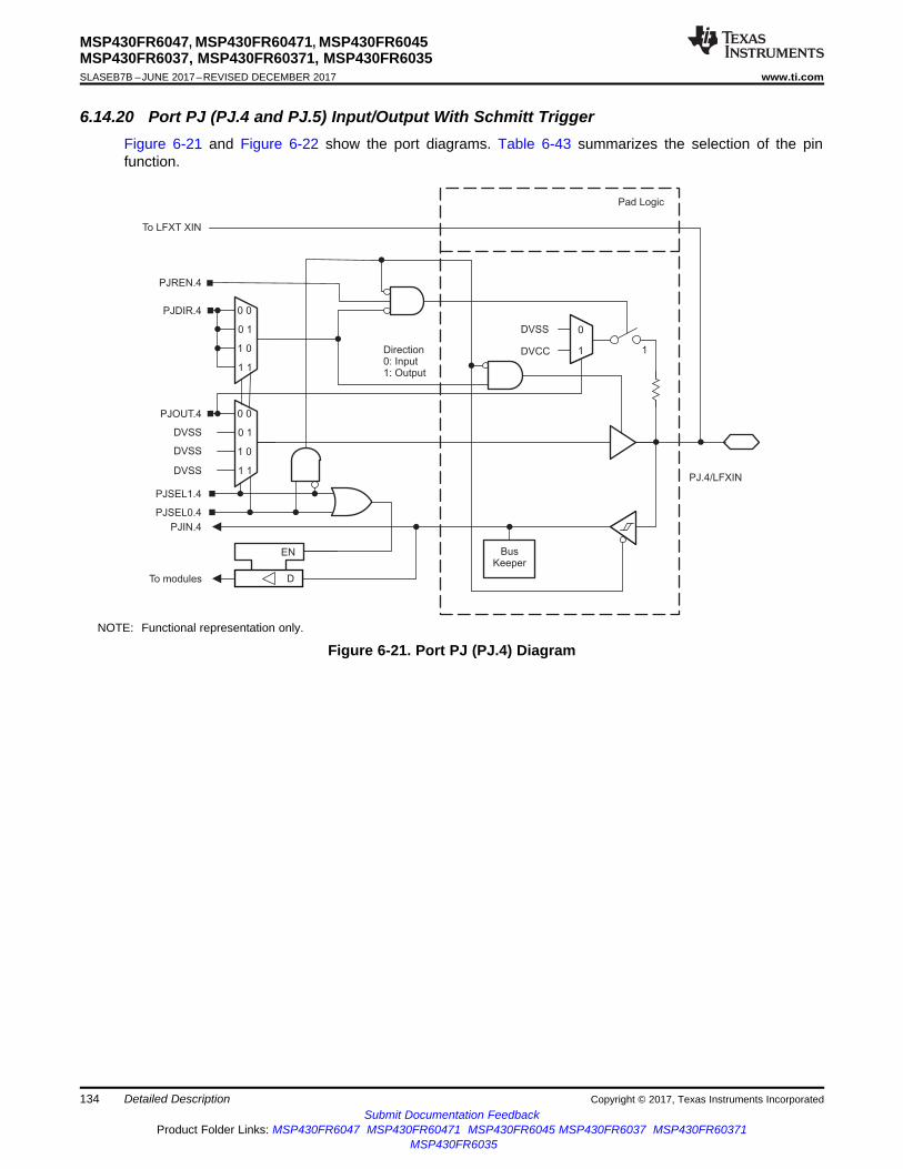
PJ.4/LFXIN
PJSEL1.4
PJDIR.4
PJIN.4
EN
To modules
DVSS
PJOUT.4
1
0DVSS
DVCC 1
D
To LFXT XIN
Pad Logic
BusKeeper
Direction0: Input1: Output
PJREN.4
0 1
0 0
1 0
1 1
PJSEL0.4
0 1
0 0
1 0
1 1
DVSS
DVSS
134
MSP430FR6047, MSP430FR60471, MSP430FR6045MSP430FR6037, MSP430FR60371, MSP430FR6035SLASEB7B –JUNE 2017–REVISED DECEMBER 2017 www.ti.com
Submit Documentation FeedbackProduct Folder Links: MSP430FR6047 MSP430FR60471 MSP430FR6045 MSP430FR6037 MSP430FR60371
MSP430FR6035
Detailed Description Copyright © 2017, Texas Instruments Incorporated
6.14.20 Port PJ (PJ.4 and PJ.5) Input/Output With Schmitt TriggerFigure 6-21 and Figure 6-22 show the port diagrams. Table 6-43 summarizes the selection of the pinfunction.
NOTE: Functional representation only.
Figure 6-21. Port PJ (PJ.4) Diagram

PJ.5/LFXOUT
PJSEL1.5
PJDIR.5
PJIN.5
EN
To modules
DVSS
PJOUT.5
1
0DVSS
DVCC 1
D
To LFXT XOUT
Pad Logic
BusKeeper
Direction0: Input1: Output
PJREN.5
0 1
0 0
1 0
1 1
PJSEL0.5
0 1
0 0
1 0
1 1
DVSS
DVSS
PJSEL1.4
PJSEL0.4
LFXTBYPASS
135
MSP430FR6047, MSP430FR60471, MSP430FR6045MSP430FR6037, MSP430FR60371, MSP430FR6035
www.ti.com SLASEB7B –JUNE 2017–REVISED DECEMBER 2017
Submit Documentation FeedbackProduct Folder Links: MSP430FR6047 MSP430FR60471 MSP430FR6045 MSP430FR6037 MSP430FR60371
MSP430FR6035
Detailed DescriptionCopyright © 2017, Texas Instruments Incorporated
NOTE: Functional representation only.
Figure 6-22. Port PJ (PJ.5) Diagram

136
MSP430FR6047, MSP430FR60471, MSP430FR6045MSP430FR6037, MSP430FR60371, MSP430FR6035SLASEB7B –JUNE 2017–REVISED DECEMBER 2017 www.ti.com
Submit Documentation FeedbackProduct Folder Links: MSP430FR6047 MSP430FR60471 MSP430FR6045 MSP430FR6037 MSP430FR60371
MSP430FR6035
Detailed Description Copyright © 2017, Texas Instruments Incorporated
(1) X = Don't care(2) If PJSEL1.4 = 0 and PJSEL0.4 = 1, the general-purpose I/O is disabled. When LFXTBYPASS = 0, PJ.4 and PJ.5 are configured for
crystal operation and PJSEL1.5 and PJSEL0.5 are don't care. When LFXTBYPASS = 1, PJ.4 is configured for bypass operation andPJ.5 is configured as general-purpose I/O.
(3) When PJ.4 is configured in bypass mode, PJ.5 is configured as general-purpose I/O.(4) If PJSEL0.5 = 1 or PJSEL1.5 = 1, the general-purpose I/O functionality is disabled. No input function is available. Configured as output,
the pin is actively pulled to zero.
Table 6-43. Port PJ (PJ.4 and PJ.5) Pin Functions
PIN NAME (PJ.x) x FUNCTIONCONTROL BITS AND SIGNALS (1)
PJDIR.x PJSEL1.5 PJSEL0.5 PJSEL1.4 PJSEL0.4 LFXTBYPASS
PJ.4/LFXIN 4
PJ.4 (I/O) I: 0; O: 1 X X 0 0 XN/A 0
X X 1 X XInternally tied to DVSS 1LFXIN crystal mode (2) X X X 0 1 0LFXIN bypass mode (2) X X X 0 1 1
PJ.5/LFXOUT 5
PJ.5 (I/O) I: 0; O: 1 0 00 0
01 XX X 1 (3)
N/A 0 see (4) see (4)
0 00
1 XX X 1 (3)
Internally tied to DVSS 1 see (4) see (4)
0 00
1 XX X 1 (3)
LFXOUT crystal mode (2) X X X 0 1 0
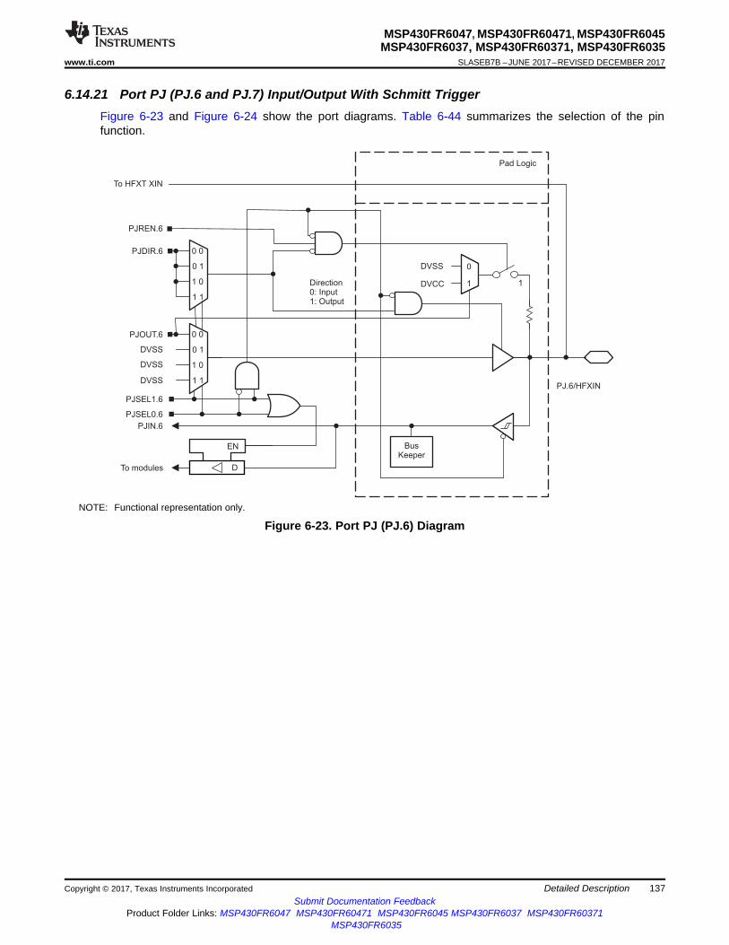
PJ.6/HFXIN
PJSEL1.6
PJDIR.6
PJIN.6
EN
To modules
DVSS
PJOUT.6
1
0DVSS
DVCC 1
D
To HFXT XIN
Pad Logic
BusKeeper
Direction0: Input1: Output
PJREN.6
0 1
0 0
1 0
1 1
PJSEL0.6
0 1
0 0
1 0
1 1
DVSS
DVSS
137
MSP430FR6047, MSP430FR60471, MSP430FR6045MSP430FR6037, MSP430FR60371, MSP430FR6035
www.ti.com SLASEB7B –JUNE 2017–REVISED DECEMBER 2017
Submit Documentation FeedbackProduct Folder Links: MSP430FR6047 MSP430FR60471 MSP430FR6045 MSP430FR6037 MSP430FR60371
MSP430FR6035
Detailed DescriptionCopyright © 2017, Texas Instruments Incorporated
6.14.21 Port PJ (PJ.6 and PJ.7) Input/Output With Schmitt TriggerFigure 6-23 and Figure 6-24 show the port diagrams. Table 6-44 summarizes the selection of the pinfunction.
NOTE: Functional representation only.
Figure 6-23. Port PJ (PJ.6) Diagram
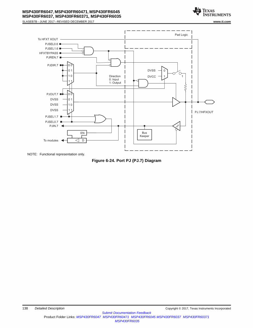
PJ.7/HFXOUT
PJSEL1.7
PJDIR.7
PJIN.7
EN
To modules
DVSS
PJOUT.7
1
0DVSS
DVCC 1
D
To HFXT XOUT
Pad Logic
BusKeeper
Direction0: Input1: Output
PJREN.7
0 1
0 0
1 0
1 1
PJSEL0.7
0 1
0 0
1 0
1 1
DVSS
DVSS
PJSEL1.6
HFXTBYPASS
PJSEL0.6
138
MSP430FR6047, MSP430FR60471, MSP430FR6045MSP430FR6037, MSP430FR60371, MSP430FR6035SLASEB7B –JUNE 2017–REVISED DECEMBER 2017 www.ti.com
Submit Documentation FeedbackProduct Folder Links: MSP430FR6047 MSP430FR60471 MSP430FR6045 MSP430FR6037 MSP430FR60371
MSP430FR6035
Detailed Description Copyright © 2017, Texas Instruments Incorporated
NOTE: Functional representation only.
Figure 6-24. Port PJ (PJ.7) Diagram

139
MSP430FR6047, MSP430FR60471, MSP430FR6045MSP430FR6037, MSP430FR60371, MSP430FR6035
www.ti.com SLASEB7B –JUNE 2017–REVISED DECEMBER 2017
Submit Documentation FeedbackProduct Folder Links: MSP430FR6047 MSP430FR60471 MSP430FR6045 MSP430FR6037 MSP430FR60371
MSP430FR6035
Detailed DescriptionCopyright © 2017, Texas Instruments Incorporated
(1) X = Don't care(2) Setting PJSEL1.6 = 0 and PJSEL0.6 = 1 causes the general-purpose I/O to be disabled. When HFXTBYPASS = 0, PJ.6 and PJ.7 are
configured for crystal operation and PJSEL1.6 and PJSEL0.7 are do not care. When HFXTBYPASS = 1, PJ.6 is configured for bypassoperation and PJ.7 is configured as general-purpose I/O.
(3) With PJSEL0.7 = 1 or PJSEL1.7 =1 the general-purpose I/O functionality is disabled. No input function is available. Configured as outputthe pin is actively pulled to zero.
(4) When PJ.6 is configured in bypass mode, PJ.7 is configured as general-purpose I/O.
Table 6-44. Port PJ (PJ.6 and PJ.7) Pin Functions
PIN NAME (PJ.x) x FUNCTIONCONTROL BITS AND SIGNALS (1)
PJDIR.x PJSEL1.7 PJSEL0.7 PJSEL1.6 PJSEL0.6 HFXTBYPASS
PJ.6/HFXIN 6
PJ.6 (I/O) I: 0; O: 1 X X 0 0 XN/A 0
X X 1 X XInternally tied to DVSS 1HFXIN crystal mode (2) X X X 0 1 0HFXIN bypass mode (2) X X X 0 1 1
PJ.7/HFXOUT 7
PJ.7 (I/O) (3) I: 0; O: 1 0 00 0
01 XX X 1 (4)
N/A 0 see (3) see (3)
0 00
1 XX X 1 (4)
Internally tied to DVSS 1 see (3) see (3)
0 00
1 XX X 1 (4)
HFXOUT crystal mode (2) X X X 0 1 0
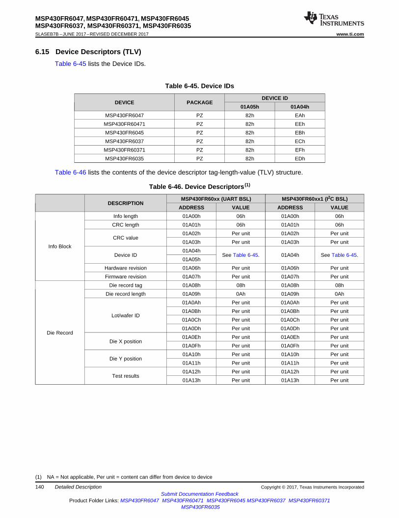
140
MSP430FR6047, MSP430FR60471, MSP430FR6045MSP430FR6037, MSP430FR60371, MSP430FR6035SLASEB7B –JUNE 2017–REVISED DECEMBER 2017 www.ti.com
Submit Documentation FeedbackProduct Folder Links: MSP430FR6047 MSP430FR60471 MSP430FR6045 MSP430FR6037 MSP430FR60371
MSP430FR6035
Detailed Description Copyright © 2017, Texas Instruments Incorporated
6.15 Device Descriptors (TLV)Table 6-45 lists the Device IDs.
Table 6-45. Device IDs
DEVICE PACKAGEDEVICE ID
01A05h 01A04hMSP430FR6047 PZ 82h EAhMSP430FR60471 PZ 82h EEhMSP430FR6045 PZ 82h EBhMSP430FR6037 PZ 82h EChMSP430FR60371 PZ 82h EFhMSP430FR6035 PZ 82h EDh
(1) NA = Not applicable, Per unit = content can differ from device to device
Table 6-46 lists the contents of the device descriptor tag-length-value (TLV) structure.
Table 6-46. Device Descriptors (1)
DESCRIPTIONMSP430FR60xx (UART BSL) MSP430FR60xx1 (I2C BSL)
ADDRESS VALUE ADDRESS VALUE
Info Block
Info length 01A00h 06h 01A00h 06hCRC length 01A01h 06h 01A01h 06h
CRC value01A02h Per unit 01A02h Per unit01A03h Per unit 01A03h Per unit
Device ID01A04h
See Table 6-45. 01A04h See Table 6-45.01A05h
Hardware revision 01A06h Per unit 01A06h Per unitFirmware revision 01A07h Per unit 01A07h Per unit
Die Record
Die record tag 01A08h 08h 01A08h 08hDie record length 01A09h 0Ah 01A09h 0Ah
Lot/wafer ID
01A0Ah Per unit 01A0Ah Per unit01A0Bh Per unit 01A0Bh Per unit01A0Ch Per unit 01A0Ch Per unit01A0Dh Per unit 01A0Dh Per unit
Die X position01A0Eh Per unit 01A0Eh Per unit01A0Fh Per unit 01A0Fh Per unit
Die Y position01A10h Per unit 01A10h Per unit01A11h Per unit 01A11h Per unit
Test results01A12h Per unit 01A12h Per unit01A13h Per unit 01A13h Per unit
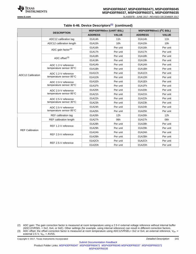
141
MSP430FR6047, MSP430FR60471, MSP430FR6045MSP430FR6037, MSP430FR60371, MSP430FR6035
www.ti.com SLASEB7B –JUNE 2017–REVISED DECEMBER 2017
Submit Documentation FeedbackProduct Folder Links: MSP430FR6047 MSP430FR60471 MSP430FR6045 MSP430FR6037 MSP430FR60371
MSP430FR6035
Detailed DescriptionCopyright © 2017, Texas Instruments Incorporated
Table 6-46. Device Descriptors(1) (continued)
DESCRIPTIONMSP430FR60xx (UART BSL) MSP430FR60xx1 (I2C BSL)
ADDRESS VALUE ADDRESS VALUE
(2) ADC gain: The gain correction factor is measured at room temperature using a 2.5-V external voltage reference without internal buffer(ADC12VRSEL = 0x2, 0x4, or 0xE). Other settings (for example, using internal reference) can result in different correction factors.
(3) ADC offset: the offset correction factor is measured at room temperature using ADC12VRSEL= 0x2 or 0x4, an external reference, VR+ =external 2.5 V, VR– = AVSS.
ADC12 Calibration
ADC12 calibration tag 01A14h 11h 01A14h 11hADC12 calibration length 01A15h 10h 01A15h 10h
ADC gain factor (2) 01A16h Per unit 01A16h Per unit01A17h Per unit 01A17h Per unit
ADC offset (3) 01A18h Per unit 01A18h Per unit01A19h Per unit 01A19h Per unit
ADC 1.2-V referencetemperature sensor 30°C
01A1Ah Per unit 01A1Ah Per unit01A1Bh Per unit 01A1Bh Per unit
ADC 1.2-V referencetemperature sensor 85°C
01A1Ch Per unit 01A1Ch Per unit01A1Dh Per unit 01A1Dh Per unit
ADC 2.0-V referencetemperature sensor 30°C
01A1Eh Per unit 01A1Eh Per unit01A1Fh Per unit 01A1Fh Per unit
ADC 2.0-V referencetemperature sensor 85°C
01A20h Per unit 01A20h Per unit01A21h Per unit 01A21h Per unit
ADC 2.5-V referencetemperature sensor 30°C
01A22h Per unit 01A22h Per unit01A23h Per unit 01A23h Per unit
ADC 2.5-V referencetemperature sensor 85°C
01A24h Per unit 01A24h Per unit01A25h Per unit 01A25h Per unit
REF Calibration
REF calibration tag 01A26h 12h 01A26h 12hREF calibration length 01A27h 06h 01A27h 06h
REF 1.2-V reference01A28h Per unit 01A28h Per unit01A29h Per unit 01A29h Per unit
REF 2.0-V reference01A2Ah Per unit 01A2Ah Per unit01A2Bh Per unit 01A2Bh Per unit
REF 2.5-V reference01A2Ch Per unit 01A2Ch Per unit01A2Dh Per unit 01A2Dh Per unit

142
MSP430FR6047, MSP430FR60471, MSP430FR6045MSP430FR6037, MSP430FR60371, MSP430FR6035SLASEB7B –JUNE 2017–REVISED DECEMBER 2017 www.ti.com
Submit Documentation FeedbackProduct Folder Links: MSP430FR6047 MSP430FR60471 MSP430FR6045 MSP430FR6037 MSP430FR60371
MSP430FR6035
Detailed Description Copyright © 2017, Texas Instruments Incorporated
Table 6-46. Device Descriptors(1) (continued)
DESCRIPTIONMSP430FR60xx (UART BSL) MSP430FR60xx1 (I2C BSL)
ADDRESS VALUE ADDRESS VALUE
(4) 128-bit random number: The random number is generated during production test using the Microsoft® CryptGenRandom() function.
Random Number
128-bit random number tag 01A2Eh 15h 01A2Eh 15hRandom number length 01A2Fh 10h 01A2Fh 10h
128-bit random number (4)
01A30h Per unit 01A30h Per unit01A31h Per unit 01A31h Per unit01A32h Per unit 01A32h Per unit01A33h Per unit 01A33h Per unit01A34h Per unit 01A34h Per unit01A35h Per unit 01A35h Per unit01A36h Per unit 01A36h Per unit01A37h Per unit 01A37h Per unit01A38h Per unit 01A38h Per unit01A39h Per unit 01A39h Per unit01A3Ah Per unit 01A3Ah Per unit01A3Bh Per unit 01A3Bh Per unit01A3Ch Per unit 01A3Ch Per unit01A3Dh Per unit 01A3Dh Per unit01A3Eh Per unit 01A3Eh Per unit01A3Fh Per unit 01A3Fh Per unit
BSL Configuration
BSL tag 01A40h 1Ch 01A40h 1ChBSL length 01A41h 02h 01A41h 02h
BSL interface 01A42h 00h 01A42h 01hBSL interface configuration 01A43h 00h 01A43h 48h

143
MSP430FR6047, MSP430FR60471, MSP430FR6045MSP430FR6037, MSP430FR60371, MSP430FR6035
www.ti.com SLASEB7B –JUNE 2017–REVISED DECEMBER 2017
Submit Documentation FeedbackProduct Folder Links: MSP430FR6047 MSP430FR60471 MSP430FR6045 MSP430FR6037 MSP430FR60371
MSP430FR6035
Detailed DescriptionCopyright © 2017, Texas Instruments Incorporated
(1) All address space not listed is considered vacant memory.
6.16 Memory MapTable 6-47 summarizes the memory organization for all device variants.
Table 6-47. Memory Organization (1)
MSP430FR6047(1), FR6037(1) MSP430FR6045, FR6035Memory (FRAM)Main: interrupt vectors andsignaturesMain: code memory
Total Size 256KB00FFFFh to 00FF80h043FFFh to 004000h
128KB00FFFFh to 00FF80h0023FFFh to 004000h
RAM (shared with LEA)(Sector 2)Block 0
Size 4KB(003BFFh to 002C00h)003BFFh to 002C00h
4KB(003BFFh to 002C00h)003BFFh to 002C00h
System RAM(Sector 1)(Sector 0)Main: base locationMain: interrupt vectors
Size 4KB(002BFFh to 002400h)(0023FFh to 001C00h)002BFFh to 001C00h002BFFh to 002B80h
4KB(002BFFh to 002400h)(0023FFh to 001C00h)002BFFh to 001C00h002BFFh to 002B80h
Device descriptor info (TLV)(FRAM)
Size 256 B001AFFh to 001A00h
256 B001AFFh to 001A00h
TI calibration and configuration(FRAM)
Size 256 B0019FFh to 001900h
256 B0019FFh to 001900h
Bootloader (BSL) memory (ROM)
BSL 3 512 B0017FFh to 001600h
512 B0017FFh to 001600h
BSL 2 512 B0015FFh to 001400h
512 B0015FFh to 001400h
BSL 1 512 B0013FFh to 001200h
512 B0013FFh to 001200h
BSL 0 512 B0011FFh to 001000h
512 B0011FFh to 001000h
Peripherals Size 4KB000FFFh to 000020h
4KB000FFFh to 000020h
Tiny RAM Size 22 B000001Fh to 00000Ah
22 B000001Fh to 00000Ah
Reserved Size 10 B000009h to 000000h
10 B000009h to 000000h

144
MSP430FR6047, MSP430FR60471, MSP430FR6045MSP430FR6037, MSP430FR60371, MSP430FR6035SLASEB7B –JUNE 2017–REVISED DECEMBER 2017 www.ti.com
Submit Documentation FeedbackProduct Folder Links: MSP430FR6047 MSP430FR60471 MSP430FR6045 MSP430FR6037 MSP430FR60371
MSP430FR6035
Detailed Description Copyright © 2017, Texas Instruments Incorporated
6.16.1 Peripheral File MapFor complete module register descriptions, see the MSP430FR58xx, MSP430FR59xx, and MSP430FR6xxFamily User's Guide. Table 6-48 lists the base and end addresses of the registers for each peripheral.
(1) Not available in MSP430FR6037, MSP430FR6035, and MSP430FR60371
Table 6-48. Peripherals
MODULE NAME BASE ADDRESS END ADDRESSSpecial Functions (see Table 6-49) 0100h 011Fh
PMM (see Table 6-50) 0120h 013FhFRAM Control (see Table 6-51) 0140h 014Fh
CRC (see Table 6-52) 0150h 0157hRAM Control (see Table 6-53) 0158h 0159h
Watchdog (see Table 6-54) 015Ch 015DhCS (see Table 6-55) 0160h 016Fh
SYS (see Table 6-56) 0180h 019FhShared Reference (see Table 6-57) 01B0h 01B1h
Digital I/O (see Table 6-58) 0200h 033FhTA0 (see Table 6-59) 0340h 036FhTA1 (see Table 6-60) 0380h 03AFhTB0 (see Table 6-61) 03C0h 03EFhTA2 (see Table 6-62) 0400h 042FhTA3 (see Table 6-63) 0440h 046Fh
RTC_C (see Table 6-64) 04A0h 04BFh32-Bit Hardware Multiplier (see Table 6-65) 04C0h 04EFh
DMA (see Table 6-66) 0500h 056FhMPU Control (see Table 6-67) 05A0h 05AFheUSCI_A0 (see Table 6-68) 05C0h 05DFheUSCI_A1 (see Table 6-69) 05E0h 05FFheUSCI_A2 (see Table 6-70) 0600h 061FheUSCI_A3 (see Table 6-71) 0620h 063FheUSCI_B0 (see Table 6-72) 0640h 066FheUSCI_B1 (see Table 6-73) 0680h 06AFh
TA4 (see Table 6-74) 07C0h 07EFhADC12_B (see Table 6-75) 0800h 089Fh
Comparator E (see Table 6-76) 08C0h 08CFhCRC32 (see Table 6-77) 0980h 09AFhAES256 (see Table 6-78) 09C0h 09CFhLCD_C (see Table 6-79) 0A00h 0A5Fh
LEA (see Table 6-80) 0A80h 0AFFhSAPH (1) (see Table 6-81) 0E00h 0E7FhSDHS (1) (see Table 6-82) 0E80h 0EBFhUUPS (1) (see Table 6-83) 0EC0h 0EDFhHSPLL (1) (see Table 6-84) 0EE0h 0EFFh
MTIF (see Table 6-85) 0F00h 0F1Fh
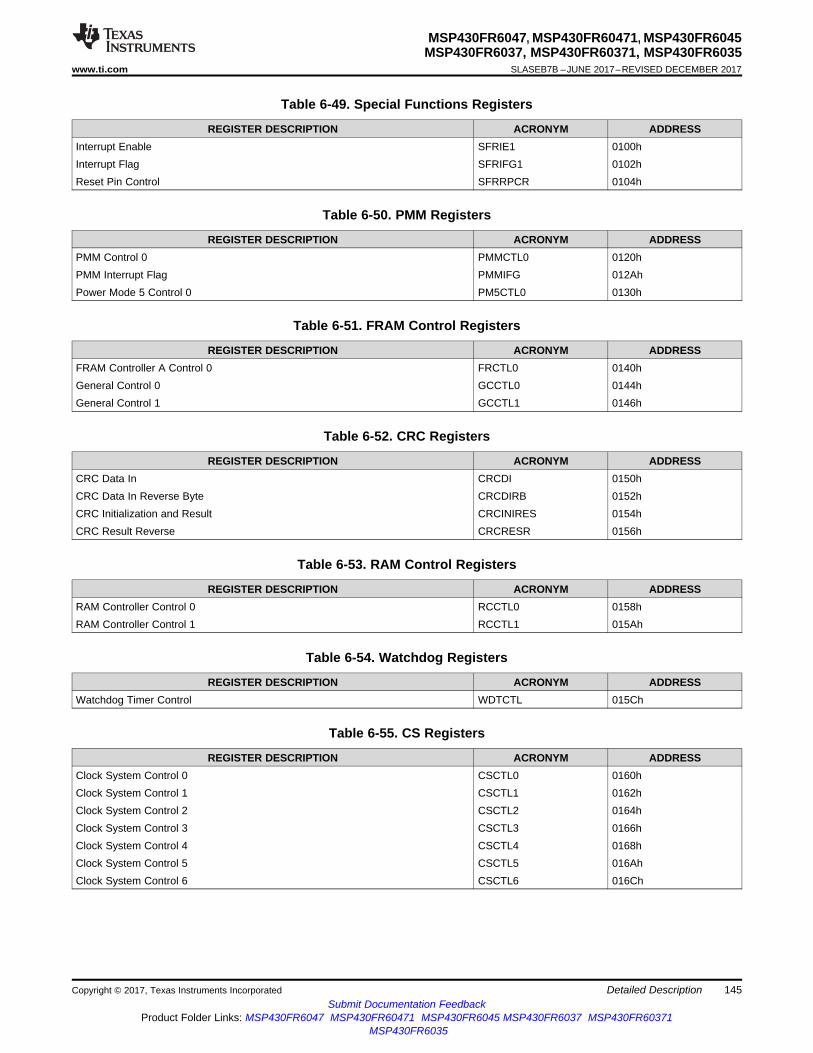
145
MSP430FR6047, MSP430FR60471, MSP430FR6045MSP430FR6037, MSP430FR60371, MSP430FR6035
www.ti.com SLASEB7B –JUNE 2017–REVISED DECEMBER 2017
Submit Documentation FeedbackProduct Folder Links: MSP430FR6047 MSP430FR60471 MSP430FR6045 MSP430FR6037 MSP430FR60371
MSP430FR6035
Detailed DescriptionCopyright © 2017, Texas Instruments Incorporated
Table 6-49. Special Functions Registers
REGISTER DESCRIPTION ACRONYM ADDRESSInterrupt Enable SFRIE1 0100hInterrupt Flag SFRIFG1 0102hReset Pin Control SFRRPCR 0104h
Table 6-50. PMM Registers
REGISTER DESCRIPTION ACRONYM ADDRESSPMM Control 0 PMMCTL0 0120hPMM Interrupt Flag PMMIFG 012AhPower Mode 5 Control 0 PM5CTL0 0130h
Table 6-51. FRAM Control Registers
REGISTER DESCRIPTION ACRONYM ADDRESSFRAM Controller A Control 0 FRCTL0 0140hGeneral Control 0 GCCTL0 0144hGeneral Control 1 GCCTL1 0146h
Table 6-52. CRC Registers
REGISTER DESCRIPTION ACRONYM ADDRESSCRC Data In CRCDI 0150hCRC Data In Reverse Byte CRCDIRB 0152hCRC Initialization and Result CRCINIRES 0154hCRC Result Reverse CRCRESR 0156h
Table 6-53. RAM Control Registers
REGISTER DESCRIPTION ACRONYM ADDRESSRAM Controller Control 0 RCCTL0 0158hRAM Controller Control 1 RCCTL1 015Ah
Table 6-54. Watchdog Registers
REGISTER DESCRIPTION ACRONYM ADDRESSWatchdog Timer Control WDTCTL 015Ch
Table 6-55. CS Registers
REGISTER DESCRIPTION ACRONYM ADDRESSClock System Control 0 CSCTL0 0160hClock System Control 1 CSCTL1 0162hClock System Control 2 CSCTL2 0164hClock System Control 3 CSCTL3 0166hClock System Control 4 CSCTL4 0168hClock System Control 5 CSCTL5 016AhClock System Control 6 CSCTL6 016Ch
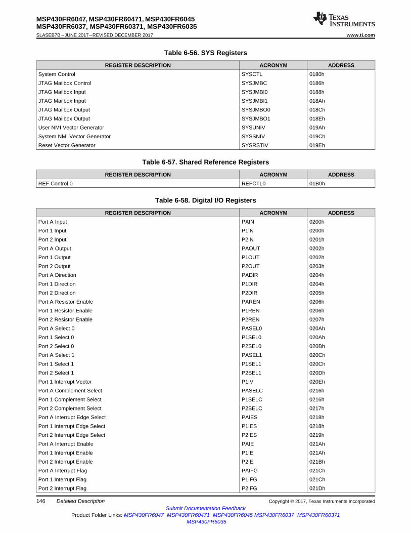
146
MSP430FR6047, MSP430FR60471, MSP430FR6045MSP430FR6037, MSP430FR60371, MSP430FR6035SLASEB7B –JUNE 2017–REVISED DECEMBER 2017 www.ti.com
Submit Documentation FeedbackProduct Folder Links: MSP430FR6047 MSP430FR60471 MSP430FR6045 MSP430FR6037 MSP430FR60371
MSP430FR6035
Detailed Description Copyright © 2017, Texas Instruments Incorporated
Table 6-56. SYS Registers
REGISTER DESCRIPTION ACRONYM ADDRESSSystem Control SYSCTL 0180hJTAG Mailbox Control SYSJMBC 0186hJTAG Mailbox Input SYSJMBI0 0188hJTAG Mailbox Input SYSJMBI1 018AhJTAG Mailbox Output SYSJMBO0 018ChJTAG Mailbox Output SYSJMBO1 018EhUser NMI Vector Generator SYSUNIV 019AhSystem NMI Vector Generator SYSSNIV 019ChReset Vector Generator SYSRSTIV 019Eh
Table 6-57. Shared Reference Registers
REGISTER DESCRIPTION ACRONYM ADDRESSREF Control 0 REFCTL0 01B0h
Table 6-58. Digital I/O Registers
REGISTER DESCRIPTION ACRONYM ADDRESSPort A Input PAIN 0200hPort 1 Input P1IN 0200hPort 2 Input P2IN 0201hPort A Output PAOUT 0202hPort 1 Output P1OUT 0202hPort 2 Output P2OUT 0203hPort A Direction PADIR 0204hPort 1 Direction P1DIR 0204hPort 2 Direction P2DIR 0205hPort A Resistor Enable PAREN 0206hPort 1 Resistor Enable P1REN 0206hPort 2 Resistor Enable P2REN 0207hPort A Select 0 PASEL0 020AhPort 1 Select 0 P1SEL0 020AhPort 2 Select 0 P2SEL0 020BhPort A Select 1 PASEL1 020ChPort 1 Select 1 P1SEL1 020ChPort 2 Select 1 P2SEL1 020DhPort 1 Interrupt Vector P1IV 020EhPort A Complement Select PASELC 0216hPort 1 Complement Select P1SELC 0216hPort 2 Complement Select P2SELC 0217hPort A Interrupt Edge Select PAIES 0218hPort 1 Interrupt Edge Select P1IES 0218hPort 2 Interrupt Edge Select P2IES 0219hPort A Interrupt Enable PAIE 021AhPort 1 Interrupt Enable P1IE 021AhPort 2 Interrupt Enable P2IE 021BhPort A Interrupt Flag PAIFG 021ChPort 1 Interrupt Flag P1IFG 021ChPort 2 Interrupt Flag P2IFG 021Dh
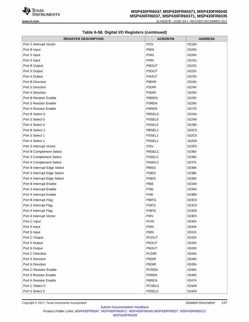
147
MSP430FR6047, MSP430FR60471, MSP430FR6045MSP430FR6037, MSP430FR60371, MSP430FR6035
www.ti.com SLASEB7B –JUNE 2017–REVISED DECEMBER 2017
Submit Documentation FeedbackProduct Folder Links: MSP430FR6047 MSP430FR60471 MSP430FR6045 MSP430FR6037 MSP430FR60371
MSP430FR6035
Detailed DescriptionCopyright © 2017, Texas Instruments Incorporated
Table 6-58. Digital I/O Registers (continued)REGISTER DESCRIPTION ACRONYM ADDRESS
Port 2 Interrupt Vector P2IV 021EhPort B Input PBIN 0220hPort 3 Input P3IN 0220hPort 4 Input P4IN 0221hPort B Output PBOUT 0222hPort 3 Output P3OUT 0222hPort 4 Output P4OUT 0223hPort B Direction PBDIR 0224hPort 3 Direction P3DIR 0224hPort 4 Direction P4DIR 0225hPort B Resistor Enable PBREN 0226hPort 3 Resistor Enable P3REN 0226hPort 4 Resistor Enable P4REN 0227hPort B Select 0 PBSEL0 022AhPort 3 Select 0 P3SEL0 022AhPort 4 Select 0 P4SEL0 022BhPort B Select 1 PBSEL1 022ChPort 3 Select 1 P3SEL1 022ChPort 4 Select 1 P4SEL1 022DhPort 3 Interrupt Vector P3IV 022EhPort B Complement Select PBSELC 0236hPort 3 Complement Select P3SELC 0236hPort 4 Complement Select P4SELC 0237hPort B Interrupt Edge Select PBIES 0238hPort 3 Interrupt Edge Select P3IES 0238hPort 4 Interrupt Edge Select P4IES 0239hPort B Interrupt Enable PBIE 023AhPort 3 Interrupt Enable P3IE 023AhPort 4 Interrupt Enable P4IE 023BhPort B Interrupt Flag PBIFG 023ChPort 3 Interrupt Flag P3IFG 023ChPort 4 Interrupt Flag P4IFG 023DhPort 4 Interrupt Vector P4IV 023EhPort C Input PCIN 0240hPort 5 Input P5IN 0240hPort 6 Input P6IN 0241hPort C Output PCOUT 0242hPort 5 Output P5OUT 0242hPort 6 Output P6OUT 0243hPort C Direction PCDIR 0244hPort 5 Direction P5DIR 0244hPort 6 Direction P6DIR 0245hPort C Resistor Enable PCREN 0246hPort 5 Resistor Enable P5REN 0246hPort 6 Resistor Enable P6REN 0247hPort C Select 0 PCSEL0 024AhPort 5 Select 0 P5SEL0 024Ah

148
MSP430FR6047, MSP430FR60471, MSP430FR6045MSP430FR6037, MSP430FR60371, MSP430FR6035SLASEB7B –JUNE 2017–REVISED DECEMBER 2017 www.ti.com
Submit Documentation FeedbackProduct Folder Links: MSP430FR6047 MSP430FR60471 MSP430FR6045 MSP430FR6037 MSP430FR60371
MSP430FR6035
Detailed Description Copyright © 2017, Texas Instruments Incorporated
Table 6-58. Digital I/O Registers (continued)REGISTER DESCRIPTION ACRONYM ADDRESS
Port 6 Select 0 P6SEL0 024BhPort C Select 1 PCSEL1 024ChPort 5 Select 1 P5SEL1 024ChPort 6 Select 1 P6SEL1 024DhPort 5 Interrupt Vector P5IV 024EhPort C Complement Select PCSELC 0256hPort 5 Complement Select P5SELC 0256hPort 6 Complement Select P6SELC 0257hPort C Interrupt Edge Select PCIES 0258hPort 5 Interrupt Edge Select P5IES 0258hPort 6 Interrupt Edge Select P6IES 0259hPort C Interrupt Enable PCIE 025AhPort 5 Interrupt Enable P5IE 025AhPort 6 Interrupt Enable P6IE 025BhPort C Interrupt Flag PCIFG 025ChPort 5 Interrupt Flag P5IFG 025ChPort 6 Interrupt Flag P6IFG 025DhPort 6 Interrupt Vector P6IV 025EhPort D Input PDIN 0260hPort 7 Input P7IN 0260hPort 8 Input P8IN 0261hPort D Output PDOUT 0262hPort 7 Output P7OUT 0262hPort 8 Output P8OUT 0263hPort D Direction PDDIR 0264hPort 7 Direction P7DIR 0264hPort 8 Direction P8DIR 0265hPort D Resistor Enable PDREN 0266hPort 7 Resistor Enable P7REN 0266hPort 8 Resistor Enable P8REN 0267hPort D Select 0 PDSEL0 026AhPort 7 Select 0 P7SEL0 026AhPort 8 Select 0 P8SEL0 026BhPort D Select 1 PDSEL1 026ChPort 7 Select 1 P7SEL1 026ChPort 8 Select 1 P8SEL1 026DhPort 7 Interrupt Vector P7IV 026EhPort D Complement Select PDSELC 0276hPort 7 Complement Select P7SELC 0276hPort 8 Complement Select P8SELC 0277hPort D Interrupt Edge Select PDIES 0278hPort 7 Interrupt Edge Select P7IES 0278hPort 8 Interrupt Edge Select P8IES 0279hPort D Interrupt Enable PDIE 027AhPort 7 Interrupt Enable P7IE 027AhPort 8 Interrupt Enable P8IE 027BhPort D Interrupt Flag PDIFG 027Ch
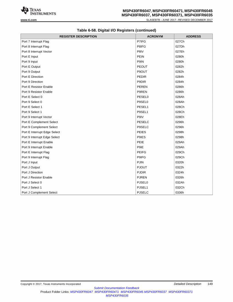
149
MSP430FR6047, MSP430FR60471, MSP430FR6045MSP430FR6037, MSP430FR60371, MSP430FR6035
www.ti.com SLASEB7B –JUNE 2017–REVISED DECEMBER 2017
Submit Documentation FeedbackProduct Folder Links: MSP430FR6047 MSP430FR60471 MSP430FR6045 MSP430FR6037 MSP430FR60371
MSP430FR6035
Detailed DescriptionCopyright © 2017, Texas Instruments Incorporated
Table 6-58. Digital I/O Registers (continued)REGISTER DESCRIPTION ACRONYM ADDRESS
Port 7 Interrupt Flag P7IFG 027ChPort 8 Interrupt Flag P8IFG 027DhPort 8 Interrupt Vector P8IV 027EhPort E Input PEIN 0280hPort 9 Input P9IN 0280hPort E Output PEOUT 0282hPort 9 Output P9OUT 0282hPort E Direction PEDIR 0284hPort 9 Direction P9DIR 0284hPort E Resistor Enable PEREN 0286hPort 9 Resistor Enable P9REN 0286hPort E Select 0 PESEL0 028AhPort 9 Select 0 P9SEL0 028AhPort E Select 1 PESEL1 028ChPort 9 Select 1 P9SEL1 028ChPort 9 Interrupt Vector P9IV 028EhPort E Complement Select PESELC 0296hPort 9 Complement Select P9SELC 0296hPort E Interrupt Edge Select PEIES 0298hPort 9 Interrupt Edge Select P9IES 0298hPort E Interrupt Enable PEIE 029AhPort 9 Interrupt Enable P9IE 029AhPort E Interrupt Flag PEIFG 029ChPort 9 Interrupt Flag P9IFG 029ChPort J Input PJIN 0320hPort J Output PJOUT 0322hPort J Direction PJDIR 0324hPort J Resistor Enable PJREN 0326hPort J Select 0 PJSEL0 032AhPort J Select 1 PJSEL1 032ChPort J Complement Select PJSELC 0336h

150
MSP430FR6047, MSP430FR60471, MSP430FR6045MSP430FR6037, MSP430FR60371, MSP430FR6035SLASEB7B –JUNE 2017–REVISED DECEMBER 2017 www.ti.com
Submit Documentation FeedbackProduct Folder Links: MSP430FR6047 MSP430FR60471 MSP430FR6045 MSP430FR6037 MSP430FR60371
MSP430FR6035
Detailed Description Copyright © 2017, Texas Instruments Incorporated
Table 6-59. TA0 Registers
REGISTER DESCRIPTION ACRONYM ADDRESSTimer_A0 Control TA0CTL 0340hTimer_A0 Capture/Compare Control TA0CCTL0 0342hTimer_A0 Capture/Compare Control TA0CCTL1 0344hTimer_A0 Capture/Compare Control TA0CCTL2 0346hTimer_A0 Counter TA0R 0350hTimer_A0 Capture/Compare TA0CCR0 0352hTimer_A0 Capture/Compare TA0CCR1 0354hTimer_A0 Capture/Compare TA0CCR2 0356hTimer_A0 Expansion 0 TA0EX0 0360hTimer_A0 Interrupt Vector TA0IV 036Eh
Table 6-60. TA1 Registers
REGISTER DESCRIPTION ACRONYM ADDRESSTimer_A1 Control TA1CTL 0380hTimer_A1 Capture/Compare Control TA1CCTL0 0382hTimer_A1 Capture/Compare Control TA1CCTL1 0384hTimer_A1 Capture/Compare Control TA1CCTL2 0386hTimer_A1 Counter TA1R 0390hTimer_A1 Capture/Compare TA1CCR0 0392hTimer_A1 Capture/Compare TA1CCR1 0394hTimer_A1 Capture/Compare TA1CCR2 0396hTimer_A1 Expansion 0 TA1EX0 03A0hTimer_A1 Interrupt Vector TA1IV 03AEh
Table 6-61. TB0 Registers
REGISTER DESCRIPTION ACRONYM ADDRESSTimer_B0 Control TB0CTL 03C0hTimer_B0 Capture/Compare Control TB0CCTL0 03C2hTimer_B0 Capture/Compare Control TB0CCTL1 03C4hTimer_B0 Capture/Compare Control TB0CCTL2 03C6hTimer_B0 Capture/Compare Control TB0CCTL3 03C8hTimer_B0 Capture/Compare Control TB0CCTL4 03CAhTimer_B0 Capture/Compare Control TB0CCTL5 03CChTimer_B0 Capture/Compare Control TB0CCTL6 03CEhTimer_B0 Counter TB0R 03D0hTimer_B0 Capture/Compare TB0CCR0 03D2hTimer_B0 Capture/Compare TB0CCR1 03D4hTimer_B0 Capture/Compare TB0CCR2 03D6hTimer_B0 Capture/Compare TB0CCR3 03D8hTimer_B0 Capture/Compare TB0CCR4 03DAhTimer_B0 Capture/Compare TB0CCR5 03DChTimer_B0 Capture/Compare TB0CCR6 03DEhTimer_B0 Expansion 0 TB0EX0 03E0hTimer_B0 Interrupt Vector TB0IV 03EEh

151
MSP430FR6047, MSP430FR60471, MSP430FR6045MSP430FR6037, MSP430FR60371, MSP430FR6035
www.ti.com SLASEB7B –JUNE 2017–REVISED DECEMBER 2017
Submit Documentation FeedbackProduct Folder Links: MSP430FR6047 MSP430FR60471 MSP430FR6045 MSP430FR6037 MSP430FR60371
MSP430FR6035
Detailed DescriptionCopyright © 2017, Texas Instruments Incorporated
Table 6-62. TA2 Registers
REGISTER DESCRIPTION ACRONYM ADDRESSTimer_A2 Control TA2CTL 0400hTimer_A2 Capture/Compare Control TA2CCTL0 0402hTimer_A2 Capture/Compare Control TA2CCTL1 0404hTimer_A2 Counter TA2R 0410hTimer_A2 Capture/Compare TA2CCR0 0412hTimer_A2 Capture/Compare TA2CCR1 0414hTimer_A2 Expansion 0 TA2EX0 0420hTimer_A2 Interrupt Vector TA2IV 042Eh
Table 6-63. TA3 Registers
REGISTER DESCRIPTION ACRONYM ADDRESSTimer_A3 Control TA3CTL 0440hTimer_A3 Capture/Compare Control TA3CCTL0 0442hTimer_A3 Capture/Compare Control TA3CCTL1 0444hTimer_A3 Counter TA3R 0450hTimer_A3 Capture/Compare TA3CCR0 0452hTimer_A3 Capture/Compare TA3CCR1 0454hTimer_A3 Expansion 0 TA3EX0 0460hTimer_A3 Interrupt Vector TA3IV 046Eh
Table 6-64. RTC_C Registers
REGISTER DESCRIPTION ACRONYM ADDRESSReal-Time Clock Control 0 RTCCTL0 04A0hReal-Time Clock Control 1, 3 RTCCTL13 04A2hReal-Time Clock Offset Calibration RTCOCAL 04A4hReal-Time Clock Temperature Compensation RTCTCMP 04A6hReal-Time Clock Prescale Timer 0 Control RTCPS0CTL 04A8hReal-Time Clock Prescale Timer 1 Control RTCPS1CTL 04AAhReal-Time Clock Prescale Timer Counter RTCPS 04AChPrescale Timer 0 Counter Value RT0PS 04AChPrescale Timer 1 Counter Value RT1PS 04ADhReal-Time Clock Interrupt Vector RTCIV 04AEhReal-Time Clock Seconds and Minutes RTCTIM0 04B0hReal-Time Clock Hour, Day of Week RTCTIM1 04B2hReal-Time Clock Date RTCDATE 04B4hReal-Time Clock Year RTCYEAR 04B6hReal-Time Clock Minute and Hour RTCAMINHR 04B8hReal-Time Clock Alarm Day of Week and Day RTCADOWDAY 04BAhBinary-to-BCD Conversion BIN2BCD 04BChBCD-to-Binary Conversion BCD2BIN 04BEh
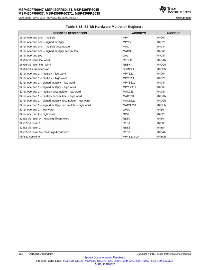
152
MSP430FR6047, MSP430FR60471, MSP430FR6045MSP430FR6037, MSP430FR60371, MSP430FR6035SLASEB7B –JUNE 2017–REVISED DECEMBER 2017 www.ti.com
Submit Documentation FeedbackProduct Folder Links: MSP430FR6047 MSP430FR60471 MSP430FR6045 MSP430FR6037 MSP430FR60371
MSP430FR6035
Detailed Description Copyright © 2017, Texas Instruments Incorporated
Table 6-65. 32-Bit Hardware Multiplier Registers
REGISTER DESCRIPTION ACRONYM ADDRESS16-bit operand one – multiply MPY 04C0h16-bit operand one – signed multiply MPYS 04C2h16-bit operand one – multiply accumulate MAC 04C4h16-bit operand one – signed multiply accumulate MACS 04C6h16-bit operand two OP2 04C8h16x16-bit result low word RESLO 04CAh16x16-bit result high word RESHI 04CCh16x16-bit sum extension SUMEXT 04CEh32-bit operand 1 – multiply – low word MPY32L 04D0h32-bit operand 1 – multiply – high word MPY32H 04D2h32-bit operand 1 – signed multiply – low word MPYS32L 04D4h32-bit operand 1 – signed multiply – high word MPYS32H 04D6h32-bit operand 1 – multiply accumulate – low word MAC32L 04D8h32-bit operand 1 – multiply accumulate – high word MAC32H 04DAh32-bit operand 1 – signed multiply accumulate – low word MACS32L 04DCh32-bit operand 1 – signed multiply accumulate – high word MACS32H 04DEh32-bit operand 2 – low word OP2L 04E0h32-bit operand 2 – high word OP2H 04E2h32x32-bit result 0 – least significant word RES0 04E4h32x32-bit result 1 RES1 04E6h32x32-bit result 2 RES2 04E8h32x32-bit result 3 – most significant word RES3 04EAhMPY32 control 0 MPY32CTL0 04ECh
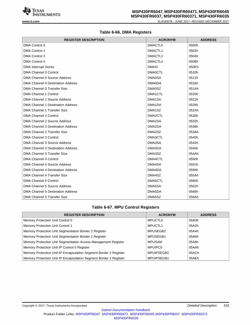
153
MSP430FR6047, MSP430FR60471, MSP430FR6045MSP430FR6037, MSP430FR60371, MSP430FR6035
www.ti.com SLASEB7B –JUNE 2017–REVISED DECEMBER 2017
Submit Documentation FeedbackProduct Folder Links: MSP430FR6047 MSP430FR60471 MSP430FR6045 MSP430FR6037 MSP430FR60371
MSP430FR6035
Detailed DescriptionCopyright © 2017, Texas Instruments Incorporated
Table 6-66. DMA Registers
REGISTER DESCRIPTION ACRONYM ADDRESSDMA Control 0 DMACTL0 0500hDMA Control 1 DMACTL1 0502hDMA Control 2 DMACTL2 0504hDMA Control 4 DMACTL4 0508hDMA Interrupt Vector DMAIV 050EhDMA Channel 0 Control DMA0CTL 0510hDMA Channel 0 Source Address DMA0SA 0512hDMA Channel 0 Destination Address DMA0DA 0516hDMA Channel 0 Transfer Size DMA0SZ 051AhDMA Channel 1 Control DMA1CTL 0520hDMA Channel 1 Source Address DMA1SA 0522hDMA Channel 1 Destination Address DMA1DA 0526hDMA Channel 1 Transfer Size DMA1SZ 052AhDMA Channel 2 Control DMA2CTL 0530hDMA Channel 2 Source Address DMA2SA 0532hDMA Channel 2 Destination Address DMA2DA 0536hDMA Channel 2 Transfer Size DMA2SZ 053AhDMA Channel 3 Control DMA3CTL 0540hDMA Channel 3 Source Address DMA3SA 0542hDMA Channel 3 Destination Address DMA3DA 0546hDMA Channel 3 Transfer Size DMA3SZ 054AhDMA Channel 4 Control DMA4CTL 0550hDMA Channel 4 Source Address DMA4SA 0552hDMA Channel 4 Destination Address DMA4DA 0556hDMA Channel 4 Transfer Size DMA4SZ 055AhDMA Channel 5 Control DMA5CTL 0560hDMA Channel 5 Source Address DMA5SA 0562hDMA Channel 5 Destination Address DMA5DA 0566hDMA Channel 5 Transfer Size DMA5SZ 056Ah
Table 6-67. MPU Control Registers
REGISTER DESCRIPTION ACRONYM ADDRESSMemory Protection Unit Control 0 MPUCTL0 05A0hMemory Protection Unit Control 1 MPUCTL1 05A2hMemory Protection Unit Segmentation Border 2 Register MPUSEGB2 05A4hMemory Protection Unit Segmentation Border 1 Register MPUSEGB1 05A6hMemory Protection Unit Segmentation Access Management Register MPUSAM 05A8hMemory Protection Unit IP Control 0 Register MPUIPC0 05AAhMemory Protection Unit IP Encapsulation Segment Border 2 Register MPUIPSEGB2 05AChMemory Protection Unit IP Encapsulation Segment Border 1 Register MPUIPSEGB1 05AEh

154
MSP430FR6047, MSP430FR60471, MSP430FR6045MSP430FR6037, MSP430FR60371, MSP430FR6035SLASEB7B –JUNE 2017–REVISED DECEMBER 2017 www.ti.com
Submit Documentation FeedbackProduct Folder Links: MSP430FR6047 MSP430FR60471 MSP430FR6045 MSP430FR6037 MSP430FR60371
MSP430FR6035
Detailed Description Copyright © 2017, Texas Instruments Incorporated
Table 6-68. eUSCI_A0 Registers
REGISTER DESCRIPTION ACRONYM ADDRESSeUSCI_A0 Control Word Register 0 UCA0CTLW0 05C0heUSCI_A0 Control Word Register 1 UCA0CTLW1 05C2heUSCI_A0 Baud Rate Control Word UCA0BRW 05C6heUSCI_A0 Modulation Control Word UCA0MCTLW 05C8heUSCI_A0 Status Register UCA0STATW 05CAheUSCI_A0 Receive Buffer UCA0RXBUF 05CCheUSCI_A0 Transmit Buffer UCA0TXBUF 05CEheUSCI_A0 Auto Baud Rate Control UCA0ABCTL 05D0heUSCI_A0 IrDA Control Word UCA0IRCTL 05D2heUSCI_A0 Interrupt Enable UCA0IE 05DAheUSCI_A0 Interrupt Flag UCA0IFG 05DCheUSCI_A0 Interrupt Vector UCA0IV 05DEh
Table 6-69. eUSCI_A1 Registers
REGISTER DESCRIPTION ACRONYM ADDRESSeUSCI_A1 Control Word Register 0 UCA1CTLW0 05E0heUSCI_A1 Control Word Register 1 UCA1CTLW1 05E2heUSCI_A1 Baud Rate Control Word UCA1BRW 05E6heUSCI_A1 Modulation Control Word UCA1MCTLW 05E8heUSCI_A1 Status Register UCA1STATW 05EAheUSCI_A1 Receive Buffer UCA1RXBUF 05ECheUSCI_A1 Transmit Buffer UCA1TXBUF 05EEheUSCI_A1 Auto Baud Rate Control UCA1ABCTL 05F0heUSCI_A1 IrDA Control Word UCA1IRCTL 05F2heUSCI_A1 Interrupt Enable UCA1IE 05FAheUSCI_A1 Interrupt Flag UCA1IFG 05FCheUSCI_A1 Interrupt Vector UCA1IV 05FEh
Table 6-70. eUSCI_A2 Registers
REGISTER DESCRIPTION ACRONYM ADDRESSeUSCI_A2 Control Word Register 0 UCA2CTLW0 0600heUSCI_A2 Control Word Register 1 UCA2CTLW1 0602heUSCI_A2 Baud Rate Control Word UCA2BRW 0606heUSCI_A2 Modulation Control Word UCA2MCTLW 0608heUSCI_A2 Status Register UCA2STATW 060AheUSCI_A2 Receive Buffer UCA2RXBUF 060CheUSCI_A2 Transmit Buffer UCA2TXBUF 060EheUSCI_A2 Auto Baud Rate Control UCA2ABCTL 0610heUSCI_A2 IrDA Control Word UCA2IRCTL 0612heUSCI_A2 Interrupt Enable UCA2IE 061AheUSCI_A2 Interrupt Flag UCA2IFG 061CheUSCI_A2 Interrupt Vector UCA2IV 061Eh
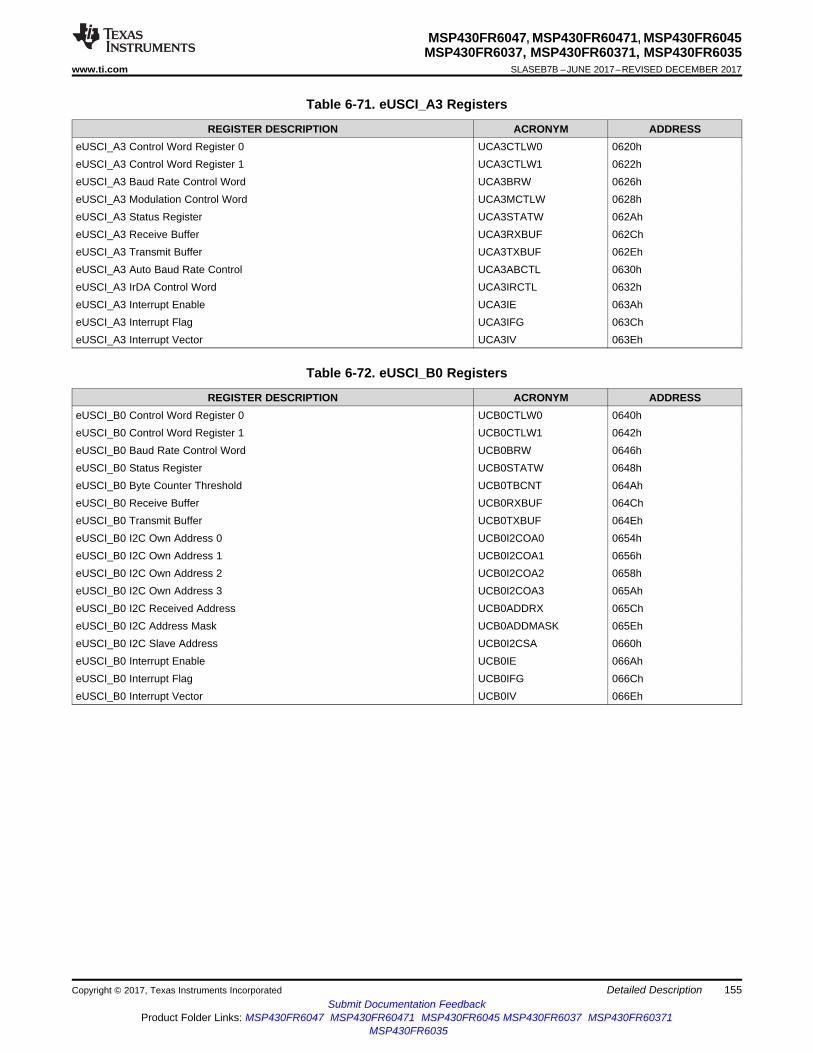
155
MSP430FR6047, MSP430FR60471, MSP430FR6045MSP430FR6037, MSP430FR60371, MSP430FR6035
www.ti.com SLASEB7B –JUNE 2017–REVISED DECEMBER 2017
Submit Documentation FeedbackProduct Folder Links: MSP430FR6047 MSP430FR60471 MSP430FR6045 MSP430FR6037 MSP430FR60371
MSP430FR6035
Detailed DescriptionCopyright © 2017, Texas Instruments Incorporated
Table 6-71. eUSCI_A3 Registers
REGISTER DESCRIPTION ACRONYM ADDRESSeUSCI_A3 Control Word Register 0 UCA3CTLW0 0620heUSCI_A3 Control Word Register 1 UCA3CTLW1 0622heUSCI_A3 Baud Rate Control Word UCA3BRW 0626heUSCI_A3 Modulation Control Word UCA3MCTLW 0628heUSCI_A3 Status Register UCA3STATW 062AheUSCI_A3 Receive Buffer UCA3RXBUF 062CheUSCI_A3 Transmit Buffer UCA3TXBUF 062EheUSCI_A3 Auto Baud Rate Control UCA3ABCTL 0630heUSCI_A3 IrDA Control Word UCA3IRCTL 0632heUSCI_A3 Interrupt Enable UCA3IE 063AheUSCI_A3 Interrupt Flag UCA3IFG 063CheUSCI_A3 Interrupt Vector UCA3IV 063Eh
Table 6-72. eUSCI_B0 Registers
REGISTER DESCRIPTION ACRONYM ADDRESSeUSCI_B0 Control Word Register 0 UCB0CTLW0 0640heUSCI_B0 Control Word Register 1 UCB0CTLW1 0642heUSCI_B0 Baud Rate Control Word UCB0BRW 0646heUSCI_B0 Status Register UCB0STATW 0648heUSCI_B0 Byte Counter Threshold UCB0TBCNT 064AheUSCI_B0 Receive Buffer UCB0RXBUF 064CheUSCI_B0 Transmit Buffer UCB0TXBUF 064EheUSCI_B0 I2C Own Address 0 UCB0I2COA0 0654heUSCI_B0 I2C Own Address 1 UCB0I2COA1 0656heUSCI_B0 I2C Own Address 2 UCB0I2COA2 0658heUSCI_B0 I2C Own Address 3 UCB0I2COA3 065AheUSCI_B0 I2C Received Address UCB0ADDRX 065CheUSCI_B0 I2C Address Mask UCB0ADDMASK 065EheUSCI_B0 I2C Slave Address UCB0I2CSA 0660heUSCI_B0 Interrupt Enable UCB0IE 066AheUSCI_B0 Interrupt Flag UCB0IFG 066CheUSCI_B0 Interrupt Vector UCB0IV 066Eh
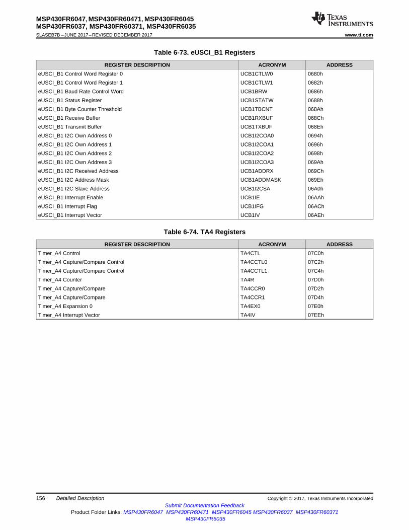
156
MSP430FR6047, MSP430FR60471, MSP430FR6045MSP430FR6037, MSP430FR60371, MSP430FR6035SLASEB7B –JUNE 2017–REVISED DECEMBER 2017 www.ti.com
Submit Documentation FeedbackProduct Folder Links: MSP430FR6047 MSP430FR60471 MSP430FR6045 MSP430FR6037 MSP430FR60371
MSP430FR6035
Detailed Description Copyright © 2017, Texas Instruments Incorporated
Table 6-73. eUSCI_B1 Registers
REGISTER DESCRIPTION ACRONYM ADDRESSeUSCI_B1 Control Word Register 0 UCB1CTLW0 0680heUSCI_B1 Control Word Register 1 UCB1CTLW1 0682heUSCI_B1 Baud Rate Control Word UCB1BRW 0686heUSCI_B1 Status Register UCB1STATW 0688heUSCI_B1 Byte Counter Threshold UCB1TBCNT 068AheUSCI_B1 Receive Buffer UCB1RXBUF 068CheUSCI_B1 Transmit Buffer UCB1TXBUF 068EheUSCI_B1 I2C Own Address 0 UCB1I2COA0 0694heUSCI_B1 I2C Own Address 1 UCB1I2COA1 0696heUSCI_B1 I2C Own Address 2 UCB1I2COA2 0698heUSCI_B1 I2C Own Address 3 UCB1I2COA3 069AheUSCI_B1 I2C Received Address UCB1ADDRX 069CheUSCI_B1 I2C Address Mask UCB1ADDMASK 069EheUSCI_B1 I2C Slave Address UCB1I2CSA 06A0heUSCI_B1 Interrupt Enable UCB1IE 06AAheUSCI_B1 Interrupt Flag UCB1IFG 06ACheUSCI_B1 Interrupt Vector UCB1IV 06AEh
Table 6-74. TA4 Registers
REGISTER DESCRIPTION ACRONYM ADDRESSTimer_A4 Control TA4CTL 07C0hTimer_A4 Capture/Compare Control TA4CCTL0 07C2hTimer_A4 Capture/Compare Control TA4CCTL1 07C4hTimer_A4 Counter TA4R 07D0hTimer_A4 Capture/Compare TA4CCR0 07D2hTimer_A4 Capture/Compare TA4CCR1 07D4hTimer_A4 Expansion 0 TA4EX0 07E0hTimer_A4 Interrupt Vector TA4IV 07EEh
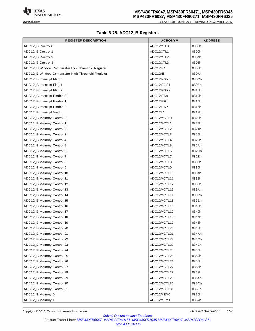
157
MSP430FR6047, MSP430FR60471, MSP430FR6045MSP430FR6037, MSP430FR60371, MSP430FR6035
www.ti.com SLASEB7B –JUNE 2017–REVISED DECEMBER 2017
Submit Documentation FeedbackProduct Folder Links: MSP430FR6047 MSP430FR60471 MSP430FR6045 MSP430FR6037 MSP430FR60371
MSP430FR6035
Detailed DescriptionCopyright © 2017, Texas Instruments Incorporated
Table 6-75. ADC12_B Registers
REGISTER DESCRIPTION ACRONYM ADDRESSADC12_B Control 0 ADC12CTL0 0800hADC12_B Control 1 ADC12CTL1 0802hADC12_B Control 2 ADC12CTL2 0804hADC12_B Control 3 ADC12CTL3 0806hADC12_B Window Comparator Low Threshold Register ADC12LO 0808hADC12_B Window Comparator High Threshold Register ADC12HI 080AhADC12_B Interrupt Flag 0 ADC12IFGR0 080ChADC12_B Interrupt Flag 1 ADC12IFGR1 080EhADC12_B Interrupt Flag 2 ADC12IFGR2 0810hADC12_B Interrupt Enable 0 ADC12IER0 0812hADC12_B Interrupt Enable 1 ADC12IER1 0814hADC12_B Interrupt Enable 2 ADC12IER2 0816hADC12_B Interrupt Vector ADC12IV 0818hADC12_B Memory Control 0 ADC12MCTL0 0820hADC12_B Memory Control 1 ADC12MCTL1 0822hADC12_B Memory Control 2 ADC12MCTL2 0824hADC12_B Memory Control 3 ADC12MCTL3 0826hADC12_B Memory Control 4 ADC12MCTL4 0828hADC12_B Memory Control 5 ADC12MCTL5 082AhADC12_B Memory Control 6 ADC12MCTL6 082ChADC12_B Memory Control 7 ADC12MCTL7 082EhADC12_B Memory Control 8 ADC12MCTL8 0830hADC12_B Memory Control 9 ADC12MCTL9 0832hADC12_B Memory Control 10 ADC12MCTL10 0834hADC12_B Memory Control 11 ADC12MCTL11 0836hADC12_B Memory Control 12 ADC12MCTL12 0838hADC12_B Memory Control 13 ADC12MCTL13 083AhADC12_B Memory Control 14 ADC12MCTL14 083ChADC12_B Memory Control 15 ADC12MCTL15 083EhADC12_B Memory Control 16 ADC12MCTL16 0840hADC12_B Memory Control 17 ADC12MCTL17 0842hADC12_B Memory Control 18 ADC12MCTL18 0844hADC12_B Memory Control 19 ADC12MCTL19 0846hADC12_B Memory Control 20 ADC12MCTL20 0848hADC12_B Memory Control 21 ADC12MCTL21 084AhADC12_B Memory Control 22 ADC12MCTL22 084ChADC12_B Memory Control 23 ADC12MCTL23 084EhADC12_B Memory Control 24 ADC12MCTL24 0850hADC12_B Memory Control 25 ADC12MCTL25 0852hADC12_B Memory Control 26 ADC12MCTL26 0854hADC12_B Memory Control 27 ADC12MCTL27 0856hADC12_B Memory Control 28 ADC12MCTL28 0858hADC12_B Memory Control 29 ADC12MCTL29 085AhADC12_B Memory Control 30 ADC12MCTL30 085ChADC12_B Memory Control 31 ADC12MCTL31 085EhADC12_B Memory 0 ADC12MEM0 0860hADC12_B Memory 1 ADC12MEM1 0862h
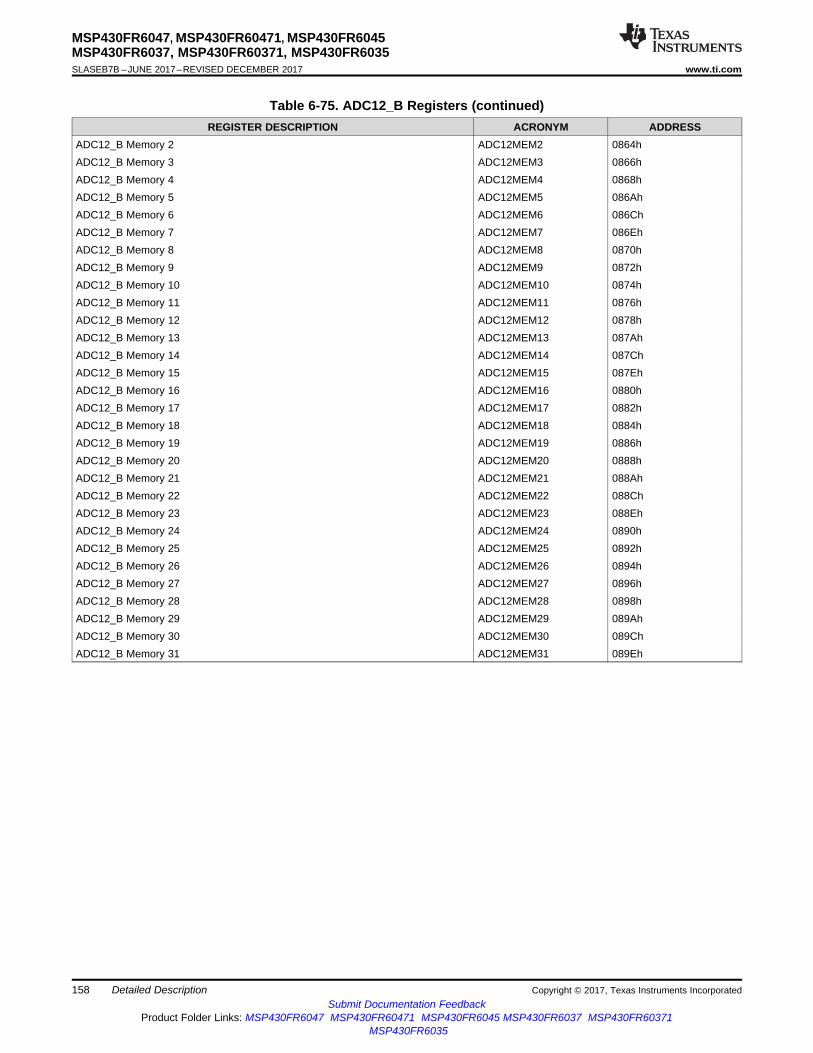
158
MSP430FR6047, MSP430FR60471, MSP430FR6045MSP430FR6037, MSP430FR60371, MSP430FR6035SLASEB7B –JUNE 2017–REVISED DECEMBER 2017 www.ti.com
Submit Documentation FeedbackProduct Folder Links: MSP430FR6047 MSP430FR60471 MSP430FR6045 MSP430FR6037 MSP430FR60371
MSP430FR6035
Detailed Description Copyright © 2017, Texas Instruments Incorporated
Table 6-75. ADC12_B Registers (continued)REGISTER DESCRIPTION ACRONYM ADDRESS
ADC12_B Memory 2 ADC12MEM2 0864hADC12_B Memory 3 ADC12MEM3 0866hADC12_B Memory 4 ADC12MEM4 0868hADC12_B Memory 5 ADC12MEM5 086AhADC12_B Memory 6 ADC12MEM6 086ChADC12_B Memory 7 ADC12MEM7 086EhADC12_B Memory 8 ADC12MEM8 0870hADC12_B Memory 9 ADC12MEM9 0872hADC12_B Memory 10 ADC12MEM10 0874hADC12_B Memory 11 ADC12MEM11 0876hADC12_B Memory 12 ADC12MEM12 0878hADC12_B Memory 13 ADC12MEM13 087AhADC12_B Memory 14 ADC12MEM14 087ChADC12_B Memory 15 ADC12MEM15 087EhADC12_B Memory 16 ADC12MEM16 0880hADC12_B Memory 17 ADC12MEM17 0882hADC12_B Memory 18 ADC12MEM18 0884hADC12_B Memory 19 ADC12MEM19 0886hADC12_B Memory 20 ADC12MEM20 0888hADC12_B Memory 21 ADC12MEM21 088AhADC12_B Memory 22 ADC12MEM22 088ChADC12_B Memory 23 ADC12MEM23 088EhADC12_B Memory 24 ADC12MEM24 0890hADC12_B Memory 25 ADC12MEM25 0892hADC12_B Memory 26 ADC12MEM26 0894hADC12_B Memory 27 ADC12MEM27 0896hADC12_B Memory 28 ADC12MEM28 0898hADC12_B Memory 29 ADC12MEM29 089AhADC12_B Memory 30 ADC12MEM30 089ChADC12_B Memory 31 ADC12MEM31 089Eh
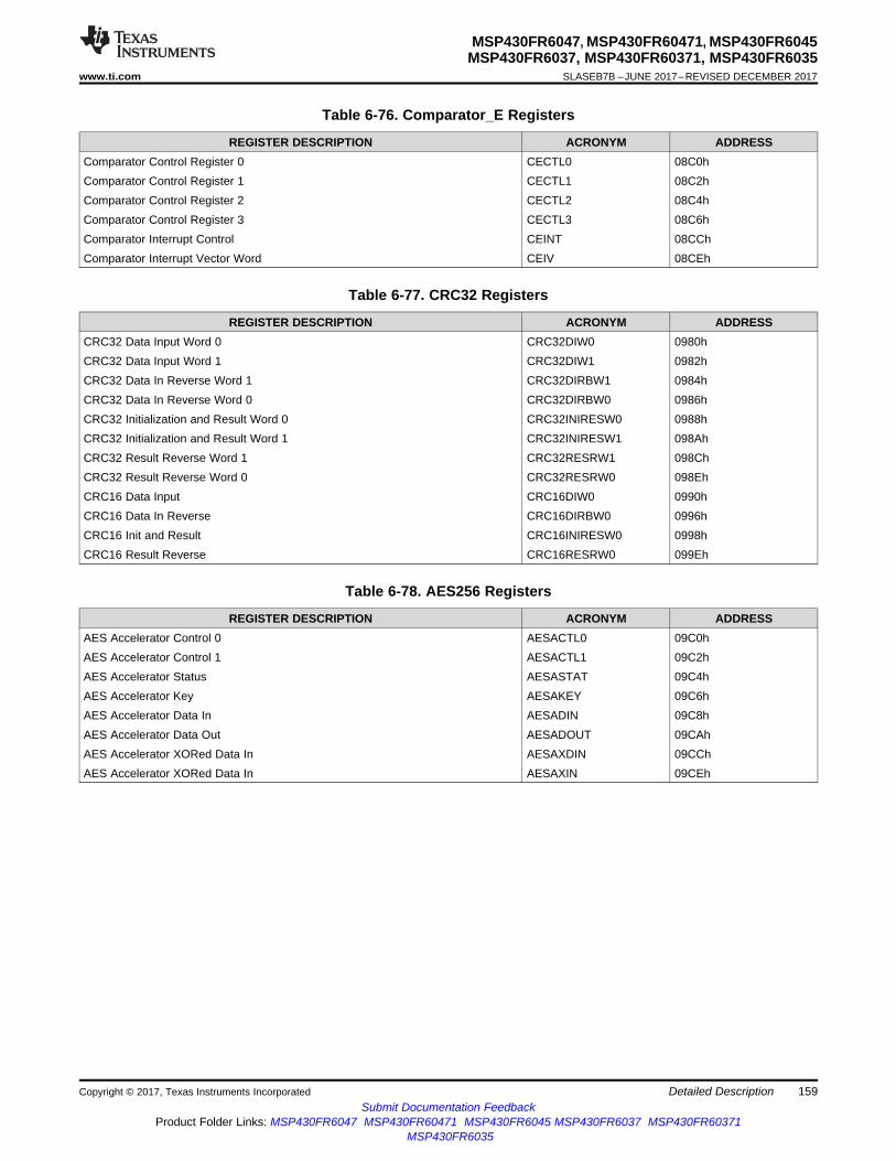
159
MSP430FR6047, MSP430FR60471, MSP430FR6045MSP430FR6037, MSP430FR60371, MSP430FR6035
www.ti.com SLASEB7B –JUNE 2017–REVISED DECEMBER 2017
Submit Documentation FeedbackProduct Folder Links: MSP430FR6047 MSP430FR60471 MSP430FR6045 MSP430FR6037 MSP430FR60371
MSP430FR6035
Detailed DescriptionCopyright © 2017, Texas Instruments Incorporated
Table 6-76. Comparator_E Registers
REGISTER DESCRIPTION ACRONYM ADDRESSComparator Control Register 0 CECTL0 08C0hComparator Control Register 1 CECTL1 08C2hComparator Control Register 2 CECTL2 08C4hComparator Control Register 3 CECTL3 08C6hComparator Interrupt Control CEINT 08CChComparator Interrupt Vector Word CEIV 08CEh
Table 6-77. CRC32 Registers
REGISTER DESCRIPTION ACRONYM ADDRESSCRC32 Data Input Word 0 CRC32DIW0 0980hCRC32 Data Input Word 1 CRC32DIW1 0982hCRC32 Data In Reverse Word 1 CRC32DIRBW1 0984hCRC32 Data In Reverse Word 0 CRC32DIRBW0 0986hCRC32 Initialization and Result Word 0 CRC32INIRESW0 0988hCRC32 Initialization and Result Word 1 CRC32INIRESW1 098AhCRC32 Result Reverse Word 1 CRC32RESRW1 098ChCRC32 Result Reverse Word 0 CRC32RESRW0 098EhCRC16 Data Input CRC16DIW0 0990hCRC16 Data In Reverse CRC16DIRBW0 0996hCRC16 Init and Result CRC16INIRESW0 0998hCRC16 Result Reverse CRC16RESRW0 099Eh
Table 6-78. AES256 Registers
REGISTER DESCRIPTION ACRONYM ADDRESSAES Accelerator Control 0 AESACTL0 09C0hAES Accelerator Control 1 AESACTL1 09C2hAES Accelerator Status AESASTAT 09C4hAES Accelerator Key AESAKEY 09C6hAES Accelerator Data In AESADIN 09C8hAES Accelerator Data Out AESADOUT 09CAhAES Accelerator XORed Data In AESAXDIN 09CChAES Accelerator XORed Data In AESAXIN 09CEh
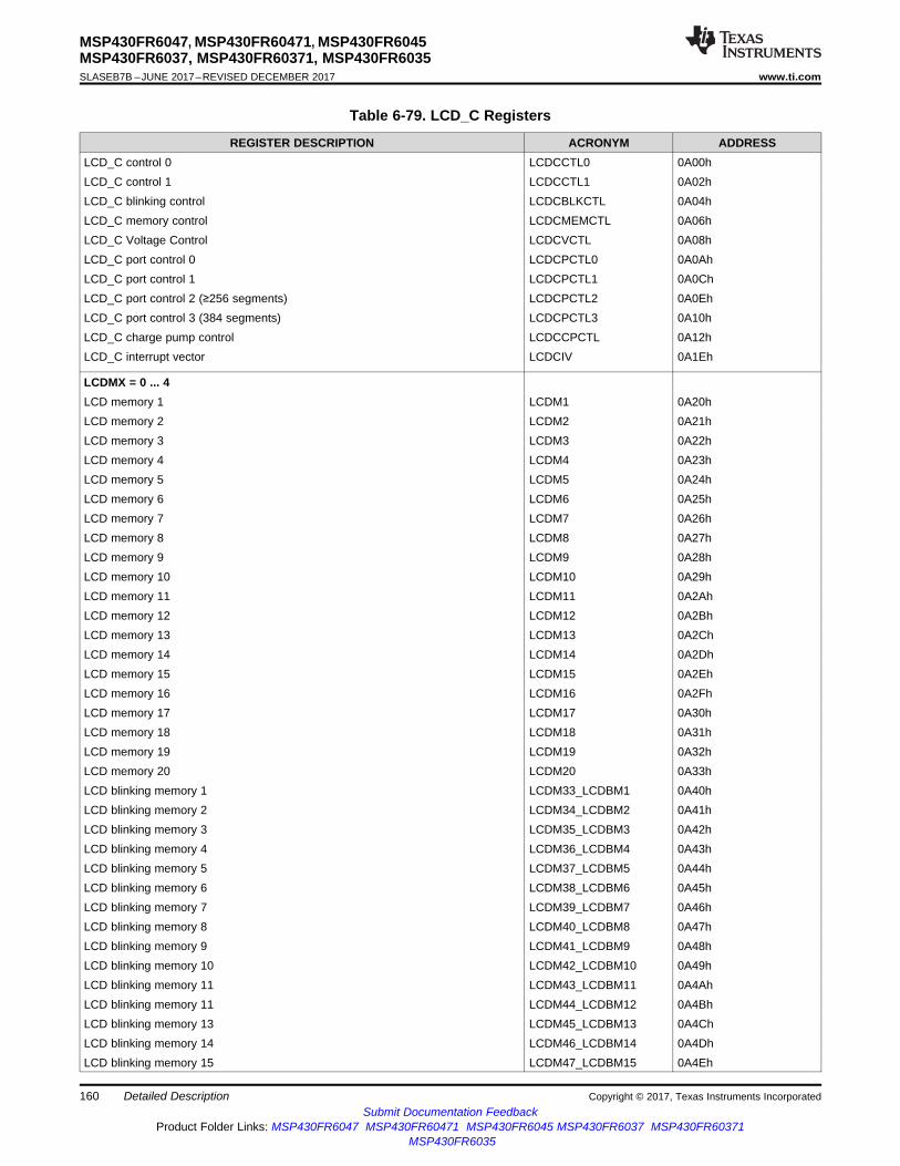
160
MSP430FR6047, MSP430FR60471, MSP430FR6045MSP430FR6037, MSP430FR60371, MSP430FR6035SLASEB7B –JUNE 2017–REVISED DECEMBER 2017 www.ti.com
Submit Documentation FeedbackProduct Folder Links: MSP430FR6047 MSP430FR60471 MSP430FR6045 MSP430FR6037 MSP430FR60371
MSP430FR6035
Detailed Description Copyright © 2017, Texas Instruments Incorporated
Table 6-79. LCD_C Registers
REGISTER DESCRIPTION ACRONYM ADDRESSLCD_C control 0 LCDCCTL0 0A00hLCD_C control 1 LCDCCTL1 0A02hLCD_C blinking control LCDCBLKCTL 0A04hLCD_C memory control LCDCMEMCTL 0A06hLCD_C Voltage Control LCDCVCTL 0A08hLCD_C port control 0 LCDCPCTL0 0A0AhLCD_C port control 1 LCDCPCTL1 0A0ChLCD_C port control 2 (≥256 segments) LCDCPCTL2 0A0EhLCD_C port control 3 (384 segments) LCDCPCTL3 0A10hLCD_C charge pump control LCDCCPCTL 0A12hLCD_C interrupt vector LCDCIV 0A1Eh
LCDMX = 0 ... 4LCD memory 1 LCDM1 0A20hLCD memory 2 LCDM2 0A21hLCD memory 3 LCDM3 0A22hLCD memory 4 LCDM4 0A23hLCD memory 5 LCDM5 0A24hLCD memory 6 LCDM6 0A25hLCD memory 7 LCDM7 0A26hLCD memory 8 LCDM8 0A27hLCD memory 9 LCDM9 0A28hLCD memory 10 LCDM10 0A29hLCD memory 11 LCDM11 0A2AhLCD memory 12 LCDM12 0A2BhLCD memory 13 LCDM13 0A2ChLCD memory 14 LCDM14 0A2DhLCD memory 15 LCDM15 0A2EhLCD memory 16 LCDM16 0A2FhLCD memory 17 LCDM17 0A30hLCD memory 18 LCDM18 0A31hLCD memory 19 LCDM19 0A32hLCD memory 20 LCDM20 0A33hLCD blinking memory 1 LCDM33_LCDBM1 0A40hLCD blinking memory 2 LCDM34_LCDBM2 0A41hLCD blinking memory 3 LCDM35_LCDBM3 0A42hLCD blinking memory 4 LCDM36_LCDBM4 0A43hLCD blinking memory 5 LCDM37_LCDBM5 0A44hLCD blinking memory 6 LCDM38_LCDBM6 0A45hLCD blinking memory 7 LCDM39_LCDBM7 0A46hLCD blinking memory 8 LCDM40_LCDBM8 0A47hLCD blinking memory 9 LCDM41_LCDBM9 0A48hLCD blinking memory 10 LCDM42_LCDBM10 0A49hLCD blinking memory 11 LCDM43_LCDBM11 0A4AhLCD blinking memory 11 LCDM44_LCDBM12 0A4BhLCD blinking memory 13 LCDM45_LCDBM13 0A4ChLCD blinking memory 14 LCDM46_LCDBM14 0A4DhLCD blinking memory 15 LCDM47_LCDBM15 0A4Eh
161
MSP430FR6047, MSP430FR60471, MSP430FR6045MSP430FR6037, MSP430FR60371, MSP430FR6035
www.ti.com SLASEB7B –JUNE 2017–REVISED DECEMBER 2017
Submit Documentation FeedbackProduct Folder Links: MSP430FR6047 MSP430FR60471 MSP430FR6045 MSP430FR6037 MSP430FR60371
MSP430FR6035
Detailed DescriptionCopyright © 2017, Texas Instruments Incorporated
Table 6-79. LCD_C Registers (continued)REGISTER DESCRIPTION ACRONYM ADDRESS
LCD blinking memory 16 LCDM48_LCDBM16 0A4FhLCD blinking memory 17 LCDM49_LCDBM17 0A50hLCD blinking memory 18 LCDM50_LCDBM18 0A51hLCD blinking memory 19 LCDM51_LCDBM19 0A52hLCD blinking memory 20 LCDM52_LCDBM20 0A53h
LCDMX = 5 ... 8LCD memory 1 LCDM1 0A20hLCD memory 2 LCDM2 0A21hLCD memory 3 LCDM3 0A22hLCD memory 4 LCDM4 0A23hLCD memory 5 LCDM5 0A24hLCD memory 6 LCDM6 0A25hLCD memory 7 LCDM7 0A26hLCD memory 8 LCDM8 0A27hLCD memory 9 LCDM9 0A28hLCD memory 10 LCDM10 0A29hLCD memory 11 LCDM11 0A2AhLCD memory 12 LCDM12 0A2BhLCD memory 13 LCDM13 0A2ChLCD memory 14 LCDM14 0A2DhLCD memory 15 LCDM15 0A2EhLCD memory 16 LCDM16 0A2FhLCD memory 17 LCDM17 0A30hLCD memory 18 LCDM18 0A31hLCD memory 19 LCDM19 0A32hLCD memory 20 LCDM20 0A33hLCD memory 21 LCDM21 0A34hLCD memory 22 LCDM22 0A35hLCD memory 23 LCDM23 0A36hLCD memory 24 LCDM24 0A37hLCD memory 25 LCDM25 0A38hLCD memory 26 LCDM26 0A39hLCD memory 27 LCDM27 0A3AhLCD memory 28 LCDM28 0A3BhLCD memory 29 LCDM29 0A3ChLCD memory 30 LCDM30 0A3DhLCD memory 31 LCDM31 0A3EhLCD memory 32 LCDM32 0A3FhLCD memory 33 LCDM33_LCDBM1 0A40hLCD memory 34 LCDM34_LCDBM2 0A41hLCD memory 35 LCDM35_LCDBM3 0A42hLCD memory 36 LCDM36_LCDBM4 0A43h

162
MSP430FR6047, MSP430FR60471, MSP430FR6045MSP430FR6037, MSP430FR60371, MSP430FR6035SLASEB7B –JUNE 2017–REVISED DECEMBER 2017 www.ti.com
Submit Documentation FeedbackProduct Folder Links: MSP430FR6047 MSP430FR60471 MSP430FR6045 MSP430FR6037 MSP430FR60371
MSP430FR6035
Detailed Description Copyright © 2017, Texas Instruments Incorporated
Table 6-80. LEA Registers
REGISTER DESCRIPTION ACRONYM ADDRESSLEA Capability Register LEACAP 0A80hConfiguration Register 0 LEACNF0 0A84hConfiguration Register 1 LEACNF1 0A88hConfiguration Register 2 LEACNF2 0A8ChMemory Bottom Register LEAMB 0A90hMemory Top Register LEAMT 0A94hCode Memory Access LEACMA 0A98hCode Memory Control LEACMCTL 0A9ChLEA Command Status LEACMDSTAT 0AA8hLEA Source 1 Status LEAS1STAT 0AAChLEA Source 0 Status LEAS0STAT 0AB0hLEA Result Status LEADSTSTAT 0AB4hPM Control Register LEAPMCTL 0AC0hPM Result Register LEAPMDST 0AC4hPM Source 1 Register LEAPMS1 0AC8hPM Source 0 Register LEAPMS0 0ACChPM Command Buffer LEAPMCB 0AD0hInterrupt Flag and Set LEAIFGSET 0AF0hInterrupt Enable LEAIE 0AF4hInterrupt Flag and Clear LEAIFG 0AF8hInterrupt Vector LEAIV 0AFCh

163
MSP430FR6047, MSP430FR60471, MSP430FR6045MSP430FR6037, MSP430FR60371, MSP430FR6035
www.ti.com SLASEB7B –JUNE 2017–REVISED DECEMBER 2017
Submit Documentation FeedbackProduct Folder Links: MSP430FR6047 MSP430FR60471 MSP430FR6045 MSP430FR6037 MSP430FR60371
MSP430FR6035
Detailed DescriptionCopyright © 2017, Texas Instruments Incorporated
Table 6-81. SAPH Registers
REGISTER DESCRIPTION ACRONYM ADDRESSInterrupt Index SAPHIIDX 0E00hMasked Interrupt Satus SAPHMIS 0E02hRaw Interrupt Status SAPHRIS 0E04hInterrupt Mask SAPHIMSC 0E06hInterrupt Clear SAPHICR 0E08hInterrupt Set SAPHISR 0E0AhModule-Descriptor Low Word SAPHDESCLO 0E0ChModule-Descriptor High Word SAPHDESCHI 0E0EhKey SAPHKEY 0E10hPhysical Interface Output Control #0 SAPHOCTL0 0E12hPhysical Interface Output Control #1 SAPHOCTL1 0E14hPhysical Interface Output Function Select SAPHOSEL 0E16hChannel 0 Pull UpTrim SAPHCH0PUT 0E20hChannel 0 Pull DownTrim SAPHCH0PDT 0E22hChannel 0 Termination Trim SAPHCH0TT 0E24hChannel 1 Pull UpTrim SAPHCH1PUT 0E26hChannel 1 Pull DownTrim SAPHCH1PDT 0E28hChannel 1 Termination Trim SAPHCH1TT 0E2AhMode Configuration Register SAPHMCNF 0E2ChTrim Access Control SAPHTACTL 0E2EhPhysical Interface Input Control #0 SAPHICTL0 0E30hBias Control SAPHBCTL 0E34hPPG Count SAPHPGC 0E40hPulse Generator Low Period SAPHPGLPER 0E42hPulse Generator High Period SAPHPGHPER 0E44hPPG Control SAPHPGCTL 0E46hPPG Software Trigger SAPHPPGTRIG 0E48hA-SEQ control 0 SAPHASCTL0 0E60hA-SEQ control 1 SAPHASCTL1 0E62hASQ Software Trigger SAPHASQTRIG 0E64hASQ ping output polarity SAPHAPOL 0E66hASQ ping pause level SAPHAPLEV 0E68hASQ ping pause impedance SAPHAPHIZ 0E6AhA-SEQ start to 1st ping SAPHATM_A 0E6EhASQ start to ADC arm SAPHATM_B 0E70hCount for the TIMEMARK C Event SAPHATM_C 0E72hASQ start to ADC trig SAPHATM_D 0E74hASQ start to restart SAPHATM_E 0E76hASQ start to time-out SAPHATM_F 0E78hTime Base Control SAPHTBCTL 0E7AhAcquisition Timer Low Part SAPHATIMLO 0E7ChAcquisition Timer High Part SAPHATIMHI 0E7Eh

164
MSP430FR6047, MSP430FR60471, MSP430FR6045MSP430FR6037, MSP430FR60371, MSP430FR6035SLASEB7B –JUNE 2017–REVISED DECEMBER 2017 www.ti.com
Submit Documentation FeedbackProduct Folder Links: MSP430FR6047 MSP430FR60471 MSP430FR6045 MSP430FR6037 MSP430FR60371
MSP430FR6035
Detailed Description Copyright © 2017, Texas Instruments Incorporated
(1) Not available in MSP430FR6037, MSP430FR6035, and MSP430FR60371
Table 6-82. SDHS Registers (1)
REGISTER DESCRIPTION ACRONYM ADDRESSInterrupt Index Register SDHSIIDX 0E80hMasked Interrupt Status and Clear Register SDHSMIS 0E82hRaw Interrupt Status SDHSRIS 0E84hInterrupt Mask Register SDHSIMSC 0E86hInterrupt Clear SDHSICR 0E88hInterrupt Set Register SDHSISR 0E8AhSDHS Descriptor Register L SDHSDESCLO 0E8ChSDHS Descriptor Register H SDHSDESCHI 0E8EhSDHS Control Register 0 SDHSCTL0 0E90hSDHS Control Register 1 SDHSCTL1 0E92hSDHS Control Register 2 SDHSCTL2 0E94hSDHS Control Register 3 SDHSCTL3 0E96hSDHS Control Register 4 SDHSCTL4 0E98hSDHS Control Register 5 SDHSCTL5 0E9AhSDHS Control Register 6 SDHSCTL6 0E9ChSDHS Control Register 7 SDHSCTL7 0E9EhSDHS Data Converstion Register SDHSDT 0EA2hSDHS Window Comparator High Threshold Register SDHSWINHITH 0EA4hSDHS Window Comparator Low Threshold Register SDHSWINLOTH 0EA6hDTC destination address SDHSDTCDA 0EA8h
(1) Not available in MSP430FR6037, MSP430FR6035, and MSP430FR60371
Table 6-83. UUPS Registers (1)
REGISTER DESCRIPTION ACRONYM ADDRESSInterrupt Index Register UUPSIIDX 0EC0hMasked Interrupt Status UUPSMIS 0EC2hRaw Interrupt Status UUPSRIS 0EC4hInterrupt Mask Register UUPSIMSC 0EC6hInterrupt Clear UUPSICR 0EC8hInterrupt Flag Set UUPSISR 0ECAhUUPS Descriptor Register L UUPSDESCLO 0ECChUUPS Descriptor Register H UUPSDESCHI 0ECEhUUPS Control UUPSCTL 0ED0h
165
MSP430FR6047, MSP430FR60471, MSP430FR6045MSP430FR6037, MSP430FR60371, MSP430FR6035
www.ti.com SLASEB7B –JUNE 2017–REVISED DECEMBER 2017
Submit Documentation FeedbackProduct Folder Links: MSP430FR6047 MSP430FR60471 MSP430FR6045 MSP430FR6037 MSP430FR60371
MSP430FR6035
Detailed DescriptionCopyright © 2017, Texas Instruments Incorporated
(1) Not available in MSP430FR6037, MSP430FR6035, and MSP430FR60371
Table 6-84. HSPLL Registers (1)
REGISTER DESCRIPTION ACRONYM ADDRESSInterrupt Index Register HSPLLIIDX 0EE0hMasked Interrupt Status HSPLLMIS 0EE2hRaw Interrupt Status HSPLLRIS 0EE4hInterrupt Mask Register HSPLLIMSC 0EE6hInterrupt Flag Clear HSPLLICR 0EE8hInterrupt Flag Set HSPLLISR 0EEAhHSPLL Descriptor Register L HSPLLDESCLO 0EEChHSPLL Descriptor Register H HSPLLDESCHI 0EEEhHSPLL Control Register HSPLLCTL 0EF0hUSSXT Control Register HSPLLUSSXTLCTL 0EF2h
Table 6-85. MTIF Registers
REGISTER DESCRIPTION ACRONYM ADDRESSPulse Generator Configuration MTIFPGCNF 0F00hPulse Generator Value MTIFPGKVAL 0F02hPulse Generator Control MTIFPGCTL 0F04hPulse Generator Status MTIFPGSR 0F06hPulse Counter Configuration MTIFPCCNF 0F08hPulse Counter Value MTIFPCR 0F0AhPulse Counter Control MTIFPCCTL 0F0ChPulse Counter Status MTIFPCSR 0F0EhMeasurement Test Port Control MTIFTPCTL 0F10h
166
MSP430FR6047, MSP430FR60471, MSP430FR6045MSP430FR6037, MSP430FR60371, MSP430FR6035SLASEB7B –JUNE 2017–REVISED DECEMBER 2017 www.ti.com
Submit Documentation FeedbackProduct Folder Links: MSP430FR6047 MSP430FR60471 MSP430FR6045 MSP430FR6037 MSP430FR60371
MSP430FR6035
Detailed Description Copyright © 2017, Texas Instruments Incorporated
6.17 Identification
6.17.1 Revision IdentificationThe device revision information is shown as part of the top-side marking on the device package. Thedevice-specific errata sheet describes these markings. For links to the errata sheets for the devices in thisdata sheet, see Section 8.4.
The hardware revision is also stored in the Device Descriptor structure in the Info Block section. Fordetails on this value, see the "Hardware Revision" entries in the Device Descriptor structure (seeSection 6.15).
6.17.2 Device IdentificationThe device type can be identified from the top-side marking on the device package. The device-specificerrata sheet describes these markings. For links to the errata sheets for the devices in this data sheet, seeSection 8.4.
A device identification value is also stored in the Device Descriptor structure in the Info Block section. Fordetails on this value, see the "Device ID" entries in the Device Descriptor structure.
6.17.3 JTAG IdentificationProgramming through the JTAG interface, including reading and identifying the JTAG ID, is described inMSP430 Programming With the JTAG Interface.

USS module power supply decoupling
1 nF22 Fµ
PVCC
PVSS
+
22 W
Digital PowerSupply Decoupling
100 nF1 Fµ
Analog PowerSupply Decoupling
DVCC
DVSS
AVCC
AVSS
+
+
100 nF1 Fµ
167
MSP430FR6047, MSP430FR60471, MSP430FR6045MSP430FR6037, MSP430FR60371, MSP430FR6035
www.ti.com SLASEB7B –JUNE 2017–REVISED DECEMBER 2017
Submit Documentation FeedbackProduct Folder Links: MSP430FR6047 MSP430FR60471 MSP430FR6045 MSP430FR6037 MSP430FR60371
MSP430FR6035
Applications, Implementation, and LayoutCopyright © 2017, Texas Instruments Incorporated
7 Applications, Implementation, and Layout
NOTEInformation in the following Applications section is not part of the TI component specification,and TI does not warrant its accuracy or completeness. TI's customers are responsible fordetermining suitability of components for their purposes. Customers should validate and testtheir design implementation to confirm system functionality.
7.1 Device Connection and Layout FundamentalsThis section describes the recommended guidelines when designing with the MSP MCU. These guidelinesare to make sure that the device has proper connections for powering, programming, debugging, andoptimum analog performance.
7.1.1 Power Supply Decoupling and Bulk CapacitorsTI recommends connecting a combination of a 1-µF plus a 100-nF low-ESR ceramic decoupling capacitorto each AVCC and DVCC pin (see Figure 7-1). Higher-value capacitors may be used but can affect supplyrail ramp-up time. Decoupling capacitors must be placed as close as possible to the pins that theydecouple (within a few millimeters). Additionally, TI recommends separated grounds with a single-pointconnection for better noise isolation from digital to analog circuits on the board and to achieve high analogaccuracy.
Figure 7-1. Power Supply Decoupling
For PVCC and PVSS, TI recommends connecting a combination of a 1-µF plus a 22-µF low-ESR ceramicdecoupling capacitor between the PVCC and PVSS pins and a serial 22-Ω resistor to filter low-frequencynoise on the supply line (see Figure 7-2).
Figure 7-2. Power Supply Decoupling for PVCC and PVSS
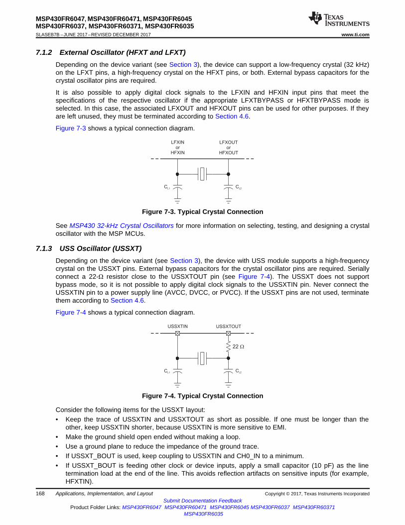
CL1
CL2
USSXTIN USSXTOUT
22 W
CL1
CL2
LFXIN
or
HFXIN
LFXOUT
or
HFXOUT
168
MSP430FR6047, MSP430FR60471, MSP430FR6045MSP430FR6037, MSP430FR60371, MSP430FR6035SLASEB7B –JUNE 2017–REVISED DECEMBER 2017 www.ti.com
Submit Documentation FeedbackProduct Folder Links: MSP430FR6047 MSP430FR60471 MSP430FR6045 MSP430FR6037 MSP430FR60371
MSP430FR6035
Applications, Implementation, and Layout Copyright © 2017, Texas Instruments Incorporated
7.1.2 External Oscillator (HFXT and LFXT)Depending on the device variant (see Section 3), the device can support a low-frequency crystal (32 kHz)on the LFXT pins, a high-frequency crystal on the HFXT pins, or both. External bypass capacitors for thecrystal oscillator pins are required.
It is also possible to apply digital clock signals to the LFXIN and HFXIN input pins that meet thespecifications of the respective oscillator if the appropriate LFXTBYPASS or HFXTBYPASS mode isselected. In this case, the associated LFXOUT and HFXOUT pins can be used for other purposes. If theyare left unused, they must be terminated according to Section 4.6.
Figure 7-3 shows a typical connection diagram.
Figure 7-3. Typical Crystal Connection
See MSP430 32-kHz Crystal Oscillators for more information on selecting, testing, and designing a crystaloscillator with the MSP MCUs.
7.1.3 USS Oscillator (USSXT)Depending on the device variant (see Section 3), the device with USS module supports a high-frequencycrystal on the USSXT pins. External bypass capacitors for the crystal oscillator pins are required. Seriallyconnect a 22-Ω resistor close to the USSXTOUT pin (see Figure 7-4). The USSXT does not supportbypass mode, so it is not possible to apply digital clock signals to the USSXTIN pin. Never connect theUSSXTIN pin to a power supply line (AVCC, DVCC, or PVCC). If the USSXT pins are not used, terminatethem according to Section 4.6.
Figure 7-4 shows a typical connection diagram.
Figure 7-4. Typical Crystal Connection
Consider the following items for the USSXT layout:• Keep the trace of USSXTIN and USSXTOUT as short as possible. If one must be longer than the
other, keep USSXTIN shorter, because USSXTIN is more sensitive to EMI.• Make the ground shield open ended without making a loop.• Use a ground plane to reduce the impedance of the ground trace.• If USSXT_BOUT is used, keep coupling to USSXTIN and CH0_IN to a minimum.• If USSXT_BOUT is feeding other clock or device inputs, apply a small capacitor (10 pF) as the line
termination load at the end of the line. This avoids reflection artifacts on sensitive inputs (for example,HFXTIN).
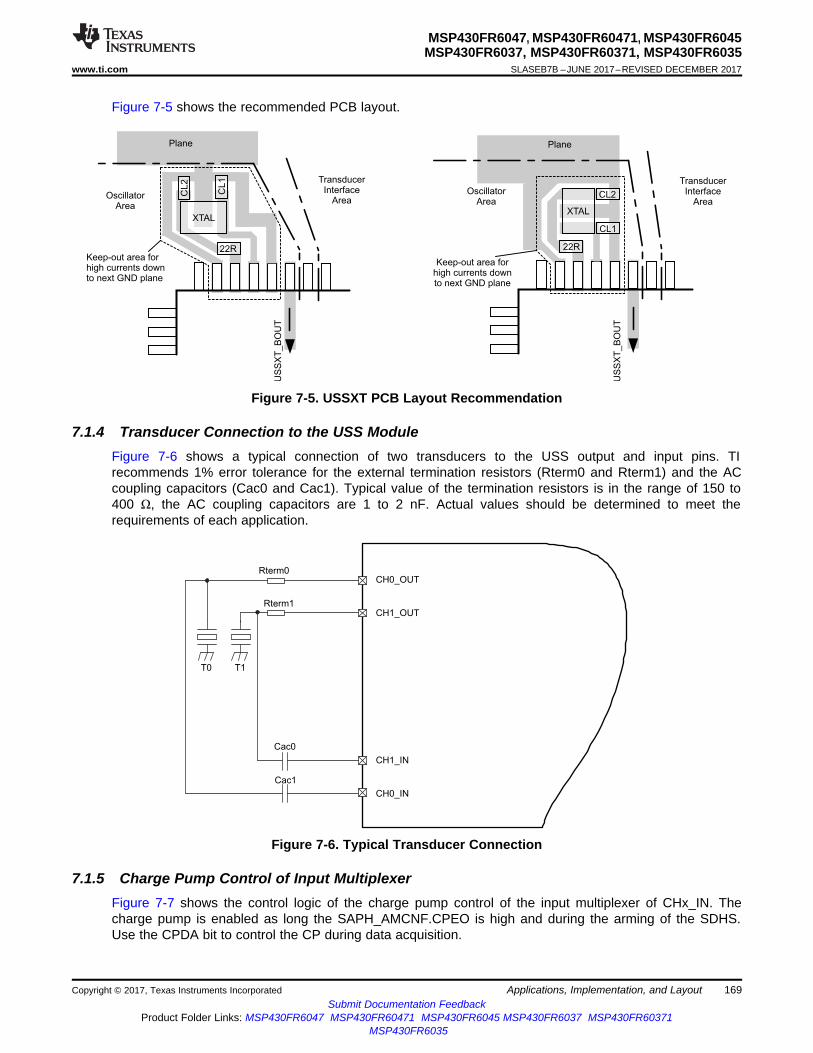
CH0_OUT
CH1_OUT
CH1_IN
CH0_IN
Rterm0
Rterm1
Cac0
T1T0
Cac1
XTAL
Plane
US
SX
T_B
OU
T
OscillatorArea
TransducerInterface
Area
Keep-out area forhigh currents downto next GND plane
22R
CL2
CL1
XTAL
Plane
US
SX
T_B
OU
T
OscillatorArea
TransducerInterface
Area
Keep-out area forhigh currents downto next GND plane
CL1
CL2
22R
169
MSP430FR6047, MSP430FR60471, MSP430FR6045MSP430FR6037, MSP430FR60371, MSP430FR6035
www.ti.com SLASEB7B –JUNE 2017–REVISED DECEMBER 2017
Submit Documentation FeedbackProduct Folder Links: MSP430FR6047 MSP430FR60471 MSP430FR6045 MSP430FR6037 MSP430FR60371
MSP430FR6035
Applications, Implementation, and LayoutCopyright © 2017, Texas Instruments Incorporated
Figure 7-5 shows the recommended PCB layout.
Figure 7-5. USSXT PCB Layout Recommendation
7.1.4 Transducer Connection to the USS ModuleFigure 7-6 shows a typical connection of two transducers to the USS output and input pins. TIrecommends 1% error tolerance for the external termination resistors (Rterm0 and Rterm1) and the ACcoupling capacitors (Cac0 and Cac1). Typical value of the termination resistors is in the range of 150 to400 Ω, the AC coupling capacitors are 1 to 2 nF. Actual values should be determined to meet therequirements of each application.
Figure 7-6. Typical Transducer Connection
7.1.5 Charge Pump Control of Input MultiplexerFigure 7-7 shows the control logic of the charge pump control of the input multiplexer of CHx_IN. Thecharge pump is enabled as long the SAPH_AMCNF.CPEO is high and during the arming of the SDHS.Use the CPDA bit to control the CP during data acquisition.

SDHS.acquisition
SAPH_AMCNF.CPEO
ASQ.acquisition
ASQ.adc_arming
SDHS.adc_arming
SAPH_ABCTL.CPDA
Chargepumpenable
PGA
MU
X
CPen
CH0_IN
CH1_INT SDHSo
170
MSP430FR6047, MSP430FR60471, MSP430FR6045MSP430FR6037, MSP430FR60371, MSP430FR6035SLASEB7B –JUNE 2017–REVISED DECEMBER 2017 www.ti.com
Submit Documentation FeedbackProduct Folder Links: MSP430FR6047 MSP430FR60471 MSP430FR6045 MSP430FR6037 MSP430FR60371
MSP430FR6035
Applications, Implementation, and Layout Copyright © 2017, Texas Instruments Incorporated
Figure 7-7. Control Of Input Multiplexer
7.1.6 JTAGWith the proper connections, the debugger and a hardware JTAG interface (such as the MSP-FET orMSP-FET430UIF) can be used to program and debug code on the target board. In addition, theconnections also support the MSP-GANG production programmers, thus providing an easy way toprogram prototype boards, if desired. Figure 7-8 shows the connections between the 14-pin JTAGconnector and the target device required to support in-system programming and debugging for 4-wireJTAG communication. Figure 7-9 shows the connections for 2-wire JTAG mode (Spy-Bi-Wire).
The connections for the MSP-FET and MSP-FET430UIF interface modules and the MSP-GANG areidentical. Both can supply VCC to the target board (through pin 2). In addition, the MSP-FET and MSP-FET430UIF interface modules and MSP-GANG have a VCC sense feature that, if used, requires analternate connection (pin 4 instead of pin 2). The VCC sense feature senses the local VCC present on thetarget board (that is, a battery or other local power supply) and adjusts the output signals accordingly.Figure 7-8 and Figure 7-9 show a jumper block that supports both scenarios of supplying VCC to the targetboard. If this flexibility is not required, the desired VCC connections may be hard-wired to eliminate thejumper block. Pins 2 and 4 must not be connected at the same time.
For additional design information regarding the JTAG interface, see the MSP430 Hardware Tools User’sGuide.
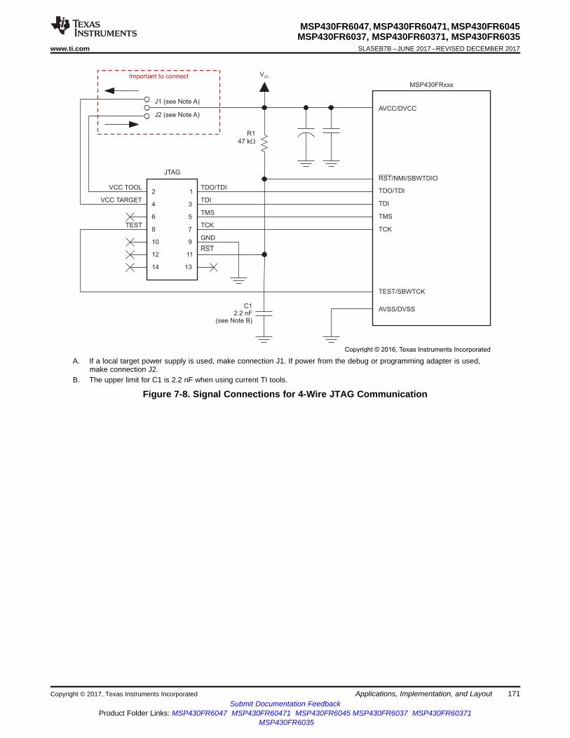
1
3
5
7
9
11
13
2
4
6
8
10
12
14
TDO/TDI
TDI
TMS
TCK
GND
TEST
JTAG
VCC TOOL
VCC TARGET
J1 (see Note A)
J2 (see Note A)
VCC
R1
47 kW
AV /DVCCCC
RST/NMI/SBWTDIO
TDO/TDI
TDI
TMS
TCK
TEST/SBWTCK
AV /DVSS SS
MSP430FRxxx
C12.2 nF
(see Note B)
RST
Important to connect
Copyright © 2016, Texas Instruments Incorporated
171
MSP430FR6047, MSP430FR60471, MSP430FR6045MSP430FR6037, MSP430FR60371, MSP430FR6035
www.ti.com SLASEB7B –JUNE 2017–REVISED DECEMBER 2017
Submit Documentation FeedbackProduct Folder Links: MSP430FR6047 MSP430FR60471 MSP430FR6045 MSP430FR6037 MSP430FR60371
MSP430FR6035
Applications, Implementation, and LayoutCopyright © 2017, Texas Instruments Incorporated
A. If a local target power supply is used, make connection J1. If power from the debug or programming adapter is used,make connection J2.
B. The upper limit for C1 is 2.2 nF when using current TI tools.
Figure 7-8. Signal Connections for 4-Wire JTAG Communication

1
3
5
7
9
11
13
2
4
6
8
10
12
14
TEST/SBWTCK
MSP430FRxxx
RST/NMI/SBWTDIOTDO/TDI
TCK
GND
JTAG
R147 kΩ
See Note B
VCC TOOL
VCC TARGET
C12.2 nF
See Note B
J1 (see Note A)
J2 (see Note A)
Important to connect
AV /DVCCCC
AV /DVSS SS
VCC
Copyright © 2016, Texas Instruments Incorporated
172
MSP430FR6047, MSP430FR60471, MSP430FR6045MSP430FR6037, MSP430FR60371, MSP430FR6035SLASEB7B –JUNE 2017–REVISED DECEMBER 2017 www.ti.com
Submit Documentation FeedbackProduct Folder Links: MSP430FR6047 MSP430FR60471 MSP430FR6045 MSP430FR6037 MSP430FR60371
MSP430FR6035
Applications, Implementation, and Layout Copyright © 2017, Texas Instruments Incorporated
A. Make connection J1 if a local target power supply is used, or make connection J2 if the target is powered from thedebug or programming adapter.
B. The device RST/NMI/SBWTDIO pin is used in 2-wire mode for bidirectional communication with the device duringJTAG access, and any capacitance that is attached to this signal may affect the ability to establish a connection withthe device. The upper limit for C1 is 2.2 nF when using current TI tools.
Figure 7-9. Signal Connections for 2-Wire JTAG Communication (Spy-Bi-Wire)
7.1.7 ResetThe reset pin can be configured as a reset function (default) or as an NMI function in the SFRRPCRregister.
In reset mode, the RST/NMI pin is active low, and a pulse applied to this pin that meets the reset timingspecifications generates a BOR-type device reset.
Setting SYSNMI causes the RST/NMI pin to be configured as an external NMI source. The external NMI isedge sensitive, and its edge is selectable by SYSNMIIES. Setting the NMIIE enables the interrupt of theexternal NMI. When an external NMI event occurs, the NMIIFG is set.
The RST/NMI pin can have either a pullup or pulldown that is enabled or not. SYSRSTUP selects eitherpullup or pulldown, and SYSRSTRE causes the pullup (default) or pulldown to be enabled (default) or not.If the RST/NMI pin is unused, it is required either to select and enable the internal pullup or to connect anexternal 47-kΩ pullup resistor to the RST/NMI pin with a 2.2-nF pulldown capacitor. The pulldowncapacitor should not exceed 2.2 nF when using devices with Spy-Bi-Wire interface in Spy-Bi-Wire mode orin 4-wire JTAG mode with TI tools like FET interfaces or GANG programmers.
See the MSP430FR58xx, MSP430FR59xx, and MSP430FR6xx Family User's Guide for more informationon the referenced control registers and bits.
7.1.8 Unused PinsFor details on the connection of unused pins, see Section 4.6.
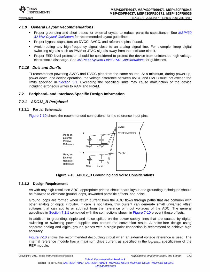
Using an
External
Positive
Reference
Using an
External
Negative
Reference
VEREF-
VREF+/VEREF+
+
+
4.7 µF10 Fµ
4.7 µF10 Fµ
AVSS
173
MSP430FR6047, MSP430FR60471, MSP430FR6045MSP430FR6037, MSP430FR60371, MSP430FR6035
www.ti.com SLASEB7B –JUNE 2017–REVISED DECEMBER 2017
Submit Documentation FeedbackProduct Folder Links: MSP430FR6047 MSP430FR60471 MSP430FR6045 MSP430FR6037 MSP430FR60371
MSP430FR6035
Applications, Implementation, and LayoutCopyright © 2017, Texas Instruments Incorporated
7.1.9 General Layout Recommendations• Proper grounding and short traces for external crystal to reduce parasitic capacitance. See MSP430
32-kHz Crystal Oscillators for recommended layout guidelines.• Proper bypass capacitors on DVCC, AVCC, and reference pins if used.• Avoid routing any high-frequency signal close to an analog signal line. For example, keep digital
switching signals such as PWM or JTAG signals away from the oscillator circuit.• Proper ESD level protection should be considered to protect the device from unintended high-voltage
electrostatic discharge. See MSP430 System-Level ESD Considerations for guidelines.
7.1.10 Do's and Don'tsTI recommends powering AVCC and DVCC pins from the same source. At a minimum, during power up,power down, and device operation, the voltage difference between AVCC and DVCC must not exceed thelimits specified in Section 5.1. Exceeding the specified limits may cause malfunction of the deviceincluding erroneous writes to RAM and FRAM.
7.2 Peripheral- and Interface-Specific Design Information
7.2.1 ADC12_B Peripheral
7.2.1.1 Partial Schematic
Figure 7-10 shows the recommended connections for the reference input pins.
Figure 7-10. ADC12_B Grounding and Noise Considerations
7.2.1.2 Design Requirements
As with any high-resolution ADC, appropriate printed-circuit-board layout and grounding techniques shouldbe followed to eliminate ground loops, unwanted parasitic effects, and noise.
Ground loops are formed when return current from the ADC flows through paths that are common withother analog or digital circuitry. If care is not taken, this current can generate small unwanted offsetvoltages that can add to or subtract from the reference or input voltages of the ADC. The generalguidelines in Section 7.1.1 combined with the connections shown in Figure 7-10 prevent these offsets.
In addition to grounding, ripple and noise spikes on the power-supply lines that are caused by digitalswitching or switching power supplies can corrupt the conversion result. A noise-free design usingseparate analog and digital ground planes with a single-point connection is recommend to achieve highaccuracy.
Figure 7-10 shows the recommended decoupling circuit when an external voltage reference is used. Theinternal reference module has a maximum drive current as specified in the IO(VREF+) specification of theREF module.
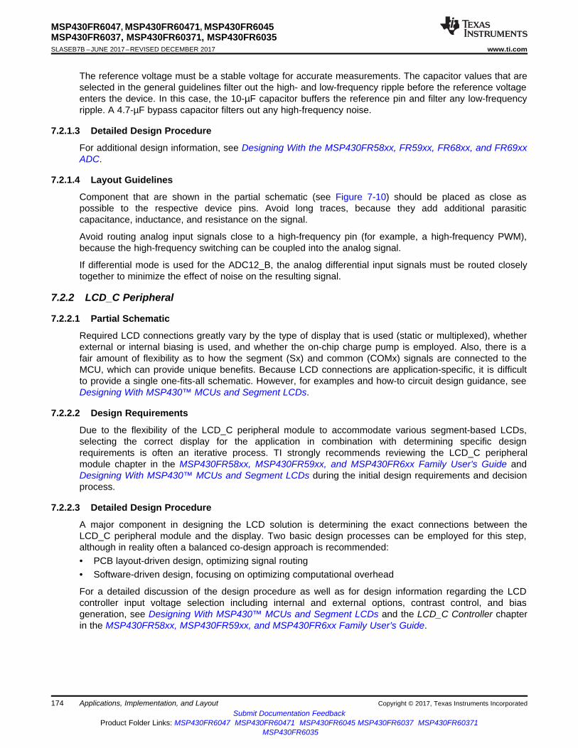
174
MSP430FR6047, MSP430FR60471, MSP430FR6045MSP430FR6037, MSP430FR60371, MSP430FR6035SLASEB7B –JUNE 2017–REVISED DECEMBER 2017 www.ti.com
Submit Documentation FeedbackProduct Folder Links: MSP430FR6047 MSP430FR60471 MSP430FR6045 MSP430FR6037 MSP430FR60371
MSP430FR6035
Applications, Implementation, and Layout Copyright © 2017, Texas Instruments Incorporated
The reference voltage must be a stable voltage for accurate measurements. The capacitor values that areselected in the general guidelines filter out the high- and low-frequency ripple before the reference voltageenters the device. In this case, the 10-µF capacitor buffers the reference pin and filter any low-frequencyripple. A 4.7-µF bypass capacitor filters out any high-frequency noise.
7.2.1.3 Detailed Design Procedure
For additional design information, see Designing With the MSP430FR58xx, FR59xx, FR68xx, and FR69xxADC.
7.2.1.4 Layout Guidelines
Component that are shown in the partial schematic (see Figure 7-10) should be placed as close aspossible to the respective device pins. Avoid long traces, because they add additional parasiticcapacitance, inductance, and resistance on the signal.
Avoid routing analog input signals close to a high-frequency pin (for example, a high-frequency PWM),because the high-frequency switching can be coupled into the analog signal.
If differential mode is used for the ADC12_B, the analog differential input signals must be routed closelytogether to minimize the effect of noise on the resulting signal.
7.2.2 LCD_C Peripheral
7.2.2.1 Partial Schematic
Required LCD connections greatly vary by the type of display that is used (static or multiplexed), whetherexternal or internal biasing is used, and whether the on-chip charge pump is employed. Also, there is afair amount of flexibility as to how the segment (Sx) and common (COMx) signals are connected to theMCU, which can provide unique benefits. Because LCD connections are application-specific, it is difficultto provide a single one-fits-all schematic. However, for examples and how-to circuit design guidance, seeDesigning With MSP430™ MCUs and Segment LCDs.
7.2.2.2 Design Requirements
Due to the flexibility of the LCD_C peripheral module to accommodate various segment-based LCDs,selecting the correct display for the application in combination with determining specific designrequirements is often an iterative process. TI strongly recommends reviewing the LCD_C peripheralmodule chapter in the MSP430FR58xx, MSP430FR59xx, and MSP430FR6xx Family User's Guide andDesigning With MSP430™ MCUs and Segment LCDs during the initial design requirements and decisionprocess.
7.2.2.3 Detailed Design Procedure
A major component in designing the LCD solution is determining the exact connections between theLCD_C peripheral module and the display. Two basic design processes can be employed for this step,although in reality often a balanced co-design approach is recommended:• PCB layout-driven design, optimizing signal routing• Software-driven design, focusing on optimizing computational overhead
For a detailed discussion of the design procedure as well as for design information regarding the LCDcontroller input voltage selection including internal and external options, contrast control, and biasgeneration, see Designing With MSP430™ MCUs and Segment LCDs and the LCD_C Controller chapterin the MSP430FR58xx, MSP430FR59xx, and MSP430FR6xx Family User's Guide.
175
MSP430FR6047, MSP430FR60471, MSP430FR6045MSP430FR6037, MSP430FR60371, MSP430FR6035
www.ti.com SLASEB7B –JUNE 2017–REVISED DECEMBER 2017
Submit Documentation FeedbackProduct Folder Links: MSP430FR6047 MSP430FR60471 MSP430FR6045 MSP430FR6037 MSP430FR60371
MSP430FR6035
Applications, Implementation, and LayoutCopyright © 2017, Texas Instruments Incorporated
7.2.2.4 Layout Guidelines
LCD segment (Sx) and common (COMx) signal traces are continuously switching while the LCD isenabled and should, therefore, be kept away from sensitive analog signals such as ADC inputs to preventany noise coupling. TI recommends keeping the LCD signal traces on one side of the PCB groupedtogether in a bus-like fashion. A ground plane beneath the LCD traces and guard traces alongside theLCD traces can provide shielding.
If the internal charge pump of the LCD module is used, place the externally provided capacitor on theLCDCAP pin as close as possible to the MCU. Connect the capacitor to the device using a short anddirect trace and also have a solid connection to the ground plane that supplies the VSS pins of the MCU.
For an example layouts and a more in-depth discussion, see Designing With MSP430™ MCUs andSegment LCDs.

176
MSP430FR6047, MSP430FR60471, MSP430FR6045MSP430FR6037, MSP430FR60371, MSP430FR6035SLASEB7B –JUNE 2017–REVISED DECEMBER 2017 www.ti.com
Submit Documentation FeedbackProduct Folder Links: MSP430FR6047 MSP430FR60471 MSP430FR6045 MSP430FR6037 MSP430FR60371
MSP430FR6035
Device and Documentation Support Copyright © 2017, Texas Instruments Incorporated
8 Device and Documentation Support
8.1 Getting Started and Next StepsFor more information on the MSP family of microcontrollers and the tools and libraries that are available tohelp with your development, visit the Getting Started page.
8.2 Device and Development Tool NomenclatureTo designate the stages in the product development cycle, TI assigns prefixes to the part numbers of allMSP MCU devices and support tools. Each MSP MCU commercial family member has one of threeprefixes: MSP, PMS, or XMS (for example, MSP430FR6047). TI recommends two of three possible prefixdesignators for its support tools: MSP and MSPX. These prefixes represent evolutionary stages of productdevelopment from engineering prototypes (with XMS for devices and MSPX for tools) through fullyqualified production devices and tools (with MSP for devices and MSP for tools).
Device development evolutionary flow:
XMS – Experimental device that is not necessarily representative of the final device's electricalspecifications
MSP – Fully qualified production device
Support tool development evolutionary flow:
MSPX – Development-support product that has not yet completed TI internal qualification testing.
MSP – Fully-qualified development-support product
XMS devices and MSPX development-support tools are shipped against the following disclaimer:
"Developmental product is intended for internal evaluation purposes."
MSP devices and MSP development-support tools have been characterized fully, and the quality andreliability of the device have been demonstrated fully. TI's standard warranty applies.
Predictions show that prototype devices (XMS) have a greater failure rate than the standard productiondevices. TI recommends that these devices not be used in any production system because their expectedend-use failure rate still is undefined. Only qualified production devices are to be used.
TI device nomenclature also includes a suffix with the device family name. This suffix indicates thepackage type (for example, PZP) and temperature range (for example, T). Figure 8-1 provides a legendfor reading the complete device name for any family member.
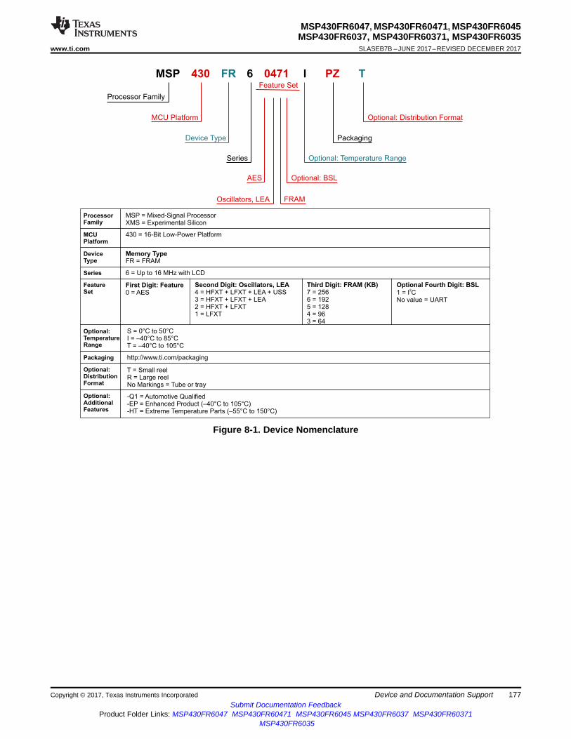
ProcessorFamily
MSP = Mixed-Signal ProcessorXMS = Experimental Silicon
MCUPlatform
430 = 16-Bit Low-Power Platform
DeviceType
Memory TypeFR = FRAM
Series 6 = p to 16 MHz with LCDU
FeatureSet
First Digit: Feature0 = AES
Second Digit: Oscillators, LEA4 = HFXT + LFXT + LEA + USS3 = HFXT + LFXT + LEA2 = HFXT + LFXT1 = LFXT
Third Digit: FRAM (KB)7 = 2566 = 1925 = 1284 = 963 = 64
Optional Fourth Digit: BSL1 = I CNo value = UART
2
Optional:TemperatureRange
Packaging http://www.ti.com/packaging
Optional:DistributionFormat
Optional:AdditionalFeatures
-Q1 =-EP = Enhanced Product (–40°C to 105°C)-HT = Extreme Temperature Parts (–55°C to 150°C)
Automotive Qualified
T = Small reelR = Large reelNo Markings = Tube or tray
S = 0°C to 50 CI = –40 C to 85 CT = –40 C to 105 C
°° °° °
Feature Set
Series
Processor Family
Optional: Temperature Range
MCU Platform
Device Type
Optional: Distribution Format
Packaging
MSP 430 FR 6 0471 I PZ T
Optional: BSL
FRAM
AES
Oscillators, LEA
177
MSP430FR6047, MSP430FR60471, MSP430FR6045MSP430FR6037, MSP430FR60371, MSP430FR6035
www.ti.com SLASEB7B –JUNE 2017–REVISED DECEMBER 2017
Submit Documentation FeedbackProduct Folder Links: MSP430FR6047 MSP430FR60471 MSP430FR6045 MSP430FR6037 MSP430FR60371
MSP430FR6035
Device and Documentation SupportCopyright © 2017, Texas Instruments Incorporated
Figure 8-1. Device Nomenclature

178
MSP430FR6047, MSP430FR60471, MSP430FR6045MSP430FR6037, MSP430FR60371, MSP430FR6035SLASEB7B –JUNE 2017–REVISED DECEMBER 2017 www.ti.com
Submit Documentation FeedbackProduct Folder Links: MSP430FR6047 MSP430FR60471 MSP430FR6045 MSP430FR6037 MSP430FR60371
MSP430FR6035
Device and Documentation Support Copyright © 2017, Texas Instruments Incorporated
8.3 Tools and SoftwareTable 8-1 lists the debug features supported by these microcontrollers. See the Code Composer Studio™IDE for MSP430 User's Guide for details on the available features. See Advanced Debugging Using theEnhanced Emulation Module (EEM) With Code Composer Studio™ IDE and MSP430™ Advanced PowerOptimizations: ULP Advisor™ Software and EnergyTrace™ Technology for further usage information.
Table 8-1. Hardware Features
MSPARCHITECTURE
4-WIREJTAG
2-WIREJTAG
BREAK-POINTS
(N)
RANGEBREAK-POINTS
CLOCKCONTROL
STATESEQUENCER
TRACEBUFFER
LPMx.5DEBUGGING
SUPPORTEnergyTrace++
MSP430Xv2 Yes Yes 3 Yes Yes No No Yes Yes
Design Kits and Evaluation ModulesMSP430FR6047 Ultrasonic Sensing Evaluation Module The EVM430-FR6047 evaluation kit is a
development platform that can be used to evaluate the performance of the MSP430FR6047for ultrasonic sensing applications (for example, smart water meters).
MSP-TS430PZ100E 100-pin Target Development BoardThe MSP-TS430PZ100E is a stand-alone 100-pin ZIF socket target board used to program and debug the MSP430 MCU in-system throughthe JTAG interface or the Spy Bi-Wire (2-wire JTAG) protocol.
SoftwareMSP430Ware™ Software MSP430Ware software is a collection of code examples, data sheets, and
other design resources for all MSP430 devices delivered in a convenient package. Inaddition to providing a complete collection of existing MSP430 design resources,MSP430Ware software also includes a high-level API called MSP430 Driver Library. Thislibrary makes it easy to program MSP430 hardware. MSP430Ware software is available as acomponent of Code Composer Studio IDE or as a stand-alone package.
MSP430FR604x(1), MSP430FR603x(1) Code Examples C Code examples are available for every MSPdevice that configures each of the integrated peripherals for various application needs.
MSP Driver Library Driver Library's abstracted API keeps you above the bits and bytes of the MSP430hardware by providing easy-to-use function calls. Thorough documentation is deliveredthrough a helpful API Guide, which includes details on each function call and the recognizedparameters. Developers can use Driver Library functions to write complete projects withminimal overhead.
MSP EnergyTrace™ Technology EnergyTrace technology for MSP430 microcontrollers is an energy-based code analysis tool that measures and displays the energy profile of the applicationand helps to optimize it for ultra-low-power consumption.
ULP (Ultra-Low Power) Advisor ULP Advisor™ software is a tool for guiding developers to write moreefficient code to fully use the unique ultra-low power features of MSP430 and MSP432microcontrollers. Aimed at both experienced and new microcontroller developers, ULPAdvisor checks your code against a thorough ULP checklist to squeeze every last nano ampout of your application. At build time, ULP Advisor provides notifications and remarks onareas of your code that can be further optimized for lower power.
Fixed-Point Math Library for MSP MCUs The MSP IQmath and Qmath Libraries are a collection ofhighly optimized and high-precision mathematical functions for C programmers to seamlesslyport a floating-point algorithm into fixed-point code on MSP430 and MSP432 devices. Theseroutines are typically used in computationally intensive real-time applications where optimalexecution speed, high accuracy, and ultra-low energy are critical. By using the IQmath andQmath libraries, it is possible to achieve execution speeds considerably faster and energyconsumption considerably lower than equivalent code written using floating-point math.
Floating-Point Math Library for MSP430™ MCUs Continuing to innovate in the low power and low costmicrocontroller space, TI brings you MSPMATHLIB. Leveraging the intelligent peripherals ofour devices, this floating point math library of scalar functions brings you up to 26x betterperformance. Mathlib is easy to integrate into your designs. This library is free and isintegrated in both Code Composer Studio and IAR IDEs. Read the user's guide for an indepth look at the math library and relevant benchmarks.

179
MSP430FR6047, MSP430FR60471, MSP430FR6045MSP430FR6037, MSP430FR60371, MSP430FR6035
www.ti.com SLASEB7B –JUNE 2017–REVISED DECEMBER 2017
Submit Documentation FeedbackProduct Folder Links: MSP430FR6047 MSP430FR60471 MSP430FR6045 MSP430FR6037 MSP430FR60371
MSP430FR6035
Device and Documentation SupportCopyright © 2017, Texas Instruments Incorporated
Development ToolsCode Composer Studio™ Integrated Development Environment for MSP Microcontrollers Code
Composer Studio is an integrated development environment (IDE) that supports all MSPmicrocontroller devices. Code Composer Studio comprises a suite of embedded softwareutilities used to develop and debug embedded applications. It includes an optimizing C/C++compiler, source code editor, project build environment, debugger, profiler, and many otherfeatures. The intuitive IDE provides a single user interface taking you through each step ofthe application development flow. Familiar utilities and interfaces allow users to get startedfaster than ever before. Code Composer Studio combines the advantages of the Eclipsesoftware framework with advanced embedded debug capabilities from TI resulting in acompelling feature-rich development environment for embedded developers. When usingCCS with an MSP MCU, a unique and powerful set of plugins and embedded softwareutilities are made available to fully leverage the MSP microcontroller.
Command-Line Programmer MSP Flasher is an open-source shell-based interface for programmingMSP microcontrollers through a FET programmer or eZ430 using JTAG or Spy-Bi-Wire(SBW) communication. MSP Flasher can download binary files (.txt or .hex) files directly tothe MSP microcontroller without an IDE.
MSP MCU Programmer and Debugger The MSP-FET is a powerful emulation development tool – oftencalled a debug probe – which allows users to quickly begin application development on MSPlow-power microcontrollers (MCU). Creating MCU software usually requires downloading theresulting binary program to the MSP device for validation and debugging. The MSP-FETprovides a debug communication pathway between a host computer and the target MSP.Furthermore, the MSP-FET also provides a Backchannel UART connection between thecomputer's USB interface and the MSP UART. This affords the MSP programmer aconvenient method for communicating serially between the MSP and a terminal running onthe computer. The MSP-FET also supports loading programs (often called firmware) to theMSP target using the BSL through the UART and I2C communication protocols.
MSP-GANG Production Programmer The MSP Gang Programmer is an MSP430 or MSP432 deviceprogrammer that can program up to eight identical MSP430 or MSP432 Flash or FRAMdevices at the same time. The MSP Gang Programmer connects to a host PC using astandard RS-232 or USB connection and provides flexible programming options that allowthe user to fully customize the process. The MSP Gang Programmer is provided with anexpansion board, called the Gang Splitter, that implements the interconnections between theMSP Gang Programmer and multiple target devices. Eight cables are provided that connectthe expansion board to eight target devices (through JTAG or Spy-Bi-Wire connectors). Theprogramming can be done with a PC or as a stand-alone device. A PC-side graphical userinterface is also available and is DLL-based.
8.4 Documentation SupportThe following documents describe the MSP430FR604x(1), MSP430FR603x(1) MCUs. Copies of thesedocuments are available on the Internet at www.ti.com.
Receiving Notification of Document Updates
To receive notification of documentation updates—including silicon errata—go to the product folder foryour device on ti.com (for links to the product folders, see Section 8.5). In the upper-right corner, click the"Alert me" button. This registers you to receive a weekly digest of product information that has changed (ifany). For change details, check the revision history of any revised document.
ErrataMSP430FR6047 Device Erratasheet Describes the known exceptions to the functional specifications.MSP430FR60471 Device Erratasheet Describes the known exceptions to the functional specifications.MSP430FR6045 Device Erratasheet Describes the known exceptions to the functional specifications.MSP430FR6037 Device Erratasheet Describes the known exceptions to the functional specifications.MSP430FR60371 Device Erratasheet Describes the known exceptions to the functional specifications.MSP430FR6035 Device Erratasheet Describes the known exceptions to the functional specifications.
180
MSP430FR6047, MSP430FR60471, MSP430FR6045MSP430FR6037, MSP430FR60371, MSP430FR6035SLASEB7B –JUNE 2017–REVISED DECEMBER 2017 www.ti.com
Submit Documentation FeedbackProduct Folder Links: MSP430FR6047 MSP430FR60471 MSP430FR6045 MSP430FR6037 MSP430FR60371
MSP430FR6035
Device and Documentation Support Copyright © 2017, Texas Instruments Incorporated
User's GuidesMSP430FR58xx, MSP430FR59xx, and MSP430FR6xx Family User's GuideDetailed description of all
modules and peripherals available in this device family.MSP430™ FRAM Devices Bootloader (BSL) User's Guide The bootloader (BSL) on MSP430
microcontrollers (MCUs) lets users communicate with embedded memory in the MSP430MCU during the prototyping phase, final production, and in service. Both the programmablememory (FRAM memory) and the data memory (RAM) can be modified as required.
MSP430™ Programming With the JTAG Interface This document describes the functions that arerequired to erase, program, and verify the memory module of the MSP430 flash-based andFRAM-based microcontroller families using the JTAG communication port. In addition, itdescribes how to program the JTAG access security fuse that is available on all MSP430devices. This document describes device access using both the standard 4-wire JTAGinterface and the 2-wire JTAG interface, which is also referred to as Spy-Bi-Wire (SBW).
MSP430™ Hardware Tools User's Guide This manual describes the hardware of the TI MSP-FET430Flash Emulation Tool (FET). The FET is the program development tool for the MSP430 ultra-low-power microcontroller.
Application ReportsMSP430™ 32-kHz Crystal Oscillators Selection of the correct crystal, correct load circuit, and proper
board layout are important for a stable crystal oscillator. This application report summarizescrystal oscillator function and explains the parameters to select the correct crystal forMSP430 ultra-low-power operation. In addition, hints and examples for correct board layoutare given. The document also contains detailed information on the possible oscillator tests toensure stable oscillator operation in mass production.
MSP430™ System-Level ESD Considerations System-Level ESD has become increasingly demandingwith silicon technology scaling towards lower voltages and the need for designing cost-effective and ultra-low-power components. This application report addresses three differentESD topics to help board designers and OEMs understand and design robust system-leveldesigns: (1) Component-level ESD testing and system-level ESD testing, their differencesand why component-level ESD rating does not ensure system-level robustness. (2) Generaldesign guidelines for system-level ESD protection at different levels including enclosures,cables, PCB layout, and onboard ESD protection devices. (3) Introduction to System EfficientESD Design (SEED), a codesign methodology of onboard and on-chip ESD protection toachieve system-level ESD robustness, with example simulations and test results. A few real-world system-level ESD protection design examples and their results are also discussed.
8.5 Related LinksTable 8-2 lists quick access links. Categories include technical documents, support and communityresources, tools and software, and quick access to order now.
Table 8-2. Related Links
PARTS PRODUCT FOLDER ORDER NOW TECHNICALDOCUMENTS
TOOLS &SOFTWARE
SUPPORT &COMMUNITY
MSP430FR6047 Click here Click here Click here Click here Click hereMSP430FR60471 Click here Click here Click here Click here Click hereMSP430FR6045 Click here Click here Click here Click here Click hereMSP430FR6037 Click here Click here Click here Click here Click hereMSP430FR60371 Click here Click here Click here Click here Click hereMSP430FR6035 Click here Click here Click here Click here Click here
8.6 TrademarksMSP430Ware, MSP430, EnergyTrace, ULP Advisor, Code Composer Studio are trademarks of TexasInstruments.Arm, Cortex are registered trademarks of Arm Limited.Microsoft is a registered trademark of Microsoft Corporation.All other trademarks are the property of their respective owners.

181
MSP430FR6047, MSP430FR60471, MSP430FR6045MSP430FR6037, MSP430FR60371, MSP430FR6035
www.ti.com SLASEB7B –JUNE 2017–REVISED DECEMBER 2017
Submit Documentation FeedbackProduct Folder Links: MSP430FR6047 MSP430FR60471 MSP430FR6045 MSP430FR6037 MSP430FR60371
MSP430FR6035
Mechanical, Packaging, and Orderable InformationCopyright © 2017, Texas Instruments Incorporated
8.7 Electrostatic Discharge CautionThis integrated circuit can be damaged by ESD. Texas Instruments recommends that all integrated circuits be handled withappropriate precautions. Failure to observe proper handling and installation procedures can cause damage.
ESD damage can range from subtle performance degradation to complete device failure. Precision integrated circuits may be moresusceptible to damage because very small parametric changes could cause the device not to meet its published specifications.
8.8 Export Control NoticeRecipient agrees to not knowingly export or re-export, directly or indirectly, any product or technical data(as defined by the U.S., EU, and other Export Administration Regulations) including software, or anycontrolled product restricted by other applicable national regulations, received from disclosing party undernondisclosure obligations (if any), or any direct product of such technology, to any destination to whichsuch export or re-export is restricted or prohibited by U.S. or other applicable laws, without obtaining priorauthorization from U.S. Department of Commerce and other competent Government authorities to theextent required by those laws.
8.9 GlossaryTI Glossary This glossary lists and explains terms, acronyms, and definitions.
9 Mechanical, Packaging, and Orderable Information
The following pages include mechanical, packaging, and orderable information. This information is themost current data available for the designated devices. This data is subject to change without notice andrevision of this document. For browser-based versions of this data sheet, refer to the left-hand navigation.
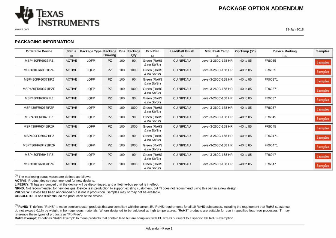
PACKAGE OPTION ADDENDUM
www.ti.com 12-Jan-2018
Addendum-Page 1
PACKAGING INFORMATION
Orderable Device Status(1)
Package Type PackageDrawing
Pins PackageQty
Eco Plan(2)
Lead/Ball Finish(6)
MSL Peak Temp(3)
Op Temp (°C) Device Marking(4/5)
Samples
MSP430FR6035IPZ ACTIVE LQFP PZ 100 90 Green (RoHS& no Sb/Br)
CU NIPDAU Level-3-260C-168 HR -40 to 85 FR6035
MSP430FR6035IPZR ACTIVE LQFP PZ 100 1000 Green (RoHS& no Sb/Br)
CU NIPDAU Level-3-260C-168 HR -40 to 85 FR6035
MSP430FR60371IPZ ACTIVE LQFP PZ 100 90 Green (RoHS& no Sb/Br)
CU NIPDAU Level-3-260C-168 HR -40 to 85 FR60371
MSP430FR60371IPZR ACTIVE LQFP PZ 100 1000 Green (RoHS& no Sb/Br)
CU NIPDAU Level-3-260C-168 HR -40 to 85 FR60371
MSP430FR6037IPZ ACTIVE LQFP PZ 100 90 Green (RoHS& no Sb/Br)
CU NIPDAU Level-3-260C-168 HR -40 to 85 FR6037
MSP430FR6037IPZR ACTIVE LQFP PZ 100 1000 Green (RoHS& no Sb/Br)
CU NIPDAU Level-3-260C-168 HR -40 to 85 FR6037
MSP430FR6045IPZ ACTIVE LQFP PZ 100 90 Green (RoHS& no Sb/Br)
CU NIPDAU Level-3-260C-168 HR -40 to 85 FR6045
MSP430FR6045IPZR ACTIVE LQFP PZ 100 1000 Green (RoHS& no Sb/Br)
CU NIPDAU Level-3-260C-168 HR -40 to 85 FR6045
MSP430FR60471IPZ ACTIVE LQFP PZ 100 90 Green (RoHS& no Sb/Br)
CU NIPDAU Level-3-260C-168 HR -40 to 85 FR60471
MSP430FR60471IPZR ACTIVE LQFP PZ 100 1000 Green (RoHS& no Sb/Br)
CU NIPDAU Level-3-260C-168 HR -40 to 85 FR60471
MSP430FR6047IPZ ACTIVE LQFP PZ 100 90 Green (RoHS& no Sb/Br)
CU NIPDAU Level-3-260C-168 HR -40 to 85 FR6047
MSP430FR6047IPZR ACTIVE LQFP PZ 100 1000 Green (RoHS& no Sb/Br)
CU NIPDAU Level-3-260C-168 HR -40 to 85 FR6047
(1) The marketing status values are defined as follows:ACTIVE: Product device recommended for new designs.LIFEBUY: TI has announced that the device will be discontinued, and a lifetime-buy period is in effect.NRND: Not recommended for new designs. Device is in production to support existing customers, but TI does not recommend using this part in a new design.PREVIEW: Device has been announced but is not in production. Samples may or may not be available.OBSOLETE: TI has discontinued the production of the device.
(2) RoHS: TI defines "RoHS" to mean semiconductor products that are compliant with the current EU RoHS requirements for all 10 RoHS substances, including the requirement that RoHS substancedo not exceed 0.1% by weight in homogeneous materials. Where designed to be soldered at high temperatures, "RoHS" products are suitable for use in specified lead-free processes. TI mayreference these types of products as "Pb-Free".RoHS Exempt: TI defines "RoHS Exempt" to mean products that contain lead but are compliant with EU RoHS pursuant to a specific EU RoHS exemption.

PACKAGE OPTION ADDENDUM
www.ti.com 12-Jan-2018
Addendum-Page 2
Green: TI defines "Green" to mean the content of Chlorine (Cl) and Bromine (Br) based flame retardants meet JS709B low halogen requirements of <=1000ppm threshold. Antimony trioxide basedflame retardants must also meet the <=1000ppm threshold requirement.
(3) MSL, Peak Temp. - The Moisture Sensitivity Level rating according to the JEDEC industry standard classifications, and peak solder temperature.
(4) There may be additional marking, which relates to the logo, the lot trace code information, or the environmental category on the device.
(5) Multiple Device Markings will be inside parentheses. Only one Device Marking contained in parentheses and separated by a "~" will appear on a device. If a line is indented then it is a continuationof the previous line and the two combined represent the entire Device Marking for that device.
(6) Lead/Ball Finish - Orderable Devices may have multiple material finish options. Finish options are separated by a vertical ruled line. Lead/Ball Finish values may wrap to two lines if the finishvalue exceeds the maximum column width.
Important Information and Disclaimer:The information provided on this page represents TI's knowledge and belief as of the date that it is provided. TI bases its knowledge and belief on informationprovided by third parties, and makes no representation or warranty as to the accuracy of such information. Efforts are underway to better integrate information from third parties. TI has taken andcontinues to take reasonable steps to provide representative and accurate information but may not have conducted destructive testing or chemical analysis on incoming materials and chemicals.TI and TI suppliers consider certain information to be proprietary, and thus CAS numbers and other limited information may not be available for release.
In no event shall TI's liability arising out of such information exceed the total purchase price of the TI part(s) at issue in this document sold by TI to Customer on an annual basis.

TAPE AND REEL INFORMATION
*All dimensions are nominal
Device PackageType
PackageDrawing
Pins SPQ ReelDiameter
(mm)
ReelWidth
W1 (mm)
A0(mm)
B0(mm)
K0(mm)
P1(mm)
W(mm)
Pin1Quadrant
MSP430FR6035IPZR LQFP PZ 100 1000 330.0 24.4 17.0 17.0 2.1 20.0 24.0 Q2
MSP430FR60371IPZR LQFP PZ 100 1000 330.0 24.4 17.0 17.0 2.1 20.0 24.0 Q2
MSP430FR6037IPZR LQFP PZ 100 1000 330.0 24.4 17.0 17.0 2.1 20.0 24.0 Q2
MSP430FR6045IPZR LQFP PZ 100 1000 330.0 24.4 17.0 17.0 2.1 20.0 24.0 Q2
MSP430FR60471IPZR LQFP PZ 100 1000 330.0 24.4 17.0 17.0 2.1 20.0 24.0 Q2
MSP430FR6047IPZR LQFP PZ 100 1000 330.0 24.4 17.0 17.0 2.1 20.0 24.0 Q2
PACKAGE MATERIALS INFORMATION
www.ti.com 18-Dec-2017
Pack Materials-Page 1
*All dimensions are nominal
Device Package Type Package Drawing Pins SPQ Length (mm) Width (mm) Height (mm)
MSP430FR6035IPZR LQFP PZ 100 1000 367.0 367.0 45.0
MSP430FR60371IPZR LQFP PZ 100 1000 367.0 367.0 45.0
MSP430FR6037IPZR LQFP PZ 100 1000 367.0 367.0 45.0
MSP430FR6045IPZR LQFP PZ 100 1000 367.0 367.0 45.0
MSP430FR60471IPZR LQFP PZ 100 1000 367.0 367.0 45.0
MSP430FR6047IPZR LQFP PZ 100 1000 367.0 367.0 45.0
PACKAGE MATERIALS INFORMATION
www.ti.com 18-Dec-2017
Pack Materials-Page 2

MECHANICAL DATA
MTQF013A – OCTOBER 1994 – REVISED DECEMBER 1996
1POST OFFICE BOX 655303 • DALLAS, TEXAS 75265
PZ (S-PQFP-G100) PLASTIC QUAD FLATPACK
4040149/B 11/96
50
26 0,13 NOM
Gage Plane
0,25
0,450,75
0,05 MIN
0,27
51
25
75
1
12,00 TYP
0,17
76
100
SQ
SQ15,8016,20
13,80
1,351,45
1,60 MAX
14,20
0°–7°
Seating Plane
0,08
0,50 M0,08
NOTES: A. All linear dimensions are in millimeters.B. This drawing is subject to change without notice.C. Falls within JEDEC MS-026

IMPORTANT NOTICE
Texas Instruments Incorporated (TI) reserves the right to make corrections, enhancements, improvements and other changes to itssemiconductor products and services per JESD46, latest issue, and to discontinue any product or service per JESD48, latest issue. Buyersshould obtain the latest relevant information before placing orders and should verify that such information is current and complete.TI’s published terms of sale for semiconductor products (http://www.ti.com/sc/docs/stdterms.htm) apply to the sale of packaged integratedcircuit products that TI has qualified and released to market. Additional terms may apply to the use or sale of other types of TI products andservices.Reproduction of significant portions of TI information in TI data sheets is permissible only if reproduction is without alteration and isaccompanied by all associated warranties, conditions, limitations, and notices. TI is not responsible or liable for such reproduceddocumentation. Information of third parties may be subject to additional restrictions. Resale of TI products or services with statementsdifferent from or beyond the parameters stated by TI for that product or service voids all express and any implied warranties for theassociated TI product or service and is an unfair and deceptive business practice. TI is not responsible or liable for any such statements.Buyers and others who are developing systems that incorporate TI products (collectively, “Designers”) understand and agree that Designersremain responsible for using their independent analysis, evaluation and judgment in designing their applications and that Designers havefull and exclusive responsibility to assure the safety of Designers' applications and compliance of their applications (and of all TI productsused in or for Designers’ applications) with all applicable regulations, laws and other applicable requirements. Designer represents that, withrespect to their applications, Designer has all the necessary expertise to create and implement safeguards that (1) anticipate dangerousconsequences of failures, (2) monitor failures and their consequences, and (3) lessen the likelihood of failures that might cause harm andtake appropriate actions. Designer agrees that prior to using or distributing any applications that include TI products, Designer willthoroughly test such applications and the functionality of such TI products as used in such applications.TI’s provision of technical, application or other design advice, quality characterization, reliability data or other services or information,including, but not limited to, reference designs and materials relating to evaluation modules, (collectively, “TI Resources”) are intended toassist designers who are developing applications that incorporate TI products; by downloading, accessing or using TI Resources in anyway, Designer (individually or, if Designer is acting on behalf of a company, Designer’s company) agrees to use any particular TI Resourcesolely for this purpose and subject to the terms of this Notice.TI’s provision of TI Resources does not expand or otherwise alter TI’s applicable published warranties or warranty disclaimers for TIproducts, and no additional obligations or liabilities arise from TI providing such TI Resources. TI reserves the right to make corrections,enhancements, improvements and other changes to its TI Resources. TI has not conducted any testing other than that specificallydescribed in the published documentation for a particular TI Resource.Designer is authorized to use, copy and modify any individual TI Resource only in connection with the development of applications thatinclude the TI product(s) identified in such TI Resource. NO OTHER LICENSE, EXPRESS OR IMPLIED, BY ESTOPPEL OR OTHERWISETO ANY OTHER TI INTELLECTUAL PROPERTY RIGHT, AND NO LICENSE TO ANY TECHNOLOGY OR INTELLECTUAL PROPERTYRIGHT OF TI OR ANY THIRD PARTY IS GRANTED HEREIN, including but not limited to any patent right, copyright, mask work right, orother intellectual property right relating to any combination, machine, or process in which TI products or services are used. Informationregarding or referencing third-party products or services does not constitute a license to use such products or services, or a warranty orendorsement thereof. Use of TI Resources may require a license from a third party under the patents or other intellectual property of thethird party, or a license from TI under the patents or other intellectual property of TI.TI RESOURCES ARE PROVIDED “AS IS” AND WITH ALL FAULTS. TI DISCLAIMS ALL OTHER WARRANTIES ORREPRESENTATIONS, EXPRESS OR IMPLIED, REGARDING RESOURCES OR USE THEREOF, INCLUDING BUT NOT LIMITED TOACCURACY OR COMPLETENESS, TITLE, ANY EPIDEMIC FAILURE WARRANTY AND ANY IMPLIED WARRANTIES OFMERCHANTABILITY, FITNESS FOR A PARTICULAR PURPOSE, AND NON-INFRINGEMENT OF ANY THIRD PARTY INTELLECTUALPROPERTY RIGHTS. TI SHALL NOT BE LIABLE FOR AND SHALL NOT DEFEND OR INDEMNIFY DESIGNER AGAINST ANY CLAIM,INCLUDING BUT NOT LIMITED TO ANY INFRINGEMENT CLAIM THAT RELATES TO OR IS BASED ON ANY COMBINATION OFPRODUCTS EVEN IF DESCRIBED IN TI RESOURCES OR OTHERWISE. IN NO EVENT SHALL TI BE LIABLE FOR ANY ACTUAL,DIRECT, SPECIAL, COLLATERAL, INDIRECT, PUNITIVE, INCIDENTAL, CONSEQUENTIAL OR EXEMPLARY DAMAGES INCONNECTION WITH OR ARISING OUT OF TI RESOURCES OR USE THEREOF, AND REGARDLESS OF WHETHER TI HAS BEENADVISED OF THE POSSIBILITY OF SUCH DAMAGES.Unless TI has explicitly designated an individual product as meeting the requirements of a particular industry standard (e.g., ISO/TS 16949and ISO 26262), TI is not responsible for any failure to meet such industry standard requirements.Where TI specifically promotes products as facilitating functional safety or as compliant with industry functional safety standards, suchproducts are intended to help enable customers to design and create their own applications that meet applicable functional safety standardsand requirements. Using products in an application does not by itself establish any safety features in the application. Designers mustensure compliance with safety-related requirements and standards applicable to their applications. Designer may not use any TI products inlife-critical medical equipment unless authorized officers of the parties have executed a special contract specifically governing such use.Life-critical medical equipment is medical equipment where failure of such equipment would cause serious bodily injury or death (e.g., lifesupport, pacemakers, defibrillators, heart pumps, neurostimulators, and implantables). Such equipment includes, without limitation, allmedical devices identified by the U.S. Food and Drug Administration as Class III devices and equivalent classifications outside the U.S.TI may expressly designate certain products as completing a particular qualification (e.g., Q100, Military Grade, or Enhanced Product).Designers agree that it has the necessary expertise to select the product with the appropriate qualification designation for their applicationsand that proper product selection is at Designers’ own risk. Designers are solely responsible for compliance with all legal and regulatoryrequirements in connection with such selection.Designer will fully indemnify TI and its representatives against any damages, costs, losses, and/or liabilities arising out of Designer’s non-compliance with the terms and provisions of this Notice.
Mailing Address: Texas Instruments, Post Office Box 655303, Dallas, Texas 75265Copyright © 2018, Texas Instruments Incorporated
Related Documents


