Freescale Semiconductor Application Note © Freescale Semiconductor, Inc., 2007. All rights reserved. This application note explains how to configure and run Ethernet-based applications on the MSC8144 DSP to maximize performance and minimize overhead. The example code in the .zip file that accompanies this document is based on the SmartDSP operating system (OS) running on the MSC8144 application development system (MSC8144ADS). After reading this application note, you should understand: • How Ethernet works on the MSC8144 system • How to use and configure SmartDSP OS for the MSC8144 to attain the highest throughput for Ethernet-dependent applications • What performance numbers to expect for different Ethernet configurations Using the MSC8144ADS and the example applications from SmartDSP OS, which are provided with CodeWarrior™ v3.0, you can easily replicate the behavior and performance of MSC8144 Ethernet as described here. Although this application note is directed to the MSC8144 DSP, it also applies to the MSC8144E and MSC8144EC. Document Number: AN3439 Rev. 0, 09/2007 Contents 1 Ethernet Basics . . . . . . . . . . . . . . . . . . . . . . . . . . . . . . . 2 2 Ethernet Architecture for the MSC8144 . . . . . . . . . . . . 3 2.1 QUICC Engine . . . . . . . . . . . . . . . . . . . . . . . . . . . . . . . 3 2.2 Ethernet Controllers . . . . . . . . . . . . . . . . . . . . . . . . . . . 5 3 Ethernet Controller (UEC) Frame Filtering . . . . . . . . . 6 3.1 MPC82xx Filtering Mode . . . . . . . . . . . . . . . . . . . . . . . 6 3.2 Extended Parsing Mode . . . . . . . . . . . . . . . . . . . . . . . . 6 4 Ethernet Performance Testing on the MSC8144ADS .8 4.1 SmartBits . . . . . . . . . . . . . . . . . . . . . . . . . . . . . . . . . . . 8 4.2 MSC8144ADS Board . . . . . . . . . . . . . . . . . . . . . . . . . 10 4.3 SmartDSP OS Software and Demos . . . . . . . . . . . . . . 11 5 Performance Testing . . . . . . . . . . . . . . . . . . . . . . . . . . 11 5.1 Testing with UDP Echo . . . . . . . . . . . . . . . . . . . . . . . 11 5.2 Testing L2 Ethernet Echo . . . . . . . . . . . . . . . . . . . . . . 34 6 Maximizing the QUICC Engine Throughput . . . . . . . 41 6.1 MPC82xx Filtering . . . . . . . . . . . . . . . . . . . . . . . . . . . 41 6.2 Extended Parsing Mode . . . . . . . . . . . . . . . . . . . . . . . 44 6.3 Four Cores in Extended Parsing Mode . . . . . . . . . . . . 44 6.4 Performance Measurement Summary . . . . . . . . . . . . . 45 7 Revision History . . . . . . . . . . . . . . . . . . . . . . . . . . . . . 47 MSC8144 Ethernet Performance Maximizing QUICC Engine™ Throughput by Andrew Temple NCSG DSP Applications Freescale Semiconductor, Inc. Austin, TX

Welcome message from author
This document is posted to help you gain knowledge. Please leave a comment to let me know what you think about it! Share it to your friends and learn new things together.
Transcript
Freescale SemiconductorApplication Note
© Freescale Semiconductor, Inc., 2007. All rights reserved.
This application note explains how to configure and run Ethernet-based applications on the MSC8144 DSP to maximize performance and minimize overhead. The example code in the .zip file that accompanies this document is based on the SmartDSP operating system (OS) running on the MSC8144 application development system (MSC8144ADS). After reading this application note, you should understand:
• How Ethernet works on the MSC8144 system• How to use and configure SmartDSP OS for the
MSC8144 to attain the highest throughput for Ethernet-dependent applications
• What performance numbers to expect for different Ethernet configurations
Using the MSC8144ADS and the example applications from SmartDSP OS, which are provided with CodeWarrior™ v3.0, you can easily replicate the behavior and performance of MSC8144 Ethernet as described here. Although this application note is directed to the MSC8144 DSP, it also applies to the MSC8144E and MSC8144EC.
Document Number: AN3439Rev. 0, 09/2007
Contents1 Ethernet Basics . . . . . . . . . . . . . . . . . . . . . . . . . . . . . . .22 Ethernet Architecture for the MSC8144 . . . . . . . . . . . .32.1 QUICC Engine . . . . . . . . . . . . . . . . . . . . . . . . . . . . . . .32.2 Ethernet Controllers . . . . . . . . . . . . . . . . . . . . . . . . . . .5
3 Ethernet Controller (UEC) Frame Filtering . . . . . . . . .63.1 MPC82xx Filtering Mode . . . . . . . . . . . . . . . . . . . . . . .63.2 Extended Parsing Mode . . . . . . . . . . . . . . . . . . . . . . . .6
4 Ethernet Performance Testing on the MSC8144ADS .84.1 SmartBits . . . . . . . . . . . . . . . . . . . . . . . . . . . . . . . . . . .84.2 MSC8144ADS Board . . . . . . . . . . . . . . . . . . . . . . . . .104.3 SmartDSP OS Software and Demos . . . . . . . . . . . . . .11
5 Performance Testing . . . . . . . . . . . . . . . . . . . . . . . . . .115.1 Testing with UDP Echo . . . . . . . . . . . . . . . . . . . . . . .115.2 Testing L2 Ethernet Echo . . . . . . . . . . . . . . . . . . . . . .34
6 Maximizing the QUICC Engine Throughput . . . . . . .416.1 MPC82xx Filtering . . . . . . . . . . . . . . . . . . . . . . . . . . .416.2 Extended Parsing Mode . . . . . . . . . . . . . . . . . . . . . . .446.3 Four Cores in Extended Parsing Mode . . . . . . . . . . . .446.4 Performance Measurement Summary . . . . . . . . . . . . .45
7 Revision History . . . . . . . . . . . . . . . . . . . . . . . . . . . . .47
MSC8144 Ethernet PerformanceMaximizing QUICC Engine™ Throughput
by Andrew TempleNCSG DSP ApplicationsFreescale Semiconductor, Inc.Austin, TX

MSC8144 Ethernet Performance, Rev. 0
2 Freescale Semiconductor
Ethernet Basics
1 Ethernet BasicsA consideration of Ethernet packetization and the Internet protocol stack is relevant to the task of optimizing the way Ethernet interacts with the MSC8144 DSP within a system. Data is sent through the Ethernet in packets that abstract to different layers of the Internet protocol suite. These packets have different sizes and structures so that the receiver can abstract the information if the receiver is configured to handle the protocols and layers in the packet. Figure 1 depicts the layers of the Internet protocol suite.
Figure 1. Internet Protocol Suite
Some layers of the protocol stack have multiple protocols to select. For example, the Transport layer has both TCP and UDP. Protocols can vary greatly in the complexity of the algorithm, system load required, and packet size. You should consider these differences when designing an application for a system that is performance sensitive.
The layers of the protocol stack are put together in an actual data packet by taking the assembled packet from the layer above and then adding transmit, encode, encryption, or error checking information to the front. This process repeats at each layer until it reaches the physical layer where the data is actually transmitted. There are a few exceptions to this flow. For example, ARP is not included in packets stemming from layers above it, and ICMP is actually a mini-layer above IP. However, the overall process moves down through the protocol layers. So naturally, if packet size is an issue, the goal of the programmer/designer should be to start as close to the physical layer as possible in building packets.
For example, in Figure 2, the IP protocol requires the fields from Version down to Destination IP Address, and then the data follows. If the full packet is a TCP packet, the data contains a set of required communication fields in addition to the actual payload data.
Application
Presentation
Session
Transport
Network
Link
Physical Ethernet
ARP, RARP
Routing Protocols, IP, ICMP
TCP, UDP
Telnet,
SNMP,SMTP,
NFS
XDR
RPC
Layers Protocols
RTP

MSC8144 Ethernet Performance, Rev. 0
Freescale Semiconductor 3
Ethernet Architecture for the MSC8144
2 Ethernet Architecture for the MSC8144The MSC8144 device is a quad-core Freescale StarCore® DSP device, the next generation after the MSC8122. The MSC8144 is intended for a wide range of Ethernet-dependent applications, including VoIP, media gateway, and wireless base station. Currently, many applications pertaining to real-time voice and streaming video use RTCP/RTP service to transmit digitized voice and video. RTP sits on top of UDP in the Internet protocol suite and provides feedback to the sender about the quality of the data distribution over the network. What RTP does not do is cause the sender to regenerate packets or slow down the actual system. When real-time data or voice is transmitted and a voice or video packet is not received, it usually cannot be re-used at a later time. Therefore, the packet is discarded and the TCP protocol is usually not necessary, which lessens the load on the system. Instead, UDP can be used, which simply transmits packets to a destination IP address without the overhead of TCP caused by disassembling and reassembling data, requiring acknowledgement, and flow control.
Therefore, in the discussion of testing the MSC8144 Ethernet, and considering the overhead of the Internet protocol suite, this application note simply focuses on the layers used by RTP: UDP, IP, and raw Ethernet performance. It does not consider the complicated protocols based on TCP.
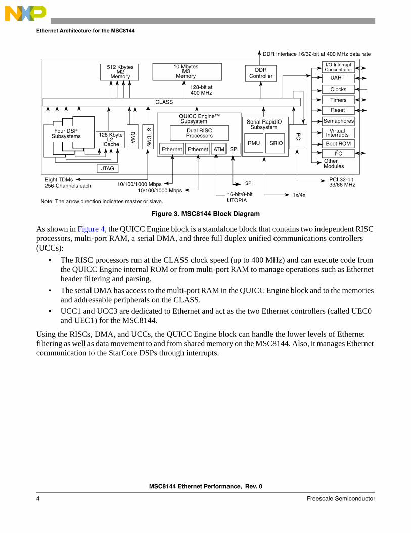
In analyzing the MSC8144 Ethernet performance and bottlenecks, an overall understanding of the MSC8144 architecture as it pertains to the Ethernet is essential. Thus, the remainder of this section takes a look at the MSC8144 architecture (see Figure 3) and then focuses on the QUICC Engine block and the Ethernet controllers.
2.1 QUICC EngineThe MSC8144 uses the QUICC Engine subsystem for Ethernet, ATM, and SPI communication. The block diagram in Figure 3 shows the QUICC Engine block as part of the MSC8144.
32 Bits
Version Header Length Type of Service Total Length (of IP packet+ above layers)
Identification Flags Fragment Offset
Time To Live Protocol (from above Layer)
Header Checksum
Source IP Address
Destination IP Address
Options + Padding
Data (data from layers above IP would be located here)
Figure 2. IP Packet Structure
MSC8144 Ethernet Performance, Rev. 0
4 Freescale Semiconductor
Ethernet Architecture for the MSC8144
Figure 3. MSC8144 Block Diagram
As shown in Figure 4, the QUICC Engine block is a standalone block that contains two independent RISC processors, multi-port RAM, a serial DMA, and three full duplex unified communications controllers (UCCs):
• The RISC processors run at the CLASS clock speed (up to 400 MHz) and can execute code from the QUICC Engine internal ROM or from multi-port RAM to manage operations such as Ethernet header filtering and parsing.
• The serial DMA has access to the multi-port RAM in the QUICC Engine block and to the memories and addressable peripherals on the CLASS.
• UCC1 and UCC3 are dedicated to Ethernet and act as the two Ethernet controllers (called UEC0 and UEC1) for the MSC8144.
Using the RISCs, DMA, and UCCs, the QUICC Engine block can handle the lower levels of Ethernet filtering as well as data movement to and from shared memory on the MSC8144. Also, it manages Ethernet communication to the StarCore DSPs through interrupts.
JTAG
RMU SRIO
Note: The arrow direction indicates master or slave.
128-bit at
DDR Interface 16/32-bit at 400 MHz data rate
8 TD
Ms
DM
A
I/O-InterruptConcentrator
UART
Clocks
Timers
Reset
Semaphores
Other
DDR10 Mbytes
M3Memory
512 KbytesM2
Memory
CLASS
128 KbyteL2
ICache
PC
I
PCI 32-bit
Serial RapidIOSubsystem
Modules
QUICC Engine™
Ethernet
Dual RISC
ATM
16-bit/8-bit
10/100/1000 Mbps10/100/1000 Mbps
Subsystem
400 MHz
Processors
Eight TDMs33/66 MHz
1x/4x
256-Channels each
Four DSP Subsystems
EthernetBoot ROM
I2C
VirtualInterrupts
Controller
UTOPIA
SPI
SPI

MSC8144 Ethernet Performance, Rev. 0
Freescale Semiconductor 5
Ethernet Architecture for the MSC8144
Figure 4. MSC8144 QUICC Engine Block
2.2 Ethernet ControllersThe two UCCs (UCC1 and UCC3) used on the MSC8144 as UCC Ethernet controllers (UECs) support the following physical interfaces for communication:
• MII: 10 and 100 Mbps (supported by only one of the controllers)• RMII: 10 and 100 Mbps • SMII: 10 and 100 Mbps• RGMII: 10, 100, and 1000 Mbps• SGMII: 1000 Mbps
This discussion focuses on RGMII running at 1 Gbps and the maximum throughput of the MSC8144 Ethernet interface. The Ethernet frame is a standard untagged Ethernet frame consisting of a preamble, start frame delimiter, destination and source address, type, and data as shown in Figure 5.
To understand how to tune your code for better Ethernet performance, you must know how the QUICC Engine block and UEC can be used to handle Ethernet frames. Performance measurements in the UEC
7 bytes 1 byte 6 bytes 6 bytes 2 bytes 46-1500 bytes 4 bytes
Preamble Start Frame Delimiter
Dest. Address Source Address Type/Length Data Frame Check Sequence
Figure 5. Untagged Ethernet Frame
ATM Ethernet
UTOPIA L2
Peripheral Bus
SDMAs
Multi-InitiatorRAM 48 KB
RMII/SMII/MIIRGMII/SGMII
Controller Controller
25/50 MHz10/100/1000
EthernetController
RMIIRGMII/SGMII10/100/1000
CLASS
32-Bit
Processor
ROM
RISC32-Bit
Processor
ROM
RISC
IRAM
MSC8144 Ethernet Performance, Rev. 0
6 Freescale Semiconductor
Ethernet Controller (UEC) Frame Filtering
requires that the DSP be notified of errors so that it can offer the user multiple means of detecting dropped frames and causes. The UEC interrupts the DSP (in RGMII mode) for the following messages and errors:
• Lost carrier sense• Underrun• Number of collisions exceeded the maximum allowed• Number of retries per frame• Deferred frame indication• Late collision• Excessive deferred frame indication• CRC error indication• Nonoctet alignment error• Frame too short/long• Overrun• Busy (out of buffers)
3 Ethernet Controller (UEC) Frame FilteringThe QUICC Engine RISC processors provide frame filtering functionality. There are two main types of Ethernet frame filtering: MPC82xx filtering mode and extended parsing mode. The UECs also have a set of extended features (extended features mode) for further frame filtering.
3.1 MPC82xx Filtering ModeMPC82xx filtering mode physically filters incoming frames by MAC destination address. Two 32-bit MAC address registers, called the MAC station address registers, represent a single MAC address assigned to the UEC. If the destination MAC address of an incoming frame does not match the contents of the MAC station address registers and extended features are enabled, the UEC compares the frame’s destination MAC address for a match with one of four more values in the memory-mapped PADDR registers.
In addition, the UEC can be programmed to accept broadcast frames in broadcast mode or to accept all frames in promiscuous mode. All frames are accepted into a single queue, so only one core accesses these frames.
If the UEC is not set up for promiscuous or broadcast mode and a frame address fails a comparison with the contents of the MAC station address and PADDR registers, the frame is discarded.
3.2 Extended Parsing ModeIn extended parsing mode, incoming frames are filtered according to Ethernet layer 2–4 (L2, L3, and L4) contents. These layers are broken down as follows:
• L2: Raw Ethernet layer information: MAC source and destination addresses and the L3 protocol type
• L3: IP layer information: IP source and destination addresses and the L4 protocol type• L4: TCP/UDP layer information: source and destination ports,
MSC8144 Ethernet Performance, Rev. 0
Freescale Semiconductor 7
Ethernet Controller (UEC) Frame Filtering
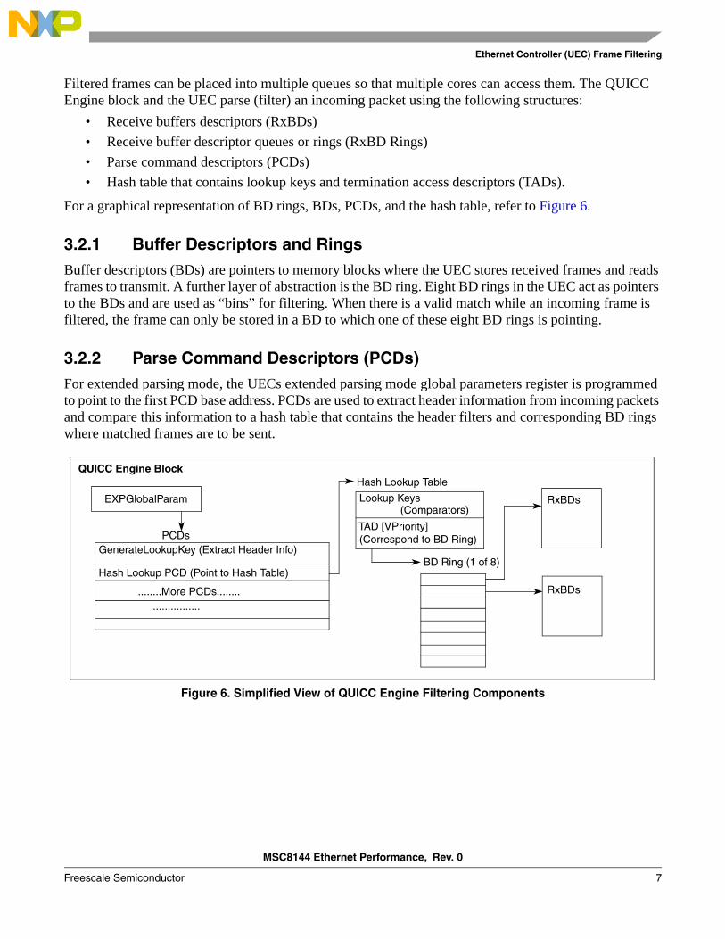
Filtered frames can be placed into multiple queues so that multiple cores can access them. The QUICC Engine block and the UEC parse (filter) an incoming packet using the following structures:
• Receive buffers descriptors (RxBDs)• Receive buffer descriptor queues or rings (RxBD Rings)• Parse command descriptors (PCDs)• Hash table that contains lookup keys and termination access descriptors (TADs).
For a graphical representation of BD rings, BDs, PCDs, and the hash table, refer to Figure 6.
3.2.1 Buffer Descriptors and RingsBuffer descriptors (BDs) are pointers to memory blocks where the UEC stores received frames and reads frames to transmit. A further layer of abstraction is the BD ring. Eight BD rings in the UEC act as pointers to the BDs and are used as “bins” for filtering. When there is a valid match while an incoming frame is filtered, the frame can only be stored in a BD to which one of these eight BD rings is pointing.
3.2.2 Parse Command Descriptors (PCDs)For extended parsing mode, the UECs extended parsing mode global parameters register is programmed to point to the first PCD base address. PCDs are used to extract header information from incoming packets and compare this information to a hash table that contains the header filters and corresponding BD rings where matched frames are to be sent.
Figure 6. Simplified View of QUICC Engine Filtering Components
QUICC Engine Block
EXPGlobalParam
GenerateLookupKey (Extract Header Info)PCDs
Hash Lookup PCD (Point to Hash Table)
........More PCDs........................
Hash Lookup Table
Lookup Keys
TAD [VPriority]
(Comparators)
(Correspond to BD Ring)
BD Ring (1 of 8)
RxBDs
RxBDs
MSC8144 Ethernet Performance, Rev. 0
8 Freescale Semiconductor
Ethernet Performance Testing on the MSC8144ADS
4 Ethernet Performance Testing on the MSC8144ADSTo generate the data represented in this application note, the following equipment was used:
• Spirent Communications SmartBits SMB600 Chassis• Spirent Communications SmartMetrics Ethernet Tester Module• MSC8144 prototype ADS with CodeWarrior USBTap• Standard PC Laptop running Windows XP
4.1 SmartBitsThe Spirent SmartBits Chassis and TeraMetrics tester provides dual media Ethernet testing at 10, 100, and 1000 Mbps rates over two Ethernet ports. The SmartBits system is a combination of a chassis that can hold from one to a number of modules and the specific modules for testing different technology. The SMB600 SmartBits chassis holds up to two modules and can be controlled through the SmartBits SmartWindow application that connects to the SmartBits over a local network.
The SmartBits SmartMetrics Ethernet Tester can test performance in terms of line speed usage, frame rate, and bit rate on each Ethernet port for any combination of layers 2 to 7 of the Ethernet protocol suite. For our testing, we use only layers 2 to 4. Similar Ethernet testing equipment is available on the market and in many engineering labs. We chose SmartBits because of its ease of use and accuracy. Other systems that can send and receive packets at user-defined speeds and protocols should be adequate to replicate the work reported in this application note.
The SmartMetrics module port 1 and 2 Ethernet jacks should be connected to the MSC8144ADS Ethernet ports D and C, respectively. To configure the SmartBits chassis to control it through the LAN, refer to the SmartBits reference manual and SmartWindow software documentation.
The configuration for specific tests is discussed later. The general configuration used for testing for SmartBits is as follows:
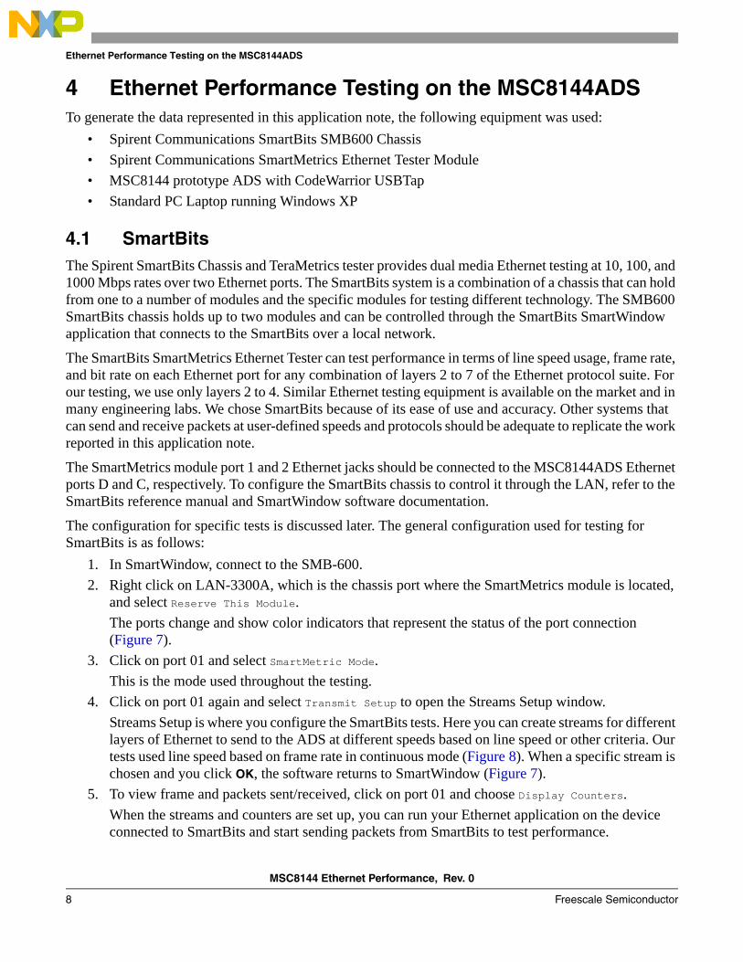
1. In SmartWindow, connect to the SMB-600.2. Right click on LAN-3300A, which is the chassis port where the SmartMetrics module is located,
and select Reserve This Module.The ports change and show color indicators that represent the status of the port connection (Figure 7).
3. Click on port 01 and select SmartMetric Mode.This is the mode used throughout the testing.
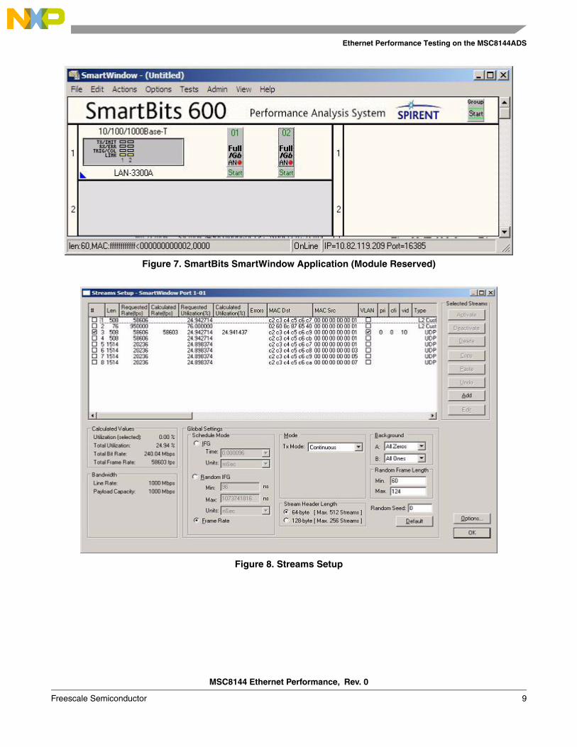
4. Click on port 01 again and select Transmit Setup to open the Streams Setup window.Streams Setup is where you configure the SmartBits tests. Here you can create streams for different layers of Ethernet to send to the ADS at different speeds based on line speed or other criteria. Our tests used line speed based on frame rate in continuous mode (Figure 8). When a specific stream is chosen and you click OK, the software returns to SmartWindow (Figure 7).
5. To view frame and packets sent/received, click on port 01 and choose Display Counters.When the streams and counters are set up, you can run your Ethernet application on the device connected to SmartBits and start sending packets from SmartBits to test performance.
MSC8144 Ethernet Performance, Rev. 0
Freescale Semiconductor 9
Ethernet Performance Testing on the MSC8144ADS
Figure 7. SmartBits SmartWindow Application (Module Reserved)
Figure 8. Streams Setup
MSC8144 Ethernet Performance, Rev. 0
10 Freescale Semiconductor
Ethernet Performance Testing on the MSC8144ADS
4.2 MSC8144ADS BoardThe MSC8144 ADS prototype board used in testing Ethernet performance is equipped with the following items related to Ethernet testing:
• MSC8144 device• MPC8650 PowerQUICC™ device• Marvell quad-port Ethernet PHY• 4-port Ethernet jack• EEPROM for configuration• JTAG debugging connection
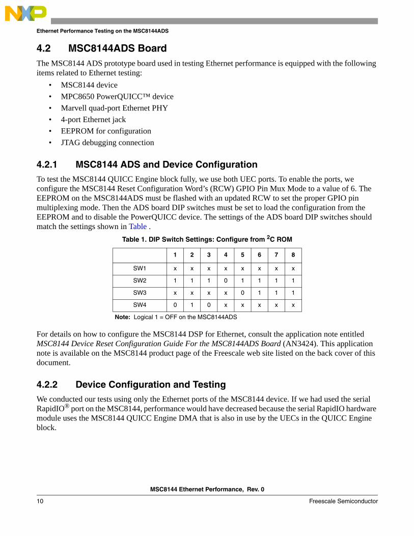
4.2.1 MSC8144 ADS and Device ConfigurationTo test the MSC8144 QUICC Engine block fully, we use both UEC ports. To enable the ports, we configure the MSC8144 Reset Configuration Word’s (RCW) GPIO Pin Mux Mode to a value of 6. The EEPROM on the MSC8144ADS must be flashed with an updated RCW to set the proper GPIO pin multiplexing mode. Then the ADS board DIP switches must be set to load the configuration from the EEPROM and to disable the PowerQUICC device. The settings of the ADS board DIP switches should match the settings shown in Table .
For details on how to configure the MSC8144 DSP for Ethernet, consult the application note entitled MSC8144 Device Reset Configuration Guide For the MSC8144ADS Board (AN3424). This application note is available on the MSC8144 product page of the Freescale web site listed on the back cover of this document.
4.2.2 Device Configuration and TestingWe conducted our tests using only the Ethernet ports of the MSC8144 device. If we had used the serial RapidIO® port on the MSC8144, performance would have decreased because the serial RapidIO hardware module uses the MSC8144 QUICC Engine DMA that is also in use by the UECs in the QUICC Engine block.
Table 1. DIP Switch Settings: Configure from 2C ROM
1 2 3 4 5 6 7 8
SW1 x x x x x x x x
SW2 1 1 1 0 1 1 1 1
SW3 x x x x 0 1 1 1
SW4 0 1 0 x x x x x
Note: Logical 1 = OFF on the MSC8144ADS
MSC8144 Ethernet Performance, Rev. 0
Freescale Semiconductor 11
Performance Testing
4.3 SmartDSP OS Software and DemosThis application note presents both a general Ethernet programming model and an example reference to the SmartDSP OS so that you can replicate the work presented here. Freescale tailors the SmartDSP OS to certain devices, including the MSC8144. Therefore, SmartDSP OS for MSC8144 is provided with the current release version of CodeWarrior (CodeWarrior v3.0). It is a full operating system that includes MSC8144 and MSC8144ADS device and peripheral drivers, interrupt handling and callback routines, timers, task management, multicore communication, profiling, and memory management.
SmartDSP OS is optimized for high performance with a low memory footprint and is the starting-point for the Ethernet testing discussed here. We show a few ways to alter SmartDSP OS to maximize Ethernet performance on the tester and find the theoretical maximum limits of the MSC8144.
The SmartDSP OS install comes with demos for the MSC8144ADS platform to help you get started testing and porting applications to this device. Included in the demos are a Layer 2 (raw Ethernet) loopback demo and a Layer 4 (UDP) echo demo. You can decide where to install the SmartDSP OS. By default, it is installed to the <CodeWarrior Install>\StarCore_Support\SmartDSP directory. The demos are located in \demos under the SmartDSP directory.
5 Performance TestingThis section describes a series of tests, presenting the configurations and the reasoning and rationale for each. Packet size varies from the minimum possible (64 bytes) to 1518 bytes (this is configured in the SmartBits software). The sizes used are: 64, 128, 256, 512, 764, 1020, and 1518 bytes. For smaller packets, both the MSC8144 DSP and the QUICC Engine block must do more work in handling more interrupts and more packets, which fill up the BDs more quickly. As the frame size increases, the load on the processor and the QUICC Engine block decreases.
Testing begins from the top layer down: • Start with UDP testing. Explain the programming model and performance and then give examples
based on the UDP Echo demo.• Test different configurations within UDP L4 and within the software environment.• Move down the protocol suite to raw L2 Ethernet testing.
Performance is expected to increase with each configuration.
5.1 Testing with UDP EchoWe start with UDP echo not only for its simplicity but because we can get an idea of the performance to expect when doing simple read and write accesses to buffers containing Ethernet frames. This knowledge can serve us well when we move all the way down to understanding the raw QUICC Engine throughput in later tests.
The basic register format of the programming model used for the tests is provided as part of the first test. As we proceed, we highlight changes in the register format. The programming model shows the performance-related hardware (register) settings in the MSC8144; it is not an exhaustive guide to programming the MSC8144 for Ethernet. Refer to the reference manual for full programming details.
MSC8144 Ethernet Performance, Rev. 0
12 Freescale Semiconductor
Performance Testing
In the SmartDSP OS demos directory for the MSC8144 (msc814x is the folder name), the folder titled net_demo contains the software for the UDP echo demo on which our examples are based. Because the QUICC Engine UEC is set up to filter in extended parsing mode. Therefore, the SmartDSP OS drivers are set by default to initialize the UEC PCDs to file using Layer 2 MAC addressing. The the upper layers of filtering are performed by interrupt handling software. Because extended mode allows more header parsing, we expect the QUICC Engine to become a bottleneck after some point of optimization. Our goal is to find that point of optimization.
The UDP demo project contains two targets: debug and release. The release target is the optimized version of the demo, and it is used for our tests.
5.1.1 Test 1: One Core at 800 MHz and 1 UECThe MSC8144 is tested with one core running at 800 MHz and one UEC to get a baseline reading and understand the effects of core frequency on Ethernet performance. The MSC8144 UEC receives the packets sent to the MSC8144 from the SmartBits tester. The UEC filters the packet based on MAC address using extended parsing mode. Then, according to the filtering table, it places the packet into the appropriate buffer and interrupts the DSP. The role of the MSC8144 DSP is to read the packet, handle the L4 layer protocol, and then pass the packet to the TX BDs for the UEC to send back to the SmartBits tester.
5.1.1.1 Programming Model
To run the MSC8144 at 800 MHz, the reset configuration word (RCW) registers are configured through I2C ROM to the values listed in Table 2. For a full description of how to program the RCW registers, consult the application note entitled MSC8144 Device Reset Configuration Guide For the MSC8144ADS Board (AN3424).
In this document, we will analyze the software configuration for Ethernet in terms of functional units and use tables containing register information for the final state of the relevant registers. However, will not describe the actual programming order or setup of these registers. The QUICC Engine configuration addresses the following tasks (see Table 3):
• How to manage the UCCs.• Threads and RISC allocation per UCC. The recommended number of threads for a UEC using
Gigabit Ethernet is four for receive and four for transmit.• Interaction between the QUICC Engine block and UCCs.
Using the multi-user RAM available to the QUICC Engine block, space must be initialized for the receive global parameter RAM, transmit global parameter RAM, extended filtering parameters, thread data,
Table 2. General MSC8144 and UEC Interface Registers
Register Address Value
RCWLR EEPROM 0x001F1800 Controls the MSC8144 general clock and PLL settings.
RCWHR EEPROM 0x046C1818 Configured to enable Ethernet I/O
GCR4 0xFFF78030 0x00048000 Configure UEC1 (UCC3) to RGMII and configure pin delay
MSC8144 Ethernet Performance, Rev. 0
Freescale Semiconductor 13
Performance Testing
interrupt coalescing, BD queues, and related data structures. To allocate this space, we use malloc in software and provide base addresses for later use.
The UEC FIFO is programmed to the recommended settings listed in Table 4. These settings do not change (considered static) throughout all of the testing described in this document.
Table 5 lists the interrupt-related parameters.
Table 6 lists the values for the MAC-level configuration.
Table 3. QUICC Engine Configuration
Register Address Value Description
CMXUCR1 0xFEE00410 0x87 QUICC Engine register for clock routing.
GUMR (UCC3) 0xFEE02200 0x0C Configure UEC1 (UCC3) for Ethernet.
GUEMR (UCC3) 0xFEE02290 0x03 Configure UEC1 (UCC3) to fast protocols for Gigabit Ethernet.
Table 4. UCC FIFO Registers
Register Address Value
URFB 0xFEE02220 RX FIFO base address
UCC receive FIFO base address register should be set to the location of the global parameter receive FIFO.
URFS 0xFEE02224 2048 UCC receive FIFO size. In this case, the size is 2048.
URFET 0xFEE02228 1024 UCC receive FIFO emergency treshhold.
URFSET 0xFEE0222A 1536 UCC receive FIFO special emergency threshold.
UTFB 0xFEE0222C TX FIFO base address
UCC transmit FIFO base address register should be set to the location of the global parameter receive FIFO.
UTFS 0xFEE02230 2048 UCC transmit FIFO size. In this case, the size is 2048.
UTFET 0xFEE02234 1024 UCC transmit FIFO emergency treshhold.
UTFTT 0xFEE02238 512 UCC transmit FIFO transmit threshold.
Table 5. Interrupt Registers
Register Address Value
UCCm 0xFEE02214 0xFF000001 UCC mask register enables the mask for interrupts for RX busy, flow control, TX error, back pressure pause, graceful stop, hardware statistics overflow, and magic packet detection. It also enables RX interrupts for the RX queue (channel) 0.
IEN 0xFEE000A0 0x20000000 QUICC Engine block enables UEC1 (UCC3) interrupts.
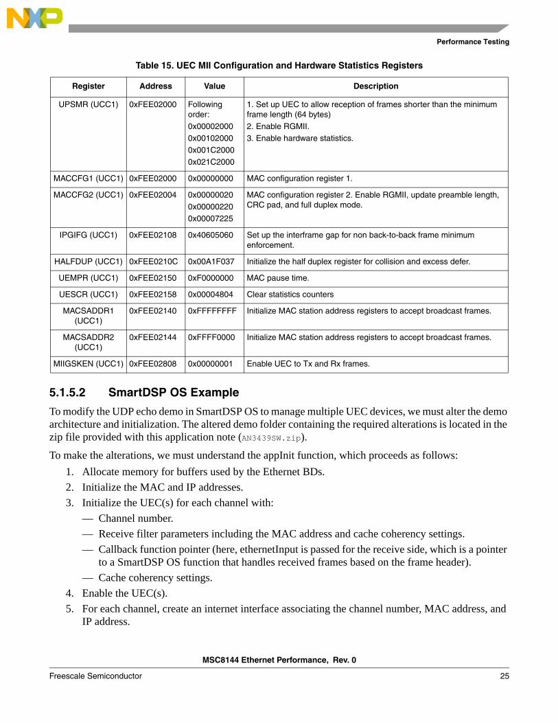
Table 6. UEC MII Configuration and Hardware Statistics Registers
Register Address Value
UPSMR (UCC3) 0xFEE02300 0x021C2000 Sets up the UEC to allow reception of frames shorter than the minimum frame length (64 bytes); enables RGMII and hardware statistics.
MACCFG1 (UCC3) 0xFEE02300 0x00000000 MAC configuration register 1

MSC8144 Ethernet Performance, Rev. 0
14 Freescale Semiconductor
Performance Testing
Global parameter RAM in the QUICC Engine block is available for certain UCC required fields. We must allocate and initialize the RAM sections. Next, we provide their base addresses to the QUICC Engine/UEC in the QUICC Engine scheduler fields (see Table 7).
Table 8 lists the TX global parameter RAM initialization values.
MACCFG2 (UCC3) 0xFEE02304 0x00007225 MAC configuration register 2. Enables RGMII. Also, update preamble length, CRC pad, and full duplex mode.
IPGIFG (UCC3) 0xFEE02308 0x40605060 Set up the interframe gap for non back-to-back frame minimum enforcement.
HALFDUP (UCC3) 0xFEE0230C 0x00A1F037 Initialize the half duplex register for collision and excess defer.
UEMPR (UCC3) 0xFEE02350 0xF0000000 MAC pause time.
UESCR (UCC3) 0xFEE02358 0x00004804 Clear statistics counters.
MACSADDR1 (UCC3)
0xFEE02340 0xFFFFFFFF Initialize MAC station address registers to accept broadcast frames.
MACSADDR2 (UCC3)
0xFEE02344 0xFFFF0000 Initialize MAC station address registers to accept broadcast frames.
MIIGSKEN (UCC3) 0xFEE02A08 0x00000001 Enable UEC to TX and RX frames.
Table 7. UEC Global Parameter RAM Fields
Register Offset Value
REMODER 0x00 0x80001900 Enable extended parsing mode, extended filtering, and two receive queues. Enable RX statistics.
Type or Length 0x20 0x600 Initialize maximum frame length.
MaxFrameLength 0x4C 0x600 Initialize maximum frame length.
MINFLR 0x4E 64 Initialize minimum frame length.
MRBLR 0x46 0x600 Initialize maximum frame length.
MaxD1 0x50 1520 Initialize maximum DMA length.
MaxD2 0x52 1520 Initialize maximum DMA length.
BMR (RSTATE) 0x36 0x10 UEC bus byte ordering (BMR) set to big-endian byte ordering.
L2QT 0x58 0x01234567 L2 QoS Table is set to enable support for eight queues.
L3QT 0x5C 0x00000000 Not used.
Table 8. UEC TX Global Parameter RAM Fields
Register Offset Value
TEMODER 0x00 0x0000E101 Initialize to default values, manage two queues and enable statistics (RMON).
TX Scheduler 0x3C base address Base address to TX scheduler (inserted into following rows).
Table 6. UEC MII Configuration and Hardware Statistics Registers (continued)
Register Address Value

MSC8144 Ethernet Performance, Rev. 0
Freescale Semiconductor 15
Performance Testing
The Ethernet parameters initialization consists of a 56-byte structure with an address assigned by the software programmer. Software must use the QUICC Engine command register (CECR) to enable the QUICC Engine command data register (CECDR) to receive the address to be used for this structure.
The CECDR must be initialized with the Init Ethernet Parameters only after the TX and RX global parameters are initialized. In Table 9, notice that rgfTgfRxGlobal is in bold because this parameter is directly related to the performance of the QUICC Engine block. The recommended number of threads for a UEC using Gigabit Ethernet is four for receive and four for transmit.
• CPUCount0 – 0x0 0 Reset scheduler CPU counts.
• CPUCount1 – 0x2 0
• CPUCount2 – 0x8 0
• CPUCount3 – 0xA 0
• CPUCount4 – 0x10 0
• CPUCount5 – 0x12 0
• CPUCount6 – 0x18 0
• CPUCount7 – 0x1A 0
• MBLInterval – 0x4C 128 Max Burst Length Interval for a 1Gbps burst set to 128
• NORTSRByteTime – 0x50 5 Normalized value of byte type in TSR Units
• FracSiz – 0x52 1 Denominator of the TSRByteTime (radix 2 log)TSRByteTime = NorTSRByteTime / 2^FracSiz
• StrictPriorityQ – 0x54 0xFF All 8 Queues belong to Strict Priority Queue
• TxASAP – 0x55 0xFF Packets are transmitted ASAP from all queues
• ExtraBW – 0x56 0xFF All 8 transmit queues will not consume bandwidth from the budget allowed by the Traffic Shaper
• WeightFactor 0-7 – 0x58 0x000000000x00000000
All 64 bits corresponding to the weight factors for the 8 queues are set to 0 indicating zero wait period following data transmit
TxRmonBasePointer 0x40 address
TSTATE (BMRT) 0x44 0x10000000 Sets transmit to Big Endian Byte Ordering
Table 9. QUICC Engine Scheduler Fields
Register Offset Value
ResInit1 0x00 0x6 Internal variable. Initialize to this value.
ResInit2 0x01 0x30 Internal variable. Initialize to this value.
ResInit3 0x02 0xFF Internal variable. Initialize to this value.
ResInit4 0x03 0x0 Internal variable. Initialize to this value.
ResInit5 0x04 0x400 Internal variable. Initialize to this value.
Table 8. UEC TX Global Parameter RAM Fields (continued)
Register Offset Value

MSC8144 Ethernet Performance, Rev. 0
16 Freescale Semiconductor
Performance Testing
5.1.1.2 Non-SmartDSP OS Programming Model
In addition to configuring the registers as shown in Section 5.1.1.1, “Programming Model,” we must configure the following data structures and registers for our test:
• Initialize the PCD chain for L2 filtering by MAC address (table can include broadcast address and specific individual addresses.
• Initialize the receive buffer descriptors:— Initialize eight (8) RxBDs to the size of the maximum packet to be used (0x600). Set the
external base pointer to memory area for BDs (RxBD parameter table at 0xFEE1B6F0 in this instantiation), and initialize the BD status for the BDs to empty.
— Set the WRAP bit for the last RxBD.• Initialize transmit buffers
— Initialize 32 TxBDs in memory to size 0x600 for transmit usage. Set the status for the BDs to interrupt enabled on completion and the status for the last BD to WRAP.
• Enable UEC1 (UCC3):— Write the offset value to the initialization parameters to the CECDR (at 0xFEE00108). In this
case, the value is 0xA5D8.
ResInit6 0x06 0x00 Internal variable. Initialize to this value.
rgfTgfRxGlobal 0x08 0xBE03 Enable 4 Threads for TX and RX, and enables both RISCs to be used dynamically.
RxGlobalSnum 0x0C 0xE9000003 Snum for Global Task chosen for UEC Receiver
RxSnum1 0x10 0xE800A483 Snum that must always be initialized. Includes Thread1 Parameter Page offset address
RxSnum2 0x14 0xD900A303 Snum and Thread Parameter Page offset address
RxSnum3 0x18 0xD800A103 Snum and Thread Parameter Page offset address
RxSnum4 0x1C 0xC9009F83 Snum and Thread Parameter Page offset address
TxGlobalSnum 0x38 0xBD03(address
Points to TX Global Parameter RAM base (offset). BD03 is the value used by SDOS.
TxSnum1 0x3C 0x2C008C02 Snum and Thread Parameter Page offset address
TxSnum2 0x40 0x25008A82 Snum and Thread Parameter Page offset address
TxSnum3 0x44 0x24008902 Snum and Thread Parameter Page offset address
TxSnum4 0x48 0x1D008702 Snum and Thread Parameter Page offset address
TxSnum5 0x4C 0x1C008582 Snum and Thread Parameter Page offset address
TxSnum6 0x50 0x15008402 Snum and Thread Parameter Page offset address
TxSnum7 0x54 0x14008282 Snum and Thread Parameter Page offset address
TxSnum8 0x58 0x0D008082 Snum and Thread Parameter Page offset address
Table 9. QUICC Engine Scheduler Fields (continued)
Register Offset Value
MSC8144 Ethernet Performance, Rev. 0
Freescale Semiconductor 17
Performance Testing
— Write 0x02410300 to the QUICC Engine CECR register at 0xFEE00100. This is the actual command to the QUICC Engine block that enables UCC3.
— Update the GUMR register value to 0x0000003C to enable RX and TX in the UCCs.— Update the MACCFG1 value to 5 to enable TX and RX in the MAC configuration registers.
• In the tests program, the number of TX and RX BD rings is equal to the number of cores × number of channels.
5.1.1.3 SmartDSP OS Example
The net demo provided with the SmartDSP OS is set up so that the UEC has a MAC address and IP addresses for each active channel per core. By default, SmartDSP OS uses two channels per core. The easiest way to start this demo is to run just one core in the default setup. For a baseline, we run the demo this way, as follows:
1. Open the UDP demo project file (net_demo_core0.mcp). 2. Change the number of cores expected from 4 to 1 (this is set in os_config.h with
OS_NUM_OF_CORES).3. Remove the other executables from the project’s target debugger settings.4. Compile and run the project.
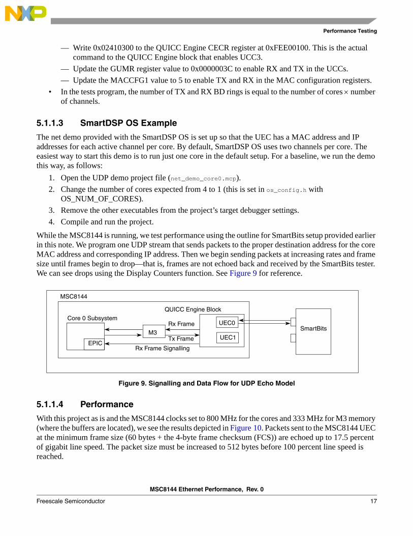
While the MSC8144 is running, we test performance using the outline for SmartBits setup provided earlier in this note. We program one UDP stream that sends packets to the proper destination address for the core MAC address and corresponding IP address. Then we begin sending packets at increasing rates and frame size until frames begin to drop—that is, frames are not echoed back and received by the SmartBits tester. We can see drops using the Display Counters function. See Figure 9 for reference.
Figure 9. Signalling and Data Flow for UDP Echo Model
5.1.1.4 Performance
With this project as is and the MSC8144 clocks set to 800 MHz for the cores and 333 MHz for M3 memory (where the buffers are located), we see the results depicted in Figure 10. Packets sent to the MSC8144 UEC at the minimum frame size (60 bytes + the 4-byte frame checksum (FCS)) are echoed up to 17.5 percent of gigabit line speed. The packet size must be increased to 512 bytes before 100 percent line speed is reached.
M3
Core 0 SubsystemQUICC Engine Block
MSC8144
UEC0
UEC1
SmartBits
EPICRx Frame Signalling
Rx Frame
Tx Frame

MSC8144 Ethernet Performance, Rev. 0
18 Freescale Semiconductor
Performance Testing
Figure 10. UDP Echo@ 800 MHz DSP: Usage Versus Frame Size
To verify that the DSP is not the bottleneck, we can make the following adjustments:• Increase DSP core and memory frequency• Use a shortcut in the UDP send algorithm• Test with four cores• Test with two UECs• Test with buffers located in faster (and slower) memory• Test with the QUICC Engine block using MPC82xx filtering mode
5.1.2 Test 2: Increase DSP Core and Memory FrequencyThe most obvious way to improve core processing performance on the MSC8144 is to increase the frequency. It is expected that increased frequency can also lead to increased Ethernet throughput.
5.1.2.1 Programming Model
Following the method outlined in the application note entitled MSC8144 Device Reset Configuration Guide For the MSC8144ADS Board (AN3424), update the MSC8144 from 800 MHz DSP core frequency and 333 MHz M3 memory frequency to 1 GHz core and 400 MHz M3 memory, and retest Ethernet throughput at the different packet sizes (see Table 10).
0
2 0 0
4 0 0
6 0 0
8 0 0
1 0 0 0
1 2 0 0
6 0 1 2 4 2 5 2 5 0 8 7 6 4 1 0 2 0 1 5 1 4
Mbp
s
8 0 0 M h z

MSC8144 Ethernet Performance, Rev. 0
Freescale Semiconductor 19
Performance Testing
5.1.2.2 Performance
Performance improves slightly, with the minimum packet size (64 bytes including the 4-byte frame checksum) reaching 22 percent of the gigabit Ethernet usage (167 Mbps). The UEC can reach full line speed when the packet size before the packet size reaches 512 bytes, but it is still unable to reach linespeed by 256-byte packet size.
Figure 11. UDP Echo @ 1GHz DSP: Usage Versus Frame Size
5.1.3 Test 3: Improve the UDP Send Function for UDP Echo TestingIn the third test, we seek to increase performance of the SmartDSP OS demo used as an example in this application. You can use a similar strategy performance testing, depending on how the L4 echo application is implemented. In the UDP echo demo, you can see in the main application file, net_demo.c, that frames are echoed back from the callback routine (udpReceiveCallBack) using the udpSendTo function.
This function checks the port and destination address it needs to send the packet to each time (effectively performing a connect back to the sender each time a packet is echoed). For performance testing here, the
Table 10. General MSC8144 and UEC Interface Registers
Register Address Value
RCWLR EEPROM 0x001F1C0A Setting this register controls the MSC8144 general clock and PLL settings to 1 GHz DSP core and 400 MHz M3 memory.
RCWHR EEPROM 0x046C1818 Configured to enable Ethernet I/O.
GCR4 0xFFF78030 0x00048000 Configure UEC1 (UCC3) to RGMII and configure pin delay.
0
200
400
600
800
1000
1200
60 124 252 508 764 1020 1514
Mbp
s
1GHz800Mhz

MSC8144 Ethernet Performance, Rev. 0
20 Freescale Semiconductor
Performance Testing
SmartBits is programmed to send from just one source address and port. This enables switching from using the udpSendTo() function to doing one single connect and then using the udpSend() function, which is already available in SmartDSP OS, for all subsequent echoes. The code to do this is shown Example 1.
Example 1. udpReceiveCallBack Function: Altered for a Single UDP Connection
unsigned int connectonce =0;static os_status udpReceiveCallBack(void* channel_num, os_frame_t* frame){
struct sockaddr_in dest;os_statusstatus;uint32_tchannel = (uint32_t)channel_num;
udpGetSourceAddr(frame, &dest);if (dest.sin_port >= UDP_PORT)
{
if (connectonce == 0)
{
status = udpConnect(test_sockets[channel], &dest);
connectonce++;
}
dest.sin_port = dest.sin_port + 1000;status = udpSend(test_sockets[channel], frame);if(status != OS_SUCCESS)
osFrameFree(sb_frames_pool, frame);
return OS_SUCCESS;
}
return OS_FAIL;// Send ICMP Message
}
We can do udpConnect to multiple destinations based on channel number, as is discussed later.
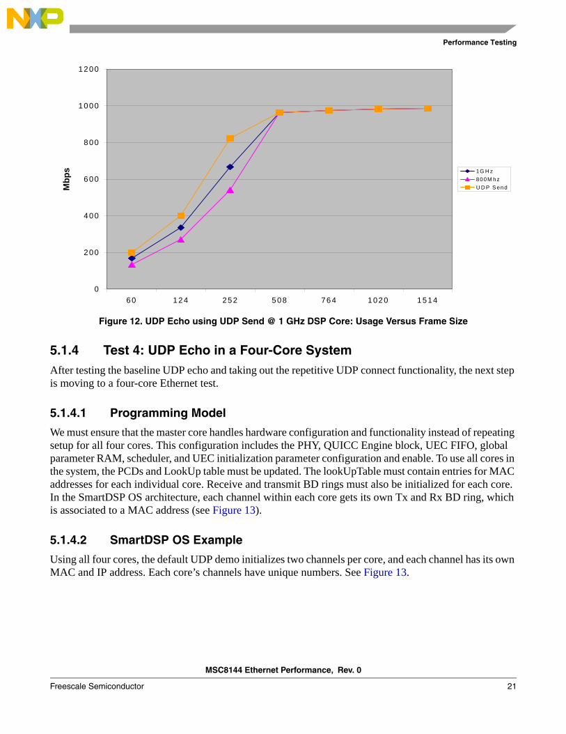
With udpSent(), performance improves once again, to the point that 64-byte packets can be echoed at 26 percent usage of the gigabit line (197 Mbps), and full line speed is reached just after a 256-byte packet length.
MSC8144 Ethernet Performance, Rev. 0
Freescale Semiconductor 21
Performance Testing
Figure 12. UDP Echo using UDP Send @ 1 GHz DSP Core: Usage Versus Frame Size
5.1.4 Test 4: UDP Echo in a Four-Core SystemAfter testing the baseline UDP echo and taking out the repetitive UDP connect functionality, the next step is moving to a four-core Ethernet test.
5.1.4.1 Programming Model
We must ensure that the master core handles hardware configuration and functionality instead of repeating setup for all four cores. This configuration includes the PHY, QUICC Engine block, UEC FIFO, global parameter RAM, scheduler, and UEC initialization parameter configuration and enable. To use all cores in the system, the PCDs and LookUp table must be updated. The lookUpTable must contain entries for MAC addresses for each individual core. Receive and transmit BD rings must also be initialized for each core. In the SmartDSP OS architecture, each channel within each core gets its own Tx and Rx BD ring, which is associated to a MAC address (see Figure 13).
5.1.4.2 SmartDSP OS Example
Using all four cores, the default UDP demo initializes two channels per core, and each channel has its own MAC and IP address. Each core’s channels have unique numbers. See Figure 13.
0
200
400
600
800
1000
1200
60 124 252 508 764 1020 1514
Mbp
s 1G H z800M hzU D P S end

MSC8144 Ethernet Performance, Rev. 0
22 Freescale Semiconductor
Performance Testing
Figure 13. Application Layer Channel Usage for Single UEC Model
Altering the SmartDSP OS project is a simple two-step process:1. Change OS_NUM_OF_CORES to 4 in os_config.h.2. Add net_core1.mcp to net_core3.mcp back to the project’s target settings → debugger → other
executables panel.
We recompile and debug the project, ensuring that all cores are running the “release” version of the demo. To test this with SmartBits, we add three more streams. There is one stream for each core with its corresponding MAC and IP address in addition to a UDP port greater than 10000. There are six more streams for testing both channels available. At this point, we can run the test, pinging all cores simultaneously. Figure 14 shows the general system model.
Figure 14. UDP Echo 4 Core with Single UEC Model
Channel 0
Channel 1
Channel 2
Channel 3
Channel 4
Channel 5
Channel 6
Channel 7
UEC0UEC
of Channels
Visibility
ApplicationView of Channels
Channel 0
Channel 1
Channel 2
Channel 3
Channel 4
Channel 5
Channel 6
Channel 7
...
Core 0
Core 1
Core 2
Core 3
M3
Core 0 Subsystem
QUICC
MSC8144
UEC1
SmartBits
EPICRx Frame Signalling
Rx Frame
Tx Frame
M3
Core 1 Subsystem
EPICRx Frame Signalling
Rx Frame
Tx Frame
M3
Core 2 Subsystem
EPICRx Frame Signalling
Rx Frame
Tx Frame
M3
Core 3 Subsystem
EPICRx Frame Signalling
Rx Frame
Tx Frame
UEC0
EngineBlock
MSC8144 Ethernet Performance, Rev. 0
Freescale Semiconductor 23
Performance Testing
5.1.4.3 Performance
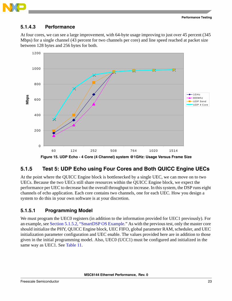
At four cores, we can see a large improvement, with 64-byte usage improving to just over 45 percent (345 Mbps) for a single channel (43 percent for two channels per core) and line speed reached at packet size between 128 bytes and 256 bytes for both.
Figure 15. UDP Echo - 4 Core (4 Channel) system @1GHz: Usage Versus Frame Size
5.1.5 Test 5: UDP Echo using Four Cores and Both QUICC Engine UECsAt the point where the QUICC Engine block is bottlenecked by a single UEC, we can move on to two UECs. Because the two UECs still share resources within the QUICC Engine block, we expect the performance per UEC to decrease but the overall throughput to increase. In this system, the DSP runs eight channels of echo application. Each core contains two channels, one for each UEC. How you design a system to do this in your own software is at your discretion.
5.1.5.1 Programming Model
We must program the UEC0 registers (in addition to the information provided for UEC1 previously). For an example, see Section 5.1.5.2, “SmartDSP OS Example.” As with the previous test, only the master core should initialize the PHY, QUICC Engine block, UEC FIFO, global parameter RAM, scheduler, and UEC initialization parameter configuration and UEC enable. The values provided here are in addition to those given in the initial programming model. Also, UEC0 (UCC1) must be configured and initialized in the same way as UEC1. See Table 11.
0
200
400
600
800
1000
1200
60 124 252 508 764 1020 1514
Mbp
s 1G H z800M hzU D P SendU D P 4 C ore

MSC8144 Ethernet Performance, Rev. 0
24 Freescale Semiconductor
Performance Testing
The PHY master for MDIO and MDC remains UEC1. The UEC0 PHY interface must be configured as well to connect to the ADS Vitesse Gigabit Ethernet switch at Gigabit Ethernet speed. Because this interface is configured to Gigabit Ethernet and not altered, programming the Vitesse is not discussed in this application note. Table 12 through Table 14 list the necessary register values. UEC0 also has its own global Rx and Tx parameter RAM, initialized with the same values as UEC1. These values are provided to the UEC through the scheduler structure as they are for UEC1.
Table 11. General MSC8144 and UEC Interface Registers
Register Address Value
GCR4 0xFFF78030 0x00048120 Configure UEC1 and UEC0 to RGMII and configure pin delay.
Table 12. QUICC Engine Configuration
Register Address Value Description
CMXUCR1 0xFEE00410 0x00650087 QUICC Engine register for clock routing of UCC1 and UCC3.
GUMR (UCC1) 0xFEE02000 0x0C Configure UEC1 (UCC3) for Ethernet.
GUEMR (UCC1) 0xFEE02090 0x13 Configure UEC1 (UCC3) to fast protocols for Gigabit Ethernet.
Table 13. UCC FIFO Registers
Register Address Value
URFB 0xFEE02020 RX FIFO base address
UCC receive FIFO base address register should be set to the location of the global parameter receive FIFO.
URFS 0xFEE02024 2048 UCC receive FIFO size. In this case, the size is 2048.
URFET 0xFEE02028 1024 UCC receive FIFO emergency treshhold.
URFSET 0xFEE0202A 1536 UCC receive FIFO special emergency threshold.
UTFB 0xFEE0202C TX FIFO base address
UCC transmit FIFO base address register should be set to the location of the global parameter receive FIFO.
UTFS 0xFEE02030 2048 UCC transmit FIFO size. In this case, the size is 2048.
UTFET 0xFEE02034 1024 UCC transmit FIFO emergency treshhold.
UTFTT 0xFEE02038 512 UCC transmit FIFO transmit threshold.
Table 14. Interrupt Registers
Register Address Value Description
UER 0xFEE02010 0xFFFFFFFF Clear UEC1 (UCC3) events.
UCCM 0xFEE02014 0xFF000000
0xFF000001
UCC mask register enables mask for interrupts for Rx busy, flow control, Tx error, back pressure pause, graceful stop, hardware statistics overflow, and magic packet detection. Enable Rx interrupts for Rx queue (channel) 0.
IEN 0xFEE000A0 0xA0000000 QUICC Engine block enables UEC1 (UCC3) and UEC0 (UCC1) interrupts.
MSC8144 Ethernet Performance, Rev. 0
Freescale Semiconductor 25
Performance Testing
5.1.5.2 SmartDSP OS Example
To modify the UDP echo demo in SmartDSP OS to manage multiple UEC devices, we must alter the demo architecture and initialization. The altered demo folder containing the required alterations is located in the zip file provided with this application note (AN3439SW.zip).
To make the alterations, we must understand the appInit function, which proceeds as follows:1. Allocate memory for buffers used by the Ethernet BDs.2. Initialize the MAC and IP addresses.3. Initialize the UEC(s) for each channel with:
— Channel number.— Receive filter parameters including the MAC address and cache coherency settings.— Callback function pointer (here, ethernetInput is passed for the receive side, which is a pointer
to a SmartDSP OS function that handles received frames based on the frame header). — Cache coherency settings.
4. Enable the UEC(s).5. For each channel, create an internet interface associating the channel number, MAC address, and
IP address.
Table 15. UEC MII Configuration and Hardware Statistics Registers
Register Address Value Description
UPSMR (UCC1) 0xFEE02000 Following order:
0x00002000
0x001020000x001C2000
0x021C2000
1. Set up UEC to allow reception of frames shorter than the minimum frame length (64 bytes)
2. Enable RGMII.
3. Enable hardware statistics.
MACCFG1 (UCC1) 0xFEE02000 0x00000000 MAC configuration register 1.
MACCFG2 (UCC1) 0xFEE02004 0x00000020
0x000002200x00007225
MAC configuration register 2. Enable RGMII, update preamble length, CRC pad, and full duplex mode.
IPGIFG (UCC1) 0xFEE02108 0x40605060 Set up the interframe gap for non back-to-back frame minimum enforcement.
HALFDUP (UCC1) 0xFEE0210C 0x00A1F037 Initialize the half duplex register for collision and excess defer.
UEMPR (UCC1) 0xFEE02150 0xF0000000 MAC pause time.
UESCR (UCC1) 0xFEE02158 0x00004804 Clear statistics counters
MACSADDR1 (UCC1)
0xFEE02140 0xFFFFFFFF Initialize MAC station address registers to accept broadcast frames.
MACSADDR2 (UCC1)
0xFEE02144 0xFFFF0000 Initialize MAC station address registers to accept broadcast frames.
MIIGSKEN (UCC1) 0xFEE02808 0x00000001 Enable UEC to Tx and Rx frames.

MSC8144 Ethernet Performance, Rev. 0
26 Freescale Semiconductor
Performance Testing
The demo currently sets up a specific number of channels per UEC, assuming one UEC per core. Therefore, the code must be changed to manage channels per UECs per core. We assigned the even channels to UEC0 and the odd channels to UEC1 at the application level. However, at the driver (hardware) level of SmartDSP OS, both UECs would receive the same settings. For example, UEC1 can be set up to filter a UDP channel to core 0 so that the UEC sees this as channel 0. However, the application layer handles this as channel 1 (and the application uses its version of channel numbers as one way to differentiate between UECs). Figure 16 illustrates this idea.
Figure 16. Application Layer Channel Usage for Dual UEC Model
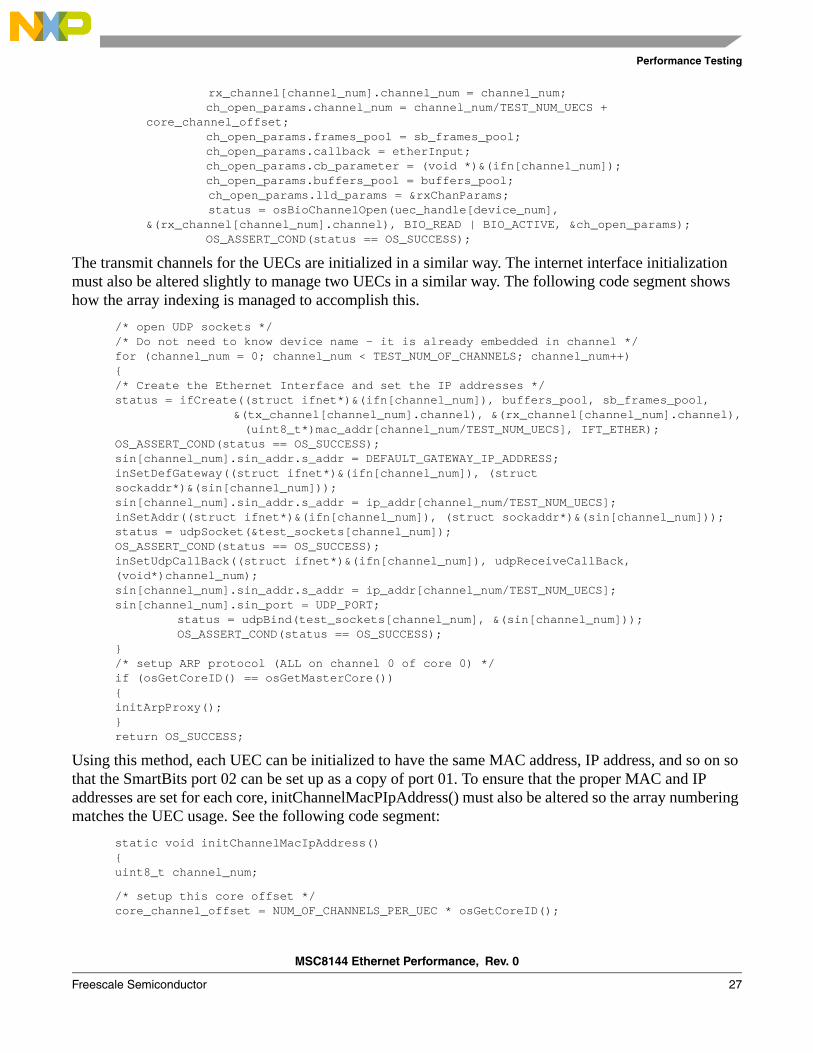
The following code segment shows how the UECs should be initialized in the altered appInit() function. Note that some variables need to be defined, such as uec_handle, which can be defined similarly to uec_handle1 from the original project, but as an array: “uec_handle[number_of_uecs]“
/* open the UEC device, with default parameters */dev_open_params.common_pool = NULL;dev_open_params.lld_params = NULL;for(device_num = 0; device_num < TEST_NUM_UECS; device_num++){
connectonce[device_num] = 0;if(device_num == 0){uec_handle[0] = osBioDeviceOpen(UEC0_DEVICE_NAME, &dev_open_params);
OS_ASSERT_COND(uec_handle[0] != NULL);
else if (device_num == 1){uec_handle[1] = osBioDeviceOpen(UEC1_DEVICE_NAME, &dev_open_params);OS_ASSERT_COND(uec_handle[1] != NULL); }
else OS_ASSERT;/* open channels *//* We put first channel to UEC0, second to UEC1 etc. */for (channel_num = device_num; channel_num < TEST_NUM_OF_CHANNELS; channel_num
+= TEST_NUM_UECS){ /* open the receive channel */
rxChanParams.bd_ring_len = 8; rxChanParams.addr_high32 = mac_addr[channel_num/TEST_NUM_UECS][0]; rxChanParams.addr_low16 = mac_addr[channel_num/TEST_NUM_UECS][1] >> 16;
rxChanParams.coherency_en = DCACHE_ENABLE;
rxChanParams.interrupt_en = TRUE;rx_channel[channel_num].device_num = device_num;
Channel 0
Channel 1
Channel 2
Channel 3
Channel 0
Channel 1
Channel 2
Channel 3
UEC0
UEC1
UEC Low-
of Channels
View
Application
Layer View
Of Channels
Channel 0
Channel 1
Channel 2
Channel 3
Channel 4
Channel 5
Channel 6
Channel 7
...
Level Driver
MSC8144 Ethernet Performance, Rev. 0
Freescale Semiconductor 27
Performance Testing
rx_channel[channel_num].channel_num = channel_num; ch_open_params.channel_num = channel_num/TEST_NUM_UECS +
core_channel_offset; ch_open_params.frames_pool = sb_frames_pool; ch_open_params.callback = etherInput; ch_open_params.cb_parameter = (void *)&(ifn[channel_num]); ch_open_params.buffers_pool = buffers_pool;
ch_open_params.lld_params = &rxChanParams;status = osBioChannelOpen(uec_handle[device_num],
&(rx_channel[channel_num].channel), BIO_READ | BIO_ACTIVE, &ch_open_params); OS_ASSERT_COND(status == OS_SUCCESS);
The transmit channels for the UECs are initialized in a similar way. The internet interface initialization must also be altered slightly to manage two UECs in a similar way. The following code segment shows how the array indexing is managed to accomplish this.
/* open UDP sockets *//* Do not need to know device name - it is already embedded in channel */for (channel_num = 0; channel_num < TEST_NUM_OF_CHANNELS; channel_num++){/* Create the Ethernet Interface and set the IP addresses */status = ifCreate((struct ifnet*)&(ifn[channel_num]), buffers_pool, sb_frames_pool, &(tx_channel[channel_num].channel), &(rx_channel[channel_num].channel), (uint8_t*)mac_addr[channel_num/TEST_NUM_UECS], IFT_ETHER);OS_ASSERT_COND(status == OS_SUCCESS);sin[channel_num].sin_addr.s_addr = DEFAULT_GATEWAY_IP_ADDRESS;inSetDefGateway((struct ifnet*)&(ifn[channel_num]), (struct sockaddr*)&(sin[channel_num]));sin[channel_num].sin_addr.s_addr = ip_addr[channel_num/TEST_NUM_UECS];inSetAddr((struct ifnet*)&(ifn[channel_num]), (struct sockaddr*)&(sin[channel_num]));status = udpSocket(&test_sockets[channel_num]);OS_ASSERT_COND(status == OS_SUCCESS);inSetUdpCallBack((struct ifnet*)&(ifn[channel_num]), udpReceiveCallBack, (void*)channel_num);sin[channel_num].sin_addr.s_addr = ip_addr[channel_num/TEST_NUM_UECS];sin[channel_num].sin_port = UDP_PORT;
status = udpBind(test_sockets[channel_num], &(sin[channel_num]));OS_ASSERT_COND(status == OS_SUCCESS);
}/* setup ARP protocol (ALL on channel 0 of core 0) */if (osGetCoreID() == osGetMasterCore()){initArpProxy();}return OS_SUCCESS;
Using this method, each UEC can be initialized to have the same MAC address, IP address, and so on so that the SmartBits port 02 can be set up as a copy of port 01. To ensure that the proper MAC and IP addresses are set for each core, initChannelMacPIpAddress() must also be altered so the array numbering matches the UEC usage. See the following code segment:
static void initChannelMacIpAddress(){uint8_t channel_num;
/* setup this core offset */core_channel_offset = NUM_OF_CHANNELS_PER_UEC * osGetCoreID();
MSC8144 Ethernet Performance, Rev. 0
28 Freescale Semiconductor
Performance Testing
/* setup mac/ip address for each channel there being 2 channels for each core*/for (channel_num = 0; channel_num < TEST_NUM_OF_CHANNELS; channel_num++)
{
/* setup channel mac address */mac_addr[channel_num][0] = BASE_MAC_ADDR_HIGH32;
mac_addr[channel_num][1] = (BASE_MAC_ADDR_LOW16 + channel_num + core_channel_offset) << 16;
/* setup channel IP address */ip_addr[channel_num] = BASE_IP_ADDRESS + channel_num + core_channel_offset;
}
Additionally, because the way the UECs view the channels has changed but the number of total channels has not, the SmartDSP OS driver must be made aware of this before running appInit(). Otherwise, it fails checks to verify that the number of channels for each UEC matches up with the application level. To manage this situation, we must change msc814x_config.c basic initialization parameters about each UEC (including MII/RMII/RGMII, number of queues, data size, and so on). For dual UECs, the number of BD rings must be changed as follows:
OS_NUM_OF_CORES*NUM_OF_CHANNELS_PER_UEC,/* Number of Tx BD rings */OS_NUM_OF_CORES*NUM_OF_CHANNELS_PER_UEC,/* Number of Rx BD rings */
Where NUM_OF_CHANNELS_PER_UEC is set in app_config.h as follows:#define NUM_OF_CHANNELS_PER_UEC (TEST_NUM_OF_CHANNELS/TEST_NUM_UECS)
Note that this channel’s per UEC pre-processor definition is used in the initChannelMacIpAddress function to set the core channel offset variable. This variable is changed according to the number of channels of each UEC. Refer to Figure 14. To keep using the udpSend() function in the callback routine, the callback routine can be changed to connect once based on just port number. By doing this and then setting a specific UDP port number for all the streams of each SmartBits port to use, udpConnect can still be managed and the overhead of the continuous connects done in the udpSendTo() function can be avoided. See the following code segment for an example.
static os_status udpReceiveCallBack(void* channel_num, os_frame_t* frame)
{
struct sockaddr_in dest;os_statusstatus;uint32_tchannel = (uint32_t)channel_num;
udpGetSourceAddr(frame, &dest);
if (dest.sin_port == 10001){
if (connectonce[0] == 0)
{status =
udpConnect(test_sockets[channel], &dest);
connectonce[0]++;
}
dest.sin_port = dest.sin_port + 1000;status = udpSend(test_sockets[channel], frame);if(status != OS_SUCCESS)
osFrameFree(sb_frames_pool, frame);
return OS_SUCCESS;
MSC8144 Ethernet Performance, Rev. 0
Freescale Semiconductor 29
Performance Testing
}
else if (dest.sin_port == 10002)
{
if (connectonce[1] == 0)
{
status = udpConnect(test_sockets[channel], &dest);
connectonce[1]++;
}
dest.sin_port = dest.sin_port + 1000;status = udpSend(test_sockets[channel], frame);if(status != OS_SUCCESS)
osFrameFree(sb_frames_pool, frame);
return OS_SUCCESS;
}
return OS_FAIL;// Send ICMP Message
}
5.1.5.3 SmartBits Setup
In the SmartWindow, click and copy port one (and select to copy all). Paste this to port 2. To associate each UEC with a SmartBits port, the UDP streams in each SmartBits port must be assigned a UDP port. For Reference: This is already provided in the zip that comes with the application note - see the smartbits files for UDP Echo for 2 UECs. As in the udpReceiveCallBack function, we assign all streams in SmartBits Port 01 to 10002 and all streams in SmartBits Port 02 to 10001. Now we can run the test using all four cores and two UECs of the MSC8144. Figure 17 illustrates the testing model.

MSC8144 Ethernet Performance, Rev. 0
30 Freescale Semiconductor
Performance Testing
Figure 17. UDP Echo 4 Core and 2 UEC Model
5.1.5.4 Performance
As expected, the performance per UEC decreased because previously unshared QUICC Engine resources are now shared by 2 UECs. However, overall performance did improve. Now 64-byte packets are echoed at just over 30 percent of gigabit line speed (231 Mbps) per UEC for a combined total of 462 Mbps QUICC Engine Ethernet throughput. Full Ethernet usage is reached before the 512-byte packet size is reached, allowing the QUICC Engine block to achieve full 2 Gbps Ethernet throughput.
Core 0 Subsystem
QUICC
MSC8144
UEC1
SmartBits
EPICRx Frame Signalling
Rx Frame
Tx Frame
M3
Core 1 Subsystem
EPICRx Frame Signalling
Rx Frame
Tx Frame
M3
Core 2 Subsystem
EPICRx Frame Signalling
Rx Frame
Tx Frame
M3
Core 3 Subsystem
EPICRx Frame Signalling
Rx Frame
Tx Frame
UEC0
M3
EngineBlock

MSC8144 Ethernet Performance, Rev. 0
Freescale Semiconductor 31
Performance Testing
Figure 18. UDP Echo: 4 Cores and 2 UECs, Dual GbE Usage Versus Frame Size
5.1.6 Test 6: Buffers in M2 and DDR MemoryBy default, the SmartDSP OS examples use M3 memory to store the transmit and receive buffer pool used by the RxBDs and TxBDs. As Figure 3 shows, there are three main memories readily available to the MSC8144 on the ADS board: M2, M3, and DDR:
• M2 memory is connected through four 128-bit ports at the class speed (400 MHz)• M3 memory is connected to the 400 MHz class through a single 128-bit 400 MHz (max) port. • The DDR memory controller connected to the CLASS is limited in bandwidth by its connection
external to the device. The class interface speed to the DDR controller is 400 MHz. At this rate, the external MCK signal to the 32-bit DDR devices on the ADS is 200 MHz (providing an effective bandwidth of 400 MHz at 32 bits).
5.1.6.1 Programming Model
The general programming model for this test is very similar to the tasks to be done in SmartDSP OS—to the point that you should simply refer to the SmartDSP OS example for this section of the application note. Note that the reduced size of M2 memory can make it impossible to test packet sizes fully all the way up to 0x600 bytes. This is a restriction in SmartDSP OS.
0
500
1000
1500
2000
2500
60 124 252 508 764 1020 1514
Mbp
s
1G H z800M hzU D P SendU D P 4 C ore4core 2uec
MSC8144 Ethernet Performance, Rev. 0
32 Freescale Semiconductor
Performance Testing
5.1.6.2 SmartDSP OS Example
To test with buffers in different locations, make the following basic modifications to the code: 1. Create a pragma at the variable definition that specifies to CodeWarrior the group in which to store
the variable.2. Add the segment name used in the pragma to the linker command file.
This name is used to file the segment with the rest of the segments associated with that memory.3. For smaller memories such as M2, reduce the total size of the buffer pool so that the segment can
still fit.
Now we must update the project for buffer stores in M2 memory. In the definition for the data buffers, we change the pragma to reflect M2 memory. We change data_buffers.c from:
#pragma data_seg_name ".local_data_m3"
to #pragma data_seg_name ".local_data_m2”
Now we change the linker command file local_map_link.lcf in the net_multicore/linker_files/ directory. The .concatenate instruction tells the linker to combine (concatenate) a number of segments into just one. For local_map_link, many segments are placed into the segment local_data, so the next step is to add the .local_data_m2 segment as well:
; Local Memory; Put all the local memory segments to "local_data"
.concatenate local_data,".local_data_m2",".oskernel_local_data",".data", "ramsp_0", ".rom",".exception_index",".bss", ".oskernel_bss", ".ramsp_0",".init_table", ".rom_init" ,".bsstab",".rom_init_tables",".staticinit",".att_mmu"
Finally, we reduce the buffer pool size in two ways. In app_config.h, reduce TEST_DATA_SIZE from 0x600 to 0x100 to limit the packet size in the test to a maximum of 256 bytes. Also, we reduce the TEST_NUM_OF_BUFS to TEST_NUM_OF_CHANNELS * (8 + 8).
5.1.6.3 Performance
When we compile and rerun the tests, we find that we get the same performance when the buffers are stored in M2 memory as when they are stored in M3 memory. Repeating the test for DDR (but skipping the .concatenate step) yields the same results as well. We explain these results as follows:
• Because the only application running on the MSC8144 is for the Ethernet echo, the possibility for contention during accesses to the single port of M3 or DDR memory is much lower.
• Also, caches are in use, which greatly reduces the number of times the core goes to actual memory to complete any task other than sending frames to and from the UEC.
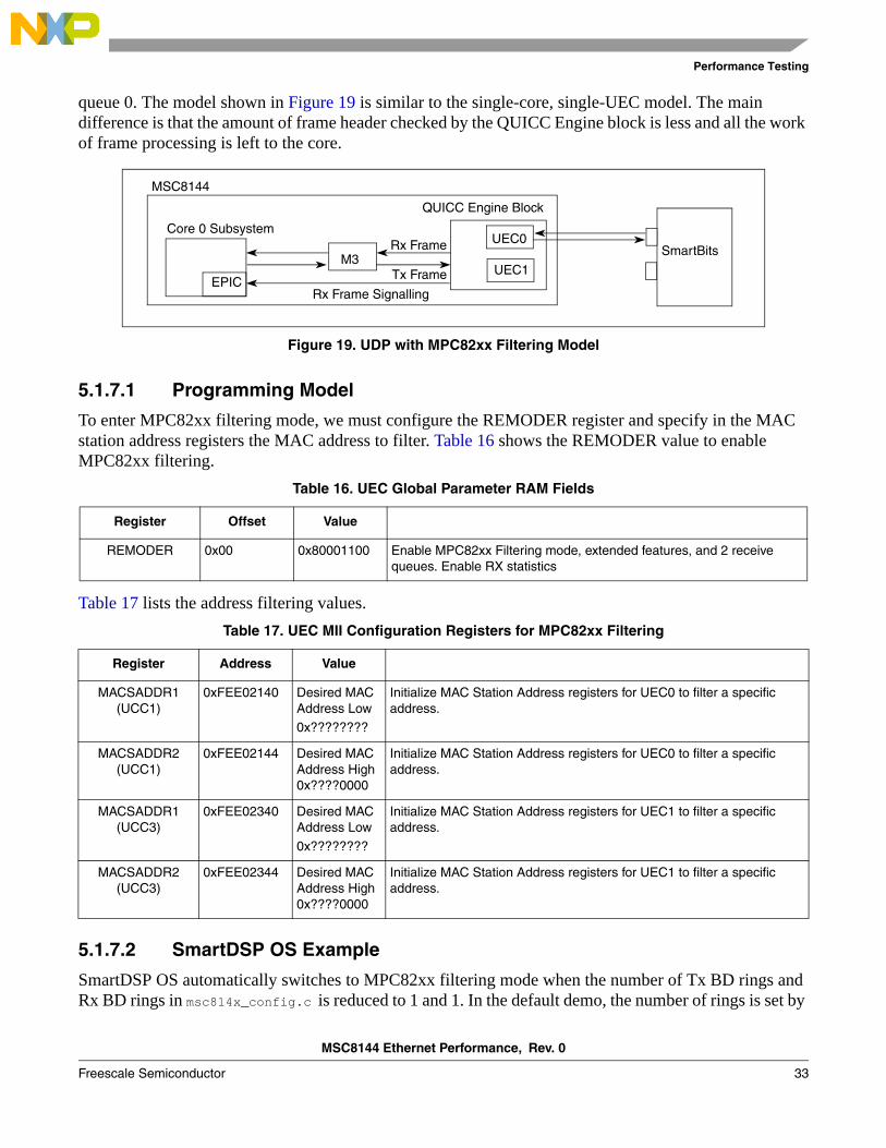
5.1.7 Test 7: QUICC Engine Block Operating in MPC82xx Filtering ModeSwitching to MPC82xx compatible filtering mode from extended parsing mode, as explained in Section 3, “Ethernet Controller (UEC) Frame Filtering,” only filters, accepts, or discards frames based on a single MAC address (unless extended features are enabled). The UEC sends accepted frames exclusively to
MSC8144 Ethernet Performance, Rev. 0
Freescale Semiconductor 33
Performance Testing
queue 0. The model shown in Figure 19 is similar to the single-core, single-UEC model. The main difference is that the amount of frame header checked by the QUICC Engine block is less and all the work of frame processing is left to the core.
Figure 19. UDP with MPC82xx Filtering Model
5.1.7.1 Programming Model
To enter MPC82xx filtering mode, we must configure the REMODER register and specify in the MAC station address registers the MAC address to filter. Table 16 shows the REMODER value to enable MPC82xx filtering.
Table 17 lists the address filtering values.
5.1.7.2 SmartDSP OS Example
SmartDSP OS automatically switches to MPC82xx filtering mode when the number of Tx BD rings and Rx BD rings in msc814x_config.c is reduced to 1 and 1. In the default demo, the number of rings is set by
Table 16. UEC Global Parameter RAM Fields
Register Offset Value
REMODER 0x00 0x80001100 Enable MPC82xx Filtering mode, extended features, and 2 receive queues. Enable RX statistics
Table 17. UEC MII Configuration Registers for MPC82xx Filtering
Register Address Value
MACSADDR1 (UCC1)
0xFEE02140 Desired MAC Address Low0x????????
Initialize MAC Station Address registers for UEC0 to filter a specific address.
MACSADDR2 (UCC1)
0xFEE02144 Desired MAC Address High 0x????0000
Initialize MAC Station Address registers for UEC0 to filter a specific address.
MACSADDR1 (UCC3)
0xFEE02340 Desired MAC Address Low
0x????????
Initialize MAC Station Address registers for UEC1 to filter a specific address.
MACSADDR2 (UCC3)
0xFEE02344 Desired MAC Address High 0x????0000
Initialize MAC Station Address registers for UEC1 to filter a specific address.
M3
Core 0 Subsystem
QUICC Engine Block
MSC8144
UEC0
UEC1
SmartBits
EPICRx Frame Signalling
Rx Frame
Tx Frame
MSC8144 Ethernet Performance, Rev. 0
34 Freescale Semiconductor
Performance Testing
the number of cores multiplied by the number of channels. However, when enabling four-core, dual-UEC testing, we altered this default so that the number of Tx BD rings passed to the low-level SmartDSP OS drivers reflects the number per UEC. Therefore, the only modification needed to test MPC82xx filtering mode is to change the number of cores in os_config.h to 1.
5.1.7.3 Performance
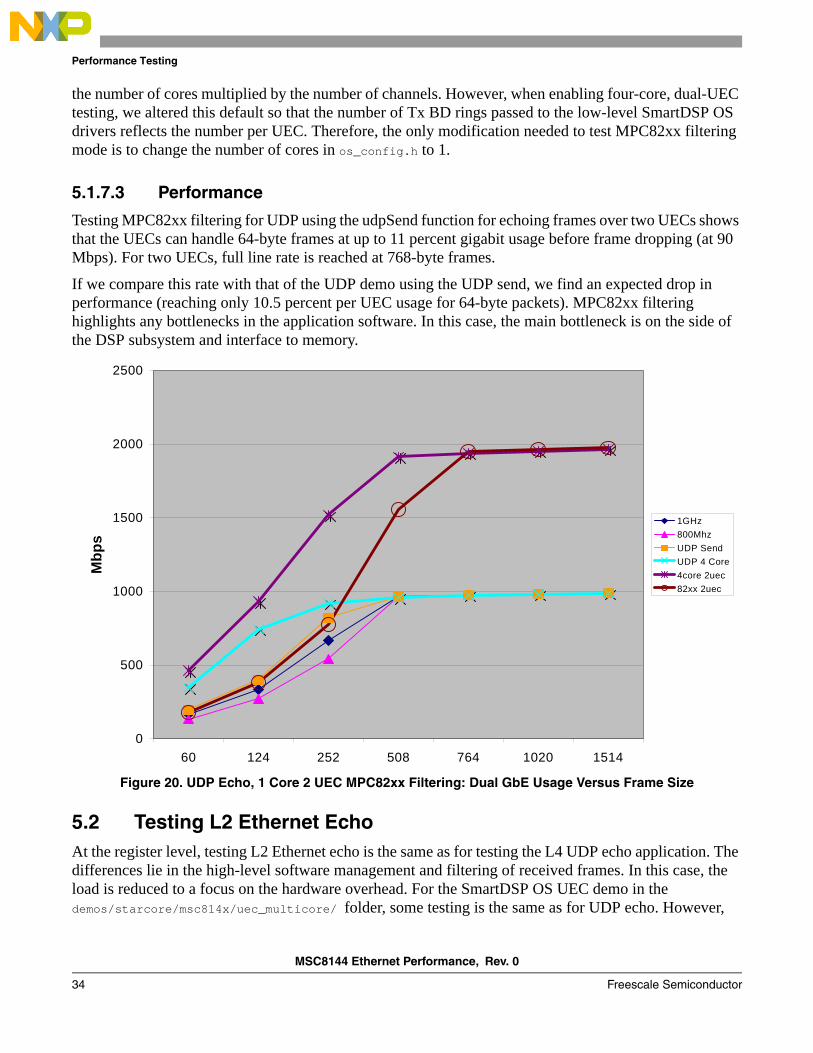
Testing MPC82xx filtering for UDP using the udpSend function for echoing frames over two UECs shows that the UECs can handle 64-byte frames at up to 11 percent gigabit usage before frame dropping (at 90 Mbps). For two UECs, full line rate is reached at 768-byte frames.
If we compare this rate with that of the UDP demo using the UDP send, we find an expected drop in performance (reaching only 10.5 percent per UEC usage for 64-byte packets). MPC82xx filtering highlights any bottlenecks in the application software. In this case, the main bottleneck is on the side of the DSP subsystem and interface to memory.
Figure 20. UDP Echo, 1 Core 2 UEC MPC82xx Filtering: Dual GbE Usage Versus Frame Size
5.2 Testing L2 Ethernet EchoAt the register level, testing L2 Ethernet echo is the same as for testing the L4 UDP echo application. The differences lie in the high-level software management and filtering of received frames. In this case, the load is reduced to a focus on the hardware overhead. For the SmartDSP OS UEC demo in the demos/starcore/msc814x/uec_multicore/ folder, some testing is the same as for UDP echo. However,
0
500
1000
1500
2000
2500
60 124 252 508 764 1020 1514
Mbp
s
1GHz800MhzUDP SendUDP 4 Core4core 2uec82xx 2uec
MSC8144 Ethernet Performance, Rev. 0
Freescale Semiconductor 35
Performance Testing
because UEC involves only filtering for MAC addressing, some experiments from the UDP testing are not used. Testing begins with the UEC demo, which sets up one UEC to loopback frames and filter received frames based on MAC layer filtering in extended parsing mode.
5.2.1 Test 8: UEC L2 Echo with Single Core, Single UECThe test described here gives a baseline for UEC echo testing and also something to compare to the UDP single-core, single-UEC echo application.
5.2.1.1 Programming Model
The register model remains the same as for the single-core, single-UEC L4 UDP echo test described at the start of this application note. You can handle higher levels of abstraction in your operating system/ application at your discretion. The SmartDSP OS example is one option to follow.
5.2.1.2 SmartDSP OS Example
To switch the UEC demo to echo frames (1 core), proceed as follows:1. At the project level:
a) Select the External Loopback target.b) Target settings → Debugging → Other executables (uncheck these).
2. In os_config.h:a) Change OS_NUM_OF_CORES to 1.b) Change MSC814X_UEC0 to ON (to be used later for dual UEC testing).
3. In uec_demo.c: main(), change the loopback variable to match this one:bsp_marvell_external_loopback = FALSE;
4. In uec_demo.c: appInit(), for a single core and single UEC, nothing needs to be changed.5. In uec_demo.c: appBackground():
a) Delete everything after the first while loop.b) Add an infinite loop at the end of appBackground().
6. In uec_demo.c: appBackground(): • Delete everything after data is assigned.• Add the following line at the end of the function to transmit the received frame:
while (osBioChannelTx(&(tx_channel[channel_num].channel), frame) != OS_SUCCESS) ;
5.2.1.3 SmartBits Testing
For UEC loopback, create a standard L2 stream with the destination MAC address matching the UEC projects MAC receive addresses.
MSC8144 Ethernet Performance, Rev. 0
36 Freescale Semiconductor
Performance Testing
5.2.1.4 Performance
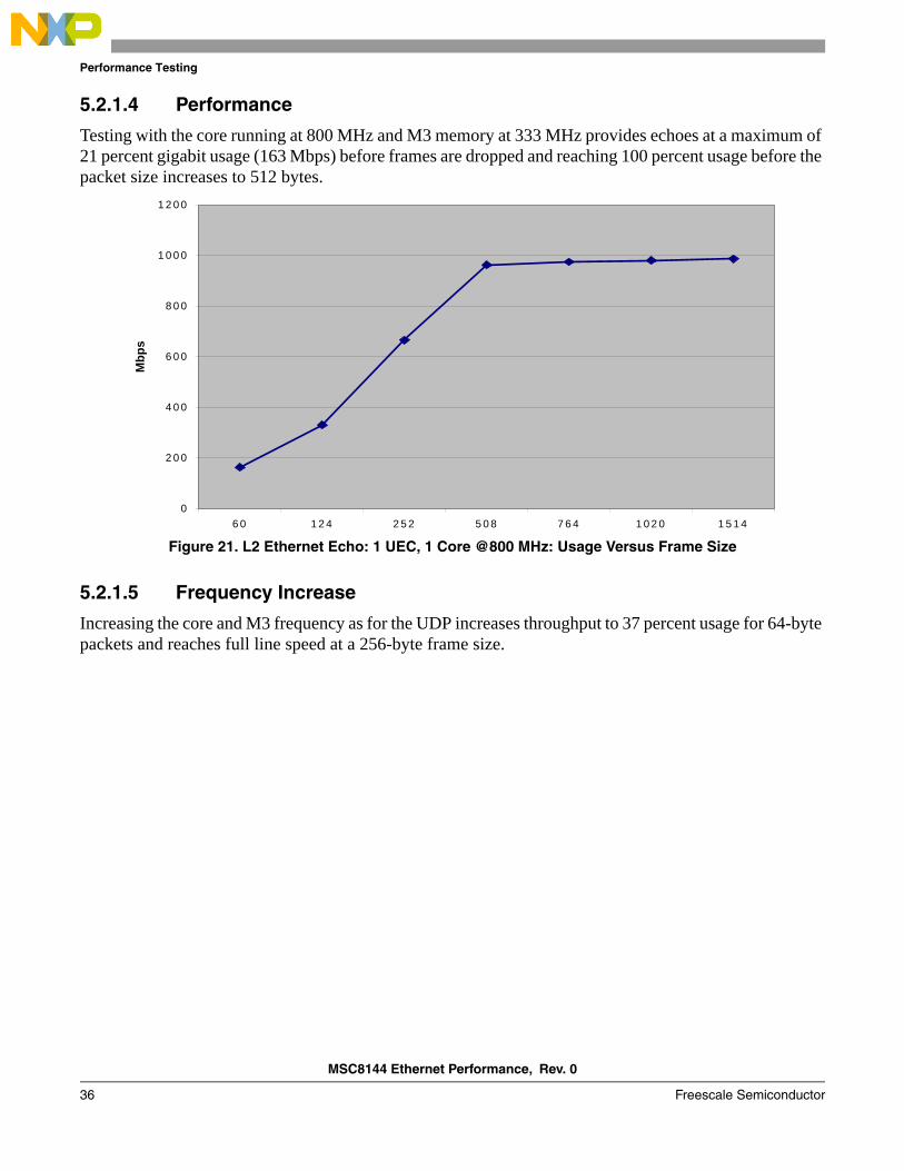
Testing with the core running at 800 MHz and M3 memory at 333 MHz provides echoes at a maximum of 21 percent gigabit usage (163 Mbps) before frames are dropped and reaching 100 percent usage before the packet size increases to 512 bytes.
Figure 21. L2 Ethernet Echo: 1 UEC, 1 Core @800 MHz: Usage Versus Frame Size
5.2.1.5 Frequency Increase
Increasing the core and M3 frequency as for the UDP increases throughput to 37 percent usage for 64-byte packets and reaches full line speed at a 256-byte frame size.
0
2 0 0
4 0 0
6 0 0
8 0 0
1 0 0 0
1 2 0 0
6 0 1 2 4 2 5 2 5 0 8 7 6 4 1 0 2 0 1 5 1 4
Mbp
s

MSC8144 Ethernet Performance, Rev. 0
Freescale Semiconductor 37
Performance Testing
Figure 22. L2 Ethernet Echo: 1 UEC, 1 Core @ 1GHz: Usage Versus Frame Size
5.2.2 Test 9: UEC L2 Echo with Four CoresFollowing the same test logic as used in the L4 UDP echo applications for purposes of comparison, the next step is to test a four-core L2 MAC-layer echo application. The register settings for the hardware in this application also mirror those of the L4 UDP echo counterpart.
5.2.2.1 SmartDSP OS Example
To use to four cores, make the following changes: • OS_NUM_OF_CORES to 4 in oc_config.c.• Re-include other executables in the target → debugger → other executables panel.
Compile and debug the project, verifying that each core’s project is set to the External Loopback target.
5.2.2.2 Performance
The four-core, single-UEC system yields slightly better results than the UDP echo with slightly less than 2 percent usage improvement to 47 percent for 64-byte frames. As with the UDP demo, full gigabit Ethernet usage is reached before frame size increases to 256 bytes.
0
200
400
600
800
1000
1200
60 124 252 508 764 1020 1514
Mbp
s
800M Hz1000M Hz

MSC8144 Ethernet Performance, Rev. 0
38 Freescale Semiconductor
Performance Testing
Figure 23. L2 Ethernet Echo: 1 UEC, 4 Core @ 1GHz: Usage Versus Frame Size
5.2.3 Test 10: UEC L2 Ethernet Loopback with Two UECsThe process of converting the L2 echo four-core project to function with two UECs is very similar to that for the UDP echo application. The differences lie in the SmartDSP OS application. The demo folder containing the required alterations to SmartDSP OS is provided in the zip file that accompanies this application note. The register programming model remains the same, as does the general idea to create a four-core system with two L2 loopback channels per core for a total of eight channels in the system.
5.2.3.1 SmartDSP OS Example
The concept of channels and cores stays the same as before (refer to Figure 14 and Section 5.1.5, “Test 5: UDP Echo using Four Cores and Both QUICC Engine UECs”). Because the L2 echo project is not identical to the UDP echo project, proceed as follows:
1. In os_config.c, enable both UECs.2. In app_config.h, create a num_channes_per_uec and a num_of_devices constant.3. In uec_demo.c, the core_channel_offset is now done in appInit, so remember to change channels
to channels/UEC.The callback function uses channel numbers, no there is no need for modifications because we handled channel numbers using the concept depicted in Figure 14.
0
200
400
600
800
1000
1200
60 124 252 508 764 1020 1514
Mbp
s 800MHz1000MHz4x 1G Cores
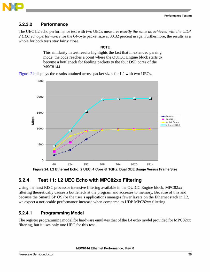
MSC8144 Ethernet Performance, Rev. 0
Freescale Semiconductor 39
Performance Testing
5.2.3.2 Performance
The UEC L2 echo performance test with two UECs measures exactly the same as achieved with the UDP 2 UEC echo performance for the 64-byte packet size at 30.32 percent usage. Furthermore, the results as a whole for both tests stay fairly close.
NOTE
This similarity in test results highlights the fact that in extended parsing mode, the code reaches a point where the QUICC Engine block starts to become a bottleneck for feeding packets to the four DSP cores of the MSC8144.
Figure 24 displays the results attained across packet sizes for L2 with two UECs.
Figure 24. L2 Ethernet Echo: 2 UEC, 4 Core @ 1GHz: Dual GbE Usage Versus Frame Size
5.2.4 Test 11: L2 UEC Echo with MPC82xx FilteringUsing the least RISC processor intensive filtering available in the QUICC Engine block, MPC82xx filtering theoretically causes a bottleneck at the program and accesses to memory. Because of this and because the SmartDSP OS (or the user’s application) manages fewer layers on the Ethernet stack in L2, we expect a noticeable performance increase when compared to UDP MPC82xx filtering.
5.2.4.1 Programming Model
The register programming model for hardware emulates that of the L4 echo model provided for MPC82xx filtering, but it uses only one UEC for this test.
0
500
1000
1500
2000
2500
60 124 252 508 764 1020 1514
Mbp
s 800MHz1000MHz4x 1G Cores4 Core 2 UEC
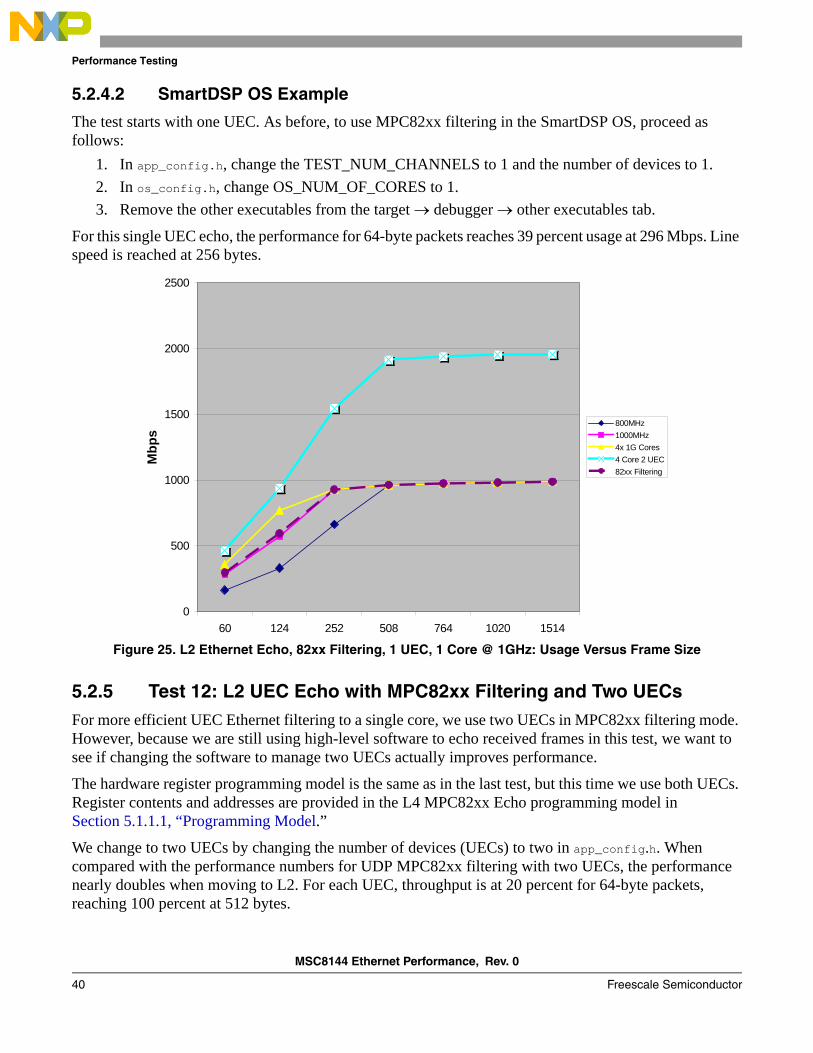
MSC8144 Ethernet Performance, Rev. 0
40 Freescale Semiconductor
Performance Testing
5.2.4.2 SmartDSP OS Example
The test starts with one UEC. As before, to use MPC82xx filtering in the SmartDSP OS, proceed as follows:
1. In app_config.h, change the TEST_NUM_CHANNELS to 1 and the number of devices to 1.2. In os_config.h, change OS_NUM_OF_CORES to 1.3. Remove the other executables from the target → debugger → other executables tab.
For this single UEC echo, the performance for 64-byte packets reaches 39 percent usage at 296 Mbps. Line speed is reached at 256 bytes.
Figure 25. L2 Ethernet Echo, 82xx Filtering, 1 UEC, 1 Core @ 1GHz: Usage Versus Frame Size
5.2.5 Test 12: L2 UEC Echo with MPC82xx Filtering and Two UECsFor more efficient UEC Ethernet filtering to a single core, we use two UECs in MPC82xx filtering mode. However, because we are still using high-level software to echo received frames in this test, we want to see if changing the software to manage two UECs actually improves performance.
The hardware register programming model is the same as in the last test, but this time we use both UECs. Register contents and addresses are provided in the L4 MPC82xx Echo programming model in Section 5.1.1.1, “Programming Model.”
We change to two UECs by changing the number of devices (UECs) to two in app_config.h. When compared with the performance numbers for UDP MPC82xx filtering with two UECs, the performance nearly doubles when moving to L2. For each UEC, throughput is at 20 percent for 64-byte packets, reaching 100 percent at 512 bytes.
0
500
1000
1500
2000
2500
60 124 252 508 764 1020 1514
Mbp
s
800MHz1000MHz4x 1G Cores4 Core 2 UEC82xx Filtering

MSC8144 Ethernet Performance, Rev. 0
Freescale Semiconductor 41
Maximizing the QUICC Engine Throughput
Figure 26. L2 Ethernet Echo, 82xx Filtering, 2 UECs, 1 Core @ 1 GHz: Dual GbE Usage Versus Frame Size
6 Maximizing the QUICC Engine ThroughputTo know how far optimization can be pushed to get maximum Ethernet throughput, we must find the theoretical limits of the MSC8144 QUICC Engine block. In extended parsing mode, this test should prove the QUICC Engine block to be the bottleneck and show that the SmartDSP OS with two UECs is truly the maximum limit of extended parsing mode. To test the theoretical limits of the QUICC Engine block, we can take the DSP core out of the bottleneck equation by not giving the DSP any Ethernet frame data movement or frame reading/writing tasks. The DSP simply passes pointers to the QUICC Engine block and frees frames from it. Although this test is based on the SmartDSP OS, this is not the way the SmartDSP OS is designed to operate, and therefore such an alteration is not supported or advised. We make the change merely to prove the limits of the QUICC Engine block for your information in this application note.
6.1 MPC82xx FilteringOur goal is to find the maximum throughput of QUICC Engine filtering for one queue. The hardware programming register model for this test is the same as that for the previous two tests using MPC82xx filtering for an L2 application. To remove the DSP load from the SmartDSP OS L2 echo code, we must make several changes to the UEC demo, including skipping some layers of the OS. This is not the recommended way to use the SmartDSP OS, but it does enable us to test the theoretical limits of the QUICC Engine block. In the uec_demo.c file, which is already set up for MPC82xx filtering for two UECs, we make the following changes:
1. Enable polling by uncommenting: #define RX_POLLING
0
500
1000
1500
2000
2500
60 124 252 508 764 1020 1514
Mbp
s
800MHz1000MHz4x 1G Cores4 Core 2 UEC82xx Filtering82xx 2 UEC

MSC8144 Ethernet Performance, Rev. 0
42 Freescale Semiconductor
Maximizing the QUICC Engine Throughput
2. Create a global variable for use as the standard send-to-QUICC Engine frame:frame_data[0x100] = { insert the contents for a standard frame you will repeatedly send to the QUICC Engine block here }
#pragma align frame_data ARCH_CACHE_LINE_SIZE
3. Use the prepare_bds function to initialize the TxBDs to point to the buffer (frame) just created: void prepare_bds(void *ch_handle)
{
msc814x_uec_tx_channel_t *tx_ch = (msc814x_uec_tx_channel_t *)ch_handle;uint8_t *bd; void* frame_data_phys;uint32_t bd_status;
bd = tx_ch->tx_base;osMmuDataVirtToPhys(frame_data, &frame_data_phys);while(1)
{
UEC_BD_BUFFER_SET(bd, (uint8_t *)frame_data_phys);bd_status = UEC_BD_STATUS_AND_LENGTH(bd);if(bd_status & T_W) break;bd += UEC_BD_SIZE;
}}
This program uses a transmit function to bypass the SmartDSP OS BIO layer and simply pass a pointer to the TxBDs. The my_uecChannelTx function is based on the uecChannelTx() in the SmartDSP OS MSC8144 driver library. The receive callback function has been updated to skip the BIO layer and directly call the my_uecChannelTx function similarly to the transmit function. This function POLLs the receive channel for new frames.
4. For appInit(), make the following changes:a) Change the callback functions to = NULL (using polling).b) After the Tx channels are set, use prepare_bds.c) Turn off cache coherency because the concern is not whether the DSP receives the correct
data, but simply to maximize the throughput of the QUICC Engine block.appBackground() constantly calls the receive polling function and then the transmit function. Therefore, the received frame is not echoed but sends the default global frame for every received frame <TBD>.
These changes enable us to find the theoretical limit of the QUICC Engine block in MPC82xx filtering mode. For one UEC, the QUICC Engine block reaches 100 percent utility, as indicated by the SmartBits tester, at 64-byte frames. The effective bit rate is near 800 Mbps instead of 1Gbps because the interframe gap is cumulatively larger for the smaller frame size.

MSC8144 Ethernet Performance, Rev. 0
Freescale Semiconductor 43
Maximizing the QUICC Engine Throughput
Figure 27. L2 Ethernet I/O: QUICC Engine Max 82xx: 1 UEC, 1 Core @ 1GHz: Usage Versus Frame Size
For two UECs, the QUICC Engine block reaches its limits for 64-byte frames before it reaches 100 percent utility (at 66 percent and a 490 Mbps frame rate per UEC). In this system, the QUICC Engine reaches 100 percent usage at a frame length of 124 bytes. This is the true limit of the QUICC Engine system on the MSC8144 when filtering to a single core.
Figure 28. L2 Ethernet I/O: QUICC Engine Max 82xx: 2 UEC, 1 Core @ 1GHz: Usage Versus Frame
0
200
400
600
800
1000
1200
60 124 252 508 764 1020 1514
Mbp
s
82xx 1 UEC Limits
0
500
1000
1500
2000
2500
60 124 252 508 764 1020 1514
Mbp
s
82xx 1 UEC82xx 2 UEC
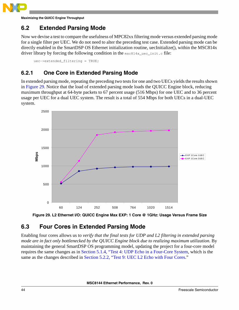
MSC8144 Ethernet Performance, Rev. 0
44 Freescale Semiconductor
Maximizing the QUICC Engine Throughput
6.2 Extended Parsing ModeNow we devise a test to compare the usefulness of MPC82xx filtering mode versus extended parsing mode for a single filter per UEC. We do not need to alter the preceding test case. Extended parsing mode can be directly enabled in the SmartDSP OS Ethernet initialization routine, uecInitialize(), within the MSC814x driver library by forcing the following condition in the msc814x_uec_init.c file:
uec->extended_filtering = TRUE;
6.2.1 One Core in Extended Parsing ModeIn extended parsing mode, repeating the preceding two tests for one and two UECs yields the results shown in Figure 29. Notice that the load of extended parsing mode loads the QUICC Engine block, reducing maximum throughput at 64-byte packets to 67 percent usage (516 Mbps) for one UEC and to 36 percent usage per UEC for a dual UEC system. The result is a total of 554 Mbps for both UECs in a dual-UEC system.
Figure 29. L2 Ethernet I/O: QUICC Engine Max EXP: 1 Core @ 1GHz: Usage Versus Frame Size
6.3 Four Cores in Extended Parsing ModeEnabling four cores allows us to verify that the final tests for UDP and L2 filtering in extended parsing mode are in fact only bottlenecked by the QUICC Engine block due to realizing maximum utilization. By maintaining the general SmartDSP OS programming model, updating the project for a four-core model requires the same changes as in Section 5.1.4, “Test 4: UDP Echo in a Four-Core System, which is the same as the changes described in Section 5.2.2, “Test 9: UEC L2 Echo with Four Cores.”
0
500
1000
1500
2000
2500
60 124 252 508 764 1020 1514
Mbp
s
EXP 1Core 1UECEXP 1Core 2UEC
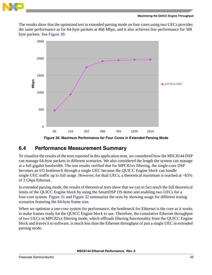
MSC8144 Ethernet Performance, Rev. 0
Freescale Semiconductor 45
Maximizing the QUICC Engine Throughput
The results show that the optimized test in extended parsing mode on four cores using two UECs provides the same performance as for 64-byte packets at 468 Mbps, and it also achieves line performance for 508 byte packets. See Figure 30.
Figure 30. Maximum Performance for Four Cores in Extended Parsing Mode
6.4 Performance Measurement SummaryTo visualize the results of the tests reported in this application note, we considered how the MSC8144 DSP can manage 64-byte packets in different scenarios. We also considered the length the system can manage at a full gigabit bandwidth. The test results verified that for MPC82xx filtering, the single-core DSP becomes an I/O bottleneck through a single UEC because the QUICC Engine block can handle single-UEC traffic up to full usage. However, for dual UECs, a theoretical maximum is reached at ~65% of 2 Gbps Ethernet.
In extended parsing mode, the results of theoretical tests show that we can in fact reach the full theoretical limits of the QUICC Engine block by using the SmartDSP OS demo and enabling two UECs for a four-core system. Figure 31 and Figure 32 summarize the tests by showing usage for different testing scenarios featuring the 64-byte frame size.
When we optimize a one-core system for performance, the bottleneck for Ethernet is the core as it works to make frames ready for the QUICC Engine block to use. Therefore, the cumulative Ethernet throughput of two UECs in MPC82xx filtering mode, which offloads filtering functionality from the QUICC Engine block and leaves it to software, is much less than the Ethernet throughput of just a single UEC in extended parsing mode.
0
500
1000
1500
2000
2500
60 124 252 508 764 1020 1514
Mbp
s
EXP 4Core 2UEC
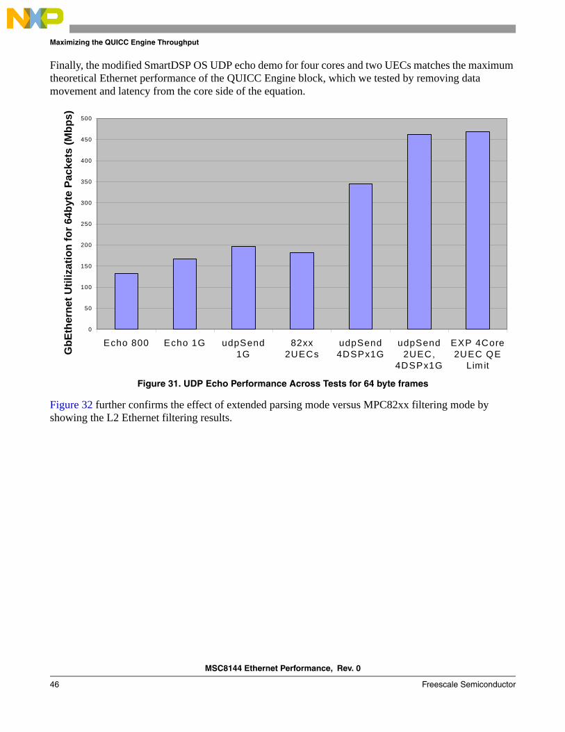
MSC8144 Ethernet Performance, Rev. 0
46 Freescale Semiconductor
Maximizing the QUICC Engine Throughput
Finally, the modified SmartDSP OS UDP echo demo for four cores and two UECs matches the maximum theoretical Ethernet performance of the QUICC Engine block, which we tested by removing data movement and latency from the core side of the equation.
Figure 31. UDP Echo Performance Across Tests for 64 byte frames
Figure 32 further confirms the effect of extended parsing mode versus MPC82xx filtering mode by showing the L2 Ethernet filtering results.
0
50
100
150
200
250
300
350
400
450
500
Echo 800 Echo 1G udpSend1G
82xx2UECs
udpSend4DSPx1G
udpSend2UEC,
4DSPx1G
EXP 4Core2UEC QE
Lim it
GbE
ther
net U
tiliz
atio
n fo
r 64b
yte
Pack
ets
(Mbp
s)
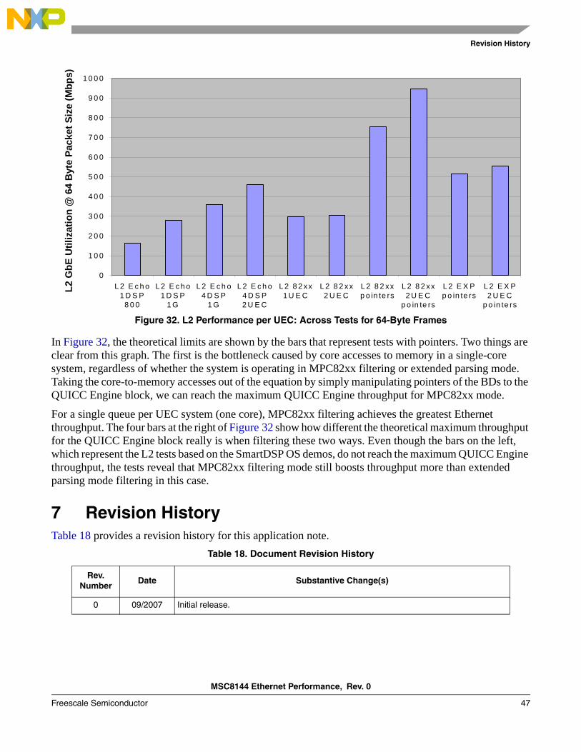
MSC8144 Ethernet Performance, Rev. 0
Freescale Semiconductor 47
Revision History
Figure 32. L2 Performance per UEC: Across Tests for 64-Byte Frames
In Figure 32, the theoretical limits are shown by the bars that represent tests with pointers. Two things are clear from this graph. The first is the bottleneck caused by core accesses to memory in a single-core system, regardless of whether the system is operating in MPC82xx filtering or extended parsing mode. Taking the core-to-memory accesses out of the equation by simply manipulating pointers of the BDs to the QUICC Engine block, we can reach the maximum QUICC Engine throughput for MPC82xx mode.
For a single queue per UEC system (one core), MPC82xx filtering achieves the greatest Ethernet throughput. The four bars at the right of Figure 32 show how different the theoretical maximum throughput for the QUICC Engine block really is when filtering these two ways. Even though the bars on the left, which represent the L2 tests based on the SmartDSP OS demos, do not reach the maximum QUICC Engine throughput, the tests reveal that MPC82xx filtering mode still boosts throughput more than extended parsing mode filtering in this case.
7 Revision History Table 18 provides a revision history for this application note.
Table 18. Document Revision History
Rev.Number
Date Substantive Change(s)
0 09/2007 Initial release.
0
1 0 0
2 0 0
3 0 0
4 0 0
5 0 0
6 0 0
7 0 0
8 0 0
9 0 0
1 0 0 0
L 2 E c h o1 D S P
8 0 0
L 2 E c h o1 D S P
1 G
L 2 E c h o4 D S P
1 G
L 2 E c h o4 D S P2 U E C
L 2 8 2 xx1 U E C
L 2 8 2 xx2 U E C
L 2 8 2 xxp o in te rs
L 2 8 2 xx2 U E C
p o in te rs
L 2 E X Pp o in te rs
L 2 E X P2 U E C
p o in te rs
L2 G
bE U
tiliz
atio
n @
64
Byt
e Pa
cket
Siz
e (M
bps)
Document Number: AN3439Rev. 009/2007
Information in this document is provided solely to enable system and software
implementers to use Freescale Semiconductor products. There are no express or
implied copyright licenses granted hereunder to design or fabricate any integrated
circuits or integrated circuits based on the information in this document.
Freescale Semiconductor reserves the right to make changes without further notice to
any products herein. Freescale Semiconductor makes no warranty, representation or
guarantee regarding the suitability of its products for any particular purpose, nor does
Freescale Semiconductor assume any liability arising out of the application or use of
any product or circuit, and specifically disclaims any and all liability, including without
limitation consequential or incidental damages. “Typical” parameters which may be
provided in Freescale Semiconductor data sheets and/or specifications can and do
vary in different applications and actual performance may vary over time. All operating
parameters, including “Typicals” must be validated for each customer application by
customer’s technical experts. Freescale Semiconductor does not convey any license
under its patent rights nor the rights of others. Freescale Semiconductor products are
not designed, intended, or authorized for use as components in systems intended for
surgical implant into the body, or other applications intended to support or sustain life,
or for any other application in which the failure of the Freescale Semiconductor product
could create a situation where personal injury or death may occur. Should Buyer
purchase or use Freescale Semiconductor products for any such unintended or
unauthorized application, Buyer shall indemnify and hold Freescale Semiconductor
and its officers, employees, subsidiaries, affiliates, and distributors harmless against all
claims, costs, damages, and expenses, and reasonable attorney fees arising out of,
directly or indirectly, any claim of personal injury or death associated with such
unintended or unauthorized use, even if such claim alleges that Freescale
Semiconductor was negligent regarding the design or manufacture of the part.
How to Reach Us:
Home Page: www.freescale.com
Web Support: http://www.freescale.com/support
USA/Europe or Locations Not Listed: Freescale Semiconductor, Inc.Technical Information Center, EL5162100 East Elliot Road Tempe, Arizona 85284 +1-800-521-6274 or+1-480-768-2130www.freescale.com/support
Europe, Middle East, and Africa:Freescale Halbleiter Deutschland GmbHTechnical Information CenterSchatzbogen 781829 Muenchen, Germany+44 1296 380 456 (English) +46 8 52200080 (English)+49 89 92103 559 (German)+33 1 69 35 48 48 (French) www.freescale.com/support
Japan: Freescale Semiconductor Japan Ltd. HeadquartersARCO Tower 15F1-8-1, Shimo-Meguro, Meguro-ku Tokyo 153-0064Japan 0120 191014 or+81 3 5437 [email protected]
Asia/Pacific: Freescale Semiconductor Hong Kong Ltd. Technical Information Center2 Dai King Street Tai Po Industrial Estate Tai Po, N.T., Hong Kong +800 2666 [email protected]
For Literature Requests Only:Freescale Semiconductor
Literature Distribution Center P.O. Box 5405Denver, Colorado 80217 +1-800 441-2447 or+1-303-675-2140Fax: +1-303-675-2150LDCForFreescaleSemiconductor
@hibbertgroup.com
Freescale™, the Freescale logo, and PowerQUICC are trademarks and StarCore is a registered trademark of Freescale Semiconductor, Inc. CodeWarrior is a trademark or registered trademark of Freescale Semiconductor, Inc. in the United States and/or other countries. All other product or service names are the property of their respective owners.
© Freescale Semiconductor, Inc., 2007. All rights reserved.
THIS PAGE INTENTIONALLY LEFT BLANK
Related Documents