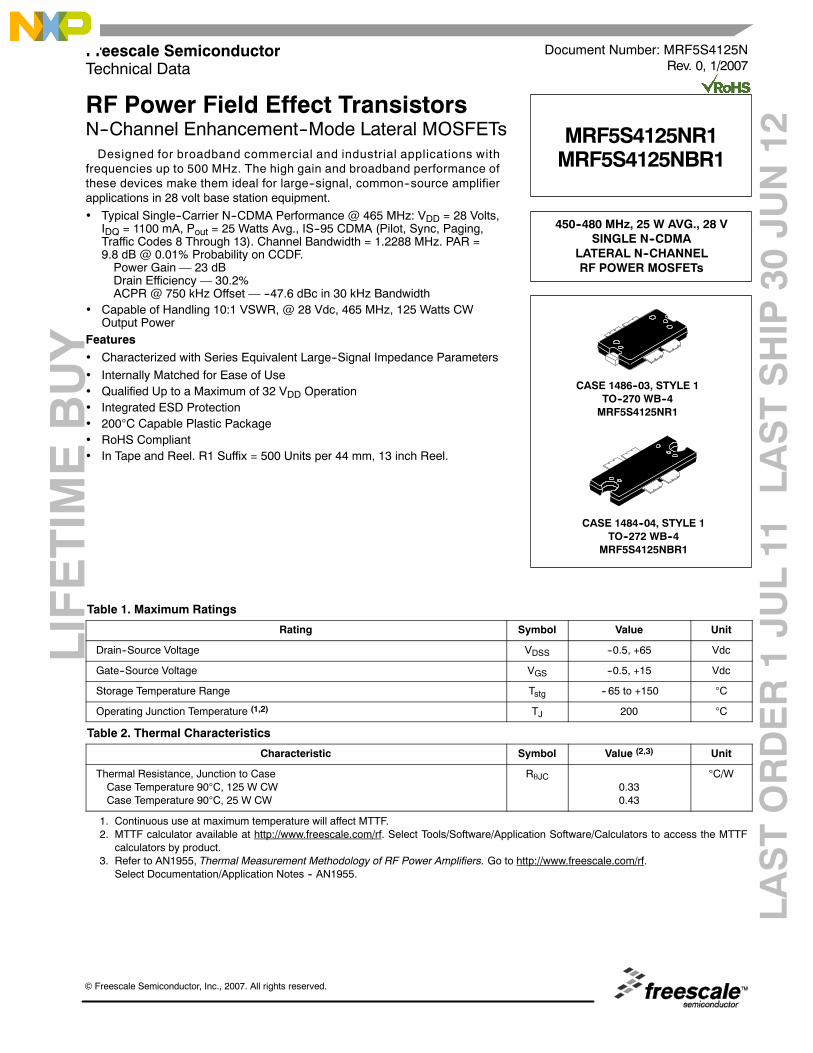
RF Power Field Effect Transistors N--Channel Enhancement--Mode Lateral MOSFETs Designed for broadband commercial and industrial applications with frequencies up to 500 MHz. The high gain and broadband performance of these devices make them ideal for large--signal, common--source amplifier applications in 28 volt base station equipment. • Typical Single--Carrier N--CDMA Performance @ 465 MHz: V DD = 28 Volts, I DQ = 1100 mA, P out = 25 Watts Avg., IS--95 CDMA (Pilot, Sync, Paging, Traffic Codes 8 Through 13). Channel Bandwidth = 1.2288 MHz. PAR = 9.8 dB @ 0.01% Probability on CCDF. Power Gain 23 dB Drain Efficiency 30.2% ACPR @ 750 kHz Offset --47.6 dBc in 30 kHz Bandwidth • Capable of Handling 10:1 VSWR, @ 28 Vdc, 465 MHz, 125 Watts CW Output Power Features • Characterized with Series Equivalent Large--Signal Impedance Parameters • Internally Matched for Ease of Use • Qualified Up to a Maximum of 32 V DD Operation • Integrated ESD Protection • 200°C Capable Plastic Package • RoHS Compliant • In Tape and Reel. R1 Suffix = 500 Units per 44 mm, 13 inch Reel. Table 1. Maximum Ratings Rating Symbol Value Unit Drain--Source Voltage V DSS --0.5, +65 Vdc Gate--Source Voltage V GS --0.5, +15 Vdc Storage Temperature Range T stg --65 to +150 °C Operating Junction Temperature (1,2) T J 200 °C Table 2. Thermal Characteristics Characteristic Symbol Value (2,3) Unit Thermal Resistance, Junction to Case Case Temperature 90°C, 125 W CW Case Temperature 90°C, 25 W CW R θJC 0.33 0.43 °C/W 1. Continuous use at maximum temperature will affect MTTF. 2. MTTF calculator available at http://www.freescale.com/rf . Select Tools/Software/Application Software/Calculators to access the MTTF calculators by product. 3. Refer to AN1955, Thermal Measurement Methodology of RF Power Amplifiers. Go to http://www.freescale.com/rf . Select Documentation/Application Notes -- AN1955. LIFETIME BUY LAST ORDER 1 JUL 11 LAST SHIP 30 JUN 12 Document Number: MRF5S4125N Rev. 0, 1/2007 Freescale Semiconductor Technical Data MRF5S4125NR1 MRF5S4125NBR1 450--480 MHz, 25 W AVG., 28 V SINGLE N--CDMA LATERAL N--CHANNEL RF POWER MOSFETs CASE 1484--04, STYLE 1 TO--272 WB--4 MRF5S4125NBR1 CASE 1486--03, STYLE 1 TO--270 WB--4 MRF5S4125NR1 © Freescale Semiconductor, Inc., 2007. All rights reserved.

Welcome message from author
This document is posted to help you gain knowledge. Please leave a comment to let me know what you think about it! Share it to your friends and learn new things together.
Transcript
MRF5S4125NR1 MRF5S4125NBR1
1RF Device DataFreescale Semiconductor
RF Power Field Effect TransistorsN--Channel Enhancement--Mode Lateral MOSFETsDesigned for broadband commercial and industrial applications with
frequencies up to 500 MHz. The high gain and broadband performance ofthese devices make them ideal for large--signal, common--source amplifierapplications in 28 volt base station equipment.
• Typical Single--Carrier N--CDMA Performance @ 465 MHz: VDD = 28 Volts,IDQ = 1100 mA, Pout = 25 Watts Avg., IS--95 CDMA (Pilot, Sync, Paging,Traffic Codes 8 Through 13). Channel Bandwidth = 1.2288 MHz. PAR =9.8 dB @ 0.01% Probability on CCDF.Power Gain 23 dBDrain Efficiency 30.2%ACPR @ 750 kHz Offset --47.6 dBc in 30 kHz Bandwidth
• Capable of Handling 10:1 VSWR, @ 28 Vdc, 465 MHz, 125 Watts CWOutput Power
Features• Characterized with Series Equivalent Large--Signal Impedance Parameters
• Internally Matched for Ease of Use• Qualified Up to a Maximum of 32 VDD Operation• Integrated ESD Protection• 200°C Capable Plastic Package• RoHS Compliant• In Tape and Reel. R1 Suffix = 500 Units per 44 mm, 13 inch Reel.
Table 1. Maximum Ratings
Rating Symbol Value Unit
Drain--Source Voltage VDSS --0.5, +65 Vdc
Gate--Source Voltage VGS --0.5, +15 Vdc
Storage Temperature Range Tstg -- 65 to +150 °C
Operating Junction Temperature (1,2) TJ 200 °C
Table 2. Thermal Characteristics
Characteristic Symbol Value (2,3) Unit
Thermal Resistance, Junction to CaseCase Temperature 90°C, 125 W CWCase Temperature 90°C, 25 W CW
RθJC0.330.43
°C/W
1. Continuous use at maximum temperature will affect MTTF.2. MTTF calculator available at http://www.freescale.com/rf. Select Tools/Software/Application Software/Calculators to access the MTTF
calculators by product.3. Refer to AN1955, Thermal Measurement Methodology of RF Power Amplifiers. Go to http://www.freescale.com/rf.
Select Documentation/Application Notes -- AN1955.
LIFETIMEBUY
LASTORDER1JU
L11
LASTSHIP
30JU
N12
Document Number: MRF5S4125NRev. 0, 1/2007
Freescale SemiconductorTechnical Data
MRF5S4125NR1MRF5S4125NBR1
450--480 MHz, 25 W AVG., 28 VSINGLE N--CDMA
LATERAL N--CHANNELRF POWER MOSFETs
CASE 1484--04, STYLE 1TO--272 WB--4
MRF5S4125NBR1
CASE 1486--03, STYLE 1TO--270 WB--4MRF5S4125NR1
© Freescale Semiconductor, Inc., 2007. All rights reserved.
2RF Device Data
Freescale Semiconductor
MRF5S4125NR1 MRF5S4125NBR1
Table 3. ESD Protection Characteristics
Test Methodology Class
Human Body Model (per JESD22--A114) 1B (Minimum)
Machine Model (per EIA/JESD22--A115) A (Minimum)
Charge Device Model (per JESD22--C101) IV (Minimum)
Table 4. Moisture Sensitivity Level
Test Methodology Rating Package Peak Temperature Unit
Per JESD 22--A113, IPC/JEDEC J--STD--020 3 260 °C
Table 5. Electrical Characteristics (TC = 25°C unless otherwise noted)
Characteristic Symbol Min Typ Max Unit
Off Characteristics
Zero Gate Voltage Drain Leakage Current(VDS = 65 Vdc, VGS = 0 Vdc)
IDSS 10 μAdc
Zero Gate Voltage Drain Leakage Current(VDS = 28 Vdc, VGS = 0 Vdc)
IDSS 1 μAdc
Gate--Source Leakage Current(VGS = 5 Vdc, VDS = 0 Vdc)
IGSS 10 μAdc
On Characteristics
Gate Threshold Voltage(VDS = 10 Vdc, ID = 400 μAdc)
VGS(th) 2 3 4 Vdc
Gate Quiescent Voltage(VDS = 28 Vdc, ID = 1100 mAdc, Measured in Functional Test)
VGS(Q) 3.5 4.25 5 Vdc
Drain--Source On--Voltage(VGS = 10 Vdc, ID = 1.5 Adc)
VDS(on) 0.05 0.175 0.3 Vdc
Dynamic Characteristics (1)
Reverse Transfer Capacitance(VDS = 28 Vdc ± 30 mV(rms)ac @ 1 MHz, VGS = 0 Vdc)
Crss 2.41 pF
Output Capacitance(VDS = 28 Vdc ± 30 mV(rms)ac @ 1 MHz, VGS = 0 Vdc)
Coss 74.61 pF
Functional Tests (In Freescale Test Fixture, 50 ohm system) VDD = 28 Vdc, IDQ = 1100 mA, Pout = 25 W Avg. N--CDMA, f = 465 MHz,Single--Carrier N--CDMA, 1.2288 MHz Channel Bandwidth Carrier. ACPR measured in 30 kHz Channel Bandwidth @ ±750 kHz Offset.PAR = 9.8 dB @ 0.01% Probability on CCDF.
Power Gain Gps 22 23 25 dB
Drain Efficiency ηD 28 30.2 %
Adjacent Channel Power Ratio ACPR --47.6 --45 dBc
Input Return Loss IRL --15 --9 dB
1. Part internally input matched.
LIFETIMEBUY
LASTORDER1JU
L11
LASTSHIP
30JU
N12
MRF5S4125NR1 MRF5S4125NBR1
3RF Device DataFreescale Semiconductor
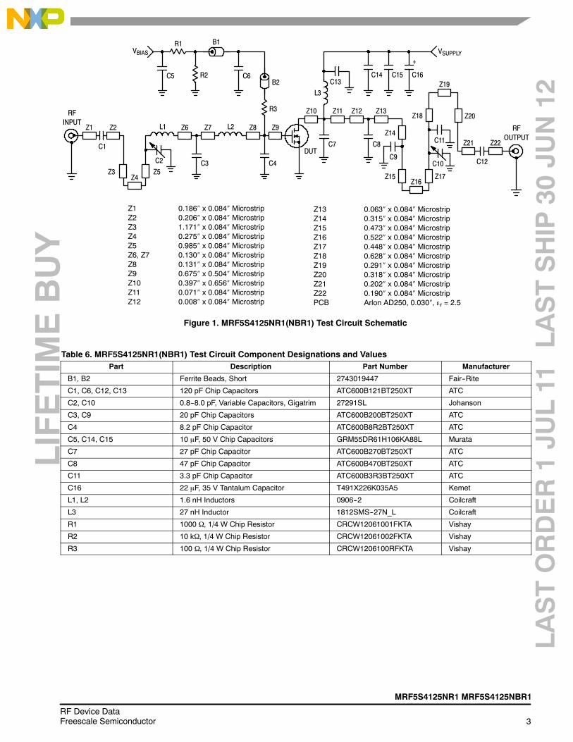
Figure 1. MRF5S4125NR1(NBR1) Test Circuit Schematic
RFINPUT
RFOUTPUT
C1
VSUPPLYVBIAS
Z7 Z9
DUT
Z6
Z4
Z8L1Z1 Z2
Z3
C5
B1R1
R2 C6B2
R3
Z5C3C2
L2
C4
Z10
C8C7
L3
C13
Z11 Z12 Z13
Z16
Z14
Z17
C9
Z15
C14 C15 C16
+
C10
C11
Z18
Z19
Z20
Z21 Z22
C12
Z1 0.186″ x 0.084″ MicrostripZ2 0.206″ x 0.084″ MicrostripZ3 1.171″ x 0.084″ MicrostripZ4 0.275″ x 0.084″ MicrostripZ5 0.985″ x 0.084″ MicrostripZ6, Z7 0.130″ x 0.084″ MicrostripZ8 0.131″ x 0.084″ MicrostripZ9 0.675″ x 0.504″ MicrostripZ10 0.397″ x 0.656″ MicrostripZ11 0.071″ x 0.084″ MicrostripZ12 0.008″ x 0.084″ Microstrip
Z13 0.063″ x 0.084″ MicrostripZ14 0.315″ x 0.084″ MicrostripZ15 0.473″ x 0.084″ MicrostripZ16 0.522″ x 0.084″ MicrostripZ17 0.448″ x 0.084″ MicrostripZ18 0.628″ x 0.084″ MicrostripZ19 0.291″ x 0.084″ MicrostripZ20 0.318″ x 0.084″ MicrostripZ21 0.202″ x 0.084″ MicrostripZ22 0.190″ x 0.084″ MicrostripPCB Arlon AD250, 0.030″, εr = 2.5
Table 6. MRF5S4125NR1(NBR1) Test Circuit Component Designations and ValuesPart Description Part Number Manufacturer
B1, B2 Ferrite Beads, Short 2743019447 Fair--Rite
C1, C6, C12, C13 120 pF Chip Capacitors ATC600B121BT250XT ATC
C2, C10 0.8--8.0 pF, Variable Capacitors, Gigatrim 27291SL Johanson
C3, C9 20 pF Chip Capacitors ATC600B200BT250XT ATC
C4 8.2 pF Chip Capacitor ATC600B8R2BT250XT ATC
C5, C14, C15 10 μF, 50 V Chip Capacitors GRM55DR61H106KA88L Murata
C7 27 pF Chip Capacitor ATC600B270BT250XT ATC
C8 47 pF Chip Capacitor ATC600B470BT250XT ATC
C11 3.3 pF Chip Capacitor ATC600B3R3BT250XT ATC
C16 22 μF, 35 V Tantalum Capacitor T491X226K035A5 Kemet
L1, L2 1.6 nH Inductors 0906--2 Coilcraft
L3 27 nH Inductor 1812SMS--27N_L Coilcraft
R1 1000 Ω, 1/4 W Chip Resistor CRCW12061001FKTA Vishay
R2 10 kΩ, 1/4 W Chip Resistor CRCW12061002FKTA Vishay
R3 100 Ω, 1/4 W Chip Resistor CRCW1206100RFKTA Vishay
LIFETIMEBUY
LASTORDER1JU
L11
LASTSHIP
30JU
N12
4RF Device Data
Freescale Semiconductor
MRF5S4125NR1 MRF5S4125NBR1
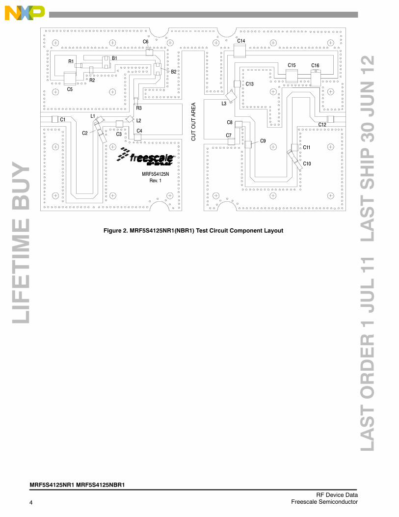
Figure 2. MRF5S4125NR1(NBR1) Test Circuit Component Layout
CUTOUTAREA
C6
MRF5S4125NRev. 1
R1
R2
C5
B1
B2
R3
L2
C3C4C2
L1C1
C10
C7C9
C11
C8
L3
C12
C16C15
C13
C14
LIFETIMEBUY
LASTORDER1JU
L11
LASTSHIP
30JU
N12
MRF5S4125NR1 MRF5S4125NBR1
5RF Device DataFreescale Semiconductor
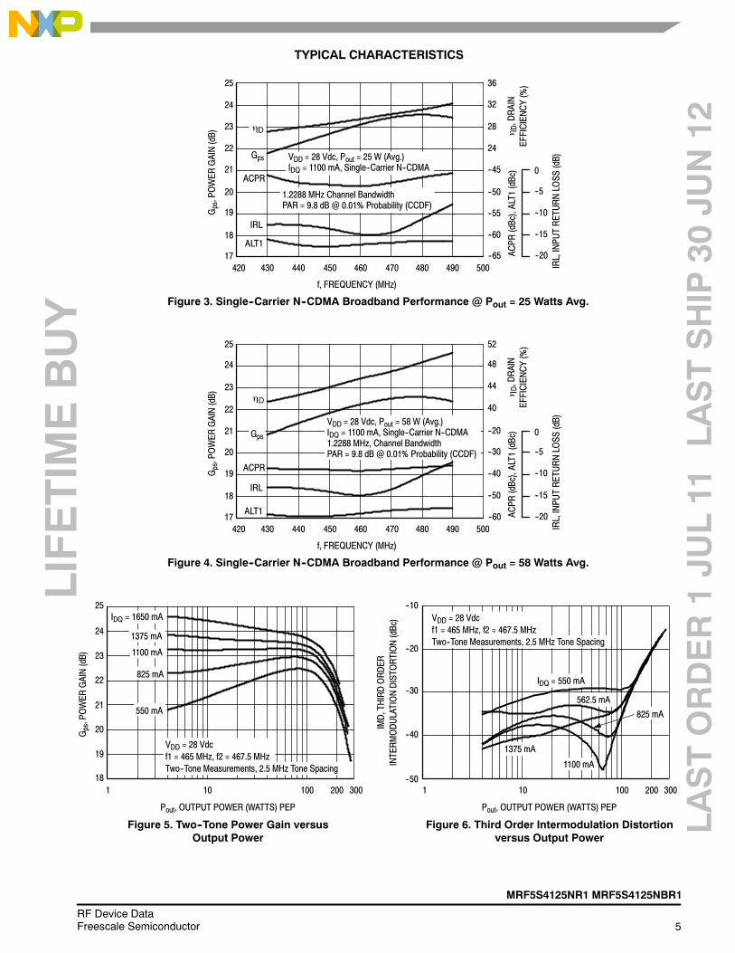
TYPICAL CHARACTERISTICS
IRL,INPUTRETURNLOSS
(dB)
ACPR
(dBc),ALT1(dBc)
500420
IRL
Gps
ACPR
ALT1
f, FREQUENCY (MHz)
Figure 3. Single--Carrier N--CDMA Broadband Performance @ Pout = 25 Watts Avg.
--20
0
--10
--5
VDD = 28 Vdc, Pout = 25 W (Avg.)IDQ = 1100 mA, Single--Carrier N--CDMA
48046044017
25
--65
36
32
28
--45
--50
--55
--60
ηD,DRAIN
EFFICIENCY(%)
ηD
Gps,POWER
GAIN(dB)
24
23
22
21
20
19
18
430 450 470 490
24
--15
IRL,INPUTRETURNLOSS
(dB)
ACPR
(dBc),ALT1(dBc)
500420
IRL
Gps
ACPR
ALT1
f, FREQUENCY (MHz)
Figure 4. Single--Carrier N--CDMA Broadband Performance @ Pout = 58 Watts Avg.
--20
0
--5
--10
48046044017
25
--60
52
48
44
--20
--30
--40
--50
ηD,DRAIN
EFFICIENCY(%)
ηD
Gps,POWER
GAIN(dB)
24
23
22
21
20
19
18
430 450 470 490
40
--15
Figure 5. Two--Tone Power Gain versusOutput Power
10018
25
1
IDQ = 1650 mA
1375 mA24
23
21
10 300
Pout, OUTPUT POWER (WATTS) PEP
Gps,POWER
GAIN(dB)
20
22825 mA
550 mA
Figure 6. Third Order Intermodulation Distortionversus Output Power
--10
1 100
--20
--30
--40
300--50
10
Pout, OUTPUT POWER (WATTS) PEP
INTERMODULATIONDISTORTION(dBc)
IMD,THIRDORDER
IDQ = 550 mA
1100 mA
825 mA
562.5 mA
1.2288 MHz Channel BandwidthPAR = 9.8 dB @ 0.01% Probability (CCDF)
19
200
VDD = 28 Vdcf1 = 465 MHz, f2 = 467.5 MHzTwo--Tone Measurements, 2.5 MHz Tone Spacing
1100 mA
200
VDD = 28 Vdcf1 = 465 MHz, f2 = 467.5 MHzTwo--Tone Measurements, 2.5 MHz Tone Spacing
1375 mA
VDD = 28 Vdc, Pout = 58 W (Avg.)IDQ = 1100 mA, Single--Carrier N--CDMA1.2288 MHz, Channel BandwidthPAR = 9.8 dB @ 0.01% Probability (CCDF)
LIFETIMEBUY
LASTORDER1JU
L11
LASTSHIP
30JU
N12
6RF Device Data
Freescale Semiconductor
MRF5S4125NR1 MRF5S4125NBR1
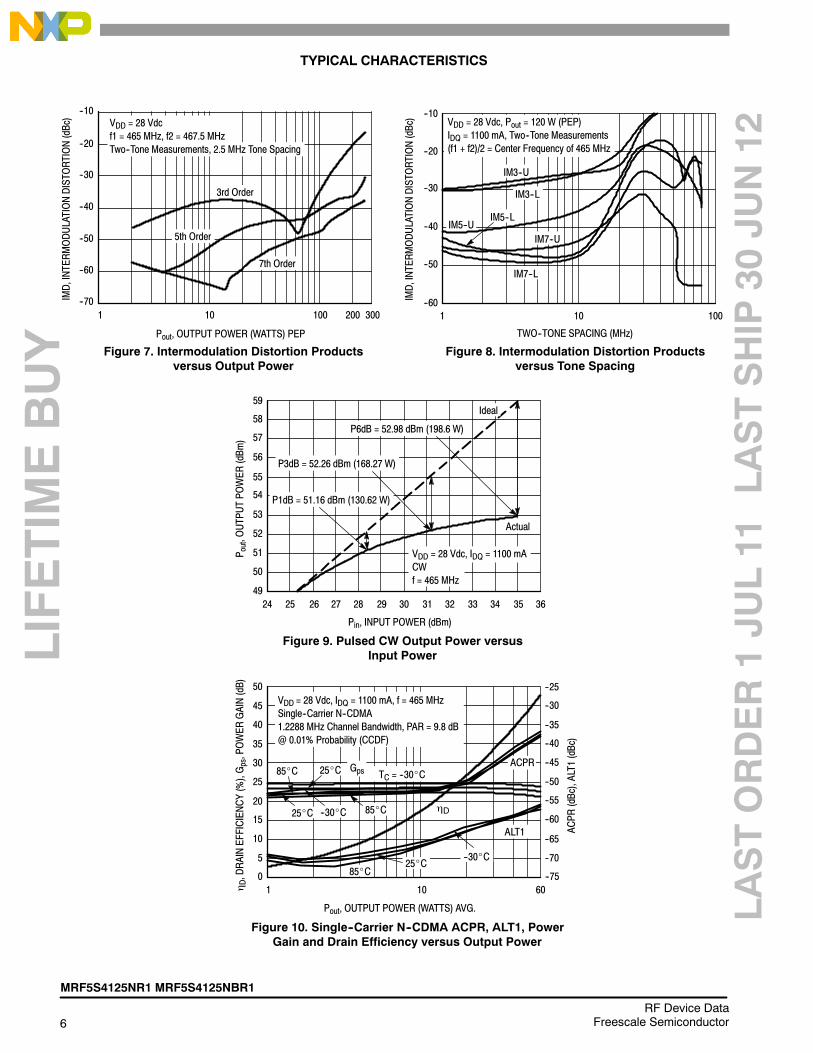
TYPICAL CHARACTERISTICS
Figure 7. Intermodulation Distortion Productsversus Output Power
Pout, OUTPUT POWER (WATTS) PEP
IMD,INTERMODULATIONDISTORTION(dBc)
--70
--10
1 100
--40
--50
10
--30
--20
7th Order
5th Order
3rd Order
Figure 8. Intermodulation Distortion Productsversus Tone Spacing
10
TWO--TONE SPACING (MHz)
IM7--L
--30
--40
--50
1 100
IMD,INTERMODULATIONDISTORTION(dBc)
Figure 9. Pulsed CW Output Power versusInput Power
36
59
25
Pin, INPUT POWER (dBm)
56
54
52
26 2827 3029 3331
Actual
Ideal
P1dB = 51.16 dBm (130.62 W)
57
53
55
32 3424
P out,OUTPUTPOWER
(dBm
)
P6dB = 52.98 dBm (198.6 W)
Figure 10. Single--Carrier N--CDMA ACPR, ALT1, PowerGain and Drain Efficiency versus Output Power
0 --75
Pout, OUTPUT POWER (WATTS) AVG.
50 --25
25
--35
20
--40
15
--55
5 --70
1 10
--60
10
ηD
Gps TC = --30_CACPR
ηD,DRAINEFFICIENCY(%),Gps,POWER
GAIN(dB)
ACPR
(dBc),ALT1(dBc)
50
P3dB = 52.26 dBm (168.27 W)
300
IM7--U
IM5--LIM5--U
IM3--L
IM3--U
--20
--10
35
51
30
35
40
45
--65
--50
--45
--30
25_C85_C
VDD = 28 Vdc, IDQ = 1100 mA, f = 465 MHzSingle--Carrier N--CDMA1.2288 MHz Channel Bandwidth, PAR = 9.8 dB@ 0.01% Probability (CCDF)
49
--30_C
--60
200
VDD = 28 Vdcf1 = 465 MHz, f2 = 467.5 MHzTwo--Tone Measurements, 2.5 MHz Tone Spacing
--60
58
ALT1
85_C25_C
--30_C85_C
25_C
VDD = 28 Vdc, Pout = 120 W (PEP)IDQ = 1100 mA, Two--Tone Measurements(f1 + f2)/2 = Center Frequency of 465 MHz
60
VDD = 28 Vdc, IDQ = 1100 mACWf = 465 MHz
LIFETIMEBUY
LASTORDER1JU
L11
LASTSHIP
30JU
N12
MRF5S4125NR1 MRF5S4125NBR1
7RF Device DataFreescale Semiconductor
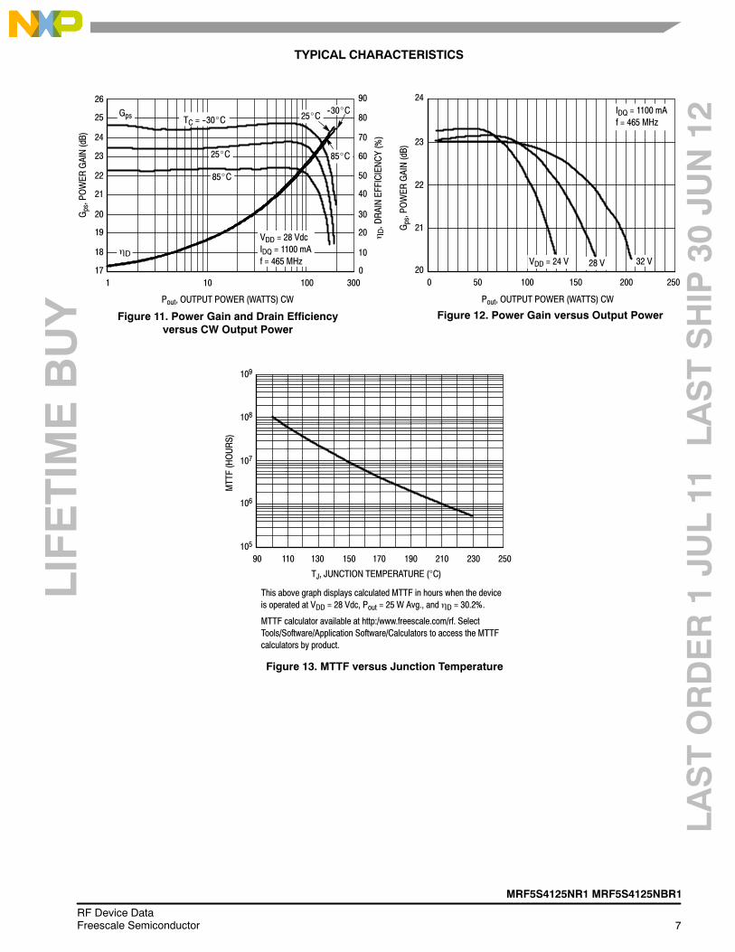
TYPICAL CHARACTERISTICS
This above graph displays calculated MTTF in hours when the deviceis operated at VDD = 28 Vdc, Pout = 25 W Avg., and ηD = 30.2%.
MTTF calculator available at http:/www.freescale.com/rf. SelectTools/Software/Application Software/Calculators to access the MTTFcalculators by product.
100171
0
90
Pout, OUTPUT POWER (WATTS) CW
Figure 11. Power Gain and Drain Efficiencyversus CW Output Power
VDD = 28 VdcIDQ = 1100 mAf = 465 MHz
TC = --30_C
25_C
10
26
25
24
23
22
80
70
60
50
40
ηD,DRAINEFFICIENCY(%)
Gps
ηD
Gps,POWER
GAIN(dB)
19
300
85_C
--30_C
85_C
21
20
18
30
20
10
25_C
Figure 12. Power Gain versus Output Power
Pout, OUTPUT POWER (WATTS) CW
Gps,POWER
GAIN(dB)
20
24
0 250
22
50 100
23
VDD = 24 V 28 V 32 V
IDQ = 1100 mAf = 465 MHz
21
150 200
250
109
90
TJ, JUNCTION TEMPERATURE (°C)
Figure 13. MTTF versus Junction Temperature
108
107
105
110 130 150 170 190
MTTF(HOURS)
210 230
106
LIFETIMEBUY
LASTORDER1JU
L11
LASTSHIP
30JU
N12
8RF Device Data
Freescale Semiconductor
MRF5S4125NR1 MRF5S4125NBR1
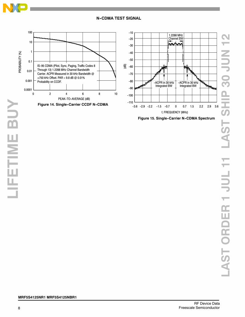
N--CDMA TEST SIGNAL
100.0001
100
0
PEAK--TO--AVERAGE (dB)
Figure 14. Single--Carrier CCDF N--CDMA
10
1
0.1
0.01
0.001
2 4 6 8
IS--95 CDMA (Pilot, Sync, Paging, Traffic Codes 8Through 13) 1.2288 MHz Channel BandwidthCarrier. ACPR Measured in 30 kHz Bandwidth @±750 kHz Offset. PAR = 9.8 dB @ 0.01%Probability on CCDF.
PROBABILITY
(%)
--60
--110
--10
(dB)
--20
--30
--40
--50
--70
--80
--90
--100
1.2288 MHzChannel BW
2.90.7 2.21.50--0.7--1.5--2.2--2.9--3.6 3.6
f, FREQUENCY (MHz)
Figure 15. Single--Carrier N--CDMA Spectrum
--ACPR in 30 kHzIntegrated BW
--ACPR in 30 kHzIntegrated BW
LIFETIMEBUY
LASTORDER1JU
L11
LASTSHIP
30JU
N12
MRF5S4125NR1 MRF5S4125NBR1
9RF Device DataFreescale Semiconductor
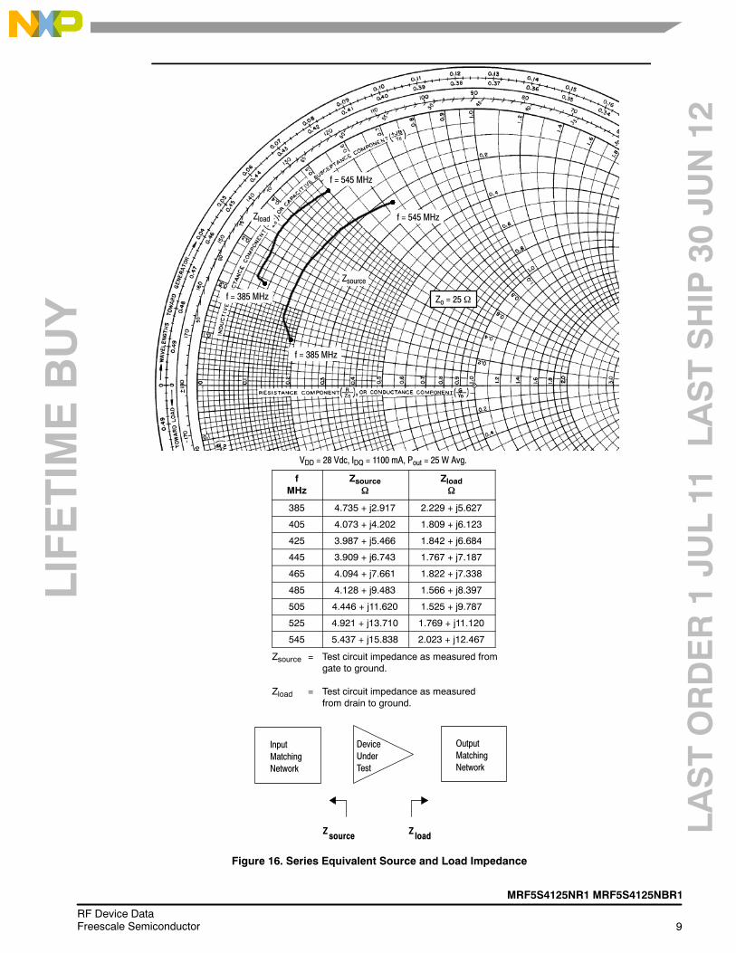
Zo = 25Ω
Zload
Zsource
f = 385 MHz
f = 545 MHz
f = 545 MHz
f = 385 MHz
VDD = 28 Vdc, IDQ = 1100 mA, Pout = 25 W Avg.
fMHz
ZsourceΩ
ZloadΩ
385 4.735 + j2.917 2.229 + j5.627
405 4.073 + j4.202 1.809 + j6.123
425 3.987 + j5.466 1.842 + j6.684
445 3.909 + j6.743 1.767 + j7.187
465 4.094 + j7.661 1.822 + j7.338
485 4.128 + j9.483 1.566 + j8.397
505 4.446 + j11.620 1.525 + j9.787
525 4.921 + j13.710 1.769 + j11.120
545 5.437 + j15.838 2.023 + j12.467
Zsource = Test circuit impedance as measured fromgate to ground.
Zload = Test circuit impedance as measuredfrom drain to ground.
Figure 16. Series Equivalent Source and Load Impedance
Zsource Z load
InputMatchingNetwork
DeviceUnderTest
OutputMatchingNetwork
LIFETIMEBUY
LASTORDER1JU
L11
LASTSHIP
30JU
N12
10RF Device Data
Freescale Semiconductor
MRF5S4125NR1 MRF5S4125NBR1
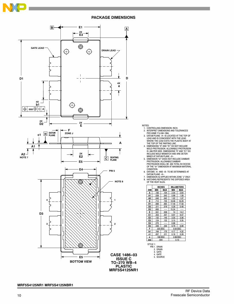
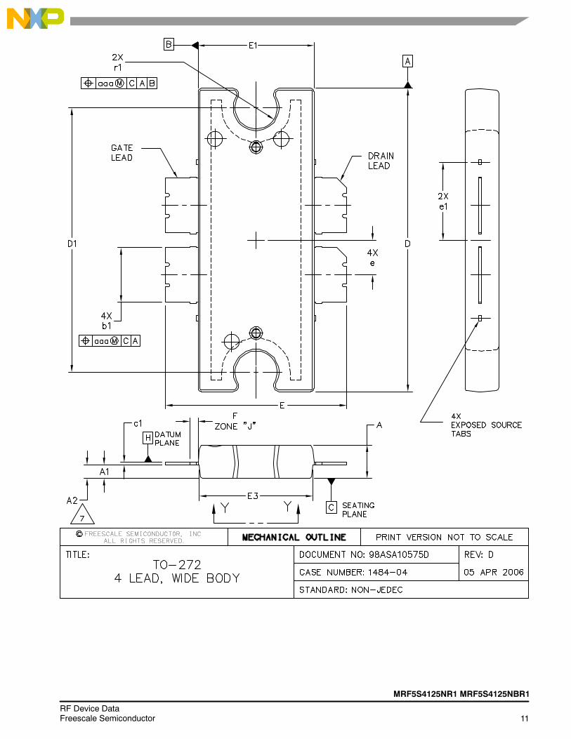
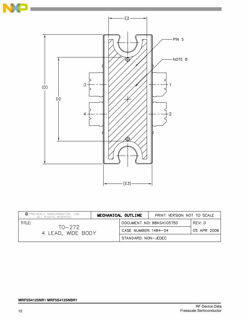
PACKAGE DIMENSIONS
DATUMPLANE
BOTTOM VIEW
A1
2X
D1
E3
E1
D3
E4
A2
PIN 5
NOTE 8
AB
C
H
DRAIN LEAD
D
AMaaa C
4Xb1
2XD2
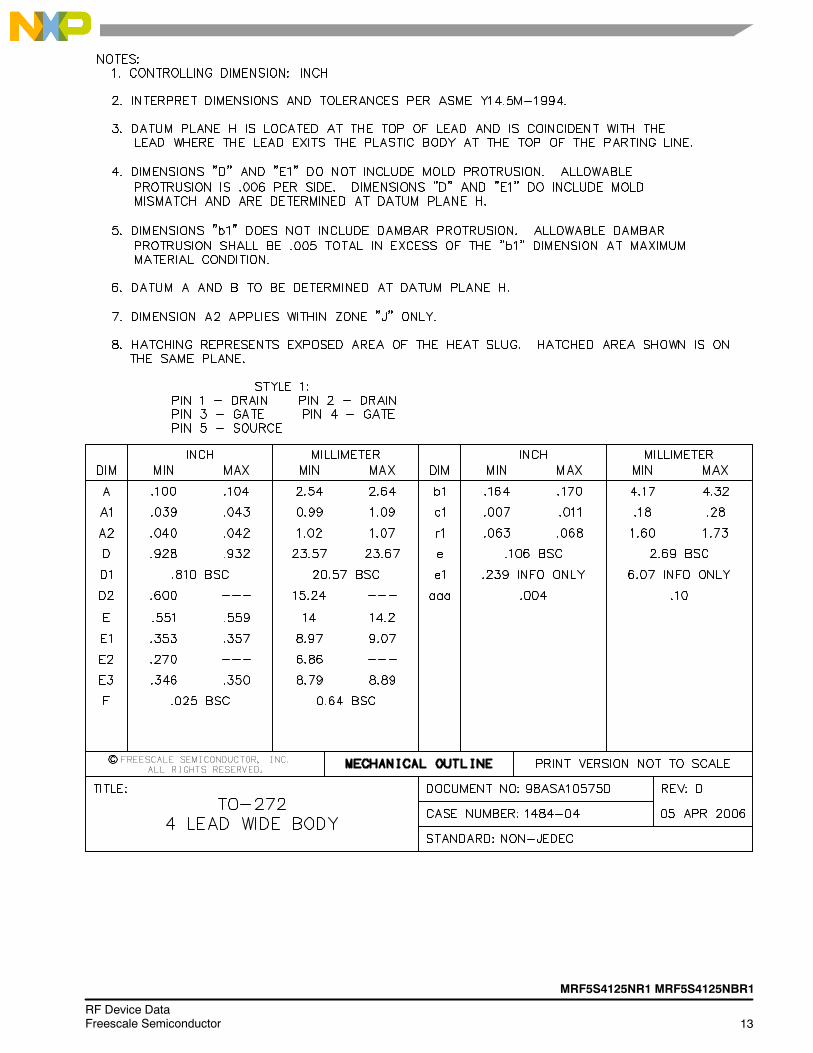
NOTES:1. CONTROLLING DIMENSION: INCH.2. INTERPRET DIMENSIONS AND TOLERANCES
PER ASME Y14.5M--1994.3. DATUM PLANE --H-- IS LOCATED AT THE TOP OF
LEAD AND IS COINCIDENT WITH THE LEADWHERE THE LEAD EXITS THE PLASTIC BODY ATTHE TOP OF THE PARTING LINE.
4. DIMENSIONS D AND E1 DO NOT INCLUDEMOLD PROTRUSION. ALLOWABLE PROTRUSIONIS .006 PER SIDE. DIMENSIONS D AND E1 DOINCLUDE MOLD MISMATCH AND ARE DETER-MINED AT DATUM PLANE --H--.
5. DIMENSION b1 DOES NOT INCLUDE DAMBARPROTRUSION. ALLOWABLE DAMBARPROTRUSION SHALL BE .005 TOTAL IN EXCESSOF THE b1 DIMENSION AT MAXIMUM MATERIALCONDITION.
6. DATUMS --A-- AND --B-- TO BE DETERMINED ATDATUM PLANE --H--.
7. DIMENSION A2 APPLIES WITHIN ZONE J ONLY.8. HATCHING REPRESENTS THE EXPOSED AREA
OF THE HEAT SLUG.
c1F
ZONE J
E22X
A
DIMA
MIN MAX MIN MAXMILLIMETERS
.100 .104 2.54 2.64
INCHES
A1 .039 .043 0.99 1.09A2 .040 .042 1.02 1.07D .712 .720 18.08 18.29D1 .688 .692 17.48 17.58D2 .011 .019 0.28 0.48D3 .600 ------ 15.24 ------E .551 .559 14 14.2E1 .353 .357 8.97 9.07E2 .132 .140 3.35 3.56E3 .124 .132 3.15 3.35E4 .270 ------ 6.86 ------
Fb1 .164 .170 4.17 4.32c1 .007 .011 0.18 0.28e
.025 BSC
.106 BSC
0.64 BSC
2.69 BSC
1
STYLE 1:PIN 1. DRAIN
2. DRAIN3. GATE4. GATE5. SOURCE
aaa .004 0.10
GATE LEAD
4Xe
2XE
SEATINGPLANE
4
23
NOTE 7
E5
E5
E5 .346 .350 8.79 8.89
CASE 1486--03ISSUE C
TO--270 WB--4PLASTIC
MRF5S4125NR1
MRF5S4125NR1 MRF5S4125NBR1
11RF Device DataFreescale Semiconductor
12RF Device Data
Freescale Semiconductor
MRF5S4125NR1 MRF5S4125NBR1
MRF5S4125NR1 MRF5S4125NBR1
13RF Device DataFreescale Semiconductor
14RF Device Data
Freescale Semiconductor
MRF5S4125NR1 MRF5S4125NBR1
PRODUCT DOCUMENTATION
Refer to the following documents to aid your design process.
Application Notes• AN1907: Solder Reflow Attach Method for High Power RF Devices in Plastic Packages
• AN1955: Thermal Measurement Methodology of RF Power Amplifiers
• AN3263: Bolt Down Mounting Method for High Power RF Transistors and RFICs in Over--Molded Plastic Packages
Engineering Bulletins• EB212: Using Data Sheet Impedances for RF LDMOS Devices
REVISION HISTORY
The following table summarizes revisions to this document.
Revision Date Description
0 Jan. 2007 • Initial Release of Data Sheet
LIFETIMEBUY
LASTORDER1JU
L11
LASTSHIP
30JU
N12
MRF5S4125NR1 MRF5S4125NBR1
15RF Device DataFreescale Semiconductor
Information in this document is provided solely to enable system and softwareimplementers to use Freescale Semiconductor products. There are no express orimplied copyright licenses granted hereunder to design or fabricate any integratedcircuits or integrated circuits based on the information in this document.
Freescale Semiconductor reserves the right to make changes without further notice toany products herein. Freescale Semiconductor makes no warranty, representation orguarantee regarding the suitability of its products for any particular purpose, nor doesFreescale Semiconductor assume any liability arising out of the application or use ofany product or circuit, and specifically disclaims any and all liability, including withoutlimitation consequential or incidental damages. Typical parameters that may beprovided in Freescale Semiconductor data sheets and/or specifications can and dovary in different applications and actual performance may vary over time. All operatingparameters, including Typicals, must be validated for each customer application bycustomers technical experts. Freescale Semiconductor does not convey any licenseunder its patent rights nor the rights of others. Freescale Semiconductor products arenot designed, intended, or authorized for use as components in systems intended forsurgical implant into the body, or other applications intended to support or sustain life,or for any other application in which the failure of the Freescale Semiconductor productcould create a situation where personal injury or death may occur. Should Buyerpurchase or use Freescale Semiconductor products for any such unintended orunauthorized application, Buyer shall indemnify and hold Freescale Semiconductorand its officers, employees, subsidiaries, affiliates, and distributors harmless against allclaims, costs, damages, and expenses, and reasonable attorney fees arising out of,directly or indirectly, any claim of personal injury or death associated with suchunintended or unauthorized use, even if such claim alleges that FreescaleSemiconductor was negligent regarding the design or manufacture of the part.
Freescalet and the Freescale logo are trademarks of Freescale Semiconductor, Inc.All other product or service names are the property of their respective owners.© Freescale Semiconductor, Inc. 2007. All rights reserved.
How to Reach Us:
Home Page:www.freescale.com
Web Support:http://www.freescale.com/support
USA/Europe or Locations Not Listed:Freescale Semiconductor, Inc.Technical Information Center, EL5162100 East Elliot RoadTempe, Arizona 85284+1--800--521--6274 or +1--480--768--2130www.freescale.com/support
Europe, Middle East, and Africa:Freescale Halbleiter Deutschland GmbHTechnical Information CenterSchatzbogen 781829 Muenchen, Germany+44 1296 380 456 (English)+46 8 52200080 (English)+49 89 92103 559 (German)+33 1 69 35 48 48 (French)www.freescale.com/support
Japan:Freescale Semiconductor Japan Ltd.HeadquartersARCO Tower 15F1--8--1, Shimo--Meguro, Meguro--ku,Tokyo 153--0064Japan0120 191014 or +81 3 5437 [email protected]
Asia/Pacific:Freescale Semiconductor Hong Kong Ltd.Technical Information Center2 Dai King StreetTai Po Industrial EstateTai Po, N.T., Hong Kong+800 2666 [email protected]
For Literature Requests Only:Freescale Semiconductor Literature Distribution CenterP.O. Box 5405Denver, Colorado 802171--800--441--2447 or 303--675--2140Fax: [email protected]
Document Number: MRF5S4125NRev. 0, 1/2007
Related Documents