Field Effect Transistor By Mr. Aniket Kumar Assistant Professor, Department of Electronics & Communication Engineering Shobhit Institute of Engineering & Technology (Deemed to-be University) NH-58, Modipuram, Meerut – 250 110, India

Welcome message from author
This document is posted to help you gain knowledge. Please leave a comment to let me know what you think about it! Share it to your friends and learn new things together.
Transcript

Field Effect Transistor By
Mr. Aniket Kumar Assistant Professor, Department of Electronics & Communication Engineering
Shobhit Institute of Engineering & Technology (Deemed to-be University) NH-58, Modipuram, Meerut – 250 110, India
Chapter-7 Field Effect transistor
JFET The junction FET, abbreviated as JFET has three terminals a source , gate & drain . The JFET has two diodes: the gate-source diode and the gate-drain diode. For normal operation , the gate –source diode is reverse biased; then , the gate voltage controls the drain current. Drain Curves Maximum drain current occurs when the gate-source voltage is zero. The pinchoff voltage separates the ohmic and active regions for VGS =0 . The gate-source cutoff voltage has the same magnitude as the pinchoff voltage. VGS(off) turns the JFET off. Biasing in the Ohmic region Gate bias is used to bias a JFET in the ohmic region. When it operates in the ohmic region , a JFET is equivalent to a small resistance of RDS. To ensure operation in the ohmic region , the JFET is driven into hard saturation by using VGS= 0 and ID(sat)<< IDSS Biasing in the active region When the gate voltage is much larger than VGS, voltage divider bias can set up a stable Q point in the active region. When +ve & -ve supply voltages are available , two –supply source bias can used to get a stable Q point. Self-bias is used only with small-signal amplifiers because the Q point is less stable than with the other biasing methods. Transconductance Transconductance gm tells us how effective the gate voltage is in controlling the drain current. The quantity gm is the slope of the transconductance curve, which increases as VGS approaches zero. The Transconductance curve This is a graph of drain current versus gate-source voltage. The drain current increases more rapidly as VGS approaches zero. Because the equation for drain current contains a squared quantity, JFETs are referred to as square-law devices. The normalized transconductance curve shows that ID equals one-quarter of maximum when VGS equal half of cutoff. JFET Amplifier A CS amplifier has a voltage gain of gmr’d and produces an inverted output signal. One of the most important uses of a JFET amplifier is the source follower, which is often used at the front end of systems because of its high input resistance. The JFET Analog Switch JFET acts like a switch that either transmits or blocks a small ac signal. To get this type of action , the JFET is biased into hard saturation or cutoff, depending on whether VGS is high or low. JFET shunt and series switches are used. The series type has a higher on-off ratio. MOSFET The metal–oxide–semiconductor field-effect transistor (MOSFET, MOS-FET, or MOS FET) is a type of field-effect transistor (FET). It has an insulated gate, whose voltage determines the conductivity of the device. This ability to change conductivity with the amount of applied voltage can be used for amplifying or switching electronic signals. The D- MOSFET The depletion mode MOSFET , abbreviated as D- MOSFET is normally on, has a source , gate and drain. The gate is insulated from the channel. Because of this, the input resistance is very high. The D-MOSFET has limited use, mainly in RF circuits. The E- MOSFET The Enhancement mode MOSFET is abbreviated as E- MOSFET is normally off. When the gate voltage equals the threshold voltage, an n-type inversion layers connects the source to the drain. When the gate voltage is much greater than the threshold voltage , the device conducts heavily.
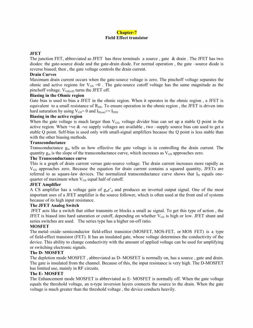
MOSFET Preamplifier MOSFET is an amplifying device in which the output current depends on the input voltage. The MOSFET Pre Amplifier is a sensitive and stable Preamp circuit using an N-Channel MOSFET and a PNP Bipolar transistor. This combination gives high input impedance and low output impedance with stabilized gain. MOSFET Uses The MOSFET (Metal Oxide Semiconductor Field Effect Transistor) transistor is a semiconductor device which is widely used for switching and amplifying electronic signals in the electronic devices. The MOSFET is very far the most common transistor and can be used in both analog and digital ckt. MOSFET used in various electrical and electronic projects which are designed by using various electrical and electronic components. CMOS CMOS uses two complementary MOSFETs, in which one conducts and the other shuts off. The CMOS inverter is a basic digital circuit, CMOS device have the advantage of very low power consumption. Definitions Ohmic resistance at pinchoff Hard Saturation
RDS = VP/ IDSS ID(sat)<< IDSS
Transconductance Ohmic resistance near origin
gm= id/VGS rds= VDS/iD
D-MOSFET drain current On resistance
ID=IDSS(1- VGS/ VGS(off))2
RDS(on)=VDS(on)/ ID(on)
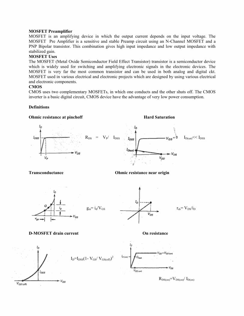
Derivations : Gate-source cutoff voltage : Drain current
VGS(off)= -VP ID=IDSS(1-VGS/VGS(off))
Gate cutoff voltage Self bias
VGS(off)= -2IDSS/gm0 VGS= -IDRS
Voltage divider bias Source bias ID= (VG-VGS)/RS ≈ VG /RS ID = (VSS-VGS)/RS≈ VSS /RS
Ohmic region
ID(sat)< ID(on)
Long & Short Questions Q.1. Explain with proper diagram the construction and working of an n-channel JFET. Draw
and explain necessary circuit diagram to obtain its characteristics. Or
With the help of neat sketches and characteristics curve explain the junction FET.
Or
What are the different types of field effect transistor ? Draw drain and output characteristics of a field effect transistor .
Or Explain pinch-off voltage and draw drain characteristics of FET and also show the parameters of FET and relation between them.
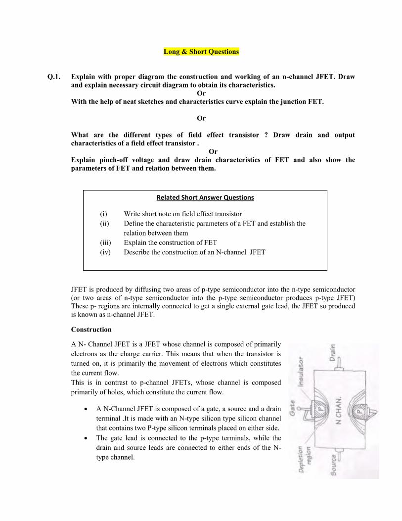
JFET is produced by diffusing two areas of p-type semiconductor into the n-type semiconductor (or two areas of n-type semiconductor into the p-type semiconductor produces p-type JFET) These p- regions are internally connected to get a single external gate lead, the JFET so produced is known as n-channel JFET.
Construction
A N- Channel JFET is a JFET whose channel is composed of primarily electrons as the charge carrier. This means that when the transistor is turned on, it is primarily the movement of electrons which constitutes the current flow. This is in contrast to p-channel JFETs, whose channel is composed primarily of holes, which constitute the current flow.
A N-Channel JFET is composed of a gate, a source and a drain terminal .It is made with an N-type silicon type silicon channel that contains two P-type silicon terminals placed on either side.
The gate lead is connected to the p-type terminals, while the drain and source leads are connected to either ends of the N-type channel.
Related Short Answer Questions
(i) Write short note on field effect transistor (ii) Define the characteristic parameters of a FET and establish the
relation between them (iii) Explain the construction of FET (iv) Describe the construction of an N-channel JFET
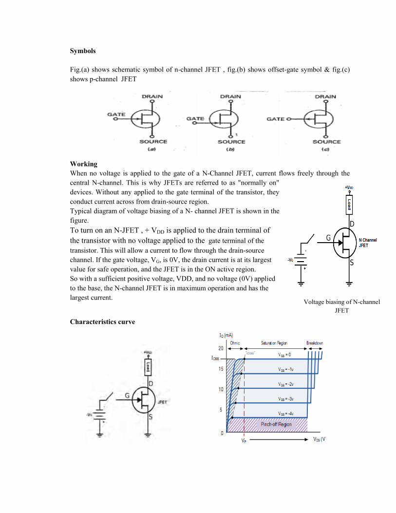
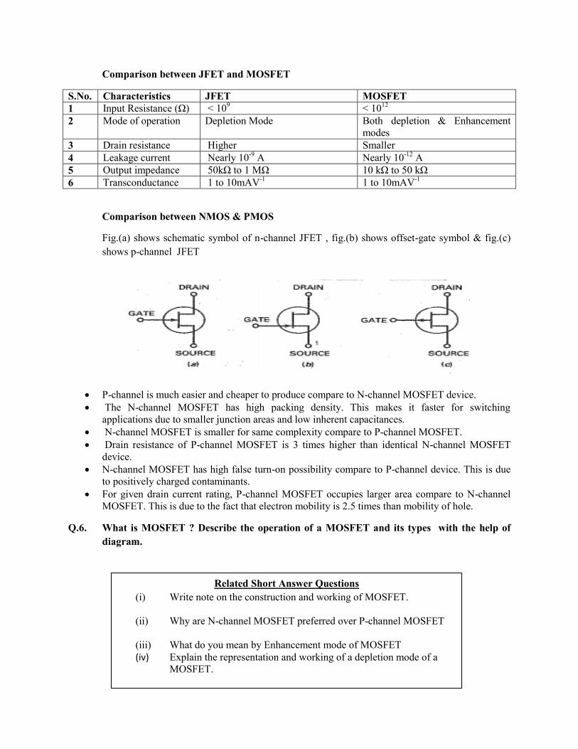
Symbols Fig.(a) shows schematic symbol of n-channel JFET , fig.(b) shows offset-gate symbol & fig.(c) shows p-channel JFET Working When no voltage is applied to the gate of a N-Channel JFET, current flows freely through the central N-channel. This is why JFETs are referred to as "normally on" devices. Without any applied to the gate terminal of the transistor, they conduct current across from drain-source region. Typical diagram of voltage biasing of a N- channel JFET is shown in the figure. To turn on an N-JFET , + VDD is applied to the drain terminal of the transistor with no voltage applied to the gate terminal of the transistor. This will allow a current to flow through the drain-source channel. If the gate voltage, VG, is 0V, the drain current is at its largest value for safe operation, and the JFET is in the ON active region. So with a sufficient positive voltage, VDD, and no voltage (0V) applied to the base, the N-channel JFET is in maximum operation and has the largest current.
Characteristics curve
Voltage biasing of N-channel JFET
The voltage VGS applied to the gate controls the current flowing between the drain and the source terminals. VGS refers to the voltage applied between the gate and the source while VDS refers to the voltage applied between the drain and the source.
The characteristics curves shown above, shows the four different regions of operation for a JFET and these are given as: Ohmic Region : When VGS = 0 the depletion layer of the channel is very small and the JFET acts like a voltage controlled resistor. Cut-off Region : This is also known as the pinch-off region were the Gate voltage, VGS is sufficient to cause the JFET to act as an open circuit as the channel resistance is at maximum. Saturation or Active Region : The JFET becomes a good conductor and is controlled by the Gate-Source voltage, ( VGS ) while the Drain-Source voltage, ( VDS ) has little or no effect.
Breakdown Region : The voltage between the Drain and the Source, ( VDS ) is high enough to causes the JFET’s resistive channel to break down and pass uncontrolled maximum current
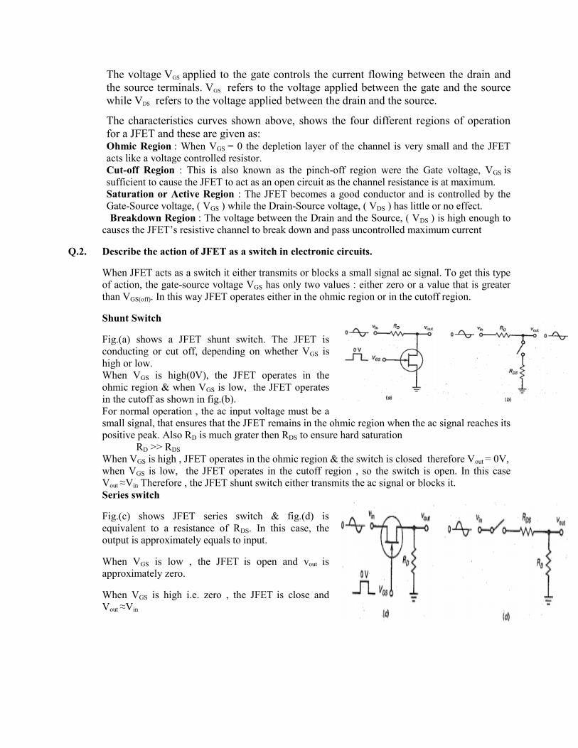
Q.2. Describe the action of JFET as a switch in electronic circuits.
When JFET acts as a switch it either transmits or blocks a small signal ac signal. To get this type of action, the gate-source voltage VGS has only two values : either zero or a value that is greater than VGS(off). In this way JFET operates either in the ohmic region or in the cutoff region.
Shunt Switch
Fig.(a) shows a JFET shunt switch. The JFET is conducting or cut off, depending on whether VGS is high or low. When VGS is high(0V), the JFET operates in the ohmic region & when VGS is low, the JFET operates in the cutoff as shown in fig.(b). For normal operation , the ac input voltage must be a small signal, that ensures that the JFET remains in the ohmic region when the ac signal reaches its positive peak. Also RD is much grater then RDS to ensure hard saturation RD >> RDS When VGS is high , JFET operates in the ohmic region & the switch is closed therefore Vout = 0V, when VGS is low, the JFET operates in the cutoff region , so the switch is open. In this case Vout ≈Vin Therefore , the JFET shunt switch either transmits the ac signal or blocks it. Series switch
Fig.(c) shows JFET series switch & fig.(d) is equivalent to a resistance of RDS. In this case, the output is approximately equals to input.
When VGS is low , the JFET is open and vout is approximately zero.
When VGS is high i.e. zero , the JFET is close and Vout ≈Vin
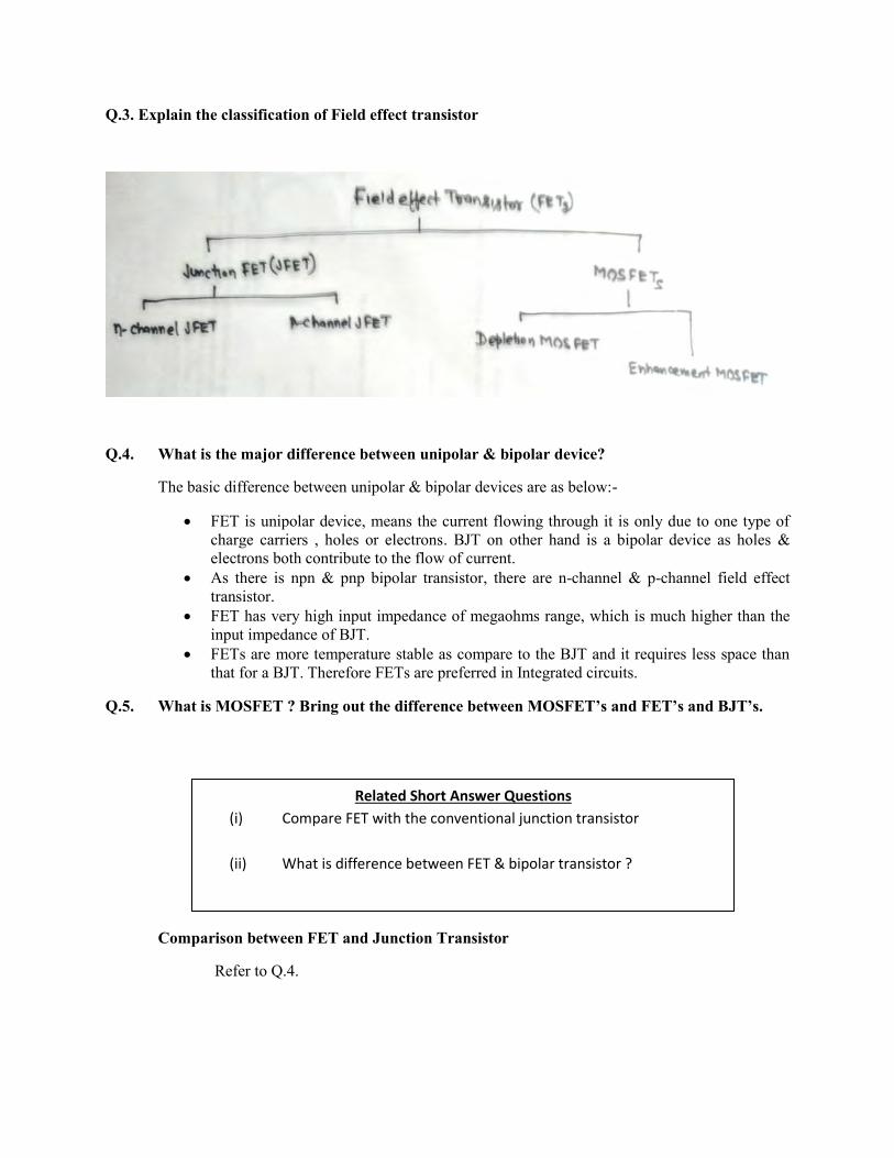
Q.3. Explain the classification of Field effect transistor
Q.4. What is the major difference between unipolar & bipolar device?
The basic difference between unipolar & bipolar devices are as below:-
FET is unipolar device, means the current flowing through it is only due to one type of charge carriers , holes or electrons. BJT on other hand is a bipolar device as holes & electrons both contribute to the flow of current.
As there is npn & pnp bipolar transistor, there are n-channel & p-channel field effect transistor.
FET has very high input impedance of megaohms range, which is much higher than the input impedance of BJT.
FETs are more temperature stable as compare to the BJT and it requires less space than that for a BJT. Therefore FETs are preferred in Integrated circuits.
Q.5. What is MOSFET ? Bring out the difference between MOSFET’s and FET’s and BJT’s.
Comparison between FET and Junction Transistor
Refer to Q.4.
Related Short Answer Questions
(i) Compare FET with the conventional junction transistor
(ii) What is difference between FET & bipolar transistor ?
Comparison between JFET and MOSFET
S.No. Characteristics JFET MOSFET 1 Input Resistance (Ω) < 109 < 1012 2 Mode of operation Depletion Mode Both depletion & Enhancement
modes 3 Drain resistance Higher Smaller 4 Leakage current Nearly 10-9 A Nearly 10-12 A 5 Output impedance 50kΩ to 1 MΩ 10 kΩ to 50 kΩ 6 Transconductance 1 to 10mAV-1 1 to 10mAV-1
Comparison between NMOS & PMOS
Fig.(a) shows schematic symbol of n-channel JFET , fig.(b) shows offset-gate symbol & fig.(c) shows p-channel JFET
P-channel is much easier and cheaper to produce compare to N-channel MOSFET device. The N-channel MOSFET has high packing density. This makes it faster for switching
applications due to smaller junction areas and low inherent capacitances. N-channel MOSFET is smaller for same complexity compare to P-channel MOSFET. Drain resistance of P-channel MOSFET is 3 times higher than identical N-channel MOSFET
device. N-channel MOSFET has high false turn-on possibility compare to P-channel device. This is due
to positively charged contaminants. For given drain current rating, P-channel MOSFET occupies larger area compare to N-channel
MOSFET. This is due to the fact that electron mobility is 2.5 times than mobility of hole.
Q.6. What is MOSFET ? Describe the operation of a MOSFET and its types with the help of diagram.
Related Short Answer Questions (i) Write note on the construction and working of MOSFET.
(ii) Why are N-channel MOSFET preferred over P-channel MOSFET
(iii) What do you mean by Enhancement mode of MOSFET (iv) Explain the representation and working of a depletion mode of a
MOSFET.
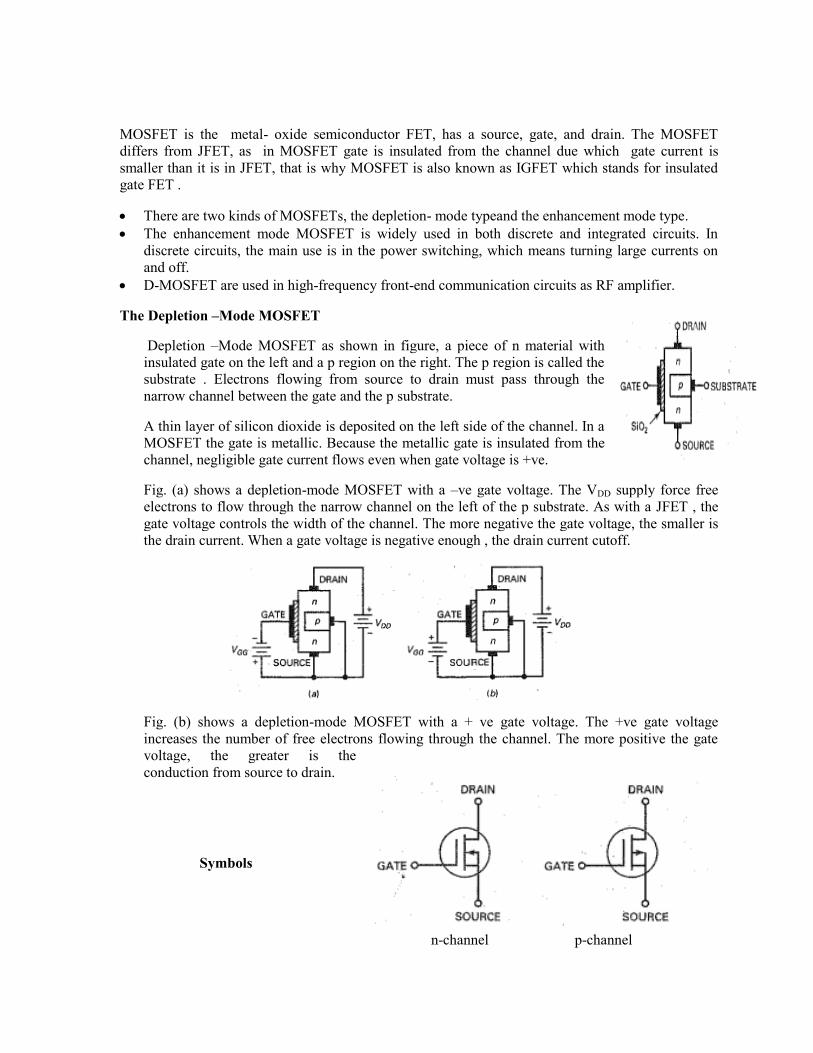
MOSFET is the metal- oxide semiconductor FET, has a source, gate, and drain. The MOSFET differs from JFET, as in MOSFET gate is insulated from the channel due which gate current is smaller than it is in JFET, that is why MOSFET is also known as IGFET which stands for insulated gate FET .
There are two kinds of MOSFETs, the depletion- mode typeand the enhancement mode type. The enhancement mode MOSFET is widely used in both discrete and integrated circuits. In
discrete circuits, the main use is in the power switching, which means turning large currents on and off.
D-MOSFET are used in high-frequency front-end communication circuits as RF amplifier.
The Depletion –Mode MOSFET
Depletion –Mode MOSFET as shown in figure, a piece of n material with insulated gate on the left and a p region on the right. The p region is called the substrate . Electrons flowing from source to drain must pass through the narrow channel between the gate and the p substrate.
A thin layer of silicon dioxide is deposited on the left side of the channel. In a MOSFET the gate is metallic. Because the metallic gate is insulated from the channel, negligible gate current flows even when gate voltage is +ve.
Fig. (a) shows a depletion-mode MOSFET with a –ve gate voltage. The VDD supply force free electrons to flow through the narrow channel on the left of the p substrate. As with a JFET , the gate voltage controls the width of the channel. The more negative the gate voltage, the smaller is the drain current. When a gate voltage is negative enough , the drain current cutoff.
Fig. (b) shows a depletion-mode MOSFET with a + ve gate voltage. The +ve gate voltage increases the number of free electrons flowing through the channel. The more positive the gate voltage, the greater is the conduction from source to drain.
Symbols
n-channel p-channel
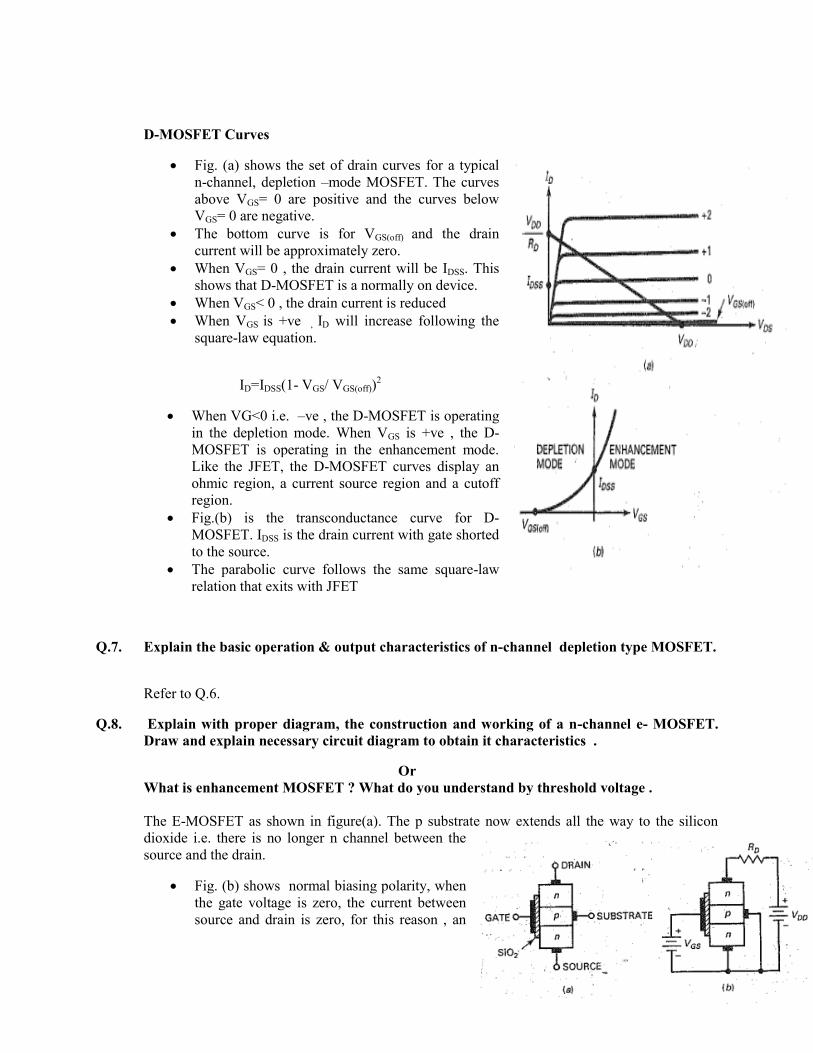
D-MOSFET Curves
Fig. (a) shows the set of drain curves for a typical n-channel, depletion –mode MOSFET. The curves above VGS= 0 are positive and the curves below VGS= 0 are negative.
The bottom curve is for VGS(off) and the drain current will be approximately zero.
When VGS= 0 , the drain current will be IDSS. This shows that D-MOSFET is a normally on device.
When VGS< 0 , the drain current is reduced When VGS is +ve , ID will increase following the
square-law equation.
ID=IDSS(1- VGS/ VGS(off))2
When VG<0 i.e. –ve , the D-MOSFET is operating in the depletion mode. When VGS is +ve , the D-MOSFET is operating in the enhancement mode. Like the JFET, the D-MOSFET curves display an ohmic region, a current source region and a cutoff region.
Fig.(b) is the transconductance curve for D-MOSFET. IDSS is the drain current with gate shorted to the source.
The parabolic curve follows the same square-law relation that exits with JFET
Q.7. Explain the basic operation & output characteristics of n-channel depletion type MOSFET.
Refer to Q.6.
Q.8. Explain with proper diagram, the construction and working of a n-channel e- MOSFET. Draw and explain necessary circuit diagram to obtain it characteristics .
Or What is enhancement MOSFET ? What do you understand by threshold voltage . The E-MOSFET as shown in figure(a). The p substrate now extends all the way to the silicon
dioxide i.e. there is no longer n channel between the source and the drain.
Fig. (b) shows normal biasing polarity, when the gate voltage is zero, the current between source and drain is zero, for this reason , an
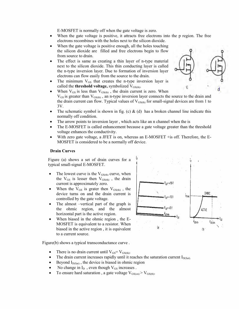
E-MOSFET is normally off when the gate voltage is zero. When the gate voltage is positive, it attracts free electrons into the p region. The free
electrons recombines with the holes next to the silicon dioxide. When the gate voltage is positive enough, all the holes touching
the silicon dioxide are filled and free electrons begin to flow from source to drain.
The effect is same as creating a thin layer of n-type material next to the silicon dioxide. This thin conducting layer is called the n-type inversion layer. Due to formation of inversion layer electrons can flow easily from the source to the drain.
The minimum VGS that creates the n-type inversion layer is called the threshold voltage, symbolized VGS(th).
When VGS is less than VGS(th) , the drain current is zero. When VGS is greater than VGS(th) , an n-type inversion layer connects the source to the drain and the drain current can flow. Typical values of VGS(th) for small-signal devices are from 1 to 3V.
The schematic symbol is shown in fig. (c) & (d) has a broken channel line indicate this normally off condition.
The arrow points to inversion layer , which acts like an n channel when the is The E-MOSFET is called enhancement because a gate voltage greater than the threshold
voltage enhances the conductivity. With zero gate voltage, a JFET is on, whereas an E-MOSFET +is off. Therefore, the E-
MOSFET is considered to be a normally off device.
Drain Curves
Figure (a) shows a set of drain curves for a typical small-signal E-MOSFET.
The lowest curve is the VGS(th) curve, when the VGS is lesser then VGS(th) , the drain current is approximately zero.
When the VGS is grater then VGS(th) , the device turns on and the drain current is controlled by the gate voltage.
The almost –vertical part of the graph is the ohmic region, and the almost horizontal part is the active region.
When biased in the ohmic region , the E-MOSFET is equivalent to a resistor. When biased in the active region , it is equivalent to a current source.
Figure(b) shows a typical transconductance curve .
There is no drain current until VGS= VGS(th). The drain current increases rapidly until it reaches the saturation current ID(Sat). Beyond ID(Sat) , the device is biased in ohmic region No change in ID , even though VGS increases . To ensure hard saturation , a gate voltage VGS(on) > VGS(th).
Q.9. Explain how output characteristics of a MOSFET are obtained . Illustrate with proper electronic circuits. Draw output characteristics of depletion type & enhancement type MOSFET and explain the difference between them.
Ref. to Q.6. & Q.8.
Difference between depletion type & enhancement type MOSFET
1. Enhancement type mode MOSFET will be off for gate to source voltage 0V as there exists no channel to conduct. Depletion type MOSFET conducts at 0V has positive cut off gate voltage so less preferred. Depletion MOS also conducts at 0V therefore has less useful application.
2. Since the logic operations of depletion MOSFET is the opposite to the enhancement MOSFET, the depletion MOSFET produces positive logic circuits, such as, buffer, AND, and OR.
3. Diffusion current (i.e. sub-threshold leakage current) exists in enhancement MOSFET while depletion MOSFET do not have any diffusion current.
4. As a enhancement MOSFET shrinking in size, there is no way to stop the sub threshold leakage current diffused across from source to drain because the drain and source terminals are closer physically. This is not the problem with depletion type MOSFET because a pinched channel stops the diffusion current completely.
5. Depletion MOSFET logic operations are opposite to enhancement type of MOSFETs.
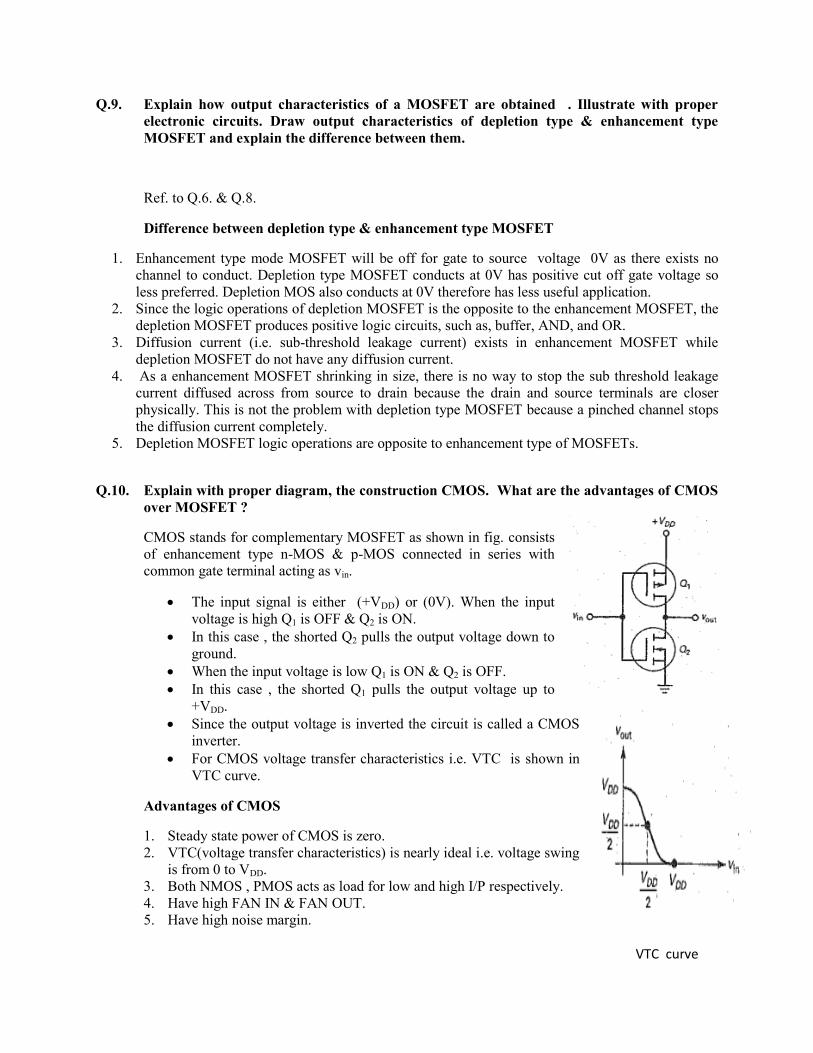
Q.10. Explain with proper diagram, the construction CMOS. What are the advantages of CMOS over MOSFET ?
CMOS stands for complementary MOSFET as shown in fig. consists of enhancement type n-MOS & p-MOS connected in series with common gate terminal acting as vin.
The input signal is either (+VDD) or (0V). When the input voltage is high Q1 is OFF & Q2 is ON.
In this case , the shorted Q2 pulls the output voltage down to ground.
When the input voltage is low Q1 is ON & Q2 is OFF. In this case , the shorted Q1 pulls the output voltage up to
+VDD. Since the output voltage is inverted the circuit is called a CMOS
inverter. For CMOS voltage transfer characteristics i.e. VTC is shown in
VTC curve.
Advantages of CMOS
1. Steady state power of CMOS is zero. 2. VTC(voltage transfer characteristics) is nearly ideal i.e. voltage swing
is from 0 to VDD. 3. Both NMOS , PMOS acts as load for low and high I/P respectively. 4. Have high FAN IN & FAN OUT. 5. Have high noise margin.
VTC curve
Numerical
Q.1. A JFET has VGS(off) =-4V & IDSS= 5mA. What are the gate voltage & drain current at the half cutoff point ? Exp: At half cutoff point VGS= -4V/2 = -2V
∵ ID=IDSS(1- VGS/ VGS(off))2
∴ ID= 5mA(1-2/4)2
= 5mA/4 =1.25mA Ans
Q.2. A JFET has IDSS= 5mA and gm0= 500μS. What is the value of VGS(off)? What does gm equal when VGS = -1V ?
Exp: ∵ gm0= -2 IDSS/ VGS(off)
∴ VGS(off)= -2 IDSS/ gm0
∴ VGS(off) = -2(5mA)/ 500μS = -2V
∵ gm= gm0 (1- VGS/ VGS(off))
∴ gm= (500 μS) (1- 1/2)
= 2500 μS Ans
Q.3. The following readings were obtained in an experiment with FET.
VGS(Volts) VDS(Volts) ID(mA) 0.0 06 12 0.0 16 12.3 0.3 16 12.0 Calculate
(i) AC drain resistance (ii) Transconductance (iii) Amplification Factor
Exp: According to the given reading For constant VGS at 0V
(i) Change in drain to source voltage (ΔVDS) = 16-6 = 10V Change in drain Current (ΔID) = 12.3-12 = 0.3mA ∵ AC drain resistance(rd) = ΔVDS / ΔID at constant VGS
∴ rd = 10V/0.3mA = 33.3kΩ
(ii) Drain current changes from 12.3mA to 12mA and VGS changes from 0.0V to 0.3V at constant VDS that is at 16V.
ΔVGS= 0.3- 0.0 = 0.3V ΔID = 12.3-12 = 0.3mA ∵ Transconductance(gm) = ΔID / ΔVGS at constant VDS ∴ gm = 0.3mA / 0.3V = 0.3m mho
(iii) Amplification Factor (μ) = rd. gm ∴ μ = 33.3kΩ x 0.3m mho = 33.3 Ans
Q.2. The following readings were obtained in an experiment with FET. VGS(Volts) VDS(Volts) ID(mA) 0.0 7 10 0.0 15 10.25 -0.2 15 9.65 Calculate
(i) AC drain resistance (ii) Transconductance (iii) Amplification Factor of JFET
Exp: According to the given reading For constant VGS at 0V (i) Change in drain to source voltage (ΔVDS) = 15-7 = 8V
Change in drain Current (ΔID) = 10.25-10 = 0.25mA ∵ AC drain resistance(rd) = ΔVDS / ΔID at constant VGS
∴ rd = 8V/0.25mA = 32kΩ
(ii) Drain current changes from 10.25mA to 9.65mA and VGS changes from 0.0V to -0.2 at constant VDS that is at 15V.
ΔVGS= -0.2- 0.0 = -0.2V ΔID = 9.65-10.25 = -0.6mA ∵ Transconductance(gm) = ΔID / ΔVGS at constant VDS ∴ gm = -0.6mA / -0.2V = 0.3m mho
(iii) Amplification Factor (μ) = rd. gm ∴ μ = 32kΩ x 0.3m mho = 96 Ans
Q.3. When VGS of a FET changes from -3.1V to -3V the drain current changes from 1mA to
1.3mA. What is the value of transconductance ? Exp: Given ΔVGS= (-3V)-(-3.1V)= 0.1V ΔID = 1.3mA - 1mA= 0.3mA gm = ?
∵ Transconductance(gm) = ΔID / ΔVGS
∴ gm = 0.3mA/ 0.1V = 3m mho Ans Q.4. When gate- source voltage VDS of a FET changes from -3.1V to -2.9V the drain current
changes from 1mA to 1.2mA. What is the value of transconductance ? Exp: Given ΔVGS= (-2.9V)-(-3.1V)= 0.2V ΔID = 1.2mA - 1mA= 0.2mA gm = ?
∵ Transconductance(gm) = ΔID / ΔVGS
∴ gm = 0.2mA/ 0.2V = 1m mho Ans Q.5. An n-channel FET has IDSS =12mA and pinch off voltage VP = -4V . Find drain current for
VGS = -2V , where symbols have their usual meanings. Exp: Given IDSS =12mA, VP = -4V, VGS = -2V , ID = ? ∵ ID=IDSS(1- VGS/ VGS(off))2
∴ ID= 12mA(1-2/4)2 = 6mA Ans
Q.6. An n-channel silicon JFET has a donor concentration of 2x 10²¹/ m3 and a channel width of 4μm , If the dielectric constant of silicon is 12, find the pinch off voltage.
Exp: Given ND = 2x 10²¹/ m3 , Channel width= 4 x10⁻⁶m , ksilicon= 12 VP(pinch off voltage) =? ∵ VP = e ND
2𝜖𝑎2
, Putting the values from given data , we have
∴ VP = e ND
2𝑘𝜖0𝑎2
∴ VP = [1.6x 10-19 x 2x 1021] x4 x10-6/ [2x 12 x 8.86 x 10-12]
= 6.02volt Ans
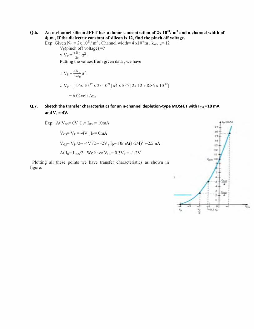
Q.7. Sketch the transfer characteristics for an n-channel depletion-type MOSFET with IDSS =10 mA
and VP =-4V.
Exp: At VGS= 0V , ID= IDSS= 10mA
VGS= VP = -4V , ID= 0mA
VGS= VP /2= -4V /2 = -2V , ID= 10mA(1-2/4)2 =2.5mA
At ID= IDSS/2 , We have VGS= 0.3VP = -1.2V
Plotting all these points we have transfer characteristics as shown in figure.
Related Documents