MP6500 35V, 2.5A, Stepper Motor Driver MP6500 Rev. 1.0 www.MonolithicPower.com 1 6/22/2017 MPS Proprietary Information. Patent Protected. Unauthorized Photocopy and Duplication Prohibited. © 2017 MPS. All Rights Reserved. DESCRIPTION The MP6500 is a stepper motor driver with a built-in translator and current regulation. Current sensing is internal and requires no external sense resistors. High integration and a small package size make the MP6500 a space-saving and cost-effective solution for bipolar stepper motor drives. The MP6500 operates from a supply voltage of up to 35V and can deliver motor currents up to 2.5A (depending on PCB design and thermal conditions). The MP6500 can operate a bipolar stepper motor in full-, half-, quarter-, or eighth- step modes. Internal safety features include over-current protection (OCP), input over- voltage protection (OVP), under-voltage lockout (UVLO), and thermal shutdown. The MP6500 is available in QFN-24 (5mmx5mm) and TSSOP-28 EP packages. FEATURES Wide 4.5V to 35V Input Voltage Range Two Internal Full-Bridge Drivers Internal Current Sensing and Regulation Low On Resistance (HS: 195mΩ, LS: 170mΩ) No Control Power Supply Required Simple Logic Interface 3.3V and 5V Compatible Logic Supply Step Modes from Full-Step to Eighth-Step 2.5A Output Current Automatic Current Decay Over-Current Protection (OCP) Input Over-Voltage Protection (OVP) Thermal Shutdown and Under-Voltage Lockout (UVLO) Protection Fault Indication Output Available in QFN-24 (5mmx5mm) and Thermally Enhanced TSSOP-28 Packages APPLICATIONS Bipolar Stepper Motors Printers All MPS parts are lead-free, halogen-free, and adhere to the RoHS directive. For MPS green status, please visit the MPS website under Quality Assurance. “MPS” and “The Future of Analog IC Technology” are registered trademarks of Monolithic Power Systems, Inc. TYPICAL APPLICATION Step Motor CPA CPB VCP VIN AOUT1 AOUT2 BOUT1 BOUT2 ROSC ISET STEP DIR nENBL MS1 MS2 nSLEEP nFAULT μC VIN MP6500 VG 220 nF 1μF 100nF GND

Welcome message from author
This document is posted to help you gain knowledge. Please leave a comment to let me know what you think about it! Share it to your friends and learn new things together.
Transcript
MP6500 35V, 2.5A, Stepper Motor Driver
MP6500 Rev. 1.0 www.MonolithicPower.com 1
6/22/2017 MPS Proprietary Information. Patent Protected. Unauthorized Photocopy and Duplication Prohibited. © 2017 MPS. All Rights Reserved.
DESCRIPTION The MP6500 is a stepper motor driver with a built-in translator and current regulation. Current sensing is internal and requires no external sense resistors. High integration and a small package size make the MP6500 a space-saving and cost-effective solution for bipolar stepper motor drives.
The MP6500 operates from a supply voltage of up to 35V and can deliver motor currents up to 2.5A (depending on PCB design and thermal conditions). The MP6500 can operate a bipolar stepper motor in full-, half-, quarter-, or eighth-step modes. Internal safety features include over-current protection (OCP), input over-voltage protection (OVP), under-voltage lockout (UVLO), and thermal shutdown.
The MP6500 is available in QFN-24 (5mmx5mm) and TSSOP-28 EP packages.
FEATURES
Wide 4.5V to 35V Input Voltage Range
Two Internal Full-Bridge Drivers
Internal Current Sensing and Regulation
Low On Resistance (HS: 195mΩ, LS: 170mΩ)
No Control Power Supply Required
Simple Logic Interface
3.3V and 5V Compatible Logic Supply
Step Modes from Full-Step to Eighth-Step
2.5A Output Current
Automatic Current Decay
Over-Current Protection (OCP)
Input Over-Voltage Protection (OVP)
Thermal Shutdown and Under-Voltage Lockout (UVLO) Protection
Fault Indication Output
Available in QFN-24 (5mmx5mm) and Thermally Enhanced TSSOP-28 Packages
APPLICATIONS
Bipolar Stepper Motors
Printers
All MPS parts are lead-free, halogen-free, and adhere to the RoHS directive. For MPS green status, please visit the MPS website under Quality Assurance. “MPS” and “The Future of Analog IC Technology” are registered trademarks of Monolithic Power Systems, Inc.
TYPICAL APPLICATION
Step
Motor
CPA
CPB
VCP
VIN
AOUT1
AOUT2
BOUT1
BOUT2
ROSC
ISET
STEP
DIR
nENBL
MS1
MS2
nSLEEP
nFAULT
µC
VIN
MP6500
VG220
nF
1µF
100nF
GND
MP6500 – 35V, 2.5A, STEP MOTOR DRIVER W/ INTERNAL CURRENT SENSE
MP6500 Rev. 1.0 www.MonolithicPower.com 2
6/22/2017 MPS Proprietary Information. Patent Protected. Unauthorized Photocopy and Duplication Prohibited. © 2017 MPS. All Rights Reserved.
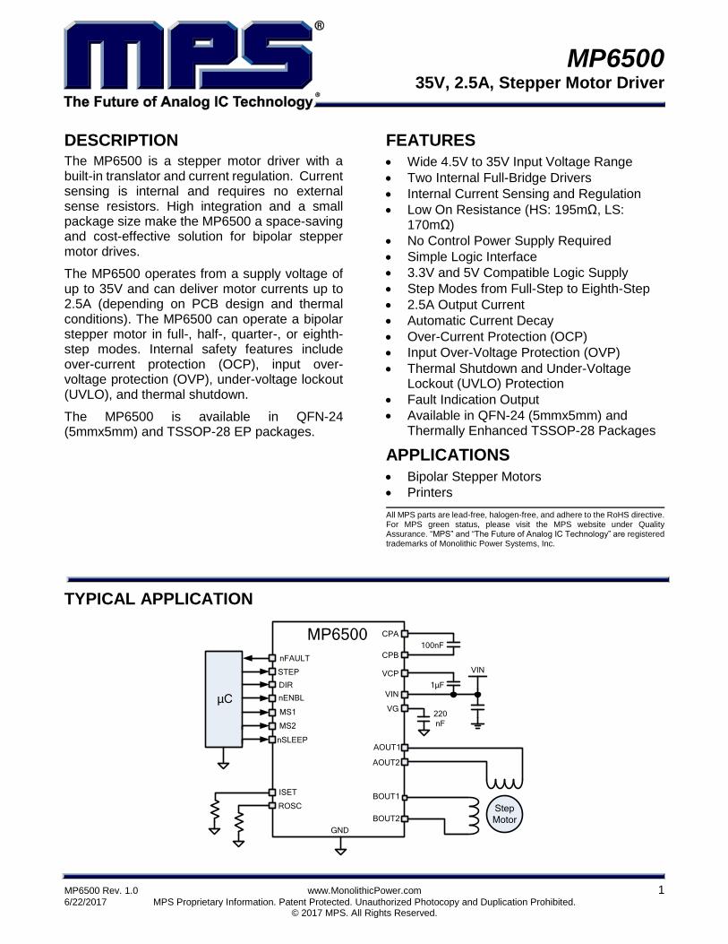
ORDERING INFORMATION
Part Number* Package Top Marking
MP6500GF* TSSOP-28 EP See Below
MP6500GU** QFN-24 (5mmx5mm) See Below
* For Tape & Reel, add suffix –Z (e.g. MP6500GF–Z) ** For Tape & Reel, add suffix –Z (e.g. MP6500GU–Z)
TOP MARKING
MPS: MPS prefix YY: Year code WW: Week code MP6500: Part number LLLLLLLLL: Lot number
TOP MARKING
MPS: MPS prefix YY: Year code WW: Week code MP6500: Part number LLLLLLL: Lot number
PACKAGE REFERENCE
TOP VIEW TOP VIEW
1
3
5
2
4
6
18
16
14
17
15
13
19
21
23
20
22
24
12
108 1197
DIR
nFAULT
ISET
AGND
ROSC
MS2
nENBL
VG
CP1
CP2
VCP
STEP
GN
D
AO
UT
1
VIN
AO
UT
2
GN
D
nS
LE
EP
MS
1
GN
D
BO
UT
1
VIN
BO
UT
2
GN
D
GND
NC
GND
AGND
VIN
BOUT1
MS2
ROSC
CP1 CP2
AOUT1
nFAULT
1
2
3
4
5
6
7
8
9
10
11
12
13
14
28
27
26
25
24
23
22
21
20
19
18
17
16
15
GND
VG
NC
ISET
VIN
GND
nSLEEP
GND
nENBL
BOUT2
GND
STEP
VCP
NC
MS1
NC
AOUT2
DIR
GND
QFN-24 (5mmx5mm) TSSOP-28 EP
MP6500 – 35V, 2.5A, STEP MOTOR DRIVER W/ INTERNAL CURRENT SENSE
MP6500 Rev. 1.0 www.MonolithicPower.com 3
6/22/2017 MPS Proprietary Information. Patent Protected. Unauthorized Photocopy and Duplication Prohibited. © 2017 MPS. All Rights Reserved.
ABSOLUTE MAXIMUM RATINGS (1) Supply voltage (VIN) ...................... -0.3V to 40V xOUTx voltage (VA/BOUT1/2) .............. -0.7V to 40V VCP, CPB .............................. VIN to VIN + 6.5V All other pins to AGND .................. -0.3V to 6.5V ESD rating (HBD) ........................................ 2kV
Continuous power dissipation (TA = +25°C) (2)
QFN ........................................................... 3.5W TSSOP ...................................................... 3.9W Storage temperature ................ -55°C to +150°C Junction temperature ............................. +150°C Lead temperature (solder) ..................... +260°C
Recommended Operating Conditions (3) Supply voltage (VIN) ....................... 4.5V to 35V Output current (IA,BOUT) .............................. ±2.5A Operating junction temp. (TJ). .. -40°C to +125°C
Thermal Resistance (4) θJA θJC QFN-25 (5mmx5mm) ............ 36 ........ 8 .... °C/W TSSOP-28 EP ....................... 32 ........ 6 .... °C/W
NOTES: 1) Exceeding these ratings may damage the device. 2) The maximum allowable power dissipation is a function of the
maximum junction temperature TJ (MAX), the junction-to-ambient thermal resistance θJA, and the ambient temperature TA. The maximum allowable continuous power dissipation at any ambient temperature is calculated by PD (MAX) = (TJ
(MAX)-TA)/θJA. Exceeding the maximum allowable power dissipation produces an excessive die temperature, causing the regulator to go into thermal shutdown. Internal thermal shutdown circuitry protects the device from permanent damage.
3) The device is not guaranteed to function outside of its operating conditions.
4) Measured on JESD51-7, 4-layer PCB.
MP6500 – 35V, 2.5A, STEP MOTOR DRIVER W/ INTERNAL CURRENT SENSE
MP6500 Rev. 1.0 www.MonolithicPower.com 4
6/22/2017 MPS Proprietary Information. Patent Protected. Unauthorized Photocopy and Duplication Prohibited. © 2017 MPS. All Rights Reserved.
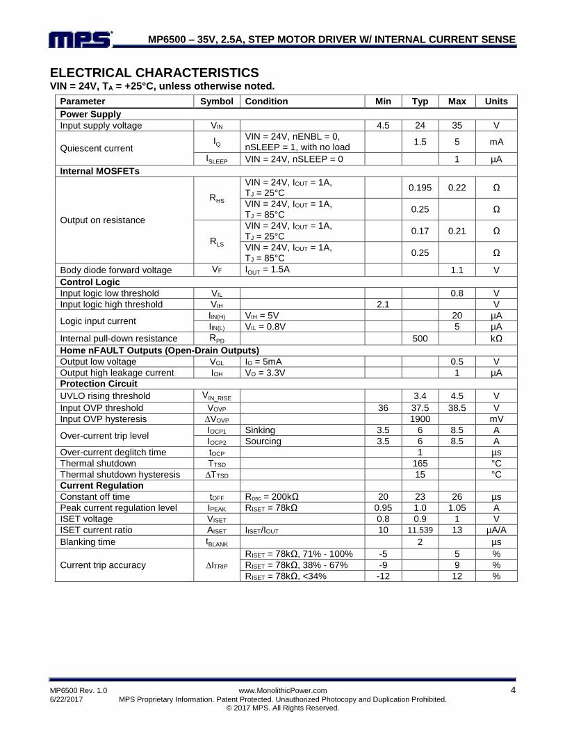
ELECTRICAL CHARACTERISTICS VIN = 24V, TA = +25°C, unless otherwise noted.
Parameter Symbol Condition Min Typ Max Units
Power Supply
Input supply voltage VIN 4.5 24 35 V
Quiescent current IQ
VIN = 24V, nENBL = 0, nSLEEP = 1, with no load
1.5 5 mA
ISLEEP VIN = 24V, nSLEEP = 0 1 µA
Internal MOSFETs
Output on resistance
RHS
VIN = 24V, IOUT = 1A, TJ = 25°C
0.195 0.22 Ω
VIN = 24V, IOUT = 1A, TJ = 85°C
0.25 Ω
RLS
VIN = 24V, IOUT = 1A, TJ = 25°C
0.17 0.21 Ω
VIN = 24V, IOUT = 1A, TJ = 85°C
0.25 Ω
Body diode forward voltage VF IOUT = 1.5A 1.1 V
Control Logic
Input logic low threshold VIL 0.8 V
Input logic high threshold VIH 2.1 V
Logic input current IIN(H) VIH = 5V 20 µA
IIN(L) VIL = 0.8V 5 µA
Internal pull-down resistance RPD 500 kΩ
Home nFAULT Outputs (Open-Drain Outputs)
Output low voltage VOL IO = 5mA 0.5 V
Output high leakage current IOH VO = 3.3V 1 µA
Protection Circuit
UVLO rising threshold VIN_RISE 3.4 4.5 V
Input OVP threshold VOVP 36 37.5 38.5 V
Input OVP hysteresis ∆VOVP 1900 mV
Over-current trip level IOCP1 Sinking 3.5 6 8.5 A
IOCP2 Sourcing 3.5 6 8.5 A
Over-current deglitch time tOCP 1 µs
Thermal shutdown TTSD 165 °C
Thermal shutdown hysteresis ∆TTSD 15 °C
Current Regulation
Constant off time tOFF Rosc = 200kΩ 20 23 26 µs
Peak current regulation level IPEAK RISET = 78kΩ 0.95 1.0 1.05 A
ISET voltage VISET 0.8 0.9 1 V
ISET current ratio AISET IISET/IOUT 10 11.539 13 µA/A
Blanking time tBLANK 2 µs
Current trip accuracy ∆ITRIP
RISET = 78kΩ, 71% - 100% -5 5 %
RISET = 78kΩ, 38% - 67% -9 9 %
RISET = 78kΩ, <34% -12 12 %
MP6500 – 35V, 2.5A, STEP MOTOR DRIVER W/ INTERNAL CURRENT SENSE
MP6500 Rev. 1.0 www.MonolithicPower.com 5
6/22/2017 MPS Proprietary Information. Patent Protected. Unauthorized Photocopy and Duplication Prohibited. © 2017 MPS. All Rights Reserved.
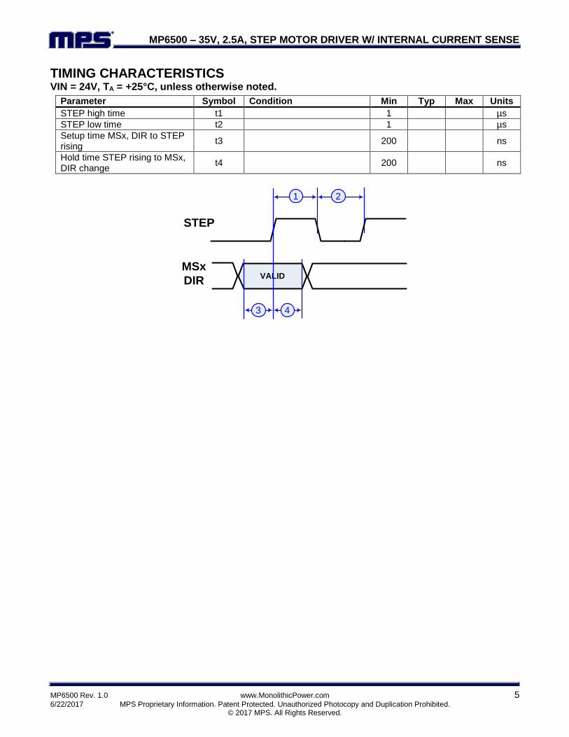
TIMING CHARACTERISTICS VIN = 24V, TA = +25°C, unless otherwise noted.
Parameter Symbol Condition Min Typ Max Units
STEP high time t1 1 µs
STEP low time t2 1 µs
Setup time MSx, DIR to STEP rising
t3
200 ns
Hold time STEP rising to MSx, DIR change
t4
200 ns
VALID
STEP
MSx
DIR
21
43
MP6500 – 35V, 2.5A, STEP MOTOR DRIVER W/ INTERNAL CURRENT SENSE
MP6500 Rev. 1.0 www.MonolithicPower.com 6
6/22/2017 MPS Proprietary Information. Patent Protected. Unauthorized Photocopy and Duplication Prohibited. © 2017 MPS. All Rights Reserved.
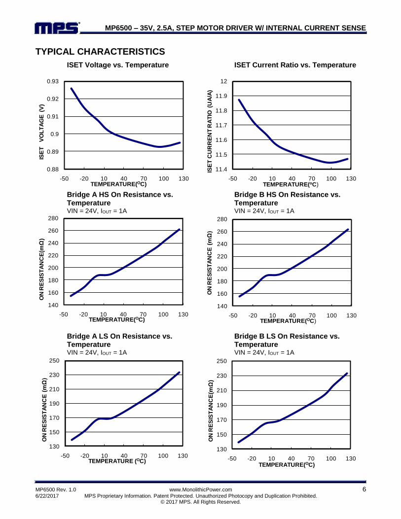
TYPICAL CHARACTERISTICS
ISET Voltage vs. Temperature
ISET Current Ratio vs. Temperature
Bridge A HS On Resistance vs.
Temperature VIN = 24V, IOUT = 1A
Bridge B HS On Resistance vs. Temperature VIN = 24V, IOUT = 1A
Bridge A LS On Resistance vs. Temperature VIN = 24V, IOUT = 1A
Bridge B LS On Resistance vs. Temperature VIN = 24V, IOUT = 1A
0.88
0.89
0.9
0.91
0.92
0.93
-50 -20 10 40 70 100 130
ISE
T V
OL
TA
GE
(V
)
TEMPERATURE(OC)
11.4
11.5
11.6
11.7
11.8
11.9
12
-50 -20 10 40 70 100 130
ISE
T C
UR
RE
NT
RA
TIO
(U
A/A
)
TEMPERATURE(oC)
140
160
180
200
220
240
260
280
-50 -20 10 40 70 100 130
ON
RE
SIS
TA
NC
E(m
Ω)
TEMPERATURE(OC)
140
160
180
200
220
240
260
280
-50 -20 10 40 70 100 130
ON
RE
SIS
TA
NC
E (
mΩ
)
TEMPERATURE(OC)
130
150
170
190
210
230
250
-50 -20 10 40 70 100 130
ON
RE
SIS
TA
NC
E (
mΩ
)
TEMPERATURE (OC)
130
150
170
190
210
230
250
-50 -20 10 40 70 100 130
ON
RE
SIS
TA
NC
E(m
Ω)
TEMPERATURE(OC)
MP6500 – 35V, 2.5A, STEP MOTOR DRIVER W/ INTERNAL CURRENT SENSE
MP6500 Rev. 1.0 www.MonolithicPower.com 7
6/22/2017 MPS Proprietary Information. Patent Protected. Unauthorized Photocopy and Duplication Prohibited. © 2017 MPS. All Rights Reserved.
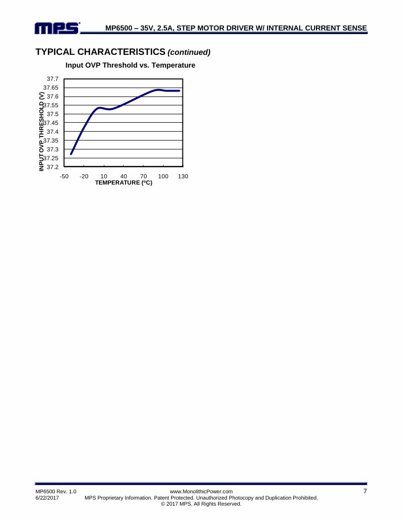
TYPICAL CHARACTERISTICS (continued)
Input OVP Threshold vs. Temperature
37.2
37.25
37.3
37.35
37.4
37.45
37.5
37.55
37.6
37.65
37.7
-50 -20 10 40 70 100 130
INP
UT
OV
P T
HR
ES
HO
LD
(V
)
TEMPERATURE (oC)
MP6500 – 35V, 2.5A, STEP MOTOR DRIVER W/ INTERNAL CURRENT SENSE
MP6500 Rev. 1.0 www.MonolithicPower.com 8
6/22/2017 MPS Proprietary Information. Patent Protected. Unauthorized Photocopy and Duplication Prohibited. © 2017 MPS. All Rights Reserved.
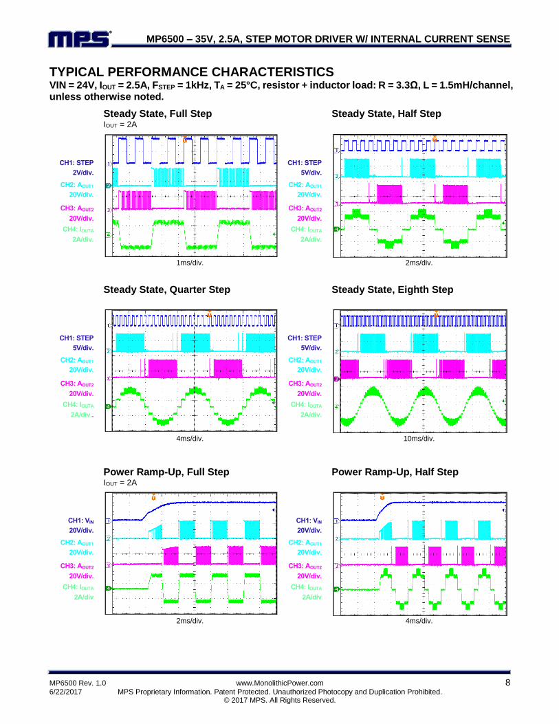
TYPICAL PERFORMANCE CHARACTERISTICS VIN = 24V, IOUT = 2.5A, FSTEP = 1kHz, TA = 25°C, resistor + inductor load: R = 3.3Ω, L = 1.5mH/channel, unless otherwise noted.
Steady State, Full Step IOUT = 2A
Steady State, Half Step
CH1: STEP
2V/div.
CH2: AOUT1
20V/div.
CH3: AOUT2
20V/div.
CH4: IOUTA
2A/div.
CH1: STEP
5V/div.
CH2: AOUT1
20V/div.
CH3: AOUT2
20V/div.
CH4: IOUTA
2A/div.
1ms/div. 2ms/div.
Steady State, Quarter Step
Steady State, Eighth Step
CH1: STEP
5V/div.
CH2: AOUT1
20V/div.
CH3: AOUT2
20V/div.
CH4: IOUTA
2A/div..
CH1: STEP
5V/div.
CH2: AOUT1
20V/div.
CH3: AOUT2
20V/div.
CH4: IOUTA
2A/div.
4ms/div. 10ms/div.
Power Ramp-Up, Full Step IOUT = 2A
Power Ramp-Up, Half Step
CH1: VIN
20V/div.
CH2: AOUT1
20V/div.
CH3: AOUT2
20V/div.
CH4: IOUTA
2A/div
CH1: VIN
20V/div.
CH2: AOUT1
20V/div.
CH3: AOUT2
20V/div.
CH4: IOUTA
2A/div
2ms/div. 4ms/div.
MP6500 – 35V, 2.5A, STEP MOTOR DRIVER W/ INTERNAL CURRENT SENSE
MP6500 Rev. 1.0 www.MonolithicPower.com 9
6/22/2017 MPS Proprietary Information. Patent Protected. Unauthorized Photocopy and Duplication Prohibited. © 2017 MPS. All Rights Reserved.
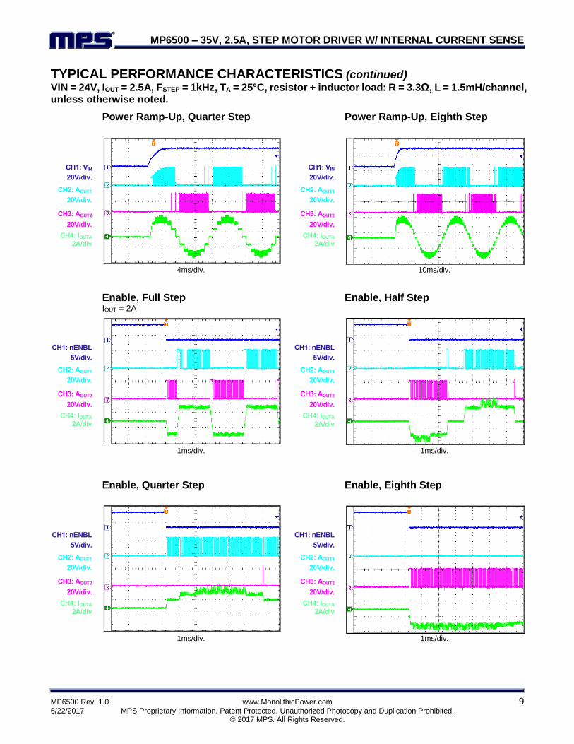
TYPICAL PERFORMANCE CHARACTERISTICS (continued) VIN = 24V, IOUT = 2.5A, FSTEP = 1kHz, TA = 25°C, resistor + inductor load: R = 3.3Ω, L = 1.5mH/channel, unless otherwise noted.
Power Ramp-Up, Quarter Step
Power Ramp-Up, Eighth Step
CH1: VIN
20V/div.
CH2: AOUT1
20V/div.
CH3: AOUT2
20V/div.
CH4: IOUTA 2A/div
CH1: VIN
20V/div.
CH2: AOUT1
20V/div.
CH3: AOUT2
20V/div.
CH4: IOUTA 2A/div
4ms/div. 10ms/div.
Enable, Full Step IOUT = 2A
Enable, Half Step
CH1: nENBL
5V/div.
CH2: AOUT1
20V/div.
CH3: AOUT2
20V/div.
CH4: IOUTA 2A/div
CH1: nENBL
5V/div.
CH2: AOUT1
20V/div.
CH3: AOUT2
20V/div.
CH4: IOUTA
2A/div
1ms/div. 1ms/div.
Enable, Quarter Step
Enable, Eighth Step
CH1: nENBL
5V/div.
CH2: AOUT1
20V/div.
CH3: AOUT2
20V/div.
CH4: IOUTA
2A/div
CH1: nENBL
5V/div.
CH2: AOUT1
20V/div.
CH3: AOUT2
20V/div.
CH4: IOUTA
2A/div
1ms/div. 1ms/div.
MP6500 – 35V, 2.5A, STEP MOTOR DRIVER W/ INTERNAL CURRENT SENSE
MP6500 Rev. 1.0 www.MonolithicPower.com 10
6/22/2017 MPS Proprietary Information. Patent Protected. Unauthorized Photocopy and Duplication Prohibited. © 2017 MPS. All Rights Reserved.
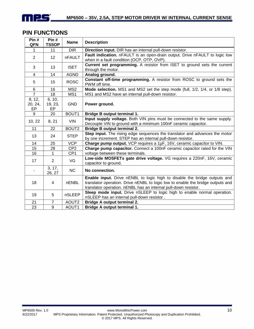
PIN FUNCTIONS Pin # QFN
Pin # TSSOP
Name Description
1 11 DIR Direction input. DIR has an internal pull-down resistor.
2 12 nFAULT Fault indication. nFAULT is an open-drain output. Drive nFAULT to logic low when in a fault condition (OCP, OTP, OVP).
3 13 ISET Current set programming. A resistor from ISET to ground sets the current through the motor.
4 14 AGND Analog ground.
5 15 ROSC Constant off-time programming. A resistor from ROSC to ground sets the PWM off time.
6 16 MS2 Mode selection. MS1 and MS2 set the step mode (full, 1/2, 1/4, or 1/8 step). MS1 and MS2 have an internal pull-down resistor. 7 18 MS1
8, 12, 20, 24,
EP
6, 10, 19, 23,
EP GND Power ground.
9 20 BOUT1 Bridge B output terminal 1.
10, 22 8, 21 VIN Input supply voltage. Both VIN pins must be connected to the same supply. Decouple VIN to ground with a minimum 100nF ceramic capacitor.
11 22 BOUT2 Bridge B output terminal 2.
13 24 STEP Step input. The rising edge sequences the translator and advances the motor by one increment. STEP has an internal pull-down resistor.
14 25 VCP Charge pump output. VCP requires a 1µF, 16V, ceramic capacitor to VIN.
15 28 CP2 Charge pump capacitor. Connect a 100nF ceramic capacitor rated for the VIN voltage between these terminals. 16 1 CP1
17 2 VG Low-side MOSFETs gate drive voltage. VG requires a 220nF, 16V, ceramic capacitor to ground.
- 3, 17, 26, 27
NC No connection.
18 4 nENBL Enable input. Drive nENBL to logic high to disable the bridge outputs and translator operation. Drive nENBL to logic low to enable the bridge outputs and translator operation. nENBL has an internal pull-down resistor.
19 5 nSLEEP Sleep mode input. Drive nSLEEP to logic high to enable normal operation. nSLEEP has an internal pull-down resistor .
21 7 AOUT2 Bridge A output terminal 2.
23 9 AOUT1 Bridge A output terminal 1.

MP6500 – 35V, 2.5A, STEP MOTOR DRIVER W/ INTERNAL CURRENT SENSE
MP6500 Rev. 1.0 www.MonolithicPower.com 11
6/22/2017 MPS Proprietary Information. Patent Protected. Unauthorized Photocopy and Duplication Prohibited. © 2017 MPS. All Rights Reserved.
BLOCK DIAGRAM
Gate
Driver
Gate
Driver
Control
Logic
VREF
Int. VCC
LS Gate
Drive V
Motor
Charge
PumpCPA
CPB
VCP
AOUT1
AOUT2
BOUT1
BOUT2
ROSC
DIR
nENBL
MS1
MS2
nSLEEP
µC
VINMP6500
nFAULT
ISENSE
PWM
Timer
UVLO
OVP
OTS
VG
STEPCurr.
Reg.
ISENSE
Curr.
Reg.
ISET
VIN
VIN
VIN
GND
Figure 1: Functional Block Diagram
MP6500 – 35V, 2.5A, STEP MOTOR DRIVER W/ INTERNAL CURRENT SENSE
MP6500 Rev. 1.0 www.MonolithicPower.com 12
6/22/2017 MPS Proprietary Information. Patent Protected. Unauthorized Photocopy and Duplication Prohibited. © 2017 MPS. All Rights Reserved.
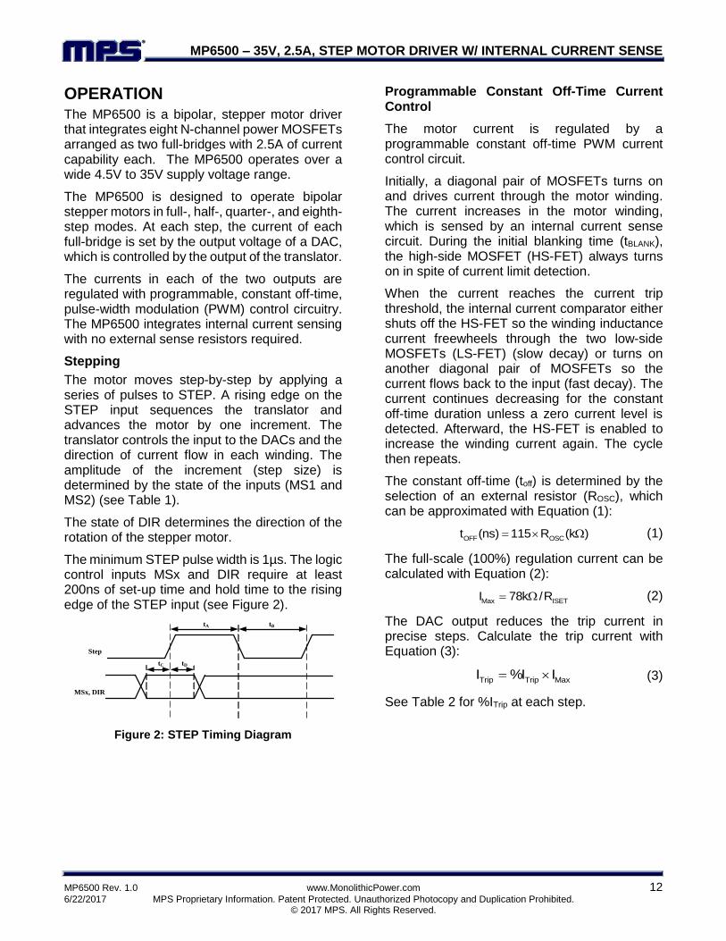
OPERATION The MP6500 is a bipolar, stepper motor driver that integrates eight N-channel power MOSFETs arranged as two full-bridges with 2.5A of current capability each. The MP6500 operates over a wide 4.5V to 35V supply voltage range.
The MP6500 is designed to operate bipolar stepper motors in full-, half-, quarter-, and eighth-step modes. At each step, the current of each full-bridge is set by the output voltage of a DAC, which is controlled by the output of the translator.
The currents in each of the two outputs are regulated with programmable, constant off-time, pulse-width modulation (PWM) control circuitry. The MP6500 integrates internal current sensing with no external sense resistors required.
Stepping
The motor moves step-by-step by applying a series of pulses to STEP. A rising edge on the STEP input sequences the translator and advances the motor by one increment. The translator controls the input to the DACs and the direction of current flow in each winding. The amplitude of the increment (step size) is determined by the state of the inputs (MS1 and MS2) (see Table 1).
The state of DIR determines the direction of the rotation of the stepper motor.
The minimum STEP pulse width is 1µs. The logic control inputs MSx and DIR require at least 200ns of set-up time and hold time to the rising edge of the STEP input (see Figure 2).
Step
MSx, DIR
tA tB
tC tD
Figure 2: STEP Timing Diagram
Programmable Constant Off-Time Current Control
The motor current is regulated by a programmable constant off-time PWM current control circuit.
Initially, a diagonal pair of MOSFETs turns on and drives current through the motor winding. The current increases in the motor winding, which is sensed by an internal current sense circuit. During the initial blanking time (tBLANK), the high-side MOSFET (HS-FET) always turns on in spite of current limit detection.
When the current reaches the current trip threshold, the internal current comparator either shuts off the HS-FET so the winding inductance current freewheels through the two low-side MOSFETs (LS-FET) (slow decay) or turns on another diagonal pair of MOSFETs so the current flows back to the input (fast decay). The current continues decreasing for the constant off-time duration unless a zero current level is detected. Afterward, the HS-FET is enabled to increase the winding current again. The cycle then repeats.
The constant off-time (toff) is determined by the selection of an external resistor (ROSC), which can be approximated with Equation (1):
OFF OSCt (ns) 115 R (k ) (1)
The full-scale (100%) regulation current can be calculated with Equation (2):
Max ISETI 78k /R (2)
The DAC output reduces the trip current in precise steps. Calculate the trip current with Equation (3):
Trip Trip MaxI %I I (3)
See Table 2 for %ITrip at each step.
MP6500 – 35V, 2.5A STEP MOTOR DRIVER W/ INTERNAL CURRENT SENSE
MP6500 Rev. 1.0 www.MonolithicPower.com 13
6/22/2017 MPS Proprietary Information. Patent Protected. Unauthorized Photocopy and Duplication Prohibited. © 2017 MPS. All Rights Reserved.
Blanking Time
There is usually a current spike during the switching transition due to the body diode’s reverse-recovery current and the distributed winding capacitance of the motor. This current spike requires filtering to prevent it from erroneously shutting down the HS-FET.
After the PWM cycle begins, the output of the current sense comparator is ignored for the fixed blanking time. This blanking time results in a minimum on time for the PWM cycle.
Automatic Decay Mode
The MP6500 uses a fully automatic decay mode to provide accurate current regulation.
Initially, slow decay is used. At the end of the fixed off time, if the current is above the ITRIP
threshold, then fast decay mode is initiated by reversing the state of the H-bridge outputs.
Once the current level during this fast decay period drops below the ITRIP threshold, slow decay is again engaged for another fixed off time. After the completion of this second fixed off time, a new PWM cycle begins.
Figure 3 below shows the automatic decay mode operation during a current reduction as a result of a step input.
tOFF
IOUT
ITRIP
Slow Decay During tOFF Unless
IOUT > ITRIP at end of tOFF
tOFF tOFF tOFF tOFF2 tOFF tOFF tOFF
Fast
Decay
ITRIP
Change
Slow
Decay
Figure 3: Slow Decay During tOFF unless IOUT > ITRIP at end of tOFF
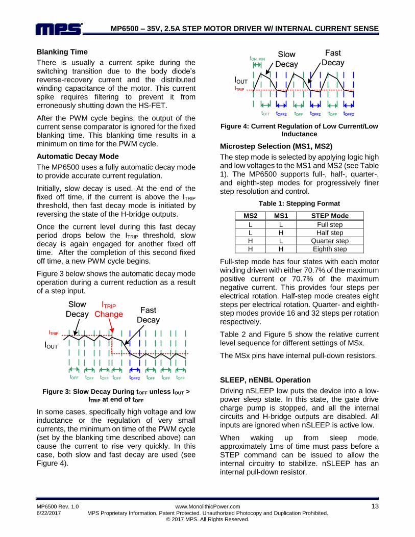
In some cases, specifically high voltage and low inductance or the regulation of very small currents, the minimum on time of the PWM cycle (set by the blanking time described above) can cause the current to rise very quickly. In this case, both slow and fast decay are used (see Figure 4).
tOFF
IOUT
ITRIP
Current regulation of low
current / low inductance
tOFF
Fast
Decay
tOFF2 tOFFtOFF2 tOFF2
Slow
DecaytON_MIN
Figure 4: Current Regulation of Low Current/Low Inductance
Microstep Selection (MS1, MS2)
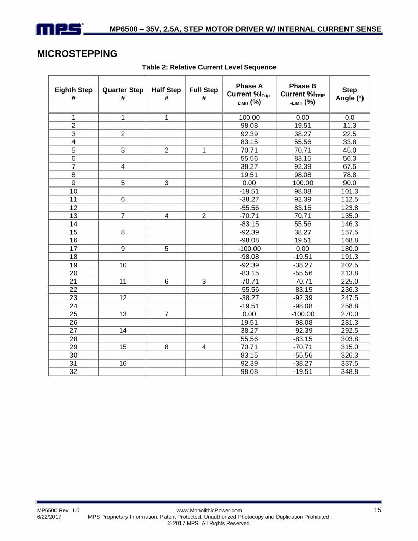
The step mode is selected by applying logic high and low voltages to the MS1 and MS2 (see Table 1). The MP6500 supports full-, half-, quarter-, and eighth-step modes for progressively finer step resolution and control.
Table 1: Stepping Format
MS2 MS1 STEP Mode
L L Full step
L H Half step
H L Quarter step
H H Eighth step
Full-step mode has four states with each motor winding driven with either 70.7% of the maximum positive current or 70.7% of the maximum negative current. This provides four steps per electrical rotation. Half-step mode creates eight steps per electrical rotation. Quarter- and eighth-step modes provide 16 and 32 steps per rotation respectively.
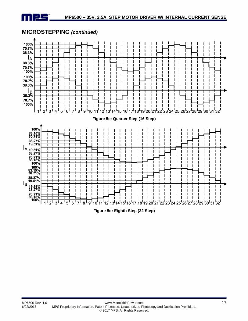
Table 2 and Figure 5 show the relative current level sequence for different settings of MSx.
The MSx pins have internal pull-down resistors.
SLEEP, nENBL Operation
Driving nSLEEP low puts the device into a low-power sleep state. In this state, the gate drive charge pump is stopped, and all the internal circuits and H-bridge outputs are disabled. All inputs are ignored when nSLEEP is active low.
When waking up from sleep mode, approximately 1ms of time must pass before a STEP command can be issued to allow the internal circuitry to stabilize. nSLEEP has an internal pull-down resistor.
MP6500 – 35V, 2.5A STEP MOTOR DRIVER W/ INTERNAL CURRENT SENSE
MP6500 Rev. 1.0 www.MonolithicPower.com 14
6/22/2017 MPS Proprietary Information. Patent Protected. Unauthorized Photocopy and Duplication Prohibited. © 2017 MPS. All Rights Reserved.
The nENBL pin is used to control the output drivers. When nENBL is low, the output H-bridge outputs are enabled, and the rising edges on STEP are recognized. When nENBL is high, the H-bridge outputs are disabled, and the STEP input is ignored. nENBL has an internal pull-down resistor.
Fault Reporting
The MP6500 provides an nFAULT pin, which reports if a fault condition (such as OCP, OTP, or OVP) occurs. nFAULT is an open-drain output and is driven low when a fault condition occurs. If the fault condition is removed, nFAULT is pulled high by an external pull-up resistor.
Over-Current Protection (OCP)
Over-current protection (OCP) circuitry limits the current through the MOSFETs by disabling the gate driver. If the over-current limit threshold is exceeded for longer than the over-current deglitch time, all MOSFETs in the H-bridge are disabled, and nFAULT is driven low. The driver remains disabled for 2.4ms typically, at which time it is re-enabled automatically.
Over-current conditions on both high- and low-side devices (i.e.: a short to ground, supply, or across the motor winding) result in an over-current shutdown. Note that OCP does not use the current sense circuitry used for PWM current control.
Over-Voltage Protection (OVP)
If the input voltage on VIN is higher than the over-voltage protection (OVP) threshold, the H-bridge output is disabled, and nFAULT is driven low. This protection is released when VIN drops below 36V.
Input Under-Voltage Lockout (UVLO) Protection
If at any time the voltage on VIN falls below the under-voltage lockout (UVLO) threshold voltage, all circuitry in the device is disabled, and the internal logic is reset. Operation resumes when VIN rises above the UVLO threshold.
Thermal Shutdown
If the die temperature exceeds safe limits, all MOSFETs in the H-bridge are disabled, and nFAULT is driven low. Once the die temperature has fallen to a safe level, operation resumes automatically.
MP6500 – 35V, 2.5A, STEP MOTOR DRIVER W/ INTERNAL CURRENT SENSE
MP6500 Rev. 1.0 www.MonolithicPower.com 15
6/22/2017 MPS Proprietary Information. Patent Protected. Unauthorized Photocopy and Duplication Prohibited. © 2017 MPS. All Rights Reserved.
MICROSTEPPING
Table 2: Relative Current Level Sequence
Eighth Step #
Quarter Step #
Half Step #
Full Step #
Phase A Current %ITrip-
LIMIT (%)
Phase B Current %ITRIP
-LIMIT (%)
Step Angle (°)
1 1 1 100.00 0.00 0.0
2 98.08 19.51 11.3
3 2 92.39 38.27 22.5
4 83.15 55.56 33.8
5 3 2 1 70.71 70.71 45.0
6 55.56 83.15 56.3
7 4 38.27 92.39 67.5
8 19.51 98.08 78.8
9 5 3 0.00 100.00 90.0
10 -19.51 98.08 101.3
11 6 -38.27 92.39 112.5
12 -55.56 83.15 123.8
13 7 4 2 -70.71 70.71 135.0
14 -83.15 55.56 146.3
15 8 -92.39 38.27 157.5
16 -98.08 19.51 168.8
17 9 5 -100.00 0.00 180.0
18 -98.08 -19.51 191.3
19 10 -92.39 -38.27 202.5
20 -83.15 -55.56 213.8
21 11 6 3 -70.71 -70.71 225.0
22 -55.56 -83.15 236.3
23 12 -38.27 -92.39 247.5
24 -19.51 -98.08 258.8
25 13 7 0.00 -100.00 270.0
26 19.51 -98.08 281.3
27 14 38.27 -92.39 292.5
28 55.56 -83.15 303.8
29 15 8 4 70.71 -70.71 315.0
30 83.15 -55.56 326.3
31 16 92.39 -38.27 337.5
32 98.08 -19.51 348.8

MP6500 – 35V, 2.5A, STEP MOTOR DRIVER W/ INTERNAL CURRENT SENSE
MP6500 Rev. 1.0 www.MonolithicPower.com 16
6/22/2017 MPS Proprietary Information. Patent Protected. Unauthorized Photocopy and Duplication Prohibited. © 2017 MPS. All Rights Reserved.
MICROSTEPPING (continued)
Figure 5a: Full Step (4 Step Sequences)
Figure 5b: Half Step (8 Step Sequences)
MP6500 – 35V, 2.5A, STEP MOTOR DRIVER W/ INTERNAL CURRENT SENSE
MP6500 Rev. 1.0 www.MonolithicPower.com 17
6/22/2017 MPS Proprietary Information. Patent Protected. Unauthorized Photocopy and Duplication Prohibited. © 2017 MPS. All Rights Reserved.
MICROSTEPPING (continued)
Figure 5c: Quarter Step (16 Step)
Figure 5d: Eighth Step (32 Step)

MP6500 – 35V, 2.5A, STEP MOTOR DRIVER W/ INTERNAL CURRENT SENSE
MP6500 Rev. 1.0 www.MonolithicPower.com 18
6/22/2017 MPS Proprietary Information. Patent Protected. Unauthorized Photocopy and Duplication Prohibited. © 2017 MPS. All Rights Reserved.
PACKAGE INFORMATION
QFN-24 (5mmx5mm)
SIDE VIEW
BOTTOM VIEW
NOTE:
1) ALL DIMENSIONS ARE IN MILLIMETERS.
2) EXPOSED PADDLE SIZE DOES NOT
INCLUDE MOLD FLASH.
3) LEAD COPLANARITY SHALL BE 0.10
MILLIMETERS MAX.
4) DRAWING CONFIRMS TO JEDEC MO-220.
5) DRAWING IS NOT TO SCALE.
PIN 1 ID
MARKING
TOP VIEW
PIN 1 ID INDEX
AREA
RECOMMENDED LAND PATTERN
PIN 1 ID
0.30x45° TYP.
MP6500 – 35V, 2.5A, STEP MOTOR DRIVER W/ INTERNAL CURRENT SENSE
NOTICE: The information in this document is subject to change without notice. Please contact MPS for current specifications.
Users should warrant and guarantee that third party Intellectual Property rights are not infringed upon when integrating MPS products into any application. MPS will not assume any legal responsibility for any said applications.
MP6500 Rev. 1.0 www.MonolithicPower.com 19
6/22/2017 MPS Proprietary Information. Patent Protected. Unauthorized Photocopy and Duplication Prohibited. © 2017 MPS. All Rights Reserved.
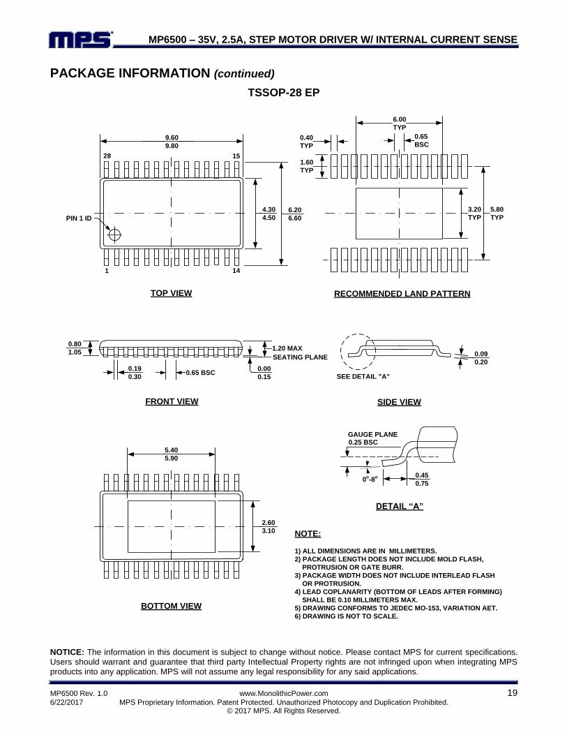
PACKAGE INFORMATION (continued)
TSSOP-28 EP PACKAGE OUTLINE DRAWING FOR 28-TSSOP w/ EXPOSED PADDLE
MF-PO-D-0055 revision 2.0
SIDE VIEW
NOTE:
1) ALL DIMENSIONS ARE IN MILLIMETERS.
2) PACKAGE LENGTH DOES NOT INCLUDE MOLD FLASH,
PROTRUSION OR GATE BURR.
3) PACKAGE WIDTH DOES NOT INCLUDE INTERLEAD FLASH
OR PROTRUSION.
4) LEAD COPLANARITY (BOTTOM OF LEADS AFTER FORMING)
SHALL BE 0.10 MILLIMETERS MAX.
5) DRAWING CONFORMS TO JEDEC MO-153, VARIATION AET.
6) DRAWING IS NOT TO SCALE.
DETAIL “A”
0.45
0.750
o-8
o
0.25 BSCGAUGE PLANE
9.60
9.80
PIN 1 ID
4.30
4.506.20
6.60
1 14
1528
TOP VIEW
0.09
0.20
SEE DETAIL "A"
BOTTOM VIEW
2.60
3.10
5.40
5.90
0.19
0.30
SEATING PLANE
0.65 BSC
0.80
1.051.20 MAX
0.00
0.15
FRONT VIEW
RECOMMENDED LAND PATTERN
5.80
TYP
1.60
TYP
0.40
TYP
0.65
BSC
3.20
TYP
6.00
TYP
Related Documents