MOSTEC Devices Fabrication Gain the experience of IC fabrication! Authors: Ibrahim Muhammad Elsaeed Aya Saleh Mahmoud Hossam El-Anzery Wael Abdullah Yousry Elmaghraby Dr. Bassem Abdullah Prof. Ashraf Salem www.tiec.gov

Welcome message from author
This document is posted to help you gain knowledge. Please leave a comment to let me know what you think about it! Share it to your friends and learn new things together.
Transcript
MOSTEC Devices Fabrication Gain the experience of IC fabrication!
Authors:
Ibrahim Muhammad Elsaeed
Aya Saleh Mahmoud
Hossam El-Anzery
Wael Abdullah
Yousry Elmaghraby
Dr. Bassem Abdullah
Prof. Ashraf Salem
www.tiec.gov.eg
MOSTEC Devices Fabrication
2 Technology Innovation and Entrepreneurship Center (TIEC)
Abstract TIEC in collaboration with CIME decided to organize an intensive 5-days training program dedicated to
IC fabrication. The objective of this training program is to give the basic knowledge for silicon
technology applications. This course included hands-on training and experiments in clean room. The
program started by a presentation on Grenoble, CIME Nanotech and its technological environment.
The program was divided into three modules. Module 1 is a 3-days on the basic integration process for
MOSFET and clean rooms technology process for CMOS fabrication. Module 2 is a one-day training
focusing on Electrical characterization of CMOS devices. Module 3 is also a one-day training Modeling
and Technology Computer Aided Design.
MOSTEC Devices Fabrication
3 Technology Innovation and Entrepreneurship Center (TIEC)
Contents Introduction
Photolithography of field oxide
Polysilicon gate – Photolithograhy
Polysilicon gate – Dry Etching (RIE)
Polysilicon gate – Photoresist Etching
Doping by Ion-Implantation
Wafer cleaning before thermal annealing
Thermal Annealing
Protective Oxide Deposition
Protective Oxide Photolithography
Aluminum Contact – Sputtering
Aluminum Contact – Photolithography
Removing the backside Polysilicon
Electrical Testing
Silvaco TCAD tools
Course Organization
Conclusion

MOSTEC Devices Fabrication
4 Technology Innovation and Entrepreneurship Center (TIEC)
Introduction
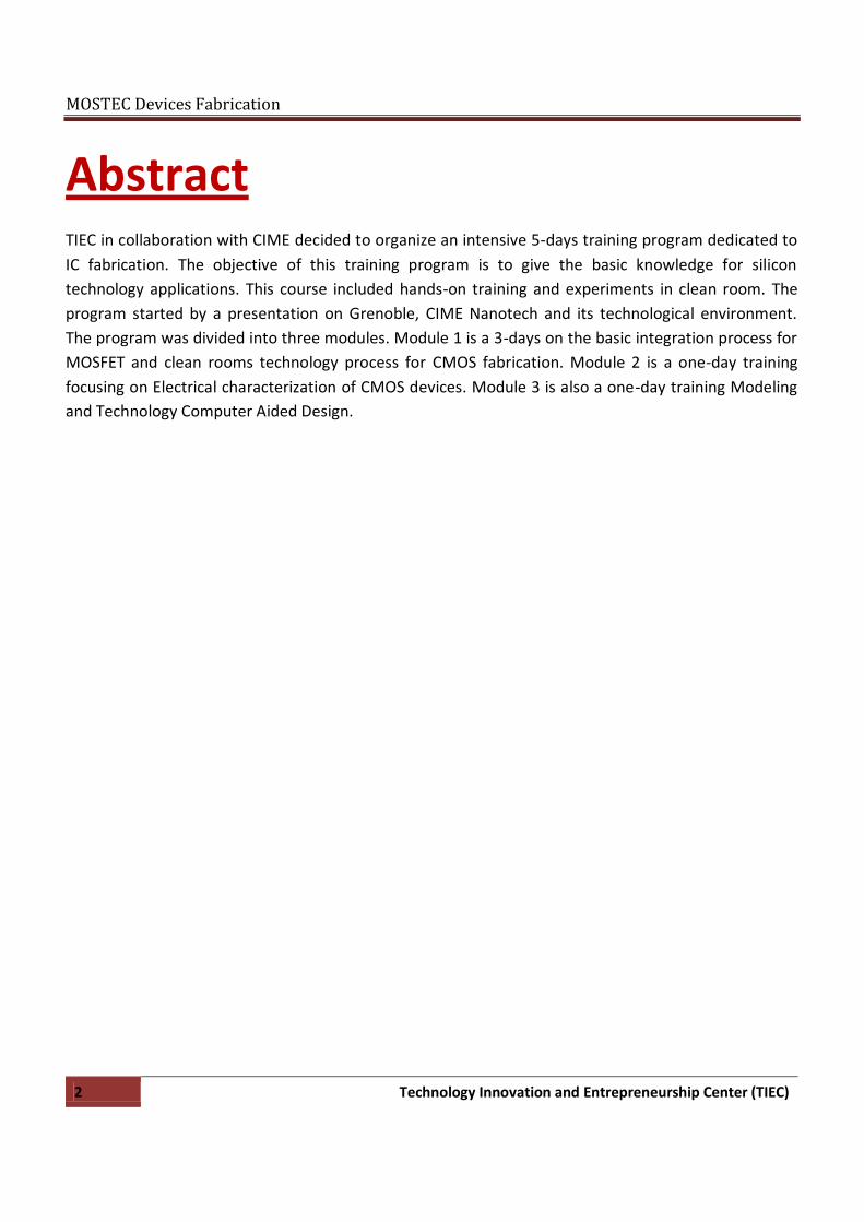
IC Fabrication is now one of the essential processes of the human life. Mobile phones, desktop
computers, laptops and many other essential electronic devices that one can't get rid of them are all
related to the IC Fabrication. As an attempt for spreading the knowledge of how ICs are being
fabricated, this white paper aims to transfer a true experience of how ICs are fabricated. Steps,
Machines and every little detail will be discussed in this paper.
Grenoble is a city in south-eastern France, at the foot of the French Alps where the river Drac joins
the Isère. Located in the Rhône-Alpes region, Grenoble is being known in France as the "Capital of the
Alps". Grenoble is also a major scientific centre, especially in the fields of physics, computer science,
and applied mathematics: Joseph Fourier University (UJF) is one of the leading French scientific
universities while the Grenoble Institute of Technology trains more than 5,000 engineers every year in
key technology disciplines. Grenoble's high tech expertise is organized mainly around three domains:
information technology, biotechnologies and new technologies of energy and nanotechnology.
Many fundamental and applied scientific research laboratories are conjointly managed by Joseph Fourier University, Grenoble Institute of Technology, and the French National Centre for Scientific Research (CNRS). Numerous other scientific laboratories are managed independently or in collaboration with the CNRS and the French National Institute for Research in Computer Science and Control (INRIA).
CIME Nanotech is the most important center in the French National Network for Education in
Microelectronics and Nanotechnology. The CIME Nanotech is an academic center for education and
research in microelectronics and nanotechnology. Founded in 1981, it is operated jointly by the Joseph
Fourier University, the science Grenoble University and by the Grenoble Institute of Technology
(Grenoble INP). 12 universities are using the CIME Nanotech facilities each year. CIME hosts 1500
students annually with 140 instructors supervising the education programs. There are 8 technology
platforms using the cleanroom facilities in this huge center. Those platforms are: IC Design,
Biotechnology, Nano-characterization, embedded systems, RF systems, Electrical test and sensors &
MEMS.
CIME Nanotech provides its users with a complete process integration line on 100mm silicon wafer
diameter. Training programs in MOS technology and in MEMS fields are available for different
universities and used by electronic engineers’ courses. The main idea is to bring the engineers in
contact with the main technology process that is used in building Microelectronic devices.
MOSTEC Devices Fabrication
5 Technology Innovation and Entrepreneurship Center (TIEC)
This paper is organized with the same order of the steps that would be followed for fabricating and
testing a chip. First, the photolithography process is described; this process actually is needed in many
other processes whenever a layout is to be transferred on the wafer. Second, the polysilicon gate
process is described, showing the different steps followed in making the gate of the transistors. Third,
the ion-implantation is described with the thermal annealing. Fourth, the aluminum contacts, which
are used as pins in testing, process is described. Fifth, chip testing is described, showing how the chips
after fabrication are tested in lab. Finally, a simulation for the whole processes is described using
SILVACO.
MOSTEC Devices Fabrication
6 Technology Innovation and Entrepreneurship Center (TIEC)
Photolithography of Field Oxide
As a beginning, we got the wafer with thermal oxide growth, as this step takes time. We are going to
begin our steps after the Oxidation step. The wafer looks as figure (1)
We need to draw the active parts that will be doped later and contain Poly-silicon gate. The steps;
1) Photolithography
2) Wet etching
3) Removal of photo-resist.
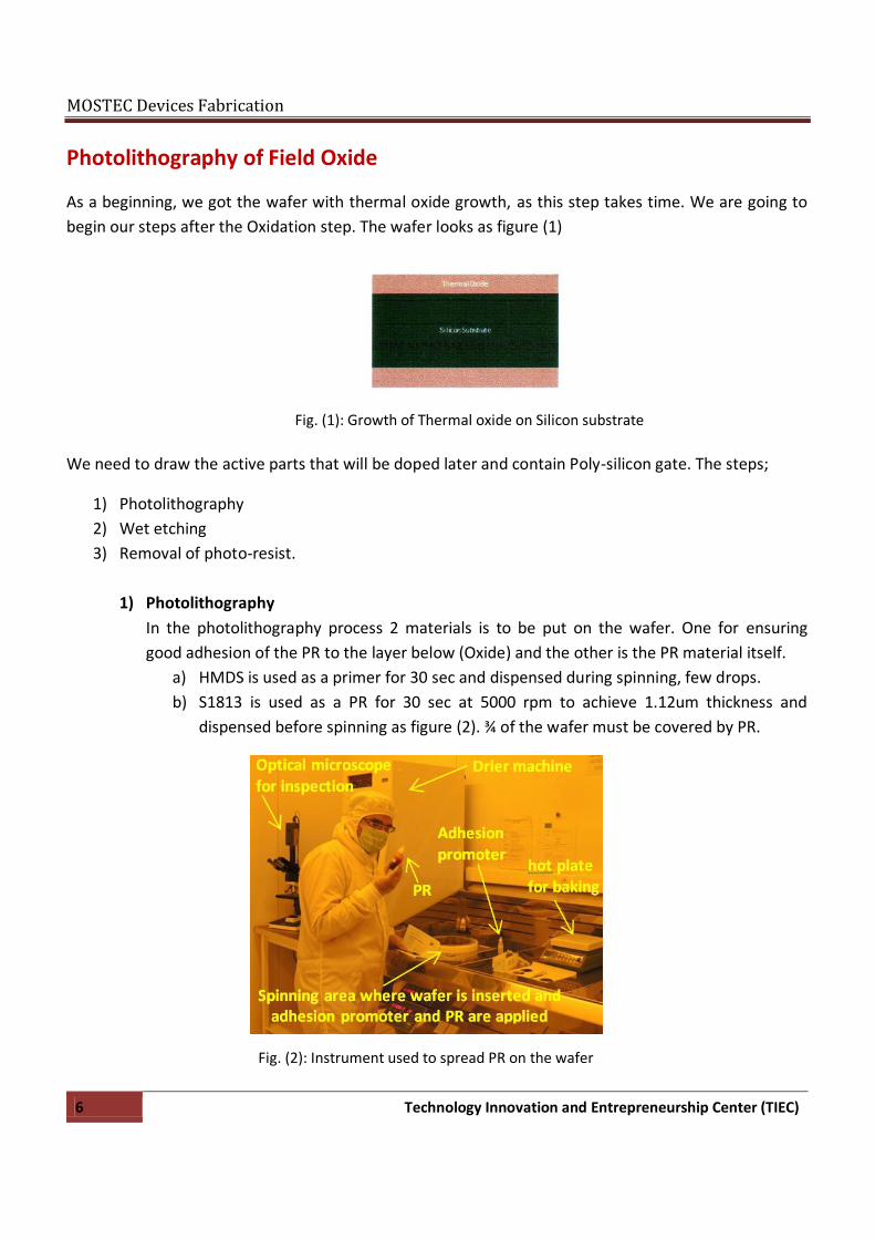
1) Photolithography
In the photolithography process 2 materials is to be put on the wafer. One for ensuring
good adhesion of the PR to the layer below (Oxide) and the other is the PR material itself.
a) HMDS is used as a primer for 30 sec and dispensed during spinning, few drops.
b) S1813 is used as a PR for 30 sec at 5000 rpm to achieve 1.12um thickness and
dispensed before spinning as figure (2). ¾ of the wafer must be covered by PR.
Fig. (2): Instrument used to spread PR on the wafer
Fig. (1): Growth of Thermal oxide on Silicon substrate

MOSTEC Devices Fabrication
7 Technology Innovation and Entrepreneurship Center (TIEC)
c) Soft baking at 120 °C for 2:30 min see figure(3). If we exposed for longer time, the PR
will be less sensitive to UV.
d) Using Contact printing for 30 sec with mercury source, no need for alignment as it
was the first mask. See figure(4)
e) Development step: rinse the container with DI-water, then develop the wafer for 2
min, then remove the developer by DI-water & then keep it in running DI-water see
figure(5) and measure its resistivity till it reaches 18MΩ-cm (resistivity of DI-water).
Fig. (3): heater used in soft and hard
baking
Fig. (4): instrument where the mask exposed to UV
Hot Plate for
baking
Wafers
MOSTEC Devices Fabrication
8 Technology Innovation and Entrepreneurship Center (TIEC)
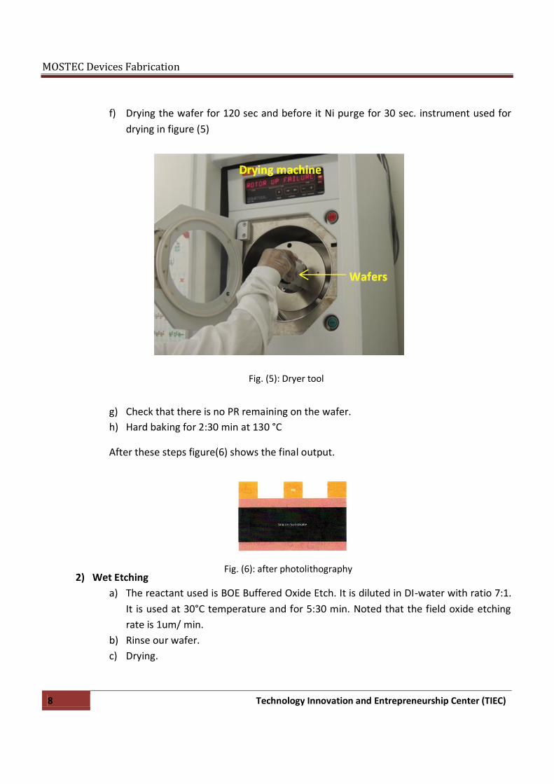
f) Drying the wafer for 120 sec and before it Ni purge for 30 sec. instrument used for
drying in figure (5)
g) Check that there is no PR remaining on the wafer.
h) Hard baking for 2:30 min at 130 °C
After these steps figure(6) shows the final output.
2) Wet Etching
a) The reactant used is BOE Buffered Oxide Etch. It is diluted in DI-water with ratio 7:1.
It is used at 30°C temperature and for 5:30 min. Noted that the field oxide etching
rate is 1um/ min.
b) Rinse our wafer.
c) Drying.
Fig. (5): Dryer tool
Fig. (6): after photolithography
MOSTEC Devices Fabrication
9 Technology Innovation and Entrepreneurship Center (TIEC)
The final result is shown in figure (7)
3) Removal of PR
a) Special transparent reactant is used to get rid of PR. When this transparent reactant
turns red when PR is removed. It used at 20 °C for 2 min.
b) Rinsing the material in DI water to get rid of any remaining PR, keep in rinse till the
Di-water resistivity reaches 18MΩ-cm.
c) Drying for 120 sec.
The final output is shown in figure(8)
In the next phases consider that the polysilicon is deposited on the wafer.
Poly-silicon gate photolithography
Now, as we have the poly-silicon layer deposited ready for the gate to be drawn on it using
photolithography. Another layer of photoresist is to be put over the poly-silicon layer.
The rest of the photolithography process flow is to be done over the wafer for completing the transfer
of the Gate poly. Finally we would get the following wafer cross-section figure(9).
The next step is to etch (remove) the undesired poly-silicon from the whole wafer surface except that
under the PR which will be our Gate poly-silicon.
Fig. (7): after wet etching
Fig. (8): results from removal of PR

MOSTEC Devices Fabrication
10 Technology Innovation and Entrepreneurship Center (TIEC)
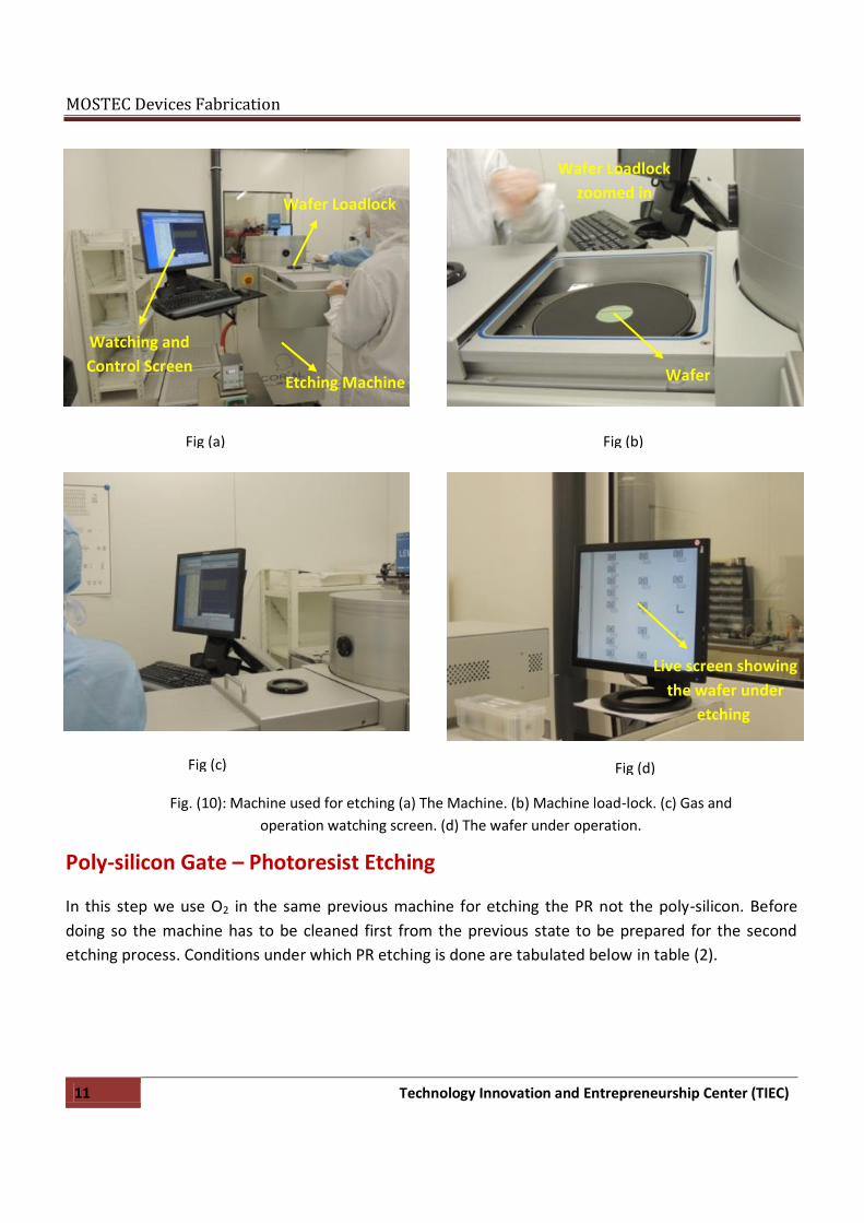
Dry etching RIE (Reactive Ion Etching)
Here the reactive ion etching is used to etch the poly-silicon layer. The Machine used in etching can be
seen in figure (10).
Figure (10,a) shows the Machine in which etching is done. Figure (10,c) shows the operating screen at
which the operator (the fab engineer) initialize the etching process, by defining gasses, watching the
current operation and also starts and ends the different processes letting gasses in and removing
gasses out of the operation region. And also the operator can see some curves for the whole operation
indicating the starting and ending of a specific process indicating that the etching process is done.
On the other hand, figure (10,d) shows the screen that watches the wafer under etching. Actually, the
wafer's color changes according to the material coating it, so by watching the wafer under etching
while it's being processed we can define accurately, by watching the wafer color, that the poly-silicon
has now been etched, not to over-etch the underlying field oxide or any other layer.
Gasses BCl3, Cl2, C2H4, SF6, CHF3, O2, Ar, He All gasses exist inside but only SF6 and Ar are used in etching
Pressure Starting at Vacuum 5 mtorr
Power 65 Watts
Etch Rate 90nm / 1.1min
Fig. (9): wafer cross-section after PR development over the poly-silicon layer
Table (1): Conditions under which poly etching is done (Gasses, Pressure, Power and
etching rate)
MOSTEC Devices Fabrication
11 Technology Innovation and Entrepreneurship Center (TIEC)
Poly-silicon Gate – Photoresist Etching
In this step we use O2 in the same previous machine for etching the PR not the poly-silicon. Before
doing so the machine has to be cleaned first from the previous state to be prepared for the second
etching process. Conditions under which PR etching is done are tabulated below in table (2).
Fig. (10): Machine used for etching (a) The Machine. (b) Machine load-lock. (c) Gas and
operation watching screen. (d) The wafer under operation.
Fig (a) Fig (b)
Fig (d) Fig (c)
Etching Machine
Watching and
Control Screen
Wafer Loadlock
Wafer Loadlock
zoomed in
Wafer
Live screen showing
the wafer under
etching

MOSTEC Devices Fabrication
12 Technology Innovation and Entrepreneurship Center (TIEC)
Gasses O2 for etching only PR
Pressure 100 mtorr
Power 150 Watt Bias voltage (back-side) is 550 Volts
Etching Rate 540 nm/min
Doping by Ion-Implantation
After building the poly-silicon gate we used it as a self-mask while doping the source and the drain by
ion implantation, as poly-silicon will protect the channel from being doped. The idea of ion
implantation is briefed in figure(11)
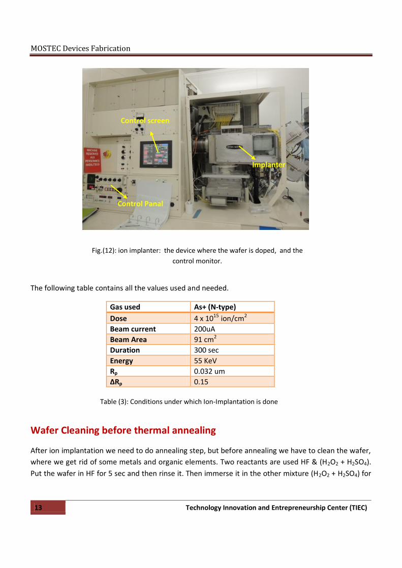
In this step we use a huge instrument for ion implantation which is shown in figure (12)
Table (2): Conditions under which PR etching is done (Gasses, Pressure, Power and
etching rate)
Fig.(11): ion implantation concept & device content
MOSTEC Devices Fabrication
13 Technology Innovation and Entrepreneurship Center (TIEC)
The following table contains all the values used and needed.
Gas used As+ (N-type)
Dose 4 x 10¹⁵ ion/cm2
Beam current 200uA
Beam Area 91 cm2
Duration 300 sec
Energy 55 KeV
Rp 0.032 um
ΔRp 0.15
Wafer Cleaning before thermal annealing
After ion implantation we need to do annealing step, but before annealing we have to clean the wafer,
where we get rid of some metals and organic elements. Two reactants are used HF & (H2O2 + H2SO4).
Put the wafer in HF for 5 sec and then rinse it. Then immerse it in the other mixture (H2O2 + H2SO4) for
Table (3): Conditions under which Ion-Implantation is done
Fig.(12): ion implanter: the device where the wafer is doped, and the
control monitor.
Implanter
Control Panal
Control screen
MOSTEC Devices Fabrication
14 Technology Innovation and Entrepreneurship Center (TIEC)
14 min at 120°C, then once more we immerse it in HF for 5 sec as to get rid from any oxide done by the
mixture, then rinse it once more. As usual after rinsing the wafer we do the dryer step.
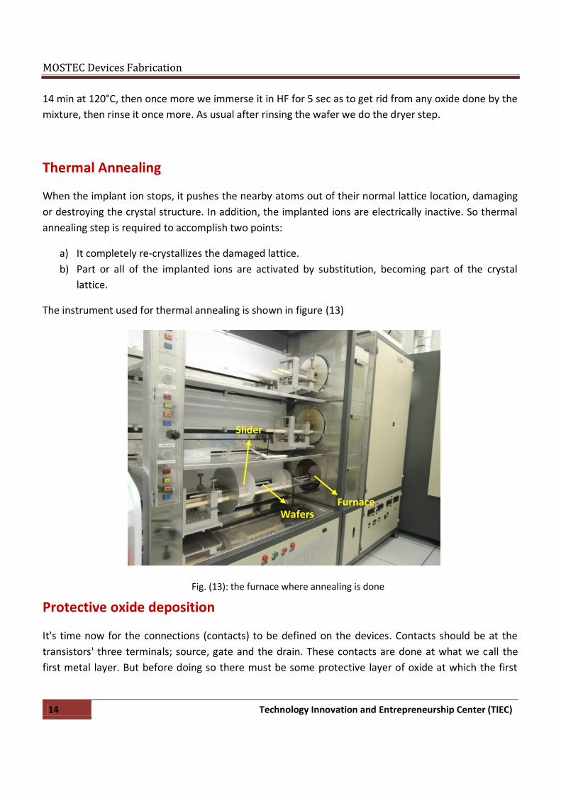
Thermal Annealing
When the implant ion stops, it pushes the nearby atoms out of their normal lattice location, damaging
or destroying the crystal structure. In addition, the implanted ions are electrically inactive. So thermal
annealing step is required to accomplish two points:
a) It completely re-crystallizes the damaged lattice.
b) Part or all of the implanted ions are activated by substitution, becoming part of the crystal
lattice.
The instrument used for thermal annealing is shown in figure (13)
Protective oxide deposition
It's time now for the connections (contacts) to be defined on the devices. Contacts should be at the
transistors' three terminals; source, gate and the drain. These contacts are done at what we call the
first metal layer. But before doing so there must be some protective layer of oxide at which the first
Fig. (13): the furnace where annealing is done
Furnace Wafers
Slider

MOSTEC Devices Fabrication
15 Technology Innovation and Entrepreneurship Center (TIEC)
metal layer is going to be built on. This is done through what we call Plasma Enhanced Chemical Vapor
Deposition. Figure (14) shows the wafer after the deposition process.
This process is done by the same machine of etching described in figure(10). A think oxide layer is
deposited over the whole silicon wafer. A summarizing table for the operation can be seen in table(4).
Gasses SiH4, N2O
Pressure 1800 mTorr
Power 280 Watt
Deposition Rate 260 nm/minute
Targeted Thickness 300
Protective oxide photolithography
This is done exactly the same as the previously done photolithography process. Figure(15) shows the
wafer after the PR development.
Fig. (14): The wafer cross-section after the deposition process
Fig. (15): The wafer cross-section after the PR Development
Table(4): Conditions under which deposition process is done

MOSTEC Devices Fabrication
16 Technology Innovation and Entrepreneurship Center (TIEC)
Aluminum contact - sputtering
As we can see in figure (15) the contacts places are ready for the metal to be deposited on the wafer
for filling in the places we opened previously. These are the contacts that we will use after that for the
electrical testing. Figure (16) shows the machine used for sputtering the aluminum.
The conditions under which the sputtering is done are tabulated in table (5).
Gasses Ar+
Pressure 10^-2 mTorr
Power 1000 Watts
Deposition Rate 600 nm/150sec
Targeted Thickness 600 nm
Duration time 150 sec
Fig. (16): Machine used for Aluminum Sputtering
Table (5): Conditions under which Aluminum Sputtering is done
Plasma Chamber
MOSTEC Devices Fabrication
17 Technology Innovation and Entrepreneurship Center (TIEC)
Aluminum contact - photolithography
Now, we have to do photolithography for defining the contact places on the Aluminum we've just
sputtered all over the wafer. This is done also the same as the previously done photolithography
process
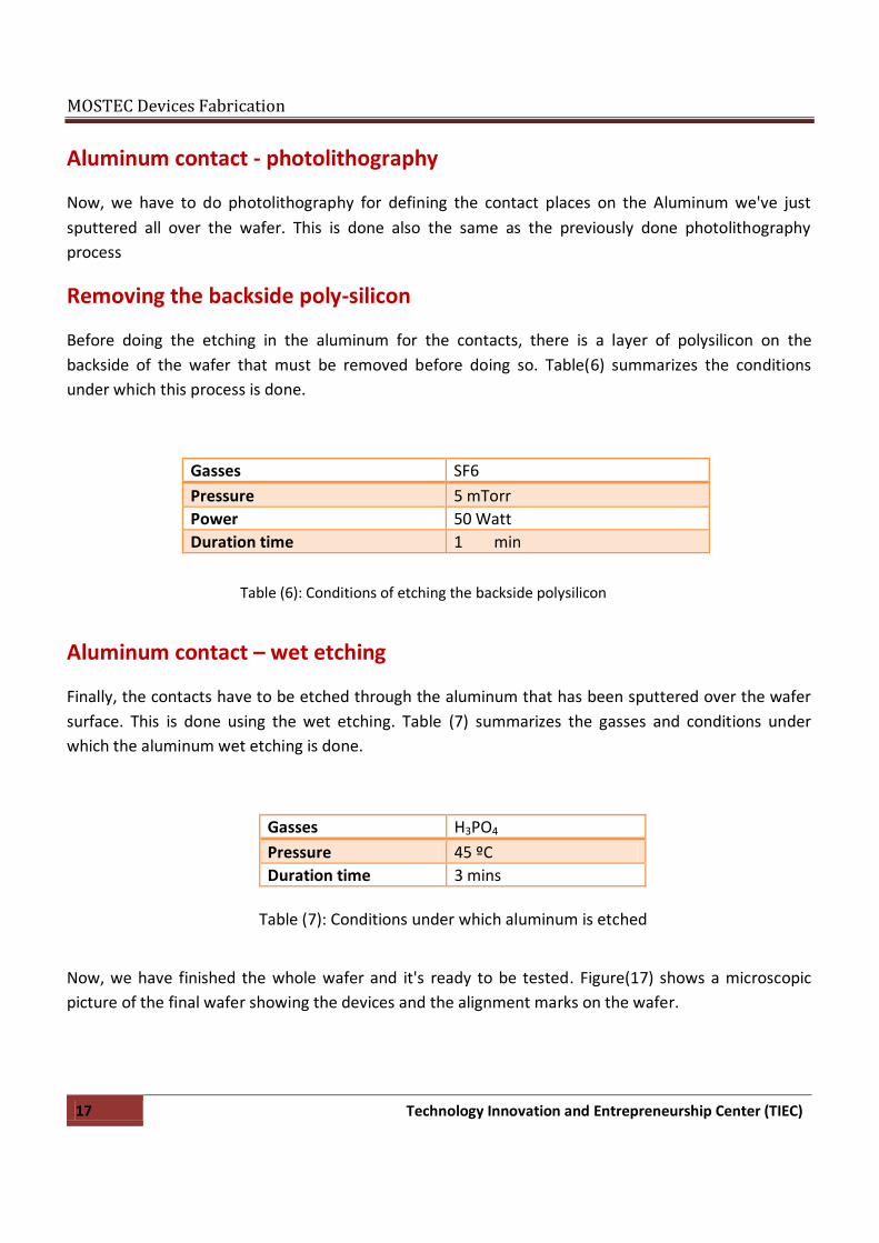
Removing the backside poly-silicon
Before doing the etching in the aluminum for the contacts, there is a layer of polysilicon on the
backside of the wafer that must be removed before doing so. Table(6) summarizes the conditions
under which this process is done.
Gasses SF6
Pressure 5 mTorr
Power 50 Watt
Duration time 1 min
Aluminum contact – wet etching
Finally, the contacts have to be etched through the aluminum that has been sputtered over the wafer
surface. This is done using the wet etching. Table (7) summarizes the gasses and conditions under
which the aluminum wet etching is done.
Gasses H3PO4
Pressure 45 ºC
Duration time 3 mins
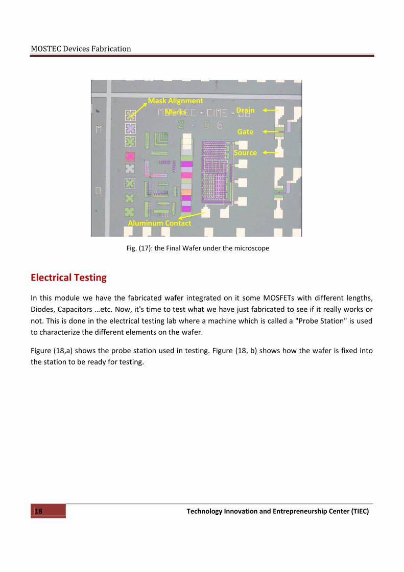
Now, we have finished the whole wafer and it's ready to be tested. Figure(17) shows a microscopic
picture of the final wafer showing the devices and the alignment marks on the wafer.
Table (6): Conditions of etching the backside polysilicon
Table (7): Conditions under which aluminum is etched
MOSTEC Devices Fabrication
18 Technology Innovation and Entrepreneurship Center (TIEC)
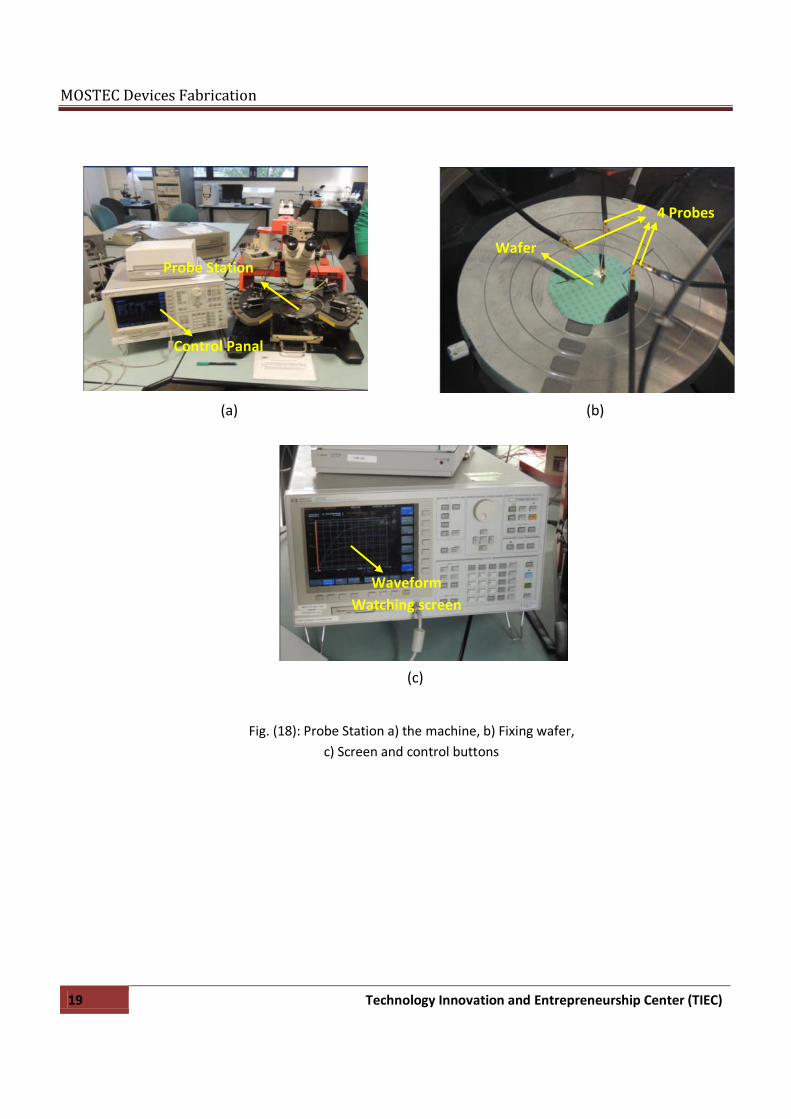
Electrical Testing
In this module we have the fabricated wafer integrated on it some MOSFETs with different lengths,
Diodes, Capacitors …etc. Now, it's time to test what we have just fabricated to see if it really works or
not. This is done in the electrical testing lab where a machine which is called a "Probe Station" is used
to characterize the different elements on the wafer.
Figure (18,a) shows the probe station used in testing. Figure (18, b) shows how the wafer is fixed into
the station to be ready for testing.
Fig. (17): the Final Wafer under the microscope
Mask Alignment
Marks
Aluminum Contact
Drain
Gate
Source
MOSTEC Devices Fabrication
19 Technology Innovation and Entrepreneurship Center (TIEC)
(a)
Fig. (18): Probe Station a) the machine, b) Fixing wafer,
c) Screen and control buttons
(b)
(c)
Control Panal
Probe Station Wafer
4 Probes
Waveform
Watching screen

MOSTEC Devices Fabrication
20 Technology Innovation and Entrepreneurship Center (TIEC)
Finally, Figure (19) shows some of the characteristic curves that has been observed.
Silvaco TCAD tools
We are using some programs (Silvaco TCAD tools) to simulate accurately the previous process plus the
characteristic of the device. We use ATHENA as process simulation framework and ATLAS as device
simulation framework.
ATHENA framework integrates several process simulation modules within a user-friendly environment.
It provides a convenient platform for simulating processes used in semiconductor industry: ion
implantation, diffusion, oxidation, physical etching and deposition, lithography, stress formation and
silicidation.
We used ATHENA to implement all the previous process had mentioned before, where it helped us to
use some commands to write a code to create our MOS device, the resulted output is shown in
figure(20 a&b)
Fig. (19): Results out of the testing of the MOSFETs (a)
Ids-Vds Curve, (b) Ids-Vds and Gm Curves.
(a) (b)
Fig. (20) Silvaco outputs a) the NMOS b) NMOS when
selecting doping contour
(a) (b)

MOSTEC Devices Fabrication
21 Technology Innovation and Entrepreneurship Center (TIEC)
ATLAS enables device technology engineers to simulate the electrical, optical, and thermal behavior of
semiconductor devices. ATLAS provides a physics-based, easy to use, modular, and extensible platform
to analyze DC, AC, and time domain responses for all semiconductor based technologies in 2 and 3
dimensions.
By using atlas, we used the ATHENA output file to do all the characteristics on it, and to draw any
curves and relations we need.
Course Organization
In this section we’re going to show how the course has been organized through the whole journey. The
course was divided into 3 modules:
Module (1): Clean Rooms Technology Process for CMOS Fabrication
This module is divided into 5 sessions:
Session (1): photolithography of field oxide, wet etching and removal of PR processes
are done in this session.
Session (2): Poly-silicon Gate processes are accomplished in this session.
Session (3): At which Ion-Implantation, Wafer cleaning and Thermal Annealing are done.
Session (4): Protective oxide is done here.
Session (5): Aluminum Contact finally is done here.
Module (2): Device Characterization & Electrical Characterization of CMOS Devices
In this module the device characterization ( e.g. Vth calculation, Mobility …..etc. ) and the
electrical characterization(e.g. I-V Curves …..etc. ) of the CMOS devices (e.g. Caps, Diodes and
Transistors )are done.
Module (3): Modeling using Technology Computer Aided Design
In this module the whole process of fabrication are written in computer software (Silvaco) and
simulated.
MOSTEC Devices Fabrication
22 Technology Innovation and Entrepreneurship Center (TIEC)
Conclusion
This paper shows a brief description of the IC fabrication grant provided by TIEC. It reflects the
knowledge and experience of the grant candidates gained through whole course. The fabrication
process is described from the very beginning till the chip testing. Each step of fabrication is described
briefly with the process conditions. Photos are attached in the paper for clearing precisely the process
and the machines used in fabrication process.
As this course proves success, we seek of initiating more and more such courses helping in the IC
fabrication and design developing in Egypt.
Related Documents