Lab Assignment No. 1 AIM: TO STUDY THE CHARACTERISTICS OF Id AND Vgs ABSTRACT The main aim of this experiment is to plot the Vgs v/s Id characteristics and observe the effect on the drain current when Vgs is varied. Further the device parameters such as the mobility and the channel length are varied to observe the effect on the characteristics. THEORY - The equation used in this experiment is- Id=(1/2)*µ n *Cox*(W/L)*(Vgs-Vth) 2 Where Id= drain current, µ n = mobility of electrons, Cox= oxide capacitance,W= width of the MOSFET, L= channel length , Vgs= gate source voltage, Vth= threshold voltage. The above equation is valid when the MOSFET is in saturation where the drain current no longer depends on the drain to source voltage but it rather follows the square law. MATLAB CODE- a) When µ n is varied- clc; clear all; close all; Vgs=[0:.5:30]; Vt=.4; Mn1=300*(10^(-4)); Mn2=500*(10^(-4)); Mn3=700*(10^(-4)); Cox=((3.9*8.854*(10^(-3)))/2); W=10^(-9); L=(10^(-7)) for i=1:length(Vgs) Id1(i)=(0.5*Mn1*Cox*W*((Vgs(i)-Vt)^2)/L); Id2(i)=(0.5*Mn2*Cox*W*((Vgs(i)-Vt)^2)/L); Id3(i)=(0.5*Mn3*Cox*W*((Vgs(i)-Vt)^2)/L); end plot(Vgs,Id1,'Color',[.6 0 0]);grid; hold on; plot(Vgs,Id2,'Color',[0 .6 0]);grid; hold on; plot(Vgs,Id3,'Color',[0 0 .6]);grid; hold on;

Welcome message from author
This document is posted to help you gain knowledge. Please leave a comment to let me know what you think about it! Share it to your friends and learn new things together.
Transcript
Lab Assignment No. 1
AIM: TO STUDY THE CHARACTERISTICS OF Id AND Vgs
ABSTRACT
The main aim of this experiment is to plot the Vgs v/s Id characteristics andobserve the effect on the drain current when Vgs is varied. Further the deviceparameters such as the mobility and the channel length are varied to observe the effecton the characteristics.
THEORY -
The equation used in this experiment is-
Id=(1/2)*µn*Cox*(W/L)*(Vgs-Vth)2
Where Id= drain current, µn = mobility of electrons, Cox= oxide capacitance,W= width ofthe MOSFET, L= channel length , Vgs= gate source voltage, Vth= threshold voltage.
The above equation is valid when the MOSFET is in saturation where the drain currentno longer depends on the drain to source voltage but it rather follows the square law.
MATLAB CODE-
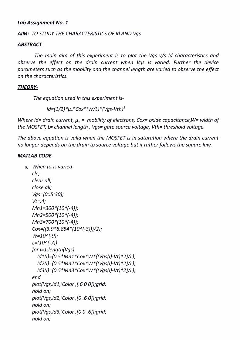
a) When µn is varied-clc;clear all;close all;Vgs=[0:.5:30];Vt=.4;Mn1=300*(10^(-4));Mn2=500*(10^(-4));Mn3=700*(10^(-4));Cox=((3.9*8.854*(10^(-3)))/2);W=10^(-9);L=(10^(-7))for i=1:length(Vgs) Id1(i)=(0.5*Mn1*Cox*W*((Vgs(i)-Vt)^2)/L); Id2(i)=(0.5*Mn2*Cox*W*((Vgs(i)-Vt)^2)/L); Id3(i)=(0.5*Mn3*Cox*W*((Vgs(i)-Vt)^2)/L);endplot(Vgs,Id1,'Color',[.6 0 0]);grid;hold on;plot(Vgs,Id2,'Color',[0 .6 0]);grid;hold on;plot(Vgs,Id3,'Color',[0 0 .6]);grid;hold on;
xlabel ('Vgs (V)---------------->');ylabel ('Id (A)---------------->');
Schematic matlab output-
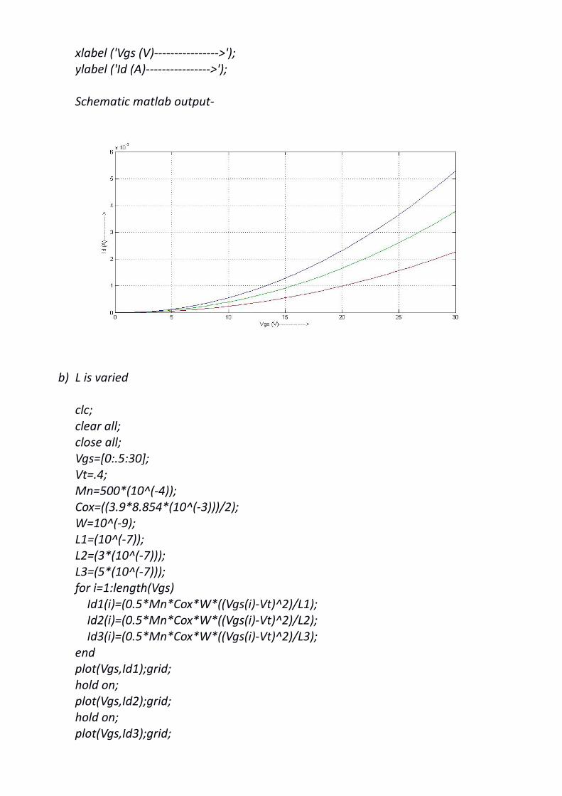
b) L is varied
clc;clear all;close all;Vgs=[0:.5:30];Vt=.4;Mn=500*(10^(-4));Cox=((3.9*8.854*(10^(-3)))/2);W=10^(-9);L1=(10^(-7));L2=(3*(10^(-7)));L3=(5*(10^(-7)));for i=1:length(Vgs) Id1(i)=(0.5*Mn*Cox*W*((Vgs(i)-Vt)^2)/L1); Id2(i)=(0.5*Mn*Cox*W*((Vgs(i)-Vt)^2)/L2); Id3(i)=(0.5*Mn*Cox*W*((Vgs(i)-Vt)^2)/L3);endplot(Vgs,Id1);grid;hold on;plot(Vgs,Id2);grid;hold on;plot(Vgs,Id3);grid;
hold on;xlabel('Vgs (V)---------------->');ylabel('Id (A)---------------->');
OUTPUT-
CONCLUSION- As observed from the two output graph that with changes in themobility as well as the channel length, the drain current shows a variation withincrease in the gate source voltage. As the mobility of carriers increases, the draincurrent increases. This is because, increase of mobility signifies that there are lesscollision and electrons can move through the channel freely and hence generatemore current. With the decrease in channel length, the current increases. Becausea shorter channel has more concentration of carriers and more carrierconcentration will generate more current.
Lab Assignment No 2AIM - TO OBSERVE THE VARIATION OF TRANSCONDUCTANCE W.R.T. THE DRAINCURRENT AND THE OVERDRIVE VOLTAGE.
ABSTRACTIn this experiment we will determine the variation of the transconductance
of the MOSFET with the drain current Id as well as the overdrive voltage (Vgs-Vth).
THEORY We all know that a MOSFET operating in saturation always produces a
constant current in response to the variation of gate source voltage. That is italways behaves like a current source. Transconductance is the measure of howwell the MOSFET device is able to convert the voltage into output current. Thegoverning equations are-1) gm= µn*Cox*(W/L)*(Vgs-Vth) A/V; where gm is the transconductance of the
device, µn is the mobility of carriers, Cox is the oxide capacitance, W= width ofthe device, L=channel length, (Vgs-Vth)= overdrive voltage.
2) gm= √2µ n∗Cox∗ (W /L ) Id A/V; Id is the drain current.3) gm= (2*Id)/(Vgs-Vth) A/V.
MATLAB CODE-1) clc; clear all; close all;
Vgs=[0:0.5:10];Vt=0.7;Mn=(500*10^(-4));Cox=(3.9*8.854*10^(-3)/2);W=10^-9;L=10^-7;for i=1:length(Vgs)
gm(i)=((Mn*Cox*W*(Vgs(i)-Vt))/L); endfor i=1:length(Vgs)
t(i)=Vgs(i)-Vt;endplot(t,gm);grid;title('Graph of (Vgs-Vt) v/s gm');
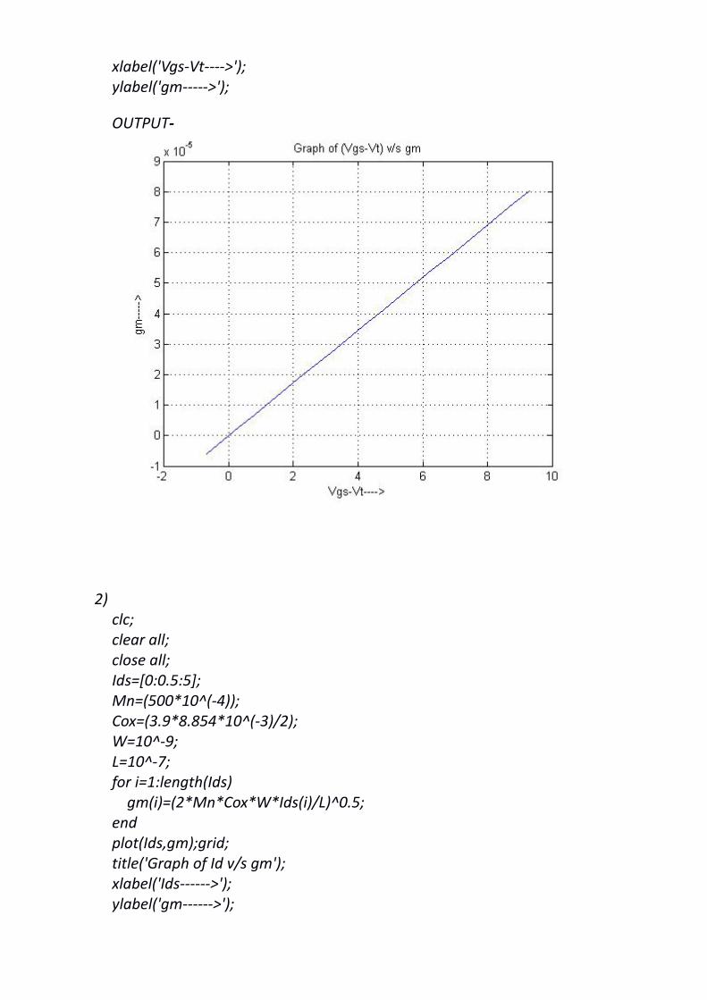
xlabel('Vgs-Vt---->');ylabel('gm----->');
OUTPUT-
2)clc;clear all;close all;Ids=[0:0.5:5];Mn=(500*10^(-4));Cox=(3.9*8.854*10^(-3)/2);W=10^-9;L=10^-7;for i=1:length(Ids) gm(i)=(2*Mn*Cox*W*Ids(i)/L)^0.5;endplot(Ids,gm);grid;title('Graph of Id v/s gm');xlabel('Ids------>');ylabel('gm------>');
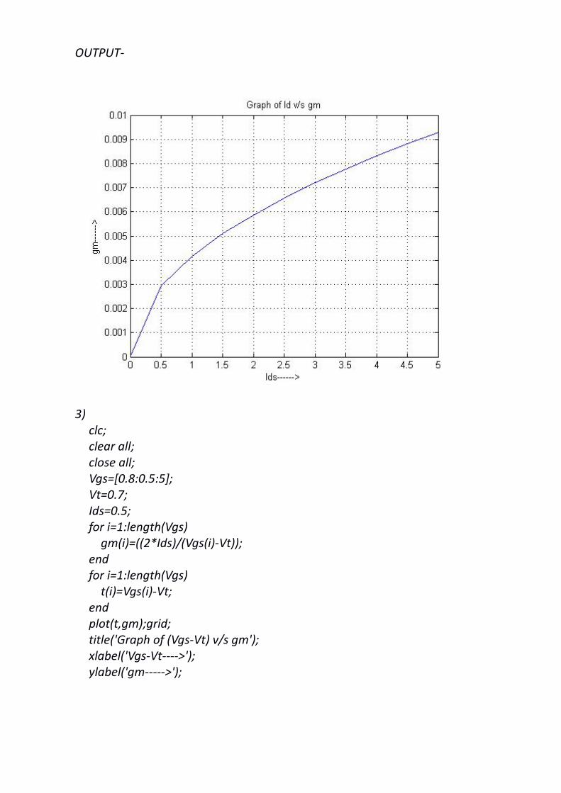
OUTPUT-
3)clc;clear all;close all;Vgs=[0.8:0.5:5];Vt=0.7;Ids=0.5;for i=1:length(Vgs) gm(i)=((2*Ids)/(Vgs(i)-Vt));endfor i=1:length(Vgs) t(i)=Vgs(i)-Vt;endplot(t,gm);grid;title('Graph of (Vgs-Vt) v/s gm');xlabel('Vgs-Vt---->');ylabel('gm----->');
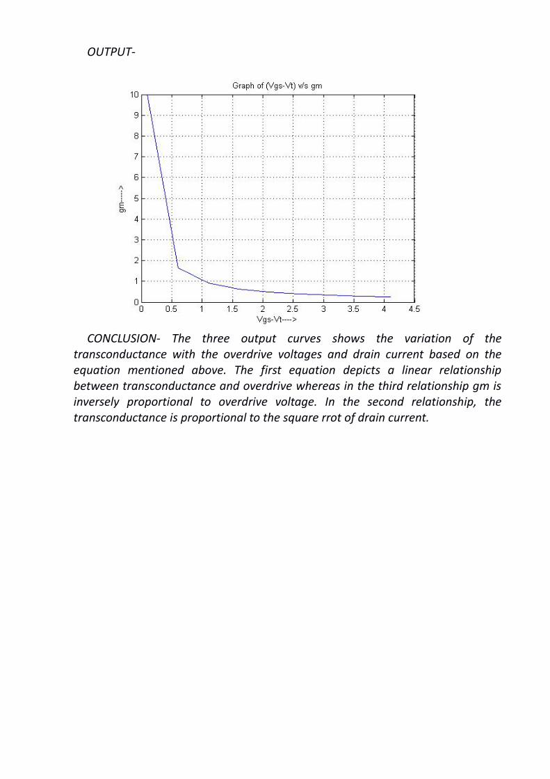
OUTPUT-
CONCLUSION- The three output curves shows the variation of thetransconductance with the overdrive voltages and drain current based on theequation mentioned above. The first equation depicts a linear relationshipbetween transconductance and overdrive whereas in the third relationship gm isinversely proportional to overdrive voltage. In the second relationship, thetransconductance is proportional to the square rrot of drain current.
Lab Assignment No 3AIM - TO STUDY THE VARIATION OF THE CHARGE IN THE DEPLETED REGIONWITH VOLTAGE AT ANY POINT x ALONG THE CHANNEL.
ABSTRACT- The aim of this experiment is to observe how the charge density along
along the varies with the voltage at any point x along the channel and vice versa.
THEORY The equations used in this experiment are given below-
Qd(x)=WCox(Vgs-V(x)-Vth) C;Where Qd(x) is the charge density at any point x along the channel, V(x) is the voltageat any point x.To observe the reverse case, i.e., the variation of Vx w.r.t. to Qd the following equation isused-
Vx=(Vgs-Vth)-(Qd/WCox) V.
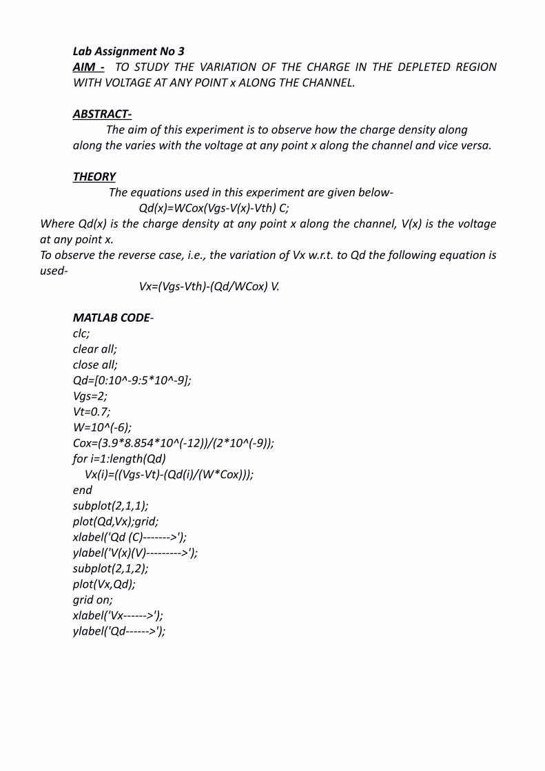
MATLAB CODE- clc;clear all;close all;Qd=[0:10^-9:5*10^-9];Vgs=2;Vt=0.7;W=10^(-6);Cox=(3.9*8.854*10^(-12))/(2*10^(-9));for i=1:length(Qd) Vx(i)=((Vgs-Vt)-(Qd(i)/(W*Cox)));endsubplot(2,1,1);plot(Qd,Vx);grid;xlabel('Qd (C)------->');ylabel('V(x)(V)--------->');subplot(2,1,2);plot(Vx,Qd);grid on;xlabel('Vx------>');ylabel('Qd------>');
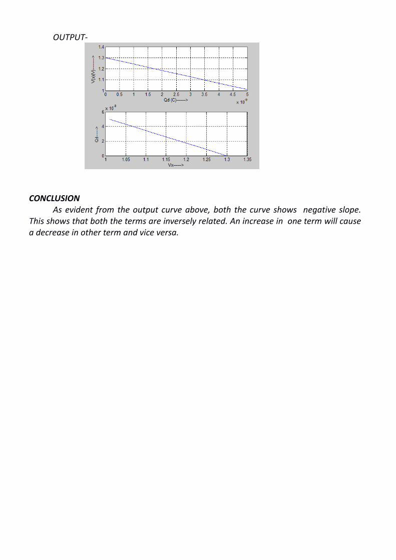
OUTPUT-
CONCLUSION As evident from the output curve above, both the curve shows negative slope.
This shows that both the terms are inversely related. An increase in one term will causea decrease in other term and vice versa.
Lab Assignment no. 4
AIM: To study the characteristics of Id with varying parameters, considering both Triode
and Saturation region.
ABSTRACT:
In this experiment the graph of Id is plotted with varying the parameters like- length (L),
Vgs in the Saturation region as well in Triode region.
THEORY:
a) Triode region:When the Gate voltage is in the range 0<Vgs<Vt, the gated region between the
source and drain is depleted. No carrier flow can be observed in the channel. As
the gate voltage is increased beyond the threshold voltage (Vgs > Vt), an
inversion layer is formed. Thus, in linear region operation, the channel region acts as a voltage-controlled
resistor.The output current Id for the triode region id given by:
Id= (0.5*Un*Cox*W)/L*[2*(Vgs-Vt)*Vds-Vds2]
b) Saturation region:For Vds = Vdsat, the inversion charge at the drain is reduced to zero, which is
called the pinch-off point. Beyond the pinch-off point, a depleted surface region
forms adjacent to the drain, and this depletion region grows toward the source
with increasing drain voltages. This operation mode of the MOSFET is called the
saturation mode or the saturation region. In the saturation region the current
equation for Id is given by:
Id= (0.5*Un*Cox*W)/L*(Vgs-Vt)2
MATLAB CODE:c) Triode region:
clc;clear all;u=500*10^(-4);
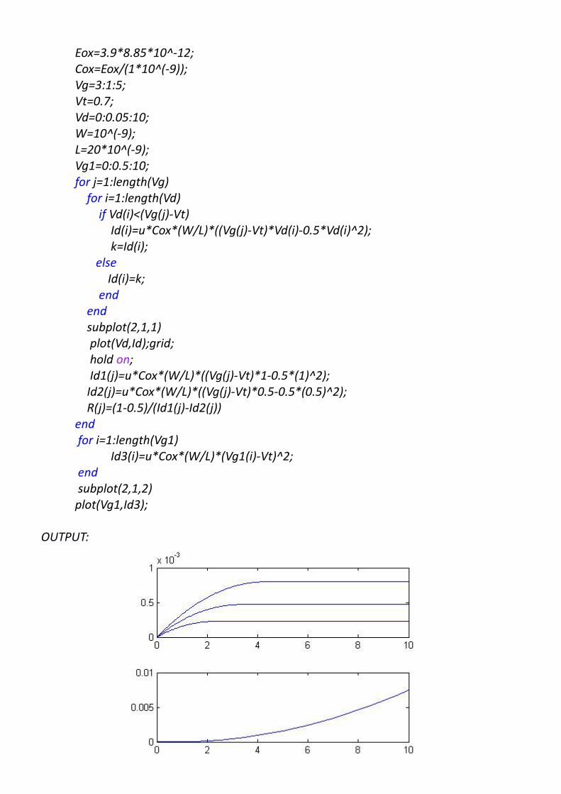
Eox=3.9*8.85*10^-12;Cox=Eox/(1*10^(-9));Vg=3:1:5;Vt=0.7;Vd=0:0.05:10;W=10^(-9);L=20*10^(-9);Vg1=0:0.5:10;for j=1:length(Vg) for i=1:length(Vd) if Vd(i)<(Vg(j)-Vt) Id(i)=u*Cox*(W/L)*((Vg(j)-Vt)*Vd(i)-0.5*Vd(i)^2); k=Id(i); else Id(i)=k; end end subplot(2,1,1) plot(Vd,Id);grid; hold on; Id1(j)=u*Cox*(W/L)*((Vg(j)-Vt)*1-0.5*(1)^2); Id2(j)=u*Cox*(W/L)*((Vg(j)-Vt)*0.5-0.5*(0.5)^2); R(j)=(1-0.5)/(Id1(j)-Id2(j))end for i=1:length(Vg1) Id3(i)=u*Cox*(W/L)*(Vg1(i)-Vt)^2; end subplot(2,1,2)plot(Vg1,Id3);
OUTPUT:
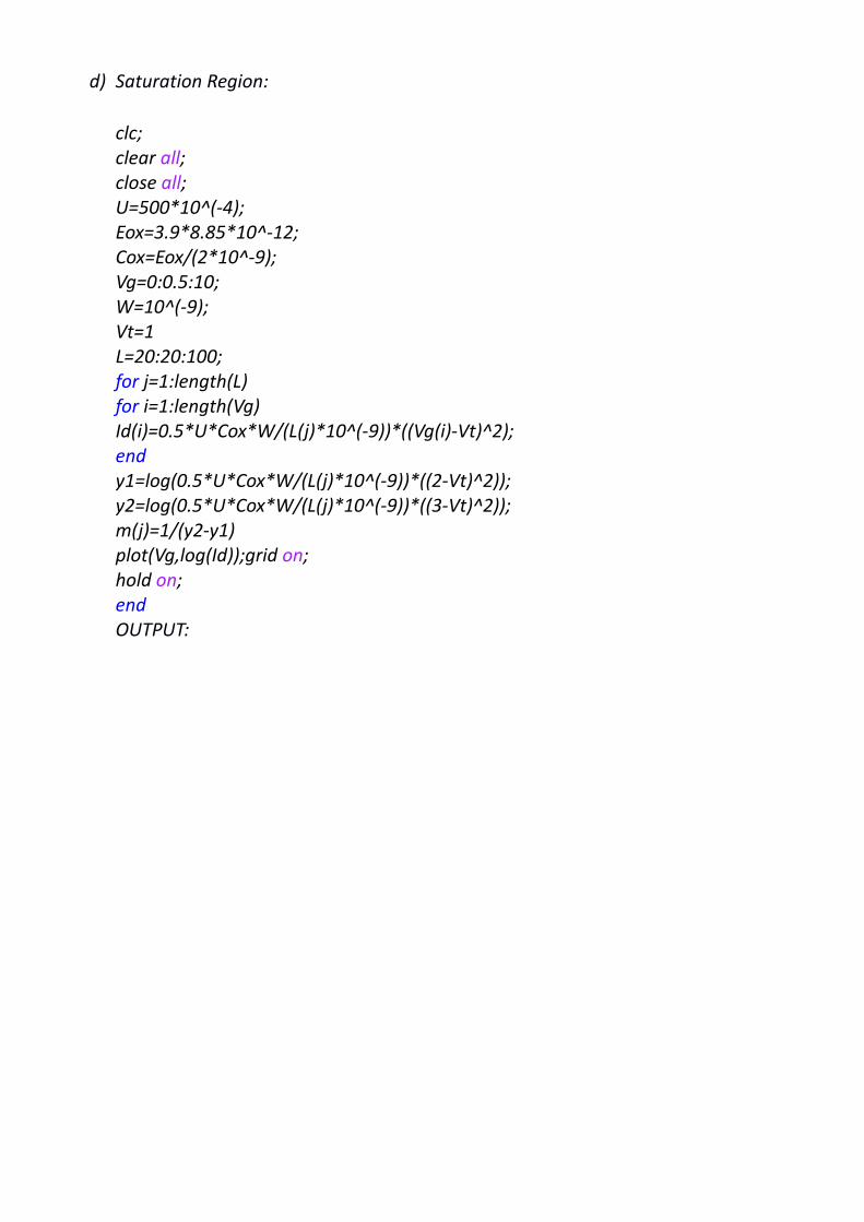
d) Saturation Region:
clc;clear all;close all;U=500*10^(-4);Eox=3.9*8.85*10^-12;Cox=Eox/(2*10^-9);Vg=0:0.5:10;W=10^(-9);Vt=1L=20:20:100;for j=1:length(L)for i=1:length(Vg)Id(i)=0.5*U*Cox*W/(L(j)*10^(-9))*((Vg(i)-Vt)^2);endy1=log(0.5*U*Cox*W/(L(j)*10^(-9))*((2-Vt)^2));y2=log(0.5*U*Cox*W/(L(j)*10^(-9))*((3-Vt)^2));m(j)=1/(y2-y1)plot(Vg,log(Id));grid on;hold on;endOUTPUT:
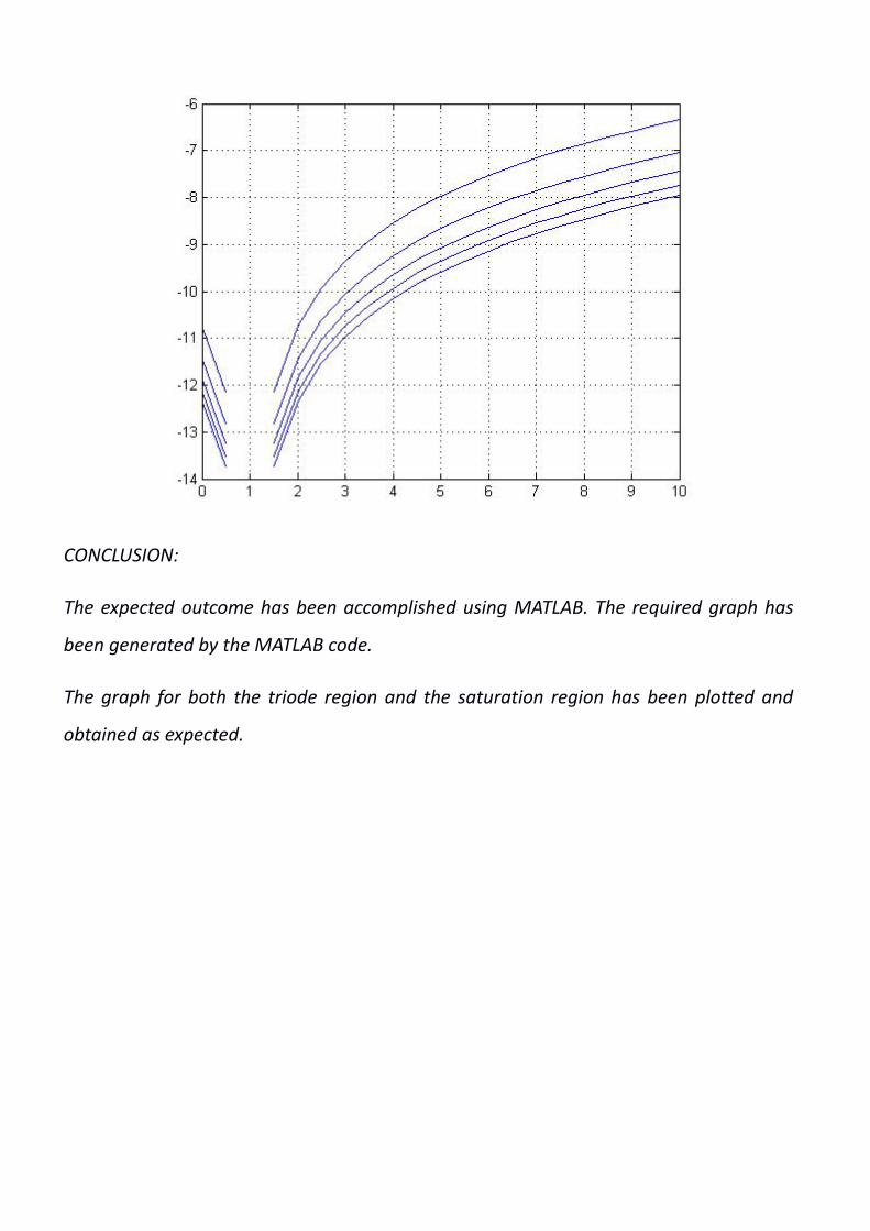
CONCLUSION:
The expected outcome has been accomplished using MATLAB. The required graph has
been generated by the MATLAB code.
The graph for both the triode region and the saturation region has been plotted and
obtained as expected.
Lab Assignment No 5
AIM: To implement the CS configuration
Abstract:
In this experiment we have study the behavior of transconductance, outputimpedance, intrinsic gain and output voltage with respect to the input voltage andplotted the graph correspondingly.
Theory:
We know that the equation of drain current is -
Id=0.5*Un*Cox*WL*(Vin-Vt)^2
Equation of output voltage is given as-
Vo=Vdd-Rd*Id1
Equation of transconductance is-
gm= √(2∗Un∗Cox∗ (W /L)∗ Id )
Equation of output impedance is-
ro=1/(Un*Cox*WL*(Vin-Vt))
MATLAB CODE:
c) To draw the graph of gm,Id and Vout with respect to Vin
Rd=1000;
MnCox=50*10^-6;
WL=10;
for i=1:length(Vin)
if Vin(i)<=Vt
Vo(i)=Vdd;
elseif ((Vin(i)>Vt) && (Vin(i)<4))
Id1(i)=0.5*MnCox*WL*(Vin(i)-Vt)^2;
Vo(i)=Vdd-Rd*Id1(i);
gm(i)=((2*MnCox*WL*Id1(i))^0.5);
elseif (Vin(i)>=4)
% Id2(j)=0.5*u*Cox*((2*Vin(i)-Vt)*Vo(i-1)-Vo(i-1)^2);
%Vo(i)=Vdd-Rd*Id2(j);
% j=j+1;
Ron(i)=1/(MnCox*WL*(Vin(i)-Vt));
Vo(i)=(Vdd*Ron(i))/(Ron(i)+Rd);
Id1(i)=Vdd/(Rd+Ron(i));
gm(i)=(MnCox*WL*Vo(i-1));
end
end
subplot(3,1,1)
plot(Vin,Vo);
grid on;
xlabel('Vin----->');
ylabel('Vout---->');
subplot(3,1,2)
plot(Vin,Id1);
grid on;
xlabel('Vin---->');
ylabel('Id----->');
subplot(3,1,3)
plot(Vin,gm);
grid on;
xlabel('Vin---->');
ylabel('gm------>');
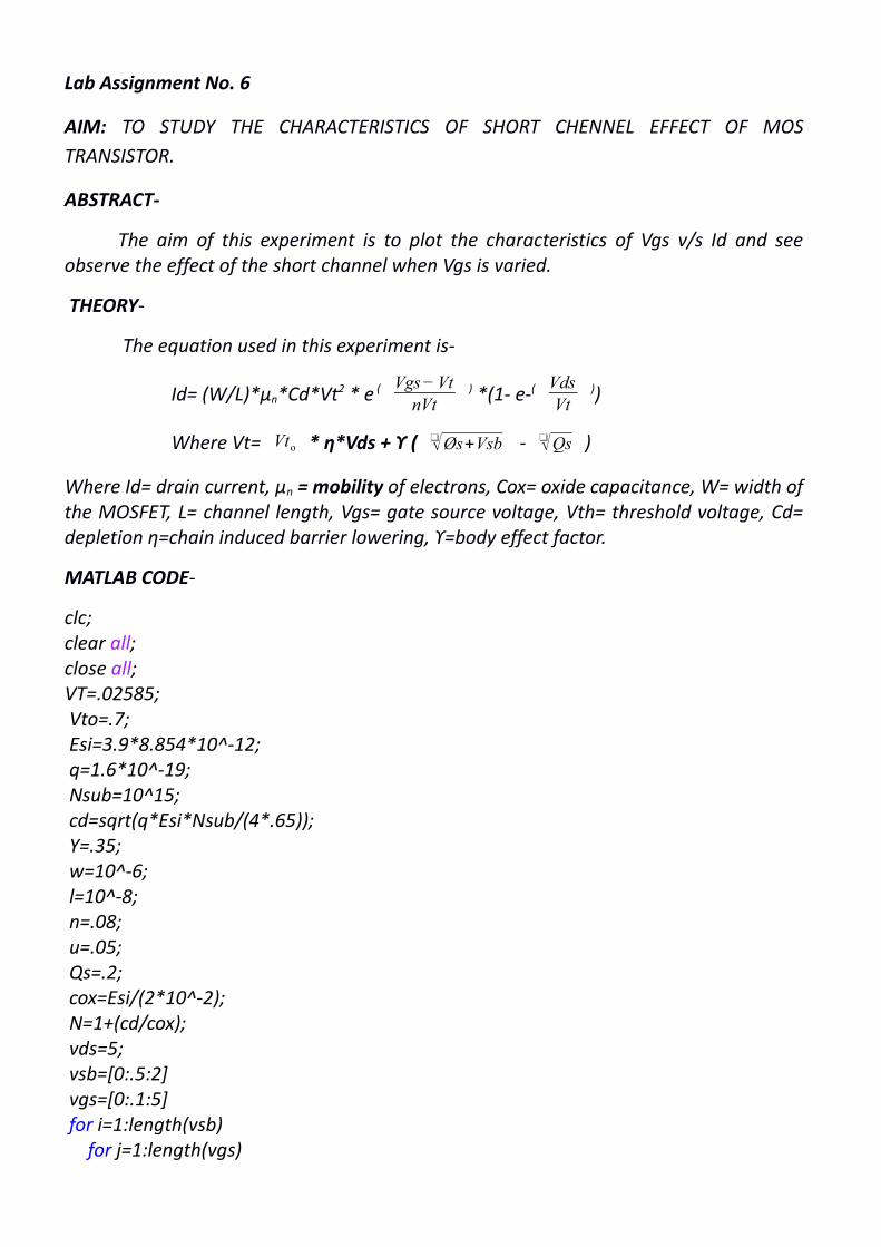
d) To obtain the graph between ro vs L and Id vs Vds
clc;clear all;
close all;Vds=[0:0.05:2.5];Vt=0.7;Vgs=3;Mn=1000*10^(-4);Eox=3.9*8.854*10^(-12);tox=10^(-9);Cox=Eox/tox;L=[2*10^(-8):2*10^(-8):10*10^(-8)];W=10^-6;subplot(2,1,1);for j=1:length(L) for i=1:length(Vds) Id(i)=(Mn*Cox*W*(((Vgs-Vt)*Vds(i))-(Vds(i)^(2)/2))/L(j)); end plot(Vds,Id); grid; hold on;endfor m=1:length(L) Vds=2.3 Id1(m)=(Mn*Cox*W*(((Vgs-Vt)*Vds)-(Vds^(2)/2))/L(m)); Vds=2.29 Id2(m)=(Mn*Cox*W*(((Vgs-Vt)*Vds)-(Vds^(2)/2))/L(m));endfor k=1:length(L) R(k)=0.01/(Id1(k)-Id2(k));endsubplot(2,1,2);plot(L,R);grid;hold on;
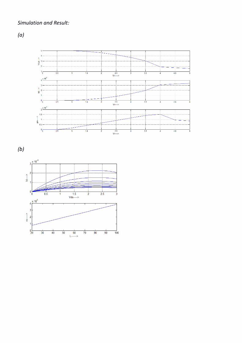
Simulation and Result:
(a)
(b)
Lab Assignment No. 6
AIM: TO STUDY THE CHARACTERISTICS OF SHORT CHENNEL EFFECT OF MOSTRANSISTOR.
ABSTRACT-
The aim of this experiment is to plot the characteristics of Vgs v/s Id and seeobserve the effect of the short channel when Vgs is varied.
THEORY-
The equation used in this experiment is-
Id= (W/L)*µn*Cd*Vt2 * e ( Vgs−VtnVt
) *(1- e-( VdsVt
))
Where Vt= Vto * η*Vds + ϒ ( ❑√Øs+Vsb - ❑√Qs )
Where Id= drain current, µn = mobility of electrons, Cox= oxide capacitance, W= width ofthe MOSFET, L= channel length, Vgs= gate source voltage, Vth= threshold voltage, Cd=depletion η=chain induced barrier lowering, ϒ=body effect factor.
MATLAB CODE-
clc;clear all;close all;VT=.02585; Vto=.7; Esi=3.9*8.854*10^-12; q=1.6*10^-19; Nsub=10^15; cd=sqrt(q*Esi*Nsub/(4*.65)); Y=.35; w=10^-6; l=10^-8; n=.08; u=.05; Qs=.2; cox=Esi/(2*10^-2); N=1+(cd/cox); vds=5; vsb=[0:.5:2] vgs=[0:.1:5] for i=1:length(vsb) for j=1:length(vgs)
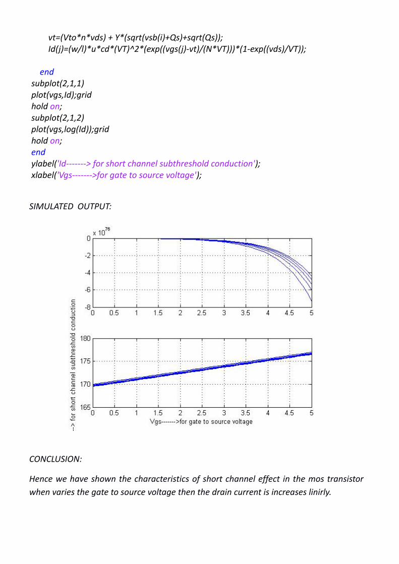
vt=(Vto*n*vds) + Y*(sqrt(vsb(i)+Qs)+sqrt(Qs)); Id(j)=(w/l)*u*cd*(VT)^2*(exp((vgs(j)-vt)/(N*VT)))*(1-exp((vds)/VT)); end subplot(2,1,1) plot(vgs,Id);grid hold on; subplot(2,1,2) plot(vgs,log(Id));grid hold on; end ylabel('Id-------> for short channel subthreshold conduction'); xlabel('Vgs------->for gate to source voltage');
SIMULATED OUTPUT:
CONCLUSION:
Hence we have shown the characteristics of short channel effect in the mos transistorwhen varies the gate to source voltage then the drain current is increases linirly.
Related Documents


