Digital Integrated Circuits © Prentice Hall 1995 Introduction MOS Transistor

Welcome message from author
This document is posted to help you gain knowledge. Please leave a comment to let me know what you think about it! Share it to your friends and learn new things together.
Transcript
Digital Integrated Circuits © Prentice Hall 1995Introduction
MOS Transistor

Digital Integrated Circuits © Prentice Hall 1995Introduction
MOS Structure
( Two Terminal MOS Structure )

Digital Integrated Circuits © Prentice Hall 1995Introduction
Metal Oxide(Sio2) Semiconductor
MOS Structure
( Energy band diagram for Metal, Oxide(Sio2) and
Semiconductor )

Digital Integrated Circuits © Prentice Hall 1995Introduction
MOS Structure

Digital Integrated Circuits © Prentice Hall 1995Introduction
( Energy band diagram of Combined MOS system )
E0
E0
E0 E0
MOS Structure

Digital Integrated Circuits © Prentice Hall 1995Introduction
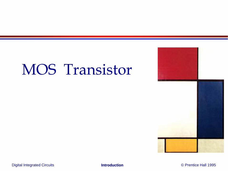
MOS System under External Bias
Digital Integrated Circuits © Prentice Hall 1995Introduction
MOS System under External Bias

Digital Integrated Circuits © Prentice Hall 1995Introduction
MOS System under External Bias
( N MOS operating in surface inversion region )
Digital Integrated Circuits © Prentice Hall 1995Introduction
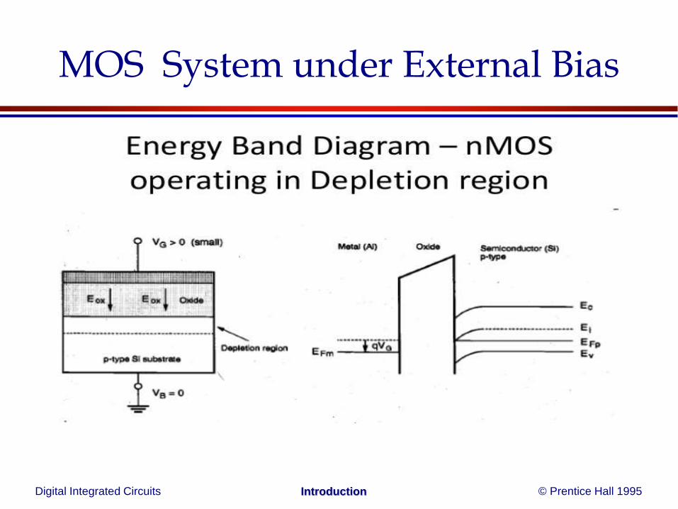
Structure and Operation of MOSFET
( N channel Enhancement MOSFET )

Digital Integrated Circuits © Prentice Hall 1995Introduction
Structure and Operation of MOSFET

Digital Integrated Circuits © Prentice Hall 1995Introduction
Structure and Operation of MOSFET
( Formation of Depletion Region in N type
Enhancement type MOSFET )

Digital Integrated Circuits © Prentice Hall 1995Introduction
Structure and Operation of MOSFET
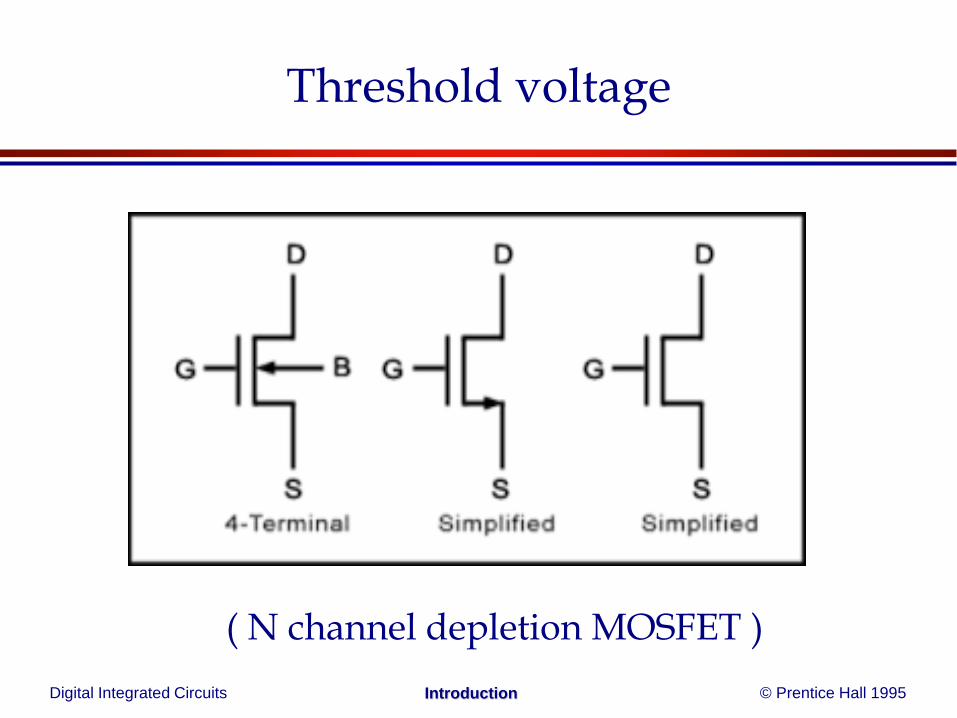
Digital Integrated Circuits © Prentice Hall 1995Introduction
Threshold voltage
( N channel depletion MOSFET )

Digital Integrated Circuits © Prentice Hall 1995Introduction
Operation of MOSFET Transistor
a) Linear region

Digital Integrated Circuits © Prentice Hall 1995Introduction
Operation of MOSFET Transistor
b) Saturation region

Digital Integrated Circuits © Prentice Hall 1995Introduction
Operation of MOSFET Transistor
c) Beyond Saturation region

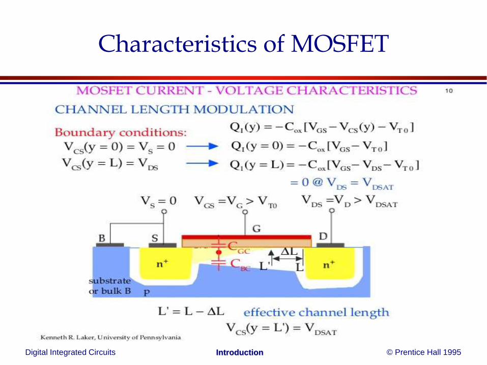
Digital Integrated Circuits © Prentice Hall 1995Introduction
Characteristics of MOSFET
a) Gradual Channel Approximation

Digital Integrated Circuits © Prentice Hall 1995Introduction
Characteristics of MOSFET
a) Gradual Channel Approximation
( V- I characteristics of nMOS Transistor )
Digital Integrated Circuits © Prentice Hall 1995Introduction
Characteristics of MOSFET

Digital Integrated Circuits © Prentice Hall 1995Introduction
Characteristics of MOSFET

Digital Integrated Circuits © Prentice Hall 1995Introduction
Characteristics of MOSFET

Digital Integrated Circuits © Prentice Hall 1995Introduction
Characteristics of MOSFET

Digital Integrated Circuits © Prentice Hall 1995Introduction

Digital Integrated Circuits © Prentice Hall 1995Introduction

Digital Integrated Circuits © Prentice Hall 1995Introduction

Digital Integrated Circuits © Prentice Hall 1995Introduction
Digital Integrated Circuits © Prentice Hall 1995Introduction

Digital Integrated Circuits © Prentice Hall 1995Introduction

Digital Integrated Circuits © Prentice Hall 1995Introduction
Depletion Region
hole diffusionelectron diffusion
p n
hole driftelectron drift
ChargeDensity
Distance
x+
-
Electrical
xField
x
PotentialV
W2-W1
(a) Current flow.
(b) Charge density.
(c) Electric field.
(d) Electrostaticpotential.
Digital Integrated Circuits © Prentice Hall 1995Introduction
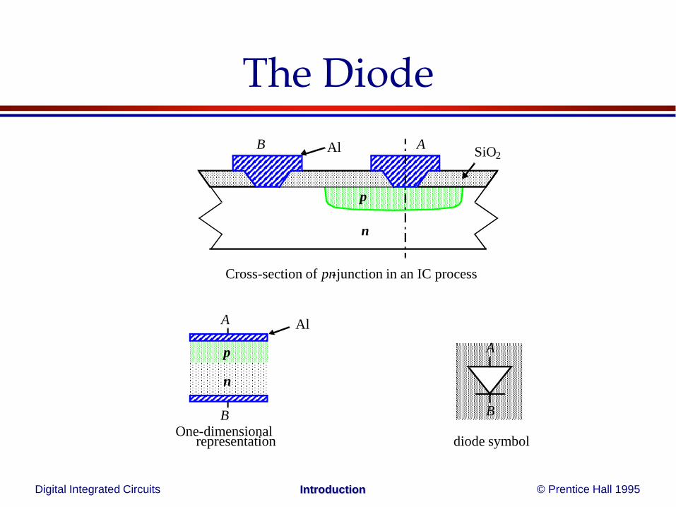
The Diode
n
p
p
n
B ASiO2
Al
A
B
Al
A
B
Cross-section of pn-junction in an IC process
One-dimensionalrepresentation diode symbol

Digital Integrated Circuits © Prentice Hall 1995Introduction
Diode Current

Digital Integrated Circuits © Prentice Hall 1995Introduction
Forward Bias
x
pn0
np0
-W1 W20
pn(W
2)
n-regionp-region
Lp
diffusion
Digital Integrated Circuits © Prentice Hall 1995Introduction
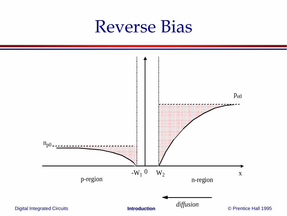
Reverse Bias
x
pn0
np0
-W1 W20
n-regionp-region
diffusion
Digital Integrated Circuits © Prentice Hall 1995Introduction
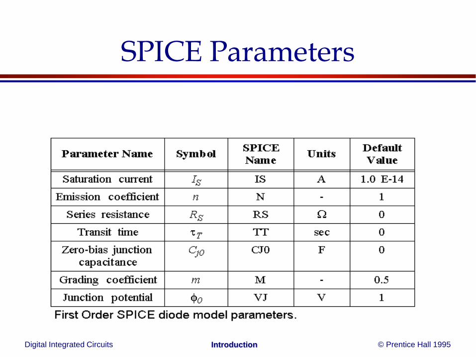
SPICE Parameters

Digital Integrated Circuits © Prentice Hall 1995Introduction
Digital Integrated Circuits © Prentice Hall 1995Introduction
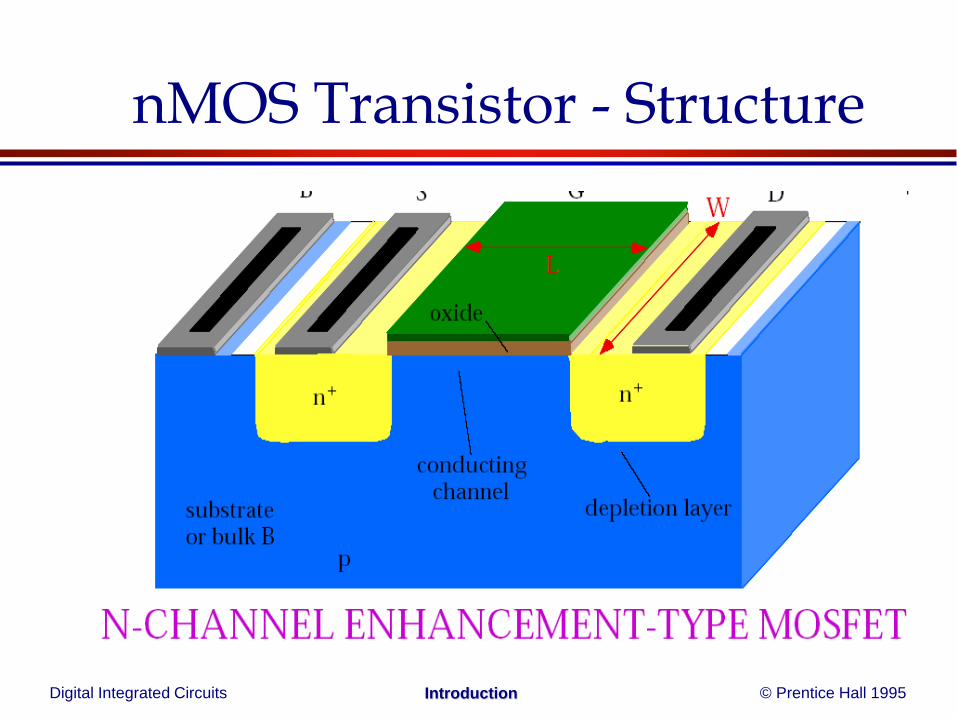
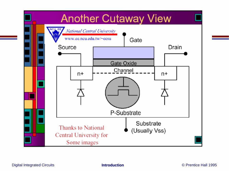
nMOS Transistor - Structure
Digital Integrated Circuits © Prentice Hall 1995Introduction
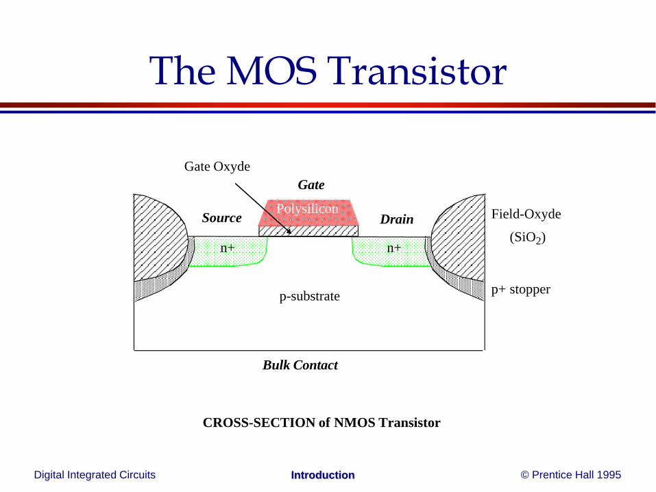
The MOS Transistor
n+n+
p-substrate
Field-Oxyde
(SiO2)
p+ stopper
Polysilicon
Gate Oxyde
DrainSource
Gate
Bulk Contact
CROSS-SECTION of NMOS Transistor

Digital Integrated Circuits © Prentice Hall 1995Introduction
Carriers and Current
Carriers always flow from the Source to Drain
NMOS: Free electrons move from Source to Drain.
Current direction is from Drain to Source.
• PMOS: Free holes move from Source to Drain.
Current direction is from Source to Drain.

Digital Integrated Circuits © Prentice Hall 1995Introduction
IGFET
The dimension of SiO2 layer is about 0.02 to 0.1 micron.
Gate is isolated thus Insulated-Gate FET
Due to insulation the current flowing through the gate terminal is extremely small of the order of 10^-15 A.
Drain is always kept as more positive than the source.
The current flows from the Drain to Source
P-n junctions are kept under the reverse bias conditions
Typically the Length of the device is from 1 to 10 micron.
Digital Integrated Circuits © Prentice Hall 1995Introduction
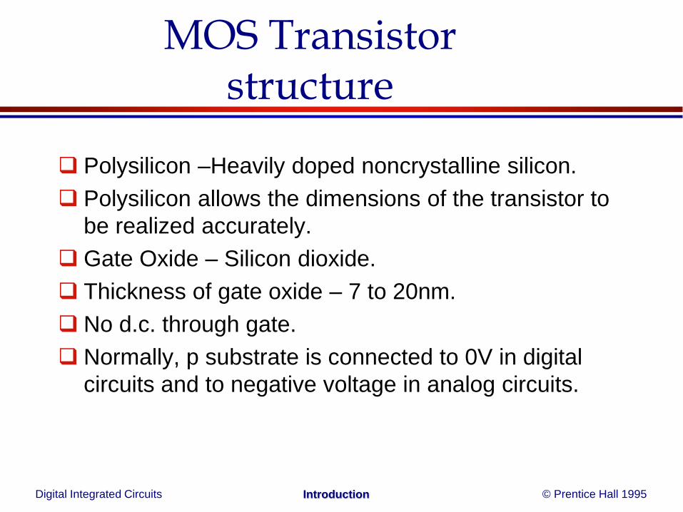
MOS Transistor structure
Polysilicon –Heavily doped noncrystalline silicon.
Polysilicon allows the dimensions of the transistor to
be realized accurately.
Gate Oxide – Silicon dioxide.
Thickness of gate oxide – 7 to 20nm.
No d.c. through gate.
Normally, p substrate is connected to 0V in digital
circuits and to negative voltage in analog circuits.
Digital Integrated Circuits © Prentice Hall 1995Introduction
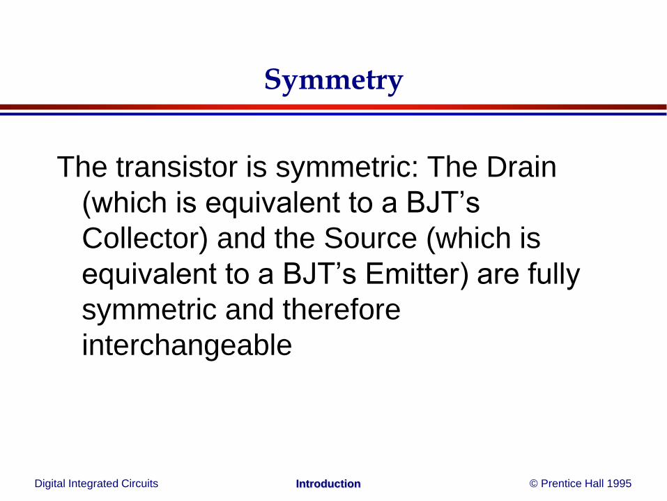
Symmetry
The transistor is symmetric: The Drain
(which is equivalent to a BJT’s
Collector) and the Source (which is
equivalent to a BJT’s Emitter) are fully
symmetric and therefore
interchangeable

Digital Integrated Circuits © Prentice Hall 1995Introduction
All MOS p-n Junctions
Unlike a BJT transistor, in which one of
the p-n junctions is typically forwardly
biased, and the other reversely biased,
in a MOSFET all p-n junctions must
always be kept reversely biased!

Digital Integrated Circuits © Prentice Hall 1995Introduction
The MOSFET Channel
Under certain conditions, a thin channel can
be formed right underneath the Silicon-
Dioxide insulating layer, electrically
connecting the Drain to the Source. The
depth of the channel (and hence its
resistance) can be controlled by the Gate’s
voltage. The length of the channel (shown in
the figures above as L) and the channel’s
width W, are important design parameters.

Digital Integrated Circuits © Prentice Hall 1995Introduction
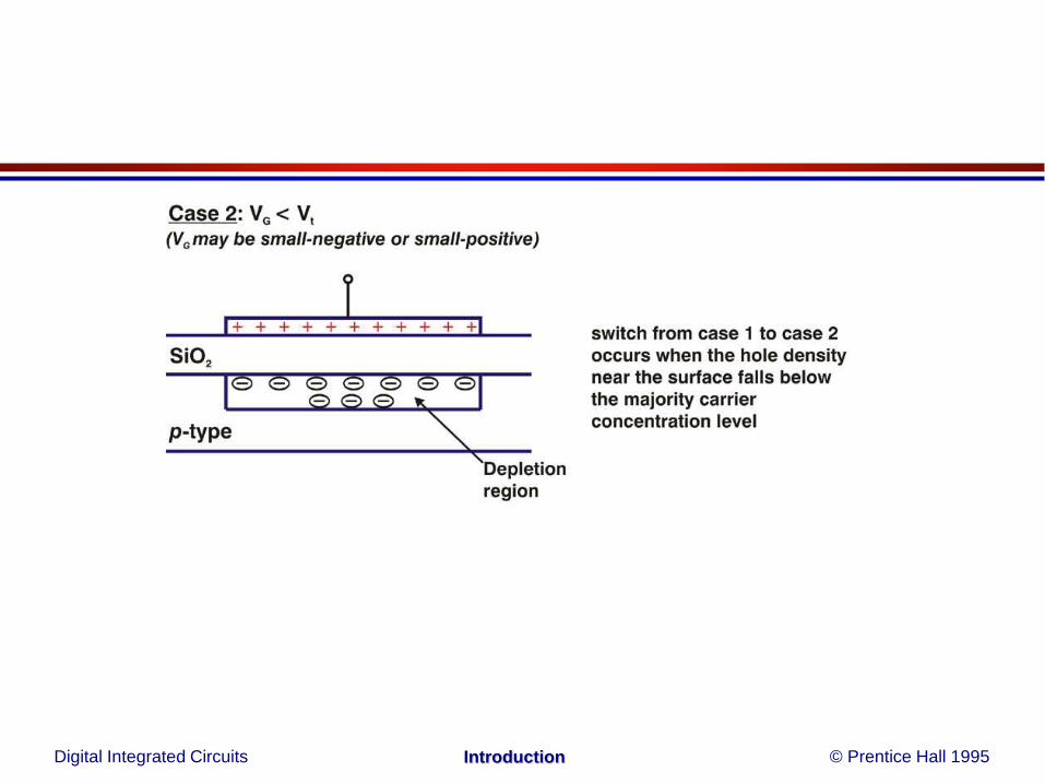
REGION OF OPERATIONCASE-1 (No Gate Voltage)
Two diodes back to back exist in series.
One diode is formed by the pn junction
between the n+ drain region and the p-type
substrate
Second is formed by the pn junction between
the n+ source region and the p-type substrate
These diodes prevent any flow of the current.
There exist a very high resistance.
Digital Integrated Circuits © Prentice Hall 1995Introduction

Digital Integrated Circuits © Prentice Hall 1995Introduction

Digital Integrated Circuits © Prentice Hall 1995Introduction
REGION OF OPERATIONCreating a channel
Apply some positive voltage on the gate terminal.
This positive voltage pushes the holes downward in the substrate region.
This causes the electrons to accumulate under the gate terminal.
At the same time the positive voltage on the gate also attracts the electrons from the n+ region to accumulate under the gate terminal.

Digital Integrated Circuits © Prentice Hall 1995Introduction

Digital Integrated Circuits © Prentice Hall 1995Introduction
Digital Integrated Circuits © Prentice Hall 1995Introduction
Digital Integrated Circuits © Prentice Hall 1995Introduction
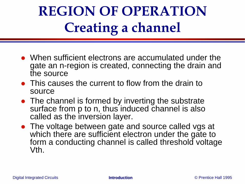
REGION OF OPERATIONCreating a channel
When sufficient electrons are accumulated under the gate an n-region is created, connecting the drain and the source
This causes the current to flow from the drain to source
The channel is formed by inverting the substrate surface from p to n, thus induced channel is also called as the inversion layer.
The voltage between gate and source called vgs at which there are sufficient electron under the gate to form a conducting channel is called threshold voltage Vth.

Digital Integrated Circuits © Prentice Hall 1995Introduction
MOS Channel Formation
Digital Integrated Circuits © Prentice Hall 1995Introduction
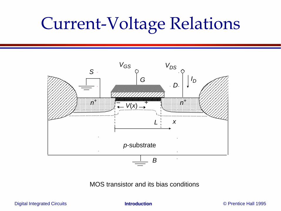
Current-Voltage Relations
n+n+
p-substrate
D
S
G
B
VGS
xL
V(x)+–
VDS
ID
MOS transistor and its bias conditions
Digital Integrated Circuits © Prentice Hall 1995Introduction
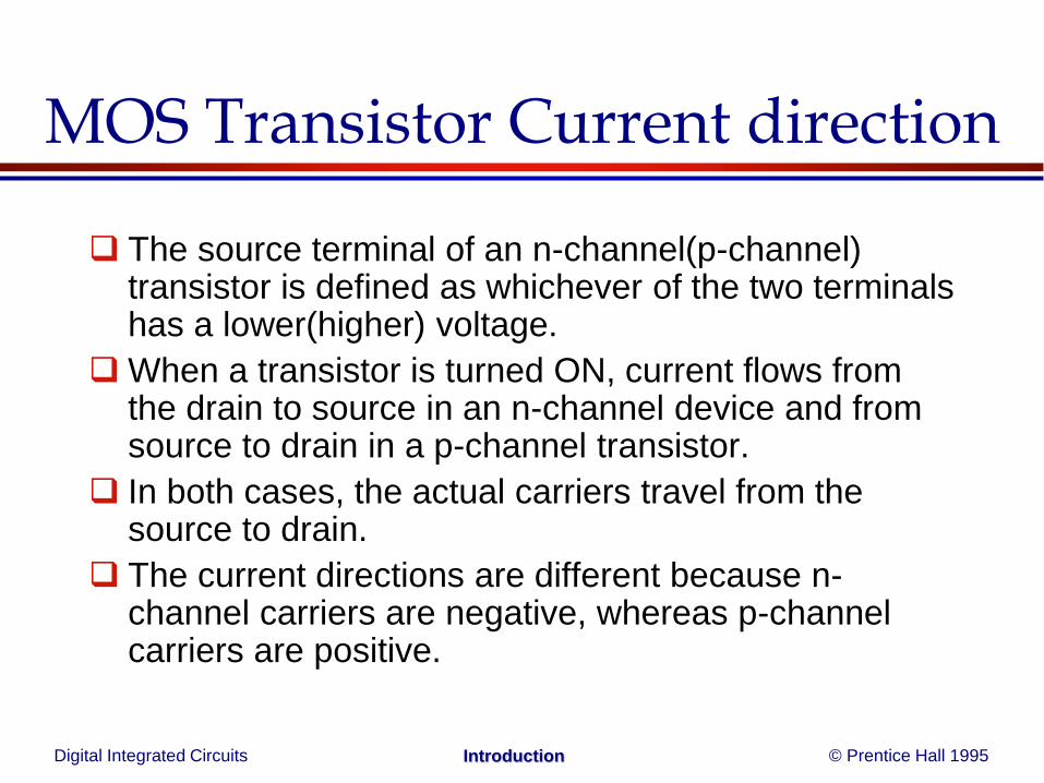
MOS Transistor Current direction
The source terminal of an n-channel(p-channel) transistor is defined as whichever of the two terminals has a lower(higher) voltage.
When a transistor is turned ON, current flows from the drain to source in an n-channel device and from source to drain in a p-channel transistor.
In both cases, the actual carriers travel from the source to drain.
The current directions are different because n-channel carriers are negative, whereas p-channel carriers are positive.
Digital Integrated Circuits © Prentice Hall 1995Introduction
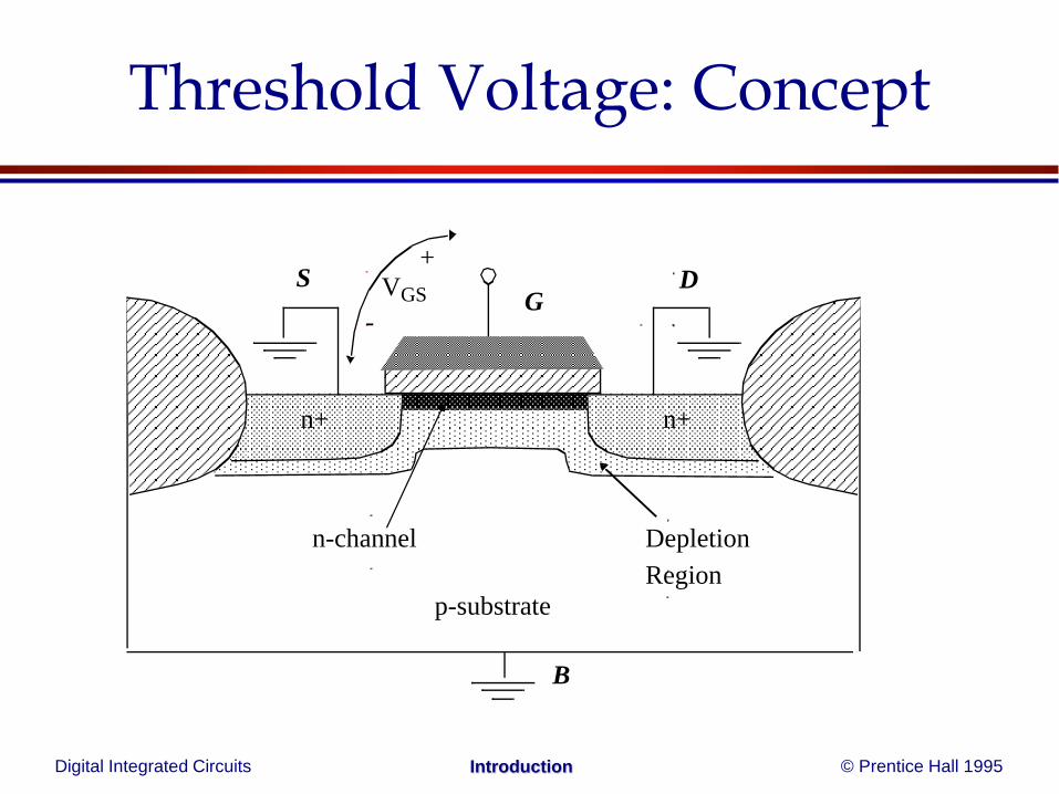
Threshold Voltage: Concept
n+n+
p-substrate
DSG
B
VGS
+
-
Depletion
Region
n-channel
Digital Integrated Circuits © Prentice Hall 1995Introduction
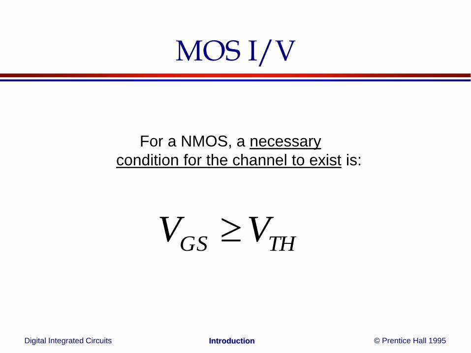
MOS I/V
For a NMOS, a necessary
condition for the channel to exist is:
THGS VV

Digital Integrated Circuits © Prentice Hall 1995Introduction
REGION OF OPERATIONApplying small Vds
Now we applying some small voltage between source and drain say 0.3V.
The voltage Vds causes a current to flow from drain to gate.
Now as we increase the gate voltage, more current will flow.
Increasing the gate voltage above the threshold voltage enhances the channel, hence this mode is called as enhancement mode operation.

Digital Integrated Circuits © Prentice Hall 1995Introduction
MOSFET Current-Voltage Relationships
•The DC gate current is always zero: IG = 0
•Therefore, when a channel is created, the drain
current equals the source current: ID =IS
Digital Integrated Circuits © Prentice Hall 1995Introduction
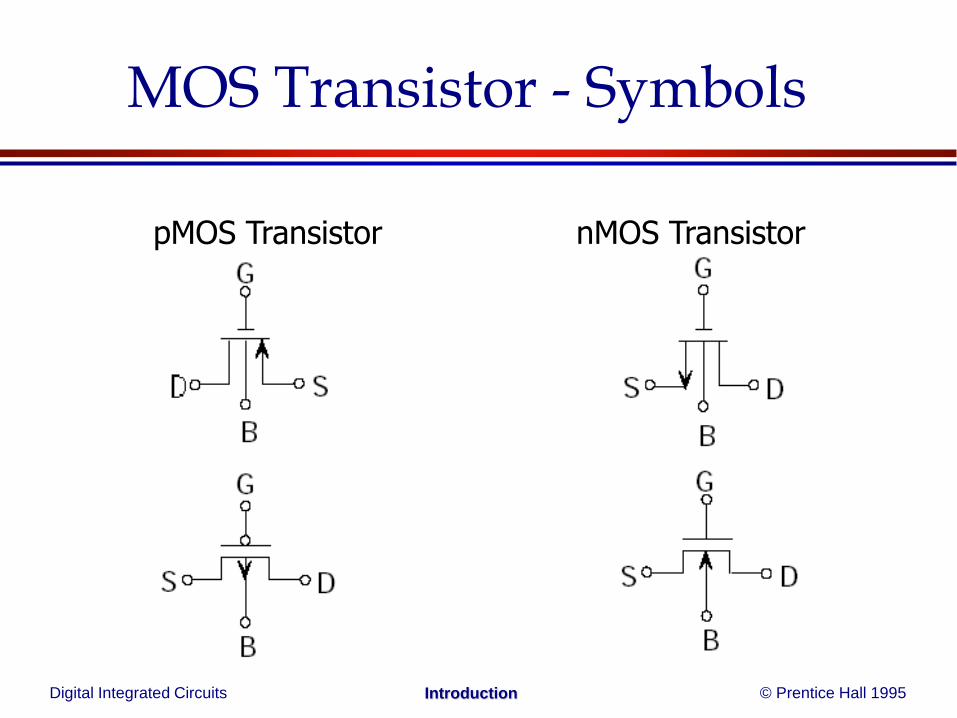
MOS Transistor - Symbols
pMOS Transistor nMOS Transistor
Digital Integrated Circuits © Prentice Hall 1995Introduction
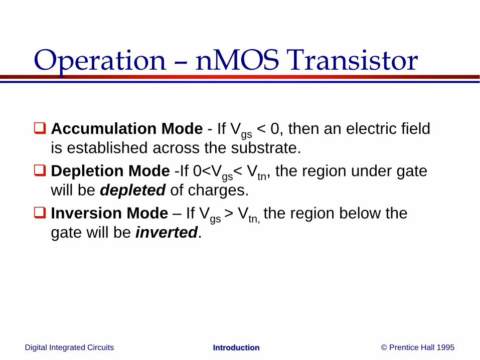
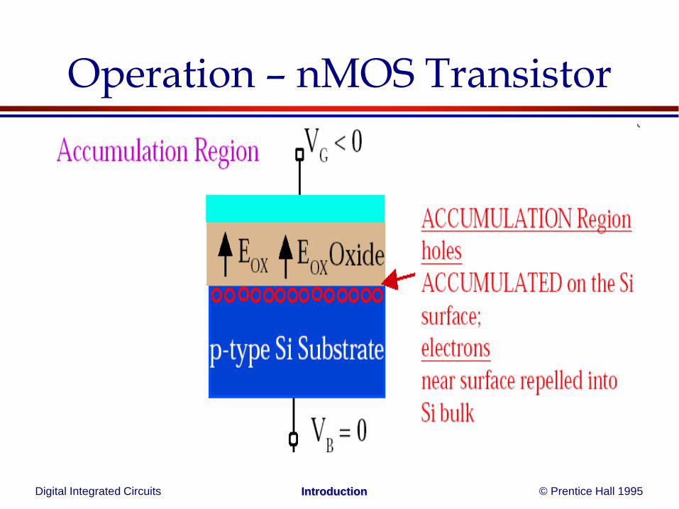
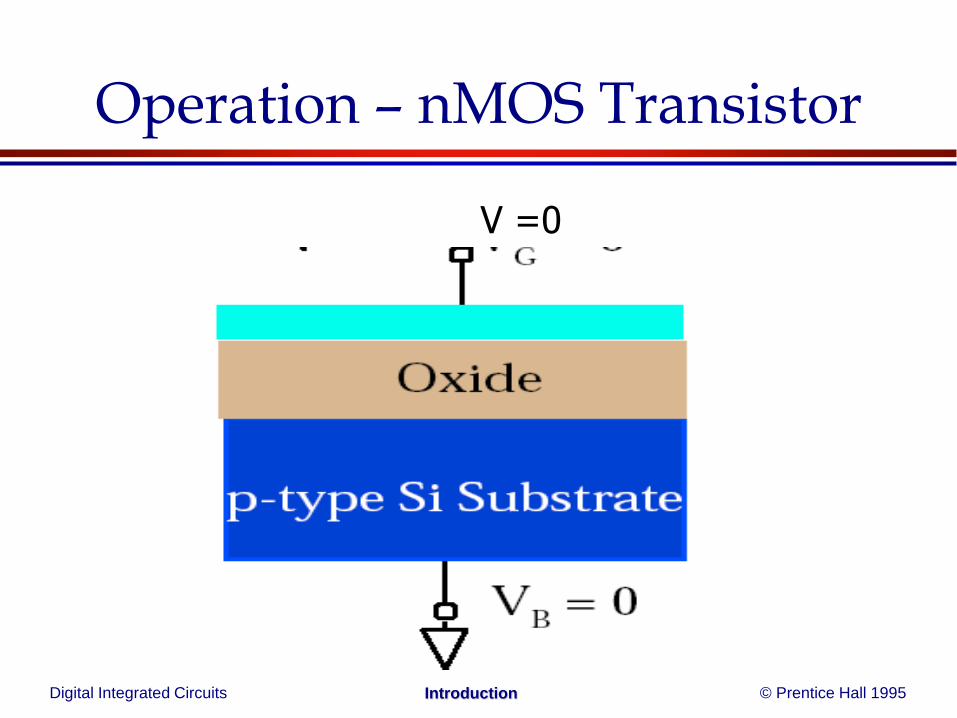
Operation – nMOS Transistor
Accumulation Mode - If Vgs < 0, then an electric field
is established across the substrate.
Depletion Mode -If 0<Vgs< Vtn, the region under gate
will be depleted of charges.
Inversion Mode – If Vgs > Vtn, the region below the
gate will be inverted.
Digital Integrated Circuits © Prentice Hall 1995Introduction
Operation – nMOS Transistor
Digital Integrated Circuits © Prentice Hall 1995Introduction
V =0
Operation – nMOS Transistor

Digital Integrated Circuits © Prentice Hall 1995Introduction
Operation – nMOS Transistor
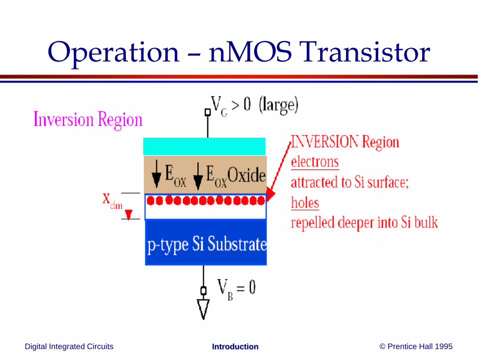
Digital Integrated Circuits © Prentice Hall 1995Introduction
Operation – nMOS Transistor

Digital Integrated Circuits © Prentice Hall 1995Introduction
Operation – nMOS Transistor

Digital Integrated Circuits © Prentice Hall 1995Introduction
Operation – nMOS Transistor
Related Documents