NEC Corporation 1989 Document No. IC-2472B (O. D. No. IC-7208C) Date Published November 1993 P Printed in Japan DATA SHEET MOS INTEGRATED CIRCUIT μPD75P308 The mark ★ shows major revised points. 4-BIT SINGLE-CHIP MICROCOMPUTER DESCRIPTION The μPD75P308 is a model of the μPD75308 equipped with a one-time PROM or EPROM instead of an internal mask ROM. Two types are available as the μPD75P308. The one-time PROM type is ideal for production of a small quantity of many different types of application systems as data can only be written once to the one-time PROM of this type. Programs can be written and rewritten to the built-in EPROM type making it ideal for system evaluation. Detailed functions are described in the followig user's manual. Be sure to read it for designing. μPD75308 User's Manual: IEM-5016 The function common to the one-time PROM and EPROM types of product is referred to as PROM throughout this document. The information in this document is subject to change without notice. FEATURES • μPD75308 compatible • Memory capacity • Program memory (PROM): 8064 x 8 bits • Data memory (RAM): 512 x 4 bits • Can be connected to a pull-up resistor through software: Ports 0-3, 6, 7 • Open-drain input/output: Ports 4 and 5 • Single power source: 5V ± 5% ORDERING INFORMATION Part Number Package Internal ROM μPD75P308GF-3B9 80-pin plastic QFP (14 x 20 mm) One-time PROM μPD75P308K 80-pin ceramic WQFN (LCC w/window) EPROM QUALITY GRADE Part Number Package Quality Grade μPD75P308GF-001-3B9 80-pin plastic QFP (14 x 20 mm) Standard μPD75P308K 80-pin Ceramic WQFN (LCC w/window) Standard ★ Please refer to "Quality Grade on NEC Semiconductor Devices" (Document number IEI-1209) published by NEC Corporation to know the specification of quality grade on the devices and its recommended applications.

Welcome message from author
This document is posted to help you gain knowledge. Please leave a comment to let me know what you think about it! Share it to your friends and learn new things together.
Transcript

NEC Corporation 1989
Document No. IC-2472B(O. D. No. IC-7208C)
Date Published November 1993 PPrinted in Japan
DATA SHEET
MOS INTEGRATED CIRCUIT
µPD75P308
The mark shows major revised points.
4-BIT SINGLE-CHIP MICROCOMPUTER
DESCRIPTION
The µPD75P308 is a model of the µPD75308 equipped with a one-time PROM or EPROM instead of an
internal mask ROM.
Two types are available as the µPD75P308. The one-time PROM type is ideal for production of a small
quantity of many different types of application systems as data can only be written once to the one-time
PROM of this type. Programs can be written and rewritten to the built-in EPROM type making it ideal
for system evaluation.
Detailed functions are described in the followig user's manual. Be sure to read it for designing.
µPD75308 User's Manual: IEM-5016
The function common to the one-time PROM and EPROM types of product is referred to as PROM throughout this document.
The information in this document is subject to change without notice.
FEATURES
• µPD75308 compatible
• Memory capacity
• Program memory (PROM): 8064 x 8 bits
• Data memory (RAM): 512 x 4 bits
• Can be connected to a pull-up resistor through software: Ports 0-3, 6, 7
• Open-drain input/output: Ports 4 and 5
• Single power source: 5V ± 5%
ORDERING INFORMATION
Part Number Package Internal ROM
µPD75P308GF-3B9 80-pin plastic QFP (14 x 20 mm) One-time PROM
µPD75P308K 80-pin ceramic WQFN (LCC w/window) EPROM
QUALITY GRADE
Part Number Package Quality Grade
µPD75P308GF-001-3B9 80-pin plastic QFP (14 x 20 mm) Standard
µPD75P308K 80-pin Ceramic WQFN (LCC w/window) Standard
Please refer to "Quality Grade on NEC Semiconductor Devices" (Document number IEI-1209) published by NECCorporation to know the specification of quality grade on the devices and its recommended applications.
µPD75P308
2
1
2
3
4
5
6
7
8
9
10
11
12
13
14
15
16
17
18
19
20
21
22
23
24
S12
S13
S14
S15
S16
S17
S18
S19
S20
S21
S22
S23
S24/BP0
S25/BP1
S26/BP2
S27/BP3
S28/BP4
S29/BP5
S30/BP6
S31/BP7
COM0
COM1
COM2
COM3
80 79 78 77 76 75 74 73 72 71 70 69 68 67 66 65
S11
S10
S9
S8
S7
S6
S5
S4
S3
S2
S1
S0
RE
SE
T
P73
/KR
7
P72
/KR
6
P71
/KR
5
P70/KR4
P63/KR3
P62/KR2
P61/KR1
P60/KR0
X2
X1
V
XT2
XT1
V
P33 (MD3)
P32 (MD2)
P31/SYNC (MD1)
P30/LCDCL (MD0)
P23/BUS
P22/PCL
P21
P20/PTO0
P13/TI0
P12/INT2
P11/INT1
P10/INT0
P03/SI/SBI
64
63
62
61
60
59
58
57
56
55
54
53
52
51
50
49
48
47
46
45
44
43
42
41
PP
DD
25 26 27 28 29 30 31 32 33 34 35
BIA
S
P40
P41
P42
P43
P50
P51
P52
P53V V VLC
O
LC1
LC2
V
PD
75
P3
08
GF
-3B
9
PD
75
P3
08
K
µµ
SS
P00
/INT4
P01
/SC
K
P02
/SO
/SB
0
36 37 38 39 40
PIN CONFIGURATION

µP
D75P
3083
BLO
CK
D
IAG
RA
M
P00-P03
P10-P13
P20-P23
P30-P33/MD0-MD3
P40-P43
P50-P53
P60-P63
P70-P73
4
4
4
4
4
4
4
4
PORT0
PORT1
PORT2
PORT3
PORT4
PORT5
PORT6
PORT7
S0-S23
S24/BP0-S31/BP7
COM0-COM3
V -V LCO LC2
BIAS
LCDCL/P30
SYNC/P30
24
8
4
3
LCD
CONTROLLER
/DRIVER
fLCD
RESET
SP(8)
BANK
GENERAL REG.
DATAMEMORY
(RAM)512 x 4 BITS
CYALU
VSSVDDVPP
DECODEAND
CONTROL
PROGRAMMEMORY(PROM)
8064 x 8 BITS
PROGRAMCOUNTER(13)
STAND BYCONTROL
SYSTEM CLOCKGENERATORCLOCK
DIVIDER
CLOCKOUTPUT
CONTROL SUB MAIN
f /2X N
X2X1XT2XT1PCL/P22
CPUCLOCK
INTERRUPTCONTROL
BIT SEQ.BUFFER(16)
SERIALINTERFACE
WATCHTIMER
TIMER/EVENTCOUNTER
#0
BASICINTERVALTIMER
TI0/P13
PTO0/P20
BUZ/P23
SI/SBI/P03
SO/SB0/P02
SCK/P01
INTBT
INTT0
INTW
INTCSI
INT0/P10
INT1/P11
INT2/P12
INT4/P00
KR0/P60-KR3/P63,KR4/P70-KR7/P73
8
f LCD
µPD75P308
4
CONTENTS
1. PIN FUNCTIONS ................................................................................................................................. 5
1.1 PORT PINS ................................................................................................................................................. 5
1.2 NON PORT PINS ....................................................................................................................................... 6
1.3 PIN INPUT/OUTPUT CIRCUITS ................................................................................................................ 7
1.4 NOTES ON USING P00/INT4 AND RESET PINS ..................................................................................... 9
2. DIFFERENCES BETWEEN µPD75P308 AND µPD75308 .................................................................. 10
3. WRITING AND VERIFYING PROM (PROGRAM MEMORY) ........................................................... 11
3.1 OPERATION MODES FOR WRITING/VERIFYING PROGRAM MEMORY ............................................ 11
3.2 PROGRAM MEMORY WRITE PROCEDURE .......................................................................................... 12
3.3 PROGRAM MEMORY READ PROCEDURE ............................................................................................ 13
3.4 ERASURE (µPD75P308K ONLY) ............................................................................................................. 14
4. ELECTRICAL SPECIFICATIONS........................................................................................................ 15
5. PACKAGE DRAWINGS ......................................................................................................................28
6. RECOMMENDED SOLDERING CONDITIONS................................................................................. 30
APPENDIX A. DEVELOPMENT TOOLS ................................................................................................. 31
APPENDIX B. RELATED DOCUMENTS ................................................................................................ 32

µPD75P308
5
E-B
P00 Input INT4
P01 Input/Output SCK
P02 Input/Output SO/SB0
P03 Input/Output SI/SBI
P10 INT0
P11 INT1
P12 INT2
P13 TI0
P20 PTO0
P21 —
P22 PCL
P23 BUZ
P30*2
P31*2
P32*2 MD2
P33*2 MD3
P40-43*2 Input/Output —
P50-P53*2 Input/Output —
P60 KR0
P61 KR1
P62 KR2
P63 KR3
P70 KR4
P71 KR5
P72 KR6
P73 KR7
BP0 S24
BP1 S25
BP2 S26
BP3 S27
BP4 S28
BP5 S29
BP6 S30
BP7 S31
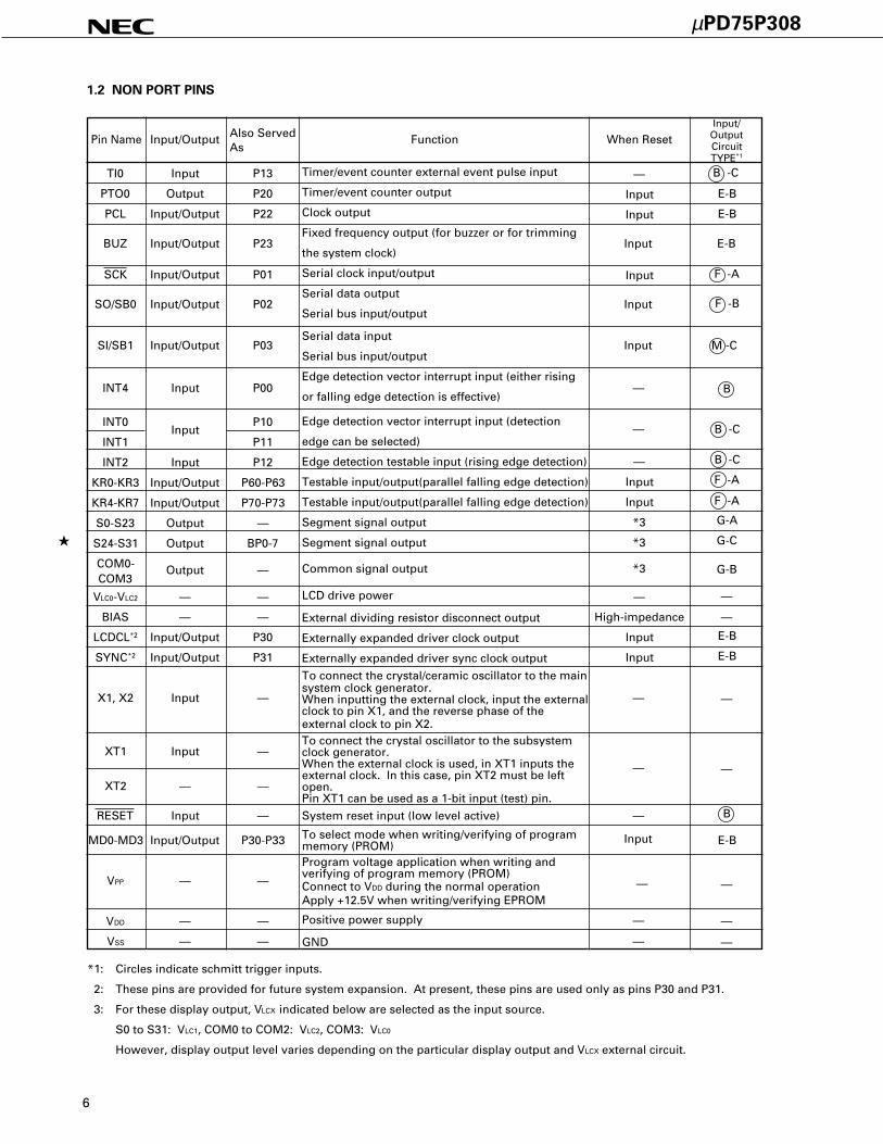
1. PIN FUNCTIONS
1.1 PORT PINS
4-bit input port (PORT0)Pull-up resistors can be specified in 3-bitunits for the P01 to P03 pins by software.
Input
Input/OutputCircuitTYPE*1
Pin Name Input/Output Function 8-Bit I/O When ResetAlso ServedAs
F -A
F -B
B
M -C
Input
X
InputX
4-bit input/output port (PORT2)Internal pull-up resistors can bespecified in 4-bit units by software.
InputX
E-BInputX
MD0LCDCL
SYNC MD1
M-A
M-A
High impedance
High impedance
4-bit input/output port (PORT7)Internal pull-up resistors can bespecified in 4-bit units by software.
Input
Input
1-bit output port (BIT PORT)Shared with a segment output pin. G-C*3X
F -A
F -A
Input/Output
Input/Output
Output
Output
Input/Output
Input/Output
With noise elimination function
4-bit input port (PORT1)Internal pull-up resistors can bespecified in 4-bit units by software.
Programmable 4-bit input/output port(PORT3)This port can be specified for input/outputin bit units.Internal pull-up resistors can bespecified in 4-bit units by software.
N-ch open-drain 4-bit input/output port(PORT4)Data input/output pin for writing andverifying of program memory (PROM)(lower 4 bits)N-ch open-drain 4-bit input/output port(PORT5)Data input/output pin for writing andverifying of program memory (PROM)(upper 4 bits)
Programmable 4-bit input/output port(PORT6)This port can be specified for input/outputin bit units.Internal pull-up resistors can be specifiedin 4-bit units by software.
*1: Circles indicate schmitt trigger inputs.
2: Can directly drive LED.
3: For BP0-7, VLC1 indicated below are selected as the input source.
However, the output level is changed depending on BP0-7 and the VLC1 external circuits.
B -C
µPD75P308
6
Timer/event counter external event pulse input
Timer/event counter output
Clock output
Fixed frequency output (for buzzer or for trimming
the system clock)
Serial clock input/output
Serial data output
Serial bus input/output
Serial data input
Serial bus input/output
Edge detection vector interrupt input (either rising
or falling edge detection is effective)
Edge detection vector interrupt input (detection
edge can be selected)
Edge detection testable input (rising edge detection)
Testable input/output(parallel falling edge detection)
Testable input/output(parallel falling edge detection)
Segment signal output
Segment signal output
Common signal output
LCD drive power
External dividing resistor disconnect output
Externally expanded driver clock output
Externally expanded driver sync clock output
To connect the crystal/ceramic oscillator to the mainsystem clock generator.When inputting the external clock, input the externalclock to pin X1, and the reverse phase of theexternal clock to pin X2.To connect the crystal oscillator to the subsystemclock generator.When the external clock is used, in XT1 inputs theexternal clock. In this case, pin XT2 must be leftopen.Pin XT1 can be used as a 1-bit input (test) pin.
System reset input (low level active)
To select mode when writing/verifying of programmemory (PROM)Program voltage application when writing andverifying of program memory (PROM)Connect to VDD during the normal operationApply +12.5V when writing/verifying EPROM
Positive power supply
GND
—
Input
—
1.2 NON PORT PINS
TI0 Input P13
PTO0 Output P20
PCL Input/Output P22
SCK Input/Output P01
INT0 P10
INT1 P11
INT2 Input P12
KR0-KR3 Input/Output P60-P63
KR4-KR7 Input/Output P70-P73
S0-S23 Output —
S24-S31 Output BP0-7
COM0-COM3
VLC0-VLC2 — —
BIAS — —
LCDCL*2 Input/Output P30
SYNC*2 Input/Output P31
RESET Input —
MD0-MD3 Input/Output P30-P33
VDD — —
VSS — —
Input/OutputCircuitTYPE*1
Pin Name Input/Output Function When Reset
—
Input
Input
Input
—
Input
Input
*3
*3
*3
—
High-impedance
Input
Input
E-B
E-B
BUZ Input/Output P23 Input E-B
F -A
SO/SB0 Input/Output P02 Input F -B
SI/SB1 Input/Output P03 Input M -C
INT4 Input P00 — B
Input B -C
B -C
F -A
F -A
G-A
G-C
G-BOutput —
—
—
E-B
E-B
X1, X2 Input — — —
— —
XT1 Input —
XT2 — —
—
E-B
VPP — — —
— —
— —
*1: Circles indicate schmitt trigger inputs.
2: These pins are provided for future system expansion. At present, these pins are used only as pins P30 and P31.
3: For these display output, VLCX indicated below are selected as the input source.
S0 to S31: VLC1, COM0 to COM2: VLC2, COM3: VLC0
However, display output level varies depending on the particular display output and VLCX external circuit.
B
B -C
Also ServedAs

µPD75P308
7
1.3 PIN INPUT/OUTPUT CIRCUITS
The following shows a simplified input/output circuit diagram for each pin of the µPD75P308.
TYPE A (for TYPE E–B) TYPE D (for TYPE E–B, F-A)
TYPE B TYPE E–B
IN
VDD
P–ch
N–ch
Input buffer of CMOS standard
data
outputdisable
OUT
P–ch
N–ch
Push–pull output that can be set in a outputhigh–impedance state (both P–ch and N–ch are off)
IN
Schmitt trigger input with hysteresis characteristics
data
outputdisable
Type D
Type A
P.U.R.enable
VDD
P.U.R.
P–ch
IN/OUT
P.U.R. : Pull–Up Resistor
P.U.R.enable
VDD
P.U.R.
P–ch
TYPE B–C TYPE E–E
IN
P.U.R. : Pull–Up Resistor
P.U.R. : Pull–Up Resistor
Schmitt trigger input with hysteresis characteristics
data
outputdisable
Type A
P.U.R.enable
VDD
P.U.R.
P–ch
IN/OUT
Type B
Type D
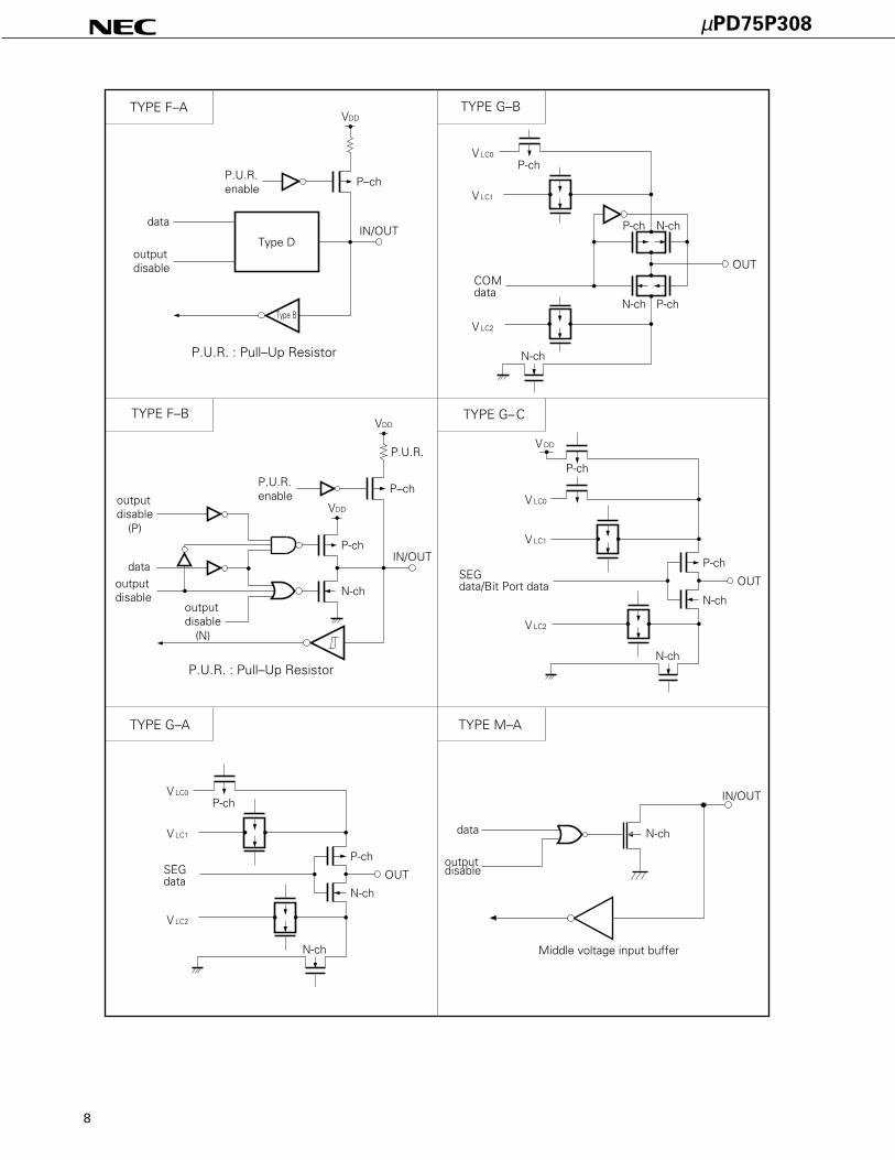
µPD75P308
8
P-ch
TYPE F–A
TYPE G–C
TYPE G–A
TYPE G–B
V DD
V LC0
V LC0
V LC1
V LC2
SEGdata/Bit Port data
P-ch
N-ch
OUT
N-ch
V LC1
V LC2
P-ch
P-ch
N-ch
OUT
N-ch
V LC0
V LC1
V LC2
P-ch
N-ch
SEGdata
COMdata
OUT
P-ch N-ch
N-ch P-ch
data
outputdisable
Type D
Type B
P.U.R.enable
VDD
P–ch
IN/OUT
P.U.R. : Pull–Up Resistor
TYPE F–B
P.U.R. : Pull–Up Resistor
dataoutputdisable
P.U.R.enable
VDD
P.U.R.
P–ch
N-ch
P-ch
outputdisable
(P)
outputdisable
(N)
VDD
IN/OUT
IN/OUT
N-chdata
outputdisable
TYPE M–A
Middle voltage input buffer

µPD75P308
9
TYPE M-C
data
outputdisable
P.U.R.enable
VDD
P.U.R.
IN/OUT
P–ch
N-ch
P.U.R. : Pull–Up Resistor
1.4 NOTES ON USING P00/INT4 AND RESET PINS
In addition to the functions shown in sections 1.1 and 1.2, the P00/INT4 and RESET pins also have a function
to set a test mode (for IC testing) in which the internal operations of the µPD75P308 are tested.
When a voltage higher than VDD is applied to either of these pins, the test mode is set. This means that, even
during ordinary operation, the µPD75P308 may be set in the test mode if a noise exceeding VDD is applied.
For example, if the wiring length of the P00/INT4 or RESET pin is too long, noise superimposed on the wiring
line of the pin may cause the above problem.
Therefore, keep the wiring length of these pins as short as possible to suppress the noise; otherwise, take noise
preventive measures as shown below by using external components.
• Connect diode with low VF between VDD
and P00/INT4, RESET pin
• Connect capacitor between VDD
and P00/INT4, RESET pin
V DD V DD
V DDV DD
P00/INT4, RESET
Diode withlow V F
P00/INT4, RESET

µPD75P308
10
Item µPD75P308K µPD75P308GF µPD75308GF
• EPROM • PROM (one-time model) • Mask ROM
• 0000H-1F7FH • 0000H-1F7FH • 0000H-1F7FH
• 8064 x 8 bits • 8064 x 8 bits • 8064 x 8 bits
Pull-up Resistor Ports 4, 5
Dividing Resistor for LCD
Driving Power Supply
Pins 50-53 P30/MD0-P33/MD3 P30-P33
Pin 57 VPP NC
Current dissipations and operating temperature ranges differ between µPD75P308 and
µPD75308. For detail, refer to the specification documents of each mode.
Operating Voltage Range 5V±5% 2.7-6.0V
80-pin ceramic WQFN
(LCC w/window)
Noise immunity and noise radiation differ because circuit scale and mask layout are
different.
2. DIFFERENCES BETWEEN µPD75P308 AND µPD75308
The µPD75P308 is a model of the µPD75308 and is equipped with a PROM instead of a mask ROM.
Programs can be rewritten to the PROM of the µPD75P308. Table 2-1 shows the differences between the
µPD75P308 and µPD75308. You should fully consider these differences when you debug or produce your
application system on an experimental basis by using the PROM model, and then proceed to mass-produce
the system by using the mask ROM model.
For the details of the CPU and the internal hardware, refer to µPD75308 User's Manual (IEM-5016).
Table 2-1 Differences between µPD75P308 and µPD75308
Program Memory
Note: The noise immunity and noise radiation differ between the PROM and mask ROM models. To replace
the PROM model with the mask ROM model in the course of experimental production to mass
production, evaluate your system by using the CS mode (not ES model) of the mask ROM model.
Pin Connection
Not provided Mask option
Not provided Mask option
Electrical Specifications
Package
Others
80-pin plastic QFP (14 x 20 mm)
µPD75P308
11
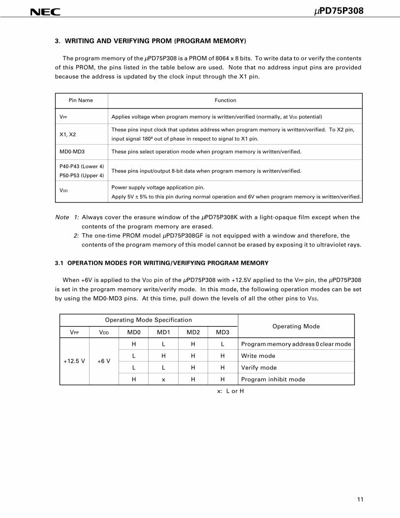
Pin Name Function
VPP Applies voltage when program memory is written/verified (normally, at VDD potential)
These pins input clock that updates address when program memory is written/verified. To X2 pin,
input signal 180º out of phase in respect to signal to X1 pin.
MD0-MD3 These pins select operation mode when program memory is written/verified.
P40-P43 (Lower 4)
P50-P53 (Upper 4)
Power supply voltage application pin.
Apply 5V ± 5% to this pin during normal operation and 6V when program memory is written/verified.
3. WRITING AND VERIFYING PROM (PROGRAM MEMORY)
The program memory of the µPD75P308 is a PROM of 8064 x 8 bits. To write data to or verify the contents
of this PROM, the pins listed in the table below are used. Note that no address input pins are provided
because the address is updated by the clock input through the X1 pin.
These pins input/output 8-bit data when program memory is written/verified.
VDD
X1, X2
Note 1: Always cover the erasure window of the µPD75P308K with a light-opaque film except when the
contents of the program memory are erased.
2: The one-time PROM model µPD75P308GF is not equipped with a window and therefore, the
contents of the program memory of this model cannot be erased by exposing it to ultraviolet rays.
3.1 OPERATION MODES FOR WRITING/VERIFYING PROGRAM MEMORY
When +6V is applied to the VDD pin of the µPD75P308 with +12.5V applied to the VPP pin, the µPD75P308
is set in the program memory write/verify mode. In this mode, the following operation modes can be set
by using the MD0-MD3 pins. At this time, pull down the levels of all the other pins to VSS.
Operating Mode Specification
MD0 MD1 MD2 MD3
H L H L
L H H H
L L H H
H x H H
VDD
+6 V
VPP
+12.5 V
Operating Mode
Program memory address 0 clear mode
Write mode
Verify mode
Program inhibit mode
x: L or H
µPD75P308
12
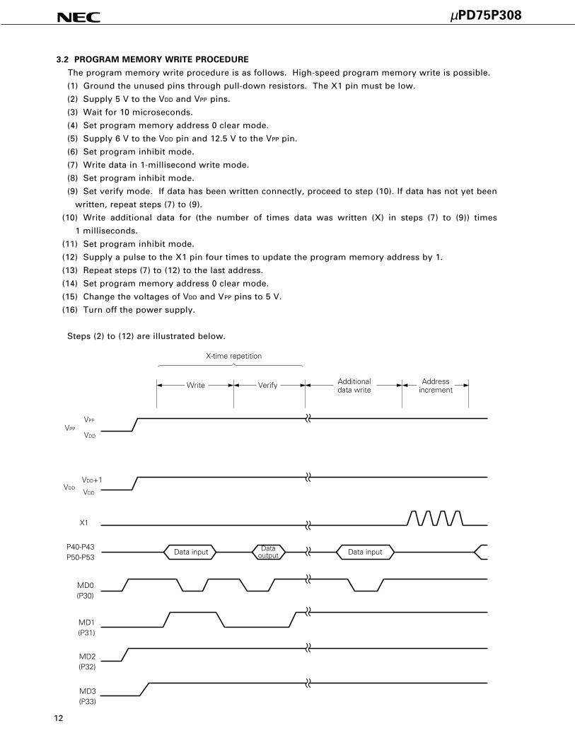
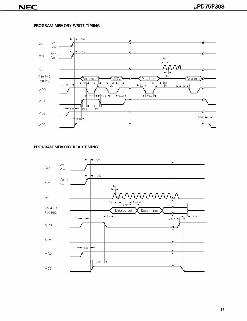
3.2 PROGRAM MEMORY WRITE PROCEDURE
The program memory write procedure is as follows. High-speed program memory write is possible.
(1) Ground the unused pins through pull-down resistors. The X1 pin must be low.
(2) Supply 5 V to the VDD and VPP pins.
(3) Wait for 10 microseconds.
(4) Set program memory address 0 clear mode.
(5) Supply 6 V to the VDD pin and 12.5 V to the VPP pin.
(6) Set program inhibit mode.
(7) Write data in 1-millisecond write mode.
(8) Set program inhibit mode.
(9) Set verify mode. If data has been written connectly, proceed to step (10). If data has not yet been
written, repeat steps (7) to (9).
(10) Write additional data for (the number of times data was written (X) in steps (7) to (9)) times
1 milliseconds.
(11) Set program inhibit mode.
(12) Supply a pulse to the X1 pin four times to update the program memory address by 1.
(13) Repeat steps (7) to (12) to the last address.
(14) Set program memory address 0 clear mode.
(15) Change the voltages of VDD and VPP pins to 5 V.
(16) Turn off the power supply.
Steps (2) to (12) are illustrated below.
VPP
VDD
VDD+1
VDD
VPP
VDD
Data input Dataoutput Data input
Write Verify Additionaldata write
Addressincrement
X-time repetition
P40-P43P50-P53
MD0(P30)
MD1(P31)
MD2(P32)
MD3(P33)
X1

µPD75P308
13
3.3 PROGRAM MEMORY READ PROCEDURE
The contents of the program memory can be read in the following procedure.
(1) Ground the unused pins through pull-down resistors. The X1 pin must be low.
(2) Supply 5 V to the VDD and VPP pins.
(3) Wait for 10 microseconds.
(4) Set program memory address 0 clear mode.
(5) Supply 6 V to the VDD pin and 12.5 V to the VPP pin.
(6) Set program inhibit mode.
(7) Set verify mode. Data of each address is sequentially output each time a clock pulse is input to the
X1 pin four times.
(8) Set program inhibit mode.
(9) Set program memory address 0 clear mode.
(10) Change the voltages of VDD and VPP pins to 5 V.
(11) Turn off the power supply.
Steps (2) to (9) are illustrated below.
VPP
VDD
VDD+1
VDD
VPP
VDD
Data output Data outputP40-P43P50-P53
MD0(P30)
MD1(P31)
MD2(P32)
MD3(P33)
X1

µPD75P308
14
3.4 ERASURE (µPD75P308K ONLY)
The contents of the data programmed to the µPD75P308 can be erased by exposing the window of the
program memory to ultraviolet rays.
The wavelength of the ultraviolet rays used to erase the contents is about 250 nm, and the quantity of the
ultraviolet rays necessary for complete erasure is 15 W.s/cm2 (= ultraviolet ray intensity x erasure time).
When a commercially available ultraviolet ray lamp (wavelength: 254 nm, intensity: 12 mW/cm2) is used,
about 15 to 20 minutes is required.
Note 1: The contents of the program memory may be erased when the µPD75P308 is exposed for a long
time to direct sunlight or the light of fluorescent lamps. To protect the contents from being
erased, mask the window of the program memory with the light-opaque film supplied as an
accessory with the UV EPROM products.
2: To erase the memory contents, the distance between the ultraviolet ray lamp and the µPD75P308
should be 2.5 cm or less.
Remarks: The time required for erasure changes depending on the degradation of the ultraviolet ray
lamp and the surface condition (dirt) of the window of the program memory.
µPD75P308
15
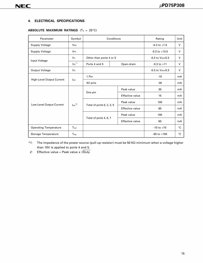
4. ELECTRICAL SPECIFICATIONS
ABSOLUTE MAXIMUM RATINGS (Ta = 25°C)
Parameter Symbol Conditions Rating Unit
Supply Voltage VDD -0.3 to +7.0 V
Supply Voltage VPP -0.3 to +13.5 V
VI1 Other than ports 4 or 5 -0.3 to VDD+0.3 V
VI2*1 Ports 4 and 5 Open-drain -0.3 to +11 V
Output Voltage VO -0.3 to VDD+0.3 V
1 Pin -15 mAIOH
All pins -30 mA
Peak value 30 mA
Effective value 15 mA
Peak value 100 mA
Effective value 60 mA
Peak value 100 mA
Effective value 60 mA
Operating Temperature Topt -10 to +70 °C
Storage Temperature Tstg -65 to +150 °C
*1: The impedance of the power source (pull-up resistor) must be 50 KΩ minimum when a voltage higher
than 10V is applied to ports 4 and 5.
2: Effective value = Peak value x √Duty
One pin
Total of ports 0, 2, 3, 5
Total of ports 4, 6, 7
IOH*2
High-Level Output Current
Low-Level Output Current
Input Voltage

µPD75P308
16
Ceramic*3 Oscillation
frequency (fXX)*1
Oscillation stabilization After VDD came to MIN.
time*2 of oscillation voltage range
Crystal Oscilaltion
frequency (fXX)*1
Oscillation stabilization
time*2
External Clock X1 input frequency
(fX)*1
X1 input high-, low-level
widths (tXH, tXL)
MAIN SYSTEM CLOCK OSCILLATOR CIRCUIT CHARACTERISTICS
(Ta = -10 to +70°C, VDD = 5 to ±5 V)
Oscillator Item Conditions MIN. TYP. MAX. Unit
X1 X2
C1 C2
VDD
X1 X2
C1 C2
VDD
X1 X2
PD74HCU04µ
1.0 5.0*4 MHz
4 ms
1.0 4.19 5.0*4 MHz
10 ms
1.0 5.0*4 MHz
100 500 ns
Recommended
Constants
* 1: The oscillation frequency and X1 input frequency are indicated only to express the characteristics of the
oscillator circuit.
For instruction execution time, refer to AC Characteristics.
2: Time required for oscillation to stabilize after VDD reaches the minimum value of the oscillation voltage
range or the STOP mode has been released.
3: The oscillators below are recommended.
4: When the oscillation frequency is 4.19 MHz < fx ≤ 5.0 MHz, do not select PCC = 0011 as the instruction
execution time: otherwise, one machine cycle is set to less than 0.95 µs, falling short of the rated
minimum value of 0.95 µs.
Caution: When using the oscillation circuit of the main system clock, wire the portion enclosed in dotted
line in the figures as follows to avoid adverse influences on the wiring capacity:
• Keep the wiring length as short as possible.
• Do not cross the wiring over the other signal lines. Do not route the wiring in the vicinity of
lines through which a high alternating current flows.
• Always keep the ground point of the capacitor of the oscillator circuit at the same potential
as VDD. Do not connect the power source pattern through which a high current flows.
• Do not extract signals from the oscillation circuit.
CSA 2.00MG 30 30 4.75 5.25
CSA 4.19MG 30 30 4.75 5.25
CSA 4.19MGU 30 30 4.75 5.25
CST 4.19MG 30 pF (internal) 30 pF (internal) 4.75 5.25
C1
MurataMfg.Co., Ltd.
Manufac-turer
MAX.MIN.
OscillationVoltage Range [V]
C2
External Capacitance [pF]Product Name
RECOMMENDED OSCILLATION CIRCUIT CONSTANTS
MAIN SYSTEM CLOCK: CERAMIC OSCILLATOR (Ta = -10 to +70°C)
µPD75P308
17
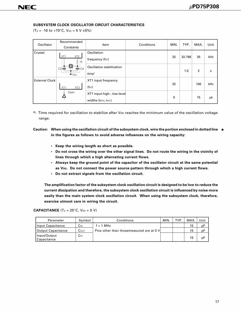
32 32.768 35 kHz
1.0 2 s
32 100 kHz
5 15 µs
Crystal Oscillation
frequency (fXT)
Oscillation stabilization
time*
External Clock XT1 input frequency
(fXT)
XT1 input high-, low-level
widths (tXTH, tXTL)
SUBSYSTEM CLOCK OSCILLATOR CIRCUIT CHARACTERISTICS
(Ta = -10 to +70°C, VDD = 5 V ±5%)
Oscillator Item Conditions MIN. TYP. MAX. UnitRecommended
Constants
XT1 XT2
R
C3 C4
VDD
XT1 XT2
Open
*: Time required for oscillation to stabilize after VDD reaches the minimum value of the oscillation voltage
range.
Caution: When using the oscillation circuit of the subsystem clock, wire the portion enclosed in dotted line
in the figures as follows to avoid adverse influences on the wiring capacity:
• Keep the wiring length as short as possible.
• Do not cross the wiring over the other signal lines. Do not route the wiring in the vicinity of
lines through which a high alternating current flows.
• Always keep the ground point of the capacitor of the oscillator circuit at the same potential
as VDD. Do not connect the power source pattern through which a high current flows.
• Do not extract signals from the oscillation circuit.
The amplification factor of the subsystem clock oscillation circuit is designed to be low to reduce the
current dissipation and therefore, the subsystem clock oscillation circuit is influenced by noise more
easily than the main system clock oscillation circuit. When using the subsystem clock, therefore,
exercise utmost care in wiring the circuit.
CAPACITANCE (Ta = 25°C, VDD = 0 V)
Parameter Symbol Conditions MIN. TYP. MAX. Unit
Input Capacitance CIN f = 1 MHz 15 pF
Output Capacitance COUT Pins other than thosemeasured are at 0 V 15 pF
Input/Output CIO15 pFCapacitance

µPD75P308
18
Ports 2, 3
Ports 0, 1, 6, 7, RESET
Ports 4, 5 Open-drain
X1, X2, XT1
Ports 2, 3, 4, 5
Ports 0, 1, 6, 7, RESET
X1, X2, XT1Ports 0, 2, 3, IOH = -1mA6, 7BIAS
BP0-7 IOH = -100µA*1
Ports 0, 2, 3, Ports 3, 4, 5
6, 7 IOL = 15mA
IOL = 1.6mASB0, 1Open-drain
BP0-7 IOL = 100µA*1
Other than below
X1, X2, XT1
VIN = 10V Ports 4, 5
Other than below
X1, X2, XT1
VOUT = VDD Other than below
VOUT = 10V Ports 4.5
VOUT = 0V
Ports 0, 1, 2, 3, 6, 7(except P00) VIN = 0V
VLCD0 = VLCD
VLCD1 = VLCD x —
VLCD2 = VLCD x —
2.7 V ≤ VLCD ≤ VDD
*6
HALT mode
HALT mode
VIH1
VIH2
VIH3
VIH4
VIL1
VIL2
VIL3
VOH2
VOL1
VOL3
ILIH1
ILIH2
ILIH3
ILIL1
ILIL2
ILOH1
ILOH2
ILOL
VLCD
IDD1
IDD2
High-Level Input Voltage
Low-Level Input Voltage
High-Level Output Voltage
Low-Level Output Voltage
High-Level Input Leakage Current
Low-Level Input Leakage Current
High-Level Output Leakage Current
Low-Level Output Leakage Current
Internal Pull-Up Resistor
LCD Drive Voltage
LCD Output Voltage Deviation
(Common)
LCD Output Voltage Deviation
(Segment)
Supply Current
0.7 VDD VDD V
0.8 VDD VDD V
0.7 VDD 10 V
VDD-0.5 VDD V
0 0.3 VDD V
0 0.2 VDD V
0 0.4 V
VDD-1.0
VDD-2.0 V
0.4 V
1.0 V
3 µA
20 µA
20 µA
-3 µA
-20 µA
3 µA
20 µA
-3 µA
2.5 VDD V
5 15 mA
500 1500 µA
350 1000
35 100
DC CHARACTERISTICS (Ta = -10 to +70°C, VDD = 5V ±5%)
Parameter Symbol Conditions MIN. TYP. MAX. Unit
0.4 2.0 V
0.2VDD VPull-up R ≥ 1kΩ
VIN = VDD
VIN = 0V
VODC
VODS
I0 = ±5 µA 0 ±0.2V V
I0 = ±1 µA 0 ±0.2V V
2
313
µA
15 40 80 KΩ
0.5 20 µAXT1 = 0V
STOP mode
4.19MHz crystal *4
oscillatorC1 = C2 = 22pF
32 kHz *5
crystal oscillator
*3
*2
*2
* 1: When using two of BP0-BP3 and two of BP4-BP7 for output at the same time.
2: "Voltage deviation" means the difference between the ideal segment or common output value
(VLCDn: = 0, 1, 2) and output voltage.
3: Currents for the built-in pull-up resistor are not included.
4: Including when the subsystem clock is operated.
5: When operated with the subsystem clock by setting the system clock control register (SCC) to
1001 to stop the main system clock operation.
6: When operand in the high-speed mode with the processor clock control register (PCC) set to 0011.
VOH1 V
VOL2
RLI
IDD3
IDD4
µPD75P308
19
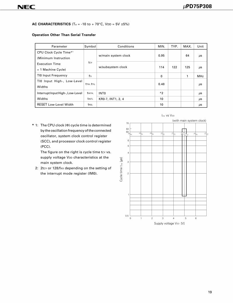
AC CHARACTERISTICS (Ta = -10 to + 70°C, VDD = 5V ±5%)
Operation Other Than Serial Transfer
Parameter Symbol Conditions MIN. TYP. MAX. Unit
w/main system clock
w/subsystem clock
INT0
KR0-7, INT1, 2, 4
tCY
fTI
tTIH, tTIL
tINTH,
tINTL
tRSL
CPU Clock Cycle Time*1
(Minimum Instruction
Execution Time
= 1 Machine Cycle)
TI0 Input Frequency
TI0 Input High-, Low-Level
Widths
Interrupt Input High-, Low-Level
Widths
RESET Low-Level Width
0.95 64 µs
114 122 125 µs
0 1 MHz
0.48 µs
*2 µs
10 µs
10 µs
0 1 2 3 4 5 60.5
1
2
3
4
5
6
6064
70(with main system clock)
Cyc
le t
ime
t
[ s]
cy
µ
Supply voltage V [V]DD
t vs V cy DD
* 1: The CPU clock (Φ) cycle time is determined
by the oscillation frequency of the connected
oscillator, system clock control register
(SCC), and processor clock control register
(PCC).
The figure on the right is cycle time tCY vs.
supply voltage VDD characteristics at the
main system clock.
2: 2tCY or 128/fXX depending on the setting of
the interrupt mode register (IM0).
µPD75P308
20
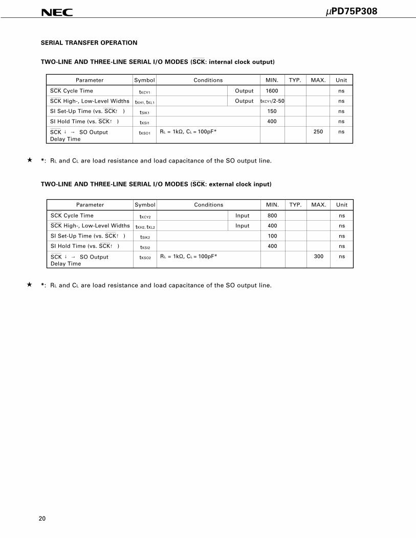
SERIAL TRANSFER OPERATION
TWO-LINE AND THREE-LINE SERIAL I/O MODES (SCK: internal clock output)
Parameter Symbol Conditions MIN. TYP. MAX. Unit
1600 ns
tKCY1/2-50 ns
150 ns
400 ns
250 ns
Output
Output
RL = 1kΩ, CL = 100pF*
tKCY1
tKH1, tKL1
tSIK1
tKSI1
tKSO1
SCK Cycle Time
SCK High-, Low-Level Widths
SI Set-Up Time (vs. SCK )
SI Hold Time (vs. SCK )
SCK SO OutputDelay Time
↑
↑
↓ →
*: RL and CL are load resistance and load capacitance of the SO output line.
TWO-LINE AND THREE-LINE SERIAL I/O MODES (SCK: external clock input)
*: RL and CL are load resistance and load capacitance of the SO output line.
Parameter Symbol Conditions MIN. TYP. MAX. Unit
800 ns
400 ns
100 ns
400 ns
300 ns
Input
Input
RL = 1kΩ, CL = 100pF*
tKCY2
tKH2, tKL2
tSIK2
tKSI2
tKSO2
↑
↓ →
↑
SCK Cycle Time
SCK High-, Low-Level Widths
SI Set-Up Time (vs. SCK )
SI Hold Time (vs. SCK )
SCK SO OutputDelay Time

µPD75P308
21
1600 ns
tKCY/2-50
150 ns
tKCY/2 ns
0 250 ns
tKCY ns
tKCY ns
tKCY ns
tKCY ns
SCK Cycle Time
SCK High-, Low-LevelWidths
SB0, 1 Set-Up Time (vs. SCK )
SB0, 1 Hold Time (vs. SCK )
SCK SB0, 1 OutputDelay Time
SCK SB0, 1
SB0, 1 SCK
SB0, 1 Low-Level Width
SB0, 1 High-Level Width
SBI MODE (SCK: internal clock output (master))
Parameter Symbol Conditions MIN. TYP. MAX. Unit
tKCY3
tKL3
tKH3
tSIK3
tKSI3
tKSO3
tKSB
tSBK
tSBL
tSBH
*: RL and CL are load resistance and load capacitance of the SO output line.
SBI MODE (SCK: external clock output (master))
*: RL and CL are load resistance and load capacitance of the SO output line.
↑
↑
RL = 1kΩ, CL = 100pF* ↓ →
↑ → ↓
↓ → ↓
SCK Cycle Time
SCK High-, Low-LevelWidths
SB0, 1 Set-Up Time (vs. SCK )
SB0, 1 Hold Time (vs. SCK )
SCK SB0, 1 OutputDelay Time
SCK SB0, 1
SB0, 1 SCK
SB0, 1 Low-Level Width
SB0, 1 High-Level Width
Parameter Symbol Conditions MIN. TYP. MAX. Unit
1600 ns
100 ns
tKCY/2 ns
0 300 ns
tKCY ns
tKCY ns
tKCY ns
tKCY ns
tKCY4
tKL4
tKH4
tSIK4
tKSI4
tKSO4
tKSB
tSBK
tSBL
tSBH
↑
↑
RL = 1kΩ, CL = 100pF* ↓ →
↑ → ↓
↓ → ↓
ns
400 ns

µPD75P308
22
AC TIMING TEST POINT (excluding X1 and XT1 inputs)
Test points0.8 VDD
0.2 VDD
0.8 VDD
0.2 VDD
CLOCK TIMING
X1 input VDD –0.5V
0.4 V
tXL tXH
1/fX
XT1 input VDD –0.5V
0.4 V
tXTL tXTH
1/fXT
TI0
tTIL tTIH
1/fTI
TI0 TIMING

µPD75P308
23
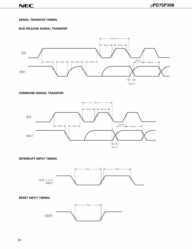
SERIAL TRANSFER TIMING
THREE-LINE SERIAL I/O MODE:
SCK
tKL1 tKH1
tKCY1
Output data
tSIK1 tKSI1
tKSO1
Input dataSI
SO
TWO-LINE SERIAL I/O MODE:
SCK
tKL tKH
tKCY
tSIK tKSI
SB0,1
tKSO
µPD75P308
24
SERIAL TRANSFER TIMING
BUS RELEASE SIGNAL TRANSFER
RESET INPUT TIMING
INT0, 1, 2, 4KR0-7
tINTL tINTH
INTERRUPT INPUT TIMING
SCK
tKL3,4
tKCY3,4
tSIK3,4tKSI3,4
tKSO3,4
SB0,1
tKH3,4
tSBKtKSB
COMMAND SIGNAL TRANSFER
RESET
tRSL
SCK
tKL3,4
tKCY3,4
tSIK3,4tKSI3,4
tKSO3,4
SB0,1
tKH3,4
tSBKtSBHtSBLtKSB

µPD75P308
25
Released by RESET
Released by interrupt
LOW-VOLTAGE DATA RETENTION CHARACTERISTICS OF DATA MEMORY IN STOP MODE
(Ta = -10 to +70°C)
0 µs
217/fX ms
*3 ms
Parameter Symbol Conditions MIN. TYP. MAX. Unit
tSREL
Data Retention Supply
Voltage
Data Retention Supply
Current*1
Release Signal Set Time
Oscillation Stabilization
Wait Time*2
2.0 6.0 V
*1: Does not include current folowing through internal pull-up resistor
2: The oscillation stabilization wait time is the time during which the CPU is stopped to prevent unstable
operation when oscillation is started.
3: Depends on the setting of the basic interval timer mode register (BTM) as follows:
BTM3 BTM2 BTM1 BTM0 WAIT time ( ): fX = 4.19 MHz
— 0 0 — 220/fX (approx. 250 ms)
— 0 1 — 217/fX (approx. 31.3 ms)
— 1 0 — 215/fX (approx. 7.82 ms)
— 1 1 — 213/fX (approx. 1.95 ms)
DATA RETENTION TIMING (releasing STOP mode by RESET)
DATA RETENTION TIMING (standby release signal: releasing STOP mode by interrupt)
STOP mode
Data retention mode
STOP instruction execution
VDD
VDDDRtSREL
tWAIT
Operationmode
HALT mode
Standby release signal(interrupt request)
IDDDR VDDDR = 2.0V 0.1 10 µA
STOP mode
Data retention mode
STOP instructionexecution
VDD
RESET
VDDDRtSREL
tWAIT
Operationmode
Internal reset operation
HALT mode
VDDDR
tWAIT

µPD75P308
26
*1: These symbols are the corresponding µPD27C256 symbols.
2: The internal address signal is incremented by 1 at the fourth rising edge of X1 input. The internal
address is not connected to any pin.
Parameter Symbol *1 Conditions MIN. TYP. MAX. Unit
tAS tAS
tM1S tOES
tDS tDS
tAH tAH
tDH tDH
tDF tDF
tVPS tVPS
tVDS tVCS
tPW tPW
tOPW tOPW
tMOS tCES
tDV tDV
tM1H tOEH
tM1R tOR
tPCR –
tXH,tXL –
fX –
tI –
tM3S –
tM3H –
tM3SR –
tDAD tACC
tHAD tOH
tM3HR –
tDFR –
MD0 = MD1 = VIL
tM1H + tM1R ≥ 50 µs
When data is read from program memory
When data is read from program memory
When data is read from program memory
When data is read from program memory
When data is read from program memory
2 µs
2 µs
2 µs
2 µs
2 µs
0 130 ns
2 µs
2 µs
0.95 1.0 1.05 ms
0.95 21.0 ms
2 µs
1 µs
2 µs
2 µs
10 µs
0.125 µs
4.19 MHz
2 µs
2 µs
2 µs
2 µs
2 µs
0 130 ns
2 µs
2 µs
Address Set-Up Time*2 (vs.MD0↓)
MD1 Set-Up Time (vs. MD0↓)
Data Set-Up Time (vs. MD0↓)
Address Hold Time*2 (vs.MD0↑)
Data Hold Time (vs. MD0↑)
MD0 ↑→ Data Output Float Delay Time
VPP Set-Up Time (vs. MD3↑)
VDD Set-Up Time (vs. MD3↑)
Initial Program Pulse Width
Additional Program Pulse Width
MD0 Set-Up Time (vs. MD1↑)
MD0 ↓→ Data Output Delay Time
MD1 Hold Time (vs. MD0↑)
MD1 Recovery Time (vs. MD0↓)
Program Counter Reset Time
X1 Input High-/Low- Level Width
X1 Input Frequency
Initial Mode Set Time
MD3 Set-Up Time (vs. MD1↑)
MD3 Hold Time (vs. MD1↓)
MD3 Set-Up Time (vs. MD0↓)
Address*2 → Data Output Delay Time
Address*2 → Data Output Hold Time
MD3 Hold Time (vs. MD0↑)
MD3 ↓→ Data Output Float Delay Time
Notes 1: VPP must not exceed +13.5 V, including the overshoot.
2: Apply VDD before VPP and disconnect it after VPP.
Parameter Symbol Conditions MIN. TYP. MAX. Unit
0.7 VDD VDD V
VDD –0.5 VDD V
0 0.3 VDD V
0 0.4 V
10 µA
VDD –1.0 V
0.4 V
30 mA
30 mA
Other than X1 or X2
X1 and X2
Other than X1 or X2
X1 and X2
VIN = VIL or VIH
IOH = –1 mA
IOL = 1.6 mA
MD0 = VIL, MD1 = VIH
VIH1
VIH2
VIL1
VIL2
ILI
VOH
VOL
IDD
IPP
High-Level Input Voltage
Low-Level Input Voltage
Input Leakage Current
High-Level Output Voltage
Low-Level Output Voltage
VDD Supply Current
VPP Supply Current
AC PROGRAMMING CHARACTERISTICS (Ta = 25±5°C, VDD = 6.0±0.25V, VPP = 12.5±0.3V, VSS = 0V)
DC PROGRAMMING CHARACTERISTICS (Ta = 25 ±5°C, VDD = 6.0±0.25V, VPP = 12.5±0.3V, VSS = 0V)
µPD75P308
27
VPP
VDD
VDD+1VDD
MD0
MD1
MD2
MD3
VPP
VDD
Data input Dataoutput Data input Data input
tVPS
tVDS
t tDS tDHt tDV tDF tDS tAH tAS
tOPWttM1RtPW
tPCR tM1S tM1H
tM3StM3H
tVPS
tVDS
t tDV
tXH
tXLtHAD
tDAD
Data output Data output
tDFRtM3HR
tPCR
tM3SR
tXH
tXL
I OH
MOS
I
X1
P40-P43P50-P53
VPP
VDD
VDD+1VDD
MD0
MD1
MD2
MD3
VPP
VDD
X1
P40-P43P50-P53
PROGRAM MEMORY WRITE TIMING
PROGRAM MEMORY READ TIMING

µPD75P308
28
5. PACKAGE DRAWINGS
N
A
M
F
B
64 65 40
K
L
80 PIN PLASTIC QFP (14×20)
80 1
25 24
41
G
D
C
P
detail of lead end
S
Q
5°±
5°
M I H J
P80GF-80-3B9-2
ITEM MILLIMETERS INCHES
A
B
C
D
F
G
H
I
J
K
L
23.6±0.4
14.0±0.2
0.8
0.35±0.10
0.15
20.0±0.2
0.929±0.016
0.039
0.031
0.006
0.031 (T.P.)
0.795
NOTE
M
N 0.15
0.15
1.8±0.2
0.8 (T.P.)
0.006
0.006 +0.004 –0.003
Each lead centerline is located within 0.15 mm (0.006 inch) of its true position (T.P.) at maximum material condition.
0.071
0.014
0.551
0.8±0.2 0.031
P 2.7 0.106
0.693±0.016 17.6±0.4
1.0
+0.009 –0.008
Q 0.1±0.1 0.004±0.004
S 3.0 MAX. 0.119 MAX.
+0.10 –0.05
+0.009 –0.008
+0.004 –0.005
+0.009 –0.008
+0.008 –0.009
µPD75P308
29
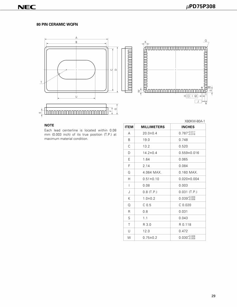
X80KW-80A-1
ITEM MILLIMETERS INCHES
NOTE
Each lead centerline is located within 0.08 mm (0.003 inch) of its true position (T.P.) at maximum material condition.
A
B
C
D
E
F
G
H
I
J
K
Q
R
S
T
U
W
20.0±0.4
19.0
13.2
14.2±0.4
1.64
2.14
4.064 MAX.
0.51±0.10
0.08
0.8 (T.P.)
1.0±0.2
C 0.5
0.8
1.1
R 3.0
12.0
0.75±0.2
0.787
0.748
0.520
0.559±0.016
0.065
0.084
0.160 MAX.
0.020±0.004
0.003
0.031 (T.P.)
0.039
C 0.020
0.031
0.043
R 0.118
0.472
0.030
+0.017–0.016
+0.009–0.008
+0.008–0.009
80 PIN CERAMIC WQFN
A
B
DC
T
U
F
I M
E
G
K Q
J
80
R
1H
SW

µPD75P308
30
6. RECOMMENDED SOLDERING CONDITIONS
It is recommended that µPD75P308 be soldered under the following conditions.
For details on the recommended soldering conditions, refer to Information Document "Semiconductor
Devices Mounting Manual" (IEI-616).
The soldering methods and conditions are not listed here, consult NEC.
Table 6-1 Soldering Conditions
µPD75P308GF-3B9: 80-pin plastic QFP (14 x 20 mm)
Soldering Method Soldering Conditions Symbol for RecommendedCondition
Wave Soldering Soldering bath temperature: 260°C max., WS60-162-1time: 10 seconds max., number of times: 1,pre-heating temperature: 120°C max. (package surfacetemperature), maximum number of days: 2 days*,(beyond this period, 16 hours of pre-baking is requiredat 125°C).
Infrared Reflow Package peak temperature: 230°C, IR30-162-1time: 30 seconds max. (210°C min.),number of times: 1, maximum number of days: 2 days*(beyond this period, 16 hours of pre-baking is requiredat 125°C)
VPS Package peak temperature: 215°C, VP15-162-1time: 40 seconds max. (200°C min.),number of times: 1, maximum number of days: 2 days*(beyond this period, 16 hours of pre-baking is requiredat 125°C)
Pin Partial Heating Pin temperature: 300°C max., —time: 3 seconds max. (per side)
*: Number of days after unpacking the dry pack. Storage conditions are 25°C and 65%RH max.
Caution: Do not use two or more soldering methods in combination (except the pin partial heating
method).
A model that can be soldered under the more stringent conditions (infrared reflow peak
temperature: 235°C, number of times: 2, and an extended number of days) is also available.
For details, consult NEC.
Notice

µPD75P308
31
Hardare IE-75000-R*1 In-circuit emulator for 75K series
IE-75001-R
IE-75000-R-EM*2 Emulation board for IE-75000-R and IE-75001-R
EP-75308GF-R Emulation prove for µPD75P308GF, provided with 80-pin conversion socket,
EV-9200G-80.
PG-1500 PROM programmer
PA-75P308GF PROM programmer adapter solely used for µPD75P308GF. It is connected to
PG-1500.
PA-75P308K PROM programmer adapter solely used for µPD75P308K. It is connected to
PG-1500.
Software IE Control Program Host machine
PG-1500 Controller • PC-9800 series (MS-DOSTM Ver.3.30 to Ver.5.00A*3)
RA75X Relocatable • IBM PC/ATTM (PC DOSTM Ver.3.1)
Assembler
APPENDIX A. DEVELOPMENT TOOLS
The following development support tools are readily available to support development of systems using
µPD75P308:
PROM writing tools
EV-9200G-80
*1: Maintenance product
2: Not provided with IE-75001-R
3: Ver.5.00/5.00A has a task swap function, but this function cannot be used with this software.
Remarks: For development tools from other companies, refer to 75X Series Selection Guide (IF-151).
µPD75P308
32
APPENDIX B. RELATED DOCUMENTS

µPD75P308
33
GENERAL NOTES ON CMOS DEVICES
1 STATIC ELECTRICITY (ALL MOS DEVICES)
Exercise care so that MOS devices are not adversely influenced by static electricity while being
handled.
The insulation of the gates of the MOS device may be destroyed by a strong static charge.
Therefore, when transporting or storing the MOS device, use a conductive tray, magazine case,
or conductive buffer materials, or the metal case NEC uses for packaging and shipment, and use
grounding when assembling the MOS device system. Do not leave the MOS device on a plastic
plate and do not touch the pins of the device.
Handle boards on which MOS devices are mounted similarly .
2 PROCESSING OF UNUSED PINS (CMOS DEVICES ONLY)
Fix the input level of CMOS devices.
Unlike bipolar or NMOS devices, if a CMOS device is operated with nothing connected to its
input pin, intermediate level input may be generated due to noise, and an inrush current may flow
through the device, causing the device to malfunction. Therefore, fix the input level of the device
by using a pull-down or pull-up resistor. If there is a possibility that an unused pin serves as an
output pin (whose timing is not specified), each pin should be connected to VDD or GND through
a resistor.
Refer to “Processing of Unused Pins” in the documents of each devices.
3 STATUS BEFORE INITIALIZATION (ALL MOS DEVICES)
The initial status of MOS devices is undefined upon power application.
Since the characteristics of an MOS device are determined by the quantity of injection at the
molecular level, the initial status of the device is not controlled during the production process. The
output status of pins, I/O setting, and register contents upon power application are not guaranteed.
However, the items defined for reset operation and mode setting are subject to guarantee after
the respective operations have been executed.
When using a device with a reset function, be sure to reset the device after power application.
µPD75P308
34
[MEMO]
No part of this document may be copied or reproduced in any form or by any means without the prior
written consent of NEC Corporation. NEC Corporation assumes no responsibility for any errors which
may appear in this document.
NEC Corporation does not assume any liability for infringement of patents, copyrights or other
intellectual property rights of third parties by or arising from use of a device described herein or any other
liability arising from use of such device. No license, either express, implied or otherwise, is granted
under any patents, copyrights or other intellectual property rights of NEC Corporation or others.
The devices listed in this document are not suitable for uses in aerospace equipment, submarine cables,
nuclear reactor control systems and life support systems. If customers intend to use NEC devices for
above applications or they intend to use "Standard" quality grade NEC devices for the applications not
intended by NEC, please contact our sales people in advance.
Application examples recommended by NEC Corporation
Standard: Computer, Office equipment, Communication equipment, Test and Measurement equipment,
Machine tools, Industrial robots, Audio and Visual equipment, Other consumer products,etc.
Special: Automotive and Transportation equipment, Traffic control systems, Antidisaster systems,
Anticrime system, etc.
MS-DOS is a trademark of Microsoft Corporation.
PC DOS and PC/AT are trademarks of IBM Corporation.
M4 92.6
Related Documents
. şi filtrând ... circuit](https://static.cupdf.com/doc/110x72/5b94eb5b09d3f2c2678b61c6/ihiijuai-qsl-circuite-sunt-acordate-sincron-cu-ajutorul-condensatorului.jpg)