EE141 – Fall 2005 Lecture 6 MOS Capacitances, MOS Capacitances, Propagation Delay Propagation Delay EE141 2 Important! Check course home page periodically for announcements Homework 2 is due TODAY by 5pm • In 240 Cory Homework 3 will be posted TODAY • Due Thursday Sep 22 by 5pm

Welcome message from author
This document is posted to help you gain knowledge. Please leave a comment to let me know what you think about it! Share it to your friends and learn new things together.
Transcript

1
EE141 – Fall 2005Lecture 6
MOS Capacitances,MOS Capacitances,Propagation DelayPropagation Delay
EE141 2
Important!
Check course home page periodically for announcements
Homework 2 is due TODAY by 5pm• In 240 Cory
Homework 3 will be posted TODAY• Due Thursday Sep 22 by 5pm

2
EE141 3
Today’s Lecture
The MOS transistor characteristics for transient analysis
Propagation delay
EE141 4
Review
MOS Transistor ModelMOS Transistor Model
CMOS Inverter VTCCMOS Inverter VTC

3
EE141 5
Important to Remember!
0 0.5 1 1.5 2 2.50
0.5
1
1.5
2
2.5x 10
-4
VDS (V)
I D(A
)
VelocitySaturation
VDS = VGT
VDSAT = VGT
Saturation
Linear
VDS = VDSAT
LinearRelationship
QuadraticRelationship
EE141 6
A Unified Model for Manual Analysis
B
D
G
ID
S
( )DSGTD VVVVL
WkI ⋅+⋅
−⋅⋅⋅= λ1
2'
2min
min
for VGT ≤ 0: ID = 0
with Vmin = min (VGT, VDS, VDSAT)
for VGT ≥ 0:
define VGT = VGS – VT
4
EE141 7
VDSp
IDp
VGSp = -2.5
VGSp = -1VDSp
IDnVin= 0
Vin= 1.5
Vout
IDnVin= 0
Vin= 1.5
Vout
IDn
PMOS Load Lines
Vin = VDD + VGSpIDn = -IDp
Vout = VDD + VDSp
Vin = VDD + VGSpIDn = -IDpVout = VDD + VDSp
Coordinate transform: IDp (VDSp) → IDn (Vout)
EE141 8
IDn
Vout
Vin = 2.5
Vin = 2
Vin = 1.5
Vin = 0
Vin = 0.5
Vin = 1
NMOS
Vin = 0
Vin = 0.5
Vin = 1Vin = 1.5
Vin = 2
Vin = 2.5
Vin = 1Vin = 1.5
PMOS
CMOS Inverter Load Characteristics

5
EE141 9
CMOS Inverter VTC
Vin0.5 1 1.5 2 2.5
NMOS resPMOS off
NMOS satPMOS sat
NMOS offPMOS res
NMOS satPMOS res
NMOS resPMOS sat0.5
1
1.5
2
2.5
Vout
EE141 10
Inverter Gain
0 0.5 1 1.5 2 2.5-18
-16
-14
-12
-10
-8
-6
-4
-2
0
Vin (V)
gain
pn
DSATppDSATnn
MD
VkVkVI
gλλ −
⋅+⋅⋅−=
)(1
)()2(1
pnDSATnTnM VVVrg
λλ −⋅−−+
≈
6
EE141 11
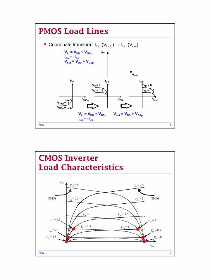
Gain as a function of VDD
0 0.5 1 1.5 2 2.50
0.5
1
1.5
2
2.5
Vin (V)
Vou
t(V)
Vin (V)
V out
(V)
0 0.05 0.1 0.15 0.20
0.05
0.1
0.15
0.2
Vin (V)
Vou
t (V)
Vin (V)V o
ut(V
)
Gain = -1
EE141 12
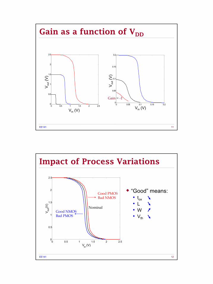
Impact of Process Variations
0 0.5 1 1.5 2 2.50
0.5
1
1.5
2
2.5
Vin (V)
V out(V
)
Good PMOSBad NMOS
Good NMOSBad PMOS
Nominal
“Good” means:• tox• L• W• Vth

7
EE141 13
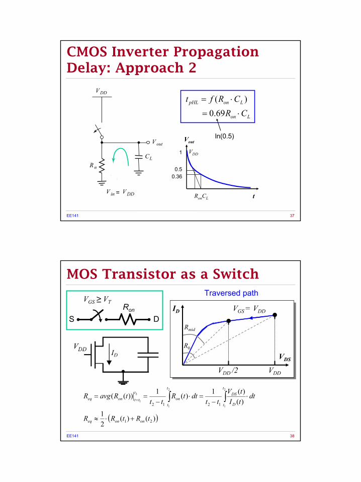
Outline
Dynamic Operation of Dynamic Operation of MOS TransistorMOS Transistor• MOS Capacitances• Propagation Delay
EE141 14
DS
G
B
CGDCGS
CSB CDBCGB
MOS Capacitances
8
EE141 15
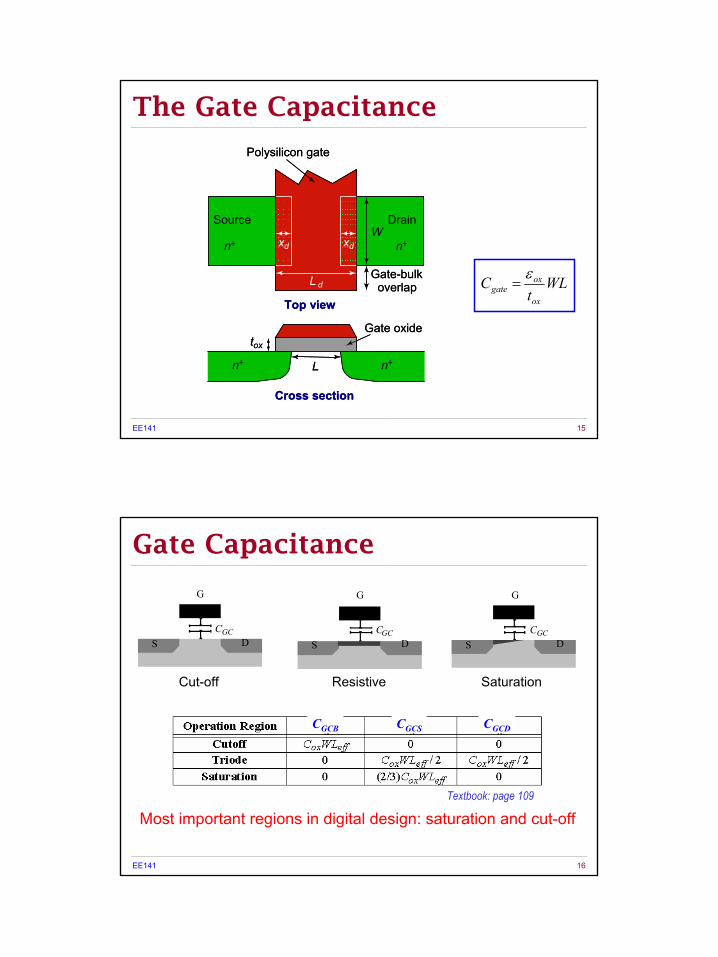
The Gate Capacitance
WLt
Cox
oxgate
ε=
tox
n+ n+
Cross section
L
Gate oxidetox
n+ n+
Cross section
L
Gate oxide
xd xd
L d
Polysilicon gate
Top view
Gate-bulkoverlap
Source
n+
Drain
n+W
xd xd
L d
Polysilicon gate
Top view
Gate-bulkoverlap
Source
n+
Drain
n+W
EE141 16
Gate Capacitance
S D
G
CGC
S D
G
CGCS D
G
CGC
Cut-off Resistive Saturation
Most important regions in digital design: saturation and cut-offTextbook: page 109
CGCB CGCS CGCD

9
EE141 17
Cgate as a function of VGS(with VDS = 0)
Cgate as a function of the degree of saturation
Gate Capacitance
0 1VDS / (VGS – VT)
CGC
CGCS
CGCD
WLCox2WLCox
2
3WLCox
WLCox
2WLCox
VGS
CGC
CGCS=CGCDCGCB
EE141 18
Measuring the Gate Cap
VGS
I
-1.5 -1 -0.5 0
3
4
5
6
7
8
9
10x 10 -16
2
G a t e C a p a c i t a n c e ( F )
0.5 1 1.5 2-2
Cap
acita
nce
(F)
VGS (V)

10
EE141 19
Diffusion Capacitance
Bottom
Side wall
Side wallChannel
Source
Channel-stop implant
Substrate
W
NA+
NA
LS
ND
xj
Cdiff = Cbottom + Csw
= Cj · AREA + Cjsw · PERIMETER= Cj·LSW + Cjsw(2LS + W)
EE141 20
Junction Capacitance
mD
jj V
CC
)1( 0
0
φ−= m = 0.5: abrupt junction
m = 0.33: linear junction
11
EE141 21
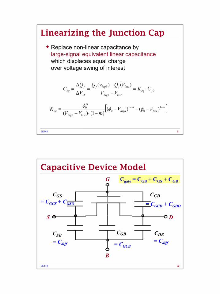
Linearizing the Junction Cap
Replace non-linear capacitance bylarge-signal equivalent linear capacitancewhich displaces equal charge over voltage swing of interest
0
)()(jeq
lowhigh
lowjhighj
D
jeq CK
VVVQvQ
VQ
C ⋅=−
−=
∆
∆=
[ ]mlow
mhigh
lowhigh
m
eq VVmVV
K −− −−−−⋅−
−= 1
01
00 )()(
)1()(φφφ
EE141 22
CGDCGS
CSB CDBCGB
Cgate = CGB + CGS + CGD
Capacitive Device Model
= CGCS + CGSO = CGCD + CGDO
= CGCB= Cdiff
G
S D
B
= Cdiff

12
EE141 23
Capacitances in 0.25µm CMOS Process
Textbook: page 112
EE141 24
.MODEL Parameters MOS1
.MODEL Modname NMOS/PMOS <VT0=VT0…>
13
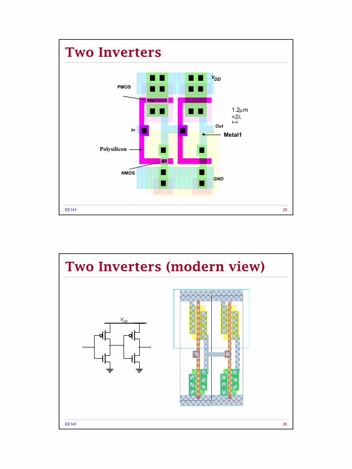
EE141 25
Polysilicon
InOut
Metal1
VDD
GND
PMOS
NMOS
Two Inverters
1.2µm=2λ
EE141 26
VDD
Two Inverters (modern view)

14
EE141 27
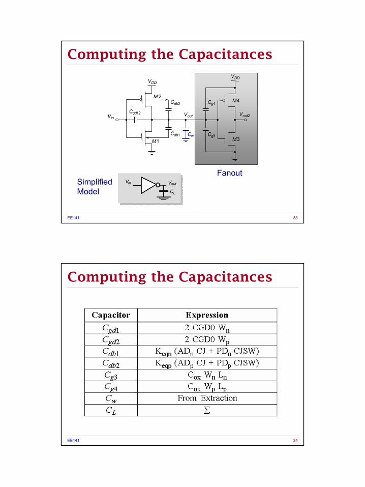
FanoutVoutVin
CL
SimplifiedModel
M3
M4
M1
M 2
Cw Cg3Cdb1
Cg4
Vout2
Cdb2
VDDVDD
VinVout
Cgd12
Computing the Capacitances
EE141 28
The CMOS Inverter: Cin
Cgdn,p
Cgsp
Cgsn
S
G D
S
VoutVinCinCL
15
EE141 29
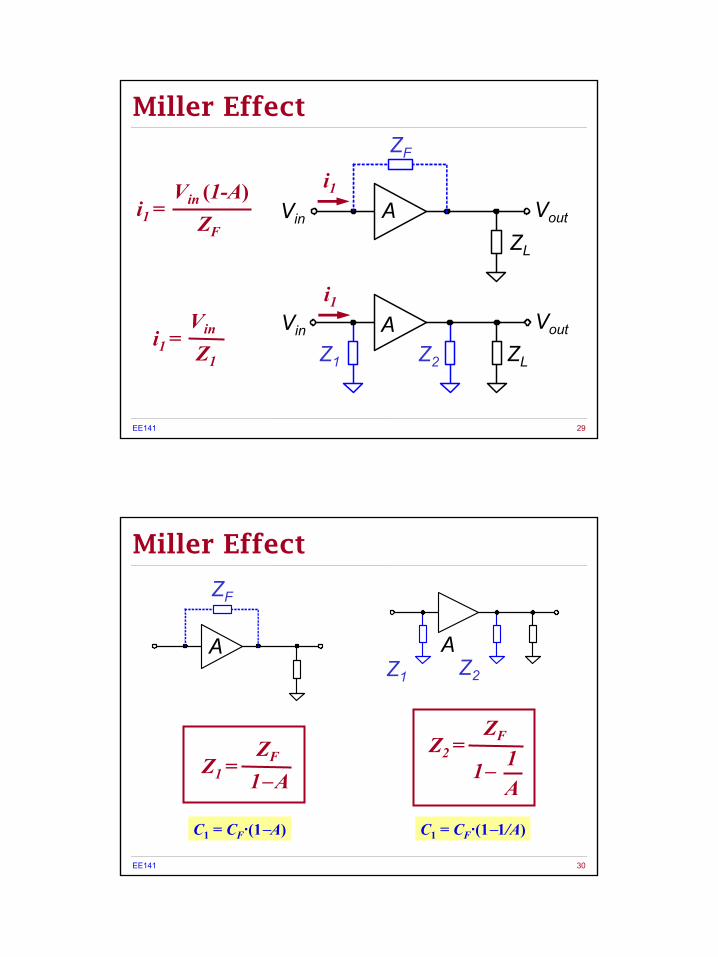
Miller Effect
VoutVin
ZL
ZF
Ai1
A VoutVin
i1
Z1 Z2 ZL
i1 =Vin (1-A)
ZF
i1 =Vin
Z1
EE141 30
Miller Effect
ZF
A AZ1 Z2
Z1 =ZF
1−A
Z2 =ZF
1A
1−
C1 = CF·(1−A) C1 = CF·(1−1/A)

16
EE141 31
CMOS Inverter Example: Cin
Cgd
Cgsp
Cgsn
CinA = -1
Cgs = Cgsn + Cgsp
Cgd = Cgdn + Cgdp
Cin = Cgs + Cgd (1-A)
+∆V -∆V
EE141 32
Vin
M1
Cgd1Vout
∆V
∆V
Vin
M1
Vout ∆V
∆V
2Cgd1
The Miller Effect
“A capacitor experiencing identical but opposite voltage swingat both terminals can be replaced by a capacitor to ground,whose value is two times the original value”
2Cgd1
17
EE141 33
FanoutVoutVin
CL
SimplifiedModel
M3
M4
M1
M 2
Cw Cg3Cdb1
Cg4
Vout2
Cdb2
VDDVDD
VinVout
Cgd12
Computing the Capacitances
EE141 34
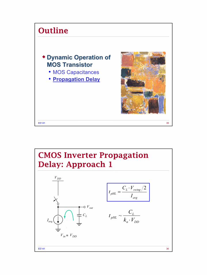
Computing the Capacitances
18
EE141 35
Outline
Dynamic Operation of Dynamic Operation of MOS TransistorMOS Transistor• MOS Capacitances• Propagation Delay
EE141 36
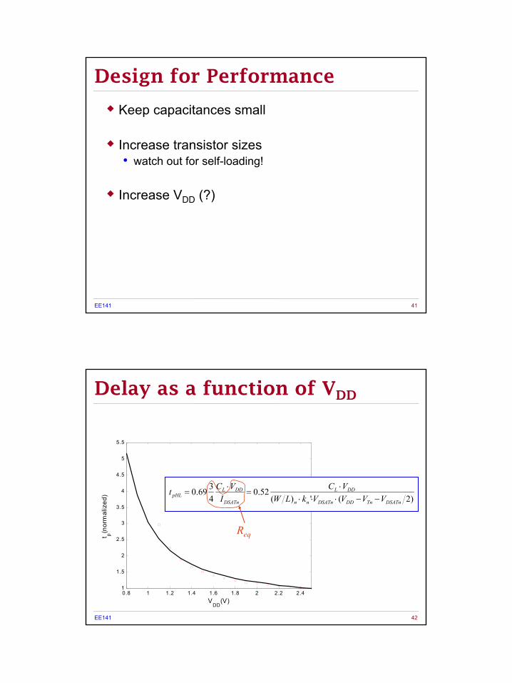
CMOS Inverter Propagation Delay: Approach 1
V out
Iavg
V DD
V in = V DD
CL
avg
swingLpHL I
VCt
2⋅=
DDn
LpHL Vk
Ct⋅
~
19
EE141 37
CMOS Inverter Propagation Delay: Approach 2
V out
R n
V DD
V in = V DD
CL
)( LonpHL CRft ⋅=
Lon CR ⋅= 69.0
0.360.5
1
RonCL t
Voutln(0.5)
VDD
EE141 38
MOS Transistor as a SwitchTraversed path
ID
VDS
VDDVDD /2
VGS = VDD
Rmid
R0
∫∫ ⋅−
=⋅−
===
2
1
2
1
2
1 )()(1)(1))((
1212
t
t D
DSt
ton
t
ttoneq dttItV
ttdttR
tttRavgR
( ))()(21
21 tRtRR ononeq +⋅≈
VGS ≥ VT
S DRon

20
EE141 39
The Transistor as a Switch
VGS ≥ VT
S DRon
( ) ( )
⋅+⋅
+⋅+⋅
⋅=21
212
1
DDDSAT
DD
DDDSAT
DDeq VI
VVI
VRλλ
⋅⋅−⋅≈ DD
DSAT
DDeq V
IVR λ
651
43
ID
VDS
VDDVDD /2
VGS = VDD
Rmid
R0
( )021 RRR mideq +⋅=
EE141 40
0 0.5 1 1.5 2 2.5
x 10-10
-0.5
0
0.5
1
1.5
2
2.5
3
t (sec)
Vou
t(V)
tp = 0.69 CL·(Reqn+Reqp)/2?
tpLH
tpHL
Transient Response
21
EE141 41
Design for Performance
Keep capacitances small
Increase transistor sizes• watch out for self-loading!
Increase VDD (?)
EE141 42
0.8 1 1.2 1.4 1.6 1.8 2 2.2 2.41
1.5
2
2.5
3
3.5
4
4.5
5
5.5
VDD
(V)
t p(nor
mal
ized
)
Delay as a function of VDD
)2(')(52.0
4369.0
DSATnTnDDDSATnnn
DDL
DSATn
DDLpHL VVVVkLW
VCI
VCt−−⋅⋅⋅
⋅=
⋅=
Req

22
EE141 43
2 4 6 8 10 12 142
2.2
2.4
2.6
2.8
3
3.2
3.4
3.6
3.8x 10
-11
S
t p(sec
)
Device Sizing
(fixed load)
Self-loading effect:Intrinsic capacitancesdominate
EE141 44
1 1.5 2 2.5 3 3.5 4 4.5 53
3.5
4
4.5
5x 10
-11
β
t p(sec
)
NMOS/PMOS Ratio
tpLH tpHL
tp β = Wp/Wn

23
EE141 45
t pH
L(ns
ec)
0.35
0.3
0.25
0.2
0.15
trise (nsec)10.80.60.40.20
tp = tstep(i) + η·tstep(i-1)
Impact of Rise Time on Delay
EE141 46
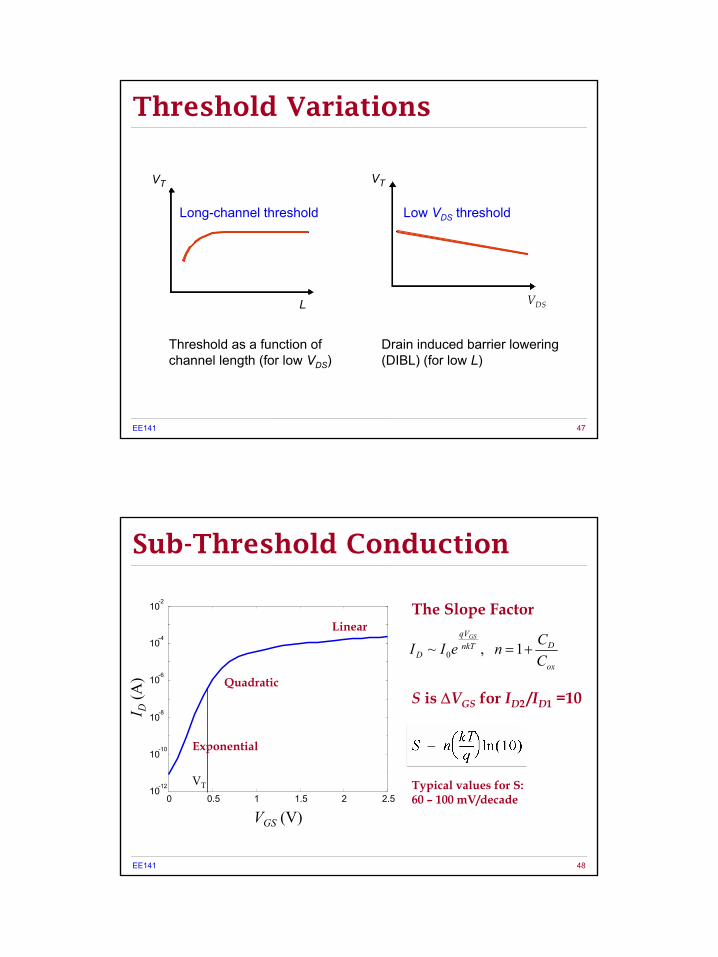
Threshold Variations
Sub-threshold Conduction
Parasitic Resistances
The Sub-Micron MOS Transistor
24
EE141 47
VT
L
Long-channel threshold
Threshold as a function ofchannel length (for low VDS)
VDS
VT
Threshold Variations
Low VDS threshold
Drain induced barrier lowering (DIBL) (for low L)
EE141 48
Sub-Threshold Conduction
Typical values for S:60 – 100 mV/decade
The Slope Factor
ox
DnkTqV
D CCneII
GS
+=1 ,~ 0
S is ∆VGS for ID2 /ID1 =10
0 0.5 1 1.5 2 2.510
-12
10-10
10-8
10-6
10-4
10-2
VT
Linear
Exponential
Quadratic
VGS (V)
I D(A
)
25
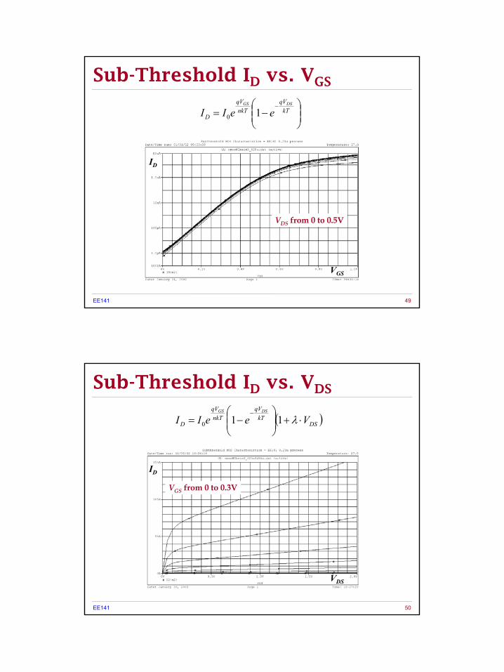
EE141 49
VDS from 0 to 0.5V
−=
−kT
qVnkT
qV
D
DSGS
eeII 10
Sub-Threshold ID vs. VGS
ID
VGS
EE141 50
Sub-Threshold ID vs. VDS
( )DSkT
qVnkT
qV
D VeeIIDSGS
⋅+
−=
−λ110
VGS from 0 to 0.3V
ID
VDS
26
EE141 51
Next Lecture
Optimizing for Performance
Power dissipation in CMOS inverters
Related Documents