HEF4047B Monostable/astable multivibrator Rev. 6 — 17 March 2017 Product data sheet 1 General description The HEF4047B is a retriggerable astable multivibrator that can be configured as either a positive-edge or negative-edge triggered monostable multivibrator. The output pulse width is programmed by selection of external components (R t and C t ). Inputs include clamp diodes. This enables the use of current limiting resistors to interface inputs to voltages in excess of V CC . 2 Features and benefits 2.1 General • Monostable (one-shot) or astable (free-running) operation • True and complemented buffered outputs • Only one external resistor and capacitor required 2.2 Monostable multivibrator • Positive- or negative-edge triggering • Output pulse width independent of trigger pulse duration • Retriggerable option for pulse-width expansion • Long pulse width possible using small RC components with external counter provision • Fast recovery time independent of pulse width • Pulse-width accuracy maintained at duty cycles approaching 100% 2.3 Astable multivibrator • Free-running or gatable operating modes • 50% duty cycle • Oscillator output available 3 Ordering information Table 1. Ordering information Package Type number Name Description Version HEF4047BT SO14 plastic small outline package; 14 leads; body width 3.9 mm SOT108-1

Welcome message from author
This document is posted to help you gain knowledge. Please leave a comment to let me know what you think about it! Share it to your friends and learn new things together.
Transcript
HEF4047BMonostable/astable multivibratorRev. 6 — 17 March 2017 Product data sheet
1 General description
The HEF4047B is a retriggerable astable multivibrator that can be configured as eithera positive-edge or negative-edge triggered monostable multivibrator. The output pulsewidth is programmed by selection of external components (Rt and Ct). Inputs includeclamp diodes. This enables the use of current limiting resistors to interface inputs tovoltages in excess of VCC.
2 Features and benefits
2.1 General• Monostable (one-shot) or astable (free-running) operation• True and complemented buffered outputs• Only one external resistor and capacitor required
2.2 Monostable multivibrator• Positive- or negative-edge triggering• Output pulse width independent of trigger pulse duration• Retriggerable option for pulse-width expansion• Long pulse width possible using small RC components with external counter provision• Fast recovery time independent of pulse width• Pulse-width accuracy maintained at duty cycles approaching 100%
2.3 Astable multivibrator• Free-running or gatable operating modes• 50% duty cycle• Oscillator output available
3 Ordering informationTable 1. Ordering information
PackageType number
Name Description VersionHEF4047BT SO14 plastic small outline package; 14 leads; body width 3.9 mm SOT108-1
Nexperia HEF4047BMonostable/astable multivibrator
HEF4047B All information provided in this document is subject to legal disclaimers. © Nexperia B.V. 2017. All rights reserved.
Product data sheet Rev. 6 — 17 March 20172 / 22
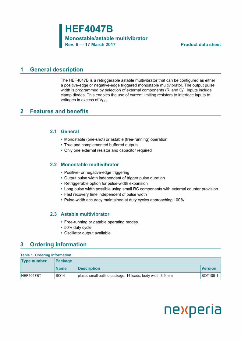
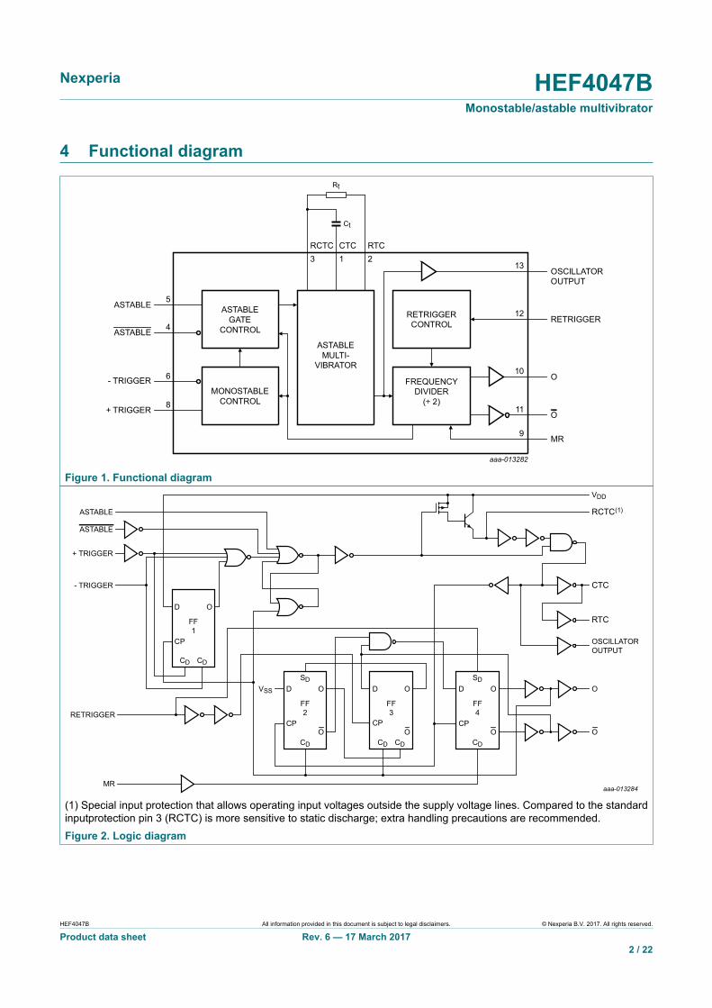
4 Functional diagram
aaa-013282
13
MR
O
O
RETRIGGER
OSCILLATOROUTPUT
ASTABLE
ASTABLE
- TRIGGER
+ TRIGGER
12RETRIGGERCONTROL
ASTABLEMULTI-
VIBRATOR
ASTABLEGATE
CONTROL
MONOSTABLECONTROL
FREQUENCYDIVIDER
(÷ 2)
10
11
9
Rt
Ct
RCTC CTC RTC3
5
4
6
8
1 2
Figure 1. Functional diagram
aaa-013284
D
VDD
CTC
RTC
OSCILLATOROUTPUT
O
O
RCTC(1)
VSS
CD
CP
FF2
O
MR
RETRIGGER
- TRIGGER
+ TRIGGER
ASTABLE
ASTABLE
DSD
CD CD
CP
FF3
O DSD
CD
CP
FF4
O
OOO
D
CD
CP
FF1
O
CD
(1) Special input protection that allows operating input voltages outside the supply voltage lines. Compared to the standardinputprotection pin 3 (RCTC) is more sensitive to static discharge; extra handling precautions are recommended.Figure 2. Logic diagram
Nexperia HEF4047BMonostable/astable multivibrator
HEF4047B All information provided in this document is subject to legal disclaimers. © Nexperia B.V. 2017. All rights reserved.
Product data sheet Rev. 6 — 17 March 20173 / 22
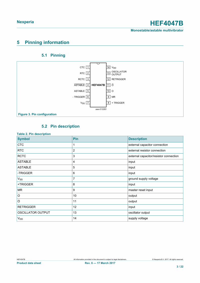
5 Pinning information
5.1 Pinning
HEF4047B
CTC VDD
RTCOSCILLATOROUTPUT
RCTC RETRIGGER
ASTABLE O
ASTABLE O
- TRIGGER MR
VSS + TRIGGER
aaa-013283
1
2
3
4
5
6
7 8
10
9
12
11
14
13
Figure 3. Pin configuration
5.2 Pin description
Table 2. Pin descriptionSymbol Pin DescriptionCTC 1 external capacitor connection
RTC 2 external resistor connection
RCTC 3 external capacitor/resistor connection
ASTABLE 4 input
ASTABLE 5 input
-TRIGGER 6 input
VSS 7 ground supply voltage
+TRIGGER 8 input
MR 9 master reset input
O 10 output
O 11 output
RETRIGGER 12 input
OSCILLATOR OUTPUT 13 oscillator output
VDD 14 supply voltage
Nexperia HEF4047BMonostable/astable multivibrator
HEF4047B All information provided in this document is subject to legal disclaimers. © Nexperia B.V. 2017. All rights reserved.
Product data sheet Rev. 6 — 17 March 20174 / 22
6 Functional description
The HEF4047B consists of a gate-able astable multivibrator incorporating logictechniques to permit positive or negative edge-triggered monostable multivibrator actionwith retriggering and external counting options.
Inputs include +TRIGGER, −TRIGGER, ASTABLE, ASTABLE, RETRIGGER and MR(master reset). Buffered outputs are O, O and OSCILLATOR OUTPUT. In all modes ofoperation an external capacitor (Ct) must be connected between CTC and RCTC, and anexternal resistor (Rt) must be connected between RTC and RCTC.
A HIGH level on the ASTABLE input enables astable operation. The period of the squarewave at O and O outputs is a function of the external components employed. ‘True’ inputpulses on the ASTABLE or ‘complement’ pulses on the ASTABLE input, allow the circuitto be used as a gate-able multivibrator. The OSCILLATOR OUTPUT period is half ofthe O output in the astable mode. However, a 50% duty factor is not guaranteed at thisoutput.
In the monostable mode, positive edge-triggering is accomplished by applying a leading-edge pulse to the +TRIGGER input and a LOW level to the −TRIGGER input. Fornegative edge-triggering, a trailing-edge pulse is applied to the −TRIGGER and a HIGHlevel to the +TRIGGER. Input pulses may be of any duration relative to the output pulse.The multivibrator can be retriggered (on the leading-edge only) by applying a commonpulse to both the RETRIGGER and +TRIGGER inputs. In this mode, the output pulseremains HIGH as long as the input pulse period is shorter than the period determined bythe RC components.
An external count down option implements coupling O to an external ‘N’ counter andresetting the counter with the trigger pulse. The counter output pulse is fed back to theASTABLE input and has a duration equal to N times the period of the multivibrator. AHIGH level on the MR input assures no output pulse during an ON-power condition. Thisinput can also be activated to terminate the output pulse at any time. In the monostablemode, a HIGH level or power-ON reset pulse must be applied to MR, whenever VDD isapplied.
Nexperia HEF4047BMonostable/astable multivibrator
HEF4047B All information provided in this document is subject to legal disclaimers. © Nexperia B.V. 2017. All rights reserved.
Product data sheet Rev. 6 — 17 March 20175 / 22
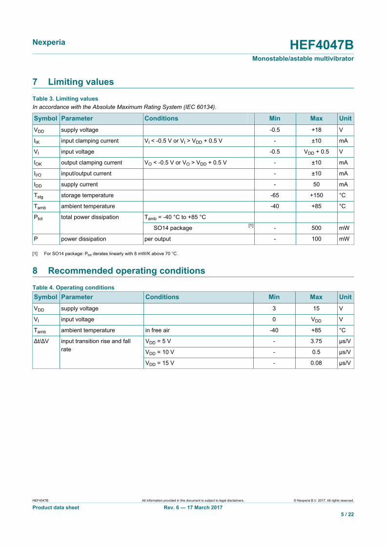
7 Limiting valuesTable 3. Limiting valuesIn accordance with the Absolute Maximum Rating System (IEC 60134).
Symbol Parameter Conditions Min Max UnitVDD supply voltage -0.5 +18 V
IIK input clamping current VI < -0.5 V or VI > VDD + 0.5 V - ±10 mA
VI input voltage -0.5 VDD + 0.5 V
IOK output clamping current VO < -0.5 V or VO > VDD + 0.5 V - ±10 mA
II/O input/output current - ±10 mA
IDD supply current - 50 mA
Tstg storage temperature -65 +150 °C
Tamb ambient temperature -40 +85 °C
Tamb = -40 °C to +85 °CPtot total power dissipation
SO14 package [1] - 500 mW
P power dissipation per output - 100 mW
[1] For SO14 package: Ptot derates linearly with 8 mW/K above 70 °C.
8 Recommended operating conditionsTable 4. Operating conditionsSymbol Parameter Conditions Min Max UnitVDD supply voltage 3 15 V
VI input voltage 0 VDD V
Tamb ambient temperature in free air -40 +85 °C
VDD = 5 V - 3.75 μs/V
VDD = 10 V - 0.5 μs/V
Δt/ΔV input transition rise and fallrate
VDD = 15 V - 0.08 μs/V
Nexperia HEF4047BMonostable/astable multivibrator
HEF4047B All information provided in this document is subject to legal disclaimers. © Nexperia B.V. 2017. All rights reserved.
Product data sheet Rev. 6 — 17 March 20176 / 22
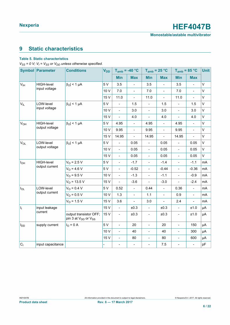
9 Static characteristicsTable 5. Static characteristicsVSS = 0 V; VI = VSS or VDD unless otherwise specified.
Tamb = -40 °C Tamb = 25 °C Tamb = 85 °CSymbol Parameter Conditions VDD
Min Max Min Max Min Max
Unit
5 V 3.5 - 3.5 - 3.5 - V
10 V 7.0 - 7.0 - 7.0 - V
VIH HIGH-levelinput voltage
|IO| < 1 μA
15 V 11.0 - 11.0 - 11.0 - V
5 V - 1.5 - 1.5 - 1.5 V
10 V - 3.0 - 3.0 - 3.0 V
VIL LOW-levelinput voltage
|IO| < 1 μA
15 V - 4.0 - 4.0 - 4.0 V
5 V 4.95 - 4.95 - 4.95 - V
10 V 9.95 - 9.95 - 9.95 - V
VOH HIGH-leveloutput voltage
|IO| < 1 μA
15 V 14.95 - 14.95 - 14.95 - V
5 V - 0.05 - 0.05 - 0.05 V
10 V - 0.05 - 0.05 - 0.05 V
VOL LOW-leveloutput voltage
|IO| < 1 μA
15 V - 0.05 - 0.05 - 0.05 V
VO = 2.5 V 5 V - -1.7 - -1.4 - -1.1 mA
VO = 4.6 V 5 V - -0.52 - -0.44 - -0.36 mA
VO = 9.5 V 10 V - -1.3 - -1.1 - -0.9 mA
IOH HIGH-leveloutput current
VO = 13.5 V 15 V - -3.6 - -3.0 - -2.4 mA
VO = 0.4 V 5 V 0.52 - 0.44 - 0.36 - mA
VO = 0.5 V 10 V 1.3 - 1.1 - 0.9 - mA
IOL LOW-leveloutput current
VO = 1.5 V 15 V 3.6 - 3.0 - 2.4 - mA
15 V - ±0.3 - ±0.3 - ±1.0 μAII input leakagecurrent
output transistor OFF;pin 3 at VDD or VSS
15 V - ±0.3 - ±0.3 - ±1.0 μA
5 V - 20 - 20 - 150 μA
10 V - 40 - 40 - 300 μA
IDD supply current IO = 0 A
15 V - 80 - 80 - 600 μA
CI input capacitance - - - - 7.5 - - pF

Nexperia HEF4047BMonostable/astable multivibrator
HEF4047B All information provided in this document is subject to legal disclaimers. © Nexperia B.V. 2017. All rights reserved.
Product data sheet Rev. 6 — 17 March 20177 / 22
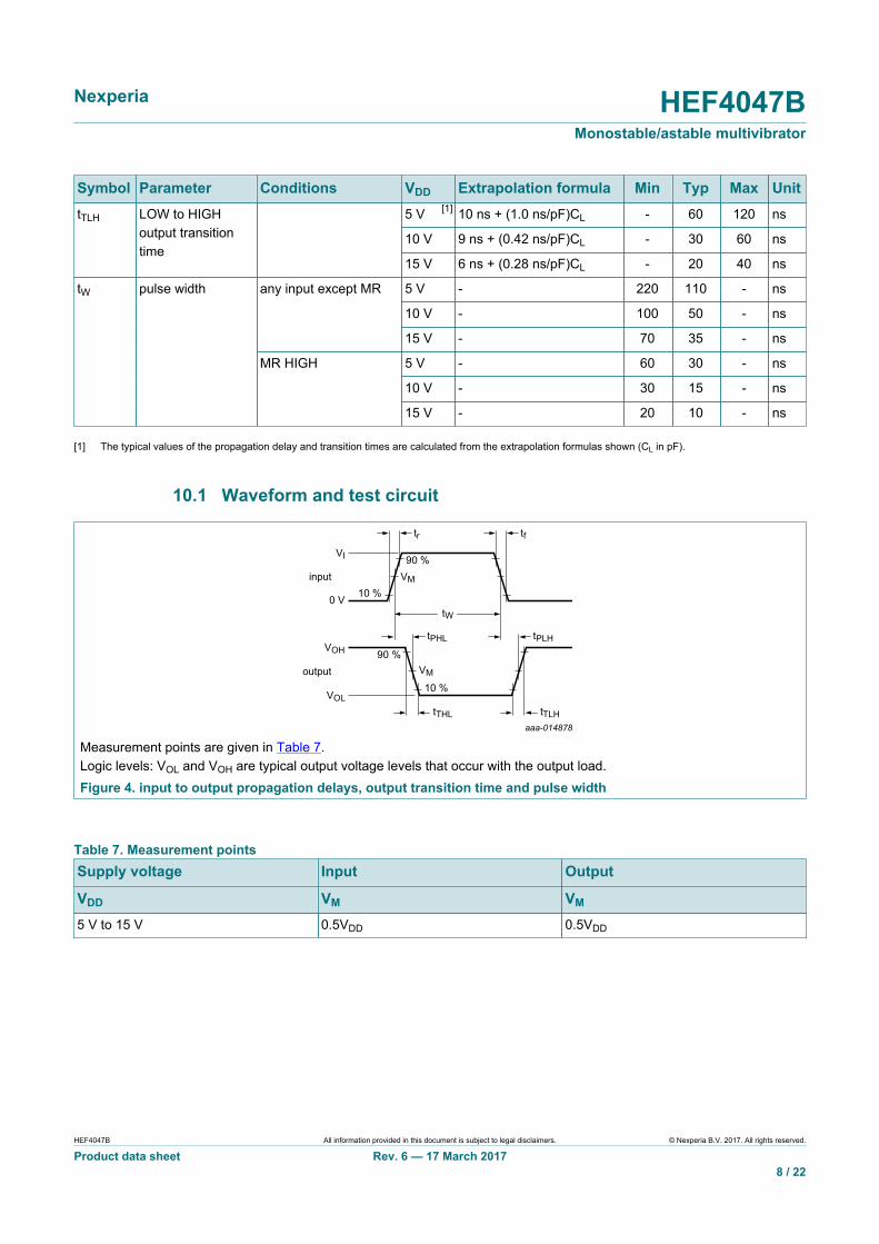
10 Dynamic characteristicsTable 6. Dynamic characteristicsVSS = 0 V; Tamb = 25 °C; unless otherwise specified; for waveform and test circuit, see Figure 4 and Figure 5.
Symbol Parameter Conditions VDD Extrapolation formula Min Typ Max Unit5 V [1] 68 ns + (0.55 ns/pF)CL - 95 190 ns
10 V [1] 43 ns + (0.23 ns/pF)CL - 45 90 ns
tPHL HIGH to LOWpropagation delay
ASTABLE, ASTABLEto OSCILLATOROUTPUT
15 V [1] 22 ns + (0.16 ns/pF)CL - 30 60 ns
5 V [1] 58 ns + (0.55 ns/pF)CL - 85 170 ns
10 V 29 ns + (0.23 ns/pF)CL - 40 80 ns
tPLH LOW to HIGHpropagation delay
ASTABLE, ASTABLEto OSCILLATOROUTPUT
15 V 22 ns + (0.16 ns/pF)CL - 30 60 ns
5 V [1] 123 ns + (0.55 ns/pF)CL - 150 300 ns
10 V 54 ns + (0.23 ns/pF)CL - 65 130 ns
tPHL HIGH to LOWpropagation delay
ASTABLE, ASTABLEto O, O
15 V 42 ns + (0.16 ns/pF)CL - 50 100 ns
5 V [1] 103 ns + (0.55 ns/pF)CL - 130 260 ns
10 V 49 ns + (0.23 ns/pF)CL - 60 120 ns
tPLH LOW to HIGHpropagation delay
ASTABLE, ASTABLEto O, O
15 V 37 ns + (0.16 ns/pF)CL - 45 90 ns
5 V [1] 133 ns + (0.55 ns/pF)CL - 160 320 ns
10 V 54 ns + (0.23 ns/pF)CL - 65 130 ns
tPHL HIGH to LOWpropagation delay
+/-TRIGGER to O, O
15 V 42 ns + (0.16 ns/pF)CL - 50 100 ns
5 V [1] 128 ns + (0.55 ns/pF)CL - 155 310 ns
10 V 54 ns + (0.23 ns/pF)CL - 65 130 ns
tPLH LOW to HIGHpropagation delay
+/-TRIGGER to O, O
15 V 42 ns + (0.16 ns/pF)CL - 50 100 ns
5 V [1] 38 ns + (0.55 ns/pF)CL - 65 130 ns
10 V 19 ns + (0.23 ns/pF)CL - 30 60 ns
tPHL HIGH to LOWpropagation delay
+TRIGGER,RETRIGGER to O
15 V 17 ns + (0.16 ns/pF)CL - 25 50 ns
5 V [1] 68 ns + (0.55 ns/pF)CL - 95 190 ns
10 V 29 ns + (0.23 ns/pF)CL - 40 80 ns
tPLH LOW to HIGHpropagation delay
+TRIGGER,RETRIGGER to O
15 V 22 ns + (0.16 ns/pF)CL - 30 60 ns
5 V [1] 83 ns + (0.55 ns/pF)CL - 100 200 ns
10 V 34 ns + (0.23 ns/pF)CL - 45 90 ns
tPHL HIGH to LOWpropagation delay
MR to O
15 V 27 ns + (0.16 ns/pF)CL - 35 70 ns
5 V [1] 83 ns + (0.55 ns/pF)CL - 100 200 ns
10 V 34 ns + (0.23 ns/pF)CL - 45 90 ns
tPLH LOW to HIGHpropagation delay
MR to O
15 V 27 ns + (0.16 ns/pF)CL - 35 70 ns
5 V [1] 10 ns + (1.0 ns/pF)CL - 60 120 ns
10 V 9 ns + (0.42 ns/pF)CL - 30 60 ns
tTHL HIGH to LOWoutput transitiontime
15 V 6 ns + (0.28 ns/pF)CL - 20 40 ns
Nexperia HEF4047BMonostable/astable multivibrator
HEF4047B All information provided in this document is subject to legal disclaimers. © Nexperia B.V. 2017. All rights reserved.
Product data sheet Rev. 6 — 17 March 20178 / 22
Symbol Parameter Conditions VDD Extrapolation formula Min Typ Max Unit5 V [1] 10 ns + (1.0 ns/pF)CL - 60 120 ns
10 V 9 ns + (0.42 ns/pF)CL - 30 60 ns
tTLH LOW to HIGHoutput transitiontime
15 V 6 ns + (0.28 ns/pF)CL - 20 40 ns
5 V - 220 110 - ns
10 V - 100 50 - ns
any input except MR
15 V - 70 35 - ns
5 V - 60 30 - ns
10 V - 30 15 - ns
tW pulse width
MR HIGH
15 V - 20 10 - ns
[1] The typical values of the propagation delay and transition times are calculated from the extrapolation formulas shown (CL in pF).
10.1 Waveform and test circuit
aaa-014878
input
output
tPLHtPHL
tW0 V
VI
VM
VM
VOH
VOLtTHL tTLH
90 %
10 %
10 %
90 %
tr tf
Measurement points are given in Table 7.Logic levels: VOL and VOH are typical output voltage levels that occur with the output load.Figure 4. input to output propagation delays, output transition time and pulse width
Table 7. Measurement pointsSupply voltage Input Output
VDD VM VM
5 V to 15 V 0.5VDD 0.5VDD
Nexperia HEF4047BMonostable/astable multivibrator
HEF4047B All information provided in this document is subject to legal disclaimers. © Nexperia B.V. 2017. All rights reserved.
Product data sheet Rev. 6 — 17 March 20179 / 22
VM VM
tW
tW
10 %
90 %
10 %
90 %
0 V
VI
VI
negativepulse
positivepulse
0 V
VM VM
90 %
10 %
90 %
10 %
tf
tr
tr
tf
001aaj781
a. Input waveform
001aaj915
VEXT
VDD
VI VODUT
CLRT
RL
G
b. Test circuit
Test and measurement data is given in Table 8.Definitions test circuit:RT = Termination resistance should be equal to output impedance Zo of the pulse generator.CL = Load capacitance including jig and probe capacitance.
Figure 5. Test circuit for measuring switching times
Table 8. Test dataInput Load VEXTSupply voltage
VI tr, tf CL RL tPLH, tPHL
5 V to 15 V VDD ≤ 20 ns 50 pF 1 kΩ open

Nexperia HEF4047BMonostable/astable multivibrator
HEF4047B All information provided in this document is subject to legal disclaimers. © Nexperia B.V. 2017. All rights reserved.
Product data sheet Rev. 6 — 17 March 201710 / 22
11 Application informationTable 9. Functional connections [1]
Pins connected toFunction
VDD VSS input pulse
Output pulsefrom pins
Output period or pulse width
Astable multivibrator
Free running 4, 5, 6, 14 7, 8, 9, 12 - 10, 11, 13
True gating 4, 6, 14 7, 8, 9, 12 5 10, 11, 13
Complement gating 6, 14 5, 7, 8, 9, 12 4 10, 11, 13
at pins 10, 11; tA = 4.40 RtCtat pin 13; tA = 2.20 RtCt
Monostable multivibrator
Positive edge-triggering
4, 14 5, 6, 7, 9, 12 8 10, 11
Negative edge-triggering
4, 8, 14 5, 7, 9, 12 6 10, 11
Retriggerable 4, 14 5, 6, 7, 9 8, 12 10, 11
External countdown [2] 14 5, 6, 7,8, 9, 12
- 10, 11
at pins 10, 11; tM = 2.48 RtCt
[1] In all cases, external resistor between pins 2 and 3, external capacitor between pins 1 and 3.[2] Input pulse to RESET of external counting chip: external counting chip output to pin 4.
Nexperia HEF4047BMonostable/astable multivibrator
HEF4047B All information provided in this document is subject to legal disclaimers. © Nexperia B.V. 2017. All rights reserved.
Product data sheet Rev. 6 — 17 March 201711 / 22
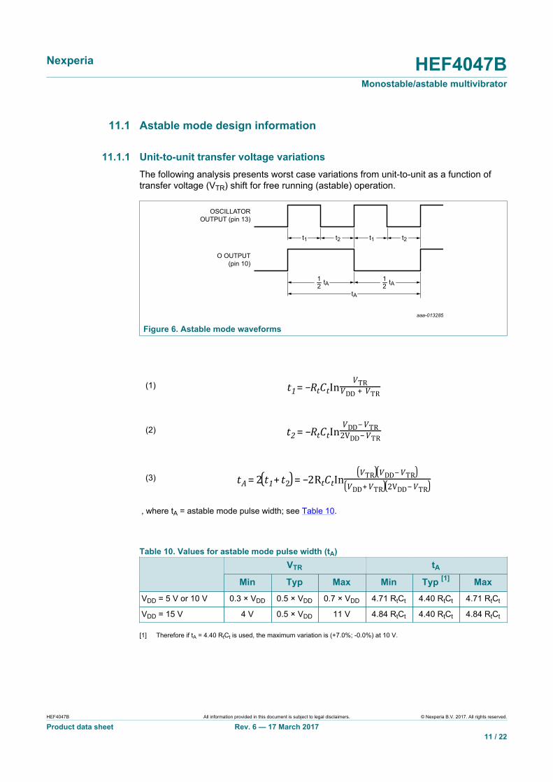
11.1 Astable mode design information
11.1.1 Unit-to-unit transfer voltage variationsThe following analysis presents worst case variations from unit-to-unit as a function oftransfer voltage (VTR) shift for free running (astable) operation.
aaa-013285
OSCILLATOROUTPUT (pin 13)
O OUTPUT(pin 10)
t1 t2 t2
tA
tA
t1
12 tA
12
Figure 6. Astable mode waveforms
(1)
(2)
(3)
, where tA = astable mode pulse width; see Table 10.
Table 10. Values for astable mode pulse width (tA)VTR tA
Min Typ Max Min Typ [1] MaxVDD = 5 V or 10 V 0.3 × VDD 0.5 × VDD 0.7 × VDD 4.71 RtCt 4.40 RtCt 4.71 RtCt
VDD = 15 V 4 V 0.5 × VDD 11 V 4.84 RtCt 4.40 RtCt 4.84 RtCt
[1] Therefore if tA = 4.40 RtCt is used, the maximum variation is (+7.0%; -0.0%) at 10 V.

Nexperia HEF4047BMonostable/astable multivibrator
HEF4047B All information provided in this document is subject to legal disclaimers. © Nexperia B.V. 2017. All rights reserved.
Product data sheet Rev. 6 — 17 March 201712 / 22
11.1.2 Variations due to changes in VDD
In addition to variations from unit-to-unit, the astable period may vary as a function offrequency with respect to VDD. Typical variations are presented graphically in Figure 7and Figure 8 with 10 V as a reference.
VDD (V)0 15105
aaa-013286
2.5
0
5.0
7.5
-2.5
period accuracyfor O and O
(%)
(1)(2)(3)
(1)Tamb = 25 °C; fo = 10 kHz; Ct = 100 pF; Rt = 220 kΩ.(2)Tamb = 25 °C; fo = 5 kHz; Ct = 100 pF; Rt = 470 kΩ.(3)Tamb = 25 °C; fo = 1 kHz; Ct = 1000 pF; Rt = 220 kΩ.Figure 7. Typical O and O period accuracy as a function of supply voltage; astable mode.
VDD (V)0 15105
aaa-013287
5
0
10
15
-5
period accuracyfor O and O
(%)
(1)(2)(3)(4)
(1)Tamb = 25 °C; fo = 500 kHz; Ct = 10 pF; Rt = 47 kΩ.(2)Tamb = 25 °C; fo = 225 kHz; Ct = 100 pF; Rt = 10 kΩ.(3)Tamb = 25 °C; fo = 100 kHz; Ct = 100 pF; Rt = 22 kΩ.(4)Tamb = 25 °C; fo = 50 kHz; Ct = 100 pF; Rt = 47 kΩ.Figure 8. Typical O and O period accuracy as a function of supply voltage; astable mode.
Nexperia HEF4047BMonostable/astable multivibrator
HEF4047B All information provided in this document is subject to legal disclaimers. © Nexperia B.V. 2017. All rights reserved.
Product data sheet Rev. 6 — 17 March 201713 / 22
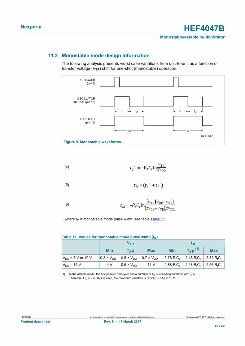
11.2 Monostable mode design informationThe following analysis presents worst case variations from unit-to-unit as a function oftransfer voltage (VTR) shift for one-shot (monostable) operation.
aaa-013288
+ TRIGGER(pin 8)
OSCILLATOROUTPUT (pin 13)
O OUTPUT(pin 10)
t1' t2
tM tM
t1' t2
Figure 9. Monostable waveforms.
(4)
(5)
(6)
, where tM = monostable mode pulse width; see table Table 11.
Table 11. Values for monostable mode pulse width (tM)VTR tM
Min Typ Max Min Typ [1] MaxVDD = 5 V or 10 V 0.3 × VDD 0.5 × VDD 0.7 × VDD 2.78 RtCt 2.48 RtCt 2.52 RtCt
VDD = 15 V 4 V 0.5 × VDD 11 V 2.88 RtCt 2.48 RtCt 2.56 RtCt
[1] In the astable mode, the first positive half cycle has a duration of tM: succeeding durations are 1⁄2 tA.Therefore if tM = 2.48 RtCt is used, the maximum variation is (+12%; -0.0%) at 10 V.

Nexperia HEF4047BMonostable/astable multivibrator
HEF4047B All information provided in this document is subject to legal disclaimers. © Nexperia B.V. 2017. All rights reserved.
Product data sheet Rev. 6 — 17 March 201714 / 22
11.2.1 Retrigger mode operationThe HEF4047B can be used in the retrigger mode to extend the output pulse duration.It can also be used to compare the frequency of an input signal with the frequency ofthe internal oscillator. In the retrigger mode, the input pulse is applied to pins 8 and 12,and the output is taken from pin 10 or 11. Normal monostable action is obtained whenone retrigger pulse is applied (see Figure 10). Extended pulse duration is obtained whenmore than one pulse is applied. For two input pulses, tRE = t1' + t1 + 2t2 . For more thantwo pulses, tRE (output O), terminates at some variable time, tD, after the termination ofthe last retrigger pulse. tD is variable because tRE (output O) terminates after the secondpositive edge of the oscillator output appears at flip-flop 4.
aaa-013289
OSCILLATOROUTPUT (pin 13)
+ TRIGGER;RETRIGGER
(pins 8, 12)
O OUTPUT(pin 10)
t2t1'
t1'
tRE
tRE tRE
t1t2
t2
tD
Figure 10. Retrigger mode waveforms.
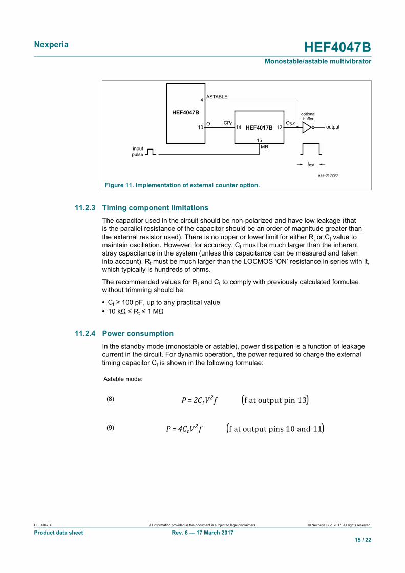
11.2.2 External counter optionThe use of external counting circuitry extends time tM by any amount. Advantagesinclude digitally controlled pulse duration, small timing capacitors for long time periods,and extremely fast recovery time. A typical implementation is shown in Figure 11.
The pulse duration at the output is:
(7)
Where text = pulse duration of the circuitry, and N is the number of counts used.
Nexperia HEF4047BMonostable/astable multivibrator
HEF4047B All information provided in this document is subject to legal disclaimers. © Nexperia B.V. 2017. All rights reserved.
Product data sheet Rev. 6 — 17 March 201715 / 22
aaa-013290
HEF4047B
HEF4017B
ASTABLE
inputpulse
4
output
text
optionalbuffer
10 14CP0
MR
12O5-9
15
O
Figure 11. Implementation of external counter option.
11.2.3 Timing component limitationsThe capacitor used in the circuit should be non-polarized and have low leakage (thatis the parallel resistance of the capacitor should be an order of magnitude greater thanthe external resistor used). There is no upper or lower limit for either Rt or Ct value tomaintain oscillation. However, for accuracy, Ct must be much larger than the inherentstray capacitance in the system (unless this capacitance can be measured and takeninto account). Rt must be much larger than the LOCMOS ‘ON’ resistance in series with it,which typically is hundreds of ohms.
The recommended values for Rt and Ct to comply with previously calculated formulaewithout trimming should be:
• Ct ≥ 100 pF, up to any practical value• 10 kΩ ≤ Rt ≤ 1 MΩ
11.2.4 Power consumptionIn the standby mode (monostable or astable), power dissipation is a function of leakagecurrent in the circuit. For dynamic operation, the power required to charge the externaltiming capacitor Ct is shown in the following formulae:
Astable mode:
(8)
(9)

Nexperia HEF4047BMonostable/astable multivibrator
HEF4047B All information provided in this document is subject to legal disclaimers. © Nexperia B.V. 2017. All rights reserved.
Product data sheet Rev. 6 — 17 March 201716 / 22
Monostable mode:
(10)
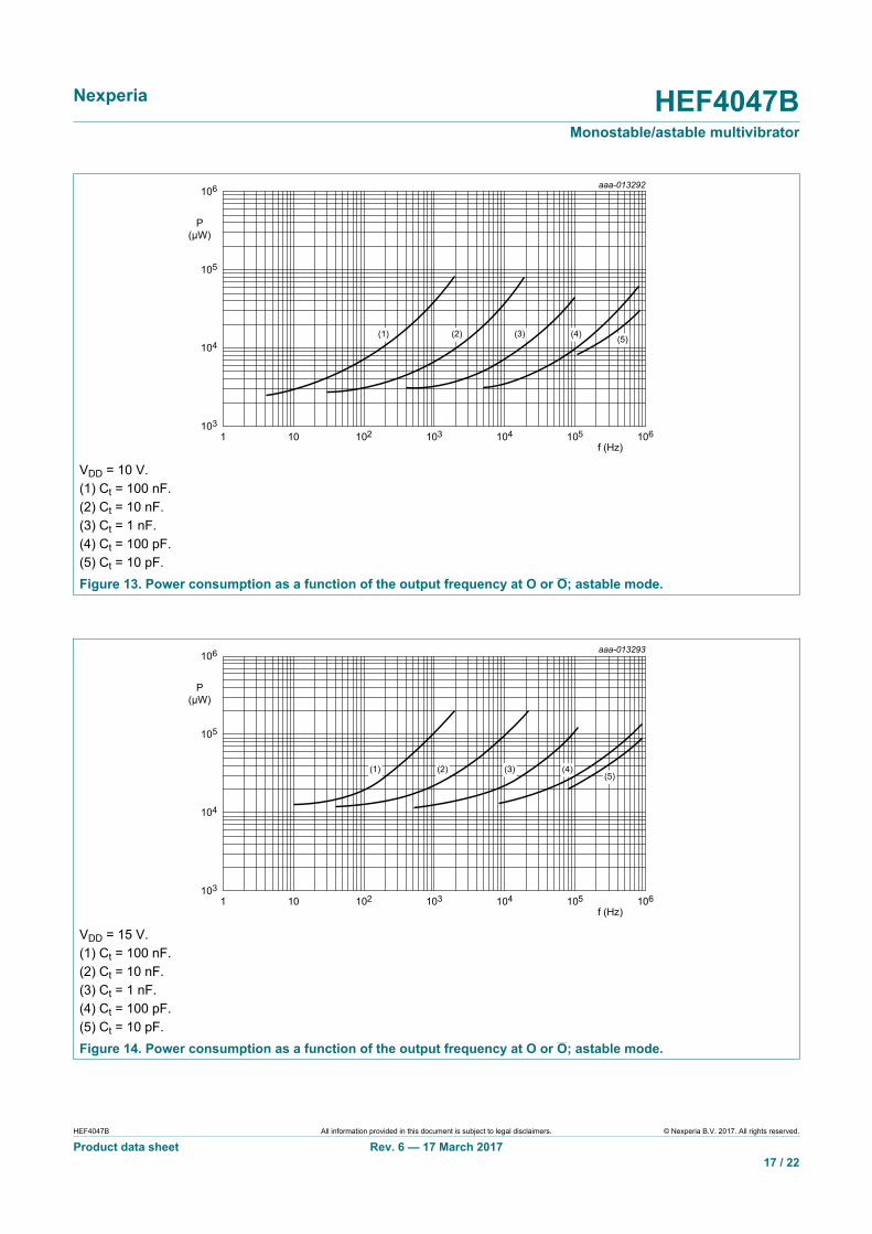
Because the power dissipation does not depend on Rt, a design for minimum powerdissipation would be a small value of Ct. The value of R would depend on the desiredperiod (within the limitations discussed previously). Typical power consumption in astablemode is shown in Figure 12, Figure 13 and Figure 14.
aaa-013291
103
102
104
105
P(µW)
10
f (Hz)1 10610510410 103102
(1) (2) (3) (4) (5)
VDD = 5 V.(1) Ct = 100 nF.(2) Ct = 10 nF.(3) Ct = 1 nF.(4) Ct = 100 pF.(5) Ct = 10 pF.Figure 12. Power consumption as a function of the output frequency at O or O; astable mode.
Nexperia HEF4047BMonostable/astable multivibrator
HEF4047B All information provided in this document is subject to legal disclaimers. © Nexperia B.V. 2017. All rights reserved.
Product data sheet Rev. 6 — 17 March 201717 / 22
aaa-013292
f (Hz)1 105 10610410310 102
105
104
106
P(µW)
103
(1) (2) (3) (4) (5)
VDD = 10 V.(1) Ct = 100 nF.(2) Ct = 10 nF.(3) Ct = 1 nF.(4) Ct = 100 pF.(5) Ct = 10 pF.Figure 13. Power consumption as a function of the output frequency at O or O; astable mode.
aaa-013293
f (Hz)1 105 10610410310 102
105
104
106
P(µW)
103
(1) (2) (3) (4)(5)
VDD = 15 V.(1) Ct = 100 nF.(2) Ct = 10 nF.(3) Ct = 1 nF.(4) Ct = 100 pF.(5) Ct = 10 pF.Figure 14. Power consumption as a function of the output frequency at O or O; astable mode.

Nexperia HEF4047BMonostable/astable multivibrator
HEF4047B All information provided in this document is subject to legal disclaimers. © Nexperia B.V. 2017. All rights reserved.
Product data sheet Rev. 6 — 17 March 201718 / 22
12 Package outline
UNIT Amax. A1 A2 A3 bp c D(1) E(1) (1)e HE L Lp Q Zywv θ
REFERENCESOUTLINEVERSION
EUROPEANPROJECTION ISSUE DATE
IEC JEDEC JEITA
mm
inches
1.75 0.250.10
1.451.25 0.25 0.49
0.360.250.19
8.758.55
4.03.8 1.27 6.2
5.80.70.6
0.70.3 8
0
oo
0.25 0.1
DIMENSIONS (inch dimensions are derived from the original mm dimensions)
Note1. Plastic or metal protrusions of 0.15 mm (0.006 inch) maximum per side are not included.
1.00.4
SOT108-1
X
w M
θ
AA1A2
bp
D
HE
Lp
Q
detail X
E
Z
e
c
L
v M A
(A )3
A
7
8
1
14
y
076E06 MS-012
pin 1 index
0.069 0.0100.004
0.0570.049 0.01 0.019
0.0140.01000.0075
0.350.34
0.160.15 0.05
1.05
0.0410.2440.228
0.0280.024
0.0280.0120.01
0.25
0.01 0.0040.0390.016
99-12-2703-02-19
0 2.5 5 mm
scale
SO14: plastic small outline package; 14 leads; body width 3.9 mm SOT108-1
Figure 15. Package outline SOT108-1 (SO14)
Nexperia HEF4047BMonostable/astable multivibrator
HEF4047B All information provided in this document is subject to legal disclaimers. © Nexperia B.V. 2017. All rights reserved.
Product data sheet Rev. 6 — 17 March 201719 / 22
13 AbbreviationsTable 12. AbbreviationsAcronym DescriptionDUT Device Under Test
14 Revision historyTable 13. Revision historyDocument ID Release date Data sheet status Change notice SupersedesHEF4047B v.6 20170317 Product data sheet - HEF4047B v.5
Modifications: • The format of this data sheet has been redesigned to comply with the new identity guidelinesof Nexperia.
• Legal texts have been adapted to the new company name where appropriate.
HEF4047B v.5 20151216 Product data sheet - HEF4047B v.4
Modifications: • Type number HEF4047BP (SOT27-1) removed.
HEF4047B v.4 20140915 Product data sheet - HEF4047B_CVN_3
Modifications: • The format of this data sheet has been redesigned to comply with the new identityguidelines of NXP Semiconductors.
• Legal texts have been adapted to the new company name where appropriate.
HEF4047B_CVN_3 19950101 Product specification - -
Nexperia HEF4047BMonostable/astable multivibrator
HEF4047B All information provided in this document is subject to legal disclaimers. © Nexperia B.V. 2017. All rights reserved.
Product data sheet Rev. 6 — 17 March 201720 / 22
15 Legal information
15.1 Data sheet status
Document status[1][2] Product status[3] Definition
Objective [short] data sheet Development This document contains data from the objective specification for productdevelopment.
Preliminary [short] data sheet Qualification This document contains data from the preliminary specification.
Product [short] data sheet Production This document contains the product specification.
[1] Please consult the most recently issued document before initiating or completing a design.[2] The term 'short data sheet' is explained in section "Definitions".[3] The product status of device(s) described in this document may have changed since this document was published and may differ in case of multiple
devices. The latest product status information is available on the Internet at URL http://www.nexperia.com.
15.2 DefinitionsDraft — The document is a draft version only. The content is still underinternal review and subject to formal approval, which may result inmodifications or additions. Nexperia does not give any representations orwarranties as to the accuracy or completeness of information included hereinand shall have no liability for the consequences of use of such information.
Short data sheet — A short data sheet is an extract from a full data sheetwith the same product type number(s) and title. A short data sheet isintended for quick reference only and should not be relied upon to containdetailed and full information. For detailed and full information see therelevant full data sheet, which is available on request via the local Nexperiasales office. In case of any inconsistency or conflict with the short data sheet,the full data sheet shall prevail.
Product specification — The information and data provided in a Productdata sheet shall define the specification of the product as agreed betweenNexperia and its customer, unless Nexperia and customer have explicitlyagreed otherwise in writing. In no event however, shall an agreement bevalid in which the Nexperia product is deemed to offer functions and qualitiesbeyond those described in the Product data sheet.
15.3 DisclaimersLimited warranty and liability — Information in this document is believedto be accurate and reliable. However, Nexperia does not give anyrepresentations or warranties, expressed or implied, as to the accuracyor completeness of such information and shall have no liability for theconsequences of use of such information. Nexperia takes no responsibilityfor the content in this document if provided by an information source outsideof Nexperia. In no event shall Nexperia be liable for any indirect, incidental,punitive, special or consequential damages (including - without limitation -lost profits, lost savings, business interruption, costs related to the removalor replacement of any products or rework charges) whether or not suchdamages are based on tort (including negligence), warranty, breach ofcontract or any other legal theory. Notwithstanding any damages thatcustomer might incur for any reason whatsoever, Nexperia's aggregate andcumulative liability towards customer for the products described herein shallbe limited in accordance with the Terms and conditions of commercial sale ofNexperia.
Right to make changes — Nexperia reserves the right to make changesto information published in this document, including without limitationspecifications and product descriptions, at any time and without notice. Thisdocument supersedes and replaces all information supplied prior to thepublication hereof.
Suitability for use — Nexperia products are not designed, authorized orwarranted to be suitable for use in life support, life-critical or safety-critical
systems or equipment, nor in applications where failure or malfunctionof an Nexperia product can reasonably be expected to result in personalinjury, death or severe property or environmental damage. Nexperia and itssuppliers accept no liability for inclusion and/or use of Nexperia products insuch equipment or applications and therefore such inclusion and/or use is atthe customer’s own risk.
Applications — Applications that are described herein for any of theseproducts are for illustrative purposes only. Nexperia makes no representationor warranty that such applications will be suitable for the specified usewithout further testing or modification. Customers are responsible for thedesign and operation of their applications and products using Nexperiaproducts, and Nexperia accepts no liability for any assistance withapplications or customer product design. It is customer’s sole responsibilityto determine whether the Nexperia product is suitable and fit for thecustomer’s applications and products planned, as well as for the plannedapplication and use of customer’s third party customer(s). Customers shouldprovide appropriate design and operating safeguards to minimize the risksassociated with their applications and products. Nexperia does not acceptany liability related to any default, damage, costs or problem which is basedon any weakness or default in the customer’s applications or products, orthe application or use by customer’s third party customer(s). Customer isresponsible for doing all necessary testing for the customer’s applicationsand products using Nexperia products in order to avoid a default of theapplications and the products or of the application or use by customer’s thirdparty customer(s). Nexperia does not accept any liability in this respect.
Limiting values — Stress above one or more limiting values (as defined inthe Absolute Maximum Ratings System of IEC 60134) will cause permanentdamage to the device. Limiting values are stress ratings only and (proper)operation of the device at these or any other conditions above thosegiven in the Recommended operating conditions section (if present) or theCharacteristics sections of this document is not warranted. Constant orrepeated exposure to limiting values will permanently and irreversibly affectthe quality and reliability of the device.
Terms and conditions of commercial sale — Nexperia products aresold subject to the general terms and conditions of commercial sale, aspublished at http://www.nexperia.com/profile/terms, unless otherwise agreedin a valid written individual agreement. In case an individual agreement isconcluded only the terms and conditions of the respective agreement shallapply. Nexperia hereby expressly objects to applying the customer’s generalterms and conditions with regard to the purchase of Nexperia products bycustomer.
No offer to sell or license — Nothing in this document may be interpretedor construed as an offer to sell products that is open for acceptance orthe grant, conveyance or implication of any license under any copyrights,patents or other industrial or intellectual property rights.
Export control — This document as well as the item(s) described hereinmay be subject to export control regulations. Export might require a priorauthorization from competent authorities.
Nexperia HEF4047BMonostable/astable multivibrator
HEF4047B All information provided in this document is subject to legal disclaimers. © Nexperia B.V. 2017. All rights reserved.
Product data sheet Rev. 6 — 17 March 201721 / 22
Non-automotive qualified products — Unless this data sheet expresslystates that this specific Nexperia product is automotive qualified, theproduct is not suitable for automotive use. It is neither qualified nor tested inaccordance with automotive testing or application requirements. Nexperiaaccepts no liability for inclusion and/or use of non-automotive qualifiedproducts in automotive equipment or applications. In the event that customeruses the product for design-in and use in automotive applications toautomotive specifications and standards, customer (a) shall use the productwithout Nexperia's warranty of the product for such automotive applications,use and specifications, and (b) whenever customer uses the product forautomotive applications beyond Nexperia's specifications such use shall besolely at customer’s own risk, and (c) customer fully indemnifies Nexperiafor any liability, damages or failed product claims resulting from customer
design and use of the product for automotive applications beyond Nexperia'sstandard warranty and Nexperia's product specifications.
Translations — A non-English (translated) version of a document is forreference only. The English version shall prevail in case of any discrepancybetween the translated and English versions.
15.4 TrademarksNotice: All referenced brands, product names, service names andtrademarks are the property of their respective owners.
Nexperia HEF4047BMonostable/astable multivibrator
Please be aware that important notices concerning this document and the product(s)described herein, have been included in section 'Legal information'.
© Nexperia B.V. 2017. All rights reserved.For more information, please visit: http://www.nexperia.comFor sales office addresses, please send an email to: [email protected]
Date of release: 17 March 2017Document identifier: HEF4047B
Contents1 General description ............................................ 12 Features and benefits .........................................12.1 General .............................................................. 12.2 Monostable multivibrator ....................................12.3 Astable multivibrator .......................................... 13 Ordering information .......................................... 14 Functional diagram ............................................. 25 Pinning information ............................................ 35.1 Pinning ...............................................................35.2 Pin description ................................................... 36 Functional description ........................................47 Limiting values ....................................................58 Recommended operating conditions ................ 59 Static characteristics .......................................... 610 Dynamic characteristics .....................................710.1 Waveform and test circuit ..................................811 Application information ....................................1011.1 Astable mode design information .................... 1111.1.1 Unit-to-unit transfer voltage variations ............. 1111.1.2 Variations due to changes in VDD ...................1211.2 Monostable mode design information ..............1311.2.1 Retrigger mode operation ................................1411.2.2 External counter option ....................................1411.2.3 Timing component limitations .......................... 1511.2.4 Power consumption ......................................... 1512 Package outline .................................................1813 Abbreviations .................................................... 1914 Revision history ................................................ 1915 Legal information ..............................................20
Mouser Electronics
Authorized Distributor
Click to View Pricing, Inventory, Delivery & Lifecycle Information: Nexperia:
HEF4047BT,652 HEF4047BT,653
Related Documents