I 2313 Monolithic Active Pixel Sensors With In-Pixel Double Sampling Operation and Column-Level Discrimination Grzegorz Deptuch, Member, IEEE, Gilles Claus, Claude Colledani, Yavuz De˘ gerli, Member, IEEE, Wojciech Dulinski, Nicolas Fourches, Member, IEEE, Goetz Gaycken, Damien Grandjean, Abdelkader Himmi, Christine Hu-Guo, Pierre Lutz, Michel Rouger, Isabelle Valin, and Marc Winter Abstract—Monolithic active pixel sensors constitute a viable alternative to hybrid pixel sensors and charge coupled devices for the next generation of vertex detectors. Possible applications will strongly depend on a successful implementation of on-chip hit recognition and sparsification schemes. The task is tough, first because of very small signal amplitudes ( mV), which are of the same order of magnitude as natural dispersions in the transistor threshold voltages, secondly because of the limitation to use only one type of transistor over the sensitive area. This paper presents a 30 128 pixel prototype chip, featuring fast, column parallel signal processing. The pixel concept combines in-pixel amplification with double sampling operation. The pixel output is a differential current signal proportional to the difference between the reference level and the charge collected. The readout of the pixel is two-phase, matching discrimination circuitry im- plemented at the end of each column. Low-noise discriminators feature autozero functionality. The details of the chip design are presented. Difficulties, encoun- tered in the first attempt to address on-line hit recognition, are re- ported. Performances of the pixel and discriminator blocks, deter- mined in separate measurements, are discussed. An important part of this paper consists of results of first tests performed with soft X-rays from a Fe source. Index Terms—APS, CMOS APS, double sampling, image sen- sors, particle detector, pixel detectors, system-on-chip. I. INTRODUCTION B ECAUSE of physics requirements, the need of precise vertex measurements makes a high-resolution vertex detector (VXD) an essential part of the experiment appa- ratus. One of the options considered for VXD construction in a future linear collider is a monolithic active pixel sensors (MAPS)-based detector. The ability of MAPS realized in a Manuscript received November 13, 2003; revised June 3, 2004. G. Deptuch is with LEPSI, 67037 Strasbourg Cedex 02, France (e-mail: [email protected]) on leave from UST AGH, 30-059 Krakow, Poland. G. Claus, C. Colledani, and W. Dulinski are with LEPSI, 67037 Strasbourg Cedex 02, France (e-mail: [email protected]; [email protected]; [email protected]). Y. De˘ gerli, N. Fourches, P. Lutz, and M. Rouger are with CEA Saclay, DAPNIA/SEDI and SPP, 91191 Gif-sur-Yvette Cedex, France (e-mail: [email protected]; [email protected]; [email protected]; [email protected]). G. Gaycken, D. Grandjean, A. Himmi, C. Hu-Guo, I. Valin, and M. Winter are with IReS, CNRS-IN2P3/ULP, 67037 Strasbourg Cedex 02, France (e-mail: [email protected]; [email protected]; [email protected]; [email protected]; [email protected]; [email protected]). Digital Object Identifier 10.1109/TNS.2004.835551 CMOS process, to provide charged particle tracking has been demonstrated with the Minimum Ionising Particle Mos Active Pixel Sensor (MIMOSA) chips family (see, e.g., [1]. The results were obtained on a series of small scale and 1 million pixel large prototypes that were designed exploiting a classical three-transistor (3T) pixel configuration. The use of MAPS in particle physics [2] will strongly depend on a successful implementation of an on-chip hit recognition and sparsification scheme. This is not a trivial task, because of very small signal amplitudes, in the range of millivolts, which are of the same order of magnitude as transistor threshold vari- ations of a CMOS process. The solution consisting in storing of reference values for each pixel is impracticable, because of waste of active area due to the large memory required. There- fore, the correction for offset, performed during every access to the pixel, has been adopted. The offset correction, called calibra- tion, consists in reading empty data from the analog readout, in- cluding the pixel circuitry, chain with a short-circuited input. A new column-based, low power, offset compensated (autozeroed) multistage comparator has been developed completing the pixel design [3]. A planned final detector would include an array of identical pixels with their addressing, signal processing within the chip, sparsification, and data transmission circuits. The de- sign of the MIMOSA VI chip, focusing the interest of this paper, is a first step toward construction of high performance detection system integrated on chip. Additionally, the fabrication goal of the MIMOSA VI chip was to test the possibility of the in-pixel sampling and storing signals from two different time slots. This could be the first step for further extension of the number of memory cells aiming at multiple and fast signal sampling during the train time in the collider. II. PIXEL DESIGN Novel ideas, optimizing charge sensitive elements (CSEs) for a vertex detector environment and new pixel configurations with signal amplification and double sampling operation, have been recently proposed [4]. In this new CSE, the charge gen- erated in the lightly doped, undepleted volume is collected by the n-well/p-epi (n-well/p-sub) diode, as it was proposed for 100% fill factor devices in visible light applications [5]. The reverse bias is provided in a continuous way via a diode. This one is forward biased with a leakage current of

Welcome message from author
This document is posted to help you gain knowledge. Please leave a comment to let me know what you think about it! Share it to your friends and learn new things together.
Transcript
I 2313
Monolithic Active Pixel Sensors WithIn-Pixel Double Sampling Operation
and Column-Level DiscriminationGrzegorz Deptuch, Member, IEEE, Gilles Claus, Claude Colledani, Yavuz Degerli, Member, IEEE, Wojciech Dulinski,
Nicolas Fourches, Member, IEEE, Goetz Gaycken, Damien Grandjean, Abdelkader Himmi, Christine Hu-Guo,Pierre Lutz, Michel Rouger, Isabelle Valin, and Marc Winter
Abstract—Monolithic active pixel sensors constitute a viablealternative to hybrid pixel sensors and charge coupled devicesfor the next generation of vertex detectors. Possible applicationswill strongly depend on a successful implementation of on-chiphit recognition and sparsification schemes. The task is tough,first because of very small signal amplitudes ( mV), which areof the same order of magnitude as natural dispersions in thetransistor threshold voltages, secondly because of the limitation touse only one type of transistor over the sensitive area. This paperpresents a 30 128 pixel prototype chip, featuring fast, columnparallel signal processing. The pixel concept combines in-pixelamplification with double sampling operation. The pixel outputis a differential current signal proportional to the differencebetween the reference level and the charge collected. The readoutof the pixel is two-phase, matching discrimination circuitry im-plemented at the end of each column. Low-noise discriminatorsfeature autozero functionality.
The details of the chip design are presented. Difficulties, encoun-tered in the first attempt to address on-line hit recognition, are re-ported. Performances of the pixel and discriminator blocks, deter-mined in separate measurements, are discussed. An important partof this paper consists of results of first tests performed with softX-rays from a 55Fe source.
Index Terms—APS, CMOS APS, double sampling, image sen-sors, particle detector, pixel detectors, system-on-chip.
I. INTRODUCTION
B ECAUSE of physics requirements, the need of precisevertex measurements makes a high-resolution vertex
detector (VXD) an essential part of the experiment appa-ratus. One of the options considered for VXD constructionin a future linear collider is a monolithic active pixel sensors(MAPS)-based detector. The ability of MAPS realized in a
Manuscript received November 13, 2003; revised June 3, 2004.G. Deptuch is with LEPSI, 67037 Strasbourg Cedex 02, France (e-mail:
[email protected]) on leave from UST AGH, 30-059 Krakow, Poland.G. Claus, C. Colledani, and W. Dulinski are with LEPSI, 67037 Strasbourg
Cedex 02, France (e-mail: [email protected]; [email protected];[email protected]).
Y. Degerli, N. Fourches, P. Lutz, and M. Rouger are with CEASaclay, DAPNIA/SEDI and SPP, 91191 Gif-sur-Yvette Cedex, France(e-mail: [email protected]; [email protected];[email protected]; [email protected]).
G. Gaycken, D. Grandjean, A. Himmi, C. Hu-Guo, I. Valin, and M. Winterare with IReS, CNRS-IN2P3/ULP, 67037 Strasbourg Cedex 02, France(e-mail: [email protected]; [email protected];[email protected]; [email protected];[email protected]; [email protected]).
Digital Object Identifier 10.1109/TNS.2004.835551
CMOS process, to provide charged particle tracking has beendemonstrated with the Minimum Ionising Particle Mos ActivePixel Sensor (MIMOSA) chips family (see, e.g., [1]. Theresults were obtained on a series of small scale and 1 millionpixel large prototypes that were designed exploiting a classicalthree-transistor (3T) pixel configuration.
The use of MAPS in particle physics [2] will strongly dependon a successful implementation of an on-chip hit recognitionand sparsification scheme. This is not a trivial task, because ofvery small signal amplitudes, in the range of millivolts, whichare of the same order of magnitude as transistor threshold vari-ations of a CMOS process. The solution consisting in storingof reference values for each pixel is impracticable, because ofwaste of active area due to the large memory required. There-fore, the correction for offset, performed during every access tothe pixel, has been adopted. The offset correction, called calibra-tion, consists in reading empty data from the analog readout, in-cluding the pixel circuitry, chain with a short-circuited input. Anew column-based, low power, offset compensated (autozeroed)multistage comparator has been developed completing the pixeldesign [3]. A planned final detector would include an array ofidentical pixels with their addressing, signal processing withinthe chip, sparsification, and data transmission circuits. The de-sign of the MIMOSA VI chip, focusing the interest of this paper,is a first step toward construction of high performance detectionsystem integrated on chip. Additionally, the fabrication goal ofthe MIMOSA VI chip was to test the possibility of the in-pixelsampling and storing signals from two different time slots. Thiscould be the first step for further extension of the number ofmemory cells aiming at multiple and fast signal sampling duringthe train time in the collider.
II. PIXEL DESIGN
Novel ideas, optimizing charge sensitive elements (CSEs)for a vertex detector environment and new pixel configurationswith signal amplification and double sampling operation, havebeen recently proposed [4]. In this new CSE, the charge gen-erated in the lightly doped, undepleted volume is collected bythe n-well/p-epi (n-well/p-sub) diode, as it was proposed for100% fill factor devices in visible light applications [5]. Thereverse bias is provided in a continuous way via adiode. This one is forward biased with a leakage current of
2314
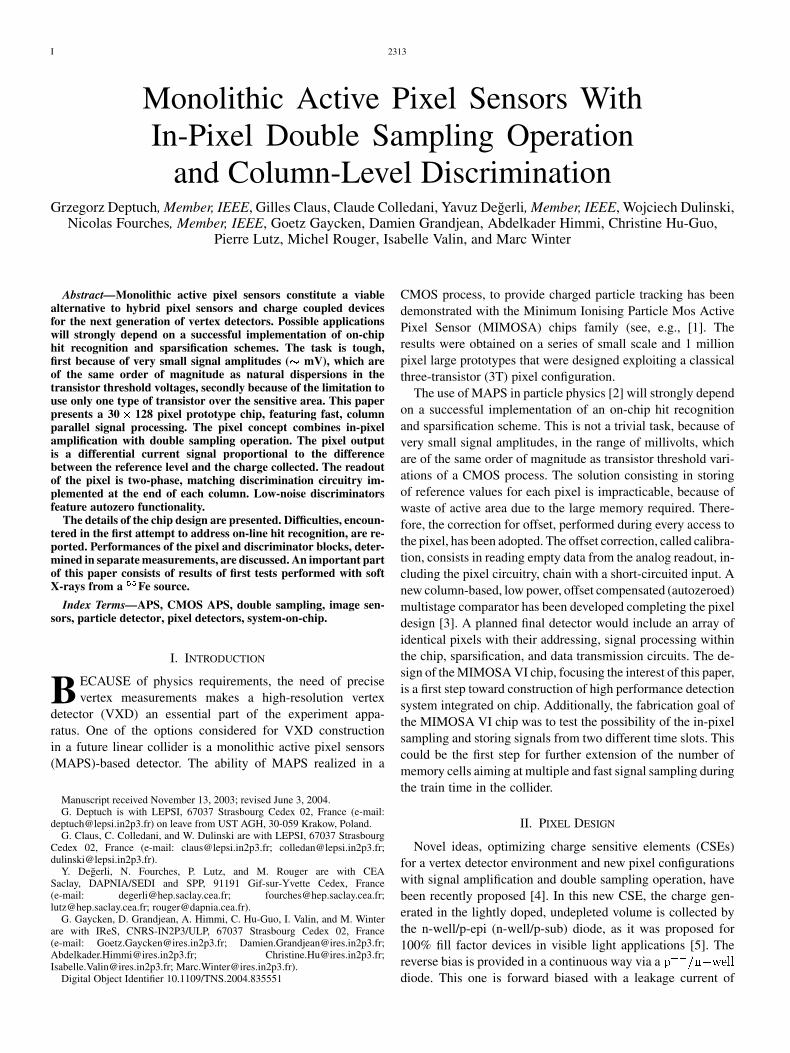
Fig. 1. MIMOSA VI pixel concept based on autoreverse polarization of charge collecting diode, where SF, VA, and LT stand for source follower, voltage amplifier,and linearized transconductance pair, respectively, and the column level circuitry includes signal discrimination and multiplexing of resulting signals.
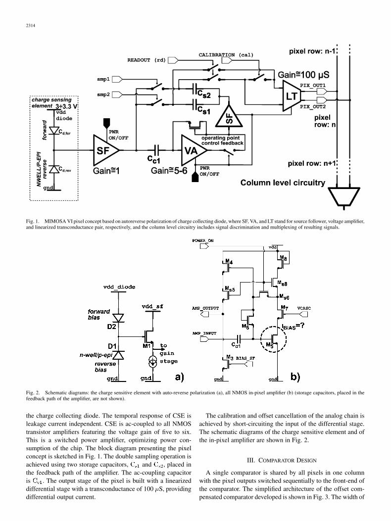
Fig. 2. Schematic diagrams: the charge sensitive element with auto-reverse polarization (a), all NMOS in-pixel amplifier (b) (storage capacitors, placed in thefeedback path of the amplifier, are not shown).
the charge collecting diode. The temporal response of CSE isleakage current independent. CSE is ac-coupled to all NMOStransistor amplifiers featuring the voltage gain of five to six.This is a switched power amplifier, optimizing power con-sumption of the chip. The block diagram presenting the pixelconcept is sketched in Fig. 1. The double sampling operation isachieved using two storage capacitors, and , placed inthe feedback path of the amplifier. The ac-coupling capacitoris . The output stage of the pixel is built with a linearizeddifferential stage with a transconductance of 100 S, providingdifferential output current.
The calibration and offset cancellation of the analog chain isachieved by short-circuiting the input of the differential stage.The schematic diagrams of the charge sensitive element and ofthe in-pixel amplifier are shown in Fig. 2.
III. COMPARATOR DESIGN
A single comparator is shared by all pixels in one columnwith the pixel outputs switched sequentially to the front-end ofthe comparator. The simplified architecture of the offset com-pensated comparator developed is shown in Fig. 3. The width of
2315
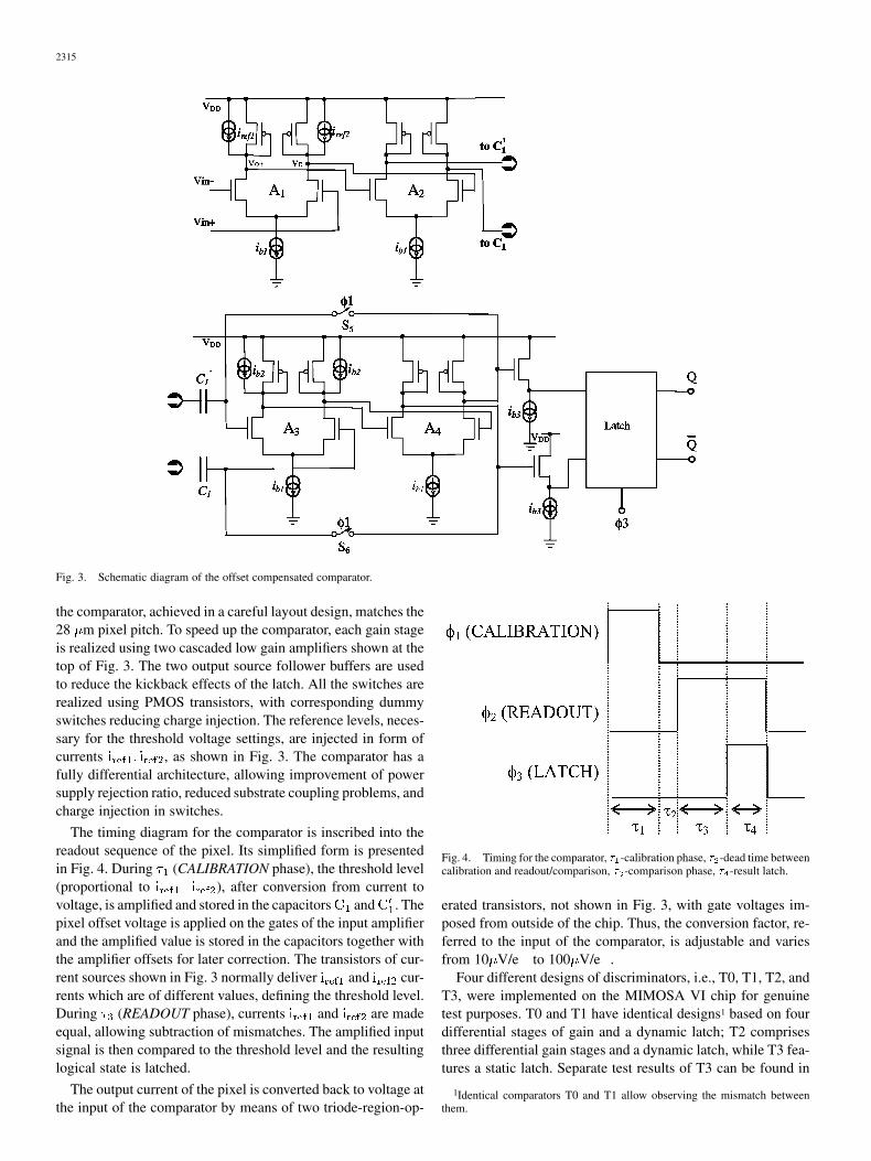
Fig. 3. Schematic diagram of the offset compensated comparator.
the comparator, achieved in a careful layout design, matches the28 m pixel pitch. To speed up the comparator, each gain stageis realized using two cascaded low gain amplifiers shown at thetop of Fig. 3. The two output source follower buffers are usedto reduce the kickback effects of the latch. All the switches arerealized using PMOS transistors, with corresponding dummyswitches reducing charge injection. The reference levels, neces-sary for the threshold voltage settings, are injected in form ofcurrents , as shown in Fig. 3. The comparator has afully differential architecture, allowing improvement of powersupply rejection ratio, reduced substrate coupling problems, andcharge injection in switches.
The timing diagram for the comparator is inscribed into thereadout sequence of the pixel. Its simplified form is presentedin Fig. 4. During (CALIBRATION phase), the threshold level(proportional to ), after conversion from current tovoltage, is amplified and stored in the capacitors and . Thepixel offset voltage is applied on the gates of the input amplifierand the amplified value is stored in the capacitors together withthe amplifier offsets for later correction. The transistors of cur-rent sources shown in Fig. 3 normally deliver and cur-rents which are of different values, defining the threshold level.During (READOUT phase), currents and are madeequal, allowing subtraction of mismatches. The amplified inputsignal is then compared to the threshold level and the resultinglogical state is latched.
The output current of the pixel is converted back to voltage atthe input of the comparator by means of two triode-region-op-
Fig. 4. Timing for the comparator, � -calibration phase, � -dead time betweencalibration and readout/comparison, � -comparison phase, � -result latch.
erated transistors, not shown in Fig. 3, with gate voltages im-posed from outside of the chip. Thus, the conversion factor, re-ferred to the input of the comparator, is adjustable and variesfrom 10 V/e to 100 V/e .
Four different designs of discriminators, i.e., T0, T1, T2, andT3, were implemented on the MIMOSA VI chip for genuinetest purposes. T0 and T1 have identical designs1 based on fourdifferential stages of gain and a dynamic latch; T2 comprisesthree differential gain stages and a dynamic latch, while T3 fea-tures a static latch. Separate test results of T3 can be found in
1Identical comparators T0 and T1 allow observing the mismatch betweenthem.
2316 I
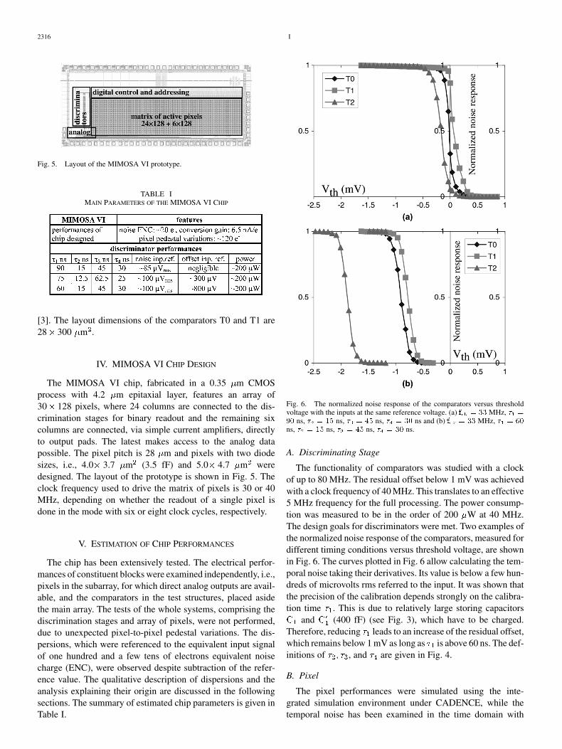
Fig. 5. Layout of the MIMOSA VI prototype.
TABLE IMAIN PARAMETERS OF THE MIMOSA VI CHIP
[3]. The layout dimensions of the comparators T0 and T1 are28 300 m .
IV. MIMOSA VI CHIP DESIGN
The MIMOSA VI chip, fabricated in a 0.35 m CMOSprocess with 4.2 m epitaxial layer, features an array of30 128 pixels, where 24 columns are connected to the dis-crimination stages for binary readout and the remaining sixcolumns are connected, via simple current amplifiers, directlyto output pads. The latest makes access to the analog datapossible. The pixel pitch is 28 m and pixels with two diodesizes, i.e., 4.0 3.7 m (3.5 fF) and 5.0 4.7 m weredesigned. The layout of the prototype is shown in Fig. 5. Theclock frequency used to drive the matrix of pixels is 30 or 40MHz, depending on whether the readout of a single pixel isdone in the mode with six or eight clock cycles, respectively.
V. ESTIMATION OF CHIP PERFORMANCES
The chip has been extensively tested. The electrical perfor-mances of constituent blocks were examined independently, i.e.,pixels in the subarray, for which direct analog outputs are avail-able, and the comparators in the test structures, placed asidethe main array. The tests of the whole systems, comprising thediscrimination stages and array of pixels, were not performed,due to unexpected pixel-to-pixel pedestal variations. The dis-persions, which were referenced to the equivalent input signalof one hundred and a few tens of electrons equivalent noisecharge (ENC), were observed despite subtraction of the refer-ence value. The qualitative description of dispersions and theanalysis explaining their origin are discussed in the followingsections. The summary of estimated chip parameters is given inTable I.
Fig. 6. The normalized noise response of the comparators versus thresholdvoltage with the inputs at the same reference voltage. (a) f = 33 MHz, � =
90 ns, � = 15 ns, � = 45 ns, � = 30 ns and (b) f = 33 MHz, � = 60
ns, � = 15 ns, � = 45 ns, � = 30 ns.
A. Discriminating Stage
The functionality of comparators was studied with a clockof up to 80 MHz. The residual offset below 1 mV was achievedwith a clock frequency of 40 MHz. This translates to an effective5 MHz frequency for the full processing. The power consump-tion was measured to be in the order of 200 W at 40 MHz.The design goals for discriminators were met. Two examples ofthe normalized noise response of the comparators, measured fordifferent timing conditions versus threshold voltage, are shownin Fig. 6. The curves plotted in Fig. 6 allow calculating the tem-poral noise taking their derivatives. Its value is below a few hun-dreds of microvolts rms referred to the input. It was shown thatthe precision of the calibration depends strongly on the calibra-tion time . This is due to relatively large storing capacitors
and (400 fF) (see Fig. 3), which have to be charged.Therefore, reducing leads to an increase of the residual offset,which remains below 1 mV as long as is above 60 ns. The def-initions of , and are given in Fig. 4.
B. Pixel
The pixel performances were simulated using the inte-grated simulation environment under CADENCE, while thetemporal noise has been examined in the time domain with
2317
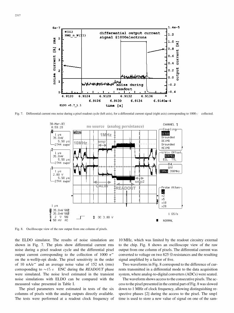
Fig. 7. Differential current rms noise during a pixel readout cycle (left axis), for a differential current signal (right axis) corresponding to 1000 e collected.
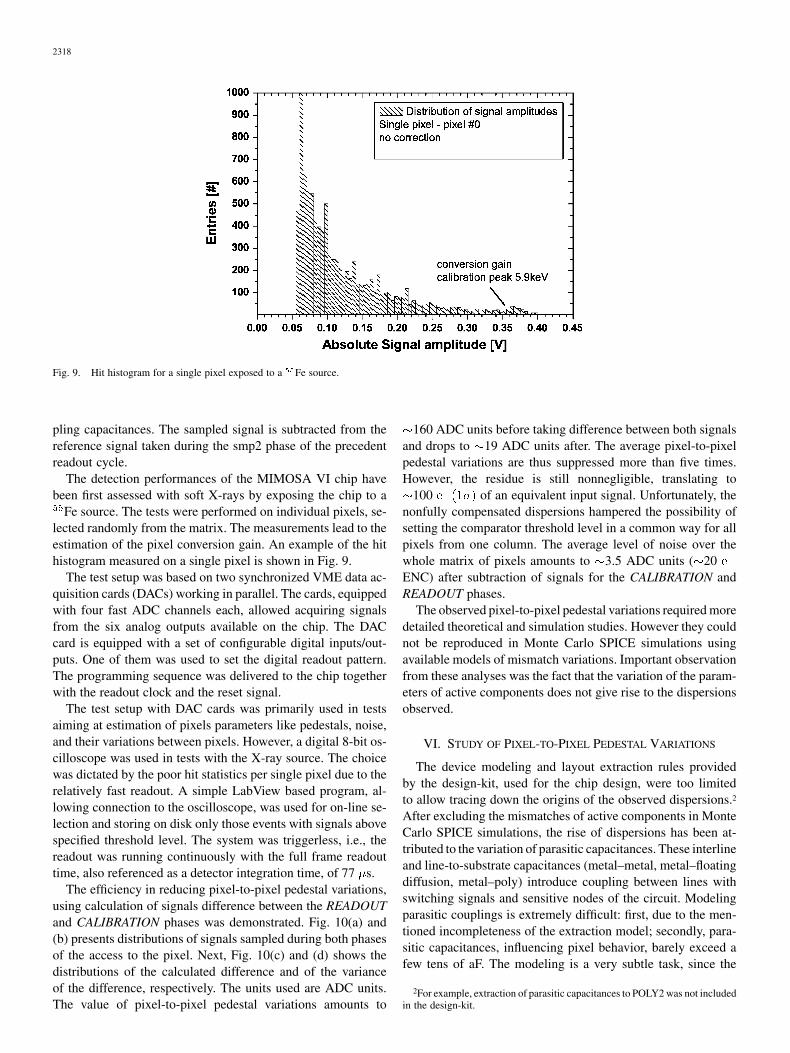
Fig. 8. Oscilloscope view of the raw output from one column of pixels.
the ELDO simulator. The results of noise simulation areshown in Fig. 7. The plots show differential current rmsnoise during a pixel readout cycle and the differential pixeloutput current corresponding to the collection of 1000on the n-well/p-epi diode. The pixel sensitivity in the orderof 10 nA/e and an average noise value of 152 nA (rms)corresponding to ENC during the READOUT phasewere simulated. The noise level estimated in the transientnoise simulations with ELDO can be compared with themeasured value presented in Table I.
The pixel parameters were estimated in tests of the sixcolumns of pixels with the analog outputs directly available.The tests were performed at a readout clock frequency of
10 MHz, which was limited by the readout circuitry externalto the chip. Fig. 8 shows an oscilloscope view of the rawoutput from one column of pixels. The differential current wasconverted to voltage on two 825 resistances and the resultingsignal amplified by a factor of five.
Two waveforms in Fig. 8 correspond to the difference of cur-rents transmitted in a differential mode to the data acquisitionsystem, where analog-to-digital converters (ADCs) were seated.
The waveform shows access to the consecutive pixels. The ac-cess to the pixel presented in the central part of Fig. 8 was sloweddown to 1 MHz of clock frequency, allowing distinguishing re-spective phases [2] during the access to the pixel. The smp1time is used to store a new value of signal on one of the sam-
2318
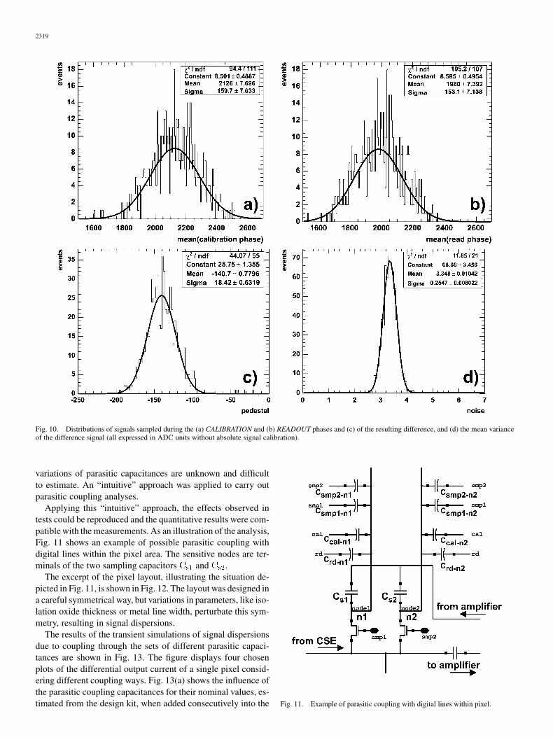
Fig. 9. Hit histogram for a single pixel exposed to a Fe source.
pling capacitances. The sampled signal is subtracted from thereference signal taken during the smp2 phase of the precedentreadout cycle.
The detection performances of the MIMOSA VI chip havebeen first assessed with soft X-rays by exposing the chip to a
Fe source. The tests were performed on individual pixels, se-lected randomly from the matrix. The measurements lead to theestimation of the pixel conversion gain. An example of the hithistogram measured on a single pixel is shown in Fig. 9.
The test setup was based on two synchronized VME data ac-quisition cards (DACs) working in parallel. The cards, equippedwith four fast ADC channels each, allowed acquiring signalsfrom the six analog outputs available on the chip. The DACcard is equipped with a set of configurable digital inputs/out-puts. One of them was used to set the digital readout pattern.The programming sequence was delivered to the chip togetherwith the readout clock and the reset signal.
The test setup with DAC cards was primarily used in testsaiming at estimation of pixels parameters like pedestals, noise,and their variations between pixels. However, a digital 8-bit os-cilloscope was used in tests with the X-ray source. The choicewas dictated by the poor hit statistics per single pixel due to therelatively fast readout. A simple LabView based program, al-lowing connection to the oscilloscope, was used for on-line se-lection and storing on disk only those events with signals abovespecified threshold level. The system was triggerless, i.e., thereadout was running continuously with the full frame readouttime, also referenced as a detector integration time, of 77 s.
The efficiency in reducing pixel-to-pixel pedestal variations,using calculation of signals difference between the READOUTand CALIBRATION phases was demonstrated. Fig. 10(a) and(b) presents distributions of signals sampled during both phasesof the access to the pixel. Next, Fig. 10(c) and (d) shows thedistributions of the calculated difference and of the varianceof the difference, respectively. The units used are ADC units.The value of pixel-to-pixel pedestal variations amounts to
160 ADC units before taking difference between both signalsand drops to 19 ADC units after. The average pixel-to-pixelpedestal variations are thus suppressed more than five times.However, the residue is still nonnegligible, translating to
100 of an equivalent input signal. Unfortunately, thenonfully compensated dispersions hampered the possibility ofsetting the comparator threshold level in a common way for allpixels from one column. The average level of noise over thewhole matrix of pixels amounts to 3.5 ADC units ( 20ENC) after subtraction of signals for the CALIBRATION andREADOUT phases.
The observed pixel-to-pixel pedestal variations required moredetailed theoretical and simulation studies. However they couldnot be reproduced in Monte Carlo SPICE simulations usingavailable models of mismatch variations. Important observationfrom these analyses was the fact that the variation of the param-eters of active components does not give rise to the dispersionsobserved.
VI. STUDY OF PIXEL-TO-PIXEL PEDESTAL VARIATIONS
The device modeling and layout extraction rules providedby the design-kit, used for the chip design, were too limitedto allow tracing down the origins of the observed dispersions.2
After excluding the mismatches of active components in MonteCarlo SPICE simulations, the rise of dispersions has been at-tributed to the variation of parasitic capacitances. These interlineand line-to-substrate capacitances (metal–metal, metal–floatingdiffusion, metal–poly) introduce coupling between lines withswitching signals and sensitive nodes of the circuit. Modelingparasitic couplings is extremely difficult: first, due to the men-tioned incompleteness of the extraction model; secondly, para-sitic capacitances, influencing pixel behavior, barely exceed afew tens of aF. The modeling is a very subtle task, since the
2For example, extraction of parasitic capacitances to POLY2 was not includedin the design-kit.
2319
Fig. 10. Distributions of signals sampled during the (a) CALIBRATION and (b) READOUT phases and (c) of the resulting difference, and (d) the mean varianceof the difference signal (all expressed in ADC units without absolute signal calibration).
variations of parasitic capacitances are unknown and difficultto estimate. An “intuitive” approach was applied to carry outparasitic coupling analyses.
Applying this “intuitive” approach, the effects observed intests could be reproduced and the quantitative results were com-patible with the measurements. As an illustration of the analysis,Fig. 11 shows an example of possible parasitic coupling withdigital lines within the pixel area. The sensitive nodes are ter-minals of the two sampling capacitors and .
The excerpt of the pixel layout, illustrating the situation de-picted in Fig. 11, is shown in Fig. 12. The layout was designed ina careful symmetrical way, but variations in parameters, like iso-lation oxide thickness or metal line width, perturbate this sym-metry, resulting in signal dispersions.
The results of the transient simulations of signal dispersionsdue to coupling through the sets of different parasitic capaci-tances are shown in Fig. 13. The figure displays four chosenplots of the differential output current of a single pixel consid-ering different coupling ways. Fig. 13(a) shows the influence ofthe parasitic coupling capacitances for their nominal values, es-timated from the design kit, when added consecutively into the Fig. 11. Example of parasitic coupling with digital lines within pixel.
2320
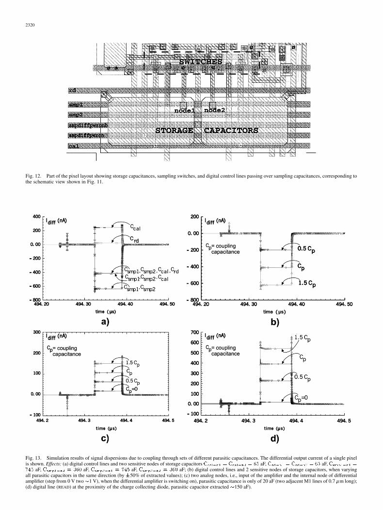
Fig. 12. Part of the pixel layout showing storage capacitances, sampling switches, and digital control lines passing over sampling capacitances, corresponding tothe schematic view shown in Fig. 11.
Fig. 13. Simulation results of signal dispersions due to coupling through sets of different parasitic capacitances. The differential output current of a single pixelis shown. Effects: (a) digital control lines and two sensitive nodes of storage capacitors C = C = 65 aF, C = C = 65 aF, C =
745 aF, C = 360 aF, C = 745 aF, C = 360 aF; (b) digital control lines and 2 sensitive nodes of storage capacitors, when varyingall parasitic capacitors in the same direction (by �50% of extracted values); (c) two analog nodes, i.e., input of the amplifier and the internal node of differentialamplifier (step from 0 V two�1 V), when the differential amplifier is switching on), parasitic capacitance is only of 20 aF (two adjacent M1 lines of 0.7 �m long);(d) digital line (READ) at the proximity of the charge collecting diode, parasitic capacitor extracted �150 aF).
2321
simulation. Following curves in Fig. 13 show the influence ofvaried coupling capacitances and different sources of couplingonto the output current. Assuming realistic dispersion level ofparasitic capacitance, the results are quantitatively in agreementwith measurements.
VII. RESULTS SUMMARY
The important design features and main parameters extractedfrom the first measurements of MIMOSA VI are summarized inTable I. Noise levels reported correspond to the calculated dif-ference between the levels in CALIBRATION and READOUTphases, as simulated with ELDO. The pixel dispersions are re-ferred as to the pixel-to-pixel pedestal variations between the dclevels for the two phases in the pixel readout cycle.
VIII. CONCLUSION AND PERSPECTIVES
The MIMOSA VI chip features the first step toward the devel-opment of a smart MAPS based vertex detector. The function-ality of the column-based comparators has been demonstrated.The possibility of in-pixel integration of double sampling oper-ation allowing reduced intrinsic pixel-to-pixel output level dis-persions has also been ascertained. The limited efficiency of thecurrent implementation of zero-suppression is attributed to theparasitic stray and substrate capacitances. Improvement can beachieved by careful circuit and layout studies. This includes in-creasing of the gain of the in-pixel amplifier to about ten or
more, reducing the number of control lines, replacing the inputin-pixel source follower by direct ac-coupling to the charge sen-sitive element, special care about fully symmetrical layout ofcritical parts, and minimized coupling by pushing away “trucu-lent” lines.
Despite the drawback of high pedestal dispersions, the MI-MOSA VI chip validated the possibility of in-pixel samplingand storing signals from two different time slots. The numberof memory cells can be extended in future circuits, allowingmultiple and fast signal sampling inside beam bunch trains. Thestored information (snapshots) can be read out between trains atlower speed. This approach would allow dealing with high oc-cupancy in some experiments.
REFERENCES
[1] G. Deptuch et al., “Design and testing of monolithic active pixel sensorsfor charged particle tracking,” IEEE Trans. Nucl. Sci., vol. 49, no. 2, pp.601–610, 2002.
[2] “TESLA, TDR, DESY 2001-011, ECFA 2001-209,”, TESLA Rep.2001-23, TESLA-FEL 2001-05, Mar. 2001.
[3] Y. Degerli, N. T. Fourches, M. Rouger, and P. Lutz, “A low powerautozeroed high speed comparator for the readout chain of a CMOSMAPS based vertex detector,” IEEE Trans. Nucl. Sci., vol. 50, no. 5,pp. 1709–1717, 2003.
[4] G. Deptuch, W. Dulinski, Y. Gornushkin, C. Hu-Guo, and I. Valin,“Monolithic active pixel sensors with on-pixel amplification and doublesampling operation,” Nucl. Instrum. Meth., vol. A 512, pp. 299–309,2003.
[5] B. Dierickx, G. Meynants, and D. Scheffer, “Near 100% fill factorCMOS active pixels,” in Proc. IEEE CCD&AIS Workshop, Brugge,Belgium, June 5–7, 1997, p. P1.
Related Documents