This document is downloaded from DR-NTU, Nanyang Technological University Library, Singapore. Title Mono-distributed single-walled carbon nanotube channel in field effect transistors (FETs) using electrostatic atomization deposition Author(s) Fam, Derrick Wen Hui; Tok, Alfred Iing Yoong Citation Fam, D. W. H., & Tok, A. I. Y. (2009). Mono-distributed single-walled carbon nanotube channel in field effect transistors (FETs) using electrostatic atomization deposition. Journal of Colloid and Interface Science, 338, 266-269. Date 2009 URL http://hdl.handle.net/10220/6959 Rights © 2009 Elsevier. This is the author created version of a work that has been peer reviewed and accepted for publication by Journal of Colloid and Interface Science, Elsevier. It incorporates referee’s comments but changes resulting from the publishing process, such as copyediting, structural formatting, may not be reflected in this document. The published version is available at: http://dx.doi.org/10.1016/j.jcis.2009.06.003.

Welcome message from author
This document is posted to help you gain knowledge. Please leave a comment to let me know what you think about it! Share it to your friends and learn new things together.
Transcript

This document is downloaded from DR-NTU, Nanyang Technological
University Library, Singapore.
TitleMono-distributed single-walled carbon nanotube channelin field effect transistors (FETs) using electrostaticatomization deposition
Author(s) Fam, Derrick Wen Hui; Tok, Alfred Iing Yoong
Citation
Fam, D. W. H., & Tok, A. I. Y. (2009). Mono-distributedsingle-walled carbon nanotube channel in field effecttransistors (FETs) using electrostatic atomizationdeposition. Journal of Colloid and Interface Science, 338,266-269.
Date 2009
URL http://hdl.handle.net/10220/6959
Rights
© 2009 Elsevier. This is the author created version of awork that has been peer reviewed and accepted forpublication by Journal of Colloid and Interface Science,Elsevier. It incorporates referee’s comments but changesresulting from the publishing process, such ascopyediting, structural formatting, may not be reflected inthis document. The published version is available at:http://dx.doi.org/10.1016/j.jcis.2009.06.003.

Elsevier Editorial System(tm) for Journal of Colloid and Interface Science
Manuscript Draft
Manuscript Number: JCIS-08-1389R1
Title: Mono-distributed Single-walled Carbon Nanotube Channel in Field Effect Transistors (FETs)
using Electrostatic Atomization Deposition
Article Type: Regular Article
Section/Category: K. Clusters, Nanomaterials and Self-Organization
Keywords: Carbon nanotubes, electrostatic atomization, monodispersed
Corresponding Author: Dr. Alfred Tok,
Corresponding Author's Institution: Nanyang Technological University
First Author: Derrick Fam
Order of Authors: Derrick Fam; Alfred Tok
Abstract: This communication reports on the novel work of creating a transistor channel based on
functionalized Single Walled Carbon Nanotubes (SWNTs) via Electrostatic Atomization Deposition.
The current method of drop-cast though convenient was unable to produce replicable transistor
device due to its inherent inability in controlling the volume of liquid being drop-cast. Hence, this
method of electrostatic atomization was introduced to consistently obtain a uniformly distributed
SWNT channel resulting in a good transistor device.
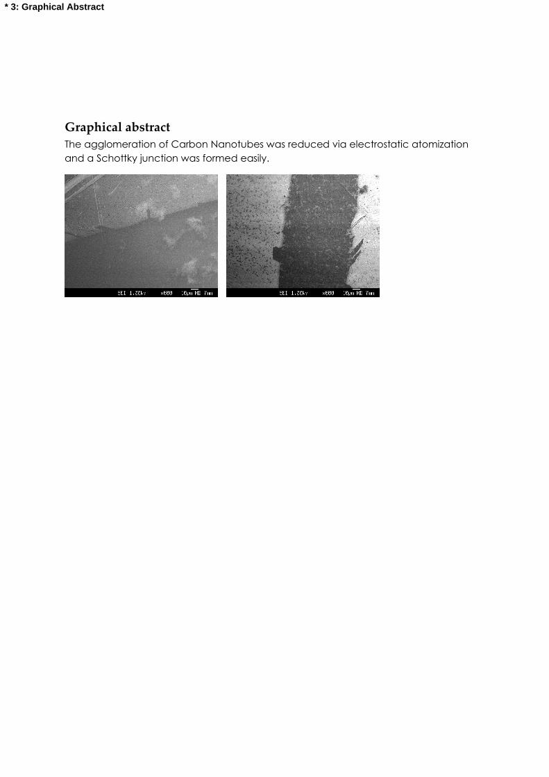
Graphical abstractThe agglomeration of Carbon Nanotubes was reduced via electrostatic atomization and a Schottky junction was formed easily.
* 3: Graphical Abstract

1 2 3 4 5 6 7 8 9 10 11 12 13 14 15 16 17 18 19 20 21 22 23 24 25 26 27 28 29 30 31 32 33 34 35 36 37 38 39 40 41 42 43 44 45 46 47 48 49 50 51 52 53 54 55 56 57 58 59 60 61 62 63 64 65
Mono-distributed Single-walled Carbon Nanotube Channel in Field
Effect Transistors (FETs) using Electrostatic Atomization
Deposition
D.W.H. Fam & A.I.Y. Tok*
School of Materials Science and Engineering, Nanyang Technological University, Block N4.1, 50
Nanyang Avenue, Singapore 639798, Tel: (65) 6790 4142, Fax: (65) 6790 9081
Abstract
This communication reports on the novel work of creating a transistor channel based on
functionalized Single Walled Carbon Nanotubes (SWNTs) via Electrostatic Atomization
Deposition. The current method of drop-cast though convenient was unable to produce
replicable transistor device due to its inherent inability in controlling the volume of liquid
being drop-cast. Hence, this method of electrostatic atomization was introduced to
consistently obtain a uniformly distributed SWNT channel resulting in a good transistor
device.
Keywords: Carbon nanotubes, electrostatic atomization, monodispersed
* 4a: Marked highlighted manuscript

1 2 3 4 5 6 7 8 9 10 11 12 13 14 15 16 17 18 19 20 21 22 23 24 25 26 27 28 29 30 31 32 33 34 35 36 37 38 39 40 41 42 43 44 45 46 47 48 49 50 51 52 53 54 55 56 57 58 59 60 61 62 63 64 65
1. Introduction
Field effect transistors (FETs) have found their uses in many applications in the
microelectronics industry [1]. FETs typically consist of a gate, where the bias would be
applied, a source and a drain electrode. Across the source and drain electrode is the
channel which typically comprise of a semi-conductive material. There are many
materials used as the semi-conductive channel [2] and Single-walled Carbon Nanotubes
(SWCNTs) are one of them [3]. SWCNTs are essentially rolled graphene sheets which
are of 0.4-3nm in diameter. They consist of sp2 hybridized carbon atoms and have three
out of the four outer shell electrons participate in bonding with neighbouring carbon
atoms while the fourth carbon is in a p-orbital perpendicular to the hexagonal lattice [4].
CNTs are used to fabricate field effect transistors due to their excellent electron mobility
[5] which is very suitable for applications in high-speed transistors, memory devices and
also chemical or biological sensors. There are essentially two different methods of
fabrication of these CNT devices namely, via CNT growth and drop cast. Growing CNTs
on the surface of a substrate involves the use of a catalyst [6-10] via a chemical vapor
deposition (CVD) method [7, 11, 12] or by an arc discharge method [1, 13]. Although this
method of deposition yields good transistor devices, the surface chemistries of the CNTs
cannot be modified to suit different purposes; functionalization and decoration of the
tubes could not be done easily in situ should the CNT devices be fabricated by tube
growth. Functionalization and decoration of CNTs is done for a variety of sensing
applications [4, 13-18] as well as to modify their electronic properties [19]. Another
common method of fabrication of these CNT devices would be via drop-cast [20].
However this method of deposition results in much agglomeration and hence a
consistent device characteristic will not be achievable. Hence a suitable method had to
be found to both allow for easy manipulation of CNT surface chemistry and creating
consistent transistor devices. Electrospraying has been explored as a method of

1 2 3 4 5 6 7 8 9 10 11 12 13 14 15 16 17 18 19 20 21 22 23 24 25 26 27 28 29 30 31 32 33 34 35 36 37 38 39 40 41 42 43 44 45 46 47 48 49 50 51 52 53 54 55 56 57 58 59 60 61 62 63 64 65
depositing double-walled carbon nanotubes and it yielded low-density bundles and even
isolated double-walled carbon nanotubes [21]. Electrostatic atomization (EA) is a form of
deposition in which a jet of liquid is exposed to an electric field which leads to a
dispersion of the particles arising from either liquid polarization or free charge repulsion.
This jet of liquid will then break into droplets when it is released at a controlled flow rate
through a stainless steel needle [22]. The EA schematic is as seen in Figure 1. The
solution is pushed into the capillary tube and into the needle at a constant flow rate
whereby it experiences an electric field set up due to the potential difference between
the needle tip and the ground electrode. The field at the tip then overcomes the surface
tension of the liquid which results in a jet forming from the breakup of the liquid surface.
This jet consists of extremely small liquid droplets which would be accelerated towards
the stage, which is below the ground electrode hence depositing the liquid droplets onto
the substrate on the stage. EA has been widely applied since its initial use on paints [23].
EA has also been applied to hydrocarbons [24, 25], ceramics [26] and a variety of other
materials [27] to obtain self-assembled nanostructures [28]. However, one of the most
poignant uses of EA was to create a mono-distributed thin film [29, 30]. Hence, this
paper shows a novel method of preparing a transistor with a mono-distributed network of
CNT via electrostatic atomization.
2. Materials
Single-walled carbon nanotubes (SWNTs) were bought from Carbon Solutions, Inc. and
were used as bought. The SWNTs are then suspended in ethanol due to its low surface
tension so that a stable cone-jet mode can be reached when it is atomized. SWCNTs,
because of their nanoscale dimensions, they typically agglomerate in polar solvents like
water. Hence surfactants would normally be used to suspend the nanotubes in the
solvents and in this work; poly (4-vinyl pyridine) (P4VP) bought from Sigma Aldrich was
used as the surfactant.

1 2 3 4 5 6 7 8 9 10 11 12 13 14 15 16 17 18 19 20 21 22 23 24 25 26 27 28 29 30 31 32 33 34 35 36 37 38 39 40 41 42 43 44 45 46 47 48 49 50 51 52 53 54 55 56 57 58 59 60 61 62 63 64 65
3. Methods
Sonication was applied to separate the nanotube bundles. After which, centrifugation
was done to separate the free nanotubes from the agglomerated ones. S1 is a solution
of 99.99wt% absolute ethanol and 0.01wt% P3 SWNTs (functionalized with carboxylic
acid (-COOH) groups). S1 was made to sonicate for 20mins and centrifuged at
14000rpm for 75mins. The suspension characteristics like its conductivity, surface
tension, viscosity and dielectric constant were then measured with a SCHOTT
conductivity meter, Contraves low shear rheometer, contact angle measuring equipment
and the Alpha TDR 5000 meter respectively. The extracted supernatant solution was
then drop-cast or electrosprayed onto the device (Figure 2) channel as the
semiconductor layer using a pipette. The stable cone jet mode for EA was achieved at
0.07ml/hr and the process was done for 3mins. Field emission scanning electron
micrographs were then taken of the channel to compare its dispersity. The transfer
characteristic, namely the drain current (ID) against drain voltage (VD) with different gate
voltages (VG) was then measured using a Keithley 4200 parametric analyzer. The ID was
swept from -5V to 5V and VG was stepped from -5V to 5V.
4. Results and Discussion
4.1 Fluid properties of test solutions
The properties of the suspension of SWNTs in ethanol solution, namely its conductivity,
surface tension and viscosity has to be within (10-3 – 10-7 S/m), (10 – 100 dy/cm) and 10-3
Pa s respectively. The conductivity was measured to be 0.06µS/m, the surface tension
29.2dy/cm, viscosity 1.1 x 10⁻³ Pa.s and the dielectric constant 23.04.
4.2 Domains of the cone jet range
The cone jet mode takes place when the meniscus begins to merge in a conical shape.
Upon its onset, the cone would take an elongated shape and the cone gets more
defined as the voltage increases slowly while maintaining an optimum flow rate.

1 2 3 4 5 6 7 8 9 10 11 12 13 14 15 16 17 18 19 20 21 22 23 24 25 26 27 28 29 30 31 32 33 34 35 36 37 38 39 40 41 42 43 44 45 46 47 48 49 50 51 52 53 54 55 56 57 58 59 60 61 62 63 64 65
However, if the applied voltage is too high, the electric potential increases and would in
turn result in multi-jet modes. If the applied voltage is too low, it would decrease in
electric potential and result in dripping modes. At a very low or high flow rate, the stable
cone jet mode would not be established easily. There are three phases in the cone jet
range, namely cone jet hysteresis, cone jet initiation and cone jet top limit. Hysteresis
takes place by decreasing the voltage while maintaining the cone jet mode. Cone jet
initiation refers to the initial occurrence when the cone jet mode is stabilized. It was
found that for the suspension, a stable cone jet mode could be reached with the spray
parameters of 0.07 ml/hr at 3.61kV.
4.3 CNT device fabricated by drop-cast method.
The device channel fabricated by drop cast shows much agglomeration as seen in
Figure 3. This is due to the low surface-area to volume ratio of the drop hence
evaporation of the drop is slow which gives time for agglomeration of the nanoparticles.
Furthermore, devices prepared by drop-cast method more often than not yields metallic
junctions rather than Schottky ones as seen in Figure 4. This is due to the large volume
of solution that is usually present in a single drop. This will result in the metallic tubes
conducting most of the charges instead of the semiconducting tubes. In addition, there is
no way of controlling exactly the amount of solution being dropped onto the channel.
Hence the devices are usually not replicable. Devices fabricated by drop cast usually
have CNTs all over rather than having them localized in the channel itself. This is
because the drops are usually large and its diameter spans larger than the channel
width.
4.4 CNT device fabricated by electrostatic atomization
The devices that were fabricated via electrostatic atomization could be reproduced with
much consistency. When the SWNTs in the ethanol solution was sprayed and dispersed
1 2 3 4 5 6 7 8 9 10 11 12 13 14 15 16 17 18 19 20 21 22 23 24 25 26 27 28 29 30 31 32 33 34 35 36 37 38 39 40 41 42 43 44 45 46 47 48 49 50 51 52 53 54 55 56 57 58 59 60 61 62 63 64 65
onto the substrate, evaporation occurs almost instantaneously and leaves the SWNTs
on the substrate in its un-agglomerated state.
4.4.1 CNT Device fabricated using S1
S1 is a suspension of CNTs functionalized with –COOH groups in ethanol. The CNTs
which were functionalized are now polar and can suspend in ethanol without any aid
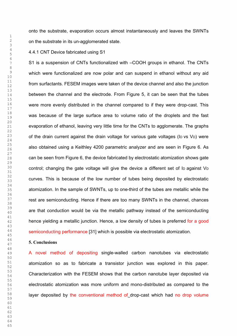
from surfactants. FESEM images were taken of the device channel and also the junction
between the channel and the electrode. From Figure 5, it can be seen that the tubes
were more evenly distributed in the channel compared to if they were drop-cast. This
was because of the large surface area to volume ratio of the droplets and the fast
evaporation of ethanol, leaving very little time for the CNTs to agglomerate. The graphs
of the drain current against the drain voltage for various gate voltages (ID vs VD) were
also obtained using a Keithley 4200 parametric analyzer and are seen in Figure 6. As
can be seen from Figure 6, the device fabricated by electrostatic atomization shows gate
control; changing the gate voltage will give the device a different set of ID against VD
curves. This is because of the low number of tubes being deposited by electrostatic
atomization. In the sample of SWNTs, up to one-third of the tubes are metallic while the
rest are semiconducting. Hence if there are too many SWNTs in the channel, chances
are that conduction would be via the metallic pathway instead of the semiconducting
hence yielding a metallic junction. Hence, a low density of tubes is preferred for a good
semiconducting performance [31] which is possible via electrostatic atomization.
5. Conclusions
A novel method of depositing single-walled carbon nanotubes via electrostatic
atomization so as to fabricate a transistor junction was explored in this paper.
Characterization with the FESEM shows that the carbon nanotube layer deposited via
electrostatic atomization was more uniform and mono-distributed as compared to the
layer deposited by the conventional method of drop-cast which had no drop volume

1 2 3 4 5 6 7 8 9 10 11 12 13 14 15 16 17 18 19 20 21 22 23 24 25 26 27 28 29 30 31 32 33 34 35 36 37 38 39 40 41 42 43 44 45 46 47 48 49 50 51 52 53 54 55 56 57 58 59 60 61 62 63 64 65
control. Furthermore, the ID vs VD measurement from the parametric analyzer shows that
gate control was achieved with a metastable solution of carboxylic acid group
functionalized carbon nanotubes in ethanol which were deposited by electrostatic
atomization. Further study of the electrostatic deposition of modified tubes will be carried
out in the future.
Acknowledgements
We would like to express our thanks to School of Materials Science and Engineering,
Nanyang Technological University for financial support.

1 2 3 4 5 6 7 8 9 10 11 12 13 14 15 16 17 18 19 20 21 22 23 24 25 26 27 28 29 30 31 32 33 34 35 36 37 38 39 40 41 42 43 44 45 46 47 48 49 50 51 52 53 54 55 56 57 58 59 60 61 62 63 64 65
References
[1] S. Iijima, T. Ichihashi, Nature 1993, 363, 603.
[2] L. Wang, D. Fine, A. Dodabalapur, Applied Physics Letters 2004, 85, 6386.
[3] R. Martel, T. Schmidt, H. R. Shea, T. Hertel, P. Avouris, Applied Physics Letters 1998,
73, 2447.
[4] S. N. Kim, J. F. Rusling, F. Papadimitrakopoulos, Advanced Materials 2007, 19, 3214.
[5] T. Durkop, S. A. Getty, E. Cobas, M. S. Fuhrer, Nano Letters 2004, 4, 35.
[6] P. M. Ajayan, J. M. Lambert, P. Bernier, L. Barbedette, C. Colliex, J. M. Planeix,
Chemical Physics Letters 1993, 215, 509.
[7] C. Bae-Horng, L. Po-Yuan, W. Jeng-Hua, T. Ming-Jinn, H. Chien-Liang, C. Tien-
Sheng, L. Horng-Chih, H. Tiao-Yuan, Electrochemical and Solid-State Letters 2005, 8, 290.
[8] D. S. Bethune, C. H. Kiang, M. S. de Vries, G. Gorman, R. Savoy, J. Vazquez, R.
Beyers, Nature 1993, 363, 605.
[9] Y. Wei-Chang, Y. Tsung-Yeh, Y. Tri-Rung, Carbon 2007, 45, 1679.
[10] W. Wongwiriyapan, et al., Japanese Journal of Applied Physics, Part 1 2005, 44, 8227.
[11] M. Chhowalla, et al., Journal of Applied Physics 2001, 90, 5308.
[12] L. Valentini, I. Armentano, J. M. Kenny, C. Cantalini, L. Lozzi, S. Santucci, Applied
Physics Letters 2003, 82, 961.
[13] T.W. Ebbesen and P.M. Ajayan, Nature 1992, 358, 6383
[14] Fam, D.W.H., et al., Sensors and Actuators B: Chemical. In Press, Corrected Proof.
[15] X. Jining, et al., Nanotechnology 2007, 18, 6.
[16] E.H. Espinosa, et al., Thin Solid Films 2007, 515, 23.
[17] M. Chen and A. Gelperin, Nano Letters 2005, 5, 9.
[18] S. Mubeen, et al., Journal of Physical Chemistry C 2007. 111,17.
[19] W. Chenchen, Z. Gang, W. Jian, G. Bing-Lin, D. Wenhui, Applied Physics Letters 2006,
89, 173130.

1 2 3 4 5 6 7 8 9 10 11 12 13 14 15 16 17 18 19 20 21 22 23 24 25 26 27 28 29 30 31 32 33 34 35 36 37 38 39 40 41 42 43 44 45 46 47 48 49 50 51 52 53 54 55 56 57 58 59 60 61 62 63 64 65
[20] J. Maklin, T. Mustonen, K. Kordas, S. Saukko, G. Toth, J. Vahakangas, Physica
Status Solidi (B) 2007, 244, 4298.
[21] J.N. O'Shea et al., Nanotechnology 2007. 18, 3.
[22] S. N. Jayasinghe, M. J. Edirisinghe, Journal of the European Ceramic Society 2004, 24,
2203.
[23] Anon, Machinery (New York) 1951, 58, 185.
[24] W. Lehr, W. Hiller, Journal of Electrostatics 1993, 30, 433.
[25] S. N. Jayasinghe, M. J. Edirisinghe, Journal of Materials Science Letters 2003, 22, 1443.
[26] W. D. Teng, Z. A. Huneiti, W. Machowski, J. R. G. Evans, M. J. Edirisinghe, W.
Balachandran, Journal of Materials Science Letters 1997, 16, 1017.
[27] M. Lohmann, H. Kirsch, A. Schmidt-Ott, Journal of Aerosol Science 1996, 27, 185.
[28] S. N. Jayasinghe, Physica E 2006, 33, 398.
[29] C. J. Hogan Jr, P. Biswas, Journal of Aerosol Science 2008, 39, 432.
[30] W. Deng, J. F. Klemic, X. Li, M. A. Reed, A. Gomez, Journal of Aerosol Science
2006, 37, 696.
[31] M. Shiraishi, T. Takenobu, T. Iwai et al., Chemical Physics Letters 2004, 394 (1-3), 110-
113.

1 2 3 4 5 6 7 8 9 10 11 12 13 14 15 16 17 18 19 20 21 22 23 24 25 26 27 28 29 30 31 32 33 34 35 36 37 38 39 40 41 42 43 44 45 46 47 48 49 50 51 52 53 54 55 56 57 58 59 60 61 62 63 64 65
Figures
Figure 1. Schematic of the Electrostatic Atomization setup which shows the needle under DC
voltage bias and the computer connected to the microscopic camera recording the shape of the jet.
Figure 2. Transistor with back gate
Computer
High voltage DC source
Ground electrode
Light
source
Microscopic camera
stage
Needle held in resin
Capillary tubeSyringe pump

1 2 3 4 5 6 7 8 9 10 11 12 13 14 15 16 17 18 19 20 21 22 23 24 25 26 27 28 29 30 31 32 33 34 35 36 37 38 39 40 41 42 43 44 45 46 47 48 49 50 51 52 53 54 55 56 57 58 59 60 61 62 63 64 65
Figure 3. FESEM image showing agglomeration of CNTs, seen in the bottom right
Figure 4. Metallic CNT junction created from drop-cast method
1 2 3 4 5 6 7 8 9 10 11 12 13 14 15 16 17 18 19 20 21 22 23 24 25 26 27 28 29 30 31 32 33 34 35 36 37 38 39 40 41 42 43 44 45 46 47 48 49 50 51 52 53 54 55 56 57 58 59 60 61 62 63 64 65
Figure 5. FESEM image of monodispersed SWNTs deposited by EA in channel
Figure 6. CNT device fabricated by EA showing gate control

1 2 3 4 5 6 7 8 9 10 11 12 13 14 15 16 17 18 19 20 21 22 23 24 25 26 27 28 29 30 31 32 33 34 35 36 37 38 39 40 41 42 43 44 45 46 47 48 49 50 51 52 53 54 55 56 57 58 59 60 61 62 63 64 65
Mono-distributed Single-walled Carbon Nanotube Channel in Field
Effect Transistors (FETs) using Electrostatic Atomization
Deposition
D.W.H. Fam & A.I.Y. Tok*
School of Materials Science and Engineering, Nanyang Technological University, Block N4.1, 50
Nanyang Avenue, Singapore 639798, Tel: (65) 6790 4142, Fax: (65) 6790 9081
Abstract
This communication reports on the novel work of creating a transistor channel based on
functionalized Single Walled Carbon Nanotubes (SWNTs) via Electrostatic Atomization
Deposition. The current method of drop-cast though convenient was unable to produce
replicable transistor device due to its inherent inability in controlling the volume of liquid
being drop-cast. Hence, this method of electrostatic atomization was introduced to
consistently obtain a uniformly distributed SWNT channel resulting in a good transistor
device.
Keywords: Carbon nanotubes, electrostatic atomization, monodispersed
* 4c: Unmarked Revised manuscriptClick here to view linked References

1 2 3 4 5 6 7 8 9 10 11 12 13 14 15 16 17 18 19 20 21 22 23 24 25 26 27 28 29 30 31 32 33 34 35 36 37 38 39 40 41 42 43 44 45 46 47 48 49 50 51 52 53 54 55 56 57 58 59 60 61 62 63 64 65
1. Introduction
Field effect transistors (FETs) have found their uses in many applications in the
microelectronics industry [1]. FETs typically consist of a gate, where the bias would be
applied, a source and a drain electrode. Across the source and drain electrode is the
channel which typically comprise of a semi-conductive material. There are many
materials used as the semi-conductive channel [2] and Single-walled Carbon Nanotubes
(SWCNTs) are one of them [3]. SWCNTs are essentially rolled graphene sheets which
are of 0.4-3nm in diameter. They consist of sp2 hybridized carbon atoms and have three
out of the four outer shell electrons participate in bonding with neighbouring carbon
atoms while the fourth carbon is in a p-orbital perpendicular to the hexagonal lattice [4].
CNTs are used to fabricate field effect transistors due to their excellent electron mobility
[5] which is very suitable for applications in high-speed transistors, memory devices and
also chemical or biological sensors. There are essentially two different methods of
fabrication of these CNT devices namely, via CNT growth and drop cast. Growing CNTs
on the surface of a substrate involves the use of a catalyst [6-10] via a chemical vapor
deposition (CVD) method [7, 11, 12] or by an arc discharge method [1, 13]. Although this
method of deposition yields good transistor devices, the surface chemistries of the CNTs
cannot be modified to suit different purposes; functionalization and decoration of the
tubes could not be done easily in situ should the CNT devices be fabricated by tube
growth. Functionalization and decoration of CNTs is done for a variety of sensing
applications [4, 13-18] as well as to modify their electronic properties [19]. Another
common method of fabrication of these CNT devices would be via drop-cast [20].
However this method of deposition results in much agglomeration and hence a
consistent device characteristic will not be achievable. Hence a suitable method had to
be found to both allow for easy manipulation of CNT surface chemistry and creating
consistent transistor devices. Electrospraying has been explored as a method of

1 2 3 4 5 6 7 8 9 10 11 12 13 14 15 16 17 18 19 20 21 22 23 24 25 26 27 28 29 30 31 32 33 34 35 36 37 38 39 40 41 42 43 44 45 46 47 48 49 50 51 52 53 54 55 56 57 58 59 60 61 62 63 64 65
depositing double-walled carbon nanotubes and it yielded low-density bundles and even
isolated double-walled carbon nanotubes [21]. Electrostatic atomization (EA) is a form of
deposition in which a jet of liquid is exposed to an electric field which leads to a
dispersion of the particles arising from either liquid polarization or free charge repulsion.
This jet of liquid will then break into droplets when it is released at a controlled flow rate
through a stainless steel needle [22]. The EA schematic is as seen in Figure 1. The
solution is pushed into the capillary tube and into the needle at a constant flow rate
whereby it experiences an electric field set up due to the potential difference between
the needle tip and the ground electrode. The field at the tip then overcomes the surface
tension of the liquid which results in a jet forming from the breakup of the liquid surface.
This jet consists of extremely small liquid droplets which would be accelerated towards
the stage, which is below the ground electrode hence depositing the liquid droplets onto
the substrate on the stage. EA has been widely applied since its initial use on paints [23].
EA has also been applied to hydrocarbons [24, 25], ceramics [26] and a variety of other
materials [27] to obtain self-assembled nanostructures [28]. However, one of the most
poignant uses of EA was to create a mono-distributed thin film [29, 30]. Hence, this
paper shows a novel method of preparing a transistor with a mono-distributed network of
CNT via electrostatic atomization.
2. Materials
Single-walled carbon nanotubes (SWNTs) were bought from Carbon Solutions, Inc. and
were used as bought. The SWNTs are then suspended in ethanol due to its low surface
tension so that a stable cone-jet mode can be reached when it is atomized. SWCNTs,
because of their nanoscale dimensions, they typically agglomerate in polar solvents like
water. Hence surfactants would normally be used to suspend the nanotubes in the
solvents and in this work; poly (4-vinyl pyridine) (P4VP) bought from Sigma Aldrich was
used as the surfactant.

1 2 3 4 5 6 7 8 9 10 11 12 13 14 15 16 17 18 19 20 21 22 23 24 25 26 27 28 29 30 31 32 33 34 35 36 37 38 39 40 41 42 43 44 45 46 47 48 49 50 51 52 53 54 55 56 57 58 59 60 61 62 63 64 65
3. Methods
Sonication was applied to separate the nanotube bundles. After which, centrifugation
was done to separate the free nanotubes from the agglomerated ones. S1 is a solution
of 99.99wt% absolute ethanol and 0.01wt% P3 SWNTs (functionalized with carboxylic
acid (-COOH) groups). S1 was made to sonicate for 20mins and centrifuged at
14000rpm for 75mins. The suspension characteristics like its conductivity, surface
tension, viscosity and dielectric constant were then measured with a SCHOTT
conductivity meter, Contraves low shear rheometer, contact angle measuring equipment
and the Alpha TDR 5000 meter respectively. The extracted supernatant solution was
then drop-cast or electrosprayed onto the device (Figure 2) channel as the
semiconductor layer using a pipette. The stable cone jet mode for EA was achieved at
0.07ml/hr and the process was done for 3mins. Field emission scanning electron
micrographs were then taken of the channel to compare its dispersity. The transfer
characteristic, namely the drain current (ID) against drain voltage (VD) with different gate
voltages (VG) was then measured using a Keithley 4200 parametric analyzer. The ID was
swept from -5V to 5V and VG was stepped from -5V to 5V.
4. Results and Discussion
4.1 Fluid properties of test solutions
The properties of the suspension of SWNTs in ethanol solution, namely its conductivity,
surface tension and viscosity has to be within (10-3 – 10-7 S/m), (10 – 100 dy/cm) and 10-3
Pa s respectively. The conductivity was measured to be 0.06µS/m, the surface tension
29.2dy/cm, viscosity 1.1 x 10⁻³ Pa.s and the dielectric constant 23.04.
4.2 Domains of the cone jet range
The cone jet mode takes place when the meniscus begins to merge in a conical shape.
Upon its onset, the cone would take an elongated shape and the cone gets more
defined as the voltage increases slowly while maintaining an optimum flow rate.
1 2 3 4 5 6 7 8 9 10 11 12 13 14 15 16 17 18 19 20 21 22 23 24 25 26 27 28 29 30 31 32 33 34 35 36 37 38 39 40 41 42 43 44 45 46 47 48 49 50 51 52 53 54 55 56 57 58 59 60 61 62 63 64 65
However, if the applied voltage is too high, the electric potential increases and would in
turn result in multi-jet modes. If the applied voltage is too low, it would decrease in
electric potential and result in dripping modes. At a very low or high flow rate, the stable
cone jet mode would not be established easily. There are three phases in the cone jet
range, namely cone jet hysteresis, cone jet initiation and cone jet top limit. Hysteresis
takes place by decreasing the voltage while maintaining the cone jet mode. Cone jet
initiation refers to the initial occurrence when the cone jet mode is stabilized. It was
found that for the suspension, a stable cone jet mode could be reached with the spray
parameters of 0.07 ml/hr at 3.61kV.
4.3 CNT device fabricated by drop-cast method.
The device channel fabricated by drop cast shows much agglomeration as seen in
Figure 3. This is due to the low surface-area to volume ratio of the drop hence
evaporation of the drop is slow which gives time for agglomeration of the nanoparticles.
Furthermore, devices prepared by drop-cast method more often than not yields metallic
junctions rather than Schottky ones as seen in Figure 4. This is due to the large volume
of solution that is usually present in a single drop. This will result in the metallic tubes
conducting most of the charges instead of the semiconducting tubes. In addition, there is
no way of controlling exactly the amount of solution being dropped onto the channel.
Hence the devices are usually not replicable. Devices fabricated by drop cast usually
have CNTs all over rather than having them localized in the channel itself. This is
because the drops are usually large and its diameter spans larger than the channel
width.
4.4 CNT device fabricated by electrostatic atomization
The devices that were fabricated via electrostatic atomization could be reproduced with
much consistency. When the SWNTs in the ethanol solution was sprayed and dispersed

1 2 3 4 5 6 7 8 9 10 11 12 13 14 15 16 17 18 19 20 21 22 23 24 25 26 27 28 29 30 31 32 33 34 35 36 37 38 39 40 41 42 43 44 45 46 47 48 49 50 51 52 53 54 55 56 57 58 59 60 61 62 63 64 65
onto the substrate, evaporation occurs almost instantaneously and leaves the SWNTs
on the substrate in its un-agglomerated state.
4.4.1 CNT Device fabricated using S1
S1 is a suspension of CNTs functionalized with –COOH groups in ethanol. The CNTs
which were functionalized are now polar and can suspend in ethanol without any aid
from surfactants. FESEM images were taken of the device channel and also the junction
between the channel and the electrode. From Figure 5, it can be seen that the tubes
were more evenly distributed in the channel compared to if they were drop-cast. This
was because of the large surface area to volume ratio of the droplets and the fast
evaporation of ethanol, leaving very little time for the CNTs to agglomerate. The graphs
of the drain current against the drain voltage for various gate voltages (ID vs VD) were
also obtained using a Keithley 4200 parametric analyzer and are seen in Figure 6. As
can be seen from Figure 6, the device fabricated by electrostatic atomization shows gate
control; changing the gate voltage will give the device a different set of ID against VD
curves. This is because of the low number of tubes being deposited by electrostatic
atomization. In the sample of SWNTs, up to one-third of the tubes are metallic while the
rest are semiconducting. Hence if there are too many SWNTs in the channel, chances
are that conduction would be via the metallic pathway instead of the semiconducting
hence yielding a metallic junction. Hence, a low density of tubes is preferred for a good
semiconducting performance [31] which is possible via electrostatic atomization.
5. Conclusions
A novel method of depositing single-walled carbon nanotubes via electrostatic
atomization so as to fabricate a transistor junction was explored in this paper.
Characterization with the FESEM shows that the carbon nanotube layer deposited via
electrostatic atomization was more uniform and mono-distributed as compared to the
layer deposited by the conventional method of drop-cast which had no drop volume

1 2 3 4 5 6 7 8 9 10 11 12 13 14 15 16 17 18 19 20 21 22 23 24 25 26 27 28 29 30 31 32 33 34 35 36 37 38 39 40 41 42 43 44 45 46 47 48 49 50 51 52 53 54 55 56 57 58 59 60 61 62 63 64 65
control. Furthermore, the ID vs VD measurement from the parametric analyzer shows that
gate control was achieved with a metastable solution of carboxylic acid group
functionalized carbon nanotubes in ethanol which were deposited by electrostatic
atomization. Further study of the electrostatic deposition of modified tubes will be carried
out in the future.
Acknowledgements
We would like to express our thanks to School of Materials Science and Engineering,
Nanyang Technological University for financial support.

1 2 3 4 5 6 7 8 9 10 11 12 13 14 15 16 17 18 19 20 21 22 23 24 25 26 27 28 29 30 31 32 33 34 35 36 37 38 39 40 41 42 43 44 45 46 47 48 49 50 51 52 53 54 55 56 57 58 59 60 61 62 63 64 65
References
[1] S. Iijima, T. Ichihashi, Nature 1993, 363, 603.
[2] L. Wang, D. Fine, A. Dodabalapur, Applied Physics Letters 2004, 85, 6386.
[3] R. Martel, T. Schmidt, H. R. Shea, T. Hertel, P. Avouris, Applied Physics Letters 1998,
73, 2447.
[4] S. N. Kim, J. F. Rusling, F. Papadimitrakopoulos, Advanced Materials 2007, 19, 3214.
[5] T. Durkop, S. A. Getty, E. Cobas, M. S. Fuhrer, Nano Letters 2004, 4, 35.
[6] P. M. Ajayan, J. M. Lambert, P. Bernier, L. Barbedette, C. Colliex, J. M. Planeix,
Chemical Physics Letters 1993, 215, 509.
[7] C. Bae-Horng, L. Po-Yuan, W. Jeng-Hua, T. Ming-Jinn, H. Chien-Liang, C. Tien-
Sheng, L. Horng-Chih, H. Tiao-Yuan, Electrochemical and Solid-State Letters 2005, 8, 290.
[8] D. S. Bethune, C. H. Kiang, M. S. de Vries, G. Gorman, R. Savoy, J. Vazquez, R.
Beyers, Nature 1993, 363, 605.
[9] Y. Wei-Chang, Y. Tsung-Yeh, Y. Tri-Rung, Carbon 2007, 45, 1679.
[10] W. Wongwiriyapan, et al., Japanese Journal of Applied Physics, Part 1 2005, 44, 8227.
[11] M. Chhowalla, et al., Journal of Applied Physics 2001, 90, 5308.
[12] L. Valentini, I. Armentano, J. M. Kenny, C. Cantalini, L. Lozzi, S. Santucci, Applied
Physics Letters 2003, 82, 961.
[13] T.W. Ebbesen and P.M. Ajayan, Nature 1992, 358, 6383
[14] Fam, D.W.H., et al., Sensors and Actuators B: Chemical. In Press, Corrected Proof.
[15] X. Jining, et al., Nanotechnology 2007, 18, 6.
[16] E.H. Espinosa, et al., Thin Solid Films 2007, 515, 23.
[17] M. Chen and A. Gelperin, Nano Letters 2005, 5, 9.
[18] S. Mubeen, et al., Journal of Physical Chemistry C 2007. 111,17.
[19] W. Chenchen, Z. Gang, W. Jian, G. Bing-Lin, D. Wenhui, Applied Physics Letters 2006,
89, 173130.

1 2 3 4 5 6 7 8 9 10 11 12 13 14 15 16 17 18 19 20 21 22 23 24 25 26 27 28 29 30 31 32 33 34 35 36 37 38 39 40 41 42 43 44 45 46 47 48 49 50 51 52 53 54 55 56 57 58 59 60 61 62 63 64 65
[20] J. Maklin, T. Mustonen, K. Kordas, S. Saukko, G. Toth, J. Vahakangas, Physica
Status Solidi (B) 2007, 244, 4298.
[21] J.N. O'Shea et al., Nanotechnology 2007. 18, 3.
[22] S. N. Jayasinghe, M. J. Edirisinghe, Journal of the European Ceramic Society 2004, 24,
2203.
[23] Anon, Machinery (New York) 1951, 58, 185.
[24] W. Lehr, W. Hiller, Journal of Electrostatics 1993, 30, 433.
[25] S. N. Jayasinghe, M. J. Edirisinghe, Journal of Materials Science Letters 2003, 22, 1443.
[26] W. D. Teng, Z. A. Huneiti, W. Machowski, J. R. G. Evans, M. J. Edirisinghe, W.
Balachandran, Journal of Materials Science Letters 1997, 16, 1017.
[27] M. Lohmann, H. Kirsch, A. Schmidt-Ott, Journal of Aerosol Science 1996, 27, 185.
[28] S. N. Jayasinghe, Physica E 2006, 33, 398.
[29] C. J. Hogan Jr, P. Biswas, Journal of Aerosol Science 2008, 39, 432.
[30] W. Deng, J. F. Klemic, X. Li, M. A. Reed, A. Gomez, Journal of Aerosol Science
2006, 37, 696.
[31] M. Shiraishi, T. Takenobu, T. Iwai et al., Chemical Physics Letters 2004, 394 (1-3), 110-
113.

1 2 3 4 5 6 7 8 9 10 11 12 13 14 15 16 17 18 19 20 21 22 23 24 25 26 27 28 29 30 31 32 33 34 35 36 37 38 39 40 41 42 43 44 45 46 47 48 49 50 51 52 53 54 55 56 57 58 59 60 61 62 63 64 65
Figures
Figure 1. Schematic of the Electrostatic Atomization setup which shows the needle under DC
voltage bias and the computer connected to the microscopic camera recording the shape of the jet.
Figure 2. Transistor with back gate
Computer
High voltage DC source
Ground electrode
Light
source
Microscopic camera
stage
Needle held in resin
Capillary tubeSyringe pump

1 2 3 4 5 6 7 8 9 10 11 12 13 14 15 16 17 18 19 20 21 22 23 24 25 26 27 28 29 30 31 32 33 34 35 36 37 38 39 40 41 42 43 44 45 46 47 48 49 50 51 52 53 54 55 56 57 58 59 60 61 62 63 64 65
Figure 3. FESEM image showing agglomeration of CNTs, seen in the bottom right
Figure 4. Metallic CNT junction created from drop-cast method

1 2 3 4 5 6 7 8 9 10 11 12 13 14 15 16 17 18 19 20 21 22 23 24 25 26 27 28 29 30 31 32 33 34 35 36 37 38 39 40 41 42 43 44 45 46 47 48 49 50 51 52 53 54 55 56 57 58 59 60 61 62 63 64 65
Figure 5. FESEM image of monodispersed SWNTs deposited by EA in channel
Figure 6. CNT device fabricated by EA showing gate control
Related Documents