Module-Integrated Converter Based on Cascaded Quasi-Z-Source Inverter with Differential Power Processing Capability for Photovoltaic Panels Under Partial Shading Masatoshi Uno, Member, IEEE, and Toshiki Shinohara Abstract—Conventional microinverter or module- integrated converter (MIC)-based photovoltaic (PV) systems are prone to be complex and costly because each MIC requires not only a boost converter to bridge a huge voltage gap between a PV panel and grid but also desirably a differential power processing (DPP) converter to preclude partial shading issues. This paper proposes a novel MIC based on cascaded quasi-Z-source inverters (qZSIs) with DPP capability. A traditional qZSI and voltage multiplier (VM)-based DPP converter are integrated into a single unit with sharing active switches and magnetic components, achieving system- and circuit-level simplifications. In addition, a novel control strategy utilizing two control freedoms of shoot-through duty cycle dst and modulation index M to simultaneously perform maximum power point tracking (MPPT) and DPP function, respectively, is also presented. A 150-W prototype for a standard PV panel consisting of three substrings was built, and experimental tests were performed emulating partial shading conditions. The results demonstrated that the proposed integrated qZSI could perform MPPT with satisfactory preventing partial shading issues while generating ac voltage at the inverter output. Keywords—Differential power processing (DPP) converter, module-integrated converter (MIC), quasi-Z- source inverter (qZSI), partial shading, photovoltaic system I. INTRODUCTION Microinverter or module-integrated converter (MIC)-based power conversion has become an important trend in photovoltaic (PV) systems. Each PV panel is installed with an MIC, allowing flexible system design and good scalability of the PV system because the number of panels can be arbitrarily extended by installing PV panels with MICs, without redesigning power conversion electronics. MIC-based PV systems, however, are prone to be complex and costly because boost and inverter stages are separately necessary [1], [2]. Voltages of standard 72-cell PV panels, in general, are as low as 30–50 V, and therefore, a high step-up boost converter is indispensable for PV panels to be connected with the grid through the inverter stage. Input-series–output- parallel converters are an alternative solution [3], but each converter must be a high step-up converter to bridge the huge voltage gap between a PV panel and a grid. Z-source inverters (ZSIs) have been vigorously studied and developed as a single-stage inverter with buck-boost capability [4], [5]. Among various kinds of ZSIs proposed, quasi-ZSIs (qZSIs) have gained popularity [6]. qZSIs utilize shoot-through (ST) states, during which inverter legs are short-circuited to charge their impedance network to achieve buck-boost operation. Furthermore, they offer high reliability since their impedance networks allow inverter legs to be short-circuited, whereas it is prohibited in traditional voltage-source inverters for preventing catastrophic failures. In order for PV panels to be connected with the grid, high step-up voltage conversion is mandatory even for qZSIs. Boost factors of ordinary qZSIs, however, are practically less than 2.0 [7] and are not high enough for PV panels. To achieve higher boost operations, various kinds of advanced ZSIs, such as diode- or capacitor-assisted extended-boost qZSIs [8], -source inverters [9], switched-inductor and switched-capacitor ZSIs [10]–[12], trans-ZSIs [13]–[15], and coupled-inductor ZSIs [16]–[18], have been proposed. These ZSIs achieve high boost- factor operations with shorter ST states than do traditional ZSIs. Cascaded MICs that interface PV panels with a single-phase grid in a modular structure have become a trend in PV systems [19], [20]. The modular structure reduces the voltage gain requirement for each MIC, allowing single-stage power conversion and higher switching frequency operations. In Fig. 1. Shaded and unshaded substrings in PV panel. This work was supported in part by Power Academy. M. Uno is with the College of Engineering, Ibaraki University, Hitachi 316-8511, Japan (e-mail: [email protected]). T. Shinohara is with Toyota Motor Corporation, Shizuoka, Japan (e- mail: chestnu[email protected]).

Welcome message from author
This document is posted to help you gain knowledge. Please leave a comment to let me know what you think about it! Share it to your friends and learn new things together.
Transcript
Module-Integrated Converter Based on Cascaded
Quasi-Z-Source Inverter with Differential Power
Processing Capability for Photovoltaic Panels Under
Partial Shading
Masatoshi Uno, Member, IEEE, and Toshiki Shinohara
Abstract—Conventional microinverter or module-
integrated converter (MIC)-based photovoltaic (PV)
systems are prone to be complex and costly because each
MIC requires not only a boost converter to bridge a huge
voltage gap between a PV panel and grid but also desirably
a differential power processing (DPP) converter to preclude
partial shading issues. This paper proposes a novel MIC
based on cascaded quasi-Z-source inverters (qZSIs) with
DPP capability. A traditional qZSI and voltage multiplier
(VM)-based DPP converter are integrated into a single unit
with sharing active switches and magnetic components,
achieving system- and circuit-level simplifications. In
addition, a novel control strategy utilizing two control
freedoms of shoot-through duty cycle dst and modulation
index M to simultaneously perform maximum power point
tracking (MPPT) and DPP function, respectively, is also
presented. A 150-W prototype for a standard PV panel
consisting of three substrings was built, and experimental
tests were performed emulating partial shading conditions.
The results demonstrated that the proposed integrated
qZSI could perform MPPT with satisfactory preventing
partial shading issues while generating ac voltage at the
inverter output.
Keywords—Differential power processing (DPP)
converter, module-integrated converter (MIC), quasi-Z-
source inverter (qZSI), partial shading, photovoltaic system
I. INTRODUCTION
Microinverter or module-integrated converter (MIC)-based
power conversion has become an important trend in
photovoltaic (PV) systems. Each PV panel is installed with an
MIC, allowing flexible system design and good scalability of
the PV system because the number of panels can be arbitrarily
extended by installing PV panels with MICs, without
redesigning power conversion electronics.
MIC-based PV systems, however, are prone to be complex
and costly because boost and inverter stages are separately
necessary [1], [2]. Voltages of standard 72-cell PV panels, in
general, are as low as 30–50 V, and therefore, a high step-up
boost converter is indispensable for PV panels to be connected
with the grid through the inverter stage. Input-series–output-
parallel converters are an alternative solution [3], but each
converter must be a high step-up converter to bridge the huge
voltage gap between a PV panel and a grid.
Z-source inverters (ZSIs) have been vigorously studied and
developed as a single-stage inverter with buck-boost capability
[4], [5]. Among various kinds of ZSIs proposed, quasi-ZSIs
(qZSIs) have gained popularity [6]. qZSIs utilize shoot-through
(ST) states, during which inverter legs are short-circuited to
charge their impedance network to achieve buck-boost
operation. Furthermore, they offer high reliability since their
impedance networks allow inverter legs to be short-circuited,
whereas it is prohibited in traditional voltage-source inverters
for preventing catastrophic failures.
In order for PV panels to be connected with the grid, high
step-up voltage conversion is mandatory even for qZSIs. Boost
factors of ordinary qZSIs, however, are practically less than 2.0
[7] and are not high enough for PV panels. To achieve higher
boost operations, various kinds of advanced ZSIs, such as
diode- or capacitor-assisted extended-boost qZSIs [8], -source
inverters [9], switched-inductor and switched-capacitor ZSIs
[10]–[12], trans-ZSIs [13]–[15], and coupled-inductor ZSIs
[16]–[18], have been proposed. These ZSIs achieve high boost-
factor operations with shorter ST states than do traditional ZSIs.
Cascaded MICs that interface PV panels with a single-phase
grid in a modular structure have become a trend in PV systems
[19], [20]. The modular structure reduces the voltage gain
requirement for each MIC, allowing single-stage power
conversion and higher switching frequency operations. In
Fig. 1. Shaded and unshaded substrings in PV panel.
This work was supported in part by Power Academy. M. Uno is with the College of Engineering, Ibaraki University, Hitachi
316-8511, Japan (e-mail: [email protected]). T. Shinohara is with Toyota Motor Corporation, Shizuoka, Japan (e-
mail: [email protected]).

previous work, the GaN-based cascaded qZSI has been
developed for PV MICs, whose input and output voltage ranges
are 25–50 V [19].
Meanwhile, to maximize power yield from PV panels, so-
called partial shading issues originating from mismatched
irradiance on series-connected substrings should be properly
precluded [21]. Partial shading on a PV panel/string (hereafter,
call string) comprising multiple substrings connected in series
triggers characteristic mismatch of substrings, as shown in Fig.
1. The shaded substring, which is less capable of producing
current, is bypassed by a parallel-connected bypass diode, and
therefore its voltage is subzero value. Since the shaded
substring no longer produces power, the power generation of
the string as a whole significantly drops. In addition to the
reduced power yield, multiple power point maxima appear on
string’s P–V characteristic that hinders and confuses ordinary
maximum power point tracking (MPPT) algorithms.
To preclude such partial shading issues, various kinds of
differential power processing (DPP) converters or voltage
equalizers (hereafter, call DPP converters unless otherwise
noted) have been proposed and developed [22]–[44]. With DPP
converters, a fraction of generated power of unshaded
substrings is redistributed to shaded ones so that all substrings
can operate at the same voltage or even at each MPP. All
substring characteristics, including not only unshaded
substrings but also shaded ones, can be virtually unified by DPP
converters, and hence the string can behave as if there is no
partial shading.
Depending on power redistribution strategies, DPP
converter architectures can be categorized into several groups,
as shown in Fig. 2, in which a boost converter before an inverter
stage is also illustrated. The adjacent substring DPP architecture
[see Fig. 2(a)] is based on nonisolated bidirectional converters,
such as PWM converters [23]–[27], multi-stage choppers [28],
[29], and switched capacitor converters [30]–[33], through
which neighboring two substrings transfer power each other.
String-to-substring DPP architectures employ either a single-
input–multi-output converter [34]–[38] [Fig. 2(b)] or multiple
isolated bidirectional flyback converters [39], [40] [Fig. 2(c)] to
provide power transfer paths between a string and substrings.
The substring-to-bus architecture [44] [Fig. 2(d)] is very similar
to the string-to-substring one but its power transfer is between
a bus and substrings. In the substring-to-isolated port (IP) DPP
architecture with a virtual bus [39]–[43], any substrings can
directly exchange power through the IP.
A conventional PV MIC system with a string-to-substring
DPP converter is illustrated in Fig. 3, as a representative
configuration. Although the partial shading issues can be
prevented by DPP converters, three converters (i.e., the boost
converter, inverter, and DPP converter) are separately
necessary, increasing the system complexity and cost. If these
three converters were to be integrated into a single unit with
reducing passive and active devices, the PV MIC system would
potentially be simpler and less expensive.
To achieve simplified PV systems, the qZSI integrating a
DPP converter has been proposed in our prior work [45]. This
paper presents the extended and fully developed work of [45].
The notional PV MIC system using the proposed integrated
qZSI is shown in Fig. 4. The proposed integrated qZSI is based
on the combination of a traditional qZSI and a voltage
multiplier (VM)-based string-to-substring DPP converter [37],
[38]. A qZSI and VM-based DPP converter are integrated into
a single unit with reducing active switches and magnetic
components, hence contributing to reduced circuit complexity
and cost. This paper is organized as follows. The derivation
procedure and major features of the integrated qZSI are
discussed in Section II, followed by the operation analysis in
Fig. 3. Conventional MIC system with DPP converter.
(a) (b)
(c) (d)
(e)
Fig. 2. DPP converter system architectures. (a) Adjacent substring (PV-to-
PV). (b) String-to-substring with single-input–multi-output converter. (c) String-to-substring with multiple converters. (d) Substring-to-bus. (e)
Substring-to-IP (virtual bus).

Section III. A control strategy to perform both MPPT and DPP
function will be presented in Section IV. Section V shows
experimental results performed emulating partial shading
conditions.
II. PROPOSED INTEGRATED QUASI-Z-SOURCE INVERTER
A. Key Circuits for Integrated Quasi-Z-Source Inverter
The proposed integrated qZSI is derived from the
combination of two key circuits of a traditional qZSI and VM-
based DPP converter, as shown in Figs. 5(a) and (b),
respectively.
The qZSI is the foundation of the proposed circuit. The dc-
link voltage vdc in the qZSI is zero during ST states, in which
both the high- and low-side switches are simultaneously on.
During active and zero states, vdc is at its high level of Vdc.
Hence, vdc swings with a peak-to-peak voltage of Vdc. At the
same time, voltages across inductors also swing with a peak-to-
peak value of Vdc, generating square wave voltages across
inductors, as shown in the inset of Fig. 5(a). In general, a
voltage gain of qZSIs is dependent on two control degrees of
freedom: an ST duty cycle dst and modulation index M [4], [19].
A boost factor, which is the ratio of Vdc to an input voltage, is
dependent on dst. Meanwhile, M dictates the relationship
between Vdc and output peak phase voltage of the inverter.
The DPP converter using a VM [shown in Fig. 5(b)] has
been proposed as a simple voltage equalizer for PV panels to
preclude partial shading issues [37], [38]. The VM is driven by
a square wave voltage generated by a leg consisting of QH and
QL [as depicted in the inset of Fig. 5(b)], and equalization
currents are automatically supplied to shaded substrings even
without feedback control. The detailed automatic equalization
mechanism is found in [37], [38].
B. Derivation of Proposed Integrated qZSI
The proposed integrated qZSI can be derived from the
combination of the key circuits shown in Fig. 5. By utilizing the
square wave voltage produced across L1 in the traditional qZSI
to drive the VM-based DPP converter, the two circuits can be
integrated into a single unit with eliminating some key circuit
elements, as shown in Fig. 6. L1 in the traditional qZSI is
replaced with the transformer primary winding of the VM-
based DPP converter. The VM consisting of capacitors and
diodes is connected to the transformer secondary winding and
is essentially switchless. The structure of the VM can be applied
to an arbitrary number of substrings connected in series by
simply stacking capacitor-diode network in the VM, as reported
in the previous work [37].
The magnetizing inductance of the transformer Lmg behaves
as an inductor L1 in the traditional qZSI. The resonant capacitor
Cr in the conventional VM-based DPP converter [see Fig. 5(b)]
is removed not to block a dc current component in the primary
winding. As vdc swings, a square wave voltage is generated
across the primary winding, by which the secondary circuit of
the VM is driven.
As mentioned in Section II-A, there are two control
freedoms of dst and M in conventional qZSIs. In the proposed
integrated qZSI, dst is used for MPPT of the PV string, while
the DPP converter is controlled with M. The details about the
control strategy will be discussed in Section IV.
C. Major Features
In comparison with the conventional PV MIC system shown
in Fig. 3, three separate converters (the boost converter, inverter,
and DPP converter) are integrated into a single unit,
contributing to the simplified system and potentially reducing
the cost. In addition, the circuit-level simplification is also
feasible because the DPP converter in the integrated qZSI is
essentially switchless—the VM circuit is driven by the square
wave voltage generated in the qZSI.
In contrast, the major drawback is that individual
performances as a qZSI and DPP converter cannot be optimized
Fig. 4. Proposed PV MIC based on cascaded qZSIs integrating DPP
converter.
(a)
(b)
Fig. 5. Key circuits for integrated qZSI. (a) qZSI. (b) Voltage multiplier
(VM)-based DPP converter.

due to the integration. More precisely, the qZSI and VM share
the transformer primary winding, and its operation can never be
optimized for both circuits. Hence, the proposed integrated
qZSI is considered suitable for relatively low-power
applications where system simplification and cost reduction are
prioritized over performance optimization.
In general, a square wave voltage is produced in any
inverters, including extended versions of ZSIs [8]–[18], and the
integration concept of the proposed qZSI can be applied to other
types of ZSIs, potentially generating novel integrated inverter
topologies—a search for novel topologies will be a part of our
future works.
D. Qualitative Comparison with Conventional DPP
Converter Systems
The proposed integrated qZSI is qualitatively compared
with conventional DPP architectures listed in Fig. 2, from the
viewpoint of complexity, voltage stress of switches, scalability,
and efficiency. Since the VM-based DPP converter in the
proposed integrated qZSI is categorized into the string-to-
substring DPP architecture [Fig. 2(b)], major benefits and
drawbacks of the string-to-substring architecture are inherited
to the proposed qZSI.
Complexity: The conventional DPP architectures, except for
the string-to-substring architecture [Fig. 2(b)], require multiple
DPP converters each having at least two switches for
bidirectional power flow, hence increasing the system and
circuit complexities. In the string-to-substring DPP architecture,
on the other hand, one single DPP converter with less than two
switches handles all substrings, achieving the simplified system
by reducing the DPP converter count. The VM-based DPP
converter in the proposed integrated qZSI is essentially
switchless (see Fig. 6), hence realizing the further circuit
simplification.
Voltage stress of switches: DPP converters in Figs. 2(b)–(d)
are connected to a string or bus, and therefore their switches
must be rated for relatively high voltage. On the other hand,
switches with low voltage rating can be used for the adjacent
and substring-to-IP DPP converters. Meanwhile, the VM-based
DPP converter in the proposed qZSI is switchless, and therefore
the switch voltage rating is no longer an issue.
Scalability: Architectures using multiple DPP converters
[Figs. 2(a) and (c)–(e)] can be flexibly scaled up for large PV
systems by adding DPP converters. On the other hand, the DPP
converters in the string-to-substring architecture [Fig. 2(b)] and
the proposed qZSI need to be redesigned for different number
of substrings, impairing the scalability.
Efficiency: Power conversion efficiency of individual DPP
converters are reportedly 85–95%. However, an overall
efficiency is more dependent on DPP architectures and system
scale rather than individual converter efficiencies. Power
transfer in the adjacent DPP architecture is limited only
between neighboring substrings, and power conversion losses
might be collectively large in a long string. The substring-to-IP
architecture [Fig. 2(e)] realizes direct power transfer among
substrings, but it is essentially based on two-stage power
conversion via the IP. DPP architectures of Figs. 2(b)–(d) allow
direct power transfer between a substring and string or bus
without multi-stage power conversion. Overall efficiencies
would be maximized in the DPP systems allowing bidirectional
power flow [Figs. 2(c) and (d)] by minimizing processing
power.
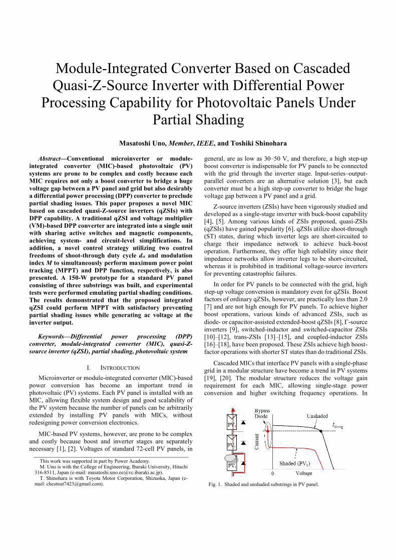
E. Extended Topology for Higher Step-Up Voltage
Conversion Ratio
The step-up ratio of the proposed qZSI is practically limited
to less than 2.0 due to limitations of duty cycle dst and
modulation index M, similar to ordinary qZSIs [7]. To achieve
higher step-up voltage conversion ratios, extended ZSI
topologies can be employed as a foundation of the proposed
integrated qZSI concept, as exemplified in Fig. 7. In this
example, a capacitor-assisted qZSI [8] is used as the foundation
that realizes twice higher voltage gain than does the basic
topology shown in Fig. 6, while the transformer is shared by the
capacitor-assisted qZSI and VM. Other extended ZSI
topologies [8]–[18] can also be employed by replacing one of
the inductors in ZSIs with a transformer. A proper topology
should be selected with considering voltage step-up
requirement and design difficulty.
Fig. 6. Proposed integrated qZSI for three substrings.
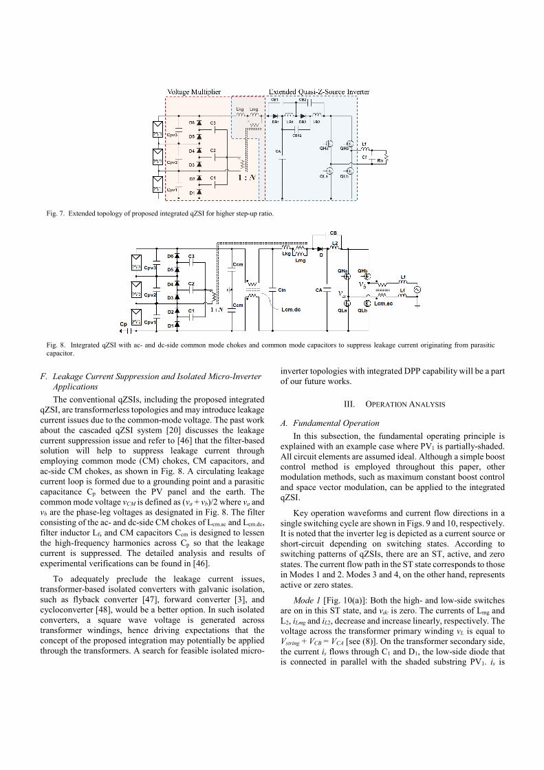
F. Leakage Current Suppression and Isolated Micro-Inverter
Applications
The conventional qZSIs, including the proposed integrated
qZSI, are transformerless topologies and may introduce leakage
current issues due to the common-mode voltage. The past work
about the cascaded qZSI system [20] discusses the leakage
current suppression issue and refer to [46] that the filter-based
solution will help to suppress leakage current through
employing common mode (CM) chokes, CM capacitors, and
ac-side CM chokes, as shown in Fig. 8. A circulating leakage
current loop is formed due to a grounding point and a parasitic
capacitance Cp between the PV panel and the earth. The
common mode voltage vCM is defined as (va + vb)/2 where va and
vb are the phase-leg voltages as designated in Fig. 8. The filter
consisting of the ac- and dc-side CM chokes of Lcm.ac and Lcm.dc,
filter inductor Lf, and CM capacitors Ccm is designed to lessen
the high-frequency harmonics across Cp so that the leakage
current is suppressed. The detailed analysis and results of
experimental verifications can be found in [46].
To adequately preclude the leakage current issues,
transformer-based isolated converters with galvanic isolation,
such as flyback converter [47], forward converter [3], and
cycloconverter [48], would be a better option. In such isolated
converters, a square wave voltage is generated across
transformer windings, hence driving expectations that the
concept of the proposed integration may potentially be applied
through the transformers. A search for feasible isolated micro-
inverter topologies with integrated DPP capability will be a part
of our future works.
III. OPERATION ANALYSIS
A. Fundamental Operation
In this subsection, the fundamental operating principle is
explained with an example case where PV1 is partially-shaded.
All circuit elements are assumed ideal. Although a simple boost
control method is employed throughout this paper, other
modulation methods, such as maximum constant boost control
and space vector modulation, can be applied to the integrated
qZSI.
Key operation waveforms and current flow directions in a
single switching cycle are shown in Figs. 9 and 10, respectively.
It is noted that the inverter leg is depicted as a current source or
short-circuit depending on switching states. According to
switching patterns of qZSIs, there are an ST, active, and zero
states. The current flow path in the ST state corresponds to those
in Modes 1 and 2. Modes 3 and 4, on the other hand, represents
active or zero states.
Mode 1 [Fig. 10(a)]: Both the high- and low-side switches
are on in this ST state, and vdc is zero. The currents of Lmg and
L2, iLmg and iL2, decrease and increase linearly, respectively. The
voltage across the transformer primary winding vL is equal to
Vstring + VCB = VCA [see (8)]. On the transformer secondary side,
the current is flows through C1 and D1, the low-side diode that
is connected in parallel with the shaded substring PV1. is is
Fig. 7. Extended topology of proposed integrated qZSI for higher step-up ratio.
Fig. 8. Integrated qZSI with ac- and dc-side common mode chokes and common mode capacitors to suppress leakage current originating from parasitic
capacitor.
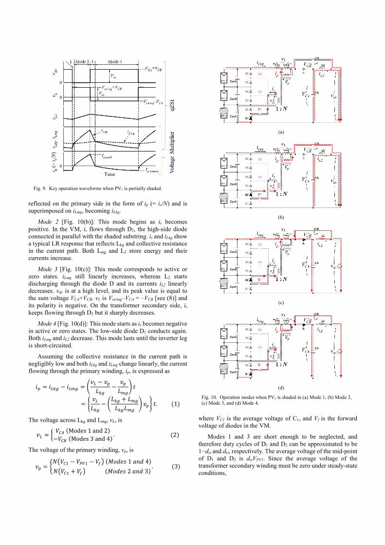
reflected on the primary side in the form of ip (= is/N) and is
superimposed on iLmg, becoming iLkg.
Mode 2 [Fig. 10(b)]: This mode begins as is becomes
positive. In the VM, is flows through D2, the high-side diode
connected in parallel with the shaded substring. is and iLkg show
a typical LR response that reflects Lkg and collective resistance
in the current path. Both Lmg and L2 store energy and their
currents increase.
Mode 3 [Fig. 10(c)]: This mode corresponds to active or
zero states. iLmg still linearly increases, whereas L2 starts
discharging through the diode D and its currents iL2 linearly
decreases. vdc is at a high level, and its peak value is equal to
the sum voltage VCA+VCB. vL is Vstring–VCA = –VCB [see (8)] and
its polarity is negative. On the transformer secondary side, is
keeps flowing through D2 but it sharply decreases.
Mode 4 [Fig. 10(d)]: This mode starts as is becomes negative
in active or zero states. The low-side diode D1 conducts again.
Both iLmg and iL2 decrease. This mode lasts until the inverter leg
is short-circuited.
Assuming the collective resistance in the current path is
negligibly low and both iLkg and iLmg change linearly, the current
flowing through the primary winding, ip, is expressed as
�� = ���� − ���� = � − ���� − ����� = � ���� − ��� + ��������� � �� . (1)
The voltage across Lkg and Lmg, vL, is
� = � ��� (Modes 1 and 2)−��" (Modes 3 and 4). (2)
The voltage of the primary winding, vp, is
� = �%&��' − �()' − �*+ (,-./0 1 12. 4)%&��' + �*+ (,-./0 2 12. 3) . (3)
where VC1 is the average voltage of C1, and Vf is the forward
voltage of diodes in the VM.
Modes 1 and 3 are short enough to be neglected, and
therefore duty cycles of D1 and D2 can be approximated to be
1−dst and dst, respectively. The average voltage of the mid-point
of D1 and D2 is dstVPV1. Since the average voltage of the
transformer secondary winding must be zero under steady-state
conditions,
Fig. 9. Key operation waveforms when PV1 is partially shaded.
(a)
(b)
(c)
(d)
Fig. 10. Operation modes when PV1 is shaded in (a) Mode 1, (b) Mode 2, (c) Mode 3, and (d) Mode 4.

��' = (1 − .34)�()' . (4)
Assuming Vf = 0 for the sake of clarity, substitution of (2)–(4)
into (1) produces the peak value of ip, Ip.peak, as
5�.�67� = ������� − % ��� + ��������� � (1 − .34)�()'� .34832 . (5)
where dst is the ST duty cycle, Ts is the switching period. From
the charge balance on C1, the bottom value of ip, Ip.bottom is
5�.:;44;� = .341 − .34 5�.�67� . (6)
In summary, vL swings and its peak-to-peak voltage is equal
to that of vdc, Vdc, as designated in Fig. 9. At the same time, a
square wave voltage with the peak-to-peak voltage of Vdc/N
appears across the secondary winding, by which the VM is
driven. In the VM, D1 and D2 that are connected in parallel with
the shaded substring PV1, are in operation, whereas others do
not conduct for the entire period, meaning only the shaded
substring receives the current from the VM. Since the average
current of C1 must be zero under steady-state conditions, the
average current of D1 or D2 is equal to the current supplied to
the shaded substring from the VM. Although the PV1-shaded
condition was taken as an example case, the VM in the proposed
integrated qZSI can operate similarly under any shading
conditions, as reported in the previous work [37].
B. Quasi-Z-Source Inverter
The operation principle of the qZSI in the proposed circuit
is essentially identical to that of traditional ones. The peak value
of the dc-link voltage vdc, Vdc, is expressed as [49]
�=> = �34?@A�1 − 2.34 = ��� + ��" , (7)
where Vstring is the string voltage. VCA and VCB are given by [19]
��� = 1 − .341 − 2.34 �34?@A�, ��" = .341 − 2.34 �34?@A� . (8)
Equation (7) suggests that, at a given value of Vdc, Vstring is
controllable and MPPT is feasible with manipulating dst.
The output peak phase voltage of the qZSI, Vo, is given by �; = ,�=> , (9)
where M is the modulation index. This equation means that the
peak dc-link voltage Vdc can be arbitrarily determined by
adjusting M at a given value of Vo. As will be discussed in detail
in the next subsection, the operation criterion of the VM in the
integrated qZSI is dependent on Vdc, and therefore M is used to
control the VM-based DPP converter.
Under unshaded conditions, no currents from the VM flow
toward substrings. The current of the secondary winding is (=
Nip) is zero, and therefore iLkg is equal to iLmg. Since the VM is
inactive under unshaded conditions, the proposed integrated
qZSI just operates as an ordinary qZSI. It suggests that, except
for the part of the VM-based DPP converter, the proposed
integrated qZSI can be designed identically to traditional ones.
Current and voltage stresses of a traditional qZSI are
summarized in [50]. Under shaded conditions, on the other hand,
the peak value of iLkg tends to be high due to the operation of
the VM-based DPP converter, as can be seen in Fig. 9. From
the derived Ip.peak (5) with the generalized current stresses of the
traditional qZSI [50], current stresses in the proposed integrated
qZSI can be determined.
C. Voltage Multiplier-Based DPP Converter
The detailed operation of the VM-based DPP converter
alone has been thoroughly analyzed in the past works [37], [38].
As discussed in Section III-A, the capacitor C1, which
corresponds to the shaded substring, is charged and discharged,
and its operation can be expressed using an equivalent
resistance.
The dc equivalent circuit of the VM-based DPP converter is
shown in Fig. 11 [37]. Req1–Req3 are equivalent resistors that
represent the charge-discharge operation of capacitors C1–C3,
and Rres is an equivalent resistance of the circuit on the primary
side. Values of Req and Rres are inversely proportional to
capacitances and switching frequency [37], [38]. The primary
winding of the ideal multi-winding transformer is connected to
the voltage source, and its value is equal to the peak-to-peak
voltage of vL. Hence, in the integrated qZSI, its value is Vdc
because the peak-to-peak voltage of vL is equal to Vdc, as
explained in Section III-A.
All the substrings are connected to the secondary winding
of the ideal multi-winding transformer through two diodes and
a respective equivalent resistor. In order for the VM to supply
equalization currents Ii (i = 13) for shaded substrings, Vdc
needs to fulfill the following relationship;
�=> > %&�() + 2�*+, (10)
where VPV is the substring voltage. From (9) and (10), the
operation criterion of the VM-based DPP converter in the
integrated qZSI is obtained as
, < �;%&�() + 2�*+. (11)
Fig. 11. DC equivalent circuit of VM-based DPP converter.

This equation suggests that the VM-based DPP converter can be
enabled/disabled by properly manipulating M depending on
partial shading conditions. When the DPP converter is enabled
by setting M low, an equalization current Ii automatically flows
toward shaded substring(s) having the lowest voltage in the string.
D. Design of Transformer and Voltage Multiplier-Based DPP
Converter
This subsection presents a design example of the
transformer as well as the VM-based DPP converter for the
proof-of-concept prototype (see Table I in Section V) with
operation constraints of dst < 0.3 and M < 1− dst for Vo = 50 V
at fs = 20 kHz. All substring voltages are assumed to be equal
to VPV = 12 V.
The transformer turns ratio N is determined from (11), as
% < �;,&�() + 2�*+ = 5.52 → 5.5, (12)
where Vf = 0.47. Since Lmg corresponds to L1 in ordinary qZSIs
[see Fig. 5(a)], the number of turns should be properly
determined to have a desired inductance value of Lmg.
As can be seen in Fig. 10, Lkg and a capacitor in the VM (i.e.,
C1 in the case of PV1-shaded condition) might resonate,
depending on operating conditions. The VM-based DPP
converter can be driven in either resonant or non-resonant mode.
The conventional VM-based DPP converter is driven with a
duty cycle of 0.5 and is suitable for resonant operations [37].
The DPP converter in the integrated qZSI, on the other hand,
operates with dst < 0.3, and the resonance leads to a higher peak
and RMS currents in the VM. However, large capacitances are
necessary to avoid the resonance, resulting in increased circuit
volume. A compromise design guideline is
2J3 > J? = 12KL���%M N@
, (13)
where Ci is the capacitance (i is the subscript number of shaded
substring). For N = 5.5 and Lkg = 7.8 H of the designed
transformer (see Table I) at fs = 20 kHz, (13) produces Ci > 61.4
F. Thus, Ci is determined to be 66 F (= 3 22 F).
IV. CONTROL STRATEGY
As mentioned in Section II-A, there are two control degrees
of freedom in qZSIs, and conventional qZSIs in energy storage
or PV applications utilize dst and M to control input and output
powers independently [49], [51]. The proposed integrated qZSI
also utilizes dst and M to realize MPPT and DPP function
simultaneously.
As mentioned in Section III-C, the operation criterion of the
DPP converter in the integrated qZSI depends on Vdc or M.
Currents for shaded substrings are supplied only when (10) is
satisfied. In other words, currents might unnecessarily flow
even under unshaded conditions if (10) is improperly fulfilled.
Therefore, Vdc should be properly regulated by adjusting M
depending on shading conditions so that currents are supplied
only for shaded substrings under shaded conditions. To this end,
Vdc needs to be higher and lower than N(VPV + 2Vf) under shaded
and unshaded conditions, respectively.
The control block diagram for the integrated qZSI is shown
in Fig. 12. It is noted that the control framework for grid
synchronization is not included for the sake of clarity. The
MPPT control is performed by adjusting dst. Meanwhile, M is
manipulated to control the VM-based DPP converter properly.
In order to supply currents only for shaded substrings under
partial shading conditions, the current sensorless ∆V-controlled
equalization strategy is employed [36]. The voltage difference
∆V between the maximum and minimum voltages among VPV1–
VPV3 is calculated and regulated to be a constant value of ∆Vref
so that only shaded substrings receive equalization currents
from the VM-based DPP converter. Under partial shading
conditions, ∆V tends to be large, and the output of the PI
controller grows, consequently reducing M. Hence, according
to (10), Vdc is controlled to be high under partial-shading
conditions. Conventional qZSIs were thoroughly analyzed to
get its transfer function [20], [49]. However, deriving a transfer
function of the VM-based DPP converter in the proposed
integrated qZSI is a daunting challenge as it operates with four
operation modes (see Figs. 9 and 10) and contains numerous
additional state variables, such as iLkg, iLmg, and voltages of C1–
C3 and Cpv1–Cpv3. Given that partial-shading conditions do not
Fig. 12. Control block diagram of V-controlled equalization and MPPT
for integrated qZSI.
(a)
(b)
Fig. 13. V-controlled equalization scenarios. (a) PV1 is shaded. (b) PV1 and PV2
are heavily- and lightly-shaded.

change rapidly, PI parameters for the V-controlled
equalization loop are determined with trial-and-error basis so
that its gain in a high-frequency region can be low enough to
ensure the stability.
Images of the ∆V-controlled equalization strategy are
illustrated in Fig. 13. Figure 13(a) deals with the case that PV1
is partially-shaded. The operating point of the unshaded
substrings, PV2 and PV3, is determined to be at point A, the
intersection point of Istring and characteristics of PV2 and PV3.
Meanwhile, since ∆V is controlled to be a certain fixed value,
the operating point of the shaded substrings PV1 must be V
lower than point A. The operating point of PV1 must be on the
dashed line L and is determined to be B. The current difference
between A and B corresponds to I1 (i.e., a current supplied to
the shaded substring from the VM). Although substring
voltages cannot be completely equalized, the shaded substring
PV1 can operate at near its MPP by setting ∆V as low as possible.
The substring voltages in the case of Fig. 13(a) are given by
��()' = �3 − 2�* − 5'O6P�()M = �()Q ≥ �3 − 2�* , (14)
where Req is the equivalent resistance, and Vs is the secondary
winding voltage. The combination of these two equations
produces the voltage difference V between the shaded and
unshaded substrings ∆� = �()Q − �()' ≥ 5'O6P . (15)
This equation suggests that the value of Vref needs to be
determined with considering Req and the largest expected
equalization current under partial shading conditions. To
minimize the voltage difference and to satisfactorily equalize
substring voltages, Vref should be set to be as small as possible
with ensuring a margin for noise and double-line frequency
ripples. If this equation is violated, currents unnecessarily flow
toward unshaded substrings, resulting in increased processing
power as well as losses in the VM. The value of V for the ∆V-
controlled equalization strategy will be determined from the
experimentally-obtained Req (see Section V-B).
Figure 13(b) illustrates the case that PV1 and PV2 are
heavily- and lightly-shaded condition. Both PV1 and PV2
receive currents from the DPP converter. The current supplied
to PV1, I1, is larger than that for PV2, I2, causing a larger voltage
drop across Req for PV1 in the form of I1Req. Therefore, the
voltage of the heavily shaded PV1, VPV1, tends to be lower than
VPV2 because of the larger voltage drop. The voltage difference
∆V between the maximum and minimum voltages in this case
is VPV3 – VPV1, and therefore the operating point of PV1 must be
V lower than point A and is determined to be B. VPV2 is
between VPV1 and VPV3, and the operating point of PV2 is at C.
The substring voltages in the case of Fig. 13(b) are
expressed as
T�()' = �U − 2�* − 5'O6P�()M = �U − 2�* − 5MO6P�()Q ≥ �U − 2�*. (16)
Since ∆V in the case of Fig. 13(b) is VPV3 – VPV1, the
rearrangement of (16) produces an equation identical to (15).
This fact suggests that the V-controlled strategy can equalize
all the substring voltages with an error of V, regardless of
shading conditions.
V. EXPERIMENTAL RESULTS
A. Prototype
The operation of the proposed integrated qZSI was verified
using the prototype for a standard 72-cell PV panel comprising
three substrings. The prototype and its component values are
shown in Fig. 14 and Table I. PV MICs are often installed on
the back of PV panels, and the proposed integrated qZSI would
be installed similarly. This prototype, however, was designed
for proof-of-concept, not for practical use. Bulky high-profile
components, such as the transformer with an RM14 core,
should preferably be replaced with low-profile ones for the
integrated qZSI to be installed on the back of PV panels.
TMS320F28335 control card (Texas Instruments) was used for
the MPPT and V-controlled equalization. The prototype operated
Table I. Component values used for the prototype.
Component Value
Cext
Aluminum Electrolyt ic Capacitor, 330 μF 6
CA, C
BAluminum Electrolytic Capacitor, 1 mF 4
L2
150 μH
Switches BSC320N20NS3, Ron
= 32 mΩ
Diode Fast Recovery Diode, BVY29, VF = 1.05 V
Transformer N1:N
2 = 22:4, L
kg = 7.8 μH, L
mg = 263 μH
C1–C
3Ceramic Capacitor, 22 μF × 3
Cpv1
–Cpv3
Ceramic Capacitor, 47 μF × 4
D1–D
4Schottky Barrier Diode, SL42, V
F = 0.47 V
Gate Driver IRS2186
Fig. 14. 150-W prototype of proposed integrated qZSI.
Fig. 15. Experimental setup to measure output characteristics of VM-
based DPP converter.

at a switching frequency of 20 kHz. The measured power
conversion efficiency under an unshaded condition with Vstring = 36
V was 83–90% in the output power range of 50–160 W.
B. Output Characteristics of VM-Based DPP Converter
The output characteristics of the VM in the integrated qZSI
was measured using the experimental setup shown in Fig. 15.
Substrings were removed, and an external power supply Vext of
36 V was connected to the input. By directly connecting the
variable resistor Rvar to Cpv1, the current-flow-path under the
PV1-shaded condition (see Fig. 10) can be emulated. The output
current IRvar and the voltage across Cpv1, VPV1, were measured
with manually regulating Vdc to be 52, 60, 72, or 90 V. M was
fixed to be 0.78, and a load resistance Ro of 100 was
connected to the output of the inverter.
The measured output characteristic of the VM-based DPP
converter is shown in Fig. 16. VPV1 almost linearly decreased
with IRvar. Slopes of the measured characteristics were
independent on Vdc, and Req was determined to be 0.60 .
C. String Characteristics under Partial Shading Condition
A partial shading condition was mimicked using solar array
simulators (E4361A, Keysight Technologies). Individual
substring characteristics used for the experiments are shown in
Fig. 17(a). PV2 and PV3 were unshaded, while PV1 was shaded.
The string power available in the ideal case under this partial
shading condition was 141.2 W (= 27.2 W + 57.0 W 2). The
current difference between the shaded and unshaded substrings
was approximately 2.0 A in this case, and Req was determined
to be 0.60 from the measured characteristics of the VM (see
Fig. 16). Accordingly, ∆Vref for the current sensorless
equalization was set to be 2.0 V to fulfill (15) with considering
the influence of noise and leaving enough margin. M was
manipulated to achieve ∆V-controlled equalization, while dst
was fixed to be 0.2 and the load resistance Ro was manually
varied in order to sweep the string characteristics.
Fig. 16. Measured output characteristics of VM-based DPP converter.
16
14
12
10
8
6
4
Vo
ltag
e V
PV
1 [
V]
3.02.01.00.0
Current IRvar [A]
Vdc = 90 V
72 V
60 V
52 V
Req = 0.60
(a)
(b)
Fig. 18. Measured waveforms at string’s MPP. (a) Key waveforms. (b) vo and vdc.
100806040200
v dc
[V]
6040200
-20-40
v p [
V]
1086420
i Lkg
[A
]
20
10
0
-10
i s [A
]
Time [5 s/div]
543210
i L2 [
A]
-80
-40
0
40
80
v o [
V]
10080604020
0
vdc
[V]
Time [5 ms/div]
(a)
(b)
Fig. 17. (a) Substring characteristics, (b) string characteristics with/without
DPP function.
6
5
4
3
2
1
0
Curr
ent
[A]
20151050Substring Voltage, VPVi [V]
60
40
20
0
Pow
er [
W]
PV1
PV2, PV3
(11.0, 2.47)
(12.8, 4.45)
PV1
PV2, PV3(12.8, 57.0)
(11.0, 27.2)
140
120
100
80
60
40
20
0
Outp
ut
Pow
er [
W]
50403020100
String Voltage, Vstring [V]
w/ DPPw/o DPP
113 W
87.0 W

The measured inverter output power characteristics as a
function of string voltage with/without the DPP function are
shown and compared in Fig. 17(b). In the case without the DPP
function, the secondary winding was opened to disable the
operation of the VM. Without the DPP converter, two power
point maxima (a local and global MPPs) were observed, and the
maximum power available at the inverter output was merely 87.0
W at Vstring = 25.5 V. With the DPP function of the integrated
qZSI, on the other hand, the local MPP disappeared, and the
maximum output power increased to as high as 113 W at Vstring =
36.7 V. The available power at the inverter output increased by
30%, and 80% of the ideal string power (= 113 W/141.2 W) could
be delivered to the output port. Given that the power conversion
efficiency of the prototype was 83–90% in the range of 50–160
W, the string was utilized well even under this partial shading
condition, demonstrating the DPP function of the integrated qZSI.
At Vstring = 36.7 V with dst = 0.2, Vdc, VCA, and VCB were measured
to be 61.6, 48.7, and 12.0 V, respectively, agreeing well with the
theoretical values of (7) and (8).
The measured key operation waveforms at the string’s
maximum power point of Vstring = 36.7 V are shown in Fig. 18(a).
These waveforms matched well with the theoretical ones shown
in Fig. 8. The measured vo and vdc are shown in Fig. 18(b). vdc
swung while generating ac voltage with an RMS value of 36 V.
These results demonstrated that the proposed integrated qZSI
can produce ac output voltage with precluding the negative
issues of partial shading.
D. MPPT under Partial Shading Condition
The experimental MPPT test employing the proposed
control strategy was performed emulating a partial shading
condition. From the experimentally obtained Req of 0.60 (see
Fig. 16), Vref was determined to be 2.0 V for an equalization
current of 1.0 A with considering a margin for noise and double-
line frequency ripple. V of substring voltages was regulated to
be 2.0 V by manipulating M, while the MPP of the string was
tracked using the hill climbing algorithm with a duty cycle
perturbation dst of 0.2%. The sampling interval for the MPPT
was set to be 2.0 s, which is hundred times greater than the line
frequency period of 20 ms, so that the MPPT operation is not
affected by the line frequency of 50 Hz. The key parameters of
substring characteristics used for the MPPT test are listed in
Table II. The maximum powers of shaded and unshaded
substrings were 10.5 and 23.6 W, respectively, and the available
maximum string power was 57.7 W in this condition.
The experimental results are shown in Fig. 19. The voltage
difference between the shaded and unshaded substrings was
controlled to be about 2.0 V, though substring voltages fluctuated
due to the duty cycle perturbation. The extracted power reached
around 57.0 W after the operation came to the steady state,
demonstrating the integrated functions of the MPPT and
preclusion of decreased power yield by partial shading.
VI. SYSTEM EFFICIENCY COMPARISON
As depicted in Fig. 3, PV systems consist of multiple
converters and therefore should be evaluated and compared
based on system efficiencies, not converter efficiencies alone.
This section presents the comparison between the proposed
integrated qZSI system and several representative conventional
DPP converters for PV panels comprising three substrings, as
shown in Table III. DPP converter efficiencies are a power
conversion efficiency of a DPP converter alone. Irradiance
Fig. 19. Experimental results of MPPT with ∆V control.
16
12
8
4VP
V1–V
PV
3 [
V]
250200150100500
Time [s]
80
60
40
20
0
Pow
er [
W]
100806040200
Vdc
[V]
VPV1VPV2, VPV3
2.0 V
Table II. Key parameters of substring characteristics in MPPT test.
V mp [V] V oc [V] I mp [A] I sc [A] P MPP [W]
PV1 (Shaded) 11 14 0.95 1.0 10.5
PV2, PV3 (Unshaded) 12.4 16 1.9 2.0 23.6
Table III. System efficiency comparison.
Topology Architecture ControlDPP Converter
Efficiency
Irradiance
Condition
Extraction
Efficiency
System
Efficiency
Resonant SCC
[30]
Adjacent Substring
[Fig. 2(a)]
Voltage
Equalization99% 100%, 100%, 60% 98.0% 84.3%
Multi-Stacked Buck-
Boost Converter [35]
String-to-substring
[Fig. 2(b)]
Voltage
Equalization90% 100%, 66%, 33% 91.6% 78.8%
Flyback Converter
[39]
String-to-substring
[Fig. 2(c)]
Voltage
Equalization90% 100%, 100%, 60% 96.3% 82.8%
Flyback Converter
[41]
Substring-to-IP
[Fig. 2(e)]dMPPT 94% 100%, 100%, 50% 98.0% 84.3%
Flyback Converter
[42]
Substring-to-IP
[Fig. 2(e)]
Voltage
EqualizationNot Reported 100%, 75%, 50% 96.5% 83.0%
ProposedIntegrated qZSI
(Fig. 4)
Voltage
EqualizationN/A 100%, 100%, 60% N/A 80.0%

conditions represent relative values of short-circuit currents or
maximum powers of individual three substrings. The extraction
efficiency is defined as a ratio of an extracted power to an ideal
panel power under partial shading conditions. System
efficiencies were determined with a premise that a qZSI with a
power conversion efficiency of 86% was employed for all
conventional DPP systems—the 86%-efficiency was
equivalent to the measured efficiency of the proposed
integrated qZSI under unshaded conditions.
Extraction efficiencies of conventional DPP systems are
reportedly higher than 90%, depending on topologies and
irradiance conditions, and their system efficiencies are around
83%. Meanwhile, the measured system efficiency of the
proposed integrated qZSI is 80% (see Section V-C). The
inferior system efficiency is chiefly attributable to that the
individual performances as a qZSI and DPP converter cannot
be optimized due to the integration, as discussed in Section II-
C. Furthermore, with the ∆V-controlled equalization strategy,
the residual voltage difference ∆V remains even with the DPP
function, impairing the system efficiency. Thus, the proposed
integrated qZSI is considered better suitable for applications
where the system simplification and cost reduction are
prioritized over system efficiency enhancement, as mentioned
in Section II-C.
VII. CONCLUSION
A novel PV MIC based on cascaded qZSI with DPP
capability has been proposed in this paper. The proposed qZSI
can be derived by integrating a traditional qZSI and VM-based
DPP converter into a single unit with sharing active switches
and magnetic components, realizing the simplified system and
circuit. The operational analysis revealed that two control
freedoms of shoot-through duty cycle dst and modulation index
M can be utilized to simultaneously perform the MPPT and
DPP function, respectively.
The control strategy for the integrated qZSI has also been
presented. MPPT is performed by adjusting dst, while M is
manipulated based on the V-controlled equalization strategy,
with which a voltage difference between shaded and unshaded
substrings is controlled to be a certain fixed value so that partial
shading issues are prevented by the DPP converter.
The 150-W prototype of the integrated qZSI was built for a
standard 72-cell PV panel comprising three substrings.
Experimental tests were performed emulating partial shading
conditions. The extractable maximum power from the partially-
shaded panel increased by 30% under a certain condition,
demonstrating the DPP function of the integrated qZSI. With
the proposed control strategy, the MPP was properly tracked
with regulating V to be a fixed value, demonstrating the
integrated functions of MPPT and DPP.
REFERENCES
[1] D. Leuenberger and J. Biela, “PV-module-integrated AC inverter (AC module) with subpanel MPP tracking,” IEEE Trans. Power Electron.,
vol. 32, no. 8, pp. 6105–6118, Aug. 2017.
[2] C.Y. Liao, W.S. Lin, Y.M. Chen, and C.Y. Chou, “A PV micro-inverter
with PV current decoupling strategy,” IEEE Trans. Power Electron., vol.
32, no. 8, pp. 6544–6557, Aug. 2017. [3] D. Meneses, O. Garcia, P. Alou, J.A. Oliver, and J.A. Cobos, “Grid-
connected forward microinverter with primary-parallel secondary-series
transformer,” IEEE Trans. Power Electron., vol. 30, no. 9, pp. 4819–4830, Sep. 2015.
[4] F.Z. Peng, “Z source inverter,” IEEE Trans. Ind. Appl., vol. 39, no. 2, pp.
504–510, Mar./Apr. 2003. [5] Y. Huang, M. Shen, F.Z. Peng, and J. Wang, “Z-source inverter for
residential photovoltaic systems,” IEEE Trans. Power Electron., vol. 21,
no. 6, pp. 1776–1782, Nov. 2006. [6] O. Husev, F. Blaabjerg, C.R. Clemente, E.R. Cadaval, D. Vinnikov, Y.P.
Siwakoti, and R. Strzelecki, “Comparison of impedance-source networks
for two and multilevel buck–boost inverter applications,” IEEE Trans. Power Electron., vol. 31, no. 11, pp. 7564–7579, Nov. 2016.
[7] M. Hanif, M. Basu, and K. Gaughan, “Understanding the operation of a
Z-source inverter for photovoltaic application with a design example,” IET Power Electron., vol. 4, no. 3, pp. 278–287, Mar. 2009.
[8] C. J. Gajanayake, F. L. Luo, H.B. Gooi, P.L. So and L.K. Siow,
“Extended-boost Z-Source inverters,” IEEE Trans. Power Electron., vol. 25, no. 10, pp. 2642–2652, Oct. 2010.
[9] W. Mo, P.C. Loh, and F. Blaabjerg, “Asymmetrical -source inverters,”
IEEE Trans. Ind. Electron., vol.61, no. 2, pp. 637–647, Feb. 2014. [10] M. Zhu, K. Yu, and F.L. Luo, “Switched inductor Z-source inverter,”
IEEE Trans. Power Electron., vol. 25, no. 8, pp. 2150–2158, Aug. 2010.
[11] D. Li, P.C. Loh, M. Zhu, F. Gao, and F. Blaabjerg, “Generalized multicell switched-inductor and switched-capacitor Z-source inverters,”
IEEE Trans. Power Electron., vol. 28, no. 2, pp. 837–848, Feb. 2013.
[12] A.V. Ho, T.W. Chun, and H.G. Kim, “Extended boost active-switched-capacitor/switched-inductor quasi-Z-source inverters,” IEEE Trans.
Power Electron., vol. 30, no. 10, pp. 5681–5690, Oct. 2015.
[13] W. Qian, F.Z. Peng and H. Cha, “Trans-Z-source inverters,” IEEE Trans. Power Electron., vol. 26, no. 12, pp. 3453–3463, Dec. 2011.
[14] M.K. Nguen, Y.C. Lim, and S.J. Park, “Improved trans-Z-source inverter with continuous input current and boost inversion capability,” IEEE Trans. Power Electron., vol. 28, no. 10, pp. 4500–4510, Oct. 2013.
[15] M.K. Nguen, Y.C. Lim, and Y.G. Kim, “TZ-source inverters,” IEEE Trans. Ind. Electron., vol.60, no. 12, pp. 5686–5695, Dec. 2013.
[16] P.C. Loh and F. Blaabjerg, “Magnetically coupled impedance-source
inverters,” IEEE Trans. Ind. Appl., vol. 49, no. 5, pp. 2177–2187, Sep./Oct. 2013.
[17] Y. Zhou and W. Huang, “Single-stage boost inverter with coupled
inductor,” IEEE Trans. Power Electron., vol. 27, no. 4, pp. 1885–1893, Apr. 2012.
[18] S.S. Nag and S. Mishra, “A coupled inductor based high boost inverter
with sub-unity turns-ratio range,” IEEE Trans. Power Electron., vol. 31, no. 11, pp. 7534–7543, Nov. 2016.
[19] Y. Zhou, L. Liu, and H. Li, “A high-performance photovoltaic module-
integrated converter (MIC) based on cascaded quasi-Z-source inverters (qZSI) using eGaN FETs,” IEEE Trans. Power Electron., vol. 28, no. 6,
pp. 2727–2738, Jun. 2013.
[20] D. Sun, B. Ge, W. Liang, H. Abu-Rub, and F.Z. Peng, “An energy stored quasi-Z-source cascade multilevel inverter-based photovoltaic power
generation system,” IEEE Trans. Ind. Electron., vol. 62, no. 9, pp. 5458–
5467, Sep. 2015. [21] S.M. MacAlpine, R.W. Erickson, and M.J. Brandemuehl,
“Characterization of power optimizer potential to increase energy capture in photovoltaic systems operating under nonuniform conditions,” IEEE Trans. Power Electron., vol. 28, no. 6, pp. 2936–2945, Jun. 2013.
[22] H. Jeong, H. Lee, Y.C. Liu, and K.A. Kim, “Review of differential power
processing converters techniques for photovoltaic applications,” IEEE Trans. Energy Conversion, to be published.
[23] H.J. Bergveld, D. Büthker, C. Castello, T. Doorn, A.D. Jong, R.V. Otten,
and K.D. Waal, “Module-level dc/dc conversion for photovoltaic systems: the delta-conversion concept,” IEEE Trans. Power Electron.,
vol. 28, no. 4, pp. 2005–2013, Apr. 2013.
[24] M.S. Zaman, Y. Wen, R. Fernandes, B. Buter, T. Doorn, M. Dijkstra, H.J. Bergveld, and O. Trescases, “A cell-level differential power processing
IC for concentrating-PV systems with bidirectional hysteretic current-
mode control and closed-loop frequency regulation,” IEEE Trans. Power Electron., vol. 30, no. 12, pp. 7230–7244, Dec. 2015.

[25] P.S. Shenoy, K.A. Kim, B.B. Johnson, and P.T. Krein, “Differential
power processing for increased energy production and reliability of
photovoltaic systems,” IEEE Trans. Ind. Power Electron., vol. 28, no. 6, pp. 2968–2979, Jun. 2013.
[26] S. Qin, S.T. Cady, A.D.D. García, and R.C.N.P. Podgurski, “A
distributed approach to maximum power point tracking for photovoltaic submodule differential power processing,” IEEE Trans. Power Electron.,
vol. 30, no. 4, pp. 2024–2040, Apr. 2015.
[27] S. Qin, C.B. Barth, and R.C.N.P. Podgurski, “Enhancing microinverter energy capture with submodule differential power processing,” IEEE
Trans. Power Electron., vol. 31, no. 5, pp. 3575–3585, May 2016.
[28] T. Shimizu, O, Hashimoto, and G. Kimura, “A novel high-performance utility-interactive photovoltaic inverter system,” IEEE Trans. Power Electron., vol. 18, no. 2, pp. 704–711, Mar. 2003.
[29] T. Shimizu, M. Hirakata, T. Kamezawa, and H. Watanabe, “Generation control circuit for photovoltaic modules,” IEEE Trans. Power Electron.,
vol. 16, no. 3, pp. 293–300, May 2001.
[30] J.T. Stauth, M.D. Seeman, and K. Kesarwani, “Resonant switched-capacitor converters for sub-module distributed photovoltaic power
management,” IEEE Trans. Power Electron., vol. 28, no. 3, pp. 1189–
1198, Mar. 2013. [31] P.K. Peter and V. Agarwal, “Current equalization in photovoltaic strings
with module integrated ground-isolated switched capacitor DC–DC
converters,” IEEE J. Photovoltaics., vol. 4, no. 2, pp. 669–678, Mar. 2014. [32] A. Blumenfeld, A. Cervera, and M.M. Peretz, “Enhanced differential
power processor for PV systems: resonant switched-capacitor gyrator
converter with local MPPT,” IEEE J. Emerging Selected Topics in Power Electron., vol. 2, no. 4, pp. 883–892, Dec. 2014.
[33] M. Uno and A. Kukita, “PWM converter integrating switched capacitor
converter and series-resonant voltage multiplier as equalizers for photovoltaic modules and series-connected energy storage cells for
exploration rovers,” IEEE Trans. Power Electron., vol. 32, no. 11, pp.
8500–8513, Nov. 2017. [34] J. Du, R. Xu, X. Chen, Y. Li, and J. Wu, “A novel solar panel optimizer
with self-compensation for partial shadow condition,” in Proc. IEEE Applied Power Electron. Conf. Expo., APEC, pp. 92–96, 2013.
[35] M. Uno and A. Kukita, “Single-switch voltage equalizer using multi-
stacked buck-boost converters for partially-shaded photovoltaic modules,” IEEE Trans. Power Electron., vol. 30, no. 6, pp. 3091–3105,
Jun. 2015.
[36] M. Uno and A. Kukita, “Current sensorless equalization strategy for a single-switch voltage equalizer using multistacked buck–boost
converters for photovoltaic modules under partial shading,” IEEE Trans.
Ind. Appl., vol. 53, no. 1, pp. 420–429, Jan./Feb. 2017. [37] M. Uno and A. Kukita, “Two-switch voltage equalizer using an LLC
resonant inverter and voltage multiplier for partially-shaded series-
connected photovoltaic modules,” IEEE Trans. Ind. Appl., vol. 51, no. 2, pp. 1587–1601, Mar./Apr. 2015.
[38] M. Uno and A. Kukita, “Single-switch single-magnetic PWM converter
integrating voltage equalizer for partially-shaded photovoltaic modules in standalone applications,” IEEE Trans. Power Electron., vol. 33, no. 2,
pp. 1259–1270, Feb. 2018.
[39] C. Olalla, D. Clement, M. Rodríguez, and D. Makisimović, “Architectures and control of submodule integrated dc-dc converters for
photovoltaic applications,” IEEE Trans. Power Electron., vol. 28, no. 6,
pp. 2980–2997, Jun. 2013. [40] C. Olalla, C. Deline, D. Clement, Y. Levron, M. Rodríguez, and D.
Makisimović, “Performance of power limited differential power
processing architectures in mismatched PV systems,” IEEE Trans. Power Electron., vol. 30, no. 2, pp. 618–631, Feb. 2015.
[41] R. Bell and R.C.N.P. Podgurski, “Decoupled and distributed maximum
power point tracking of series-connected photovoltaic submodules using
differential power processing,” IEEE J. Emerging Selected Topics in
Power Electron., vol. 3, no. 4, pp. 881–891, Dec. 2015.
[42] Y. Levron, D.R. Clement, B. Choi, C. Olalla, and D. Maksimovic, “Control of submodule integrated converters in the isolated-port
differential power-processing photovoltaic architecture,” IEEE J.
Emerging Selected Topics in Power Electron., vol. 2, no. 4, pp. 821–832, Dec. 2014.
[43] G. Chu, H. Wen, L. Jiang, Y. Hu, and X. Li, “Bidirectional flyback based
isolated-port submodule differential power processing optimizer for photovoltaic applications,” Solar Energy, vol. 158, pp. 929–940, Oct. 2017.
[44] Y.T. Jeon, H. Lee, K.A. Kim, and J.H. Park, “Least power point tracking
method for photovoltaic differential power processing systems,” IEEE Trans. Power Electron., vol. 32, no. 3, pp. 1941–1951, Mar. 2017.
[45] T. Shinohara and M. Uno, “Micro-inverter based on quasi-Z-source
inverter integrating switchless voltage equalizer for photovoltaic panels under partial shading,” in Proc. Int. Future Energy Electron. Conf.
(IFEEC), ECCE-Asia, pp. 2013–2018, Jun. 2017.
[46] Y. Zhou and H. Li, “Analysis and suppression of leakage current in cascaded-multilevel-inverter-based PV systems,” IEEE Trans. Power
Electron., vol. 29, no. 10, pp. 5265–5277, Oct. 2014.
[47] J. Kan, Y. Wu, L. Qin, and S. Luo, “Integrated double dual-Mosfets photovoltaic micro-inverter with current-source characteristic,” in Proc. Int.
Future Energy Electron. Conf. (IFEEC) ECCE-Asia, pp. 134–139 2017.
[48] D.R. Nayanasiri, D.M. Vilathgamuwa, and D.L. Maskell, “Half-wave cycloconverter-based photovoltaic microinverter topology with phase-
shift power modulation,” IEEE Trans. Power Electron., vol. 28, no. 6,
pp. 2700–2710, Jun. 2013. [49] B. Ge, H. Abu-Rub, F.Z. Peng, Q. Lei, A.T. Almeida, F.J.T.E. Ferreira,
D. Sun, and Y. Liu, “An energy-stored quasi-Z-source inverter for
application to photovoltaic power system,” IEEE Trans. Ind. Electron., vol. 60, no. 10, pp. 4468–4481, Oct. 2013.
[50] M.K. Nguyen, Y.C. Lim, and S.J. Park, “A comparison between single-
phase quasi-Z-source and quasi-switched boost inverters,” IEEE Trans. Ind. Electron., vol. 62, no. 10, pp. 6336–6344, Oct. 2015.
[51] F.Z. Peng, M. Shen, and K. Holland, “Applications of Z-source inverter for traction drive of fuel cell—battery hybrid electric vehicles,” IEEE
Trans. Power Electron., vol. 22, no. 3, pp. 1054–1061, May 2007.
Masatoshi Uno (M’06) was born in Japan in 1979. He received the B.E. degree in electronics
engineering and the M.E. degree in electrical
engineering from Doshisha University, Kyoto, Japan, and the Ph.D. degree in space and astronautical
science from the Graduate University for Advanced
Studies, Hayama, Japan, in 2002, 2004, and 2012, respectively.
In 2004, he joined the Japan Aerospace Exploration
Agency, Sagamihara, Japan, where he developed spacecraft power systems including battery, photovoltaic, and fuel cell systems.
In 2014, he joined the Department of Electrical and Electronics Engineering,
Ibaraki University, Ibaraki, Japan, where he is currently an Associate Professor of Electrical Engineering.
His research interests include switching power converters for renewable
energy systems, life evaluation for EDLCs and lithium-ion batteries, and development of spacecraft power systems. Dr. Uno received the Isao Takahashi Power Electronics Award in 2018.
Toshiki Shinohara was born in 1992. He received
the B.E. and M.S. degrees in electrical and
electronics engineering from Ibaraki University, Ibaraki, Japan in 2016 and 2018, respectively. He is
currently with TOYOTA corporation. His research
interests include dc-dc converters and inverters for
photovoltaic systems.
Related Documents


![An Efficient Bridge-Less Power Factor Correction Tapped ... · Cuk converter topology is generally a converter with lesser efficiency, ... TI-flyback [12], TI-cascaded boost [12];](https://static.cupdf.com/doc/110x72/5b019fb47f8b9a84338e6c9c/an-efficient-bridge-less-power-factor-correction-tapped-converter-topology-is.jpg)


