MODULE I PROCESS STEPS IN IC FABRICATION INTRODUCTION The monolithic IC is one in which all circuit components are fabricated into or top of a block of silicon which is referred to as chip (or dies). Interconnections between the components within the chip are made by means of metallization patterns, and the individual components are not separable from the circuit. The processing steps used to fabricate various silicon devices, such as diodes, transistors, and integrated circuits are as follows: 1. Refining and growth of Silicon Crystals 2. Si Wafer preparation 3. Diffusion (and ion implantation) of dopant impurities 4. Oxidation 5. Photolithography 6. Chemical vapour deposition (including epitaxy) 7. Metallization. 8. Testing and chip separation 9. Packaging The fabrication of devices starts with single-crystal silicon wafers. Then the processes listed above can be used to produce discrete devices (i.e., individual diodes and transistors) and ICs. These devices or ICs will be in wafer form with tens, hundreds, or even thousands of discrete devices or ICs on the same silicon wafer. The wafer is then divided up to obtain the individual dice or chips. These chips are then encapsulated or packaged, with a wide variety of packages and packaging methods being possible.

Welcome message from author
This document is posted to help you gain knowledge. Please leave a comment to let me know what you think about it! Share it to your friends and learn new things together.
Transcript

MODULE I
PROCESS STEPS IN IC FABRICATION
INTRODUCTION
The monolithic IC is one in which all circuit components are fabricated into or top of a block of silicon
which is referred to as chip (or dies). Interconnections between the components within the chip
are made by means of metallization patterns, and the individual components are not separable
from the circuit.
The processing steps used to fabricate various silicon devices, such as diodes, transistors, and integrated
circuits are as follows:
1. Refining and growth of Silicon Crystals
2. Si Wafer preparation
3. Diffusion (and ion implantation) of dopant impurities
4. Oxidation
5. Photolithography
6. Chemical vapour deposition (including epitaxy)
7. Metallization.
8. Testing and chip separation
9. Packaging
The fabrication of devices starts with single-crystal silicon wafers. Then the processes listed above can
be used to produce discrete devices (i.e., individual diodes and transistors) and ICs. These devices or
ICs will be in wafer form with tens, hundreds, or even thousands of discrete devices or ICs on the same
silicon wafer. The wafer is then divided up to obtain the individual dice or chips. These chips are then
encapsulated or packaged, with a wide variety of packages and packaging methods being possible.
Packaging provides
encapsulation of the chip for protection of the environmental effects, and
Easy access to the various parts of the chip by means of a lead or pin structure such that
the device may be conveniently plugged into or attached to the rest of the system.
The process steps for wafer fabrication are generally applied a number of times in succession, especially
in the case of ICs, where as many as 10 repetitions of the photolithography, oxidation, and
diffusion steps may be used.

REFINING AND GROWTH OF SILICON CRYSTALS
The most commonly available natural sources of silicon are silica and silicates. At present, silicon-made
devices constitute over 95% of all semiconductor devices.
The reasons for using silicon as a suitable material for IC fabrication are:
1. Silicon devices can operate up to 150˚C versus 100˚C for Germanium.
2. Silicon grows a stable oxide (SiO2), which is one of the very important process steps in the
fabrication of ICs. Germanium oxides are unsuited for devices applications.
3. The intrinsic (Undoped) resistivity of Ge is about 47Ω-cm, which precludes the fabrication of
rectifying devices with high breakdown voltages. The intrinsic resistivity of Si is 23x104Ω-cm,
thus high rectifying devices are practical with Si.
4. Electronic graded Ge is more costly than Si.
Production of Electronic Grade Silicon (EGS)
The raw material for the preparation of single-crystal silicon is the electronic-grade silicon (EGS) which
is a polycrystalline material of high purity. The major impurities in the EGS are boron, carbon, and
residual donors. Pure EGS should have doping elements in the parts per billion (ppb) range, and carbon
less than, 2 parts per million (ppm). Production of EGS is a multistep process as shown in Fig.1.
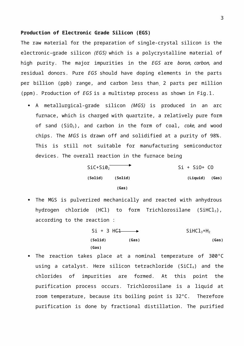
A metallurgical-grade silicon (MGS) is produced in an arc furnace, which is charged with
quartzite, a relatively pure form of sand (SiO2), and carbon in the form of coal, coke, and wood
chips. The MGS is drawn off and solidified at a purity of 98%. This is still not suitable for
manufacturing semiconductor devices. The overall reaction in the furnace being
SiC+Si02 Si + SiO+ CO
(Solid) (Solid) (Liquid) (Gas) (Gas)
The MGS is pulverized mechanically and reacted with anhydrous hydrogen chloride (HCl) to
form Trichlorosilane (SiHCl3), according to the reaction :
Si + 3 HC1 SiHCl3+H2
(Solid) (Gas) (Gas) (Gas)
The reaction takes place at a nominal temperature of 300°C using a catalyst. Here silicon
tetrachloride (SiCI4) and the chlorides of impurities are formed. At this point the purification
process occurs. Trichlorosilane is a liquid at room temperature, because its boiling point is
32°C. Therefore purification is done by fractional distillation. The purified SiHCl3 is subjected
to chemical vapour deposition (CVD) to be discussed later. The chemical reaction is a
hydrogen reduction of SiHCl3.
2
2SiHC13+ 2H2 2Si+ 6HCl
The reaction takes place in a CVD reactor in which a resistance-heated Si-rod (4-mm diameter),
called a "slim-rod", serves as the nucleation point for the deposition of silicon. The process results in
rods of EGS which are up to 0.2 m (or more) in diameter and several meters in length. EGS can be cut
from these rods as single chunks or crushed into nuggets. To achieve high overall efficiency of the
process, feedback or recycling of reaction byproducts is used as shown in Fig.1.
There is also another process of producing EGS in which silane (SiH4) is subjected to
pyrolysis.
SiH4+heat Si + 2H2
(Gas) (Solid) (Gas)
In this process the CVD reactor is operated at about 900°C and supplied with silane instead of
Trichlorosilane. The advantages of producing EGS from silane are lower cost and less harmful
reaction byproducts.
Crystal Structure and Growing
3

Crystal structure: Though EGS is highly refined, it is not suitable for manufacturing ICs because IC
components are formed in a single crystal silicon wafer. The silicon wafer must be single crystal, but it
does not represent an ideal crystal due to following reasons:
The wafer has finite boundaries; thus, atoms at the surfaces are incompletely bonded as against
those in the bulk of the wafer material.
The atoms are displaced from their ideal locations by thermal agitation.
Real crystals have defects which are mainly classified into four types :
o point defect,
o line defect (dislocation),
o area or planar defect, and
o Volume defect.
The crystal defects influence the optical, electrical, and mechanical properties of silicon.
Point defect refers to following forms of defect:
A nonsilicon atom incorporated into the lattice at either a substitutional or interstitial site: The
former refers to site produced by replacing a parent silicon atom and the latter refers to existing
site between silicon atoms. The nonsilicon atom may be an intentional dopant as introduced
by diffusion process (to be discussed) or an unintentional impurity.
A vacancy in the lattice created due to missing atom: this is also known as a Schottky defect.
A silicon atom in an interstitial lattice site with an associated vacancy: this is also known as a
Frenkel defect.
Chemicalvapour deposition (including epitaxy)
Metallization
Vacancies and interstitials have equilibrium concentrations that depend on temperature. Point defects
are important in the kinetics of diffusion and oxidation. The diffusion of many impurities depends on
the vacancy concentration, as does the oxidation rate of silicon.
Dislocations second class of defects. There may be edge (line) dislocation or screw dislocation. The
edge dislocation in a cubic lattice may be created by an extra plane of atoms. Crystals for IC usage
are generally grown free of edge dislocations, but may contain small dislocation loops from excess
point-defect considerations. These defects act as nuclei for the precipitation of impurities such as
oxygen and are responsible for a swirl pattern seen in wafers. Dislocations in devices are generally
undesirable, because they act as sinks for metallic impurities and alter diffusion profiles.
4

Area defects represent a large area discontinuity in the lattice. The crystal on either side of the dis-
continuity may be otherwise perfect. Two typical area defects are twin and grain boundaries.
Twinning represents a change in the crystal orientation across a twin plane, such that certain
symmetry, such as mirror image, exists across that plane. In silicon the twin plane is 111). A grain
boundary represents a transition between crystals having no particular orientation relationship to one
another. Grain boundaries separate grains of single crystal in polycrystalline silicon. Crystals having
such area defects are not used for IC manufacture.
Volume Defects Precipitates of impurity or dopant atoms constitute the volume defects. Every impurity
introduced into the lattice has a solubility; that is, a concentration that the parent lattice can accept in a
solid solution of itself and the impurity. If an impurity is introduced (at a temperature T1 at the
maximum concentration allowed by its solubility, add the crystal is then cooled to a lower temperature
(say T2), a supersaturated condition is said to exist. The crystal achieves an equilibrium state by
precipitating the impurity atoms in excess of the solubility level as a second phase which is being a
material of different composition and structure. For example, excess metallic impurities can react with
silicon and form silicides within the parent lattice. Precipitates are generally undesirable because they
act as sites for dislocation generation.
Crystal Growing: Growing crystals involves a phase change from solid, liquid, or gas phases to
crystalline solid phase. Czochralski growth is the process used to grow most of the crystals from
which silicon wafers are produced. The silicon crystal growth is a liquid-solid mono component
growth system. The growth of a Czochralski (CZ) crystal, involves the solidification of atoms from a
liquid phase at an interface. The speed of the growth is determined by the number of sites on the face
of the crystal and the specifics of heat transfer at the interface. Fig.2 shows the transport process and
temperature gradients involved.
5

The heat transfer condition about the interface can be modeled by the following equation
H dm/dt + σl dT/dxM AM = σs dT/dxN AN……………………………. (1)
where H is the latent heat of fusion, dm/dt: is the mass solidification rate, T is the temperature, σl and
σs are the thermal conductivities of the liquid and solid respectively, dT/dxM and dT/dxN are the thermal
gradients at point M and N which are near the interface in the liquid and solid, respectively, and AM
and AN are the areas of the isotherms at positions M and N respectively. From Eq. (1) the maximum pull
rate of a crystal under the condition of zero thermal gradients in the melt, i.e., dT/dxM = 0, can be
obtained. The maximum pull rate is given by
Pmax = σs dT/Hd dxN ……………………………. (2)
Pmax is the maximum pull rate or pull speed and d is the density of solid silicon.
The pull rate affects the impurities going into the crystal during growth and decides the defects
generated. Generally, when the temperature gradient in the melt is small, the heat transferred to the
crystal is the latent heat of fusion. Therefore, the pull rate generally varies inversely with the diameter.
In practice the pull rates obtained are 30 to 50% slower than the maximum theoretical values.
The growth rate or growth velocity of the crystal is very important growth parameter, and is the
instantaneous solidification rate. We should note that pull rate is the macroscopic indication of net
solidification rate. These two rates differ because of temperature fluctuations near the interface. The
growth rate can be more than the pull rate or even be negative at a given time. When the growth rate is
negative, remelting occurs. That is, the crystal dissolves back into the melt. Remelting must be
eliminated to remove crystal defects. This elimination also results in more uniformly doped crystal.
The growth rate affects the defect structure and dopant distribution in the crystal on a macroscopic
scale.
Every impurity has a solid solubility in silicon. The impurity has different equilibrium solubility in the
melt. The equilibrium segregation coefficient (ratio of equilibrium concentrations in solid to that in
liquid) of the impurity or dopant atoms is below unity; this holds good for commonly found impurities,
and commonly used dopants in silicon. Therefore during growth, the impurities at the interface are left
in the liquid (melt). Thus, as the crystal grows, the melt becomes progressively enriched with
impurity, i.e., extremely small impurities are incorporated in the grown crystal.
The boundary layer thickness is a function of the convection conditions in the melt. Rotation of a
crystal in a melt (forced convection) produces a boundary layer. In large melts the convection forced
by rotation is often secondary to the thermal convection caused by temperature gradients in the crucible.
Because the thermal convection is a random process, the thickness of the boundary layer fluctuates with
6

time, resulting in a variable value for boundary layer thickness. The net result of thermal convection
effects is an inhomogeneous distribution of dopant in the crystal on a microscale. The pull speed is
also a factor in determining the shape of the growing interface. A proper choice of these conditions is
needed to ensure the stability of the growth process. The crystal planes decide the processing
characteristics and some material properties of silicon wafers. The 111 planes have the highest
density of atoms on the surface, so crystal grow most easily on these planes.
Mechanical properties such as tensile strength are highest for <111> directions. The moduli of
elasticity also shows an orientation dependence. Processing characteristics such as thermal oxidation
are similarly orientation dependent. For example, 111 planes oxidize faster than 100 planes,
because they have more atoms per unit surface area available for the oxidation reaction to occur.
Historically, bipolar transistor devices have preferred <111> oriented material and MOS devices
<100>. There are, of course, exceptions.
Crystal Growth Apparatus
The highly refined silicon (EGS) though free from impurities, is still polycrystalline. Hence it is to be
processed to become single crystal. The Czochralski crystal growth process shown in Fig.3, is the one
most often used for producing single-crystal silicon ingots.
Since monolithic ICs are usually fabricated on a substrate which is doped with impurity, the poly-
crystalline silicon with an appropriate amount of dopant is put into a quartz crucible, which is then
placed inside a crystal growth furnace. The material is then heated to a temperature that is slightly in
excess of the silicon melting point of 1420°C. A small single crystal rod of silicon called a seed crystal
is then dipped into the silicon melt. The conduction of heat up the seed crystal will produce a reduction
in the temperature of the melt in contact with the seed crystal to slightly below the silicon melting
point. The silicon will therefore freeze onto the end of the seed crystal, and as the seed crystal is slowly
pulled up out of the melt it will pull up with it a solidified mass of silicon that will be a crystallographic
continuation of the seed crystal. Both the seed crystal and the crucible are rotated but in opposite
directions during the crystal pulling process in order to produce crystalline ingots of circular cross
section. If the temperature and pulling rate are correctly chosen, the liquid solid interface remains
near to the surface of the melt and long single crystal silicon is pulled from it. The diameter of the ingot
is controlled by the pulling rate and the melt temperature, with ingot diameters of about 100 to 150
mm (4 to 6 inches) being the most common. The ingot length will generally be of the order of 3
meter, and several hours are required for the "pulling" of a complete ingot. The crystal pulling is done
in an inert-gas atmosphere (usually argon or helium), and sometimes a vacuum is used. This is done to
prevent oxidation. The pull-rate is closely related to the heat input and losses, crystal properties and
7

dimensions. The conditions for crystal pulling are, therefore, carefully controlled. For example, the
melt temperature is monitored with a thermocouple and feedback controller. Longer diameter crystals
have commercial advantages and can be grown. However, difficulties may be encountered because of
resistivity gradient across finished slices.
The crystal growth apparatus in Fig.3, basically, consists of
(i) Furnace,
(ii) Crystal pulling mechanism
(iii) Ambient control facility, and
(iv) Control system circuitry.
(i) The furnace consists of crucible, susceptor (crucible support) and rotational mechanism, heating
element and power supply, and chamber. The crucible is the most important component of the growth
apparatus, since it contains the melt. The crucible material should be chemically unreactive with
8
molten silicon. Also, the material should have high melting point, thermal stability, and hardness. The
materials for crucible, which satisfy these properties, are silicon nitride (Si3N4) and fused silica (SiO2).
The latter is in exclusive use. Fused silica, however, reacts with silicon, releasing silicon and oxygen
into the melt. In this process the crucible undergoes erosion. Crystals grown with this crucible also
contain substantial amounts of interstitial oxygen that can be either beneficial or deterimental. Also, the
purity of the silica of crucible itself affects the crystal purity. The susceptor is used to support the silica
crucible. It also provides for better thermal conditions. Graphite is the material of choice because of its
high-temperature properties. The graphite should be pure to prevent contamination of the crystal from
impurities that would be volatilized from the graphite at the temperature involved. The susceptor rests
on a pedestal whose shaft is connected to a motor that provides rotation. The whole assembly can
usually be raised and lowered to keep the melt level equidistant from a fixed reference point, which is
needed for automatic diameter control.
The chamber housing the furnace must provide easy access to the furnace components to facilitate
maintenance and cleaning. The furnace structure must be airtight to prevent contamination from the
atmosphere, and have a specific design that does not allow any part of the chamber to become so hot that
its vapour pressure would be a factor in contaminating the crystal. Hottest parts of the apparatus are
water cooled. Insulation is usually provided between the heater and the chamber wall. To melt the
charge, RF (induction) heating or resistance heating are used. RF heating is useful for small melt
sizes, but resistance heating is used exclusively in large crystal pullers.
(ii) The crystal-pulling mechanism consists of seed shaft or chain, rotation mechanism, and seed
chuck. The mechanism controls two parameters of the growth process: pull rate and crystal rotation.
Also, the pulling mechanism must have minimum vibration and great precision. The seed holder and
pulling mechanism must maintain precise orientation perpendicular to the melt surface. As shown in
Fig. 3, the crystal leaves the furnace through a purge tube, where ambient gas, if present, is directed
along the surface of the crystal to cool it. From the purge tube, the crystal enters an upper chamber,
which is usually separated from the furnace by an isolation valve.
(iii) The ambient control for the crystal growth apparatus consists of gas source, flow control, purge
tube, and exhaust or vacuum system. The crystal growth must be conducted in an inert gas or
vacuum as stated earlier. This is necessary because
the hot graphite parts must be protected from oxygen to prevent erosion and
The gas around the process should not react with the molten silicon.
9

Growth in vacuum meets these requirements. Growth in a gaseous atmosphere, generally used on large
growers, must use an inert gas such as helium or argon. The inert gas may be at atmospheric pressure
or at reduced pressure.
(iv) The control system for crystal growing may consist of micro process, sensors, and outputs and
provides control of process parameters such as temperature, crystal diameter, pull rate, and rotation
speed. The use of digital or microprocessor-based systems for control is more common because these
rely less on operator intervention and have many parts of the process preprogrammed.
Effects of Unintentional Impurities on Silicon Crystal Properties
Oxygen and carbon are the more common undesired impurities incorporated during silicon crystal
growth. Oxygen in silicon arises from the dissolution of the crucible during growth. Carbon in silicon
arises due to its transportation from the graphite parts in the furnace to the melt.
As an impurity, oxygen has three effects on silicon crystal: donor formation, yield strength
improvement and defect generation by oxygen precipitation. The donor affects the resistivity of the
crystal. Improvement in yield strength due to oxygen impurity is a beneficial effect. A variety of crystal
defects are associated with oxygen precipitate formation. These defects attract fast-diffusing metallic
species, which give rise to large junction leakage currents. The ability of defects to capture harmful
impurities is referred to as gettering. This effect can be used beneficially. Carbon impurity is another
undesirable impurity which aids in the formation of defects.
After silicon crystal (also called ingots or boules) growth, it is usually weighed, then inspected visually.
Gross crystalline imperfections such as twinning are removed by cutting. Also, the irregularly shaped
or undersized sections of boule are cut. Total silicon loss can equal 50% at this step. Next the butt (or
tang) end of the ingot (or a slice cut from that position) is preferentially etched to reveal defects. A
common etchant is a one: one mixture of HF acid (49%) and five-molar chromic acid. This etchant is
also used on polished and processed wafers to delineate other types of micro defects or impurity
precipitates. Cracks can be detected using ultrasonic technique. Resistivity measurements are made on
the flat ends of the crystal by the four-point probe method to be described later. Boron (p-type)-doped
CZ silicon is available in resistivity from 0.0005 to 50 ohm-cm. Arsenic-and phosphorus (n-type)-
doped silicon crystal is available in the range 0.005 to 40 ohm-cm. Arsenic is preferred in the lower
resistivity ranges. Antimony is also used in 0.01 ohm-cm range. This dopant is suitable for growing
epitaxial substrates.
10

SI-WAFER PREPARATION
Ingot Trimming and Slicing
Once the crystal ingot is obtained using above process, the extreme top and bottom portions of the ingot
are cut off and the ingot surface is ground to produce a constant and exact diameter which is usually
100, 125, or 150mm. A crystallographic orientation flat is also ground along the length of the ingot.
The ingot is then sliced using a large-diameter stainless steel saw blade with industrial diamonds
embedded into the inner-diameter cutting edge. This will produce circular slices or wafers that are
about 600 to 1000 μm thick, as shown in Fig.4. The orientation flat serves as a useful reference plane
for various device processes. Correct orientation of the surface of the wafers with respect to the crystal
planes is important for successful epitaxial layer growth.
Wafer Polishing and Cleaning
While slicing the wafer, its surface is heavily damaged. Therefore, the wafers undergo a number of
polishing steps for the following reasons:
1. To remove the damaged silicon from the sawn surface.
2. To produce a highly planar or flat surface that will be required for the photo-lithographic
process especially when fine-line geometries are involved.
3. To improve the parallel.
As discussed above, the sliced wafer is 0.6 to 1mm thick. This is quite rough. Hence it is to be lapped
to remove saw marks and to produce a flat surface. The raw wafer may have a surface damage
(including micro cracks) of the order of 75 μm. After lapping, still there exists a surface damage to a
depth of around 15 μm. It is removed with a chemical etch employing an acid mixture consisting of
nitric acid to oxidize the surface and hydrofluoric acid to dissolve the oxide. The wafer is then
11

polished mechanically on a wheel to mirror like finish, using aluminium abrasive powders of
decreasing grit size (down to a final 1 μm diameter). There still exits a surface damage of around 2 μm
deep. Finally it is removed by an additional chemical etching stage, which can be sometimes being
simultaneous with the final polishing stage.
Usually, only one side of the wafer is given the final mirror smooth highly polished finish, the other
side (i.e. the back side) being given just a lapping operation to ensure an acceptable degree of flatness
and parallelism. After the wafer polishing operations are completed, the wafers are thoroughly cleaned,
and dried, and they are now ready to be used for the various processing steps described in the
following sections.
Wafer Processing Considerations
Chemical Cleaning. After polishing, the wafers are thoroughly cleaned to remove organic films,
heavy metals, and particulates. Commonly used are aqueous mixtures of NH2OH–H2O2, HC1–H202,
and H2SO4–H2O2. All of the solutions are efficient in removing metallic impurities, but the HCl– H202
mixture is the best. The ammonium hydroxide and sulfuric acid based mixtures will also remove
organic contaminants, but the latter is better in this regard. A typical cleaning sequence would be
sulfuric acid-hydrogen peroxide clean followed by the hydrofluoric acid dip, with deionized water
rinses following each acid step.
Gettering Treatments. Metallic impurities, such as transition group elements, are located at interstitial
or substitutional lattice sites and act as generation-recombination centers for carriers. The precipitated
forms of these impurities are usually silicides, which am electrically conductive. These effects
deteriorate the performance of VLSI circuits, such as, dynamic random access memories (which
require low junction leakage currents) and narrow-base bipolar transistors, which are sensitive to
conductive impurity precipitates. To remove impurities, as above, "gettering treatment" is carried out.
Gettering is a process that removes harmful impurities or defects from the regions in a wafer where
devices are fabricated. Pregettering refers to gettering treatment provided to silicon wafers prior to IC
processing. Pregettering provides a wafer with sinks that can absorb impurities as they are introduced
during device processing. There are number of techniques for gettering treatment as follows:
Intentionally damaging the back surface of the wafer using mechanical abrasion methods, such
as, lapping or sand blasting.
Damage created in wafer using focused heat beam obtained from a Q-pulsed, Nd : YAG laser-
The laser beam is rastered along the back surface to create dislocations in the wafer which
become favorable trapping sites for fast-diffusing species.
Intrinsic gettering — impurity oxygen causes defect generation by its precipitation. This was
12

stated earlier. The defects generated by oxygen precipitation are useful as trapping sites. High
temperature cycle (over 1050°C in N2) is employed to lower the oxygen content near the surface
of the wafer to make it defect-free (denuded) zone which is used for device fabrication.
Additional thermal cycles am added to promote the formation of oxygen precipitates and defects
in the interior of the wafer (hence the name intrinsic gettering).
Intrinsic gettering is very useful-because it fills the volume of the water with trapping sites. Otherwise,
the bulk of the wafer serves-no useful function beyond mechanically supporting the thin layer where
the device is formed. All above methods are employed to improve junction leakage currents. However it
is found that gettering is also useful to improve gate-oxide quality in MOSFET and thus to reduce
leakage. For this a gettering technique is to deposit 1 μm of poly-silicon, after the chemical etching of
the wafer prior to polishing. After polishing, the polysilicon is resident on the rear surface. The grain
boundaries in the polysilicon readily retain process-induced metallic contamination.
Thermal Stress Minimization. In practice wafers experience thermal stresses as they are subjected to
high temperature furnace. If these stresses exceed the yield strength of the material, dislocations in
wafer will form. To minimize the thermal stresses, wafers are withdrawn slowly from the furnace.
This minimizes the temperature gradient. Alternatively, furnace temperature may be lowered prior to
removing the wafers. Oxygen in interstitial lattice site acts to increase the yield strength of silicon
earlier. However this beneficial effect increases with concentration until the oxygen begins to
precipitate. Therefore, oxygen precipitates used for gettering can have negative effects on the yield
strength.
DIFFUSION OF DOPANT IMPURITIES
The process of junction formation, i.e., transition from p to n type or vice versa, is typically
accomplished by the process of diffusing the appropriate dopant impurities in a high temperature
furnace. Impurity atoms are introduced onto the surface of a silicon wafer and diffuse into the lattice
because of their tendency to move from regions of high to low concentration. Diffusion of impurity
atoms into silicon crystal takes place only at elevated temperature, typically 900 to 1100°C.Although
these are rather high temperatures, they are still well below the melting point of silicon, which is at
1420°C. The rate at which the various impurities diffuse into silicon will be of the order of 1 μm /hr at a
temperature range stated above, and the penetration depth that are involved in most diffusion processes
will be of the order of 0.3 to 30 μm. At room temperature the diffusion process will be so extremely
slow such that the impurities can be considered to be essentially "frozen" in place.
13

A method of pn junction formation which was popular in the early days is the grown junction
technique. In this method the dopant is abruptly changed in the melt during the process of crystal
growth.
A convenient technique for making pn junction is the alloying of a metal containing doping atoms on a
semiconductor with the opposite type of dopant. This is called the alloyed junction technique.
The pn junction using epitaxial growth is widely used in ICs. An epitaxial grown junction is a sharp
junction.
In terms of volume of production, the most common technique for forming pn junctions is the impurity
diffusion process. This produces diffused junction. Along with diffusion process the use of selective
masking to control junction geometry, makes possible the wide variety of devices available in the form
of ICs. Selective diffusion is an important technique in its controllability, accuracy and versatility.
The Nature of Impurity Diffusion
The diffusion of impurities into a solid is basically the same type of process as occurs when excess
carriers are created non-uniformly in a semiconductor which cause carrier gradient. In each case, the
diffusion is a result of random motion, and particles diffuse in the direction of decreasing concentration
gradient. The random motion of impurity atoms in a solid is, of course, rather limited unless the
temperature is high. Thus diffusion of doping impurities into silicon is accomplished at high
temperature as stated above.
There are mainly two types of physical mechanisms by which the impurities can diffusion into lattice.
They are: (i) Substitutional diffusion and (ii) Interstitial diffusion.
Substitutional Diffusion. At high temperature many atoms in the semiconductor move out of their
lattice site, leaving vacancies into which impurity atoms can move. The impurities, thus, diffuse by this
type of vacancy motion and occupy lattice position in the crystal after it is cooled. Thus,
substitutional diffusion takes place by replacing the silicon atoms of parent crystal by impurity
atom. In other words, impurity atoms diffuse by moving from a lattice site to a neighbouring one by
substituting for a silicon atom which has vacated a usually occupied site as shown in Fig. 5.
Substitutional diffusion mechanism is applicable to the most common diffusants, such as boron,
phosphorus, and arsenic. These dopants atoms are too big to fit into the interstices or voids, so the only
way they can enter the silicon crystal is to substitute for silicon atom. In order for such an impurity
atom to move to a neighbouring vacant site, it has to overcome energy barrier which is due to the
breaking of covalent bonds. The probability of its having enough thermal energy to do this is
proportional to an exponential function of temperature. Also, whether it is able to move is also
14

dependent on the availability of a vacant neighbouring site, and since an adjacent site is vacated by a
silicon atom due to thermal fluctuation of the lattice, the probability of such an event is again an
exponential function of temperature.
The jump rate of impurity atoms at ordinary temperatures is very slow, for example about 1 jump per
1050 years at room temperature. However, the diffusion rate can be speeded up by an increase in
temperature. At a temperature of the order 1000°C, substitutional diffusion of impurities is practically
realized in sensible time scales.
Interstitial Diffusion. In such, diffusion type, the impurity atom does not replace the silicon atom,
but instead moves into the interstitial voids in the lattice. The main type at impurities diffusing by
such mechanism is Gold, copper, and nickel. Gold, particularly, is introduced into silicon to reduce
carrier life time and hence useful to increase speed at digital ICs.Figure does not show five voids in
the lattice due to two-dimensional representation.
Because of the large size of such metal atoms, they do not usually substitute in the silicon lattice.
To understand interstitial diffusion, let us consider a unit cell of the diamond lattice of the silicon
which has five interstitial voids. Each of the void is big enough to contain an impurity atom. An
impurity atom located in one such void can move to a neighbouring void, as shown in Fig.6. In
doing so it again has to surmount a potential barrier due to the lattice. This time, most neighbouring
interstitial sites are vacant, so the frequency of movement is reduced. Again, the diffusion rate due
to this process is very slow at room temperature but becomes practically acceptable at normal
operating temperature of around 1000°C. It will be noticed that the diffusion rate due to interstitial
movement is much greater than for substitutional movement. This is possible because interstitial
15

diffusants can fit in the voids between silicon atoms. For example, lithium acts as a donor impurity in
silicon, it is not normally used because it will still move around even at temperatures near room
temperature, and thus will not be "frozen" in place. This is true of most other interstitial diffusions, so
long term device stability cannot be assured with this type of impurity.
Fick's Laws Governing Diffusion Process
The diffusion rate of impurities into semiconductor lattice depends on the following :
1. Mechanism of diffusion,
2. Temperature,
3. Physical properties of impurity,
4. The properties of the lattice environment,
5. The concentration gradient of impurities, and
6. The geometry of the parent semiconductor.
The behaviour of diffusion particles, is governed by Fick's Law, which when solved for appropriate
boundary conditions, gives rise to various dopant distributions, called profiles, which are
approximated during actual diffusion processes. In 1855, Fick drew analogy between material
transfer in a solution and heat transfer by conduction. Fick assumed that in a dilute liquid or gaseous
solution, in the absence of convection, the transfer of solute atoms per unit area in a one dimensional
flow can be described by the following equation
F = - D ∂N(x,t)/ ∂x (3)
where F is the rate of transfer of solute atoms per unit area or the diffusion flux density (atoms/cm2-
sec), N is the concentration of solute atoms (number of atoms per unit volume, atoms/cm), and x is
16

the axis in the direction of solute flow. (Here N is assumed to be a function of x and t only), t is the
diffusion time, and D is the diffusion constant (also referred to as diffusion coefficient or diffusivity)
and has units of cm2/sec. Eq. (3) is called Fick's First law of diffusion
Fick's First law of diffusion states that the local rate of transfer (local diffusion rate) of solute per unit
area per unit time is proportional to the concentration gradient of the solute, and defines the
proportionality constant as the diffusion constant of the solute. The negative sign appears due to
opposite direction of matter flow and concentration gradient; i.e., the matter flows in the direction of
decreasing solute concentration. Fick's first law is applicable to dopant impurities used in silicon. In
general the dopant impurities are not charged, nor do they move in an electric field, so the usual drift
mobility term (as applied to electrons and holes under the influence of electric field) associated with
Eq. (3) can be omitted. In this equation N is in general function of x, y, z and t.
Fick's second Law of diffusion.
The change of solute concentration with time must be the same as the local decrease of the diffusion
flux, in the absence of a source or a sink. This follows from the law of conservation of matter.
Therefore we can write down the following equation
∂N(x,t)/ ∂t = - ∂F(x,t)/ ∂x………………….………………………..(4)
Substituting Eq. (4) into Eq. (3), yields
∂N(x,t)/ ∂t = ∂/ ∂x( D ∂N(x,t)/ ∂x)……………………………….(5)
When the concentration of the solute is low, the diffusion constant at a given temperature can be
considered as a constant, and Eq. (5) becomes
∂N(x,t)/ ∂t = D ∂2 N(x,t)/ ∂x2)……………………………….(6)
Eq. (4.6) is often referred to as Fick's second Law of diffusion.
The solution of this equation gives the impurity concentration, N, at some distance x from the origin,
usually the surface of the semiconductor, as shown in Fig. 7. Since, in all diffusion problems, we are
interested in the variation of impurity concentration with distance. Eq. (6) is useful partial differential
equation. Depending on boundary conditions Eq. (6) has two types of solution. These solutions
provide two types of impurity distribution namely (1) constant source diffusion following
complementary error function (erfc) and (ii) limited source diffusion following Gaussian
distribution function. These names are the result of the mathematical description of the distribution
function and are often referred to as the one step (erfc) and the two step (Gaussian).
17

Diffusion Profiles
Constant Source (erfc) Diffusion. In such type of impurity distribution, the impurity concentration at
the semiconductor surface is maintained at a constant level throughout the diffusion cycle, i.e.
N (o, t) = constant = Ns
The solution to the diffusion equation which is applicable in this situation is most easily obtained by
first considering diffusion totally inside a material in which the initial concentration changes abruptly
in same plane at x = 0, from NS to zero. The constant source diffusion process can be described by the
solution of Eq. (6) satisfying the boundary conditions :
N(o,t ) = Ns = constant and N(x,t)=0
The resulting particular solution of Eq. (6) can be expressed as
N(x,t)=Ns [ (1- 2/√π ∫0 x/2√Dt е- λ2 δ λ] (7)
where λ is an integration variable. The portion of the solution inside the bracket is a well defined and
tabulated function of its argument, and is known as the complementary error function (erfc). Thus, the
resulting concentration at any given point within the silicon material can be written as
N(x, t )=N serfc(x/2√Dt) .(8)
A graph of the complementary error function is shown in Fig. (8), for a range of values of its argument.
18

The change in concentration of impurities with time, as described by the Eq. (8), is then shown in Fig.
9. The surface concentration is always held at Ns, falling to some lower value away from the surface.
If a sufficiently long time is allowed to elapse, it is possible for the entire slice to acquire a dopant
level of Ns per m3. Normalized design chart, shown by Fig.8, allows Eq. (8) to be solved graphically,
so that the impurity profile can be deduced for any particular diffusion time and under particular
condition of temperature, which affects diffusion coefficient D, and surface concentration Ns. If the
diffused impurity type is different from the resistivity type of the substrate material, a junction is
formed at the points where the diffused impurity concentration is equal to the background
concentration already present in the substrate. These junction depths are shown as points x1, x2, x3,
and x4, respectively for the diffusion profiles of Fig. 9.
In the fabrication of monolithic ICs, constant source diffusion is commonly used for the isolation and the
emitter diffusion because it maintains a high surface concentration by a continuous introduction of
dopant. There is an upper limit to the concentration of any impurity that can be accommodated in the
semiconductor wafer at some temperature. This maximum concentration which determines the
surface concentration in constant source diffusion is called the solid solubility of the impurity. Values
of the solid solubility, which are commonly tabulated as function of temperature, are typically of
order 1027 per m3 for the common diffusants in silicon, i.e., boron, phosphorus, and arsenic, under
normal operating temperatures. These are substitutional diffusants. The value for the interstitial
dopant gold is much smaller being typically in the range 1022 to 1023 per m3. The Eq. (8) can be solved
graphically, using the chart shown in Fig. 8. But before this it is necessary to know the diffusion coefficient D,
19

of the particular dopant in the material in which it is diffusing, at a diffusion temperature. Such information is
obtained in graphical form, as shown in Fig.10. Similar information is available for the interstitial dopants,
which have much greater diffusion coefficients.
Limited Source Diffusion (Gaussian Diffusion). Here a predetermined amount of impurity is introduced into
the crystal unlike constant source diffusion. The diffusion takes place in two steps :
1. Predepostion step. In this step a fixed number of impurity atoms are deposited on the silicon wafer
during a short time.
2. Drive-in-step. Here the impurity source is turned off and the amount of impurities already
deposited during step (1) are allowed to diffuse into silicon wafer.
With this type of diffusion, the depth of penetration of impurities during the predeposition step is assumed to be
negligible as compared with the final junction depth achieved after "drive cycle". Thus, the initial impurity
distribution (x, o) is assumed to be a delta function on the semiconductor surface. Then the basic diffusion Eq.
(6) is solved with appropriate boundary condition.
20
∫0 α N(x,t)dx = Q/A = constant
The corresponding solution is N(x, t )= (Q/A /√πDt) е- x2/ 4Dt ……………………………..(9)
Where Q/A is the initial deposited quantity of impurity expressed as atoms/cm2. The impurity profile given
by Eq. (9) is known as the distribution is shown in Fig. 11. Impurity profiles as a function of time can be
deduced from Eq. (9) and are of the general form shown in Fig. 12 for increasing values of time.
The essential difference between the two types of diffusion technique is as follows. Whereas the
surface concentration is held constant for an error function diffusion, it decays with time for the
Gaussian type owing to the fixed available dopant concentration Q. For the case of modeling the
depletion layer of a pn junction, the erfc is modeled as a step junction and the Gaussian as a linear
graded junction. In case of the erfc, the surface concentration is constant, typically the maximum
solute concentration at that temperature or solid solubility limit as shown in Fig. 13.The Gaussian
distribution is used when moderately high sheet resistivity is desired or when multiple diffusions arc
needed. Transistor bases are made by this type of distribution.
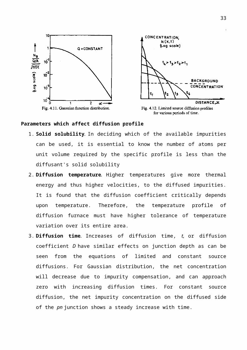
Parameters which affect diffusion profile
1. Solid solubility. In deciding which of the available impurities can be used, it is essential to
know the number of atoms per unit volume required by the specific profile is less than the
diffusant's solid solubility
2. Diffusion temperature. Higher temperatures give more thermal energy and thus higher
velocities, to the diffused impurities. It is found that the diffusion coefficient critically depends
upon temperature. Therefore, the temperature profile of diffusion furnace must have higher
tolerance of temperature variation over its entire area.
3. Diffusion time. Increases of diffusion time, t, or diffusion coefficient D have similar effects
21

on junction depth as can be seen from the equations of limited and constant source diffusions.
For Gaussian distribution, the net concentration will decrease due to impurity compensation,
and can approach zero with increasing diffusion times. For constant source diffusion, the net
impurity concentration on the diffused side of the pn junction shows a steady increase with
time.
4. Surface cleanliness and defects in silicon crystal. The silicon surface must be prevented
against contaminants during diffusion which may interfere seriously with the uniformity of the
diffusion profile. The crystal defects such as dislocation or stacking faults may produce localized
impurity concentration. This results in the degradation of junction characteristics. Hence silicon
crystal must be highly perfect.
Basic Properties of the Diffusion Process. Following properties could be considered for designing
and laying out ICs.
1. When calculating the total effective diffusion time for given impurity profile, one must
consider the effects of subsequent diffusion cycles. The effects of the subsequent diffusions on a
given impurity profile can be estimated by defining an effective (Dt) product for the particular
impurity profile as
(Dt)eff = D1t1+D2t2+ D3t3+ ... ...(10)
where t1, t2, t3 etc. are the different diffusion times and D1,D2, D3 etc. are the corresponding diffusion
coefficients as determined by the respective temperatures of the diffusion cycles.
2. The erfc and Gaussian functions show that the diffusion profiles are functions of (x/ √Dt).
Hence, for a given surface and background concentration, the junction depth x1, and x2 associated
with the two separate diffusions having different times and temperature, can be expressed as
x1 / x2 = √ D1t1 / √D2t2 ...(11)
3. Lateral Diffusion Effects. The diffusions proceed sideways from a diffusion window as well
as downward. In both types of distribution function, the side diffusion is about 75 to 80 per cent
of the vertical diffusion.
Dopants and their Characteristics
The dopant selection affects IC characteristics. Boron and phosphorus are the basic dopants of most
ICs. Arsenic and antimony, which are highly soluble in silicon and diffuse slowly, are used before
epitaxial processing or as a second diffusion. Gold and silver diffuse rapidly. They act as
recombination centres and thus reduce carrier life time. Boron is almost an exclusive choice as an
acceptor impurity in silicon since other p-type impurities have limitations as follows :
22

Gallium has relatively large diffusion coefficient in SiO2, and the usual oxide window-
opening technique for locating diffusion would be inoperative.
Indium is of little interest because of its high acceptor level of 0.16 eV, compared with 0.01
eV for boron, which indicates that not all such acceptors would be ionized at room
temperature to produce a hole. Aluminium reacts strongly with any oxygen that is present in
the silicon lattice.
The choice of a particular n-type dopant is not so limited as for p-type materials. The n-type impurities,
such as phosphorus, antimony and arsenic, can be used at different stages of IC processing. The
diffusion constant of phosphorus is much greater than for Sb and As, being comparable to that for
boron, which leads to economies resulting from shorter diffusion times.
Dopants in VLSI Technology. The common dopants in VLSI circuit fabrication are boron,
phosphorus, and arsenic. Phosphorus is useful not only as an emitter and base dopant, but also far
gettering fast-diffusing metallic contaminants, such as Cu and Au, which cause junction leakage
current problems. Thus, phosphorus is indispensable in VLSI technology. However, npn transistors
made with arsenic-diffused emitters have better low-current gain characteristics and better control of
narrow base widths than those made with phosphorus diffused emitters. Therefore, in VLSI, the use
of phosphorus as an active dopant in small, shallow junctions and low-temperature processing will be
limited to its use as the base dopant of pnp device and as a gettering agent. Arsenic is the most
frequently used dopant for the source and drain regions in n-channel MOSFETs. In the following
section, now, we will discuss some typical diffusion system. The dopant source material may be
solid, liquid or gaseous.
DIFFUSION SYSTEMS
Impurities are diffused from their compound sources as mentioned above. The method of impurity
delivery to wafer is determined by the nature of impurity source. Two-step diffusion is widely used
technique. Using this technique, the impurity concentration and profiles can be carefully controlled.
The type of impurity distribution (erfc or Gaussian) is determined by the choice of operating
conditions. The two-step diffusion consists of a deposition step and drive-in step. In the former step, a
constant source diffusion is carried out for a short time, usually at a relatively low temperatures, say,
1000°C. In the later step, the impurity supply is shutoff and the existing dopant is allowed to diffuse
into the body of the semiconductor, which is now held at a different temperature, say 1200°C, in an
oxidizing atmosphere. The oxide layer, which forms on the surface of the wafer during this step,
prevents further impurities from entering, or those already deposited, from diffusing out. The final
impurity profile is a function of diffusion conditions, such as temperature, time, and diffusion
23

coefficients, for each step.
Diffusion Furnace
For the various types of diffusion (and also oxidation) processes a resistance-heated tube furnace is
usually used. A tube furnace has a long (about 2 to 3 m) hollow opening into which a quartz tube
about 100,150 mm in diameter is placed as shown in Fig.14. The temperature of the furnace is kept
about 1000°C. The temperature within the quartz furnace tube can be controlled very accurately such
that a temperature within 1/2°C of the set-point temperature can be maintained uniformly over a "hot
zone" about 1m in length. This is achieved by three individually controlled adjacent resistance
elements. The silicon wafers to be processed are stacked up vertically into slots in a quartz carrier or
"boat" and inserted into the furnace tube.
Diffusion of p-Type Impurity
Boron is an almost exclusive choice as an acceptor impurity in silicon. It has a moderate diffusion
coefficient, typically of order 10-16m2/sec at 1150°C which is convenient for precisely controlled
diffusion. It has a solid solubility limit of around 5 x 1026 atoms/m3, so that surface concentration can
be widely varied, but most reproducible results are obtained when the concentration is approximately
1024/m3, which is typical for transistor base diffusions.
Boron Diffusion using B2H6 (Diborane) Source. This is a gaseous source for boron. This can he
directly introduced into the diffusion furnace. A number of other gases are metered into the furnace.
The principal gas flow in the furnace will be nitrogen (N2) which acts as a relatively inert gas and is
used as a carrier gas to be a dilutent for the other more reactive gases. The N2, carrier gas will generally
make up some 90 to 99 percent of the total gas flow. A small amount of oxygen and very small amount
24

of a source of boron will make up the rest of the gas flow. This is shown in Fig.15(a). The following
reactions will be occurring simultaneously at the surface of the silicon wafers :
S i+0 2 Si0 2, (silica glass)
2B2H6+ 302 B2O3 (boron glass) +6H2
This process is the chemical vapour deposition (CVD) of a glassy layer on the silicon surface which is a
mixture of silica glass (SiO2) and boron glass (B203) is called borosilica glass (BSG). The BSG glassy
layer, shown in Fig. 16, is a viscous liquid at the diffusion temperatures and the boron atoms can move
around relatively easily. Furthermore, the boron concentration in the BSG is such that the silicon
surface will be saturated with boron at the solid solubility limit throughout the time of the diffusion
process as long as BSG remains present. This is a constant source (erfc) diffusion. It is often called a
deposition diffusion. This diffusion step is referred as predeposition step in which the dopant atoms
deposit into the surface regions (say 0.3 μm depth) of the silicon wafers. The BSG is preferable
because it protects the silicon atoms from pitting or evaporating and acts as a "getter" for undesirable
impurities in the silicon. It is etched off before next diffusion as discussed below.
The predeposition step, is followed by a second diffusion process in which the external dopant source
(BSG) is removed such that no additional dopants enter the silicon. During this diffusion process the
dopants that are already in the silicon move further in and are thus redistributed. The junction depth
increases, and at the same time the surface concentration decreases. This type of diffusion is called
drive-in, or redistribution, or limited-source (Gaussian diffusion). The impurity profile for such type of
diffusion is already discussed.
The two-step diffusion combination of deposition diffusion (predeposition step) followed by a drive-in
diffusion is often used to produce the base region of transistors.
Boron Diffusion using BBr3 (Boron Tribromide) Source. This is a liquid source of boron. In this
case a controlled flow of carrier gas (N2) is bubbled through boron tribromido, as shown in Fig. 15 (b),
which with oxygen again produces boron trioxide (BSG) at the surface of the wafers as per following
reaction : 4BBr3+302 B2O 3+2Br2 Thereafter the reaction is as discussed above.
Diffusion of n-Type Impurity
For phosphorus diffusion such compounds as PH3 (phosphine) and POCl3 (phosphorus oxychloride)
can be used. In the case of a diffusion using POC13 the reactions occurring at the silicon wafer
surfaces will be: S i+0 2 SiO2 (silica glass)
4 POCl3 + 3 0 2 2P205 + 6Cl2(Phosphorus glass)
This will result in the production of a glassy layer on the silicon wafers that is a mixture of phosphorus
25

glass and silica glass called phosphorosilicaglass (PSG), which is a viscous liquid at the diffusion
temperatures. The mobility of the phosphorus atoms in this glassy layer and the phosphorus
concentration is such that the phosphorus concentration at the silicon surface will be maintained at the
solid solubility limit throughout the time of the diffusion process (similar processes occur with other
dopants, such as the case of arsenic, in which arsenosilica glass is formed on the silicon surface).The
rest of the process for phosphorus diffusion is similar to boron diffusion, i.e., after predeposition step,
drive-in diffusion is carried out. P205 is a solid source for phosphorus impurity and can be used in
place of POCl3. However, POCl3 offers certain advantages over P2O5. Such as, easier source
handling, simple furnace requirements, similar glassware for low and high surface
concentrations and better control of impurity density from wafer to wafer and from run to run.
The phosphine as a gaseous source for phosphorus can be used. But it is toxic and explosive, thus,
needs some care in handling.
Other common n-type dopants are antimony and arsenic. These dopants have low diffusion constants.
Therefore, they are useful materials for the earlier diffusion stages such as for n+ buried layers, since
once introduced they do not migrate during subsequent diffusion processes. Antimony is sometimes
preferred because it is less toxic but arsenic has a higher solid solubility limit and can provide bigger
surface concentrations of dopants.
Interstitial Dopants. Gold diffuses into silicon as an interstitial dopant. As we know, gold diffuses
very rapidly, it is often the last wafer processing step and takes place at a relatively reduced
temperature. Gold diffusion is required in silicon circuits which should operate at high speed. Gold
atoms enhance the recombination rate and so increase the switching speed. Because of the difficulty
in controlling the gold impurity profile, it is usual to coat the back of the entire wafer, using vacuum
evaporation technique, and to diffuse the impurity throughout the whole wafer to a uniform level.
Characterization of Diffused Layers
The diffused layers are characterized by two principal parameters : sheet resistance,R s, and junction
depth. Rs is expressed in ohms per square. The sheet resistance of thin layers including diffused
layers, can be conveniently measured using a four-point probe apparatus, as shown in Fig. 17. A
fixed, measured current, typically 1 mA is passed between the two outer probes and the voltage, V1,
is measured, using a high-input impedance voltmeter between the two inner probes. Current flow is
restricted to the conductivity type of the substrate. If the conditions are satisfied that the layer
thickness T is small compared to the probe spacing such that T << S, and that the edge of the layer be
relatively remote from the probe array, the sheet resistance will given approximately by Rs =(π /
log2)V/I = 4.5324. V/I
26

As a result of having separate pairs of probes for supplying the current and measuring the voltage drop,
the probe contact resistance will not influence the measurement of sheet resistance. The four point
probe can be used to measure the sheet resistance of various types of diffused layers, epitaxial layers
and that of silicon wafers for the measurement of the resistivity. The sheet resistance values of
diffused layers generally fall in the range from 1ohm/square upto about 1000 ohm/square. The
transistor base diffused layer has a sheet resistance of 200 ohm/square, and the n+ emitter diffused
layer has down the range of around 2 ohm/square.
27

ION IMPLANTATION
Ion implantation is an alternative to deposition diffusion and is used to produce a shallow surface
region of dopant atoms deposited into a silicon wafer. In this process a beam of impurity ions is
accelerated to kinetic energies in the range of several tens of kV and is directed to the surface of the
silicon. As the impurity atoms enter the crystal, they give up their energy to the lattice in collisions
and finally come to rest at some average penetration depth, called the projected range expressed in
μm. Depending on the impurity and its implantation energy, the range in a given semiconductor may
vary from a few hundred angstroms to about 1 μm. Typical distribution of impurity about the
projected range is approximately Gaussian. By performing several implantations at different energies,
it is possible to synthesize a desired impurity distribution, uniformly doped region.
Ion Implantation System
A typical ion implantation system is shown in Fig. 18.
A gas containing the desired impurity is ionized within the ion source. The ions are generated and
repelled from their source in a diverging beam that is focused before it passes through a mass
28

separator that directs only the ions of the desired speed through a narrow aperture. A second lens
focuses this resolved beam which then passes through an accelerator that brings the ions to their
required energy before they strike the target and become implanted in the exposed areas of the silicon
wafers. The accelerating voltages may be from 20 kV to as much as 250 kV. In some ion implanters,
the mass separation occurs after the ions are accelerated to high energy. Because the ion beam is small,
means are provided for scanning it uniformly across the wafers. For this purpose the focused ion beam
is scanned electro statically over the surface of the wafer in the target chamber. Repetitive scanning in
a raster pattern provides exception uniform doping of the wafer surface. The target chamber commonly
includes automatic wafer handling facilities to speed up the process of implanting many wafers per
hour.
Annealing after Implantation.
After the ions have been implanted they are lodged principally in interstitial positions in the silicon
crystal structure, and the surface region into which the implantation has taken place will be heavily
damaged by the impact of the high energy ions. The disarray of silicon atoms in the surface region is
often to the extent that this region is no longer crystalline in structure but, rather, amorphous. To
restore this surface region back to a well ordered crystalline state and to allow the implanted ions to go
into substitutional sites in the crystal structure, the wafer must be subjected to an annealing process.
The annealing process usually involves the heating of the wafers to some elevated temperature, often
in the range of 1000°C for a suitable length of time such as 30 minutes. Laser beam and electron
beam annealing are also employed. In such annealing techniques only the surface region of the wafer
is heated and recrystallized. An ion implantation process is often followed by a conventional type
drive-in diffusion, in which case the annealing process will occur as part of the drive-in diffusion. Ion
implantation is a substantially more expensive process than conventional deposition diffusion, both in
terms of the cost of the equipment and the throughput.
High-Current High-Energy Implantation Machines
The ion-implantation apparatus, discussed above, has limits to energy range. The minimum
implantation energy is usually set by the extraction voltage, i.e., the voltage causing the ions to move
out of the ion source into the mass separator. This voltage (which is typically 20 KeV) cannot be
reduced too far without drastically reducing beam current. The maximum implantation energy is set by
the design of the high voltage equipment. The only way to circumvent this is to implant multiply
charged ions. For example, instead of implanting B+(boron ion), we can implant B++ . The B++ion would
receive twice the energy of B+ from the same accelerating potential, effectively doubling the energy of
29

the machines. The price paid is a reduced beam current since the number of B++ ions in the source
plasma is much smaller.
It is advantageous to increase beam current since it improves implanter throughput by reducing the
time for each implantation step. High-current machines can deliver at least 5 mA ion-beam currents, so
that 150 mm wafers can be given a dose of 1015 ions/cm2 in only 6 seconds per wafer [A medium-
energy ion implanter consuming 45 kW of power can process 200 wafers (100 mm diameter) with a
dose of 1015 ions/cm2 ]High beam currents are obtained by using multiple extraction electrodes and
higher voltages. To get a final beam of suitable energy a combination of acceleration and deceleration
modes of operation is used. The electrostatic scanning is not suitable for high beam currents as it
disrupts space charge neutrality and leads to beam "blow-up". Therefore a mechanical scanning system
is usually used. In this case, the wafer is scanned past a stationary beam. This method has the added
advantage of keeping the same beam angle across the whole wafer, whereas an electrostatic system can
vary by ± 2° for 100 mm wafers. However, mechanical scanning puts new requirements on the wafer
holder.
High energy implantation, at MeV energies, makes possible several new processing techniques
required for VLSI. For example, buried conductors are very useful in VLSI CMOS circuits. In such
circuit fabrication high substrate doping is needed to lower voltage drop from substrate currents and so
prevent latch up, and at the same time low substrate doping is needed to minimize junction
capacitance. High energy ion implantation offers better solution for such fabrication problem.
Buried insulator is another example where high-energy implantation is required. Buried insulators are
employed in VLSI fabrication, since they offer a compact way to isolate devices from each other and
to reduce parasitic capacitance. The high-energy implantation permits formation of buried insulators
by implantation of oxygen or nitrogen as an alternative to the epitaxial growth of silicon on sapphire
(SOS).
Properties of Ion Implantation
The depth of penetration of any particular type of ion will increase with increasing accelerating
voltage. The penetration depth will generally be in the range of .1 to 1.0 μm. Table below shows
various projected ranges, Rp, for various typical accelerating voltages for boron and phosphorus ions
in silicon.
Table 1. Projected Ranges(Rp)for Boron and (Rn) for Phosphorus Ions in Silicon
Energy (k V) Rp of boron (μm) R n o f p h o s p h o r o u s (μm)
30

20 0.067 0.026
100 0.30 0.123
200 0.52 0.254
300 0.70 0.386
Impurity Distribution of Implanted Ions.
Fig 19 Ion Implantation profile
The distribution of the implanted ions as a function of distance ,x from the silicon surface will be a
Gaussian distribution, given by
N (x) = Np exp ( - (x- Rp) 2 /2∆ Rp2)
where x = distance into substrate from surface
Rp = projected range
∆ Rp = straggle (standard deviation) of the projected range
Np = peak concentration of implanted ions.
An ion implantation impurity profile is shown in Fig.19. The peak implanted ion concentration is
related to the implantat ion dosage Q by Np= Q/ √2π∆ Rp…………………..(14)
The implantation dosage Q is the number of implanted ions per unit of surface area as given by such
units as ions/cm2. The ion density drops off rapidly from the peak value with distance as measured
from Rp in either direction. Note that the Gaussian implanted ion profile will be truncated at x = 0
Advantages of Ion Implantation.
(i) Ion implantation provides much more precise control over the density of dopants (Q)
deposited into the wafer, and hence the sheet resistance. This is possible because
both the accelerating voltage and the ion beam current are electrically controlled
outside of the apparatus in which the implants occur.
(ii) Very low dosage, low energy implantations are also used for the adjustment of the
31

threshold voltage of MOSFETs and other applications.
(iii) It can be done at relatively low temperatures, this means that doped layers can be
implanted without disturbing previously diffused regions. This means a lesser
tendency for lateral spreading.
(iv) A precise quantity of impurity can be introduced. Since the beam current can be
measured accurately during implantation
This control over doping level, along with the uniformity of the implant over the wafer surface, make
ion implantation attractive for the IC fabrication, since this causes significant improvement in the
quality of an IC. Due to precise control over doping concentration, it is possible to have very low
values of dosage Q (< 1014cm-3), so that very large values of Sheet resistance (>1000ohm/square) can
be obtained. These high sheet resistance values are useful for obtaining large value resistors (≥50KΩ)
for ICs.
Importance of Ion Implantation for VLSI Technology.
Ion implantation is a very popular process for VLSI because it provides more precise control of
dopants (as compared to diffusion) from 1011 atoms/ cm2 to greater than 1016 atoms/cm2. With the
reduction of device sizes to the submicron range, the electrical activation of ion-implanted species
relies on a rapid thermal annealing technique, resulting in as little movement of impurity atoms as
possible. Thus, diffusion process has become less important than methods for introducing impurity
atoms into silicon for forming very shallow junctions, an important feature of VLSI circuits. Ion
implantation permits introduction of the dopant in silicon that is controllable, reproducible, and free
from undesirable side effects. Its attributes of controllability and reproducibility make it a very
versatile tool, able to follow the trends to finer-scale devices.
THERMAL OXIDATION
Oxidation is the process of growing Silicon dioxide layer of 0.02 to 2 μm thickness over the surface
of Si wafer by exposing the wafer to an Oxygen atmosphere at about 1000°C to prevent the N type
epitaxial layer from getting contaminated by the surrounding atmosphere. Oxidation furnace is used
for this purpose. Thickness of oxide layer depends on temperature of the furnace, the length of time
that wafers are in it and flow rate of oxygen. The rate of oxidation can be significantly increased by
adding water vapour to the oxygen supply to the oxidizing furnace.
Utility of Thermal Oxidation
The function of a layer of silicon dioxide (SiO2) on a chip is multipurpose. SiO2 plays an important
role in IC technology because no other semiconductor material has a native oxide which is able to
32
achieve all the properties of SiO2. The role of SiO2 in IC fabrication is as below :
1. It acts as a diffusion mask permitting selective diffusions into silicon wafer through the
window etched into oxide.
2. It is used for surface passivation which is nothing but creating protective SiO2 layer on the
wafer surface. It protects the junction from moisture and other atmospheric contaminants.
3. It serves as an insulator on the water surface. Its high relative dielectric constant, 3.9, which
enables metal line to pass over the active silicon regions.
4. SiO2 acts as the active gate electrode, in MOS device structure.
5. It is used to isolate one device from another (dielectric isolation as opposed to junction
isolation).
6. It provides electrical isolation of multilevel metallization used in VLSI.
Growth and Properties of Oxide Layers on Silicon
Silicon dioxide (silica) layer is formed on the surface of a silicon wafer by thermal oxidation at high
temperatures in a stream of oxygen in an oxidation furnace similar to diffusion furnace.
Si + 02 SiO2 (solid)
Si +2H2O S i O 2 +2H2
The time and temperature required to produce a particular layer thickness are obtained from
empirically determined design curves, of the type shown in Fig. 20 corresponding to dry oxygen
atmosphere and Fig. 21 corresponding to steam atmosphere. Layer thickness in the range 0.1 to 5
33
μm are commonly produced at a temperatures between 1000 and 1200 °C. A typical schedule might
be to bubble oxygen through water into a furnace at 1100°C, to give an oxide growth rate of around
0.5 μm per hour. The minimum thickness of oxide required for the complete masking of a particular
dopant depends on the dopant and the diffusion parameters, e.g., time and temperature.
Growth Rate of Silicon Oxide Layer
The initial growth of the oxide is limited by the rate at which the chemical reaction takes place.
After the first 100 to 300Å of oxide has been produced, the growth rate of the oxide layer will be
limited principally by the rate of diffusion of the oxidant ( 0 2 or H20) through the oxide layer, as
shown in Fig. 22(a).The rate of diffusion of 02 or H2O through the oxide layer will be inversely
proportional to the thickness of the layer, so that we will have that
dx /dt = C/ x
where x is the oxide thickness and C is a constant of proportionality. Rearranging and integrating
this both sides yields x2/2 =Ct or x =√2Ct. We see that after an initial reaction-rate limited
linear growth phase (tox α time), the oxide growth will become diffusion-rate limited with the oxide
thickness increasing as the square root of the growth time. Fig. 22 (b). The rate of oxide growth
using H2O as the oxidant will be about four times faster than the rate obtained with 02. This is due to
the fact that the H2O molecule is about one-half the size of the O2, molecule, so that the rate of
diffusion of H2O through the SiO2layer will be much greater than the 02 diffusion rate.
Although the oxide growth rate with H2O is much faster than with 02, the "dry" (02) oxide will be a
slightly denser oxide with a higher dielectric strength than the "wet" (H20) oxide. In many cases a "dry-
wet-dry" oxidation process is used, starting off the initial oxide growth using 02. This is followed by a
H2O oxide growth phase to produce the bulk of the oxide thickness, and then completed by a final
34

"dry" oxidation. This will produce a composite oxide layer as shown in Fig. 23 with the denser "dry"
oxide regions being adjacent to the silicon surface and serving as a protective cap on top, and the less
dense "wet" oxide being sandwiched in between. It should be noted that in the themal growth process of
an oxide layer some silicon from the substrate is consumed. If the resulting thickness of the SiO2layer is
designated as tox, the thickness of the silicon consumed will be 0.44 tox
Oxide Charges
The interface between silicon and silicon dioxide contains a transition region. Various charges are
associated with the oxidized silicon, some of which are related to the transition region. A charge at the
interface can induce a charge of the opposite polarity in the underlying silicon, thereby affecting the
ideal characteristics of the MOS device. This results in both yield and reliability problems. Fig. 24 shows
general types of charges.
Interface-trapped charges. These charges at Si-SiO2 are thought to result from several sources,
including structural defects related to the oxidation process, metallic impurities, or bond breaking
processes. The density of these charges is usually expressed in terms of unit area and energy in the
silicon bandgap (number/cm2-eV). Values of 1010/cm2-eV and lower have been observed.
Fixed oxide charge. This charge (usually positive) is located in the oxide within approximately 30 Å
of the Si-SiO2 interface. Fixed oxide charge cannot be charged or discharged. Its density ranges from
1010/cm2 to 1012/cm2. Its values for<100> oriented silicon are less than those for <111> silicon. This
difference is related to the number of available bonds per unit area of silicon surface. From a
processing point of view, fixed oxide charge is determined by both temperature and ambient
conditions.
Mobile ionic charge. This is attributed to alkali ions such as sodium, potassium, and lithium in the
oxides as well as to negative ions and heavy metals. The alkali ions are mobile even at mom
temperature, when electric fields are present. Densities range from 1010/cm2to 1012/cm2 or higher and
are related to processing materials, chemicals, ambient, or handling.
Oxide trapped charge. This charge may be positive or negative, due to holes or electrons trapped in
the bulk of the oxide. This charge, associated with defects in the SiO2, may result from ionizing
radiation, avalanche injection, or high currents in the oxide. Densities range from less than 109/cm2 to
1013/cm2.
The effects of various charges can be minimized as follows. The interfaced-trapped charge can be
neutralized by a low temperature hydrogen annealing (450°C). Fixed oxide charge is minimized by
35

inert ambient annealing. The mobile ionic charge can be minimized by cleaning the furnace tube in a
chlorine ambient, gettering with phosphosilicate glass, and using masking layers such as silicon
nitride. The oxide-trapped charge can be annealed out by low-temperature treatment.
Effect of Impurities on the Oxidation Rate
The following impurities affect the oxidation rate (i) water (ii) sodium (iii) group III and V elements,
and (iv) halogen. In addition damage to the silicon also affects oxidation rate.
As we discussed that wet oxidation occurs at a substantially greater rate then dry oxygen, any
unintentional moisture accelerates the dry oxidation. High concentrations of sodium influence the
oxidation rate by changing the bond structure in the oxide, thereby enhancing the diffusion and
concentration of the oxygen molecules in the oxide. During thermal oxidation process, an interface is
formed, which separates the silicon from silicon dioxide. As oxidation proceeds, this interface
advances into the silicon. A doping impurity, which is initially present in the silicon, will redistribute at
the interface until its chemical potential is the same on each side of the interface. This redistribution
may result in an abrupt change in impurity concentration across the interface. The ratio of the
equilibrium concentration of the impurity, i.e., dopant in silicon to that in SiO2 at the interface is called
the equilibrium segregation coefficient. The redistribution of the dopants (group III or V elements) at
the interface influences the oxidation behaviour. If the dopant segregates into the oxide and remains
there (such as Boron, in an oxidizing ambient), the bond structure in the silica weakens. This weakened
structure permits an increased incorporation and diffusivity of the oxidizing species through the oxide,
36

thus enhancing the oxidation rate. Impurities that segregate into the oxide but then diffuse rapidly through
it (such as aluminium, gallium, and indium) have no effect on the oxidation kinetics. Phosphorus
impurity shows opposite effect to that of boron, i.e., impurity segregation occurs in silicon rather than
SiO2. The same is true for As and Sb dopants.
Halogen (such as chlorine) impurities are intentionally introduced into the oxidation ambient to improve
both the oxide and the underlying silicon properties. Oxide improvement occurs because there is a
reduction in sodium ion contamination, increase in oxide breakdown strength, and a reduction in
interface trap density. Traps are energy levels in the forbidden energy gap which are associated with
defects in the silicon.
Thermal Oxidation Practice
The oxidation practice employed depends upon the thickness and oxide properties required. For oxide
thickness more than 0.5 μm, steam is used (~1 atm or an elevated pressure). Higher pressure allows
thick oxide growth to be achieved at moderate temperatures in reasonable amounts of time. One
atmosphere oxide growth, the most commonly used technique, is typically carried out in a horizontal
diffusion tube, although vertical diffusion furnaces are being used more frequently. In the case of the
horizontal furnace, the wafers are held vertically in a slotted paddle (boat), which is normally loaded
using cassette-to-cassette equipment. Typical oxidation temperatures range from 700 to 1200°C
and could be held to within ±1°C to ensure uniformity. In a standard procedure the wafers are
chemically cleaned, dried, loaded onto the paddle, and automatically inserted into the 700 to 900°C
furnace, which is then ramped up to oxidation temperature. Ramping is used to prevent wafer warpage.
Following oxidation, the furnace is ramped down and the wafers are removed. Eliminating particles
during oxidation is necessary to grow high-quality, reproducible oxides. Innovative designs now use a
cantilevered arrangement in which the paddle is inserted into the oxidation tube in a contactless
manner and then lowered onto the tube.
Before thermal oxidation process, the wafers must be cleaned to eliminate both organic and inorganic
contamination arising from previous processing steps and handling such contaminations, if not
removed, can degrade the electrical characteristics of the devices and can contribute to reliability
problems. A common cleaning procedure uses a H20—H202—NH4OH mixture to remove organic
contamination by the solvating action of the ammonium hydroxide and the oxidizing effect of the
peroxide. To remove heavy metals a H2O—H2O2–HCl solution is commonly used. Modern diffusion
(oxidation) furnaces are microprocessor controlled to provide repeatable sequencing, temperature
control, and gas flow control. The entire procedure, from boat loading to boat withdrawal, is
37

programmed.
High Pressure Oxidation
The rate of diffusion of the oxidant molecules through an oxide layer is proportional to the ambient
pressure. For example, at a pressure of 10 atm the diffusion rate will be increased by a factor of 10
and the corresponding oxidation time can be reduced by nearly the same factor. Alternatively, the
oxidation can be done for the same length of time, but the temperature required will be substantially
lower. For example, a steam (H20) oxidation at 1200°C and a 1.0 atm ambient pressure will produce
an oxide layer that is 0.6 μm thick, for an oxidation time of 36 minutes. The same thickness of oxide
can be produced in the same period of time at a temperature of only 920°C, if the ambient pressure is
increased to 10 atm. As a second example, a 10 hour steam oxidation at 920°C and at 1.0 atm ambient
pressure will result in 0.2 μm -thick oxide. If the ambient pressure is increased to 10 atm, the
temperature can be reduced to only 795°C for the same oxide thickness produced in the same period
of time. Principal benefit of high-pressure oxidation processing is lower-temperature processing. The
lower processing temperature reduces the formation of crystalline defects and produces less
effect on previous diffusions and other processes. The shorter oxidation time is also
advantageous in increasing the system throughput. The major limitation of this process is the
high initial cost of the system.
The anodic plasma-oxidation which offers the possibility of growing high quality oxides at
temperatures even lower than those achieved with the high pressure technique. This process has all
the advantages associated with low temperature processing. Anodic plasma oxidation can grow
reasonably thick oxides of the order of 1 μm at low temperatures (<600°C) at growth rates upto about
1 μm/hr. Plasma oxidation is a low-temperature vacuum process, usually carried out in a pure oxygen
discharge.
Oxide Masking and Oxide Passivation
Oxide Masking. Oxide layer is used to mask an underlying silicon surface against a diffusion (or ion
implantation) process. The oxide layer is patterned by the photltithographic process to produce regions
where there are opening or "windows" where the oxide has been removed to expose the underlying
silicon. Then these exposed silicon regions are subjected to the diffusion (or implantation) of dopants,
whereas the unexposed silicon regions will be protected. The pattern of dopant that will be deposited
into the silicon will thus be a replication of the pattern of opening in the oxide layer. The replication
is a key factor in the production of tiny electronic components. The thickness of oxide needed for
diffusion masking is a function of the type of diffusant and the diffusion time and temperature
conditions. In particular, an oxide thickness of some 5000 Å will be sufficient to mask against almost
38

all diffusions. This oxide thickness will also be sufficient to block almost all but the highest energy
ion implantation.
Oxide Passivation. The surface passivation is nothing but creating protective SiO2 layer on the wafer
surface. Fig. 25 shows a cross-sectional view of a pn junction produced by diffusion through an oxide
window. The junction depth in the vertical direction is indicated as x j. The distance from the edge of
the oxide window to the junction in the lateral direction underneath the oxide is indicated as yj. The
relationship between yj and xj is that yj = 0.8 xj so that the curvature of the junction in the regions
underneath the edge of the oxide window is nearly that of a quarter circle with a radius of curvature
that is nearly equal to the junction depth. In Fig. 25 we note that the junction intersects the silicon
surface well underneath the protective thermally grown oxide layer. This oxide layer protects the
junction against various environmental effects, and is therefore called a passivated junction. We also
note that the locus of intersection of the junction depth with the silicon surface is entirely within a
single geometric plane, and for that reason this type of junction is called a planer junction. Note that
the junction itself is not flat or plane, but rather there is a curvature of the junction in the region
underneath the edges of the oxide window. This junction curvature will result in an increase in the
electric field intensity in these regions which will cause the break down voltage of the junction to be
lower than that of a corresponding plane junction with the same doping levels.
LITHOGRAPHY
The lithography technique was first used in the late eighteenth century by people interested in art. A
lithograph is a less expensive picture made from a flat, specially prepared stone or metal plate and the
lithography is art of making lithographs. Therefore, lithography for IC manufacturing is analogous to
39

the lithography of the art world. The selective removal of the oxide in the desired area is performed by
lithographic process. In this process the exposing radiation, such as ultraviolet (UV) light in case of
photolithography, is transmitted through the "clear" parts of the mask. The circuit pattern of opaque
chromium blocks some of the radiation. This type of chromium/glass mask is used with UV light. Other
types of exposing radiations are electrons, X-rays, or ions. Thus, for IC manufacturing we have
following types of lithography :
Lithography can be divided into
1. Photo Lithography.
2. Fine Line Lithography. This is further classified as
i. Electron-beam lithography
ii. X-ray lithography
iii. Ion-beam lithography
In IC fabrication number of masks are employed. Except for the first mask, every mask must be aligned
to the pattern produced by the previous mask. This is done using mask aligner. The mask aligner
may be contact type or proximity type or projection type. Accordingly we have three types of
printing :
(i) Contact printing, (ii) Proximity printing and (iii) Projection printing.
Photolithographic Process
Photolithography or optical lithography is a kind of lithography used for selective removal of the oxide
in the desired area. Thus, the areas over which diffusions are effective are defined by the oxide layer
(which inhibits diffusion) with windows cut in it, through which diffusion can take place. The
windows are produced by the photolithographic process. This process is the means by which
microscopically small circuit and devices can be produced on silicon wafers, resulting in as many as
10000 transistors on a 1 cm x 1 cm chip.
Steps involved in Photolithographic Process are as follows
(i) Photoresist Application (Spinning). A drop of light sensitive liquid called photoresist is applied
to the centre of the oxidized silicon wafer that is held down by a vacuum chuck. The wafer is then
accelerated rapidly to a rotational velocity in the range 3000 to 7000 RPM for some 30 to 60 seconds.
This action spreads the solution in a thin, nearly uniform coat and spins off the excess liquid. The
thickness of the coat so obtained is in the range 5000 to 10000 Å, as shown in Fig. 26(a). The
thickness of the photoresist layer will be approximately inversely proportional to the square root of
40

the rotational velocity. Sometimes prior to the application of the photoresist the silicon wafers are
given a "bake-out" at a temperature of at least 100°C to drive off moisture from the wafer surfaces so as
to obtain better adhesion of the photoresist. Typical photoresist used is Kodak Thin Film Resist
(KTFR).
(ii) Prebake. The silicon wafers coated with photoresist are now put into an oven at about 80°C for
about 30 to 60 min. to drive off solvents in the photoresist and to harden it into a semisolid film.
(iii) Alignment and Exposure. The coated wafer, as above, is now placed in an apparatus called a
mask aligner in very close proximity (about 25 to 125 μm) to a photo mask. The relative positions of
the wafer and the photomasks are adjusted such that the photomask is correctly lined up with reference
marks or a pre-existing pattern on the wafer. The photomask is a glass plate, typically about 125 mm
square and about 2 mm thick. The photomask has a photographic emulsion or thin film metal
(generally chromium) pattern on one side. The pattern has clear and opaque areas. The alignment of
the photomask to the wafer is often required to be accurate to within less than 1 μm, and in some cases
to within 0.5 μm. After proper alignment has been achieved, the wafer is brought into direct contact
with the photomask. A highly collimated ultraviolet (UV) light is then turned on and the areas of the
silicon wafer that are not covered by the opaque areas of the photomask are exposed to ultraviolet
radiation, as shown in Fig.26 (b). The exposure time is generally in the range 3 to 10sec. and is
carefully controlled such that the total UV radiation dosage in watt-seconds or joules is of the
required amount
(iv) Development. In the present description negative photoresist is used in which the areas of the
photoresist that are exposed to the ultraviolet radiation become polymerized. The polymerization
process increases the length of the organic chain molecules that make up the photoresist. This makes
the resist tougher and makes it essentially insoluble in the developer solution. The resisting
photoresist pattern after the development process will therefore be a replication of the photomask
pattern, with the clear areas on the photomask corresponding to the areas where the photoresist
remains on the wafers, as shown in Fig.26(c). An opposite type of process occurs with positive
photoresist. Exposure to UV radiation results in deploymerization of the photoresist. This makes
these exposed areas of the photoresist readily soluble in the developer solution, whereas the
unexposed areas are essentially insoluble. The developer solution will thus remove the exposed or
depolymerized regions of the photoresist, whereas the unexposed areas will remain on the wafer.
Thus again there is a replication of the photomask pattern, but this time the clear areas of the
photomask produce the areas on the wafer from which the photoresist has been removed.
(v) Postbake. After development and rinsing the wafers are usually given a postbake in an oven at
41

a temperature of about 150°C for about 30 to 60 min. to toughen further the remaining resist on the
wafer. This is to make it adhere better to the wafer and to make it more resistant to the hydrofluoric
acid (HF) solution used for etching of the silicon dioxide.
(vi) Oxide Etching. The remaining resist is hardened and acts as a convenient mask through which
the oxide layer can be etched away to expose areas of semiconductor underneath. These exposed
areas are ready for impurity diffusion. For etching of oxide, the wafers are immersed in or sprayed
with a hydrofluoric (HF) acid solution. This solution is usually a diluted solution of typically 10 : 1,
H2O : HF, or more often a 10 : 1 NH4F (ammonium fluoride) : HF solution. The HF solutions will
etch the SiO2 but will not attack the underlying silicon, nor will it attack the photoresist layer to any
appreciable extent. The wafers are exposed to the etching solution long enough to remove the SiO 2
completely in the areas of the wafer that are not covered by the photoresist, as shown in Fig. 26(d).
For the 10:1 buffered HF solution (NH4F : HF) the SiO2 etching rate is about 1000 A/min. at 25°C so
that only about 5 min. will be required to remove a typical oxide layer of 5000 Å. thickness. The
result of the oxide etching process will be a pattern of openings or windows in the SiO2layerthat will
replicate the photoresist pattern, and will therefore be a replication of the pattern on the photomask.
The duration of oxide etching should be carefully controlled so that all of the oxide present only in the
photoresist window is removed. If etching time is excessively prolonged, it will result in more
undercutting underneath the photoresist and widening of the oxide opening beyond what is desired.
The above oxide etching process is termed wet etching process since the chemical reagents used are
in liquid form. A newer process for oxide etching is a dry etching process called plasma etching.
Another dry etching process is ion milling.
(vi) Photoresist Stripping. Following oxide etching, the remaining resist is finally removed or stripped
off with a mixture of sulphuric acid and hydrogen peroxide and with the help of abrasion process.
Finally a step of washing and drying completes the required window in the oxide layer. Fig. 26(e)
shows the silicon wafer ready for next diffusion. Negative photoresists, as above, are more difficult to
remove. Positive photoresists can usually be easily removed in organic solvents such as acetone.
The photolithography may employ contact, proximity, or projection printing. For IC production the
line width limit of photolithography lies near 0.4 μm, although 0.2 μm features may be printed under
carefully controlled conditions. At present, the photolithography occupies the primary position
among various lithographic techniques.
42

Photoresists
One of the major factors in providing increasingly complex devices has been improvement in
photolithographic art. A large part of this improvement has been due to high quality photoresist,
materials as improved techniques of coating, baking, exposing and developing photoresists.
The principal constituents of a photo resist solution are a polymer, a sensitizer and a suitable
solvent system. Polymers have properties of excellent film forming and coating. Polymers generally
used are polyvinyl cinnamate, partially cyclized isoprene family and other types are phenol
formaldehyde, Novolac etc. When photoresist is exposed to light, sensitizer absorbs energy and
initiates chemical changes in the resist. The sensitizers are chromophoric organic molecules. They
greatly enhance cross linking of the photoresist. Cross linking of polymer or long chain formation of
considerable number of monomers makes high molecular weight molecules on exposure to light
radiation, termed as photo-polymerization. Typical sensitizers are carbonyl compounds. Benzoin,
Benzoyl peroxide, Benzoyl disulphide, nitrogen compounds and halogen compounds. The
solvents used to keep the polymers in solution are mixture of organic liquids. They include aliphetic
esters such as butyl acetate and cellosolve acetate, aromatic hydrocarbons like xylene and
Ethylbenzene, chlorinated hydrocarbons like chlorobenzene and methylene chloride and ketones such
as cyclohexanone. The same solvents are used as thinners and developers.
Characteristics of Good Photoresist. To achieve faithful registration of the mask geometry over the
substrate surface, the resist should satisfy following conditions:
43

(i) Uniform film formation
(ii) Good adhesion to the substrate
(iii) Resolution and
(iv) Resistance to wet and dry etch processes.
Types of Photoresist. Two types of photoresist exist : negative photoresist and positive
photoresist. According to the changes that take place, photoresists are termed negative or positive.
Materials which are rendered less soluble in a developer solution by illumination, yield a negative
pattern of the mask and are called negative photoresists. Conversely, positive photoresists become
more soluble when subjected to light and therefore yield a positive image of the mask. The selection of
photoresist depends upon specific requirement resolution and type of surface to be encountered.
Differences in solid content and viscosity determine the flow characteristics and thus the thickness of
coating. The development of modern photoresist originated at Eastman Kodak Research Laboratory.
Now-a-days there are number of manufactures producing photoresists, they are : Eastman Kodak
Company, Waycoat Hunt, J.T. Bakers, VLSI Photoresists, Microimage Inc., Shipley Co. etc.
Polymers film is either photosensitive or capable or reacting with the pholysis product of additional
compound so that the solubility increases or decreases greatly by exposure to UV (ultra-violet)
radiation.
Negative Photoresist. Kodak negative photoresist contain polyvinyl cinnametes with sulfur
compounds of the nepthothizol group sensitizer. KPR is being used in printing circuit boards. KTFR
is widely used for fabrication of ICs. It provides good adhesion to silicon dioxide and metal surfaces.
It gives good etch resistance to different etchant solutions. For finer resolution, thinner coating of
KTFR is used. To achieve coating of controlled and uniform thickness, the viscosity of resist is
suitably lowered using thinners. The sensitivity of the negative photoresist to light and electrons is
increased by mixing certain chemical additives resulting in shorter exposure time. Good results are
obtained by adding 1% Benzophenone into KTFR solution. Another negative photoresist is Kodak
Micron eg 747 which is particularly suited to projection printing where it provides high scan speeds at
high aperature giving high throughput and resolution. The film forming component of this resist is a
chemically inert polyisoprene rubber. The sensitizer part of the resist on exposure to light reacts with
the rubber to form cross links between rubber molecules, making the rubber less soluble in an organic
developer solvent. The reactive species formed during the exposure can react with oxygen and be
rendered ineffective for crosslinking. Therefore the resist is usually exposed in a nitrogen atmosphere.
The solvent dissolves the unexposed resist. The exposed resist swells as the uncrosslinked molecules
are dissolved. The swelling distorts the pattern features and limits resolution to 2 to 3 times the initial
44

film thickness. In general, negativephotoresist display excellent adhesion, etch resistance and resolution
on all surfaces. However, they have following drawbacks. As resolution gets finer and finer coated
layer thickness also has to be miner and thinner. This thinning of coating introduces pin holes and
decreases etch resistance. Also, for reason mentioned above, there is limit to resolution as compared to
positive photoresist discussed below.
Positive Photoresist. Positive types of resist were introduced in 1960. This has solved the problems
of resolution and substrate protection. Positive resist can be used at a coating thickness 1 μm that
eliminates pin holes and minimizes defects from dust ant still capable of sub-micron resolution.
Positive photoresist is inherently of low solubility (polymerized) material. The base polymer is not
active by itself. A sensitizer, when absorbs light, makes the base resist soluble in an alkali developer.
Positive photoresists are Novolac resins with one of several possible Napthoquinone diazides
functioning as sensitizers. Typical solvents are cellosolve acetate, butyl acetate, xylem and toluene.
Higher resolution is provided by positive photoresist as stated above. This can be understood as follows.
Positive photoresist has two components: a resin and a sensitizer dissolved in a solvent. The
sensitizer compound is a dissolution inhibitor. When it is destroyed by exposure to light, the resin
becomes more soluble in an aqueous developer solution, as stated above. The unexposed regions do not
swell much in the developer solution, so higher resolution is possible with positive resists. The
sensitivity of most standard resists peaks in the 300 to 400 nm spectral range. Two examples of
positive resists are MP-2400 and HPR-206. Photoresists are being developed for exposure at shorter
wavelengths where higher resolution is possible. A few such deep UV resists are polymethyl
methacrylate (PMMA), sensitive for wavelength (λ.) <250 nm, polybutene sulfone, sensitive for λ ≤
200nm, and MP-2400, sensitive for λ = 200 nm.
Resist requirements for VLSI. For fine line geometries in VLSI circuits, the resist requirements
become more stringent. The resist properties should meet the required demand of higher resolution.
Hence the resist should exhibit
(i) High sensitivity for particular exposure tool chosen,
(ii) Dry developing, dry etch compatibility, and
(iii) Vertical profile control.
Resist Sensitivity. Sensitivity of a resist as defined by the required incident dose (charge per area) is
strongly influenced by many parameters including incident light energy, resist thickness, polymer
molecular weight and its distribution. Negative resists are in general-more sensitive than positive
resists. Polymethyl Methacrylate Methacrylic acid with large molecular weight shows very high
sensitivity.
45
Dry Development. Plasma development resists offer the advantage of development in an etch like
manner which avoids the resolution limitations encountered during the solution development of most
negative resists. Originally, plasma developed resists contained only organic components. Now, the
trend in dry developed resist materials is to incorporate inorganic materials as well. The IBM group
used thin poly (Siloxane) films (2000 Å) on hardened AZ 1350 J resist and exposed them to deep ultra
violet radiation (200-260 nm). The 0.5 μm isolated line was resolved by contact lithography.One of
the more difficult problems with resist pattern generation is to achieve good line width control, high
resolution and good step coverage simultaneously. Fine resolution with conventional lithography can
be achieved by improvement in optics or greatly improved resist materials and process. Combination of
both can give best chance of achieving fine resolution in optical lithography. The problem of
resolution can be eliminated by using a multilayer resist structure, i.e., bi-and-tri-layer systems.
Photomask Fabrication Steps
Photolithography is used to produce windows in the oxide layer of the silicon wafer, through which
diffusion can take place, for this purpose photomask is required. The pattern appearing on the mask is
required to be transferred to the wafer. For this purpose various exposure techniques are employed.
Mask Making. IC fabrication is done by the batch processing, where many copies of the same circuit
are fabricated on a single wafer and many wafers are fabricated at the same time. The number of
wafers processed at one time is called the lot size and many vary between 20 to 200 wafers. The
number of ICs per wafer is a function of the size of the IC (called chip size or die size) and the diameter
of the wafer. Since each IC chip is square and the wafer is circular, the number of chips per wafer is the
number of complete squares of a given size that can fit inside a circle. This number can be calculated
as follows :
Number of chips (dice) = π r2 / A — 1.77 d/√A ………………….(16)
where d = diameter of wafer, A = area of chip (die), r = radius of wafer
The pattern for the mask is designed from the circuit layout. Many years ago, "bread boarding" of the
circuit was typical. In this, the circuit was actually built and tested with discrete components before
its integration. At present, however, when LSI and VLSI circuits contain from a thousand to several
hundred thousand components, and switching speeds are of such high order where propagation delay
time between devices is significant, bread boarding is obviously not practical. Present-day mask
layout is done with the help of computer. The photographic mask determines the location of all
windows in the oxide layer, and hence areas over which a particular diffusion step is effective. Each
complete mask consists of a photographic plate on which each window (to be opened before the next
diffusion of impurity) is represented by an opaque area, the remainder being transparent. Each
46

complete mask will not only include all the windows for the production of one stage of a particular IC,
but in addition, all similar areas for all such circuits on the entire silicon wafer, as shown in Fig.
It will be obvious that a different mask is required for each stage in the production of an array of ICs
on a wafer. There is also a vital requirement for precise registration between one mask and the other
in the series, to ensure that there is no overlap between components, and that each section of a particular
transistor, say, is formed in precisely the correct location.
To make a mask for one of the production stages, a master is first prepared which is an exact replica
of that portion of the final mask associated with one individual integrated circuit, but which is 250 x
(say) enlargement of the final size of IC. Fig. above shows a possible master for the production of a
mask to define a particular layer of diffusion for a hypothetical circuit. Artwork at enlarge size avoids
large tolerance errors. Large size also permits the artwork to be dealt easily by human operator. In the
design of the artwork, the locations of all components i.e., resistor, capacitor, diode, transistor, etc., are
determined on the surface of the chip. Therefore, six or more layout drawings are required. Each
drawing shows the position of windows that are required for a particular step of the fabrication. For
complex circuit the layout is generated by the use of computer-aided graphics.
The master, typically of order 1m X 1m, is prepared from cut and strip plastic material which consists
of two plastic films, one photographically opaque called Rubilith and the other transparent (mylar),
47

which are laminated together. The outline of the pattern required is cut in the red coating of Rubilith
(which is opaque) using a machine controlled cutter on an illuminated drafting table. The opaque film is
then peeled off to reveal transparent areas, each representing a window region in the final mask. After
this, Rubilith artwork would have two types of areas on it, one transparent where cuts are made and
other would be opaque. The cutting operation can be carried out manually or by a computer
controlled drafting machine.
For very complex circuits automated mask generation equipment is used. In this, a computer
controlled light flashes to build up the pattern on a photographic film by a series of line or block
exposures. The resulting film is then reduced and handled in a step and repeat system to create the
production mask. Alternatively, the master mask can be generated by an electron beam exposure
system, again controlled by computer. The two most common approaches to automated mask making
or generation are :
(i) using optical projection and
(ii) using electron beam.
Various Printing Techniques
Photolithography comprises the formation of images with visible or UV radiation in a photo resist using
contact, proximity, or projection printing.
Contact Printing. In this printing technique, the photo mask is pressed against the resist-coated
wafer with a pressure typically in the range of 0.05 atm to 0.3atm and exposure by light of
wavelength near 400 nm. A resolution of less than 1m line width is possible, but it may vary across
the wafer because of spatial non-uniformity of the contact. To provide better contact over the whole
wafer, a thin (0.2 mm) flexible mask has been used.
For-high-volume fabrication of wafers each mask will be used repeatedly, but actually it can only be
used a limited number of times since its surface gets scratched by the wafers when an operator adjusts
the registration of the mask. An emulsion-type mask can be used roughly 10 times and a chromium
type mask about 100 times. The operator's skill and the required defect density determine how many
times a mask can be-used. The contact produces defects in both the mask and the wafer. Defects include
pinholes in the chromium film, scratches, intrusion and star fractures. Contact printing nevertheless
continues to be widely used. Features as small as 0.25 m have been produced in 1.8 m thick PMMA
resist using 200 to 260 nm radiation. Quartz, or Al203 mask substrates must be used to pass these
shorter wavelengths, since the usual borosilicate glass strongly absorbs wavelengths less than 300 nm.
Proximity Printing. In proximity or shadow printing, there exists a gap between mask and wafer in the
48

range of 20 to 50 m. This has the advantage of longer mask life because there is no contact between
the mask and the wafer. In the proximity printing, the mask and wafer are both placed in an-equipment
called a projection aligner. Looking through a microscope, an operator brings the mask into close
proximity (say 10 to 20 m) to the wafer and properly aligns the wafer and mask using alignment mark
on the mask and wafer. UV light is then projected through the mask on to the entire resist-coated
wafer at one time. This mask that is used is a-full wafer X 1 mask. The resolution of this process is a
function of the wavelength of the light source and the distance between the mask and the wafer.
Typically, the resolution of proximity printing is 2 to 4 m and is therefore not suitable for a process
requiring less than a 2 m minimum line width.
The illumination system of proximity printer is telecentric, or normally incident, at the mask to prevent
magnification errors. A mercury arc source provides exposure flux having strong lines at 436 nm, 405
nm, and 365 nm. A printer is also available with Xe - Hg source for enhanced output in the 200-300 nm
spectral region. Exposure times of 1 min. are required with PMMA resists, and 2 m resolution is
obtained with a gap (between mask and wafer) of 10 to 20 m range. Line width control is in general
more difficult in proximity printing than in contact printing. Line width control to within ± 0.25 m
with a 50 m gap has been obtained. Further, Fe203 or Cr203 — Cr marks are employed in place of Cr
masks to provide lower reflectivity and to reduce scattered light under the opaque parts of the mask.
Projection Printing. In this case the image is actually projected via system of lenses, onto the wafer.
The mask can be used a large number of times, substantially reducing the mask cost per wafer.
Theoretically a mask can be used an unlimited number of times, but actual usage is limited to about
100,000 times because the mask must be cleaned due to dust accumulation, and it is scratched at each
cleaning. This is costliest of the conventional-systems, however mask life is good, and resolution
obtained is higher than proximity printing together with large separation between mask and wafer.
FINE-LINE LITHOGRAPHY
To have higher packing density for VLSI on a Si-chip along with high speed and low power consumption, the
device dimensions should be reduced. Photolithography imposes limit in the device size reduction process.
The UV-light used to expose photo resist through a mask puts a limit on minimum line widths to a few
wavelengths because of diffraction effect. For a typical UV wavelength of 0.35 m, one can not expect line
widths smaller than about 1 m. After allowing for mask registration and other tolerances in a device
requiring several masking steps, a minimum line width of several microns is more reasonable with optical
lithography. Clearly, it is necessary to expose the photo resist at shorter wavelengths for sub micron
49

geometries.
As per the de Broglie theorem λ=h/p which means that the wavelength (λ ) of a particle varies inversely
with its momentum, (p), h is Planck's constant. Thus more massive particles or energetic photon (to
provide large momentum) should be considered to achieve shorter wavelengths. Thus one can have
electrons, ions, or X-rays for such applications. They are respectively known as electrons beam
lithography, ions beam lithography, or X-ray lithography.
Electron-Beam Lithography
Electron-beam lithography provides better resolution then photolithography. This is possible because
of small wavelength of the 10-50 KeV electrons. The resolution of electron-beam lithography system is
not limited by diffraction, but by electron scattering in the resist and by the various aberrations of the
electron optics. The electron-beam exposure system (EBES) machine has proved to be the best photo
mask pattern generator. However, the pattern writing is in serial form. Therefore, the throughput is
much less than for optical systems. In the earlier years of development, electron-beam lithography
was employed in the production of low-volume integrated circuits.
Resists. There is a formation of bonds or cross links between polymer chain when negative resist is
exposed to electron beam. However, bond breaking occurs in positive resist when it is exposed. The
electron-beam induced cross links between molecules of negative resist make the polymer less soluble
in the, developer solution. Resist sensitivity increases with increasing molecular weight. In positive
resist the bond breaking process predominates. Thus exposure leads to lower molecular weight and
greater solubility. The polymer molecules in the unexposed resist will have a distribution of length or
molecular weight and thus a distribution of sensitivities to radiation. The narrower the distribution, the
higher will be the contrast. High molecular weight and narrow distribution are advantageous. The
resist resolution is limited by swelling of the resist in the developer and electron scattering. Swelling is
of more concern for the negative resist and this occurs in all types of lithography, i.e., optical,
electron, or X-ray. swelling leads to poor adhesion of resist to the substrate. This problem becomes
less severe as resist thickness is reduced.
There is also a fundamental process limitation on resolution. When electrons are incident on a resist or
other material, they inter the material and lose energy by scattering, thus producing secondary
electrons and X-rays. This limits the resolution to an extent that depends on resist thickness, beam
energy, and substrate composition.For thinner resist layers the resolution is better. Minimum thickness,
however, is set by the need to keep defect density low and by resistance to etching as used while
device processing. For photo masks where the surface is flat and only a thin layer of chrome must be
50

etched with a liquid etchant, resist thickness in the range of 0.2 to 0.4 m are used. In case of more
severe dry gas plasma etching process employed, thickness of 0.5 m to 2 m is required. One way to
overcome this problem is to use a multilayer resist structure in which the thick bottom layer consists
of the process-resistant polymer. A three-layer resist structure may be used in which the uppermost
layer is used to pattern a thin intermediate layer, such as SiO2, which serves as a mask for etching the
thick polymer below. For electron lithography a conducting layer can be substituted for the SiO2,
layer to prevent charge buildup that can lead to beam placement errors.
Multilayer resist structure also alleviates the problem of proximity effect encountered during electron-
beam exposure. In this, an exposed pattern element adjacent to another element receives exposure not
only from the incident electron beam but also from scattered electrons from the adjacent elements. A
two-layer resist structure is also used. In such structure, both the thin upper and the thick lower layer
are positive electron resist, but they are developed in different solvents.
Typical electron resists are PMMA(polymethyl methacrylate) and MP-2440.
Electron Optics. The first widespread use of electron-beam pattern generators has been in photomask
making as discussed in previous section. The EBES machine, as stated earlier, has proved to be the
best photornask pattern generator. Scanning electron-beam pattern generators are similar to scanning
electron microscopes, from which they are derived. A basic probe-forming electron optical system may
consist of two or more magnetic lenses (to form a demagnified image of the source on the wafer image
plane) and provisions for scanning the image and blanking the beam on the wafer image plane. Typical
image spot sizes-are in the range from 0.1 to 2 m. This is for from the diffraction limits. Hence
diffraction can be ignored. However, aberrations of the final lens and of the deflection system will
increase the size of the spot and cm-change its shape as well. Another source of spot broadening is the
mutual Coulomb repulsion of the elements as they traverse the column. The electron-beam can he
deflected repetitively over the exposure field, as in a television receiver or, the beam can be directed
sequentially to the parts of the chip pattern to be exposed. The farmer is referred to i s raster scanning
and latter as vector scan.
Electron Projection Printing. Electron projection system provides high resolution over a-large-field
with high throughput. Rather than a small beam writing the pattern in serial fashion, a large beam
provides parallel exposure of large area pattern. In a 1:1 projection system parallel electric and
magnetic fields usage electrons onto the wafer. The mask is of quartz and is patterned with chrome. It
is covered with CsI on the side facing the wafer. Photoelectrons are generated on the mask/cathode by
backside UV illumination. The advantages of the projection system are stable mask, good resolution,
fast step-repeat exposure with low sensitivity electron resists, large field, and fast alignment. The
51

limitations of the system include proximity effects of electrons and shorter life of cathode.
Electron Proximity Printing. This is a step-repeat system in which a silicon membrane stencil mask
containing one chip pattern is shadow printed onto the wafer. The mask cannot accommodate re-
entrant geometries, doughnut for example; these are printed with two masks. Registration is
accomplished by reference to alignment mask on each chip. An advantage of electron proximity
printing is its ability to measure and compensate for mask distortions. Proximity effects must be
treated by changing the size of pattern elements. The main limitation of the system is the need for
two masks for each pattern.
X-Ray Lithography
X-ray lithography was proposed in 1972 and it has been under development in many laboratories. In X
ray lithography an x-ray source illuminates a mask, which casts shadows on to a resist-covered wafer.
The mask and resist material for X-ray lithography are mainly determined by the absorption spectra of
these materials in the X-ray region.
The photolithography has its resolution limited by diffraction effects. To improve the resolution,
therefore, the diffraction effects are reduced by reducing the wavelength. However, if the wavelength
is reduced further, all optical materials become opaque because of the fundamental absorption, but
transmission increases again in the X-ray region. This led to the requirement of X-rays for
lithography purpose.
X-Ray Resist.
An electron resist can also be referred to as an X-ray resist, since an X-ray resist is exposed largely by
the photoelectrons produced during X-ray absorption. The energies of these photoelectrons are much
smaller (0.3 keV to 3 keV) then the 10 keV to 50 keV energies used in electron lithography, making
proximity effects negligible in the case of X-ray and promising higher ultimate resolution. Over wide
range of wavelengths the absorption coefficient, Ak, of an elemental material is given as
Ak α p Z 4λ3
where Z is atomic number, p is density and λ is wavelength.
As λ increases, the proportionality constant decreases in step-function fashion at all "absorption-edge"
wavelengths corresponding to the ionization energies of the inner electrons of the K, L and other
electron shells. Most of the polymer resists containing only H, C, and O, absorb very small X-ray flux.
This small absorption has the advantage of providing uniform exposure throughout the resist thickness
52

and the disadvantage of reduced sensitivity. For the shorter X-ray wavelengths the λ3 dependence of
absorption coefficient, Ak, leads to low sensitivity as is evident from above proportional relation
between Ak and λ. The low sensitivity can be offset by incorporating heavier elements (i.e., high Z in
above relation) to increase, Ak, i.e., to increase absorption.As in optical and electron lithography, the
negative resists are limited in resolution by swelling during development. Thus, minimum features of
only 0.75 m can be resolved in a commercial resist, DCOPA, of final thickness 0.5 m. Improved
resolution can be obtained using thinner resist in a multilayer structure as in optical and electron
lithography.
Proximity Printing. Since the wavelength of X-ray is small, differaction effects can be ignored and
simple geometrical considerations can be used in relating the image to the pattern on the mask. The
opaque parts of the mask cast shadows on to the wafer below. The edge of the shadow is not absolutely
sharp because of the finite diameter of the focal spot of the electrons on the anode (X-ray source) at a
finite distance from the mask. The blurring of shadow can be evaluated by the following equation
with reference to Fig. below
δ =Sg / D
where δ == blur, g = gap between mask and the wafer D = Distance of source from the
mask
For g = 20 m, S = 3 mm, and D =40 cm, the value of δ = 0.15 m which is a typical case. Resolution,
in general, depends on δ , the minimum line width achievable in mask fabrication, and properties of
the resist used. The angle of incident of the X-rays on the wafer varies from 90° at the centre of the
wafer to tan-'(D/R) at the edge of the exposure field of radius R. The shadows are slightly longer at the
edge by the amount
Δ =g(R/D) which is small magnification, and may be neglected. In special cases where it may not be
neglected, it can be compensated for when the mask is patterned. For multilevel devices the
magnification must have the same value for each level, or at least its variation must be within the
registration tolerance. Automatic registration is desirable. Automatic system with precision better
than 0.1m are available. Such precision places stringent requirements on the mechanical design of
the alignment stage. The mechanism used in the photo-proximity printers are not adequate. The
various factors contributing to total registration error in X-ray lithography are machine imprecision,
mask stacking errors (due to placement errors of pattern generator) and mask distortion. Wafer
53

process-related contributions also have a role in the total registration error.
X-ray Sources. In earlier years of development, X-ray source was often an electron-beam evaporator
with its-chamber modified to accept a mask and wafer. The target metal could be changed easily to
modify the X-ray spectrum. X-ray generation by electron bombardment is a very inefficient process,
most of the input power is converted into heat in the target. The X-ray flux is generally limited by the
heat dissipation in the target. Much high X-ray fluxes are available from generators which have high
speed rotating targets. Another type of source, which provides still greater amount of flux, is the
plasma discharge source in which the plasma is heated to a temperature high enough to produce X-
radiation. The plasma chamber has special problems such as reliability and contaminations.
X-Ray Masks. The mask for X-ray lithography consists of an absorber on a transmissive membrane
substrate. The absorber is usually gold which is a heavy metal with larger pZ4. Also it can be easily
patterned. The transmissive membrane substrate is a polymer such as polymide and polyethylene
terephthalate, silicon, SiC, Si3N4, Al2O3, and a Si3N4 — SiO2 — Si3N4 sandwich structure. The membrane
substrate should be transparent, smooth, flat, dimensionally stable, and reasonably rugged.
Synchrotron Radiation. Electron synchrotron and storage rings are being used for X-ray
lithography. In a synchrotron and storage rings, high energy electron are forced into closed curved
path by magnetic fields. An electron moving through a perpendicular magnetic field has an acceleration
directed towards the centre of the orbit and emits radiation. For the high energy electrons which have
velocities very nearly equal to that of light, the radiation is emitted in a narrow cone in the forward
direction of motion of the electron. High-energy electrons are provided to the storage ring by a microtron,
54

as small synchrotron, or a small linear accelerator. The ring is briefly operated as a synchrotron to boost
the electron energy to the final value. Then, the electrons may circulate for several hours in a stable
orbit. The peak of the power spectrum of the synchrotron radiation occurs at wavelength λ p. This is
related to the electron energy E (in GeV) and magnet bending radius r (in metres), by
λp = 2.35 r / E3
A 0.83 GeV machine with magnet bending radius of 2.1 m would have a power spectrum peaked at λp = 8.4
A0.
The commercially available X-ray step-repeat exposure systems use either conventional electron
bombardment X-ray sources or laser-driven plasma source of very small diameter. A commercially
available X-ray stepper is XRL 5000. Ultimate resolution of this machine is limited by diffraction.
But practically usable resolution is limited by the accuracy of registration, which is in turn limited by
control of the gap between the mask and the wafer (i .e., ±0.5 m).
Ion-Beam Lithography
Ion-beam lithography, when used to expose resist, provides higher resolution than that possible with an
electron-beam because of less scattering. Also, resists are more sensitive to ions than to electrons. A unique
feature of ion-beam is that there is the possibility of wafer processing without resists if it is used to implant
or sputter selected areas of the wafer. The most important application is repair of photomask, a task for which
commercial systems are available. Ion-lithography employs a scanning focussed-beam or a masked-beam.
The problems of ion-optics for scanning ion beams are more severe than for electron optics. The source of
ionized material is a gas surrounding a pointed tungsten tip or a liquid metal that flows to the tip from a
reservoir. Electrostatic lenses rather than magnetic are used for focussing ion beams. If a magnetic lens were
used, the field would have to be much larger than in the electron optics case. Electrostatic optical systems
generally have higher aberrations, necessitating small aperature and small scan fields.
Comparison of Various Lithography.
It is expected that photolithography will continue to improve with wavelengths approaching 190 nm, the
limit for silica, The photo wafer stepper will be the lithography system of choice for many years because of
its relative simplicity, convenience, and reasonably high throughput. The practical resolution limit in
production application will be 0.5 m or slightly lower.
The main limitation to higher photolithographic resolution is optical material, (ii) small depth of focus,
and (iii) the difficulty of obtaining differaction-limited imaging over a large field.
The scanning electron beam systems are being employed in custom ICs for which high throughput
is not needed. The custom ICs require fine definition, good overlay, flexibility, and quick turn around.
The main limitation of scanning system are complexity and low throughput. The throughput for scanning
55

system is roughly inversely proportional to the square of the line width. The X-ray lithography with
storage ring source and masked ion-beam lithography are the main candidates for high-volume
production of advanced circuits with dimensions beyond the optical limit.
CHEMICAL VAPOUR DEPOSITION (CVD)
Chemical vapour deposition (CVD) is the deposition of a solid material onto a heated substrate via
decomposition or chemical reaction of compounds contained in the gas passing over the substrate. In CVD
process the materials to be deposited enter a reaction chamber in the gaseous or vapour phase react on or near
the surface of the substrates, which are at some elevated temperature. The chemical reaction that occurs
produces the atoms or molecules that are deposited on the substrate surface. A special case of CVD is called
epitaxy or epitaxial layer deposition or vapour-phase epitaxy (VPE), in which case the deposited layer is in
single-crystal form. This process will occur only for certain combinations substrate and layer materials and
under certain deposition conditions.
Different materials which can be deposited by the CVD process are:
(i) Silicon epitaxial layer on a single-crystal Silicon substrate (homo epitaxy or commonly referred to taxy).
(ii) Silicon epitaxial layer deposition on a sapphire (Hetero epitaxy).
(iii) Silicon dioxide deposition
(iv) Silicon nitride deposition.
CVD can be epitaxy or crystal growth.
Epitaxial Deposition
Epitaxy. The word "epitaxy" is a Greek word, epi =means, `upon' and taxy, ( past tense of teinen) means
arranged'. It is an arrangement of atoms (arranging themselves) in a crystal form upon a crystal substrate, so
that the resulting added layer structure is an exact extension of the substrate structure. In other words,
deposited atoms arrange themselves along existing planes of the crystalline substrate material, bonding to
parent atoms to form an unbroken extension of the crystal structure. The structure of the grown epitaxial
layer is thus a continuation of that the single-crystal substrate.
Epitaxy vs. Crystal Growing.
In epitaxy a thin film of single crystal silicon is grown from a vapour phase upon a existing single
crystal of the same material, in crystal growing, a single crystal is grown from the liquid phase, in
contrast to the growth technique in epitaxy. Further-more, epitaxial process involves no portion of the
system at a temperature any where near the melting point of the material. Epitaxial deposition was the
initial form in which CVD was used in IC fabrication, and it continues to play a very important role. A
56

different approach is molecular beam epitaxy (MBE), which uses an evaporation method.
Uses of Epitaxy. In earlier years, epitaxy was developed to enhance the performance of discrete
bipolar transistors. These devices were first fabricated in bulk wafers using the wafer's resistivity to
determine the breakdown voltage of the collector. However, high breakdown voltages need high-
resistivity material. This requirement, coupled with the thickness of the wafer, results in excessive
collector resistance that limits high-frequency response and increases power dissipation. Epitaxial
growth of a high-resistivity layer on a low-resistivity substrate solves this problem.Bipolar ICs utilize
epitaxial structures in much the same way the discrete transistors utilize them. The substrate and
epitaxial layer (epi-layer) have opposite doping types to provide isolation, and a heavily doped
diffusion layer (buried layer) serves as a low resistance collector contact. Unipolar devices such as the
JFET employ an epitaxial wafer as does the VMOS technology. Epitaxy is also used to improve the
performance of dynamic random-access memory devices and CMOS ICs.
Epitaxial wafers have two basic advantages over bulk wafers :
(i) Epitaxial layers make it possible to control the doping profile in a device structure that available
with diffusion or ion implantation discussed earlier.
(ii) The physical properties of the epi-layer differ from those of bulk material. For example, epi-layers
are generally oxygen and carbon free, a situation not obtained with the crystal grown silicon.
The most common example of epitaxy is the deposition of silicon epitaxial layer on a single-crystal
silicon substrate. In this case the substrate and layer materials are the same, and this is called
homoepitaxy. Here the epi-layer becomes a crystallographic continuation of the substrate.
The CVD of single-crystal silicon is usually performed in a reactor consisting of a quartz reaction
chamber into which a susceptor is placed. The susceptor provides physical support for the substrate
wafers and provides a more uniform thermal environment. Deposition occurs at a high temperature at
which several chemical reactions take place when process gases flow into the chamber.
Epitaxial Growth of Silicon
There are a number of different chemical reactions that can be used for the deposition of epitaxial
layers Four silicon sources have been used for growing epitaxial silicon. These are silicon
tetrachloride (SiCl4, dichlorosilane (SiH2Cl2), trichlorosilane (SiHCl3) and silane (SiH4).
57

The chemical reactions that can be used for the deposition of epitaxial layers are as shown in Table
below. Silicon tetrachloride has been the most studied and has seen the widest industrial use.
The overall reaction can be classed as a hydrogen reduction of a gas.
SiCl4 (gas) + 2H2 (gas) Si (solid)+4HCI (gas)
Table of Some Important Reactions for Epitaxial Layer Deposition
Sl
No
Reaction Temperature range
In Deg Centigrade
Deposition time
inMinute
1 SiCl4+2H2 Si+4HC1
(Silicon tetrachloride)1150—1250 0.4—1.5
2SiHCl3+H2 Si+3HCl
(Trichlorosilane)1100—1200 0.4—2.0
3 SiH2Cl2 Si+2HCl 1050—1120 0.2—1
4 SiH4 Si+2H2 950—1250 0.2—0.3
Doping and Autodoping. The considerations applied to epitaxial growth process are also applicable to
doping. Typical hydrides of the impurity atoms are used as the source of dopant. Typical reaction for
arsenic dopant is as below
2AsH3 (gas) 2As (solid) + 3H2 (gas)
2As (solid 2As+ (solid) + 2e
The hydride AsH3 does not decompose spontaneously as it is relatively stable because of the large
volume of hydrogen present in the reaction. Interactions also take place between the doping process and
the growth process. In addition to intentional dopants incorporated into the layer, unintentional
dopants are introduced from the substrate. This effect is termed autodoping. Autodoping limits the
minimum layer thickness that can be grown with controlled doping as well as the minimum doping
level.
Epitaxial Reactors
The epitaxial layer deposition takes place in a chamber called an epitaxial reactor. There are three
58

basic types of reactor, horizontal reactor, vertical reactor, and the cylindrical reactor, as shown
in Fig. below. In most cases the means for heating the silicon wafers to the required temperature is
radio-frequency (RF) induction healing, although radiant heating using an array of focussed high
intensity quartz halogen lamps, and resistance heating can also be used. For RF induction heating the
silicon wafers rest on a silicon carbide coated graphite susceptor. A water cooled copper induction
coil serves as the primary winding of a transfomrer. The graphite susceptor serves, in effect as a
single-turn secondary winding. The voltage induced in the susceptor produces a circulating eddy
currents which as a result of heating produced by the I2R power loss raises the temperature to the
required value.
Horizontal reactors offer lowest cost construction, however, controlling the deposition process over the
entire susceptor length is a problem. Vertical reactors are capable of very uniform deposition, but
suffer from mechanical complexity. Cylindrical reactors are also capable of uniform deposition due
to employment of radiant heating, but are not suited for extended operation at temperature above
1200°C.
(a) Horizontal reactor (b) Veritical reactor (c) Cylindrical reactor.
59

Typical Epitaxial Growth Process. A typical epitaxial growth process includes several steps as follows.
Depending on wafer diameter and reactor type, capacities range from 10 to 15 wafer per batch. Process cycle
times are about 1 hr.
A hydrogen carrier gas is used to purge the reactor of air.
The reactor is then heated to a temperature.
After thermal equilibrium is established in the chamber, anhydrous HCI gas is fed into the
reactor. The HCl gas reacts with the silicon at the surface of wafers in reaction that is reverse of
that given for (SiC14 +H2).(This is also true for other reactions mentioned in Table. This reverse
reaction results in vapour-phase etching of the silicon surface and usually occurs at a
temperature between 1150 and 1200°C for 3 min. nominally.)
The temperature is then reduced to the growth temperature with time allowed for stabilizing
the temperature and flushing the HCl gas. For (SiC14 +H2) reaction, the graphite boat is heated to a
temperature in the range 1150 -1250°C. The vapour of SiCI4 and hydrogen as a carrier gas are
introduced into the tube for producing epitaxial layer. The reduction of SiCI4 takes place according to
chemical equation stated above. It is usual to incorporate p-or n-type impurities to produce doped
epitaxial layers. In such case, silicon source and the dopant flows both are turned on and growth
proceeds at a rate of 0.2 to 2.0 μm /min.
Once growth is complete, the dopant and silicon flows are eliminated and the temperature reduced,
usually by shutting of the power.
As the reactor cools toward ambient temperature, the hydrogen flow is replaced by a nitrogen
flow so that the reactor may be opened safely.
The vapour-phase etching (VPE) described above is necessary to remove a small amount of Si and
other contaminants from the wafer surfaces to ensure that a clear freshly etched silicon surface will
be available for epitaxial layer deposition. When the concentration of SiCl4 is high, etching can still
occur even when hydrogen chloride is not present due to a competing interaction.
SiCl4+Si 2SiCl2
Thus, the growth rate of epitaxial silicon, which will be negative if etching occurs, is very critically
dependent on the concentration of silicon chloride as well as the temperature. In typical environmental
conditions for growth, at a rate of around 1 μm per min., produces layers which are well within the
region for single-crystal epitaxy. When reduction of SiC4 takes place, the reaction gives rise to free silicon
atoms. Atoms from the gas phase skid about on the surface of the growing epitaxial film until they find
60

correct position in the lattice before becoming fastened into the growing structure.
For producing doped p-or n-type epitaxial layers, a number of gases can be metered into the reactor tube,
including some very small amounts of doping gases, such as B2H6 (diborane) for boron doping and PH3
(phosphine) for phosphorus doping of the epitaxial layer. During the epitaxial layer deposition the dopant
gas molecules react and become decomposed and the dopant atoms thus produced become incorporated into
the epitaxial layer. Doping of the epitaxial layer is also achieved by adding controlled amounts of the
appropriate impurity in liquid form, for example, phosphorus trichloride or arsenic trichloride, to the silicon
chloride.
The main advantages and disadvantages of SiCl4 as a source of Si epitaxy are as follows :
Advantages
SiCI4 is non-toxic, inexpensive and easy to purify.
The reaction making silicon from SiCI4 takes place only at surface and not on the boat or reaction
chamber walls.
Disadvantages
The growth process is accompanied by the diffusion phenomenon which causes an exchange of
impurities between silicon wafer and growing film. This prevents the fabrication of an ideal step
junction.
SiCI4 process requires higher temperature than silane process (discussed below) and also has slower
growth rate.
Choice of Si Sources. The other sources of silicon are SiHC13, SiH2Cl2 and SiH4. Silane is chosen when a
low deposition temperature is needed to minimize boron autodoping and outdiffusion. (Arsenic autodoping
increases with lower temperatures). Silane processes are prone to gas-phase nucleation (the formation of
silicon particles in the gas stream above the wafer), which leads to poor film quality. Gas-phase nucleation
can be suppressed by adding HCl. Another disadvantage is that silane tends to coat the reactor chamber
rapidly, requiring frequent cleaning. It also presents a production hazard because it is pyrophoric in
concentration above about 2%. The reaction system using silane produces abrupt junction.
Dichlorosilane as a source offers high growth rates, i.e., shorter deposition times at relatively low
temperatures as evident from Table above. Although a liquid at room temperature, dichlorosilane
61

has a high vapour pressure (< 1 atm), so it can be metered directly from a cylinder.
Trichlorosilane is used for the production of electronic polysilicon. It offers higher growth rates at
lower temperatures, higher purity, and lower defect densities than silicon tetrachloride, which is the
least expensive and most used of all the silicon sources. It is also a liquid at room temperature, but its
low vapour pressure requires a bubbler tank to help vaporization. The high deposition temperatures
required of silicon tetrachloride make it less sensitive then the other sources to oxidizers in the carrier
gas and to the defects they cause.
The operating temperature range of epitaxial reactors is between 900 and 1250°C. Selecting the pro-
cessing temperatures as well as the flow and growth rates is a complex decision based on several factors,
such as, the film thickness, doping uniformity, doping level required, and the defect levels, pattern
shift, and distortion allowed.
Problems in Growing Impurity Doped Epitaxial Layers. Epitaxial layer deposition takes place at
temperatures in the range 950 to 1250°C, and as a result during the deposition as well as during all
subsequent high temperature processing steps there will be diffusion of impurities across the epitaxial
layer/substrate interface. This will cause a blurring of the impurity profile in the region of this
interface. The most serious problem in this regard will be in the case of a very thin and very lightly
doped epitaxial layer that is deposited on a very heavily doped substrate The outdiffusion of impurities
from the heavily doped substrate into the lightly doped epitaxial layer will blot out the sharp n/n+
transition that would otherwise be present at the layer-substrate interface. The influx of donor atoms
from the substrate will reduce the effective thickness of the lightly doped epitaxial layer by 1 or 2 μm
to minimize this problem of outdiffusion from heavily doped n+ substrate, slow donor diffusants such
as antimony and arsenic are often used for the doping of substrate in preference to phosphorus.
Features of Epitaxial Layers
There is a choice of doping concentration in the epitaxial layer, which determines its resistivity. The
resistivity can be arranged so as to optimize the performance of transistors formed on it, since all
collectors are made from this material. The designed resistivity is an engineering compromise between
the requirement for a high value and hence high breakdown voltage of transistors and a low value
which would reduce the collector access resistance, and hence improve the high frequency
performance and lower the collector saturation voltage VCEsat. This is the voltage existing between
62

collector and emitter when the transistor is driven hard on into saturation.Because of their different
conductivity types a pn junction is formed at the interface between epitaxial layer and substrate, which,
as we will see, becomes pert of the electrical isolation separating components in the layer.The doped
epitaxial layer can have a much more uniform impurity concentration than a diffused layer. Although it
is possible to grow successive epitaxial layers to exploit this advantage, this is accompanied by some
deterioration in crystallinity, so most monolithic ICs have only one epitaxial layer into which successive
layers are grown by diffusion techniques. There is no additional difficulty in growing epitaxial layer
over diffused areas, so that for example, growth over the n+ burried layers previously diffused into a
substrate presents no problem. Another important property of the epitaxial layer is its thickness.
Evaluation of the Properties of Epitaxial Layers
The sheet resistance of epitaxial layer is most conveniently measured using four-point probe method.
Another important property of the epitaxial layer is its thickness. An optical measurement of epitaxial
layer thickness is discussed below.
Measurement of epitaxial layer thickness. A small portion of the epitaxial slice is mechanically
lapped at a small angle of order 1° as shown in Fig . The lapped surface is then etched to enable the
junction to be seen. The etchant is a solution of copper sulphate, which selectivity plates the epi-layer
and substrate making their junction visible, in hydrofluoric acid which removes surface oxides. An
interferomertic method is used to measure the layer thickness directly, as shown in the figure, and so
removes uncertainties due to an imprecise knowledge of the lapping angle. An optical flat is located
on the surface of the slice as shown and the fringe pattern is observed with a microscope, using
manochromatic illumination. For example, if sodium vapour light is used, the distance between
adjacent fringes is around 0.3 μm. Counting fringes down to the junction thus determines the layer,
thickness.
63

Optical Measurements Of Epi-Layer Thickness.
Modifications to the Basic CVD Process
Selective Epitaxy:
It is a means of growing single-crystal silicon on a substrate patterned with oxide or nitride, which
allows lateral isolation with closer packing than standard local oxidation techniques. For selective
epitaxy, it is necessary to suppress the nucleation of silicon on the dielectric film which is possible by
lowering the partial pressure of the reaction in the system. A conventional epi-layer growth is
controlled by starting and stopping gas flows. A novel approach "Limited Reaction Processing"
controls the process by controlling temperature by employing microprocessor controlled radiant
energy. This approach allows deposition of very thin layers with a minimum of autodoping. Use of
plasma excitation in basic CVD provides the epi-layer growth at temperatures below that practical
with conventional methods of supplying energy to the reaction.
Molecular Beam Epitaxy
Molecular beam epitaxy differs from vapour-phase epitaxy (VPE) in that it employs evaporation
(instead of deposition) method. Thus it is a non-CVD epitaxial process. In the MBE process the
silicon along with dopants is evaporated. The evaporated species are transported at a relatively high
velocity in a vacuum to the substrate. The relatively low vapour pressure of silicon and the dopants
ensures condensation on a low-temperature substrate. Usually, silicon MBE is performed under ultra-
high vacuum (UHV) conditions of 10-8 to 10-10 Torr.
The two major reasons why MBE was not used because of low throughput and is expensive. MBE,
however, does have a number of inherent advantages over CVD techniques :
It is low temperature process useful for VLSI. This minimizes outdiffusion and autodoping.
64

It allows precise control of doping and permits complicated doping profiles to be generated,
This is useful for discrete microwave devices.
A linear voltage-capacitance relationship is desired for varactor diodes used in FM modulators.
For this linear doping profile is required, which is easily obtained with MBE.
CVD Reactors
The most common deposition methods are
Atmospheric pressure chemical vapour deposition (APCVD)
Low pressure chemical vapour deposition (LPCVD),
Plasma enhanced chemical vapour deposition (PECVD) or plasma deposition.
In earlier years, dielectric and polysilicon films have been deposited at atmospheric pressure by using a
variety of reactor geometries. All these atmospheric pressure reactors tend to have low wafer
throughput, require excessive wafer handling during loading and unloading, and provide thickness
uniformities that are not better than ±10%. Consequently, they have been replaced by low-pressure,
hot-wall reactors. Plasma assisted depositions in hot-wall reactors or with parallel-plate geometries are
also available for application that require low sample temperatures, 100 to 350°C.
The major advantages of low-pressure CVD processes are
uniform step coverage,
precise control of composition and structure,
low temperature processing,
fast deposition rates,
high throughput and
low processing costs.
Fig. below shows the four reactors commonly used for deposition. Fig. (a) shows a hot-wall
LPCVD reactor used to deposit polysilicon, silicon dioxide, and silicon nitride. The reactor consists
of a quartz tube heated by a three-zone furnace, with gas introduced into one end and pumped out the
other. Pressures in the reaction chambers are typically 30 to 250 Pa (0.25 to 2.0 Torr); temperature
ranges between 300 and 900°C, and gas flows are between 100 and 1000 std. cm3/min. (Gas flows
are always reported at standard conditions, 0°C and 1 atm pressure). Wafers stand vertically,
perpendicular to the gas flow, in a quartz holder. Special insert that alter the gas flow dynamics are
sometimes used. Each run processes 50 to 200 wafers with thickness uniformities of the deposited
films within ±5%. The LPCVD reactor can be easily scaled to hold 150 mm diameter wafers. The
LPCVD reactor has following advantages and disadvantages :
65
Advantages
Excellent uniformity,
Large load size, and
Ability to accommodate large diameter wafers.
Disadvantages
Low deposition rate, and
Frequent use of toxic corrosive, or flammable gases.
Fig. (b) shows a continuous throughput, APCVD Atmospheric PressureCVD reactor used to
deposit silicon dioxide. The samples are carried through the reactor on a conveyor belt. Reactant gases
flowing through the centre of the reactor are contained by gas curtains formed by a fast flow of
nitrogen. The samples are heated by convection.
Advantages
High throughput
Good uniformity, and
Ability to handle large diameter wafers.
Disadvantages
Fast gas flows are required, and
Reactors must be cleaned frequently.
Fig. (c) shows a plasma-enhanced CVD (PECVD) or plasma deposition reactor, which is a radial-
flow, parallel plate type. The reaction chamber is a cylinder, usually glass or aluminium, with alu-
minium, plates on the top and bottom. Samples lies on the grounded bottom electrode. An RF voltage,
applied to the top electrode, creates a glow discharge between the two plates. Gases flow radially through
the discharge. They are usually introduced at the outer edge and flow toward the centre, although the
opposite flow pattern can be used. Resistance heaters or high-intensitt lamps heat the bottom,
grounded electrode to a temperature between 100 and 400°C. This reactor is used for the plasma-
enhanced deposition of silicon dioxide and silicon nitride. Its main advantage is low temperature
deposition.
Disadvantages :
66

Capacity is limited, especially for large diameter wafers,
Wafers must be loaded and unloaded individually, and
Wafers may be contaminated by loosely adhering deposits falling on them.
Fig. (d) shows a PECVD or plasma deposition reactor of hot-wall type which solves many of the
problems occurring in the radial-flow reactor. The reaction lakes place in a quartz tube heated by a
furnace. The samples are held vertically, parallel to the gas flow. The electrode assembly contains long
graphite or aluminium slabs to support the samples. Alternating slabs are connected to the power
supply to generate a discharge in the space between the electrodes.
Advantages
High capacity, and
Low deposition temperature
Disadvantages
Particles can be formed while the electrode assembly is being inserted, and
Wafers must be individually handled during loading and unloading.
In CVD processes many of gases, such as, NH3, AsH3, B2H6, SiH2Cl2, H2, HO, PH, and SiH3 are
hazardous. The safety problems are more severe for low-pressure deposition because the processes often
use concentrated gases.
67

METALLIZATION
Metallization is the final step in the wafer processing sequence. Metallization is the process by which
the components of ICs are interconnected by aluminium conductor. This process produces a thin-film
metal layer that will serve as the required conductor pattern for the interconnection of the various
components on the chip. Another use of metallization is to produce metellized areas called bonding
pads around the periphery of the chip to produce metellized areas for the bonding of wire leads from
the package to the chip. The bonding wires are typically 25 μ m diameter gold wires, and the bonding
pads are usually made to be around 100 μ m x 100 μ m square to accommodate fully the flattened
ends of the bonding wires and to allow for some registration errors in the placement of the wires on
68

the pads.
The desired properties of the metallization for IC can be listed as follows.
Low resistivity.
Easy to form.
Easy to etch for pattern generation.
Should be stable in oxidizing ambient, oxidizable.
Mechanical stability ; good adherence, low stress.
Surface smoothness.
Stability throughout processing including high temperature sinter, dry or wet oxidation,
gettering, phosphorous glass (or any other material) passivation, metallization.
No reaction with final metal, aluminium.
Should not contaminate device, wafers, or working apparatus.
Good device characteristics and life times.
For window contacts-low contact resistance, minimum junction penetration, low electromi-
gration.
Aluminium
Aluminium (Al) is the most commonly used material for the metallization of most ICs, discrete diodes,
and transistors. The film thickness is as about 1 μ m and conductor widths of about 2 to 25 μ m are
commonly used.
The use of aluminium offers the following advantages :
It has as relatively good conductivity.
It is easy to deposit thin films of Al by vacuum evaporation.
It has good adherence to the silicon dioxide surface.
Aluminium forms good mechanical bonds with silicon by sintering at about 500°C or by
alloying at the eutectic temperature of 577°C.
Aluminium forms low-resistance, nonrectifying (i.e, ohmic) contacts with p-type silicon and
with heavily doped (≥ 1019 cm-3) n-type silicon.
69

It can be applied and patterned with a single deposition and etching process.
Aluminium has certain limitations :
During packaging operation if temperature goes too high, say 600°C, or if there is overheating
due to current surge, Al can fuse and can penetrate through the oxide to the silicon and may
cause short circuit in the connection. By providing, adequate process control and testing,
such failures can be minimized.
The silicon chip is usually mounted in the package by a gold perform or die backing that alloys
with the silicon. Gold lead wires have been bonded to the aluminium film bonding pads on the
chip, since package leads are usually gold plated. At elevated temperatures, a reaction between
the metal of such systems causes the formation of inter metallic compounds, known as the purple
plague (AuAl2). Purple plague is one of six phases that can occur when gold and aluminium inter
diffuse, Because of dissimilar rate of diffusion of gold and aluminium, voids normally
occur in the form of the AuAl2. These voids may result in weakened bonds, resistive
bonds, or catastrophic failure. The problem is generally solved by using aluminium lead wires,
or another metal system, in circuits that will be subjected so elevated temperatures. One method
is to deposit gold over an underlayer of chromium. The chromium acts as a diffusion barrier to
the gold and also adheres well to both oxide and gold. Gold has poor adhesion to oxide because
it does not oxide itself. However, the chromium-gold process is comparatively expensive, and it
has an uncontrollable reaction with silicon during alloying.
Aluminium suffers from electro migration which can cause considerable material transport
in metals. It occurs because of the enhanced and directional mobility of atoms caused by (i) the
direct influence of the electric field and (ii) the collision of electrons with atoms, which leads
to momentum transfer. In thin film conductors that carry sufficient current density during device
operations, the mode of material transport can occur at much lower temperature (compared to
bulk metals) because of the presence of grain boundaries, dislocations and point defects that
aid the material transport. Electro migration-induced failure is the most important mode of
failure in Al lines.
Metallization Application in VLSI
For VLSI, metallization applications call be divided into three groups : (i) gates for MOSFET (ii)
contacts, and (iii) interconnects. Interconnection metallization interconnects thousands of MOSFETs
or bipolar devices using fine-line metal patterns. It is also same as gate metallization for MOSFET.
70

All metallization directly in contact with semiconductor is called contact metallization. Poly silicon
film is employed in the form of metallization used for gate and interconnection of MOS devices.
Aluminium is used as the contact metal on devices and as the second-level inter-connection to the
outside world. Several new schemes for metallization have been suggested to produce ohmic contacts to
a semiconductor. In several cases a multiple-layer structure involving a diffusion barrier has been
recommended. Platinum silicide (PtSi) has been used as a Schottky barrier contact and also simply as
an ohmic contact for deep junction. Titanium/platinum/gold or titanium/palladium/gold beam lead
technology has been successful in providing high-reliability connection to the outside world. The
applicability of any metallization scheme in VLSI depends on several requirements. However, the
important requirements are the stability of the metallization throughout the IC fabrication process and its
reliability during the actual use of the devices.
Gates and Interconnections. Gate and interconnection metallization plays two important roles. First,
it controls the speed of the circuit by virtue of the resistance of the interconnection runners. The RC
time constant of these runners is given by
RsL 2 ε x
RC = tox ...(4.24) tox
Rs is the sheet resistance (ohm/square), L is the length of the runner, tox, is the oxide thickness and εx =
ε0 εr permittivity of the SiO2. Here e, is the relative permittivity of SiO2 which is equal to 3.9 and ε0 is
relative permitivity of free space = 8.86 x 10⁻¹² F/m. In addition to circuit speed, metallization also
controls the so-called flat-band voltage, which is a voltage required to counter balance the work
function differences between metal and semiconductor so that flat-hand condition is maintained. It
should be emphasized that flat-band voltage contributes to threshold voltage VD.
Ohmic contacts. When a metal is deposited on the semiconductor a good ohmic contact should be
formed. This is possible, if the deposition metal does not perturb device characteristics. Also the
contact should be stable both electrically and mechanically. The contact resistance introduced in the
ohmic contact is related to the workfunction, the Schottky barrier height of the metal, and doping
density ND in the semiconductor. Other important application of metallization is the top-level metal
that provides a connection to the outside world. To reduce interconnection resistance and save area
on a chip, multilevel metallization is also used. Metallization is also used to produce rectifying
(Schottky barrier) contacts, guard rings, and diffusion barriers between reacting metallic films.
71

The possible metallization choices for ICs.
Polysilicon has been used for gate metallization, for MOS devices. Recently,
polysilicon/refractory metal silicide bilayers have replaced polysilicon so that lower resistance
can be achieved at the gate and interconnection level. By preserving the use of polysilicon as the
"metal" in contact with the gate oxide, well known device characteristics and processes have
been unaltered. The silicides of molybdenum (MoSi2), tantalum TaSi,) and tungsten (WSi2)
have been used in the production of microprocessors and random-access memories. TiSi2 and
CoSi2 have been suggested to replace MoSi2, TaSi2, and WSi2. Aluminium and refractory metals
tungsten and Mo are also being considered for the gate metal.
For contacts, Al has been the preferred metal for VLSI. However, for VLSI applications, several
special factors such as shallower junctions, step coverage, electromigration (at higher current
densities), and contact resistance can no longer be ignored. Therefore, several possible
solutions to the contact problems in VLSI have been considered. These include use of
o dilute Si-Ai alloy,
o polysilicon layers between source, drain, or gate and top-level Al,
o selectively deposited tungsten, that is, deposited by CVD methods so that metal is
deposited only on silicon and not on oxide, and
o a diffusion barrier layer between silicon and Al, using a silicide, nitride, carbide, or
their combination.
Use of self-aligned silicide, such as, PtSi, guarantees extremely good metallurgical contact
between silicon and silicide. Silicides are also recommended in processes where shallow
junctions and contacts are formed at the same time. The most important requirement of an
effective metallization scheme in VLSI is that metal must adhere to the silicon in the windows
and to the oxide that defines the window. In this respect, metals such as, Al, Ti, Ta, etc., that
form oxides with a heat of fomtation higher than that of SiO2 are the best. This is why titanium
is the most commonly used adhesion promoter.
Although silicides are used for contact metallization, diffusion barrier is required to protect
from interaction with Al which is used as the top metal. Aluminium interacts with most silicides
in the temperature range of 200— 500°C. Hence transition metal nitrides, carbides, and borides
are used as a diffusion barrier between silicide (or Si) and AI due to their high chemical
stability.
72

Metallization Processes
Metallization process can be classified into two types : CVD and physical vapour deposition(PVD).
CVD has already been discussed. CVD offers three important advantages : (i) excellent step
coverage (ii) large throughput, and (iii) low-temperature processing. PVD, physical vapour
deposition methods are evaporation and sputtering. Both the methods have three identical steps :
(i) converting the condensed phase (generally a solid) into a gaseous or vapour phase (ii)
transporting the gaseous from the source to the substrate, and (iii) condensing the gaseous source
on the substrate. In both methods, substrate is away from the source.
In cases where a compound, such as silicide, nitride, or carbide, is deposited, one of the components
gas and the deposition process is termed reactive evaporation or sputtering.
Deposition Methods. In the evaporation method, which is the simplest, a film is deposited by the
condensation of the vapour on the substrate. The substrate is maintained at a lower temperature than
that of vapour. All metals vaporize when heated to sufficiently high temperatures. Several methods of
heating employed to attain these temperatures. For Al deposition, resistive, inductive (RF), electron
bombardment electron-gun) or laser heating can be employed. For refractory metals, electron-gun is
very common. Resistive heating provides low throughput. Electron-gun cause radiation damage, but by
heat treatment if can be annealed out. This method is advantageous because the evaporations take place
at pressure considerably lower than sputtering pressure. This makes the gas entrapment in the film
negligible. RF heating of the evaporating source could prove to be the best compromise in providing
large throughput, clean environment, and minimal levels radiation damage.
In sputtering deposition method, the target material is bombarded by energetic ions to release some
atoms .These atoms are then condensed on the substrate to form a film. Sputtering, unlike evaporation
is very well controlled and is generally applicable to all materials metals, alloys, semiconductors, and
insulators. RF,dc , and dc-magnetron sputtering can be used for metal deposition. Alloy-film
deposition by sputtering from alloy target is possible because the composition of the film is locked to
the composition of the target. This is true even when there is considerable difference between the
sputtering rates of the alloy components. Alloys can also be deposited with excellent control of
composition by use of individual component targets. In certain cases, the compounds can be deposited
by sputtering the metal in a reactive environment. Thus, gases such methane, ammonia, or nitrogen,
and diborane can be used in the sputtering chamber to deposit carbide, nitride, and boride,
respectively. This technique is called reactive sputtering. Sputtering is carried out at relatively high
73
pressures (0.1 to 1 pascal or Pa). Because gas ions are the bombarding species, the films usually up
including small amount of gas. The trapped gases cause stress changes. Sputtering is a physical
process in which the deposited film is also exposed to ion bombardment. Such ion bombardment
causes sputtering damage, which leads to unwanted charges and internal electric fields that affect
device properties. However, such damages can be annealed out at relatively low temperatures (<
500°C), unless the damage is so severe as to cause an irreversible breakdown of the gate dielectric
Deposition Apparatus.
The metallization is usually done in vacuum chambers. A mechanical pump can reduce the pressure
to about 10 to 0.1 Pa (7.5 x 10_2 to 7.5 x 10⁻⁴ Tor ).Such pressure may be sufficient for LPCVD. An
oil diffusion pump can bring the pressure down to 10-5 Pa and with the help of a liquid nitrogen trap
as low as 10-7 Pa. A turbomolecular pump, can bring the pressure down to 10-8 - 10-9 Pa or a
cryopump or sputter ion pump can bring the pressure down to 10-9 Pa. Such pumps are oil free and
are useful in molecular beam epitaxy where oil contamination must be avoided. Besides the pumping
system, pressure gauges and controls, residual gas analyzers, temperature sensors, ability to clean the
surface of the wafers by back sputtering, contamination control, and gas manifolds, and the use of
automation should be evaluated.
As typical high-vacuum evaporation apparatus is shown in Fig below. The apparatus consists of a bell
jar, a stainless-steel cylindrical vessel closed at the top and sealed at the base by a gasket. Beginning
at atmospheric pressure the jar is evacuated by a roughing pump, such as a mechanical rotary-van pump
(reducing pressure to about 20 Pa) or a combination mechanical pump and liquid nitrogen cooled
molecular sieve system (reducing pressure to about 0.5 Pa). At the appropriate pressure, the jar is
opened to a high-vacuum pumping system that continues to reduce the pressure. The high-vacuum
pumping system may consist of a liquid nitrogen cooled trap and an oil-diffusion pump, a trap and a
turbomolecular pump, or a trap and a closed cycle helium refrigerator cryopump. The cryopump acts
as a trap and must be regenerated periodically; the turbomolecular and diffusion pumps act as transfer
pumps, expelling their gas to a forepump. The high-vacuum pumping system brings the jar to a low
pressure that is tolerable for the deposition process. This low pressure is considered the "working" or
base pressure. A typical base pressure may be 6.6 x 10⁻⁵ Pa (5 x 10⁻⁷ Torr) for an aluminium
evaporation system. All components in the chamber are chemically cleaned and dried. Freedom from
sodium contamination is vital when coating MOS devices.
The sputtering system operates with about 1 Pa of argon pressure during film deposition. For sputtering,
74

a throttle valve should be placed between the trap and the high-vacuum pumping system. The argon
gas pressure can then be maintained by reducing the effective pumping speed of the high-vacuum
pump, while the full pumping speed of the trap for water vapour is utilized. Water vapour and oxygen
are deterimental to film quality at background pressures of about 10-2 Pa.
The use of thickness monitors is common in evaporation and sputtering deposition. This is necessary
for controlling the thickness of the film, because thinner film can cause excess current density and
excessive thickness can lead to difficulties in etching.
Metallization Patterning
Once the thin-film metallization has been done the film must be patterned to produce the required
interconnection and bonding pad configuration. This is done by a photolithographic process of the
same type that is used for producing patterns in SiO2 layers. Aluminium can be etched by a number
of acid and base solutions including HCl, H3PO4, KOH, and NaOH. The most commonly used
aluminium etchant is phosphoric acid (H3PO4), often with the addition of small amounts of HNO3
(nitric acid) and acetic acid, to result in a moderate etch rate of about 1 μ m /min. at 50°C. Plasma
etching can also be, used with aluminium. Using a CCl4.He plasma at a pressure of 3 x 10⁴ torr, an
aluminium etch rate of 0.18 μ m/min can be produced. Highly anisotropic aluminium etching with 10 :
1 (vertical-to-horizontal) etch ratios are possible. As a result, very fine line (1 μm) aluminium patterns
75

are possible with aluminium film thickness that are substantially greater than the line width. Lift-off
Process. The lift-off process is an alternative metallization patterning technique. In this process a
positive photoresist is spun on the wafer and pattemed.using the standard photolithographic process.
Then the metallization thin film is deposited on top of the remaining photoresist. The wafers are then
immersed in a suitable solvent such as acetone and at the same time subjected to ultrasonic agitation.
This causes swelling and dissolution of the photoresist. As the photoresist comes off it lifts off the
metallization on top of it, as shown in figure below for the lift off process to work, the
metalisation film thickness must generally be somewhat less than the photoresist
thickness. This process can, however produce a very fine line width 1 micrometer
metalisation pattern, even with metalisation film thickness that are greater than the line
width.
IC PACKAGING
The final series of production step involves bonding the circuit chips to a header in a suitable
package connecting the circuit bonding pads to the external leads of the package, and encapsulating
the whole unit. These processes are relatively very expensive. They comprise around 90% of the
total production costs because of the highly skilled labor involved to carry out fairly slow tasks and
because of package costs, which can be more expensive than the circuit chips they contain.
Four basic functions of packages:
76

To protect the sensitive semiconductor device from external environment that could degrade
the circuit performance.
To provide adequate mechanical protection.
To provide a convenient means for interconnecting many individually packaged circuits.
To act as a path for heat resulting from power dissipation in the IC, the package must dissipate
this heat to the surrounding air or conduct it to a heat sink.
The type of package to use for a particular application is generally evaluated on the basis of five
factors:
Enviromnental capacity.
Comparative interconnecting cost.
Comparative package cost.
Component density per unit volume.
Comparative system size.
The choice of a suitable package is wide and is dependent on the application, and quality of the
finished product.
Package Types
Fig below shows three basic type of linear IC packages.
The flat pack.
The metal can or transistor pack.
The dual-in-line package.
77

Types of IC packages (a) flat pack (b)—(d) metal can (e) & (f) Dual-in-line package (DIP).
The flat pack was developed for aerospace application, occupies smallest space and is
hermetically sealed. Figure a) is rectangular ceramic case with terminal leads extending through
the sides and ends. The flat pack comes with 8, 10, 14 or 16 leads. These leads accommodate the
power supplies, inputs, outputs and several special connections required to complete the circuit.
78

The package is mounted to the PCB, the leads in contact with the copper on the top of the PCB
surface rather than pushed through the board as with the TO-style. To attach the package to the
PCB, welding or resistance soldering is required, which might increase the cost and the number of
procedures used in mounting the flat package when compared with the TO-package. The reduced
height of the flat pack above the PCB allows more boards to be stacked together. However, fewer
flat packs than TO packages can be mounted on a given area of the PCB.
Metal can or Transistor Pack. The IC chip is encapsulated in a metal or plastic case, as shown in
Fig. (b)-(d) . The transistor pack is available with 3, 5, 8, 10 or 12 pins. These packages were
earlier used for discrete transistors. The IC chip is bonded to the base of the can.(called the header)
and then enclosed with a metal cap. Leads connected to the IC chip are brought-out from the base of
the packages. These leads are pushed through holes in the PCB and are soldered to the copper leads
on the PCB.
Inert gas is forced into the cap prior to the sealing. This forces out any moisture or corrosive material
and the chip surface is protected from contamination. Sealing is performed by welding the cap to the
base thereby preventing any hannful material from entering, i.e., the package is hermetical ly
sealed .
Dual-In-Line Package (DIP). The IC chip is mounted inside a plastic or ceramic case, as shown in
Fig. (e) and (f). The DIP is ideally suited for PCB applications, and it is most widely used package
type because it can be mounted easily. The 8-pin DIPs are referred to as mini DIPS. They are also
available with 12, 14, 16 and 20 pins. In general, as the density of components integrated on the
same chip increases, the number of pins also goes up. This is especially true in digital ICs. For
example, there are 64 pins on the MC 68000 microprocessor chip compared to 40-pins on MC 6800
microprocessor.
The DIP was designed to obtain improved solderability to PCBs. The package is easily inserted into
the PCB by pushing the leads through holes in the board and allows either wave or dip soldering to be
used. Another advantage of this package style is the ease with which it is fabricated, resulting in a
lower cost per package
Linear ICs are available in all the styles of package. On the other hand, almost all digital ICs are
DIP packages. Metal can packages are also available with dual-in-line formed leads (DIL-CAN)
and with formed leads as shown in Fig.(c) and (d). Different outlines exist within each package
79

style accommodate various die sizes and number of pins (leads). For example, TO-99, TO-100, and
TO-101 are some of the outlines available in a transistor pack.
The circuit chips are securely fixed to the header of whatever package is chosen. Usually by a
gold/silicon alloy. The gold plated header is heated on an anvil to around 400°C and the silicon
circuit chip held in a vacuum is scrubbed down on to it, to form the alloy and cement the chip to the
header- The contact pad on the circuits are then connected to the external leads on the packages by a
wire bonding technique. After all the wire bonding connections have been completed, the package,
depending on its type is either hermetically sealed with a dry nitrogen enviromnent, or is completely
encapsulated in a thermo setting epoxy plastic. The end product is then subjected to a series of rigorous
final electrical and mechanical evaluation tests before being released to market for sale.
Power packages. Packaging is the most serious problem in the design of low cost power ICs. M a n y
of the conventional IC packages, such as TO-5 and the plastic dual-in-line types, have too high thermal
resistance to be suitable at power levels above 1 W. Power packages may be divided into two
groups : plastic and metal. Plastic packages for power t ra i t s do not necessarily enjoy the cost
advantages of small size plastic transistor or IC packages for low power circuits. Power dissipation
of greater than several watts require the use of bolt-on type package which has provisions for direct
attachment to heat sink. In some cases, plastic and metal combination packages can be used, where the
plastic packages contains a metal plate along the base of the packages. The chip is maned directly on
the inside face of this metal plate for low resistivity thermal conduction. With this type of structure, the
thermal resistance of the package can be reduced considerably.
Metal packages offer a higher degree of reliability and hermeticity but are more expensive. TO-3
type metal package, normally used for power transistors, can also be used for power ICs. For most
IC applications below the 5 W range, the 9-pin steel TO-66 header is a convenient packages to use.
For higher power. applications thermal resistance of steel packages is too high. Instead, more
expensive aluminium or copper metal package become necessary.
PACKAGE MATERIALS
Plastic. The least expensive package material is a plastic, such as epoxy, resin, or silicone molded
around the chip and lead frame using heat and pressure. This material affords good mechanical
protection to the chip and some protection from the surrounding atmosphere. It is not hermetically
sealed. Therefore, reaction of moisture and chemical-laden air with the silicon can occur altering the
80

electrical characteristics of the device, ending its life. Lack of hermetic seal makes a plastic package
material unfit for use in moisture and corrosive atmosphere, such as those found in places where
chemicals are used. Plastic is used only in the DIP form. Of all the package and material types
available, it also has the lowest thermal dissipation capability, i.e., it has the highest thermal resistances
from the LIC chip to the ambient medium. This means that the LIC in this form is limited to use at
lower temperatures and power ratings than either the ceramiic or metal package material discussed
below. The higher thermal resistance of the package does not allow as much as heat to flow away from
the chip as the other package types resulting in a higher chip temperature.
Metal. The use of metal to encase the chip increases the hermetic sealing because the joints can be
soldered, sealing the package. Isolation of the chip allows its use in ambient that would corrode and
melt a plastic chip. Though the metal may be more expensive, its cost is brought down by its use is
large numbers.
Ceramic. Ceramic packaging presents the highest integrity to extreme surrounding. In package form.
it can be hermetically sealed and it prevents even the most harmful elements from reaching the chip.
Whenever the IC is to be used in a moist or corrosive atmosphere, it is advisable to specify d r i f t
package material be ceramic. The use of the ceramic material in the form of the DIP results in the
highest thermal dissimilate capability of all package styles and materials, allowing its use at higher
temperate than the other types.
81
Related Documents