i k_ t ,L I / TECHNICAL SUPPORT FOR DIGITAL SYSTEM TECHNOLOGY DEVELOPMENT //f _.: : Task Order No.5 Final Report MODULATION AND SYNCHRONIZATION TECHNIQUE FOR MF-TDMA SYSTEM Submitted to ,O National Aeronautics and Space Administration ._' t Lewis Research Center .1. 21000 Brookpark Road o. Z Cleveland, Ohio 44135 Contract No. NAS3-25933 Janua_ 28,1994 Program Manager: Thomas Inukai Major Contributors: F. Faris T. Inukai S. Sayegh cc'_ Z c_ Z0 OLL. _--LU _J Cd <_.3 LLJ ,4 0 O- .c_ _:: _,' I crt L_ ,.. t_ U O C: c,j o N gl. 0 0_ D..._J LL, u) _,C C UJ 0 >- ,_ I0 7_ ,,.Mct:) COMSAT LABORATORIES 22300 COMSAT DRIVE, CLARKSBURG, MARYLAND 20871 https://ntrs.nasa.gov/search.jsp?R=19940020784 2018-05-18T07:49:18+00:00Z

Welcome message from author
This document is posted to help you gain knowledge. Please leave a comment to let me know what you think about it! Share it to your friends and learn new things together.
Transcript

i
k_
t
,L
I
/
F_
TECHNICAL SUPPORT FOR DIGITAL SYSTEM TECHNOLOGY DEVELOPMENT
//f _.::
Task Order No.5
Final Report
MODULATION AND SYNCHRONIZATIONTECHNIQUE FOR MF-TDMA SYSTEM
Submitted to,O
National Aeronautics and Space Administration ._'tLewis Research Center .1.
21000 Brookpark Road o.Z
Cleveland, Ohio 44135
Contract No. NAS3-25933
Janua_ 28,1994
Program Manager: Thomas Inukai
Major Contributors: F. FarisT. InukaiS. Sayegh
cc'_Z
c_Z 0
OLL.
_-- LU
_J Cd
<_.3
LLJ
,4 0
O- .c_
_:: _,'
I
crt L_
,.. t_U OC: c,j
o
N
gl.
0
0 _D..._J
LL,u)
_,C CUJ 0
>- ,_
I 0
7_ ,,.Mct:)
COMSAT LABORATORIES22300 COMSAT DRIVE, CLARKSBURG, MARYLAND 20871
https://ntrs.nasa.gov/search.jsp?R=19940020784 2018-05-18T07:49:18+00:00Z

Executive SummaryThis report addresses modulation and synchronization techniques for a multi-
frequency time-division multiple-access (MF-TDMA) system with onboard processing.
The application of the 1VIF-TDMA system is for VSAT-type terminals with meshconnectivity and destination-directed packet switching onboard the satellite. In such a
system, short TDMA bursts are desirable in order to reduce onboard storage
requirements and onboard processing delays. The short TD_ burst requirementdirectly translates into a low burst overhead requirement in order to keep the TDMAframe efficiency high. Since most of the burst overhead is associated with timing and
carrier synchronization functions, this report addresses alternate methods of
synchronization, and evaluates their impact on the overall system design.
The types of synchronization techniques analyzed are:
• asynchronous (conventional) TD_/L_ synchronization, in which carrier phase and
burst timing are derived from a preamble pattern,
• preambleless asynchronous TDMA, in which synchronization is achieved by
storing and demodulating the received burst in two passes, where carrier and bit
timing estimates are derived from the data in the first pass and then used fordetection and demodulation in a second pass,
• bit synchronous timing with burst preamble, in which transnlit timing is tightlycontrolled at the user terminal so that all bursts arrive at the satellite
synchronized to onboard reference timing, and where the preamble pattern is onlyused for carrier recovery, and
° bit synchronous timing without a burst preamble, which is similar to bit
synchronous timing with burst preamble, except that carrier phase estimation is
performed on the burst data instead of a preamble pattern.
Among the above alternatives, the preambleless bit synchronous approach simplifiesonboard multicarrier demultiplexing and demodulation design (about 2:1 reduction in
mass and power), requires smaller onboard buffers, and provides better frame efficiencyas well as lower onboard processing delay. These advantages are achieved at the
expense of an additional requirement for tight user terminal transmit timing control,
generally to within 5% of a symbol time from the onboard reference timing phase.
There are several techniques that can be used at the user terminal to achieve bit
synchronous timing. These are classified according to the source of transmit timing usedat the terminal, and the timing correction technique implemented to track the onboard
reference timing. The user terminal timing source can be either an independent local
clock or a phase-locked clock which is locked to the receive clock from the satellite.
Both sources of transmit timing require timing correction to compensate for clock
drift, Doppler, and other sources of timing error. User terminal timing corrections are
generally based on timing error measurements made on the satellite and relayed on thedownlink to the user terminal. A less accurate timing correction technique which utilizes
ii
precision ranging does not require onboard measurements, however it does not constitute
a practical option for the TDMA system under consideration due to its low accuracy.
User terminal timing corrections may be implemented by using one of several
devices, including a programmable phase shifter, a voltage controlled oscillator, a
programmable delay line, and a digitally controlled oscillator. While all corrections arebased on the onboard timing phase error measurements, the actual correction technique
used may include making intermediate corrections between measurements, averaging
multiple measurements, and Doppler / clock drift prediction based on the onboard
measurements.
Keeping in mind the requirement of a low cost user terminal, the report examinesalternate user terminal transmit timing sources and correction techniques for low cost
implementation. The phase-locked clock approach with programmable phase shiftercorrection is identified as the better alternative. Analysis and computer simulations
show that bit synchronous timing is achievable for bit rates of up to 10 Mbit per second
(or higher) with proper selection of design parameters. The recommended modulation
technique for bit synchronous timing is coherent QPSK with differential encoding for the
uplink and coherent QPSK for the downlink. The cost impact of implementing bit
synchronous timing on the user terminal is fairly low (a few hundred dollars) which _s in
keeping with the low-cost user-terminal requirement.
1
'jl c
I
,I
ooonl

!
J
lo
o
3.
Table of Contents
o
o
Introduction ............................................................ '.......................................... 12
1.1 Purpose of the Study .......................................................................................3
1.2 Study Approach ...............................................................................................
Satellite System Architecture .......................................................................... 5
Alternative Synchronization Approaches ..................................................... 8
93.1 Conventional TDMA Synchronization ...........................................................
93.2 Preambleless TDMA Synchronization ...........................................................
3.3 Bit Synchronous TDMA with Preamble ......................................................... 1010
3.4 Preambleless Bit Synchronous TDMA ...........................................................11
3.4.1 Bit Timing Accuracy ............................................................................ 113.4.2 User Terminal Timing Control ...........................................................
3.4.3 Onboard Timing Measurements ......................................................... 1313
3.5 Onboard Hardware Tradeoffs .........................................................................
3.6 Frame Efficiency Tradeoffs ............................................................................. 1416
3.7 Summary Comparisons ...................................................................................
Impact on Onboard Demultiplexing and Demodulation ....... _................... 18
4.1 Onboard Demultiplexing ............................ -.................................................... 18
4.1.1 Demultiplexer Algorithm and Architecture ....................................... 18
4.1.2 Cases Considered ................................................................................. 22
4.1.3 Polyphase Demultiplexer and Interpolation Filter Complexity ....... 2324
4.1.4 Power and Mass Estimates .................................................................24
4.1.5 Example ...............................................................................................
4.20nboard Demodulation ................................................................................... 25
4.2.1 Onboard Demodulator Operation ....................................................... 25
4.2.2 Demodulator comparisons ................................................................... 2627
4.2.3 Mass and Power Estimates .................................................................
4.30nboard Timing Error Measurement ........................... _,................................ 27
4.3.1 Error Measurement Technique ........................................................... 28
4.3.2 Equation for Timing Measurement Error .......................................... 2830
4.4 Onboard Hardware Conclusions ......................................................................
Ground Terminal Timing Correction Techniques ...................................... 31
315.1 Timing Issues ...................................................................................................
5.1.1 Ground Terminal Timing .................................................................... 3232
5.1.2 Clock Correction Methods ...................................................................32
5.2 Independent Clock Source ..............................................................................5.2.1 Independent Clock - Programmable Phase Shifter (IC-PPS) ............ 34
5.2.2 Independent Clock -Voltage Controlled Oscillator (IC-VCO) ............ 34
iv
o
o
8.
5.2.3 Independent Clock - Digitally Controlled Oscillator (IC-DCO) ........ 36
5.2.4 Independent Clock o Programmable Delay Line (IC-PDL) ................ 37
5.3 Phase Locked Clock ......................................................................................... 37
5.3.1 Phase Locked Clock - Programmable Phase Sifter (PLC-PPS) ......... 38
5.2.2 Digitally Controlled Oscillator (DCO) ................................................ 39
5.4 Open Loop Synchronization (OLS) ................................................................. 39
Timing Accuracy ....................................................................................... ;....... 41
6.1 Acquisition and Synchronization Overview ................................................... 41
6.2 Timing Error Analysis ..................................................................................... 43
6.2.1 General Model ...................................................................................... 43
6.2.2 Independent Clock (IC) Control Technique ........................................ 44
6.2.2.1 IC Timing Analysis ............................................................... 45
6.2.2.2 IC Numerical Examples ........................................................ 48
6.2.2.4 IC Simulation Results .......................................................... 50
6.2.2.5 Stability Problem .................................................................. 52
6.2.2.6 Summary of IC Approach ..................................................... 53
6.2.3 Phase Locked Clock (PLC) Control Technique ................................... 53
6.2.3.1 PLC Timing Analysis ............................................................ 54
6.2.3.2 PLC Numerical Examples .................................................... 56
6.2.3.3 PLC Parametric Analysis ..................................................... 57
6.2.3.4 PLC Simulation Results .................................... .- .................. 59
6.2.3.5 Techniques for reducing phase error in PLC approach ...... 61
6.2.3.5.1 Multiple Error .Measurements in CorrectionPeriod ................................................................... 61
6.2.3.5.2 Doppler Correction .............................................. 626.2.3.5.3 Parametric Analysis with Doppler
Correction ............................................................ 64
6.2.3.5.4 Simulation Results with Multiple
Measurements and Doppler Correction ............. 65
6.2.3.6 Summary of PLC Approach .................................................. 66
6.3 Summary of Timing Analysis .......................................................................... 68
Conclusions ....... 69ooeeoeeoooeo oeoee oeeo eoeo oooeeeee eooooooooeaeooeeeoeeooeeeeeoooeeeoeeooeee°e°e°ee°ee°°°e°°eee°eeeee
References ............................................................................................................. 71
V
/1
il
I
t
m
L
Figure 2.1
Figure 2.2
Figure 3.1
Figure 3.2
Figure 3.3
Figure 4.1
Figure 4.2
Figure 4.3
Figure 4.4
Figure 5.1
Figure 5.2
Figure 5.3
Figure 5.4
Figure 5.5
Figure 5.6
Figure 5.7
Figure 5.8
Figure 5.9
Figure 5.10
Figure 5.11
Figure 6.1
Figure 6.2
Figure 6.3
Figure 6.4
Figure 6.5
Figure 6.6
Figure 6.7
Figure 6.8
Figure 6.9
Figure 6.10
Figure 6.11
List of Figures
Network Architecture .......................................................................... 5
Up]ink and Down]ink Frame Structure ............................................. 6
Performance Degradation Caused by Symbol Timing Error ............ 11
Bit Synchronous Concept .................................................................... 13
Bit Synchronous TDMA Frame .......................................................... 15
Illustration of uniform channe]ization ............................................... 19
High level block diagram of polyphase filter ...................................... 21
Block diagram of polyphase presummer ............................................ 22
Timing Error Measurement Technique .............................................. 28
Independent Clock Timing Corrections .............................................. 33
Independent Clock with Programmable Phase Shifter (IC-PPS) ..... 34
Example of Voltage Variable Phase Shifter Characteristics ............ 35
Independent Clock with Voltage Controlled Oscillator (IC-VCO) .... 35
Example of Voltage Controlled Oscillator Characteristics ................ 36
Independent Clock with Digitally Controlled Oscillator (IC-DCO) ................................................................................. : ................... 36
Independent Clock with Programmable Delay Line (IC-PDL) ......... 37
Phase Locked Clock Timing Corrections ............................................ 38
Phase-Locked Clock with Programmable Phase Shifter (PLC-39
PPS) ......................................................................................................
Phase-Locked Clock with Digitally Controlled Oscillator (PLC-39
DCO) .....................................................................................................
Clock CorrectionBased on Open Loop Synchronization ...................40
Acquisition and Synchronization Slot Allocation in LR-TDMA ........ 42
General Clock Control Model for Bit Synchronous System .............. 44
Timing Correction Procedure for IC ................................................... 4546
Linearized Clock Control Model .........................................................
Optimal Clock Control Model with Various Timing Error47
Sources .................................................................................................
51IC-PPS Simulation Results .................................................................
IC-VCO Simulation Results ................................................................51
52IC-DCO Simulation Results ................................................................
Illustrationof PotentialStabilityProblem in IC techniques ...........53
Timing CorrectionProcedure forPLC ................................................54
AnalyticalModel forPLC Timing Control .........................................55
vi

Figure 6.12
Figure 6.13
Figure 6.14
Figure 6.15
Figure 6.16
Figure 6.17
Figure 6.18
Figure 6.19
Figure 6.20
Figure 6.21
Figure 6.22
Figure 6.23
Phase Error (E3s) vs. Bit Rate (PLC-PPS, Tc = 512 ms) ................... 58
Phase Error (E3s) vs. Bit Rate (PLC-DCO, Tc = 512 ms) .................. 58
PLCoPPS Simulation Results ............................................................. 60
PLC-DCO Simulation Results ............................................................ 60
Effect of Averaging on Statistical Phase Error .................................. 61
Transmit and Receive Frame Time Difference Measurements ........ 62
Linear Prediction Error for Doppler Correction ................................ 63
Parametric Analysis Results with Doppler Correction ..................... 64
Parametric Analysis Results with Doppler Correction ..................... 64
PLC-PPs Simulation Results with Multiple Measurements ............. 65
PLC-PPS Simulation Results with Doppler Correction .................... 66
PLC-PPS Simulation Results with Doppler Correction and67
Multiple Measurements ......................................................................
iI
I t"/
i!f" T
vii
iiJ

Table 2.1
Table 3.1
Table 3.2
Table 3.3
Table 4.1
Table 4.2
Table 6.1
Table 6.2
Table 6.3
Table 6.4
Table 6.5
Table 6.6
Table 6.7
List of Tables
Summary of System Parameters ........................................................ 7
Degradation in SNR vs. Static Timing Error ..................................... 12
TDMA Frame Length Comparison .................................................... 16
TDMA Synchronization Summary Comparisons ............................... 17
Demodulator Power and Mass Estimates .......................................... 27
System Mass and Power Comparisons ............................................... 30
IC Error Components and Statistical Characteristics ...................... 48
Typical Timing Error Parameter values and Estimated PhaseErrors ................................................................................................... 49
Independent Clock Simulation Parameters ...................................... 50
PLC Error Components and Statistical Characteristics ................... 55
Typical Timing Error Parameter Values and Estimated Phase57
Errors ...................................................................................................
Phase-Locked Clock Simulation Parameters .................................... 59
Supportable Data Rates (PLC-PPS) ................................................... 67
7 _ \
!
.
,°°
Viii


i
Section 1
Introduction
i_
!.
!,
VSAT networks have traditionaUy been implemented using a star topology in which
a large size hub earth station communicates with smaller size VSAT terminals, but withno direct communications between the VSAT terminals themselves. The hub earth
station is needed to keep the transmit power requirements for the VSAT terminals low,
and thus allow low cost implementations of these terminals. These star topology VSAT
systems are generally adequate for low rate communications between a central site andremote stations, and are usually used for centralized data networks or one way
distribution systems which require lower rate feedback channels on the return links. Onthe other hand, mesh VSAT networks which allow VSAT terminals to communicate with
one another, would alleviate many of the restrictions that are inherent in star networks.
However, mesh connectivity between small size terminals presents more of a technical
challenge. With a conventional (bent-pipe) type satellite, mesh connectivity generally
requires larger antennas and/or higher transmit power, which moves the size and cost ofthese terminals out of the realm of VSATs.
One approach to reducing the size and power requirements for mesh connectivity is
to use onboard processing. Onboard regeneration in itself provides significant
advantages in terms of the link requirements, however it becomes even moreadvantageous when used to interconnect hopping spot beams which afford higher receive
gain and higher transmit power than traditional wide coverage beams.
Recognizing the need for low cost VSAT mesh connectivity in both scientific andcommercial applications, NASA has performed a number of system studies which
addressed this requirement [1-6]. The emerging system architecture [7] comprises a
large number of low-cost VSAT terminals and an onboard processing hopping beamsatellite architecture. In order to keep the cost of terminals down, low rate MF-TDMA
carriers are used on the up]ink to keep the power requirements low and hence the
HPA/antenna size small. Multi-carrier demultiplexing and demodulation is performed
onboard the satellite. An onboard information switching processor (ISP) switches the
incoming data onto the destination downlink carriers The downlink transmissionformat is high speed single carrier TDM which affords the highest utilization efficiency of
the satellite power resources. The key to the economic viability of such a system is
keeping the cost of the VSAT terminals low and distributing the cost of the space
segment among a large number of users.
The switching functions of the ISP can be performed either on a packet or circuit
switched basis, or a combination of the two. Packet switching seems to offer many
potential advantages in terms of its flexibility in accommodating different types of trafficand its efficiency in utilizing space segment resources. Although circuit switching has
not been ruled out, it is in the context of a destination directed packet switched ISP that
the current system architecture framework is defined.
The combination of multi-frequency low rate TDMA on the uplink and fast packet
switching onboard the satellite imposes a requirement for short frame length and hence

short data bursts. This requirement stems from the fact that onboard storage is
generally at a premium and hence should be minimized, and that processing delays will
be higher for longer frames. With short data bursts, frame efficiency becomes critical inthat burst overhead should be kept as low as possible. Most of the overhead in a
conventional TDMA system is associated with the burst preamble required to obtain
timing and phase synchronization and to identify the start of the burst. By eliminatingor reducing the burst preamble, frame efficiency can be substantially increased.
However, alternate means of timing synchronization, carrier synchronization, and burst
synchronization must be utilized, with timing synchronization being perhaps the mostcritical of these three functions in terms of hardware and computational requirements.
1.1 Purpose of the Study
The objectives of this study are to identify alternate timing synchronization
techniques for the onboard demodulation of low-rate MF-TDMA carriers, and to select an
optimal approach based on evaluation of the proposed techniques. The asynchronous
timing approaches are more in keeping with traditional TDMA timing where variationsin bit timing among different TDMA bursts are resolved by the onboard processor andthe inclusion of adequate guard time between bursts to prevent collisions. The
synchronous timing approaches rely on bit timing (or symbol timing) at the satellite to be
synchronous among all bursts so that the onboard demultiplexer and demodulator sub-
systems do not have to resolve any timing variations. However, to achieve bit
synchronous timing, the ground terminal transmit timing should be tightly controlled.This could entail making timing error measurements at the satellite which are relayed to
the ground terminals, and implementing some means of timing error correction at the
ground terminals.
The synchronous nature of the bursts in a bit synchronous system can eliminate theburst overhead associated with bit timing recovery in a conventional TDMA system. In a
preambleless TDMA system, bit synchronous transmissions can greatly simplify onboardburst demodulation by eliminating the timing recovery and correction function which
other wise would have to be done on the data portion of the burst. This would allow
shorter data bursts and consequently shorter TDMA frame durations. Hence, the
advantages of the bit synchronous timing approach can be found in higher frame
efficiency, shorter frame length which translates to lower onboard buffering
requirements, and simpler onboard demodulation and demultiplexing.
The above advantages however are accompanied by potential drawbacks in terms of
additional onboard processing functions for timing error measurement and timing
acquisition/synchronization processing. Other drawbacks include the requirement to
implement precision timing correction at the ground terminals which may have some
impact on the complexity and cost of the ground terminals. Also, because of inherentresidual onboard timing errors, there may be a slight performance degradation compared
to conventional TDMA demodulation. Keeping in mind the requirement for a low cost
VSAT terminal design, this study examines the trade-offs involved in adopting a bit
synchronous system versus an asynchronous system, and having preambleless burst
operation versus a full preamble burst structure.
2
.. I
I
i
l
1
l
f-
:l

!
t(
!L
The study emphasis centers on timing issues which have the most impact on
onboard demodulation, and on reducing the overhead and hence increasing the frame
utilization efficiency through the use of a shortened burst preambles or through the
elimination of burst preambles altogether.
The objectives of the study are to:
1. study the system impact on the space and ground segments of synchronous and
asynchronous MF-TDMA comparing access techniques and implementationmechanisms, and choose either a synchronous or asynchronous approach based
on their merits; and
2. develop and analyze acquisition, synchronization, and tracking methodologies forMF-TDMA, recommend suitable modulation formats, analyze performance anddetermine the limitations on the maximum practical burst rate that can be
supported by an MF-TDMA uplink.
J_
1.2 Study Approach
This study is organized into the following sections:
Section I presents an introductory overview of the study objectives and approach.
Section 2 provides a description of the satellite system architecture which forms the
background for the study. It provides the system parameters such as beam coverages,
frequency bands, access schemes, onboard routing, bit/burst rates, FEC coding, frame
structure, burst format, etc.
Section 3 examines alternative timing synchronization approaches for their
feasibility, system impact, and benefits. It describes the general concept and major
design issues for each approach. This section provides a high level and mainly
qualitative description which would allow a general selection of a preferred
synchronization approach. The first four subsections correspond to the four alternative
synchronization approaches being considered:
• Conventional TDMA system
• Preambleless TDMA system
• Bit synchronous TDMA with preamble system
• Preambleless bit synchronous TDMA system
A description of each approach is presented including a general concept, acquisition
and synchronization technique, frame format, benefits, system impact, feasibility, and
other design issues. The following subsections include a high level tradeoff analysiswhich addresses tradeoffissues such as frame efficiency, potential impact on onboard
hardware, and potential impact on ground terminal design. This section concludes with a
3
comparison summary and a recommended approach to timing synchronization within the
proposed system architecture.
Section 4 addresses the specific impact of the selected approach on the onboard
demultiplexing and demodulation. It also addresses onbeard timing error measurement
techniques which would be applicable in a bit synchronous system, and examines their
impact on the onboard hardware.
Section 5 examines ground terminal timing derivation and correction techniques,
including sources of ground terminal dock, clock correction options, and open loop
synchronization.
Section 6 begins with an overview of acquisition and synchronization methods for
the selected technique. It then provides analysis of timing accuracy, supplemented by
computer simulation results, for each of the timing correction methods being considered.
Comparisons are made between the different timing correction methods in terms of
supportable bit rates. A recommended timing correction method is selected based on the
comparisons.
Section 7 provides the conclusions of the study.
Section 8 includes a list of references.
'- .'t"
/
i
.J
.)
11
il
ill4
4
Section 2
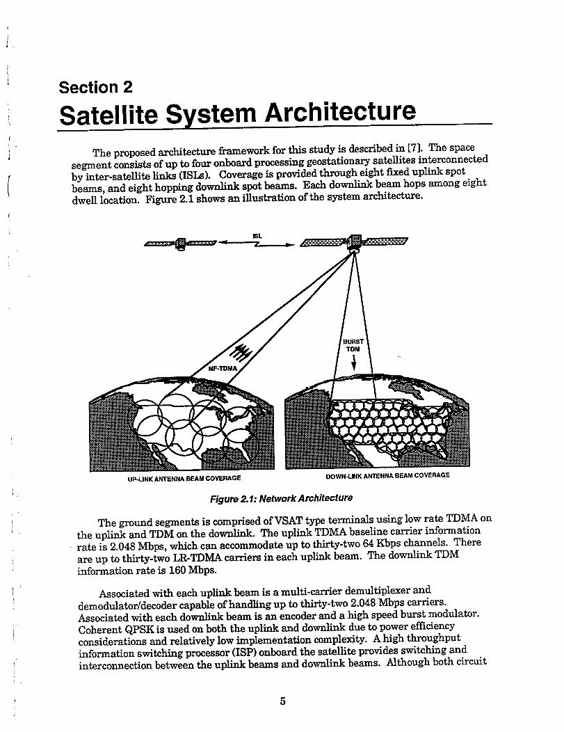
Satellite System ArchitectureThe proposed architecture framework for this study is described in [7]. The space
segment consists of up to four onboard processing geostationary satellites interconnected
by inter-satellite links (ISLs). Coverage is provided through eight fixed uplink spotbeams, and eight hopping downlink spot beams. Each downlink beam hops among eightdwell location. Figure 2.1 shows an illustration of the system architecture.
UP-LINK ANTENNA BEAM COVERAGE DOWN-LINK ANTENNA BEAM COVERAGE
Figure 2.1: Network ArchRecture
The ground segments is comprised of VSAT type terminals using low rate TDMA on
the uplink and TDM on the downlink. The uplink TDMA baseline carrier informationrate is 2.048 Mbps, which can accommodate up to thirty-two 64 Kbps channels. There
are up to thirty-two LR-TDMA carriers in each uplink beam. The downlink TDMinformation rate is 160 Mbps.
Associated with each uplink beam is a multi-carrier demultiplexer and
demodulator/decoder capable of handling up to thirty-two 2.048 Mbps carriers.Associated with each downlink beam is an encoder and a high speed burst modulator.
Coherent QPSK is used on both the nplink and downlink due to power efficiencyconsiderations and relatively low implementation complexity. A high throughput
information switching processor (ISP) onboard the satellite provides switching andinterconnection between the uplink beams and downlink beams. Although both circuit

and packet switching are being considered,the current architectureemploys a
destination-directedfastpacket switch design.
The current baseline packet format consists of fLxed length packets containing 2048
bits. Each packet is further divided into 16 subpackets, 128 bits each. The first
subpacket is the header subpacket which carries the packet routing information. The
remaining fLt_een subpackets carry the actual information payload along with some
parity check overhead.
In the current design,a packet istransmitted on the uplink in a 64 Kbps slotwithin
a singleTDMA frame. The TDMA frame length is32 ms, which isfurtherdivided intosixteen2-ms subframes. Each subframe contains one 128-bitsubpacket per channel, up
to thirty-twosubchannels. The firstsubframe within a frame carriesthe header
subpackets forthe respective32 channels which establishthe onboard routing
configurationforthat frame. The remaining fifteensubframes then carry the
information subpackets.
The downlink format consists of a 32-ms TDM frame which is divided among eight
downlink dwell time slots. The minimum dwell time is 80 microseconds which
corresponds to a minimum of 100 packets per dwell. A reference burst is included ineach frame for each dwell. The reference bursts could be transmitted either at the
beginning of the frame or at the beginning of each dwell in the frame.
The uplink and down]ink frame structure is shown in Figure 2.2., Table 2.1 provides
a summary of the system parameters in the current design.
_ UPLINK FRAME (32 ms) _ i
HEADER INFORMATION SUBPACKETSSUBPACKETS
I
I TS11 TS2 I TS3 I TS4 I .o. _-_
i '
SOURCE BITSDESTINATION BITS (51 bits)-_llm_j_ (19 bits)
IowE, .IFigure 2-_: Uplink and Downlink Frame Structure
6
\
)
1
]
l
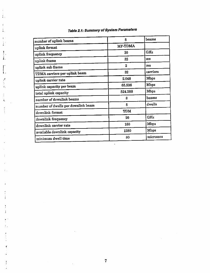
Table 2.1: Summary of System Parameters
m_mher of uplink beams
upJink format
uplink frequency
uplln_ fr.me
upl;nk sub frnme
TDMA carriers per uplink beam
up]_n_ c__trierrate
upl_n_capacityper beam
totaluplinkcapacity
n-tuberofdownlink beams
n-tuberofdwellsper downlink beam
downl_nk format
downlink frequency
downlink carrier rate
available downlink capacity
w_n_rnum dwell time
8
MF-TDMA
30
32
2
32
bean2s
GHz
ms
ms
icarriers
Mbps
Mbps
Mbps
beams
dwells
GHz
Mbps
Mbps
microsecs
2.048
65.536
524.288
8
8
TDM
20
160
1280
80
÷I
4"
7


Section 3
Alternative SynchronizationApproaches
tCoherent demodulation ofMF-TDMA carriersonboaerd the satelliterequires
synchronization ofcarrierphase and symbol timing between the received signalsand theonboard reference. Because ofthe TDMA nature ofthe uplink signalsin which several
terminals time-share the TDMA frame, synchronization isrequired for each terminal
transmission. There are a number ofapproaches to matching the carrierand timing
referencesto the received burst timing and carrier.These approaches can be categorized
under one ofthe following:
• conventional TDMA with preamble/unique word (UW), which would allow
derivationofcorrectburst timing from a preamble pattern
• conventional TDMA without preamble, which would involve storingand
demodulating the received burst in two passes,with interpolationofbittiming
• bitsynchronous TDMA with burst preamble, where the preamble pattern isonly
used to derive the carrier phase -,
• bit synchronous TDMA without burst preamble, with carrier phase estimationbased on the received burst data
The advantages of a bit synchronous approach is that it simplifies the demodulation
and demultiplexing onboard the satellite, and allows for a shorter (possibly zero-length)
preamble. A short preamble increases the TDMA frame efficiency, especially for shortdata bursts. Short data bursts are desirable in order to keep the TDMA frame length
short and hence minimize onboard storage and processing delay. The disadvantage of a
bit-synchronous system is that it adds some complexity to the ground segment.
The following sections describe each of the four approaches to TDMA
synchronization outlined above. All four approaches are based on burst synchronizationin which carrier and timing estimation is performed on each burst individually.
Continuos synchronization techniques in which carrier phase and symbol timingestimates are stored and tracked from one frame to the next are not considered to be
feasible due to the following reasons:
a. there may be significant changes in carrier phase and bit timing from one frame
to the next so that timing and phase coherence is not possible; or
b. earth stations do not necessarily transmit successive bursts in the same time slot
and at the same carrier frequency.

3.1 Conventional TDMA Synchronization
The first alternative considered in this study is a conventional TDMA approach in
which a preamble pattern is used to perform carrier recovery and bit timing recoveryover the preamble portion of the received burst. The preamble consists of a carrier and
bit timing recovery (CBR) pattern which generally includes an alternating bit pattern,
followed by a unique word pattern which is used for deriving the start of the data portionof a burst. Because burst timing may vary from one burst in a frame to the next, a guard
time must be allocated between bursts to prevent inter burst interference.
The onboard demodulator uses the CBR pattern to establish carrier phase and bit
timing estimates. It uses the unique word pattern to identify the start of the data
portion in the burst and to resolve any phase ambiguity in the carrier phase estimate.Once these estimates are calculated, they can be used to demodulate the information
portion of the burst or to initialize a digital phase lock loop which can track the phasevariations over the length of the burst. In general, if the frequency offsets between the
received carrier and the onboard reference are large enough to cause significant
variations in the phase over the length of the burst then some kind ofphase trackingmechanism must be used. However, if the frequency offsets are small enough, then the
phase estimates which are determined over the preamble can be used to demodulate the
entire burst.
A conventional TDMA approach usually utilizes QPSK modulation without any
need for differential encoding since the unique word pattern is used to resolve phase
ambiguity. A typical value of the preamble length is 96 symbols. Guard time between
bursts will depend on the accuracy of the user terminal clocks, and is generally a few
symbols long.
3.2 Preambleless TDMA Synchronization
In this approach, the earth station bursts are not synchronized with the satellite
clock, however no CBR pattern is included in the TDMA burst. Carrier and clock phaseestimates are derived from the received burst data patterns. This is usually done using a
two pass approach in which burst data is stored while it is used to obtain the bit timing
and phase estimates, then the recovered estimates are used to demodulate the storeddata. While this approach eliminates the preamble overhead, its shortfall is that it
requires a relatively long data sequence to derive a reliable timing estimate due to the socalled pattern noise. This imposes a limit on how short a data burst can be, and requires
enough additional onboard storage for performing the two pass demodulation.
Bit timing estimates can be derived from the received data independently of the
carrier phase by using the algorithm outlined in [8]. Carrier phase can be derived from
the data using a nonlinear phase estimation algorithm [9] if bit timing is known. The
phase estimation algorithm can generally yield reliable estimates over a few symbols
provided there are no significantly large frequency offsets.
Due to the absence of a preamble pattern to resolve phase ambiguity, this
alternative will generally utilize deferentially encoded QPSK. DQPSK exhibits twice the
9
1
l
l
I
I

tl
i .
bit error rate of QPSK, however the doubling in the bit error rate translates to only a
slight degradation in the required signal to noise ratio.
As with the conventional TDMA approach, this approach will require a guard time
between consecutive bursts to absorb any differences in burst timing between user
terminals.
3.3 Bit Synchronous TDMA with Preamble
In bit synchronous TDMA, system timing is maintained so that all transmissions
arrive at the satellite synchronized to the same clock. This symbol synchronous systemalso allows frame synchronization and burst synchronization, thus eliminating the need
for guard time between bursts and eliminating the requirement for a unique word
pattern to identify the start of the burst. A description of the overall concept of bit
synchronous operation is given in the following subsection.
If desired, a carrier synchronization pattern can be used to obtain a carrier phase
estimate, as in the conventional TDMA system. However, the preamble length will
generally be less than it would be in an asynchronous system since reliable carrier phaseestimation requirements are generally less stringent than the bit timing estimation
requirements.
The preferred modulation format for this alternative is coherent QPSK. Becauseburst timing is known, the alternating pattern used for carrier recovery can also be used
for phase ambiguity resolution so there will be no need for deferential encoding.°
3.4 Preambleless Bit Synchronous TDMA
In bit synchronous TDMA, bit timing is maintained by controlling the transmitterminal timing in such a way as to have all transmissions arrive at the satellite in a bit
synchronous fashion. This implies that some form of bit timing adjustment must be
implemented at the transmit terminal based on the difference in bit timing at the
satellite between the onboard clock and the received burst.
User terminal clock correction is generally done by making bit timing errormeasurements onboard the satellite and relaying those measurements back to the
transmit terminal. The user terminal implements some form of local clock correction
based on the received feedback from the satellite. The feedback information from the
satellite can be either an early / late type of signal or could include more information on
the desired value of timing correction. Other methods of ensuring bit synchronous
timing at the satellite include precision ranging or self monitoring of the received signals,however these methods will generally require some guard time between bursts to absorb
any timing uncertainties and are only practical for very low rate transmissions.
With bit synchronous operation, carrier phase estimation can be performed on the
TDMA data burst using the Viterbi and Viterbi algorithm [9] which is capable of
producing fairly reliable phase estimates based on a small number of symbols in thereceived data pattern. This algorithm has been shown to be very well suited for use in a
10

low-rate TDMA (LR-TDMA) bitsynchronous system [10]similarto the one being
considered in thisstudy.
3.4.1 Bit Timing Accuracy
Burst timing in a bitsynchronous system must be accurate to within a small fraction
ofa symbol time. To get an idea ofthe performance sensitivityto bittiming inaccuracies,
a simplifiedanalysisofnon-filteredcoherent QPSK isperformed as shown in Figure 3.1.
Using an integrate-and-dump filteron a rectangular pulse,the performance degradation
isgiven by
E_, Pb(T_-2At) 2At E b
No
Table 3.1 shows the expected degradation in performance based on the above
equation for(non-filtered)coherent QPSK as a function ofstaticbit timing error. From
Table 3.1,itisevident that a 5 % (or 1/20)timing error forexample would provide
adequate performance within 0.5 dB from theoretical.In order to achieve a required bit
timing accuracy,a capabilityto accurately measure bittiming errorson board the
satelliteisrequired,as well as a capabilityto accurately correctthe transmit terminal
timing towithin the required accuracy.
Figure 3.1: Performance Degradation Caused by Symbol Timing Error
3.4.2 User Terminal 2Yming Control
In order to achieve the required timing accuracy, two steps are required at the user
terminal. The first step involves initial timing acquisition which is performed by sending
an acquisition burst in a specified time slot (channel) on an assigned TDMA carrier. The
acquisition burst contains a preamble pattern to allow precise measurement of symbol
timing onboard the satellite. Due to the initial timing uncertainty, the acquisition time
slot also includes a guard time long enough to absorb the timing uncertainty. Based on
the acquisition burst timing measurement a timing correction signal is sent back from
the onboard processor to the ground terminal specifying the timing offset in symbols as
11
L
1
t

Table 3.1: Degradation in SNR vs. Static Timing Error
Phase Error
ATJTs
O%
1%
2%
3%
4%
5%
6%
7%
8%
9%
10%
Degradation
(dB)
0.00
0.09
0.18
0.27
0.36
0.46
0.56
0.66
0.76
0.86
0.97
well as in fractions of a symbol. The ground terminal corrects its timin" g and sends
another acquisition burst. This process is repeated until the correct timing (to within a
specified tolerance) is reached and acknowledged by the onboard processor. Once aterminal has acquired the correct bit timing, sync21ronization is maintained by
performing periodic corrections in fractions of a symbol, based on bit timing errormeasurements. In general, these measurements are performed by the onboard processor
on a special synchronization burst which is transmitted periodically by the groundterminal. Figure 3.2 illustrates the concept of bit synchronous timing corrections using
onboard timing error measurements.
As mentioned above, bit timing measurements onboard the satellite can be made on
a special synchronization burst that each transmit terminal sends in turn in a specified
synchronization time slot in the TDMA frame. The frequency of these measurements,and hence the frequency of transmitting the synchronization burst for each terminal
depends on several factors such as the stability of the onboard and terminal clocks, thesatellite motion Doppler, and other factors such as the method used to derive the ground
terminal timing. Section 6 of this report, which deals with timing analysis for bit
synchronous system, addresses the frequency with which these corrections should bemade. It should be noted here however that these are fine timing adjustments that are
made after initial course timing acquisition is made, including burst timing and symbol
timing acquisition.
12

4 TRANSMITPROCESSOR
Ale
TX TIMINGCORRECTION
RECEIVEPROCESSOR
DOPPLER: Z_.
DOPPLER:Af de
OBP bit timing : ;ample poim
BASEBANDPROCESSOR
ON-BOARDA_ REFERENCECLOCK
Figure 3.2: Bit Synchronous Concept
3.4.30nboard Timing Measurements
To allow accurate bit timing measurements onboard the satellite, the timing
synchronization (or timing maintenance) burst will consist of a special sequenceconsisting of alternating pairs of identical symbols. This in effect halves the received
symbol rate for the synchronization burst, which effectively doubles the onboard
sampling rate. With the higher sampling rate, accurate timing error measurements are
made by an onboard timing error measurement processor. A more detailed analysis of
the timing error measurement technique will be given in subsection 4.3.
3.50nboard Hardware Tradeoffs
The advantages of using bit synchronous TDMA in terms of onboard processing is
derived mainly in the demultiplexing and demodulation process, especially for multi-
carrier demultiplexing/demodulation.
From an onboard demodulation standpoint, when symbol timing is known on a burst
by burst basis, the demodulator could operate at the symbol rate. Where as in aconventional TDMA system, the demodulator would operate at or above the Nyquist
sampling rate of the demultiplexed carriers. This is at best higher than the symbol rate
13
I
i)
"/
,l
]
]
]

i_
by the roUofffactorofthe pulse shaping filter,which would generally be from thirtyto
fiftypercent. Itisnot uncommon to have the demodulator operating a twice the symbol
rate,which isa factorofone-hundred percent higher than the symbol rate. In a bit
synchronous system where the sampling rate could be atthe symbol rate,the samplingrate reduction translatesintosavings in mass and/or power.
Another advantage of bitsynchronous operation in terms ofonboard demodulation is
the eliminationofthe bittiming recovery process. In conventional (asynchronous)
TDMA, bittiming recovery has to be performed on the receiveburst,which entailseither
the addition ofa bittiming recovery pattern tothe preamble, or storingthe burst (orpart
of the burst)and derivinga bittiming estimate from the stored samples before doing the
demodulation in a second pass. Both approaches may be wasteful ofresources. The first
approach requires a bittiming recovery pattern which increases the burst preamble
overhead. The second approach involvesstoringenough data to allow reliableestimation
ofthe receivedbittiming. Since bittiming isusually derived from the zerocrossing of
the receivedwaveform, and since forfilteredQPSK the zerocrossings depend on the
pattern noise (ISI)at the zero crossinginstantwhich isnot null even in the absence of
thermal noise,a reliableestimate may require a long averaging intervalover which
many zerocrossingsare averaged. This added processing alsotranslates intoonboard
mass and power increases.
Related tothe increase in processing requirements and burst overhead in a
conventional (asynchronous) TDMA system isthe correctionofbittiming once an
estimate ofthe bittiming ismade. This involves an interpolationfilterforthe received
samples which isused to interpolatethe sample value ofthe received signalat the
sampling instant. An alternativefora system with a long bittiming recovery pattern is
to adjustthe sampling point over the data portimi ofthe burst based on the bittiming
estimate derived during the bittiming preamble pattern. Both approaches involve added
complexity and reduced flexibility,especiallyin the implementation of an onboard multi-
carrierdemodulator.
Finally,multicarrierdemultiplexing can be made simpler when only a singlesample
per symbol isrequired at the output ofthe demultiplexer (as in a bitsynchronous
operation).This alsotranslatesto mass and power savings over conventional TDMA.
Section 4 ofthisreport deals specificallywith the impact of bitsynchronous
operationon the onboard hardware, including mass and power estimates and
comparisons.
!
i
3.6 Frame Efficiency Tradeoffs
The elimination of burst preamble in a bit synchronous system results in high frame
efficiency which is crucial for short burst length. From another viewpoint, elimination of
burst preamble allows much shorter bursts for a given frame efficiency. Figure 3.3
illustrates a bit synchronous TDMA frame and compares the required burst overhead
with that of conventional TDMA bursts.
14

/
TDMA FRAMF l_ iI
.-c i -- i -c l-cl ,-,c iSLOT BURSTA BURSTB BURSTC BURSTD
_°'_.0°"°_"-0. • il_I"i_ _/.rr O.T. [NJII
SYNCHRONOUS I:._1
__._:_:__'_:'_""_'_"_ ..........'_'__ I::"::";::::_:_'_":::::::::"::__ii_! __:_:_::_::Si:_'::
l;_._l_'.-"._!_:_-:Yi*"l -i_i_'-_|_|..........................
Figure 3.3: Bit Synchronous TDMA Frame
A quantitative comparison between the bit synchronous TDMA approach and theconventional TDMA approach is shown in Table 3.2. In this comparison, frame length is
calculated based on the required frame efficiency for a given number 0fbursts per frame.The results show the sizable difference in the required frame length between the
conventional TDMA approach and the bit synchronous approach.°
The tradeoffs given in Table 3.2 focus on the required TDMA frame length for a
given frame efficiency. In the current system design however, the frame length is fixedat 2 ms (subframe duration) with a subburst length of 128 symbols. In such a system,
the preamble length of 96 symbols assumed in Table 3.2 plus all other overhead termsincluded in the comparison, would result in a frame efficiency which is less than 50 %.
Hence, the elimination of burst preamble in the current system design is even more
critical in terms of frame efficiency compared to the cases considered in Table 3.2.
15
_]
Ii
if
:I
i
.I
_I
I

i
i
it
Table 3.2: TDMA Frame Length Comparison
Transmission: QPSK UW: 24 symInformation Rate: 2.048 Mbps Post Amble: 8 sym
Acquisition Window: 80 ps Acq/Synch: 128 symGuard Time: 8 sym SCPB Header: 40 sym
CBTR: 96 sym
Non-Bit Sync.
Frame Length
(ms)
Bit Sync TDMA
Frame Length
(ms)
Conventional TDMA
Ratio of Frame
Length
Frame No. of Bursts/Frame
Effic. 20 40 60 80 100
70% 2.5 4.8 7.1 9.3 11.6
75% 3.0 5.8 8.5 11.2 13.9
80% 3.8 7.2 10.6 14.0 17.4
85% 5.1 9.6 14.1 18.7 23.2
90% 7.6 14.4 21.2 28.0 34.8
95% 15.2 28.8 42.4 56.0 69.6
70% 0.4 0.5 0.7 0.8 0.9
75% 0.5 0.6 0.8 1.0 1.1
80% 0.6 0.8 1.0 1.2 1.4
85% 0.8 1.1 1.3 1.6 1.9
90% 1.2 1.6 2.0 2.4 2.8°
95% 2.4 3.2 4.0 4.8 5.6
6.3 9.0 10.6 11.7 12.4
i
Single Channel Per Burst
No. of Bursts/Frame
20 40 60 80 100
12.0 15.0
14.4 18.0
18.1 22.5
24.1 29.9
36.1 44.9
72.2 89.8
3.5 4.3
4.2 5.2
5.3 6.5
7.0 8.6
10.5 12.9
21.0 25.8
3.2 6.2 9.1
3.9 7.4 10.9
4.9 9.3 13.7
6.5 12.3 18.2
9.7 18.5 27.3
19.4 37.0 54.6
1.1 1.9 2.7
1.3 2.3 3.2
1.7 2.9 4.1
2.2 3.8 5.4
3.3 5.7 8.1
6.6 11.4 16.2
2.9 3.2 3.4 3.4 3.5
3.7 Summary Comparisons
In conclusion, Table 3.3 summarizes the salient features of each of the four
approaches to TDMA synchronization described above. In Table 3.3, the term'conventional TDMA' is used to refer to a non-bit synchronous TDMA system.
Based on the comparisons in Table 3.3, the bit synchronous approach to TDMA
synchronization is selected for further study. Further evaluation of the impact of this
approach on onboard hardware will be given in the next section.
16

Table 3.3: TDMA Synchronization Summary Comparisons
preambleoverhead
guard timeoverhead
timing recoveryrequired
tight groundtiming control
shortbursts
possible
onboard hardware
complexity
added groundterminal
complexity
optionA
ConventionalTDMA (withPreamble)
yes
yes
yes
no
no (limited byratio of data tooverhead)
more complex
none
option B
Conventional
TDMA (noPreamble)
no
yes
yes
no
no (limitedby
datasymbols
requiredfor
timingrecovery)
most complex
none
option C
Bit SynchronousTDMA (withPreamble)
yes (less)
no
no
yes
iyes (although stilllimited by ratioof data to
preambleoverhead)
simplest
some
optionD
Bit SynchronousTDMA (noPreamble)
no
no
no
yes
!yes
simpler
some
17
ill
I

Section 4
Impact on Onboard Demultiplexingand Demodulation
This section addresses the impact on onboard hardware of each of the TDMA
synchronization options presented in section 3. Qualitative and quantitativecomparisons of mass, power, and complexity, are made between the four optionsconsidered. The section also addresses onboard timing error measurements which is
relevant for bit synchronous systems.
4.10nboard Demultiplexing
Onboard demultiplexing complexity is affected by several factors which may differ
between bit synchronous and asynchronous TDMA. These include the bandwidth to
symbol rate ratio, the number of samples per symbol required at the demultiplexer
output, and the interpolation requirement following demultiplexing to obtain samples at
the correct time instant.
In order to obtain meaningful comparisons between the two approaches, a
demultiplexer algorithm and general architecture is first presented. Based on the
proposed architecture, several cases which are applicable to bit synchronous andconventional TDMA are considered. Demultiplexer and interpolation filter complexity is
addressed and mass and power estimates are then obtained for representative cases.
7
t
f
4.1.1 Demultiplexer Algorithm and Architecture
Demultiplexing uniformly loaded frequency bands, as in a MF-TDMA system, is
considerably simpler than demultiplexing a flexibleregion. Indeed, itiswell known that
fordemultiplexing uniform bands the approach known as polyphase isthe least
computationally intensive,and hence the preferredchoice[11].This approach issimilar
to that used in digitaltrausmultiplexerswhere a group of frequency-divisionmultiplexed
(FDM) channels are transformed to time-divisionmultiplexed (TDM) channels (and vice
versa). The similarityliesin the signalprocessing techniques used toperform the
frequency demultiplexing. COMSAT isthoroughly familiarwith allthe detailsofthis
approach, having designed and builta 60-channel polyphase transmultiplexer [12].
The polyphase approach takes fulladvantage ofthe factthat the differentselective
bandpass filtersneeded forthe demultiplexing are equally spaced frequency replicasof a
baseband prototype. Thus, thisapproach isideallysuitedto applicationswhere all
carriershave the same allocatedbandwidth B. Figure 4.1 illustratesthe various
bandpass filtersneeded todemultiplex a uniformly loaded band as exact replicasofthe
baseband prototype Ho. (H willbe used to denote a filter'sfrequency response, and h will
denote itsimpulse response).
18
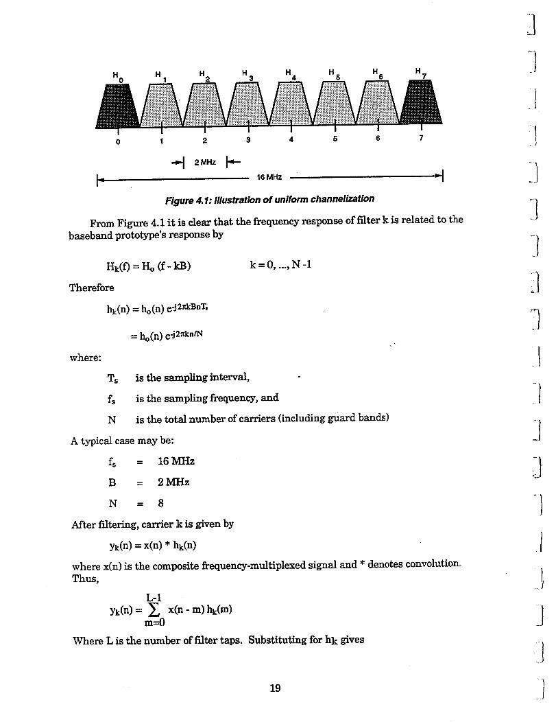
H H0
It:H2 H 3 H 4 H
2 3 4
5 H6 H7
I
5 6 7
2 MHz I_--
16 MHz r I
Figure 4.1: Illustration of uniform channelization
From Figure 4.1 itisclearthat the frequency response offilterk isrelatedto the
baseband prototype'sresponse by
Hk(f ) = H o (f- kB)
Therefore
hk(n)= ho(n)c"j2r_kBnT=
= ho(n)e'J2nknm
where:
Ts
fs
N
A typicalcase may be:
fs = 16 MHz
B = 2 MHz
N = 8
After filtering, carrier k is given by
yk(n)= x(n)* hk(n)
k=0 ....,N-I
isthe sampling interval,
isthe sampling frequency, and
isthe totalnumber ofcarriers(includingguard bands)
where x(n) is the composite frequency-multiplexed signal and * denotes convolution.
Thus,
L-1
yk(n) = Z x(n -m) hk(m)m---0
Where L isthe number offiltertaps. Substituting forhk gives
19
:/
:]
]
_]
]
J
l

I
i
f
| _
L-1
yk(n)=
m---0
x(n -m) ho(m) c-J2ram#N
For the square rootraisedcosine filters,the impulse response must be truncated
afteran appropriatenmnber ofsymbols. Computer simulations and actualmeasurements at COMSAT Laboratories have shown that negligibledegradation results
when the extent ofthe impulse response islimited tofivesymbols in the 50-percent
rolloffcase.Therefore,the number offiltertaps,L, isgiven by
W
L=5_s-5T'N'B
where T isthe symbol duration;thus,
L=7.5N
To simplifythe implementation, the slightlylargervalue of8N willbe taken forL. By
writing
L=N°Ns
itfollowsthat
Ns=8
Substituting for L gives
(N. Ns}-I
yk(n)= Z x(n -m) ho(m) e-j2nkm/N
m=0
To reduce the above expression foryk(n) to a form involving a discreteFourier transform
(and hence use the efficientFFT algorithm),the index m iswritten as
m=Noi+r i=0 ...., Ns- 1
r=0,...,N- 1
Therefore,
Ns-1 N-1
yk(n)= Z Z x(n- S •i-r)ho(N •i+ r)•e-j2nkr/N
i=O r=O
where use was made of the identity
e-j2xkN ° i/N = 1
Interchanging the order of summations gives,
20

N-1 rNs-1 r)1yk(n) = _ e'J2=krm / _ x(n- N-i-r) ho(N-i +r=-0 L i--0
Defining
Ns, l
Zn(r) =i--0
x(n- N.i-r)ho(N.i+r)
gives
N-I
yk(n)= _ e'j2r'_r_zn(r)r=O
This last expression simply says that yk(n) is the N-point discrete Fourier transform
of zn(r). The relation between the quantities x, y, and z is illustrated in Figure 4.2.
POLYPHASEFILTER COEFFS
x lI
Signal
h0
PRESUMMING zII I I I
N . N Samples N SamplesS
N-POINTFFT
Y_
DemulUplexed
Output; 1 TimeSample for Eachof N Channels
I IN Samples
Figure 4.2: High level block diagram of polyphase filter
Note that the result of the Fourier transform is
yo(n), yl(n) .... YN-l(n)
that is, all values are obtained for a fixed time n, one value for each carrier k.
To summarize, the 16-MHz signal x is fed to a digital presumming filter to obtain
the intermediate signal z, as given by the equation for z above. The 16-MHz signal z is
then input to an 8-point FFT. The output eight points represent one point for each
21
I• /
1
I
I
3
J
:]

i
carrier (six actual carriers plus two guard bands). The output signals are thus sampled
at 2 MHz each.
A proposed implementation of the presummer using four ASIC chips is shown in
Figure 4.3. When used in this combination, the ASIC chips compute the quantity z from
the input values x according to the equation for z above. The sequence z is computed in
the following order:
zn(r), zn(r-1), zn(r-2), ..., zn(r-7), zn + s(r), zn + s(r-1), zn + s(r-2), ..., Zn+ s(r-7) ....
This sequence is readily obtained from the serial stream x fed to the shii_ registers
by setting the variable delays between the register stages to seven samples each. At eachclock, a new set of coefficients is loaded into the ASICs, with the coefficients repeating
after eight clocks. Each set of 8 values for z with the same subscript, n, constitute the
input to the 8-point FFT that follows the presummer, as described above.
o.T/-
c_m_._P_ . / //_ -
I COomfp_nent
,_°_z r'
ata Out
Register
DataOut
Q Component
o1X
Q Coloponentof Z
Figure 4.3: Block diagram of polyphase presummer
4.1.2 Cases Considered
Four separate cases are considered below to cover the range of options of interest as
far as the filtering operations are concerned. These cases are as follows:
A) B = 2 Rs, Demux output 2 s/s
Here the carriers are spaced by twice the symbol rate. The demultiplexer produces 2
samples per symbol at its output. For an asynchronous network, the demultiplexer may
22

be followed by an interpolationfilterand a demodulator, or alternativelythe
interpolationfiltermay be removed and a demodulator operating directlyon the
asynchronous samples may be used [13].For a synchronous network, the samples atthe
demultiplexer output have the desiredphase relationtothe symbol, and hence a simple
demodulator isused.
B) B = 2 Rs, Demux output i s/s
Here the carriersare spaced as in A) above, but the demultiplexer only produces 1
sample per symbol at the output. This resultsin reducing the power requirement ofthe
demultiplexer to approximately halfitsvalue in A) above. However, sinceonly i sample
isproduced per symbol, thiscase isonly applicableto a synchronous network.
C) B = 1.5Rs, Demux output 1.5 s/s
Here the carriersare spaced by 1.5 times the symbol rate. In addition to the
bandwidth savings (which may or may not be important),the demultiplexer power
requirements are alsoreduced sincethe sampling frequency isnow reduced compared to
A) and B) above. As in A), severalpossibilitiesexistforthe demodulator.
D) B = 1.5 Rs, Demux output 2 s/s
In thiscase,the carriersare spaced by 1.5 times the symbol rate,but the
demultiplexer output is2 samples per symbol. This resultsin increased complexity in
the demultiplexer compared to C) above. On the other hand, the demodulator and
interpolatingfilter,if any, are simpler.
4.1.3 Polyphase Demultiplexer and InterpolationFilterComplexity
The four cases denoted by A, B, C, D above are ofparticularinterest.The
complexity ofthe multiplexer in each case isdetermined primarily by the desired output
rate,assuming that the number ofcarriersisthe same in allcases. This isattributed to
the factthat the polyphase FFT, as well as the multipliersand adders in the polyphase
summer operate at the output sampling rate. Therefore, cases A and D are the most
power consuming forthe demultiplexer,with case B consuming about halfthe power, and
case C 75% ofthe power ofcases A and D.
When used, the interpolation filter contributes significantly to the processor
complexity. The filter has an FIR structure with an impulse response that is constantly
sliding to satisfy the desired phase relationship between input and output samples. Tomake matters more difficult, this filter should be shared among several carriers to avoid
duplication of hardware.
Two cases are ofparticularinterest.In the firstcase,the input sampling rate of
each carrieris1.5 Rs and in the second, itis2 Rs. The output in both cases is2Rs. Note
that in the second case,the number ofinput samples equals the number of output
samples, and only the relativepositionofthose samples within a symbol differ.(The
output samples are desired at mid-symbols and symbol edges.) •
23
1
41
iI

i
|.
The complexity of the interpolation filter is approximately the same in these 2 cases,
since it tends to be dominated by the number crunching requirement which is itself
determined by the output sample rate. The slight simplifications afforded by the lower
input sampling rate of 1.5 Rs are offset by the slightly larger control complexity in that
case.
4.1.4 Power and Mass Estimates
The power and mass estimates given below are very preliminary, but are helpful in
performing tradeoffs between various configurations.
The following benchmarks can be used in estimating the power requirement for the
polyphase demultiplexer. For 32 channels, and a sampling frequency of 20 MHz, thepolyphase demultiplexer would require approximately 2 watts. The FFT chip and the
summer chip would have roughly equal contributions to the power. These numbers arebased on CMOS radiation hard technology with a power figure of 2 microwatts per gate
per MHz. For different sampling frequencies, the scaling should be linear.
Note that it is the aggregate output frequency that impacts the power requirement
most directly,sinceitdetermines the rate atwhich the number crunching operations
must take place. The scalingwith the number ofchannels isapproximately logarithmic.
With these benchmarks, one can obtain a rough estimate ofthe demultiplexer power
requirements for different configurations and parameter values. .
Similar approximate estimates can be obtained for the interpolation filter. The
complexity of this FIR filter is dominated by the multiplier requirements, as roughly halfthe total interpolation power goes into the multipliers. A one point estimate of the power
required indicates that an interpolation filter chip shared among 16 carriers, running at20 MHz would require about 1 watt of power, again assuming CMOS radiation hard
technology with a power figure of 2 microwatts per gate per MHz. Again the scaling with
the speed is roughly linear, and with the number of carriers roughly logarithmic.
Mass estimates, at this preliminary stage, can be obtained by using extrapolations
from similar digital technology developments. Previous experience indicates that for
similar developments, approximately 7.5 W of power correspond to 1 kg of mass. Using
this correspondance, an overall mass estimate is quickly obtained once an overall power
estimate is computed.
f
4.1.5 Example
As an example of the approximate estimation procedure of power and mass outlined
above, consider 16 frequency multiplexed carriers of I Msymbol per second each (12actual carriers and 4 guard bands). The estimates for power and mass of the
demultiplexer and interpolation filter (if used) are given below for the 4 cases considered.
24

A) B = 2 Rs, Demux output 2 s/s
Sampling frequency = 16 B = 32 MI-IzPower for demultiplexer = 2.5 watts
Mass for demultiplexer = 0.33 kg
Power for interpolation filter = 1.2 watts
Mass for interpolation filter = 0.16 kg
B) B = 2 Rs, Demux output I s/s
Sampling frequency = 16 B/2 = 16 MHz
Power for demultiplexer = 1.25 watts
Mass for demultiplexer = 0.17 kg
C) B = 1.5 Rs, DemuI output 1.5 s/s
Sampling frequency = 16 B = 24 MHz
Power for demultiplexer = 2 watts
Mass for demultiplexer = 0.25 kg
Power for interpolation filter = 1.2 watts
Mass for interpolation filter = 0.16 kg
D) B -- 1.5 Rs, Demux output 2 s/s
Sampling frequency = 16 B x 4/3 = 32 MHzPower for demultiplexer = 2.5 watts
Mass for demultiplexer = 0.33 kg
Power for interpolation filter = 1.2 watts
Mass for interpolation filter = 0.16 kg
4.20nboard Demodulation
4.2.1
Onboard demodulator complexity is generally somewhat lower than the onbeard
demultiplexer complexity, especially for "well behaved" AWGN channels which do not
suffer from multipath fading and large frequency offsets. This is due to the
computationally intensive nature of demultiplexing inherent in digital filtering
operations. Nevertheless, onboard demodulator complexity is still critical since it
translates directly into how many carriers at a given rate can be demodulated using a
single chip.
Onboard Demodulator Operation
Demodulator complexity isgenerallydetermined by whether or not the following
operations are performed by the demodulator, and the manner in which they are
performed:
25
• l
1. /
)

i
I_
i
• unique word detection
• carrier synchronization
• symbol timing synchronization
• sample interpolation
• detection
The four TDMA synchronization options being considered will have different
requirements on each of the above functions.
Conventional TDMA (option 1) requires unique word detection, carrier and symbol
timing synchronization, and detection. Unique word detection and carrier and timing
synchronization are done in real time over the preamble portion of the burst as theTDMA burst isbeing received. Detection is alsodone in realtime aftersynchronization
using the carrierphase and timing referencederived from the preamble pattern.
Preambleless (asynchronous) TDMA (option2)demodulation alsorequires unique
word detection,carrierand bittiming estimation,and detection.However, carrierand
bittiming estimation isperformed on the data portion ofthe burst. This involves storing
the receivedburst fortwo pass demodulation, in which detectionisdone in a second pass
aftercarrierphase and timing estimates are obtained. In addition,sample interpolation
is required for detection based on the timing estimates. ::
Bit synchronous TDMA demodulation on the_other hand only requires carrier
synchronization and detection. Carrier synchronization can be performed in realtime on
a short preamble pattern (option3),or can be estimated using a small portion ofthe
burst data ifthe burst does not include a preamble pattern (option4). In the lattercase,
a few data symbols willhave to be storedto get the phase estimate before detectioncan
be done.
4.2.2 Demodulator comparisons
Based on the above discussion, demodulator complexity comparisons can be made
among the four synchronization options being considered.
Option 3 (bit synchronous with preamble) is by far the least complex from anonboard demodulation standpoint and will be assigned a relative complexity value of 1.
Option 4 (preambleless bit synchronous) is slightly more complex since it involves
carrier phase estimation based on the random data in the received burst (e.g. usingViterbi and Viterbi algorithm [9]). This added complexity however is minimal and will
have little impact on the comparisons. Therefore this option is also assigned a relative
complexity value of 1.
26
Option 1 (conventional TDMA) is more complex in terms of onboard demodulation
since it requires unique word detection, as well as carrier phase and timing
synchronization. This option is assigned a relative complexity value of 2.
Finally, option 2 (preambleless asynchronous TDMA) is the most complex from the
onboard demodulation standpoint since it requires all the above demodulation functions.
In addition, demodulation and detection is performed in a two pass approach whichinvolves onboard storage and sample interpolation. This option is assigned a relative
complexity value of 4.
4.2.3 Mass and Power Estimates
Based on the comparisons in the previous subsection, mass and power estimate: :_
shown in Table 4.1 for each one of the four TDMA options considered. Power estima'. :
assume I watt per chip. Mass estimates are based on 1 Kg to 7.5 watts of power. Thenumber of carriers per chip is based on 1 Msym/sec carrier rate. All estimates scale
linearly with symbol rate and number of carriers.
relative complex.
carriers/chip
32 carriers power
8 x 32 cart. power
8 x 32 carr. mass
Table 4.1: Demodulator Power and Mass Estimates
Option 1
2
8
4W
32W
4.26 Kg
Option 2
4
4°
8W
64W
8.52 Kg
Option 3
1
16
2W
16 W
2.13 Kg
Option 4
1
16
2W
16W
2.13 Kg
In the above table, the last two rows represents the overall estimates of demodulator
power and mass for the entire system assuming 8 uplink beams with 32 carriers per
beam.
4.30nboard Timing Error Measurement
The above comparisons have shown the impact of bit synchronous operation on
onboard demultiplexing and demodulation in terms of complexity, mass, and power.
Another impact of bit synchronous TDMA on onboard hardware is the requirement of
onboard error measurements. This subsection examines onboard timing error
measurements.
27
iii
"''!
. t
)A

4.3.1 Error Measurement Technique
Onboard timing error measurements have to be performed on user terminal
acquisition and synchronization bursts to determine timing phase error. However, sincethe onboard demultiplexers operate with one output sample per symbol, these
measurements can not be performed at the symbol rate Rs.
An onboard timing error measurement technique is shown in Figure 4.4. In this
technique, the user terminal acquisitionand synchronization bursts consistof an
alternatingpattern of symbol pairs which effectivelyhalves the symbol rate. Thetransmitted filteredpattern consistsoftwo tones as shown in Figure 4.4 at Rs and Rs/2.
The onboard acquisitionand synchronization processoreffectivelyfiltersout the Rs
component and performs timing estimation at halfthe symbol rate (two samples per
symbol) as shown in the figure.
x
DigitalFilter t
Y2 x ArcTan _--
Rs f I Rs t V
Figure 4.4: Timing Error Measurement Technique'
The phase error measurement process isaffectedby two main sources ofinaccuracy.These are thermal noise and quantization noise. Itisgenerallydesirableto keep the
inaccuracy to within i% of a symbol duration. Thermal noise isgenerally the dominant
source ofinaccuracy provided there isa reasonable number ofqantizationlevelsare used
(e.g.8-bitquantization).Narrow band filteringofRs/2 component alsoyieldssome
improvement in the signalto noise ratiofortiming estimation in proportion tothe filter
bandwidth. The next subsection presents an analysisofthe timing error measurement.
4.3.2 Equation forTiming Measurement Error
The phase error ofan uplink signalrelativeto an onboard clockisgiven by
T 28

where Yl and Y2 are values of a clock signal sampled at times 0 and _2. The major
causes of phase measurement error are quantization noise and uplink noise. Since these
terms are generally small compared with a signal component, the above equation may be
expressed in the following form:
O=eo+Ae
where e0 and Ae are respectivelyan actualphase and measurement error and are related
to Yl and Y2 as follows:
yi=ylo+AYl
Y2 = Y2o + AY2
00_.Yl0 J
jA sinusoidaltiming signalwith noise isexpressed in the followingform:
where cos= 2_ /Ts isan angular frequency and T_sisa symbol period. The value ofy(t)
afterquantization isYl and y2 at t=Ts and t=0:
Yi = A+Ayqz+n(tl )
Y2 = OoA+ Ayq2 + n(t2)
where Ayql and Ayq2 are quautization errors. Simple calculationshows that the
standard deviationof Ae isgiven by the followingexpression:
For n-bitquantization
1 1
oq=_- 2-_
i
On =_
29
]
_J
]
1
.J
]
]
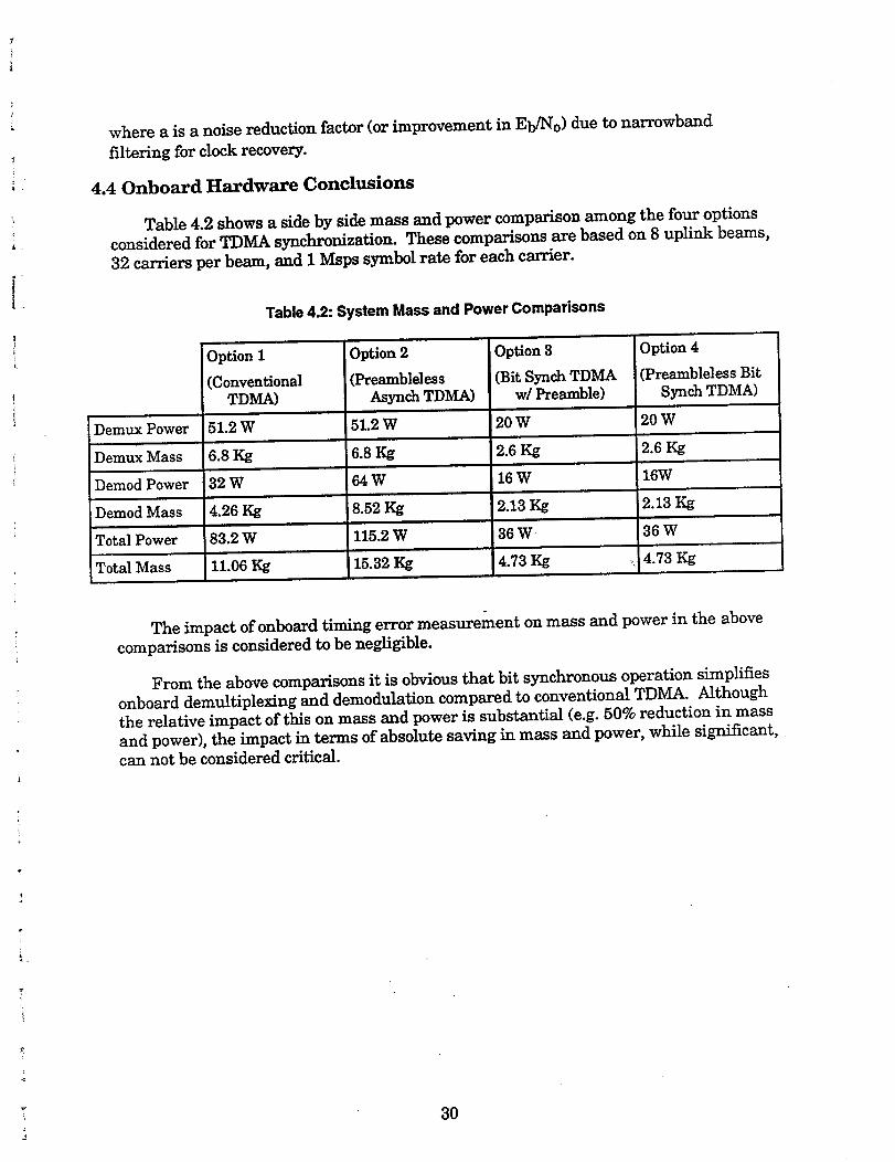
where a isa noise reductionfactor(orimprovement in Eb/No) due to narrowband
filteringforclockrecovery.
4.40nboard Hardware Conclusions
Table 4.2 shows a sideby sidemass and power comparison among the four options
considered for TDMA synchronization. These comparisons are based on 8 uplink beams,
32 carriersper beam, and 1 Msps symbol rate foreach carrier.
Table 4.2: System Mass and Power Comparisons
Demux Power
!Demux Mass
Demod Power
Demod M_s
Total Power
TotalMass
Option 1
(Conventional
TDMA)
51_2 W
6.8KS
32 W
4.26 Kg
i83.2 W
11.06 Kg
Option 2
(Preambleless
Asynch TDMA)
64 W
8.52 Kg
115.2 W
15.32 Kg
Option3
(BitSynch TDMAw/Preamble)
20 W
2.6KS
16 W
4.73 Kg
Option 4
(Preambleless BitSynch TDMA)
20 W
2.6KS
16W
2.13 KS
36 W
4.73 KS
The impact of onboard timing error measurement on mass and power in the above
comparisons is considered to be negligible.
From the above comparisons it is obvious that bit synchronous operation simplifies
onboard demultiplexing and demodulation compared to conventional TDMA. Although
the relative impact of this on mass and power is substantial (e.g. 50% reduction in mass
and power), the impact in terms of absolute saving in mass and power, while significant,
can not be considered critical.
3O

f , L )

1 .
Section 5
Ground Terminal Timing CorrectionTechniques
This section examines methods for deriving and correcting ground terminal transmit
timing so that it closely tracks onboard reference timing. It addresses alternate sources
of ground terminal timing and timing correction techniques which are applicable for
synchronization of the transmit clock to the onboard clock after initial timing acquisition
has been performed.
5.1 Timing Issues
For a bit synchronous system to operate properly, the ground terminal transmit
timing should closely track the onboard reference timing to within a small fraction of a
symbol (typically 5%). This requires initial timing acquisition over which the groundterminal adjusts its timing over a number of symbols and fraction of a symbol to bring it
within the specified timing tolerance. Following initial timing acquisition, the groundterminal can transmit its data bursts, however, timing synchronization should be
maintained in order for the onboard processor to be able to receive the data without
added errors due to timing offset.
During the synchronization phase, the two main sources of timing errors between
the ground terminal transmit clock and the onboard reference clock are the groundterminal internal clock inaccuracy and the Doppler shill. The onboard clock is generally
a high accuracy clock with a typical worst case drift on the order of 5.0E-11 per day. Inorder to keep ground terminal cost down, the ground terminal clock will be less accurate
with an aging rate on the order of 1.0E-6 to 1.0E-7 over one year. This introduces one
source of timing errors between the ground terminal timing and the onboard timingreference. Another source of timing error is the variation in distance from the ground
terminal to the satellite due to satellite motion. This variation introduces a Doppler
component into the receive clock at the satellite as well as the receive clock at the ground
terminal.
To compensate for these two sources of timing errors, ground terminal timing willhave to be slaved to the onboard timing through one of several timing correction
techniques. These corrections can be made based on received feedback from the satellite
regarding onboard phase error measurements, as well as possible Doppler and clock drift
prediction algorithms when applicable. These techniques are discussed in the next twosections. Additionally, an open loop clock synchronization technique which utilizes
precision ranging to compensate for Doppler is discussed in section 5.4. The precision
ranging technique theoretically does not require onboard timing error measurements,however it is much less accurate and could result in substantial timing errors.
Therefore, it is only included in the discussion for completeness.
31

Finally, it should be noted here that although the discussion in the rest of this
section focuses on compensation for clock drift and Doppler, there are other sources of
timing errorswhich willcontributetothe overallachievable timing synchronization
accuracy. These include onboard timing measurement errors,clock correction
quantization errors,clockcorrectiondeviceinaccuracy,and clockcircuitlogicjitters.
5.1.1 Ground Terminal Timing
Ground terminal transmit timing can be derived from eitheran independent clock
(IC)source or a phased locked clock(PLC) source which islocked to the received
downlink clock. In eithercase,once initialacquisitionismade, ground terminal timing
correctionisperformed toensure that differentTDMA bursts from the various terminals
arrive at the satellite at the proper timing instants to within a small fraction of a symbol.
This implies that ground terminal timing should track the onboard timing source by
implementing corrections for sources of timing error.
5.1.2 Clock Correction Methods
There are four alternatives to implementing transmit clock timing corrections which
are considered in this study. These are:
a. programmable clock phase shifter (PPS) which produces a phase shift of a clock
signal by varying a control voltage,
b. voltage controlled oscillator (VCO) correction approach where the transmit clock
phase is adjusted by varying the frequency of a VCO,
c. digital controlled oscillator (DCO) approach where a DCO running at a severaltimes the clock speed is used to perform phase adjustments on the transmit clock
by varying the number of DCO clock cycles which comprise a transmit clock cycle,and
d. the programmable delay line(PDL) technique in which correctionsare made
through a delay linethat covers a symbol period with adequate delay adjustment
resolution.
In the following subsections, these methods are considered with each of the timing
sources (IC and PLC) when applicable.
5.2 Independent Clock Source
The f_st alternative in deriving transmit timing at the ground terminal is to base
the transmit clock on an independent clock source which is a stand-alone clock. The
terminal transmit timing clock will thus have the same nominal frequency as the
onboard symbol clock, however due to clock inaccuracies and drii%, a certain frequency
offset will be present. The ground terminal attempts to compensate for the timing phase
32
iI
i1
i1
J
I
]
]
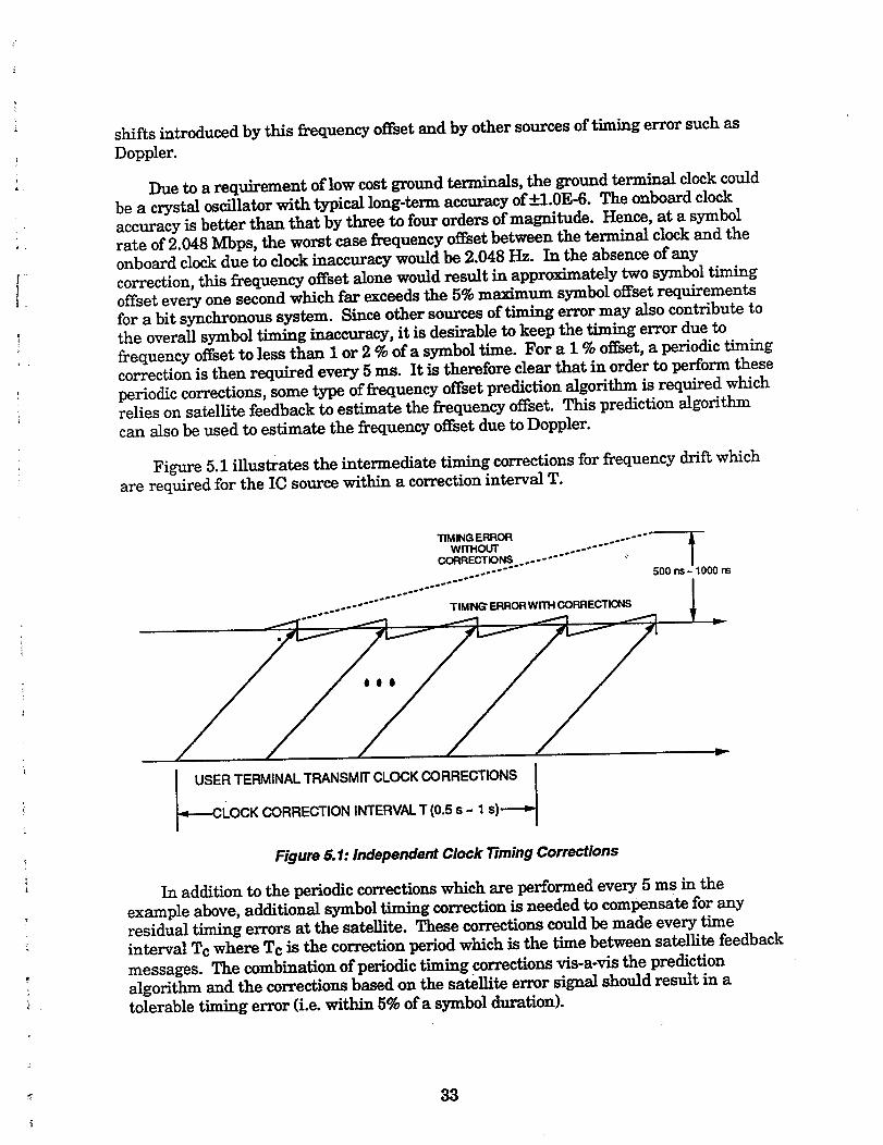
z shifts introduced by this frequency offset and by other sources of timing error such as
Doppler.
Due to a requirement of low cost ground terminals, the ground terminal clock could
be a crystal oscillator with typical long-term accuracy of-+l.0E-6. The onboard clock
accuracy is better than that by three to four orders of magnitude. Hence, at a symbolrate of 2.0481Vlbps, the worst case frequency offset between the terminal clock and the
onboard clock due to clock inaccuracy would be 2.048 Hz. In the absence of any
correction, this frequency offset alone would result in approximately two symbol timingoffset every one second which far exceeds the 5% maximum symbol offset requirements
for a bit synchronous system. Since other sources of timing error may also contribute to
the overall symbol timing inaccuracy, it is desirable to keep the timing error due to
frequency offset to less than 1 or 2 % of a symbol time. For a 1% offset, a periodic timingcorrection is then required every 5 ms. It is therefore clear that in order to perform these
periodic corrections, some type of frequency offset prediction algorithm is required whichrelies on satellite feedback to estimate the frequency offset. This prediction algorithm
can also be used to estimate the frequency offset due to Doppler.
Figure 5.1 illustrates the intermediate timing corrections for frequency drift which
are required for the IC source within a correction interval T.
TIMING ERROR .... "° °_wrrHOUT ......... 1
CORRECTIONS .......... : I
......... 500 _- 1000 m
°o---" ........ TIMP ERR_W_ CORRECTIONS
USER TERMINAL T_NSMff CLOCKCORRECTIONS
_LOCK CORRECTION INTERVALT (0.5 s - 1 s)---P
Figure 5.1: Independent Clock Timing Corrections
In addition to the periodic corrections which are performed every 5 ms in the
example above, additional symbol timing correction is needed to compensate for any
residual timing errors at the satellite. These corrections could be made every timeinterval Tc where Tc is the correction period which is the time between satellite feedback
messages. The combination of periodic timing corrections vis-a-vis the prediction
algorithm and the corrections based on the satellite error signal should result in a
tolerable timing error (i.e. within 5% of a symbol duration).
33

It should be noted here that a small residual timing offset may always be present
due to sources of timing error that are not compensated for by the prediction algorithmand which can not be removed entirely due to the inherent delay in the time the error
measurements are made onboard the satellite to the time the correction is received and
implemented on the ground. However, as long as the timing offset does not exceed a
tolerable value (e.g. 5%), performance should be acceptable.
5.2.1 Independent Clock -Programmable Phase ShiRer (IC-PPS)
Timing corrections to compensate for frequency offset, Doppler, and other sources of
timing error, could be done with a programmable phase shifter which provides a phaseshiftofthe internalclockby a desired amount. This approach isshown in Figure 5.2.
TRANSMITPROCESSOR I v _
I pROGRAMMABLEPHASE SHIFTER I_
CORRECTIONUNIT
.._ RECEIVE
PROCESSOR _
dk
|t
d_t
r='--t
Figure 5.2: Independent Clock with Programmable Phase Shifter (IC-PPS)
A number ofvoltage variablephase shift;devicesare commercially available.Figure
5.3 shows typicalvoltage variable phase shiftercharacteristics.An m-bit quantizer
(digitalto analog converter)can be used to provide programmable controlof the phase
shift.Fine phase adjustments down to a given resolutioncan be achieved by choosing a
large enough value form. However, the inherent nonlinearityin the phase shifter
characteristicsmay introduce deviceinaccuracy errors.Hence, PPS calibrationmay be
necessary.
5.2.2 Independent Clock -Voltage Controlled Oscillator(IC-VCO)
Another approach to implementing timing correctionsat the ground terminal isto
use a voltage controlledoscillatoras a clock source and to implement the timing
correctionsthrough changes to the VCO frequency. This approach isshown in Figure
5.4.
34
L
il
il
iI
i}
i)
]

J
t
m
L
°
"36°° 50
--- j7 .,,,,-, _ m
i
I0
MODULATION VOLTAGE
.__.___.. i
--"'qS
Figure 5.3: Example of Voltage Variable Phase Shifter Characteristics
._ TRANSMIT _ dj__PROCESSOR Clock without
VGO " ,
' i, , Change ,
I CLOCK I _ocrk)Ck_Wnb__
CORRECTION ' :UNIT ,-
I PROCES_)R
_"--t
--[_ '
Figure 5.4: Independent Clock with Voltage Controlled Oscillator (IC-VCO)
Using this approach, long term frequency offsets can be easily compensated for by
setting the VCO control voltage and hence frequency. Also, since phase adjustments aremade continuously, this approach eliminates discrete phase jumps upon correction.
Figure 5.5 shows typical VCO voltage - frequency characteristics. These characteristics
typically exhibit some non-linearity as shown in the figure.
The IC-VCO technique is very sensitive to the linearity of the voltage - frequency
characteristic since phase errors caused by frequency inaccuracy are magnified over the
correction period. High linearity VCOs are available but are more costly. Device
calibration is one option, however this also adds to the cost. Furthermore, aging may
resultin changes in the VCO characteristicswhich may require recalibration.
35

ppm
+600
+500
+400
+300
+200
+100
-100
-200 -
-300 -
-400 -
-500 -
-600 -
EST FOR STRAIGHT LINE
__ ...,o,.,ox/[_ . ---- - OSCILLATOR PERFORMANCE
I I I I l I I - I I I I
-5 -4 -3 -2 -1 0 1 2 3 4 5
Figure 5.5: Example of Voltage Controlled Oscillator Characteristics
5.2.3 Independent Clock - Digitally Controlled Oscillator (IC-DCO)
.?
The digital controlled oscillator (DCO) operates at a higher rate, e.g. 50 times faster,
than the symbol clock. Hence, for a 2.048 MHz symbol clock, the DCO clock rate wouldbe around 100 MI-Iz. The transmit clock is derivgd from the high frequency clock through
the use of a programmable divider. Clock phase adjustments are made by deleting aclock pulse of the high frequency oscillator. The IC-DCO concept is shown in Figure 5.6.
_'1 TRANSMIT
PROCESSOR
I PROGRAMMABLE I_clk _"_DIVIDER
°lCORRECTION
UNIT
I .ECEIVE"il"_" I PROCESSOR I_ --
dk
fllltflflflflflflflflflflflllflflflflflflflflflflflflflflflflflflflflflr
IU_UUUUUUUUUUUUUUUUUUUUU_UUUUUUUUUUUUdW
A
----t
Figure 5.6: Independent Clock with Digitally Controlled Oscillator (IC-DCO)
Obviously, this approach requires a much faster running clock than the other two
approaches. One concern with this approach is the frequency stability of the DCOoscillator which is running at a substantially higher rate than the symbol clock. Also,
36
i.]
]
;LI
i
l
_}
}
J
J
]

timing corrections introduce a discrete albeit very predictable phase jump. The
magnitude of this phase jump (and hence the correction resolution) is directly
proportional to the ratio of the DCO clock to the symbol clock.
5.2.4 Independent Clock - Programmable Delay Line (IC-PDL)
Timing corrections to compensate for frequency offset, Doppler, and other sources of
timing error, could be done using a combination of frame counter and tapped delay line.The flame counter is used to advance or retard the frame timing by an integer number of
symbols. The tapped delay line covers a symbol delay with a sufficiently large number of
delay taps (e.g. 50 for 2% resolution or 20 for 5% resolution). Figure 5.7 shows how this
timing correction is implemented using a programmable delay line.
clk'_ _ _._J L _ |
ol |
clk'
CORRECTION
UNITI RECEIVE
"_-'---] pROCESSORI--
Figure 5.7: Independent Clock with Programmable Delay Line (IC-PDL)
The programmable delay lines typically can provide up to 2 ns resolution with 8 bitcontrol. Hence timing corrections up to 520 ns can be implemented in multiples of 2 ns
using a single PDL. Several PDLs can be cascaded to cover a range equal to one symbol,or lower resolution PDLs (i.e. > 2 us) can be used. For example, for a symbol rate of 1
Msym per second, a PDL with 2 ns resolution will give a timing correction capability of
approximately 0.2 %.
One problem with the PDL approach is that it may produce a superfluous clock pulsewhen a correction is made. If the correction comes after the clock pulse has been delayed
by the initial delay setting but before the new delay setting, the delay line output willconsist of two pulses instead of just one. Because of this problem and other potential
device inaccuracy problems, the PDL approach is not considered further.
5.3 Phase Locked Clock
An alternative to using an independent symbol timing clock at the ground terminal
is to derive the symbol clock from the receive carrier clock. This could be done by a phase
lock loop which tracks the receive signal clock or by a direct clock extraction circuit. In
37
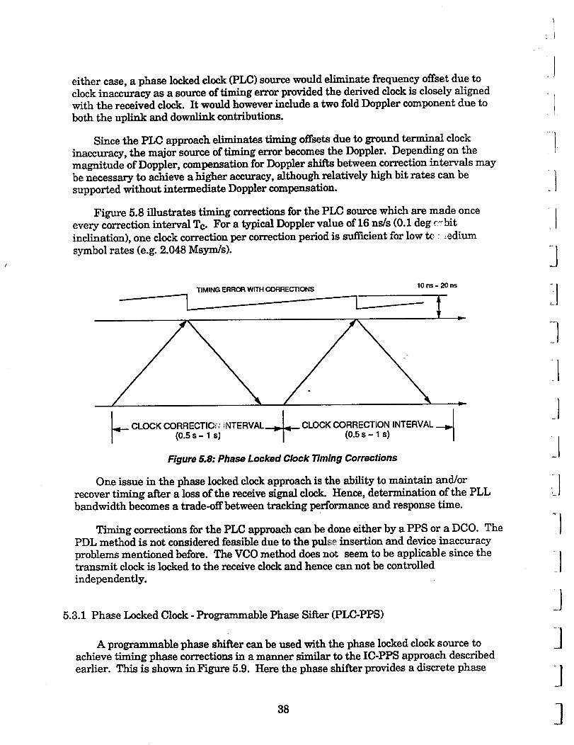
either case,a phase locked clock (PLC) source would eliminate frequency offset due to
clock inaccuracy as a source of timing error provided the derived clock is closely alignedwith the received clock. It would however include a two fold Doppler component due to
both the uplink and downlink contributions.
Since the PLC approach eliminates timing offsets due to ground terminal clock
inaccuracy, the major source of timing error becomes the Doppler. Depending on the
magnitude of Doppler, compensation for Doppler shifts between correction intervals maybe necessary to achieve a higher accuracy, although relatively high bit rates can be
supported without intermediate Doppler compensation.
Figure 5.8 illustrates timing corrections for the PLC source which are made once
every correction interval Tc. For a typical Doppler value of 16 ns/s (0.1 deg _bit
inclination), one clock correction per correction period is suf_cient for low tc :_:edium
symbol rates (e.g. 2.048 Msym/s).
TIMING ERROR WITH CORRECTIONS10 ns - 20 ns
.. CLOCK CORRECTIOi,: iNTERVAL_.___ CLOCKCORRECTION INTERVAL ._(o.ss- 1 sj - I (o.5s- 1s)
Figure 5.8: Phase Locked Clock Timing Corrections
One issue in the phase locked clock approach is the ability to maintain and/or
recover timing after a loss of the receive signal clock. Hence, determination of the PLL
bandwidth becomes a trade-off between tracking performance and response time.
Timing corrections for the PLC approach can be done either by a PPS or a DCO. The
PDL method is not considered feasible due to the pulse insertion and device inaccuracy
problems mentioned before. The VCO method does not seem to be applicable since thetransmit clock is locked to the receive clock and hence can not be controlled
independently.
5.3.1 Phase Locked Clock - Programmable Phase Sifter (PLC-PPS)
A programmable phase shiftercan be used with the phase locked clock source to
achieve timing phase correctionsin a manner similarto the IC-PPS approach described
earlier.This is shown in Figure 5.9. Here the phase shiRer provides a discretephase
38
I
]
]
]
]
1
]
]
]
]
]

£.
adjustment to the transmit clock, which in turn is locked to or derived from the receive
clock.
_____ TRANSMIT
PROCESSOR
+IP_se SHIF"rER,,I-- I
,,1I CLOCK ]I CORRECTION I "r
I u.rr it
RECEIVEPROCESSOR
dk
I
c11¢ i/
+ -"i,,I"- _ _o_,.
Figure 5.9: Phase-Locked Clock with Programmable Phase Shifter (PLC-PPS)
5.2.2 Digitally Controlled Oscillator (DCO)
Figure 5.10 shows an alternative to PLC timing phase corrections using a DCO. Asin the IC-DCO approach described earlier, timing phase corrections are implemented by
controlling the number of DCO clock cycles within a transmit clock cycle.
._ TRANSMITPROCESSOR r _
clk'l
I nl l'4_1[_Loo+:o:+l
"_'-'--'i RECEIVEPROCESSOR I--
dk
flfltflTMflflflflflflflflrlilfliMIlflflililflflflflflTlflllflflflill _t
IU_UUUUUUUUUUUUUUUtlUUIIUUUUIIUUUUUUUUUII
nclocks , nclocks , n'clocks t ,n' clocks
Figure 5.10: Phase-Locked Clock with Digitally Controlled Oscillator (PLC-DCO)
5.4 Open Loop Synchronization (OLS)
Open loop synchronization (OLS) whichis shown in figure 5.11 is performed by
deriving clock corrections from precision ranging of the satellite location to compensatefor satellite motion. Technically, OLS does not require onboard phase error
measurement. However, in practice it might be necessary to monitor abnormal timing
39

error causedbyground terminal malfunctionor other sourcesof timing error. Thus, thistechniqueis not attractive for actual implementation.
,_1 TRANSMIT
PROCESSOR
I u.rr I I
Satellite 4 F dk IPosa onData/ I FRECEIVE
PROCESSOR _
Figure 5.11: Clock Correction Based on Open Loop Synchronization
Since OLS can only compensate for the Doppler component in timing errors, the
transmit clock must be derived from a phase-locked clock source to eliminate timing
errors due to clock frequency offsets.
The limitation of the OLS approach lies in the ranging accuracy _quired at
moderate bit rates. For example, a _+10 m range error, which is not uncommon in a
practical ranging system, results in +33 ns phase error. Other errors include delaycalibration errors (both RF and baseband) of use_ terminals and onboard equipment,
range prediction uncertainty, and implementation errors. These error terms would limitthe supportable bit rate to no more than 500 KbitYs. Because of the low supportable bitrates and the lack of onboard monitoring of the ground terminal transmit timing, this
option is not recommended.
4O
--'L
.... i
B
I

4._
]
Section 6
Timing AccuracyThis section presents an overview description of acquisition and synchronization
procedure, analytical models for timing analysis, numerical values for expected timingerrors and computer simulation results. A general conclusion is also made for the
maximum supportable bit rate in a bit synchronous system.
6.1 Acquisition and Synchronization Overview
Acquisition and synchronization of system timing in a bit synchronous system is
performed through specialized acquisition and synchronization time slots. As aminimum, a single time slot on an LR-TDMA carrier may be used for both acquisition
and synchronization by all the users in the system when the number of users is small.
However, for a moderate to large number of users, several such time slots may be
required, with some slots designated for acquisition and others for synchronization.
In a bit synchronous system, the purpose of acquisition is to achieve rough
alignment of user terminal timing with the onboard timing in order to be able to starttransmitting TDMA data bursts from the user terminal. An acquiring user terminal
starts out by monitoring the downlink transmission from the onboard processor and
deriving its timing from the downlink frame timing. Satellite range information mayalso be broadcast on the downlink to aid in initi_ acquisition. Based on the downlink
frame timing, the terminal transmits an acquisition burst in a specified acquisition slot.
The acquisition burst identifies the terminal and contains a preset data pattern that is
used by a special acquisition/synchronization processor onboard the satellite to determinethe burst timing offset in relation to the onboard reference timing. A correction message
is then sent back to the acquiring terminal requesting a timing correction which mayinclude an offset of several symbols plus a fraction of a symbol. The user terminal then
proceeds to correct its timing and retransmits another acquisition burst which is again
processed in the same manner onboard the satellite. This procedure is repeated ifnecessary until the user terminal timing in within a specified tolerance from the onboard
timing (e.g. 10% of a symbol time), in which case the user terminal can begintransmitting its data bursts in their allocated time slots on one or several LR-TDMA
carriers.
Once acquisition has been established and the user terminal is now transmitting its
data bursts, a synchronization procedure is necessary to keep the ground terminal timing
within the specified tolerance from the onboard timing. This is done through periodic
timing error measurements onboard the satellite. User terminals which have already
acquired system timing will periodically transmit a synchronization burst consisting of a
predetermined pattern which allows measurement of the timing phase error onboard thesatellite. The timing phase error is relayed back to the user terminal which implements
timing error correction based on the received feedback from the onboard processor.
Timing error correction may be accomplished in several ways, which are discussed in
detail in the following sections.
41
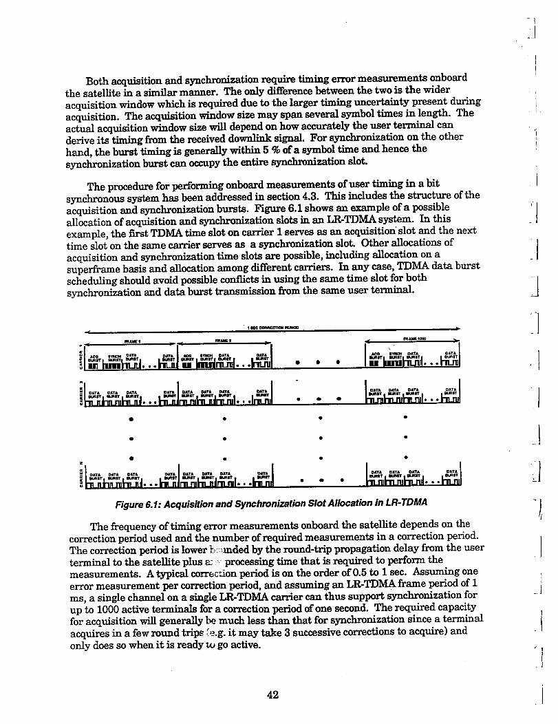
-I
Both acquisitionand synchronization require timing error measurements onboard
the satellitein a similarmanner. The only differencebetween the two isthe wider
acquisitionwindow which isrequired due to the largertiming uncertainty present during
acquisition.The acquisitionwindow sizemay span several symbol times in length. The
actualacquisitionwindow sizewilldepend on how accurately the user terminal can
deriveitstiming from the received downlink signal.For synchronization on the other
hand, the burst timing isgenerallywithin 5 % ofa symbol time and hence the
synchronization burst can occupy the entiresynchronization slot.
The procedure for performing onboard measurements ofuser timing in a bit
synchronous system has been addressed in section4.3. This includes the structureofthe
acquisitionand synchronization bursts. Figure 6.1 shows an example ofa possible
allocationofacquisitionand synchronization slotsin an LR-TDMA system. In this
example, the firstTDMA time sloton carrierI serves as an acquisitionslotand the nexttime sloton the same carrierserves as a synchronization slot.Other allocationsof
acquisitionand synchronization time slotsare possible,including allocationon a
superframe basis and allocationamong differentcarriers.In any case,TDMA data burst
scheduling should avoid possibleconflictsin using the same time slotfor both
synchronization and data burst transmission from the same user terminal.
1 _C CORRECTt_d PERt_O
• • @
DATA
• 4) 4)
DUiqST mutqlJT iuqlrr
O • • •
,: n]... rlu'U nlrn.rd •. • rll_n] * * '''
Figure 6.1: Acquisition and Synchronization Slot Allocation in LR-TDMA
The frequency oftiming error measurements onboard the satellitedepends on the
correctionperiod used and the number ofrequired measurements in a correctionperiod.
The correctionperiod islower _,:_mded by the round-trippropagation delay from the user
terminal to the satelliteplus _ _:-processing time that isrequired to perform the
measurements. A typicalcorrectionperiod ison the order of 0.5 to I sec. Assuming one
error measurement per correctionperiod,and assuming an LR-TDMA frame period of1
ms, a singlechannel on a singleLR-TDMA carriercan thus support synchronization for
up to 1000 activeterminals fora correctionperiod ofone second. The required capacity
for acquisitionwillgenerallybe much lessthan that for synchronization since a terminal
acquires in a few round trips:e.g.itmay take 3 successivecorrectionsto acquire) and
only does so when itisready to go active.
42
if
il
L
J
!
Il
I
I
*I
I
i
A possible concern in synchronization for an LR-TDMA system is that the databursts may be transmitted on carriers which are different from the carrier over which the
synchronization channel and consequently the timing error measurements are made.
This may introduce a frequency dependent timing error. However, by examining thesource of this timing errors, it becomes clear that this effect is negligible. The main
sources of frequency dependent timing errors are filtering, HPA, and possible differences
in delay through differentonboard demodulators. Digitalfilteringisemployed at the
user terminal and equalizationas well as operation away from the edges ofthe
transponders may reduce the effectofgroup delay. HPA characteristicsare usually wide
baud enough not to introduce any frequency dependent time delays within the range of
interest.Finally,ifa shared demodulator isused on allcarriersthen there isno problem
in terms ofdifferentdelay values,as willprobably be the case in an LR-TDMA system.
However, ifindividualdemodulators are used, care must be taken tomatch the delays
through these demodulators to within a tolerablelimit.However, in the unlikelyevent
that significantfixedfrequency dependent delay differencesare present, delay
compensation may be implemented at the user terminal as a function ofthe transmit
carrierfrequency.
6.2 Timing Error Analysis
Timing analysis has been performed for the clock correction techniques described in
the previous section. This section first describes a general clock control model and then
presents specific models for the independent clock (IC) and phase locked clock (PLC)clock correction techniques. Each model analyzed includes numerical values to assess
the feasibility of a bit synchronous system, identification of critical parameters, andillustrations of clock correction performance obtained from simulation.
6.2.1 General Model
A general clockcontrolmodel isshown in Figure 6.2. The timing error of a TDMA
burst ismeasured on the satelliteby comparing the phase ofthe received clock against
that ofthe onboard master clock,is.The measured phase error,denoted by "y"in the
figure,issent to the user terminal over a downlink signalingchannel. The user terminal
performs correction,w, on itstransmit clock,fu,in such a manner that TDMA bursts
transmitted afterthe correctionarriveat the satellitewithin a small fractionofa symbol
periodrelativeto the expected onboard timing. The heart ofthissystem isa mechanism
ofperforming clock correction.
The IC model includes only the uplink Doppler component, Pd, while the PLC model
must consider both the downlink and uplink Doppler components. The controlloop
(satellite-user terminal -satellite)contains various error terms, in addition to the
onboard phase measurement error.Also,the loop must be stablesuch that the phase
error does not increase without a bound.
43

SATELLITE
Pd
I .u.sT LI
USER TERMINAL
Figure 6.2: General Clock Control Model for Bit Synchronous System
6.2.2 Independent Clock (IC) Control Technique
The major issue associated with the IC control technique is the amount of drift of auser terminal clock, which must be compensated to assimilate with that of the onboard
clock and Doppler shifL A typical low-cost crystal oscillator has an aging characteristic
of about one part per 108 to 109 over 24 hours. With several months0f operation, the
clock accuracy will be reduced to 1 x 10⁶ to 1 x 10⁷, producing a 1 lm to 100 ns of phaseshift over one second The clock control circuit mast properly compensate for this large
drift based on measured phase errors. Another factor which must also be taken into
account in designing the IC system is the predictability of drift. Although long-term drift
over several months can be fairly well characterized, its short-term component often
exhibits a peculiar behavior, such as a sudden jump in the drift rate and changing its
direction (positive to negative or negative to positive). Because of these reasons, the
proposed control algorithm employs a robust technique, which has been considered
previously for controlling an onboard clock in satellite-switched TDMA (SS-TDMA) and
onboard processing systems.
The timing correction procedure for the independent clock is shown in Figure 6.3. To
prevent a large phase jump due to a single clock correction, corrections are made in small
steps during a correction period. The correction value is derived from the onboard errormeasurements which are performed once per correction period and transmitted down to
the user terminal. A prediction algorithm is used at the ground terminal to predict theclock drift based on the received onboard error measurements, and to consequently
determine the value of the intermediate corrections to ensure close tracking of the
onboard timing.
44
il
J
//I
i

ERROR ERRORMEASUREMENT MEASUREMENT
i_._____CLOCK CORRECTION INTERVAL+ CLOCK CORRECTION INTERVAL--_(o.ss - 1s) (o.ss - 1s)
START OF STARTOF STARTOFCORRECTION CORRECTION CORRECTION
PERIOD PERIOD PERIOD
Figure 6.3: Timing Correction Procedure for IC
6.2.2.1 IC Timing Analysis
The IC clock correction technique is based on references [14-16]. The phase error at
the end of the nth correction interval is
Yn = Yn-1 + Sn
where Sn is the phase error in the current correction period and is given by
ta
sn =ta-1
where p=(t), pd(t), and p,(t) are normalized user terminal clock drift, Doppler shift and
satellite clock drift, respectively. The term Wn represents a normalized clock correctionvalue for the current correction period. Integration in the above equation is over a clock
correction period Tc (=tn - tn-1).
The drift and Doppler terms can be expressed in the following forms:
where
p.(t) = p.ot+ Ap.(t)
pa(t)= paoSin(-_--a )
p.(t)= p,ot+ Ap,(t)
P.o user terminal clock aging
45
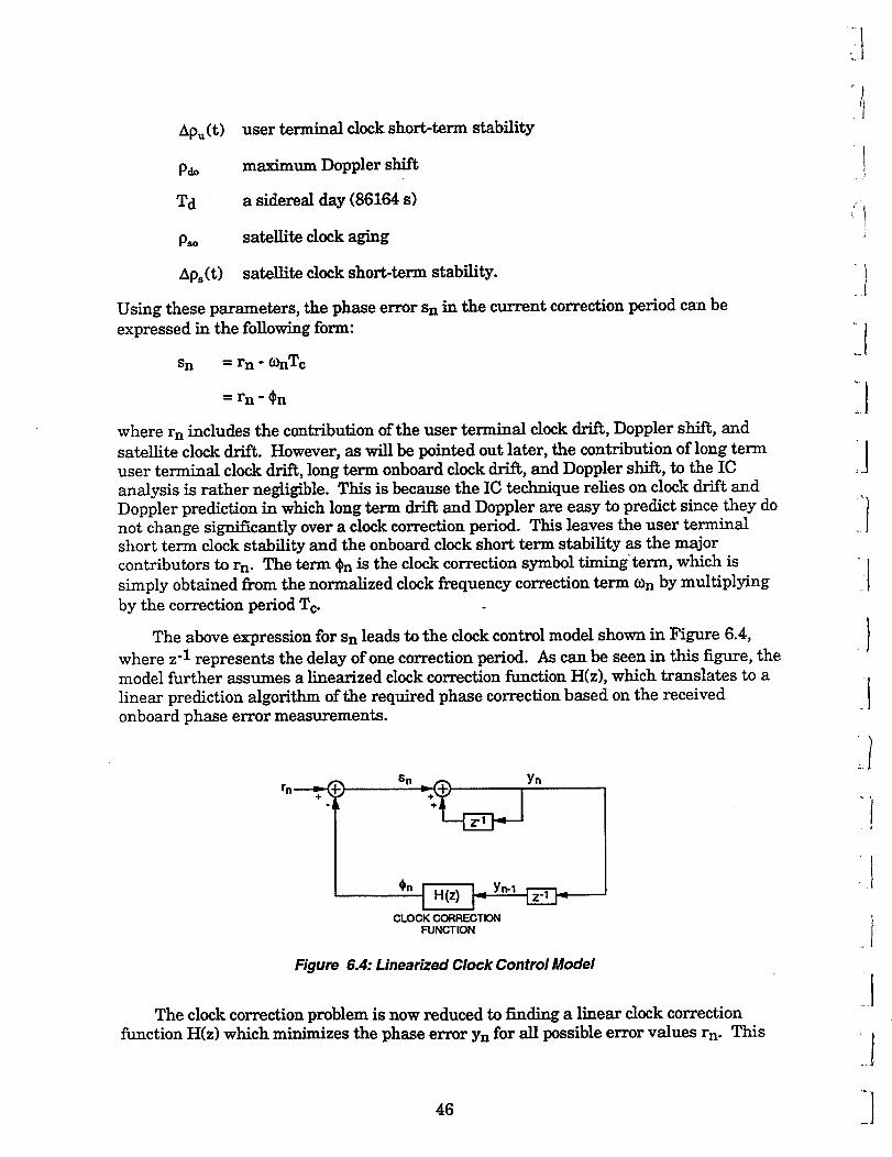
Apu(t) user terminal clock short-term stability
Pdo
Td
maximum Doppler shift
a sidereal day (86164 s)
p_o satellite clock aging
Aps(t) satellite clock short-term stability.
Using these parameters, the phase error Sn in the current correction period can be
expressed in the following form:
Sn = rn -a_nTc
= rn -_n
where rn includes the contributionofthe user terminal clockdrift,Doppler shift,and
satelliteclock drift.However, as willbe pointed out later,the contributionof long term
user terminal clock drift,long term onboard clockdrift,and Doppler shift,to the IC
analysis israther negligible.This isbecause the IC technique relieson clock driftand
Doppler prediction in which long term _ and Doppler are easy to predict since they do
not change significantly over a clock correction period. This leaves the user terminalshort term clock stability and the onboard clock short term stability as the major
contributors to rn. The term _n is the clock correction symbol timingterm, which is
simply obtained from the normalized clock frequency correction term O_n by multiplying
by the correction period Tc.
The above expression for Sn leads to the clock control model shown in Figure 6.4,
where z-1 represents the delay of one correction period. As can be seen in this figure, themodel further assumes a linearized clock correction function H(z), which translates to a
linear prediction algorithm of the required phase correction based on the received
onboard phase error measurements.
rn÷
SR
0nCLOCK CORRECTION
FUNCTION
Figure 6.4: Linearized Clock Control Model
The clock correction problem is now reduced to f'mding a linear clock correction
function H(z) which minimizes the phase error Yn for all possible error values rn. This
46
rt
!
i
i/

!
problem has been extensively analyzed in the past for onboard clock control in SS-TDMAand onboard processing systems [14-16]. The optimum function, according to [14], is
given by
H(z)- 2 - z"1 1I z"1= i+_. l_z -1"
The clockcorrectionfunction H(z) isessentiallycomposed ofan accumulator (i.e.a
firstorder errorpredictor)and a constant (i.e.a 0th order predictor).The accumulator
function resultsin long term corrections which remove the effectsoflong term driftand
Doppler, while the 0th order predictionterm attempts to compensate forshort term
errors.
Figure 6.4 now can be redrawn as Figure 6.5. This figure also includes the error
components produced by the satellite, esn, and the user terminal, elm. These termsaccount for error contributions from such factors as device inaccuracies, quantization,
logic jitters, and measurement inaccuracies. A breakdown of the error components andtheir statistical characteristics are given later in this section.
esn
H(z): OPTIMAL CORRECTIONCIRCUIT
Figure 6.5: Optimal Clock Control Model with Various Timing Error Sources
From Figure 6.5, the z-transform of the measured error Yn is obtained as follows:
Y(z) = (I -z'I)[R(z)-Eu(z)] - z'l(2" z'I)Es(z)
where R(z),Eu(z) and Es(z) are respectivelythe z-transforms ofrn, eun, and esn. The
discretetime domain expression forY(z) isgiven by
yn = rn -rn-1"eun + eun-1 -2esn-1+ esn-2
The errorterms shown in Figure 6.5 are further divided intovarious error
components. Table 6.1 liststhese error components and theirstatisticalcharacteristics.
47
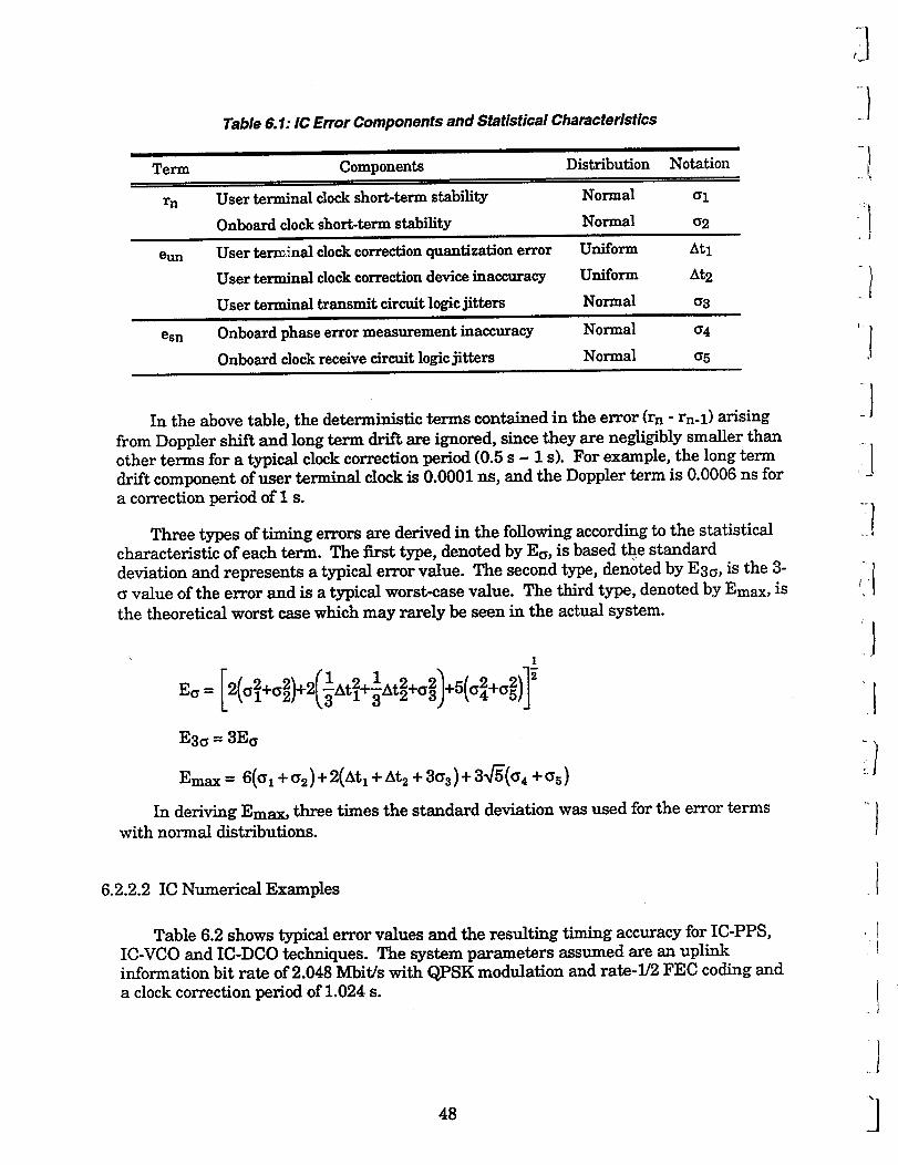
Tern
rn
Table 6.1: IC Error Components and Statistical Characteristics
Components
User terminal clock short-term stability
Onboard clock short_term stability
Distribution Notation
Normal al
Normal 02
J
eun User tervcinal clock correction quantization error
User terminal clock correction device inaccuracy
User terminal transmit circuit logic jitters
Uniform At1
Uniform At2
Normal a3
esn Onboard phase errormeasurement inaccuracy
Onboard clockreceivecircuitlogicjitters
Normal a4
Normal a5
In the above table,the deterministicterms contained in the error (rn -m-l) arising
from Doppler shiftand long term driftare ignored, sincethey are negligiblysmaller than
other terms for a typicalclock correctionperiod (0.5s ~ I s).For example, the long term
driftcomponent ofuser terminal clockis0.0001 ns, and the Doppler term is0.0006 ns for
a correctionperiod of I s.
Three types of timing errors are derived in the following according to the statisticalcharacteristic of each term. The first type, denoted by Ea, is based the standard
deviation and represents a typical error value. The second type, denoted by E3o, is the 3-
value of the error and is a typical worst-case value. The third type, denoted by Emax, is
the theoretical worst case which may rarely be seen in the actual system.
\ 1
E_= [ ( i _ (332c_2+<_22 2 1At2+1At22+G 21+5(G42+G2) 2]
E3v = 3Eo
Emax= 6(_i +a2)+ 2(At1 + At2 + 8c3) + 3_f5(<_4 +cs)
In deriving Emax, three times the standard deviation was used for the error terms
with normal distributions.
iI
6.2.2.2 IC Numerical Examples
Table 6.2 shows typical error values and the resulting timing accuracy for IC-PPS,
IC-VCO and IC-DCO techniques. The system parameters assumed are an uplink
information bit rate of 2.048 Mbit/s with QPSK modulation and rate-l]2 FEC coding and
a clock correction period of 1.024 s.
48

Table 6.2: Typical Timing Error Parameter values and Estimated Phase Errorsfor PLC-PPS, PLC-VCO and PLC-DCO Techniques
Term Notation Typical Value IC-PPS IC-VCO IC-DCO
rn al 0.3 ns 0.3 ns 0.3 ns 0.3 ns
G2 ~ 0 0 ns 0 ns 0 ns
eunAtl see explanation below 2.7 ns 2.5 ns 5 ns
At2 see explanation below 1.4 ns 2 ns 0 ns
a3 1 ns 1 ns 1 ns 1 ns
esn a4 Ts/100 4.9 ns 4.9 ns 4.9 ns
a5 1 ns 1 ns 1 ns 1 ns
E_ 11.5 ns 11.5 ns 12.0 ns
E3_ 34.5 ns 34.6 ns 35.9 ns
Emax 55.5 ns 56.3 ns 57.3 ns
The numerical values in the above table are typical values which are based on
manufacturers specification and/or implementation details. The user terminal short
term stability (al) of 3x10 -10 (0.3 ns over 1.024 sac correction period)sis typical for a low
cost VCXO, while the onboard clock short term stability (G2) is typically two to three
orders of magnitude better and hence is negligible in comparison.
User terminal clock correction quantization error (Atl) is assumed to be +_2 degrees
for the PPS which is typical with 8-bit control of phase shift. This translates to 2.7 ns at
a symbol rate of 2.048 Msps. For the VCO, a _+10-5 worst case normalized frequency
accuracy (typical) and 12-bit control over that accuracy range results in a quantizationerror of 2.5 ns over the 1.042 s correction period. The DCO user terminal clock correction
error (At1) is based on a 100 MHz clock which is divided down to the 2.048 MHz symbol
clock. Hence, a pulse deletion at 100 MHz results in a 10 ns phase step so that the
quantization error from the desired clock phase will be at most half that value or 5 ns.
User terminal clock correction device inaccuracy (At2) is a direct result of the
nonlinearity and variations in characteristics among the clock correction devices which
may even become more apparent with aging. For example, the VCO transfercharacteristics exhibit a certain nonlinearity (see Figure 5.5) which may require initial
calibration for precise frequency control. However, even with initial calibration, these
characteristics may shii% which would require additional compensation. If the change incharacteristics is simply a linear translation (i.e. the actual shape does not change),
compensation will be easier to implement. However, if the transfer characteristic also
changes with aging, recalibration may become necessary. Hence it becomes clear that ina low cost implementation, precise frequency (or phase) control is impractical and certainallocation must be made for errors introduced by device inaccuracies. In the PPS case, a
1-deg additional error is assumed based on typical PPS characteristics which translates
to 1.4 ns at a symbol rate of 2.048 Msps. For the VCO case, a 2-ns error is derived by
assuming a worst case inaccuracy of 10% in the VCO characteristics,and a worst case
49

correction of 20 ns over a correction period (approx. 4% of a symbol period). The DCO
technique, by virtue of digital pulse deletion control, does not suffer from device
inaccuracy errors.
User terminal transmit circuit logic jitters (as) and onboard clock receive circuit logic
jitters (_5) are assumed to be 1 ns which is typical for CMOS/TrL technology. Onboardphase error measurement inaccuracy (_4) is assumed to be 1% of a symbol period asdiscussed in section 4.3.
6.2.2.4 IC Simulation Results
Computer simulation of the three IC control techniques was performed with the
same parameters used in the IC timing analysis numerical examples above. Table 6.3
provides a summary of the IC simulation parameters.
Table 6.3: Independent Clock Simulation Parameters
Information Bit Rate 2.048 Mbit/s
Modulation QPSK with R-l/2 FEC Coding
Symbol Period (Ts) 488 ns .
Clock Correction Interval 1.024 s
Onboard Measurement Error Ts/100
Doppler Shii_ 8 x 10 .9 (On_ _ :_y Satellite to Earth)
Terminal Clock Drift I x 10 .7
Satellite Clock Drii_ 1 x 10 .9
DCO Frequency 100 MHz
Simulation results for IC-PPS technique are given in Figure 6.6. The simulation run
was performed over 40 seconds and showed the phase error performance to be in
agreement with the analysis results. All recorded values fall within the E3G range of
_+34.5 ns as predicted in the _nalysis. This performance however may be inadequate for a
bit synchronous system if the phase error values were limited to fall within -+5% of a
symbol period (+_24.4 ns at 2.048 Msps). However, ifa wider range of phase error (and
consequently higher degradation in SNR) is tolerable, the IC-PPS performance may be
adequate.
Figure 6.7 shows the simulation results for the IC-VCO technique over a 40 ssimulation run. Here again the simulation results are within close agreement with the
analysis results which predict an Esa of 34.6 ns. As can be seen from this figure, the
simulation values all fall within the expected range. However, as in the case of the IC-
PPS technique, the performance is still short of the desirable timing error of 5% of a
symbol period (+_24.4 ns at 2.048 Msps).
5O
il
i!
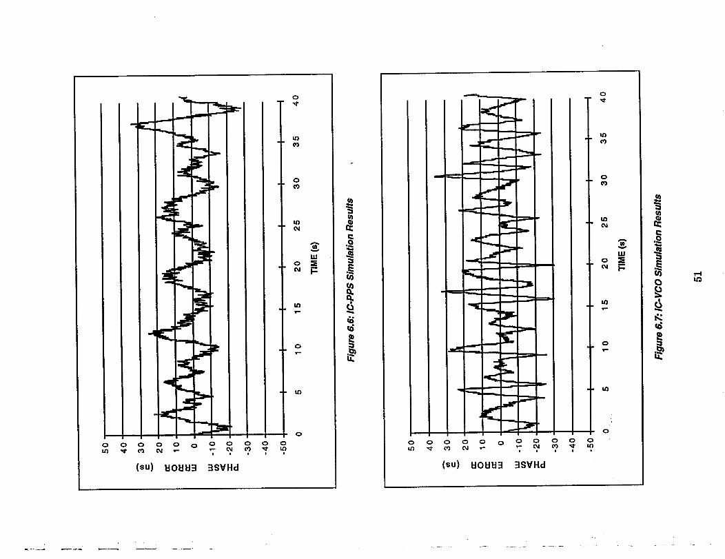
ml=m P
P
r
'Ip'
_I¢,.
am=,
i
0 0 0 0 0 0 0 0 0 0 0
(su) 1:101:11:1:1=ISVHd
o
to
o
_9
o;mz31P-
ov--
It)
0
¢:
41 ..,,
_rP
d,,¢.,,.w-,-,w,=
-.---j m
C"
,,¢;.._.
"" "--" i
i_-.==
B,
0 0 0 0 0 0 0 0 0 0 0
(su) I:IOHI:I3 3SVHd
o• , q_.
i,o= ,
co
.o
u_
ole-
o
0
=1
LP_

Finally, Figure 6.8 shows the simulation results for the IC-DCO technique. Here toothe simulation results seem to support the analytical value derived earlier in that all
except one simulation value fall within the E3o range predicted by the analysis. As in
the case of the IC-PPS and IC-DCO techniques, the worst case timing error exceeds _+5%
of the symbol period.
i!
50
40
_'= 3o]"_" I
20
= i=0 1(1
w 0
-20
=- II-30
-40
-50
t I1 r i Illr i rl i I
I I
5 10
I I I I I I
15 20 " 25 30 35 40
TIME (s)
i]
I_i
Figure 6.8: IC-DCO Simulation Re'suits
6.2.2.5 Stability Problem
The previous analysis of the IC control techniques has demonstrated their
inadequacy in meeting bit synchronous timing requirements at least with the
representative parameters used in the simulation. The IC techniques also exhibit
unstable operation under certain conditions. This is primarily due to the time lag
between onboard phase error measurement and user terminal clock correction. Clock
drift prediction is performed based on the phase error measurement made about 175 msearlier (125-ms propagation delay and 50-ms processing time) and exhibits unstable
operation for a short correction interval [15]. Figure 6.9 illustrates the instabilityproblem in a simulation run using the IC-PPS technique with a shorter correction periodof 512 ms and a terminal clock drif_ of 1.0E-6. The instability problem may be avoided by
selecting a long correction period, such as 1.024 s or longer.
52
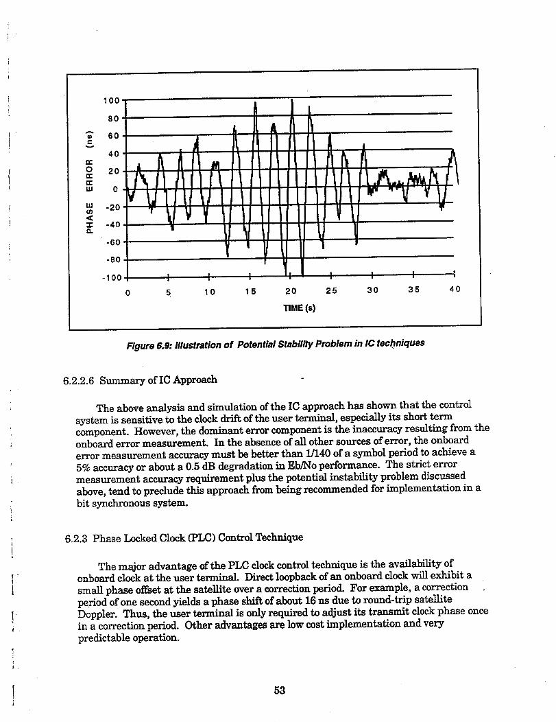
lOO
-80
-lOO
o
I I I I i
5 1 o 15 20 25 30 35
TIME (s)
I
4o
Figure 6.9: Illustration of Potential Stability Problem in IC techniques
t
6.2.2.6 Summary of IC Approach
The above analysis and simulation of the IC approach has shown that the control
system is sensitive to the clock drift of the user terminal, especially its short term
component. However, the dominant error component is the inaccuracy resulting from theonboard error measurement. In the absence of all other sources of error, the onboard
error measurement accuracy must be better than 1/140 of a symbol period to achieve a
5% accuracy or about a 0.5 dB degradation in Eb/No performance. The strict errormeasurement accuracy requirement plus the potential instability problem discussed
above, tend to preclude this approach from being recommended for implementation in a
bit synchronous system.
6.2.3 Phase Locked Clock (PLC) Control Technique
The major advantage of the PLC clock control technique is the availability ofonboard clock at the user terminal. Direct loopback of an onboard clock will exhibit a
small phase offset at the satellite over a correction period. For example, a correction
pe_od of one second yields a phase shift of about 16 ns due to round-trip satellite
Doppler. Thus, the user terminal is only required to adjust its transmit clock phase once
in a correction period. Other advantages are low cost implementation and very
predictable operation.
53

The timing correctionprocedurefor the phase-lockedclockis shownin Figure 6.10.Here,only oneuser terminal clockcorrectionis madeduring a correction period. Thevalue of the correction is derived directly from the onboard error measurement which is
performed once per correction period and transmitted down to the user terminal.
ERROR ERRORMEASU REM ENT M EASUREM ENT
.__ CLOCK CORRECTION INTERVAL._ CLOCK CORRECTION INTERVAL_._(0.5 s ~ 1 s) (0.5 s - 1 s)
START OF START OFCORRECTION CORRECTION
PERIOD PERIOD
START OFCORRECTION
PERIOD
Figure 6.10: Timing Correction Procedure for PLC ,*
The following subsections present the phased locked clock control model and derive
expressions for timing accuracy. Timing errors are plotted as a function of TDMA bitrate and onbeard timing measurement inaccuracy. Simulation results are also provided
to verify analytical results.
6.2.3.1 PLC Timing Analysis
An analytical model for PLC timing control is shown in Figure 6.11. The onboard
clock, is, generates a downlink signal with an injected timing error of est. The signal will
incur a nominal one-way propagation delay of TD and an additional delay, edd, due to
satellite motion. The user terminal introduces an error, eur, in the process of
demodulation and generation of a phase-locked terminal clock. This clock is adjusted by
the amount of phase error measured at the satellite. The user terminal further adds a
transmit error term eut in the process of generating and transmitting the TDMA bursts.
The transmitted signal will be delayed by the amount of the nominal propagation delay,
TD, and uplink Doppler, edu. The signal received at the satellite will experience various
measurement errors, esr, caused by clock jitters, sampling quantization, non-ideal phase
estimation and data quantization prior to the transmission of measured phase error.
54
ilI
.I
J
.)
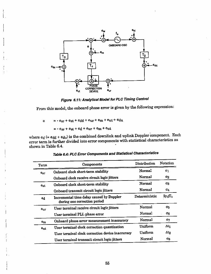
Eedu
.I-
+
v
e_ estfs +
ONBOARD OSG
+ 1
E
eut DEVICE eur
-_--edd
Figure 6.11: Analytical Model for PL C Timing Control
From this model, the onboard phase error is given by the following expression:
e = - esr + est + edd + eur + em+ eut + edu
= - esr + est + ed + eur +em + eut
where ed (= edd + edu) is the combined downlink and up]ink Doppler component. Each
error term is further divided into error components with statistical characteristics as
shown in Table 6.4.
Table 6.4: PLC Error Components and Statistical Characteristics
Term Components
esr Onboard clock short-term stability Normal al
Onboard clock receive circuit logic jitters Normal c2
est Onboard clock short-term stability Normal 03
Onboard transmit circuit logic jitters Normal o4
ed Incremental time delay caused by Doppler Deterministic 2pdTcduring one correction period
eur User terminal receive circuit logic jitters Normal o5
User terminal PLL phase error Normal o6
em Onboard phase errormeasurement inaccuracy Normal o7
eut User terminalclockcorrectionquantization Uniform At1
User terminal clock correction device inaccuracy Uniform At2
User terminal transmit circuit logic jitters Normal o8
Distribution Notation
55

In the above table,symbols Pd and Tc denote one-way Doppler shiR (i.e.,8 x 10-9for 0.1°
inclination)and the clock correctionperiod,respectively.
Three types oftiming errorsare derived in the followingaccording to the statistical
characteristicof each term. The firsttype,denoted by E_, isbased the standard
deviation and represents a typicalerrorvalue. The second type,denoted by E3c, isthe 3-
o value ofthe error and isa typicalworst-case value. The thirdtype,denoted by Emax, is
the theoreticalworst case which may rarelybe seen in the actualsystem.
1
+2p<,zo
1
1 9_
8
E_ = 3_:_, + A_ +At 2+2p,_Tcn=l
As in the IC error analysis,E_ assumes a worst-case errorvalue of3a foran error term
with normal distribution.
The above equations are evaluated fortypicalsystem parameters in the following
subsection.
6.2.3.2 PLC Numerical Examples
Typical system parameters forvarious timing error components are shown in Table
6.5 along with numerical examples forthe PLC-PPS and PLC-DCO techniques.
The values given in the above table are based on the following assumptions. The
phase measurement error, ¢_7, is assumed to be one hundredth of a symbol period and 4.9ns for the information rate of 2.048 Mbit/s with rate-l/2 coding and QPSK modulation.
This is equivalent to a typical worst-case value to 14.7 ns (3a value). The Doppler term
assumes a station keeping accuracy of_+0.1 ° in inclination and drift which yields about 8
ns/s of phase error. The clock correction cycle is 512 ms. The DCO output frequency is
100 MHz, corresponding to a basic correction inaccuracy of 5 ns. The PPS clock
correction quantization accuracy of 0.1 ns is based on 12-bit quantization over a symbol
period. PPS clock correction device inaccuracy is based on an assumption of i degree
uncertainty in the voltage-phase transfer curve..
The typical worst-case phase errors, E3¢_, are 25.5 ns and 26.5 ns for PPS and DCO.
These values correspond to 5.2 percent and 5.4 percent of a symbol period. This example
illustrates that implementation of a bit synchronous system at 2.048 Mbit/s is feasible.
56
Jl
iii
i-I
i
JJ
J..l
I
_l
71
7J

t ..
i
I
ix.
Table 6.5: Typical Timing Error Parameter Values and Estimated Phase Errorsfor the PLC-PPS and PLC-DCO Techniques
Term Notation Typical Value PLC-PPS PLC-DCO
esr Ol ~ 0 0 ns 0 ns
o2 i ns I ns I ns
est o3 ~ 0 0 ns O ns
O4 I ns 1 ns 1 ns
ed 2pdTc 2pdTc 8.2 ns 8.2 ns
eur 05 1 ns 1 ns 1 ns
c6 i ns i ns 1 ns
em o7 Ts/100 4.9 ns 4.9 ns
eut At1 see explanation below 0.1 ns 5 ns
At2 see explanation below 1.4 ns N/A
07 1 ns 1 ns 1 ns
Eo 13.6 ns 14.3 ns
E3_ 25.5 ns 26.5 ns
Emax 39.3 ns _42.9 ns
Among the error components given in the above table,three terms are dominant: the
phase measurement error,Doppler component and DCO correctionresolution.The
phase measurement error can be reduced significantlyby an averaging technique,
although thiswillconsume some transponder capacity. The potentialimprovement
factorwith averaging willbe described in a latersection.The Doppler error term given
in the table isa worst-case value and occurs only when the inclinationapproaches the
stationkeeping maximum. This error term can be reduced with betterstationkeeping
and alsowith a Doppler predictiontechnique which willbe described later.The DCO
error component can be made smaller with the use of a higher frequency oscillator.
However a higher frequency oscillatorwilladd circuitcomplexity in the form ofhigh-
speed logicand a largerprogrammable divider.
6.2.3.3 PLC Parametric Analysis
Figures 6.12 and 6.13 illustrate the effect of the onboard phase measurement erroron the overall phase error when supporting different bit rates ranging from 100 kbit/s to
10 Mbit/s. Figure 6.12 applies to the PLC-PPS technique while Figure 6.13 shows the
parametric results for the PLC-DCO technique.
57

(O011::13d "IOBi_IAS ..-I0
oo
_
1
measurement accuracy results in a significantly lower supportable bit rate for the same
phase error criterion.
6.2.3.4 PLC Simulation Results
Computer simulation of the two PLC control techniques was performed with thesame parameters used in the PLC timing analysis numerical examples above. Table 6.6
provides a summary of the PLC simulation parameters.
Table 6.6: Phase-Locked Clock Simulation Parameters
Information Bit Rate
Modulation
Symbol Period(Ts)
Clock CorrectionInterval
Onboard Measurement Error
Doppler Shift
SatelliteClock Dri_
DCO Frequency
2.048 Mbit/s
QPSK withR-1/2FEC Coding
488 ns
512 ms
Ts/100
8 x 10 "9 (One-Way Satellite to Earth)
1 x 10"9
100 MHz
Simulation results for PLC-PPS technique are given in Figure 6.14. The simulation
run Was performed over 40 seconds. The phase error performance is in close agreement
with the analysis results, and virtually all simulation values fall within the E3c range of
+_25.5 ns as predicted in the analysis.
Simulation resultsforPLC-DCO technique are given in Figure 6.15. The simulation
run was alsoperformed over 40 seconds and shows the phase error performance to be in
agreement with the analysis results.Almost allthe simulation values fallwithin the
E3c_range of+_26.5ns as predictedin the analysis.
It is clear from the above figures that the phase error values reflect a bias term
which causes the average of the phase error to be non zero. This term is the incremental
time delay caused by residual Doppler over one correction period. This residual error isdue to the inherent delay between the time a correction is made at the ground terminal
and the time a phase error measurement is made onboard the satellite. By the time thecorrection is made and measured onboard, the phase error due to Doppler would have
already increased beyond the correction value.
59
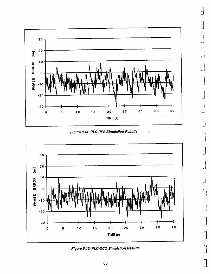
30
.,.,. 20
_=
'" 0
_ -10
-20
-30 I I I I
5 10 15
,I ,i I
1 I I
ii
20 25 30 35 4O
TIME (s)
!.I
l
i.l
Figure 6.14: PLC-PPS Simulation Results
30
... 20
'" 0
-1013,,,
-20
-30
'ILIL L I I ' I __ I
ii
I I I I I I I i
5 10 15 20 25 30 35 40
TIME (s)
_I
Figure 6.15: PLC-DCO Simulation Results
60
J
3

The increase in phase error due to incremental Doppler suggests that incorporating
a Doppler prediction technique which will compensate for this effect can help reduce the
overall phase error for a given supportable bit rate. Alternatively, it could increase the
supportable bit rate for a given overall phase error value. This will be discussed in thenext subsection which explores different techniques for further reducing the overall
phase error.
6.2.3.5 Techniques for reducing phase error in PLC approach
There are two techniques that can be used with the PLC approach to further reduce
the overall phase error. The first technique relies on averaging multiple onboard errormeasurements during the correction period which would reduce the variance of the
random component in the error measurement. The second technique, which was alluded
to earlier, involves residual Doppler prediction and correction to remove thedeterministic fixed bias component from the phase error term.
6.2.3.5.1 Multiple Error Measurements in Correction Period
This is a simple technique which involves taking multiple error measurements in a
correction period and averaging these measurements to reduce the variance of the phaseerror. As long as the error components in the averaged measurements are statistically
independent, the variance of the error will be reduced by the square root of the number of
averaged measurements. Figure 6.16 shows the effect of averaging on the variance of the
error.
1.0
0.8
Z0
t-O
0.6,-,uJ
_" 0.40n-
W
O.2
0.0 I I I , : : : ! , , I I
10
NUMBER OF MEASUREMENTS
Figure 6.16- Effect of Averaging on S_atistieal Phase Error
61

The principaldrawback to the above technique of averaging multiple onboard phase
error measurements isthat a user terminal would have to transmit multiple
synchronization bursts in a correctionperiod. This resultsin increased overhead
associatedwith multiple measurements. However, the payoff in terms of a higher
supportable bitrate may offsetthe required increase in overhead. Technically,the
number ofmeasurements isbetterkept small. However, even as few as three averaged
measurements per correctionperiod could potentiallyreduce the random component of
phase errorby up to 50 % (Figure 6.16).
Although the multiple error measurements naturally must be taken onboard the
satellite,the averaging process may be performed eitheronboard the satelliteor at the
user terminal. In eithercase,the improvement willbe the same.
6.2.3.5.2 Doppler Correction
There are two methods of performing Doppler correction at the user terminal so as to
reduce or eliminate the incremental time delay caused by Doppler during a correction
period. Both methods attempt to predict the magnitude of the Doppler component and to
compensate for it.
The firstmethod, shown in Figure 6.17,isbased on measuring the difference
between two delay values,where a delay value isthe timing offsetbetween the transmit
frame and receiveframe at the user texminal. The measured time differenceis
AT = T_ - 2". = 2(n - 1)pat c
where Pa is the Doppler shift. Small multiple corrections (e.g. 5 times) are then
performed over a correction period to compensate for Pa.
Figure 6.17: Transmit and Receive Frame 71me Difference Measurements
62
1
ii
iii
]
]

I
This Doppler correction method helps reduce the incremental time delay caused by
Doppler roughly by a factor of m, where m is the number of corrections over a clockcorrection period. The Doppler measurement error introduced by this method is very
small on the order of_+0.3 ns.
A linear prediction error is also introduced by assuming that the Doppler variationsare linear in nature. This prediction error is also very small, especially for short
prediction time intervals (on the order of minutes). Figure 6.18 shows the magnitude of
the linear prediction error for Doppler correction as a function of the prediction timeinterval. From this figure, the worst case value over a ten minute prediction interval is
still quite small (around 0.5 ns per second). For shorter prediction time intervals andduring the zero crossing (zero phase) portion of the Doppler cycle, the linear prediction
error becomes negligible.
I
I _ Doppler Phase (0°) _ Doppler Phase (60 °) _" _Doppler Phase (90 °) 'I
1.0E-O3
1.0E-04
1.0E-05 I
1 2 3
= 8 x 10 "9
4 5 6 7 8 9 10
PREDICTION TIME INTERVAL (rain.)
Figure 6.18: Linear Prediction Error for Doppler Correction
An alternativeapproach to Doppler correctionisto use an averaging method where
the onboard phase error measurements over n correctionperiods are averaged to get an
estimate of the average phase error over one correctionperiod. This estimate reflectsthe
Doppler contributionin one correctionperiod. Once an initialestimate isobtained and
compensated forin the phase error corrections,a running average can then be taken to
update an estimate of the residual error and further compensate forit.
The drawback ofthe averaging approach toDoppler predictionisthat itis only
effectiveforrelativelysmall values ofDoppler. For large Doppler values or high speed
applications,the former Doppler predictiontechnique may be used firstthen the
averaging technique may be applied to freetune the estimates given by the first
technique.
63
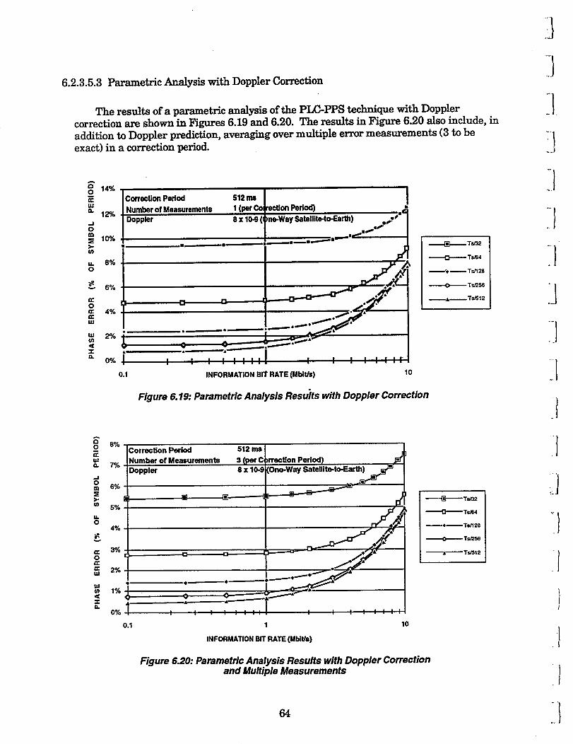
6.2.3.5.3 Parametric Analysis with Doppler Correction
The results of a parametric analysis of the PLC-PPS technique with Doppler
correction are shown in Figures 6.19 and 6.20. The results in Figure 6.20 also include, in
addition to Doppler prediction, averaging over multiple error measurements (3 to be
exact) in a correction period.
_" 14%O
.,Jom
u. 8%o
n-Orr"n-ILl
UJ(;1,<"1-I1.
6%
I
4%
0% i
0.1
Correction Period
Number of Measurements
Doppler
1 (per Co_rectfon Period) q
8 x 10⁻⁹ (The-Way Satellite-to-Earth) /Ts/32
TsJ64
_---/q, -- Ts#128
Tsf256
__j,__Ts/512
Figure 6.19: Parametric Analysis Resets with Doppler Correction
goT.uJn
Jo
_E>.
14.o
a:on.o:
u4
8%
7%
6%
5%
4%
3%
2%
1%
&
o% I
0.1
512 m
Number of Measurements 3q Period)
Doppler Satellite-to-Earth)
_Ts_4
--I--Ts/128
o TrJ25S
_A_Ts/512
• Q,w
I I I I I I II I
1 10
INFORMATION BIT RATE (Mbit/s)
Figure 6.20: Parametric Analysis Results with Doppler Correctionand Multiple Measurements
64
LI.
rll
I
I
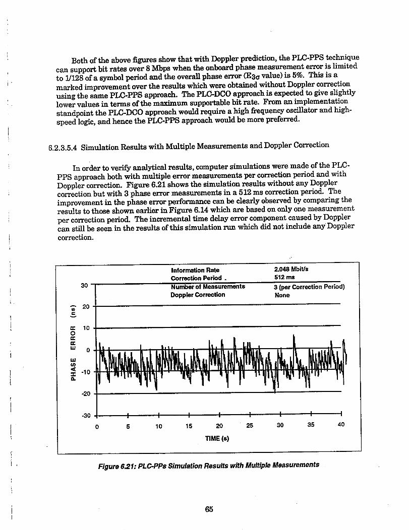
Both of the above figures show that with Doppler prediction, the PLC-PPS technique
can support bit rates over 8 Mbps when the onboard phase measurement error is limited
to 1/128 of a symbol period and the overall phase error (E3a value) is 5%. This is a
marked improvement over the results which were obtained without Doppler correction
using the same PLC-PPS approach. The PLC-DCO approach is expected to give slightlylower values in terms of the maximum supportable bit rate. From an implementation
standpoint the PLC-DCO approach would require a high frequency oscillator and high-
speed logic, and hence the PLC-PPS approach would be more preferred.
6.2.3.5.4 Simulation Results with Multiple Measurements and Doppler Correction
In order to verify analytical results, computer simulations were made of the PLC-
PPS approach both with multiple error measurements per correction period and with
Doppler correction. Figure 6.21 shows the simulation results without any Dopplercorrection but with 3 phase error measurements in a 512 ms correction period. The
improvement in the phase error performance can be clearly observed by comparing theresults to those shown earlier in Figure 6.14 which are based on only one measurement
per correction period. The incremental time delay error component caused by Dopplercan still be seen in the results of this simulation run which did not include any Doppler
correction.
Information Rate 2.048 Mbit/sCorrection Period. 512 ms
30 Number of Measurements 3 (per Correction Period)Doppler Correction None
--" 20CO
uJ 0
-10a.
-20
-3O
'1"I' "I'llI I I I I I I I
0 5 10 15 20 25 30 35 40
TIME (s)
Figure 6.21: PLC-PPs Simulation Results with Multiple Measurements
65

Figure 6.22 shows simulation results which include Doppler correction but with only
one phase error measurements in a 512 ms correction period. These results are similar
in variance to those given in Figure 6.14 earlier except that the average phase error is
now close to zero afar Doppler correction (10 second averaging period for Doppler
correction).
:]
1
I
Information Rate 2.048 Mbit/$Correction Period 512 ms
30 I Number of Measurements 1 (per Correction Period)
t Doppler Correction Yes
20 --- -_ .......
o I I, k . ,
"" -10
-2o .... , -
-30 [ I I I I I I I I
0 5 10 15 20 25 30 3s 40
TIME(s)
i]
]
;1
Figure 6.22: PL C-PPS Simulation Results with Doppler Correction
Finally, Figure 6.23 shows simulation results for 10 Mbps information rate which
include Doppler correction as well as 3 phase error measurements in a 512 ms correctionperiod. These results reflect the best error performance with small phase error variance
and close to zero phase error average after Doppler removal (20 s Doppler prediction
interval).
6.2.c" " Summary of PLC Approach
Table 6.7 shows a summary of the maximum supportable data rates using the PLC-
PPS approach. Slightly lower data rates are also supportable using the PLC-DCO
approach. However, as mentioned earlier, higher frequency DCOs are required which
makes the PLC-DCO technique less attractive compared to the PLC-PPS technique.
66
I
i)
J
i1
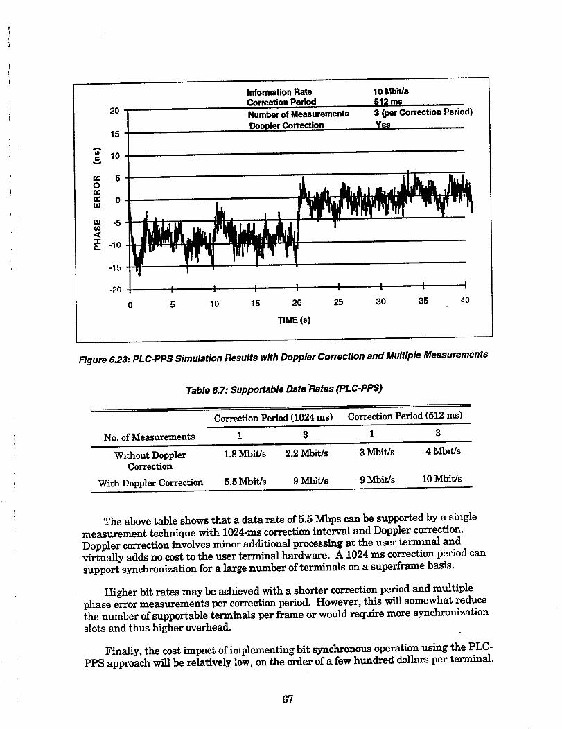
A
reO_eretU
it/
<"v"a=
2O
10
5
0
-5
-10
-15
-20
0
Information RateCorrection Period
Number of Measurements
DopplerCorr_e__ion
10 Mbit/s512 ms3 (per Correction Period)Yes
I I I I I I I I
5 10 15 20 25 30 35 40
TIME (s)
Figure 6.23: PLC-PPS Simulation Results with Doppler Correction and MUltiple Measurements
Table 6.7: Supportable Data "Rates (PLG-PPS)
No. ofMeasurements
Correction Period (1024 ms) Correction Period (512 ms)
1 3 1 3
Without Doppler 1.8 Mbit/s 2.2 Mbit/s 3 Mbit/s 4 Mbit/s
Correction
With Doppler Correction 5.5Mbit/s 9 Mbit/s 9 Mbit/s i0 Mbit/s
The above table shows that a data rate of5.5 Mbps can be supported by a single
measurement technique with 1024-ms correctioninterval and Doppler correction.
Doppler correctioninvolves minor additionalprocessing at the user terminal and
virtuallyadds no costtothe user terminal hardware. A 1024 ms correctionperiod can
support synchronization fora largenumber ofterminals on a superframe basis.
Higher bitrates may be achieved with a shorter correctionperiod and multiple
phase error measurements per correctionperiod. However, thiswillsomewhat reduce
the number ofsupportable terminals per frame or would require more synchronization
slotsand thus higher overhead.
Finally,the costimpact ofimplementing bitsynchronous operation using the PLC-
PPS approach willbe relativelylow,on the order ofa few hundred dollarsper terminal.
67
6.3 Summary of Timing Analysis
Based on the analysis and simulation results presented in this section, the followingconclusions can be made. The independent clock (IC) approach is more complex and
yields worse performance than the phase locked clock (PLC) technique. The PLC system
can be implemented using either a programmable phase shifter (PPS) or a digitalcontrolled oscillator (DCO). The PPS provides slightly better performance than the DCO
and is not restricted by the DCO high frequency limitations. The information bit rates
supported by a bit synchronous system can be from about 2 MbitYs to about 101VIbps for
QPSK modulation with rate-l/2 coding depending on the error correction techniqueselected. This is based on the worst-case phase error of 5 - 6 percent of a symbol period.
Even higher bit rates can be accommodated but at the expense of higher performance
degradation (more than 0.5 dB loss due to timing misalignment).
68
]
Jl
]
]
]
_l
Jl
1
Jl
]
I
]

Section 7
Conclusions
t_
i.
A bit synchronous MF-TDMA system was initially deemed to be a high risk system
concept that might accompany a number of critical system design issues. Throughextensive analysis and simulation performed in the present study, this synchronization
concept is found to be a practical as well as viable technique that will provide numerous
advantages over conventional TDMA synchronization. The potential benefits of a bit
synchronous system are simpler implementation of onbeard multicarrier demultiplexersand demodulators, higher flame efficiency, smaller onboard buffer size, and smaller
onboard processing/switching delay. In addition, the baseline network architecturenecessitates the use of a bit synchronous technique; otherwise, frame efficiency will be
reduced to about 50 percent, or a frame length must be increased by an order of
magnitude to achieve a reasonable frame efficiency.
The bit synchronous technique allows demultiplexer operation with one output
sample per symbol and further eliminates interpolation filtering. The impact on onboardhardware will be the reduction of mass and power by a factor of 2/3 relative to the
asynchronous system. In addition, this technique eliminates a timing recovery andcorrection function in the multicarrier demodulator implementation and results in about
a 50-percent reduction in mass and power. These estimates are based on the
computational complexity of these devices, and actual reductions may be less than thosecited above due to supporting logic circuits and PC boards common to both techniques.
The impact of a bit synchronous system on TDMA frame design is significant. For
example, a conventional TDMA system with a variable burst length requires a TDMAframe length of about 28 ms to achieve a 90-percent frame efficiency at a bit rate of 2.048
Mbit/s and 40 bursts per frame, while the bit synchronous system only needs a 3-ms
frame length to provide the same performance. This implies that the latter
synchronization technique reduces the onboard buffer size and processing delay to aboutone-tenth of those of the conventional system. Also, the user terminal buffer size is
reduced accordingly. Similar improvements, though not so drastic as above, can be
observed for a single-channel-per-burst TDMA system with a bit synchronous technique.
Two types of clock control techniques to align transmitted TDMA bursts with anonboard reference clock were analyzed in the report. The first technique employs an
independent user terminal clock (IC technique) and a simple prediction circuit toestimate clock correction values. The second technique derives a transmit clock from a
received downlink clock by a phase lock technique (PLC technique). The PLC technique
is simpler than the IC approach and provides a precise timing alignment with theonboard clock with an accuracy of about 5-percent of a symbol period. Timing correction
is performed using either a programmable phase shifter (PPS) or a digitally controlledoscillator (DCO), where the former yields a slightly better accuracy. These devices are
relatively inexpensive and contribute an additional few hundred dollars to the overall
terminal cost.
69

A simple PLC technique, which is based on single phase error measurement without
Doppler compensation, can support a bit rate of up to 3 Mbit/s. With multiple phaseerror measurements and Doppler compensation, the supportable bit rate exceeds 10
Mbit/s. These results were verified by analysis and computer simulation. The impact of
higher bit rates on the user terminal cost is virtually none for the PPS implementationbut will be higher for the DCO technique due to high-speed operation of oscillator and
programmable divider circuits.
Based on the present study, two areas have been identified for future work. The
first area is to perform a detailed analysis and simulation of onboard carrier and clock
recovery circuit performance, including simulation of communication channel and
demultiplexer/demodulator processing functions. For onboard burst recovery, thecurrent study used the results published in the literature and a simple analysis. Thus,
the proposed study will be useful in validating and/or refining onbeard processorfunctions and performance. The second area of future work is to develop a proof-of-
concept hardware device to perform user clock correction, using either a PPS or a DCO
technique. This will be a necessary step of implementing a bit synchronous system in the
future advanced onboard processing satellite.
7O
_J
I
11
_i
!
J
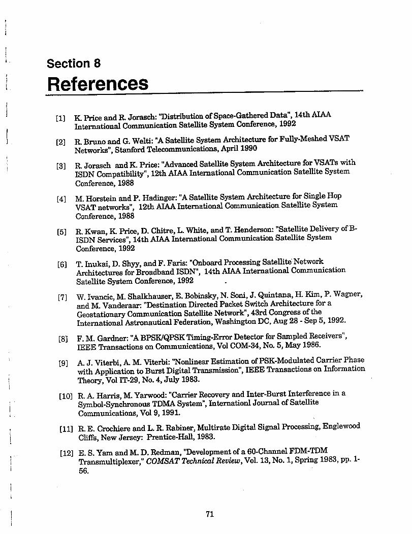
Section 8
References
[11]
[12]
[1] I_ Price and R. Jorasch: "Distribution of Space-Gathered Data", 14th AIAAInternational Communication Satellite System Conference, 1992
[2] R. Bruno and G. Welti: "A Satellite System Architecture for Fully-Meshed VSATNetworks", Stanford Telecommunications, April 1990
[3] R. Jorasch and K. Price: "Advanced Satellite System Architecture for VSATs with
ISDN Compatibility", 12th AIAA International Communication Satellite System
Conference, 1988
[4] M. Horstein and P. Hadinger: "A Satellite System Architecture for Single Hop
VSAT networks", 12th AIAA International Communication Satellite System
Conference, 1988
[5] R. Kwan, K. Price, D. Chitre, L. White, and T. Henderson: "Satellite Delivery of B-ISDN Services", 14th AIAA International Communication Satellite System
Conference, 1992
[6] T. Inukai, D. Shyy, and F. Faris: "Onboard Processing SatelliteNetworkArchitectures for Broadband ISDN", 14th AIAA International Communication
Satellite System Conference, 1992
[7] W. Ivancic, M. Shalkhanser, E. Bobinsky, N. Soni, J. Quintana, H. Kim, P. Wagner,and M. Vanderaar: "Destination Directed Packet Switch Architecture for a
Geostationary Commum'cation Satellite Network", 43rd Congress of theInternational Astronautical Federation, Washington DC, Aug 28 - Sep 5, 1992.
[8] F.M. Gardner: "A BPSK/QPSK Timing-Error Detector for Sampled Receivers",IEEE Transactions on Communications, Vol COM-34, No. 5, May 1986.
[9] A.J. Viterbi, A. M. Viterbi: '_Nonlinear Estimation of PSK-Modulated Carrier Phase
with Application to Burst Digital Transmission", IEEE Transactions on Information
Theory, Vol IT-29, No. 4, July 1983.
[10] R.A. Harris, M. Yarwood: "Carrier Recovery and Inter-Burst Interference in a
Symbol-Synchronous TDMA System", Internationl Journal of Satellite
Communications, Vol 9, 1991.
R. E. Crochiere and L. R. Rabiner, Multirate Digital Signal Processing, Englewood
Cliffs, New Jersey: Prentice-Hall, 1983.
E. S. Yam and M. D. Redman, "Development of a 60-Channel FDM-TDM
Transmultiplexer," COMSAT Technical Review, Vol. 13, No. 1, Spring 1983, pp. 1-
56.
71

[13]
[14]
[15]
[16]
S. I. Sayegh, "DSP MCDs for Future IBS/IDR Services," 2nd International
Workshop on Digital Signal Processing Techniques Applied to Space
Communications, Turin, Italy, September 1990.
T. Inukal and S. J. CampaneUa, "Optimal Onboard Clock Control," IEEE Journal onSelected Areas in Communications, Vol. SAC-l, No. 1, pp.208-213, January 1983.
T. Inukal and S. J. Campanella, "Onboard Clock Correction for SS-DMA and
Baseband Processing Satellites," COMSAT Technical Review, Vol. 11, No. 1, pp. 77-
102, Spring 1981.
M. Morikura and S. Kate, "Study on Control Interval of Onboard Master Clock,"
IEICE Trans., vol. J70-B, No. 3, March 1987.
J
:l
:}
:]
:]
:]
72
i]

Form Approved
REPORT DOCUMENTATION PAGE OMBNo.0704-0188
_, _s o_. of_fo_ _ =_,_ '_a_ 1_, _ r_e ,_.Q _ _m_fo,_w_g _ :: _ _e _'_'_o,_ _Pubhc.report,ng burd.en ........... .4 reviewi_ me collect" n f information. Send commenr.s regaratng _ ouroen .es.umal or any .l_'U._o
Davis Highway. Suite 1204. Arlington. VA _z._-_, =,,J -_ - ....... "= -o
1. AGENCY USE ONLY (Leave blank) 2. REPORT DATE 3. REPORT TYPE AND DATES COVERED
January 28, 1994
4. TITLE AND SUBTITLE
Modulation and Synchronization Techniques for MF-TDMA System
6. AUTHOR(S)
Faris Faris, Thomas Inukai and Soheil Sayegh
7. PERFORMING ORGANIZATION NAME(S) AND ADDRESS(ES)
COMSAT Laboratories22300 COMSAT Drive
Clarksburg, MD 20871
9. SPONSORING/MONITORINGAGENCYNAMES(S)ANDADDRESS(ES)
National Aeronautics and Space Administration (NASA)
Lewis Research Center21000 Brookpark RoadCleveland, OH 44135
11. SUPPLEMENTARY NOTES
Heechul Kim(216) 433-8698
Space Electronics Division, NASA-LeRC12= DISTRIBUTION/AVAILABILITY STATEMENT
S. FUNDING NUMBERS
RTCP 506-72-21
8. PERFORMING ORGANIZATIONREPORTNUMBER
E-8324
10. SPONSORING/MON_ORING
AGENCYREPORTNUMBER
CR-194448
12b. Dk_IHIBUTION CODE
13. ABSTRACT (Maximum 200 words)
This report addresses modulation and synchronization techniques for a multifrequency time-division-multiple-access (MF-TDMA) system with onboard baseband processing. The types of synchronizationtechniques analyzed are asynchronous (conventional) TDMA, preambleless asynchronous TDMA, bitsynchronous timing with a preamble, and preambleless bit synchronous timing. Among these alternatives,preambleless bit synchronous timing simplifies onboard multicarrier demultiplexer/demodulator designs(about 2:1 reduction in mass and power), requires smaller onboard buffers (10:1 ~ 3:1 reduction in size),
and provides better frame efficiency as well as lower onboard processing delay. Analysis and computersimulation illustrate that this technique can support a bit rate of up to 10 Mbit/s (or higher) with proper
selection of design parameters. High bit rate transmission may require Doppler compensation and
multiple phase error measurements. The recommended modulation technique for bit synchronous timingis coherent QPSK with differential encoding for the uplink and coherent QPSK for the downlink.
14. SUBJECT TERMS
Modulation, Onboard Processing, Satellite Network, Synchronization,TDMA, Timing
17. SECURITY CLASSIFICATION
OF REPORT
Uncl__ified
NSN 7540-01-280-5500
18. SECURITY CLASSIFICATION
OF THIS PAGE
Unclassified
19. SECURITY CLASSIRCATIONOF ABSTRACT
Unclassified
15. NUMBER OF PAGES
7216. PRICE CODE
20. UMITATIONOFABSi-NACT
Unlimited Distribution
Standard Form 298 (Rev. 2-89)
Prescribed by ANSI Std. Z39-18_QR.lrI_
Related Documents