1622 IEEE TRANSACTIONS ON INDUSTRIAL ELECTRONICS, VOL. 61, NO. 3, MARCH 2014 Modular Realization of Capacitive Converters Based on General Transposed Series–Parallel and Derived Topologies Yuval Beck, Member, IEEE, S. Singer, Member, IEEE, and L. Martinez-Salamero, Senior Member, IEEE Abstract—The realization of capacitive converters based on a modular approach is presented and analyzed in this paper. The converters are based on topologies with identical capacitors. First, the switching network (SN) of a basic series–parallel topology is presented. The analysis reveals the assembly and growth rules for expanding the topology to any number of capacitors. Subse- quently, the SN for the more versatile and complex general trans- posed series–parallel (GTSP) topology is presented. The topology is expanded by defining a basic cell comprising a capacitor and five peripheral switches. The expansion of this converter improves its performance by ameliorating accuracy and regulation in the dc/dc voltage ratio. The control schemes of these converters are also presented with emphasis on the GTSP topology, whose switches are not assigned in advance. The control scheme for achieving the desired voltage ratio is described. A five-capacitor converter with its control is built to illustrate the theory in open-loop mode, which provides experimental results that are in full agreement with the analytical predictions. Index Terms—Circuit topology, dc–dc power conversion, inte- grated circuits, multiplying circuits, switched systems. I. I NTRODUCTION T HERE has been much interest recently in capacitive- based converters because of their capability for integra- tion [1], [2]. In order to enhance the performance of such converters, voltage regulation has been also researched [3], [4]. In the literature, a few switched-capacitor (SC) topologies have been presented and analyzed [5]. Generally, earlier works have analyzed topologies for either voltage multiplying [6]–[8], reduction [3], or inversion capabilities [9]. A further example described in [10] is a topology that yields multiple conver- sion ratios by an algebraic binary method. The functioning of capacitive converters is based on a similar principle; a group of capacitors is interconnected in some way in the charging state and interconnected in another way in the discharging state. The transition between the charging and discharging Manuscript received March 8, 2012; revised October 31, 2012 and January 30, 2013; accepted March 5, 2013. Date of publication April 12, 2013; date of current version August 23, 2013. This work was supported in part by the Israeli Science Foundation under Grant 1328/12. Y. Beck is with the Electrical Engineering Faculty, Holon Institute of Technology, Holon 58102, Israel (e-mail: [email protected]). S. Singer is with the School of Electrical Engineering, Tel Aviv University, Tel Aviv 6997801, Israel (e-mail: [email protected]). L. Martinez-Salamero is with the Department of Electrical, Electronic, and Automatic Control Engineering, Rovira i Virgili University, 43003 Tarragona, Spain (e-mail: [email protected]). Color versions of one or more of the figures in this paper are available online at http://ieeexplore.ieee.org. Digital Object Identifier 10.1109/TIE.2013.2257144 states implies input/output voltage conversion. The transition between the charging and discharging states is achieved by means of a high-frequency switching network (SN). (A high switching frequency implies a frequency that is high enough, such that the relation between the voltage drop and the output voltage is ΔV/V 1.) The SN has two tasks: 1) to form charging and discharging graphs (here, graph refers to a way of presenting the connectivity scheme of the elements, as is done in network analysis theory); and 2) to make a transition between them at a high switching frequency. For more complex topologies that enable a multitude of transfer ratios, the SN forms a multitude of pairs of charge/discharge graphs, each pair determining a voltage or current transfer ratio. Under adequate control, the appropriate configuration of the dc–dc converter is set according to the target transfer voltage ratio. Control enables the transition from one pair to another by means of the SN. The construction of the SN might be quite complex; thus, this paper presents a systematic approach based on “modular growth,” which has been developed in order to overcome this difficulty. It should be noted that a variety of modular topologies for the realization of converters has been presented in previous works. In [11] and [12], a generalized approach for a bidirectional power flow dc/dc converter is presented. In [13] and [14], the modular approach is implemented in multilevel dc/dc converters. The modularity of converters can be seen in the converter internal switching schemes, as shown in [15], or when constructing a converter that consists of various converters, such as interleaved converters, as demonstrated in [16]. Nevertheless, the modular approach is not suitable for all systems, and for any specific system, there is no guarantee that it would be suitable. This paper presents the basic cell of the modular structure, as well as the connectivity between the cells for forming the functionality of the general transposed series–parallel (GTSP) topology. In the initial stages of GTSP development [4], [17], the research focused on the structure of the topology, the calculation of the possible number of transfer ratios (as a function of the number of capacitors), their values, and the distribution function of those transfer ratios with special attention to the range that implies “fine-tuning” (regulation) capabilities. At that stage, no attention was paid to the synthesis of the SN, which would enable the realization of the topology, as it was assumed that it would be an easy task to find some SN that would work. In this paper, the development of the modular structure that is suitable for GTSP realization is described. This includes new 0278-0046 © 2013 IEEE

Welcome message from author
This document is posted to help you gain knowledge. Please leave a comment to let me know what you think about it! Share it to your friends and learn new things together.
Transcript
1622 IEEE TRANSACTIONS ON INDUSTRIAL ELECTRONICS, VOL. 61, NO. 3, MARCH 2014
Modular Realization of Capacitive Converters Basedon General Transposed Series–Parallel
and Derived TopologiesYuval Beck, Member, IEEE, S. Singer, Member, IEEE, and L. Martinez-Salamero, Senior Member, IEEE
Abstract—The realization of capacitive converters based on amodular approach is presented and analyzed in this paper. Theconverters are based on topologies with identical capacitors. First,the switching network (SN) of a basic series–parallel topology ispresented. The analysis reveals the assembly and growth rulesfor expanding the topology to any number of capacitors. Subse-quently, the SN for the more versatile and complex general trans-posed series–parallel (GTSP) topology is presented. The topologyis expanded by defining a basic cell comprising a capacitor and fiveperipheral switches. The expansion of this converter improves itsperformance by ameliorating accuracy and regulation in the dc/dcvoltage ratio. The control schemes of these converters are alsopresented with emphasis on the GTSP topology, whose switchesare not assigned in advance. The control scheme for achieving thedesired voltage ratio is described. A five-capacitor converter withits control is built to illustrate the theory in open-loop mode, whichprovides experimental results that are in full agreement with theanalytical predictions.
Index Terms—Circuit topology, dc–dc power conversion, inte-grated circuits, multiplying circuits, switched systems.
I. INTRODUCTION
THERE has been much interest recently in capacitive-based converters because of their capability for integra-
tion [1], [2]. In order to enhance the performance of suchconverters, voltage regulation has been also researched [3],[4]. In the literature, a few switched-capacitor (SC) topologieshave been presented and analyzed [5]. Generally, earlier workshave analyzed topologies for either voltage multiplying [6]–[8],reduction [3], or inversion capabilities [9]. A further exampledescribed in [10] is a topology that yields multiple conver-sion ratios by an algebraic binary method. The functioning ofcapacitive converters is based on a similar principle; a groupof capacitors is interconnected in some way in the chargingstate and interconnected in another way in the dischargingstate. The transition between the charging and discharging
Manuscript received March 8, 2012; revised October 31, 2012 andJanuary 30, 2013; accepted March 5, 2013. Date of publication April 12, 2013;date of current version August 23, 2013. This work was supported in part bythe Israeli Science Foundation under Grant 1328/12.
Y. Beck is with the Electrical Engineering Faculty, Holon Institute ofTechnology, Holon 58102, Israel (e-mail: [email protected]).
S. Singer is with the School of Electrical Engineering, Tel Aviv University,Tel Aviv 6997801, Israel (e-mail: [email protected]).
L. Martinez-Salamero is with the Department of Electrical, Electronic, andAutomatic Control Engineering, Rovira i Virgili University, 43003 Tarragona,Spain (e-mail: [email protected]).
Color versions of one or more of the figures in this paper are available onlineat http://ieeexplore.ieee.org.
Digital Object Identifier 10.1109/TIE.2013.2257144
states implies input/output voltage conversion. The transitionbetween the charging and discharging states is achieved bymeans of a high-frequency switching network (SN). (A highswitching frequency implies a frequency that is high enough,such that the relation between the voltage drop and the outputvoltage is ΔV/V � 1.) The SN has two tasks: 1) to formcharging and discharging graphs (here, graph refers to a wayof presenting the connectivity scheme of the elements, as isdone in network analysis theory); and 2) to make a transitionbetween them at a high switching frequency. For more complextopologies that enable a multitude of transfer ratios, the SNforms a multitude of pairs of charge/discharge graphs, each pairdetermining a voltage or current transfer ratio. Under adequatecontrol, the appropriate configuration of the dc–dc converter isset according to the target transfer voltage ratio. Control enablesthe transition from one pair to another by means of the SN.
The construction of the SN might be quite complex; thus,this paper presents a systematic approach based on “modulargrowth,” which has been developed in order to overcomethis difficulty. It should be noted that a variety of modulartopologies for the realization of converters has been presentedin previous works. In [11] and [12], a generalized approachfor a bidirectional power flow dc/dc converter is presented.In [13] and [14], the modular approach is implemented inmultilevel dc/dc converters. The modularity of converters canbe seen in the converter internal switching schemes, as shownin [15], or when constructing a converter that consists of variousconverters, such as interleaved converters, as demonstrated in[16]. Nevertheless, the modular approach is not suitable forall systems, and for any specific system, there is no guaranteethat it would be suitable. This paper presents the basic cell ofthe modular structure, as well as the connectivity between thecells for forming the functionality of the general transposedseries–parallel (GTSP) topology. In the initial stages of GTSPdevelopment [4], [17], the research focused on the structure ofthe topology, the calculation of the possible number of transferratios (as a function of the number of capacitors), their values,and the distribution function of those transfer ratios with specialattention to the range that implies “fine-tuning” (regulation)capabilities. At that stage, no attention was paid to the synthesisof the SN, which would enable the realization of the topology,as it was assumed that it would be an easy task to find some SNthat would work.
In this paper, the development of the modular structure thatis suitable for GTSP realization is described. This includes new
0278-0046 © 2013 IEEE
BECK et al.: REALIZATION OF CAPACITIVE CONVERTERS BASED ON GTSP AND DERIVED TOPOLOGIES 1623
formation of a basic module comprising a single capacitor, pe-ripheral switches, their interconnections, and connecting ports.It also includes new determination of the minimum number ofswitching elements in the switching cell.
The main innovation presented in this paper is embodiedin the idea of using the modular concept for realization of acapacitive converter based on the GTSP topology. In addition,the formation of a suitable basic module, the construction ofthe appropriate modular structure, and the development of theswitching control unit are totally new. This paper systemati-cally describes the thought processes behind the evolution ofthe converter’s network structure, which has a multitude ofinput/output voltage ratios. The dynamics of the transitions be-tween the various voltage ratios are analyzed, and experimentalresults are presented and discussed.
II. MODULAR GROWTH OF CAPACITIVE CONVERTERS
A. Loss-Free Topologies
Among SC topologies, there is a family of topologies inwhich all capacitors have an equal value of capacitance, whichcan be assumed to be loss free (in principle only), provided thatsome conditions described below are fulfilled.
1) The voltage ripple is negligible: ΔV −→ 0. This is im-plied by a high switching frequency: fswitching −→ ∞.
2) Switch losses are negligible: Pswitching −→ ∞ (conduc-tion losses, switching losses, etc.).
3) Capacitors are ideal with no losses (equivalent seriesresistance (ESR), etc.).
Such topologies are described in [4], [18], and [19]. Thesimple series–parallel (SP) topology, in which the capaci-tors are charged in parallel and discharged in series (or viceversa), belongs to that family. There are other capacitive-basedconverters, which have inherent principal losses due to thesignificant voltage difference on the capacitors in the variousoperating states [20], [21].
The above statement does not imply that practical circuitsbased on that topology are loss free. In practical circuits, theswitching frequency is finite, which implies a nonzero voltagedrop ΔV on the capacitors, which, in turn, implies losses; inaddition, there are always some switching losses.
In all the capacitive topologies, graphs of interconnectionsin both charging and discharging states are formed. The loss-free topologies (and GTSP in particular) are characterizedby the inversion of the series/parallel interconnections of thecapacitors in the charging and discharging phases. This can beseen as transferring the topology through a Gyrator [22]–[24].The simplest example is in the SP topology, in which a seriesgraph in the charging state is transferred to a parallel graph inthe discharging state. In the matrix converter, rows turn intocolumns from charging to discharging. GTSP is another evolu-tion of the SP and matrix converters [24], [25]. This topology isthe most versatile topology with a reduced number of capacitorsand switches, including a large number of input/output voltageratios [4], [17]. Further examination of this topology yields theconclusion that this topology is a general case, which includesthe SP and matrix topologies as particular cases.
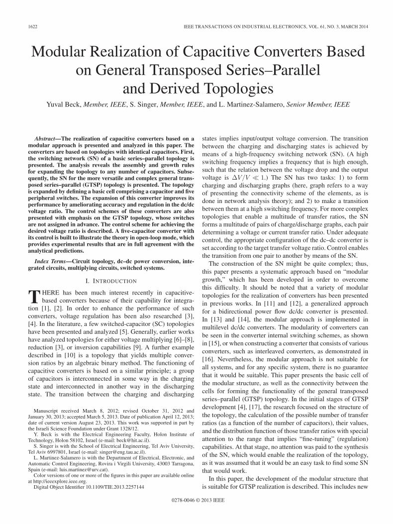
Fig. 1. (a) Charging state of three capacitors in parallel and its graph.(b) Discharging state of three capacitors in series and its graph.
It should be noted that although the charging and dischargingstates are somewhat virtual, they do not have self-existence andare formed by the SN. The SN has the following tasks regardingthese graphs.
1) To create these graphs.2) To switch between the charging and discharging graphs.3) In more complex topologies, when the number of voltage
ratios is large, the SN provides the ability to choosebetween various ratios.
The assembly of these switching topologies and the controlof the SN from one state to the other is described in thefollowing sections.
B. Graph Presentation of Capacitive Converters
The simplest case of a capacitive converter is the SP con-verter. The voltage transfer ratio in the SP is n, where n denotesthe number of capacitors in the topology.
The arrangement of three capacitors in charging and dis-charging (C/D) states and the C/D graphs of the SP topologyare presented in Fig. 1.
The lower graphs shown in Fig. 1 are a presentation ofthe connectivity of each circuit. These graphs are obtained byreplacing each component by a line, and the obtained graphrepresents the connectivity between the components. Fig. 1(a)represents the charging-state connections of the capacitor, andFig. 1(b) represents the discharging-state connections.
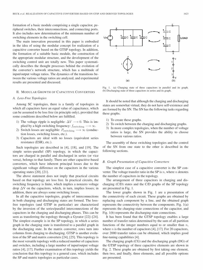
It has been found that the GTSP topology enables a largenumber of transfer ratios determined by the sum of all partitionfunctions of the integer numbers equal to or smaller than n,where n is the number of capacitors [4], [17]. For 20 capacitors,over 2000 transfer ratios can be obtained, which implies goodfine-tuning capabilities [4].
The charging graph (CG) and the discharging graph (DG) ofthe GTSP topology of three capacitive elements are shown inFig. 2. These graphs are obtained by first taking one element,then two, and finally, three elements, and all possible optionsare presented.
1624 IEEE TRANSACTIONS ON INDUSTRIAL ELECTRONICS, VOL. 61, NO. 3, MARCH 2014
Fig. 2. All possible charging and discharging graphs of a three-capacitorGTSP.
C. GTSP SN Realization Approach
The synthesis of the SN was first based on a heuristicmethod (trial and error up to success). In the GTSP topology,an increased number of transfer ratios can be achieved by amodest increase in the number of capacitors n, because thenumber of transfer ratio options is the sum of all partitionfunctions up to n. This number significantly increases as nincreases [17]. Unfortunately, the increase in the number ofcapacitors implies an exponential increase in the complexity ofthe synthesis problem, which makes the heuristic constructionmethod unacceptable. This was the motivation for finding asystematic approach for the realization of converters based onthis topology.
After a long search for a suitable synthesis method (includingtrying some that failed), we decided to base the realization ofthe topology on the modular approach.
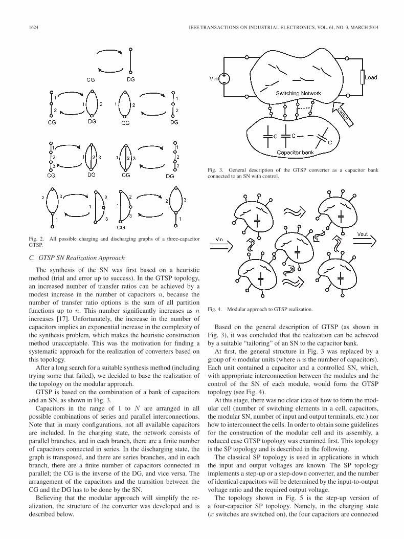
GTSP is based on the combination of a bank of capacitorsand an SN, as shown in Fig. 3.
Capacitors in the range of 1 to N are arranged in allpossible combinations of series and parallel interconnections.Note that in many configurations, not all available capacitorsare included. In the charging state, the network consists ofparallel branches, and in each branch, there are a finite numberof capacitors connected in series. In the discharging state, thegraph is transposed, and there are series branches, and in eachbranch, there are a finite number of capacitors connected inparallel; the CG is the inverse of the DG, and vice versa. Thearrangement of the capacitors and the transition between theCG and the DG has to be done by the SN.
Believing that the modular approach will simplify the re-alization, the structure of the converter was developed and isdescribed below.
Fig. 3. General description of the GTSP converter as a capacitor bankconnected to an SN with control.
Fig. 4. Modular approach to GTSP realization.
Based on the general description of GTSP (as shown inFig. 3), it was concluded that the realization can be achievedby a suitable “tailoring” of an SN to the capacitor bank.
At first, the general structure in Fig. 3 was replaced by agroup of n modular units (where n is the number of capacitors).Each unit contained a capacitor and a controlled SN, which,with appropriate interconnection between the modules and thecontrol of the SN of each module, would form the GTSPtopology (see Fig. 4).
At this stage, there was no clear idea of how to form the mod-ular cell (number of switching elements in a cell, capacitors,the modular SN, number of input and output terminals, etc.) norhow to interconnect the cells. In order to obtain some guidelinesfor the construction of the modular cell and its assembly, areduced case GTSP topology was examined first. This topologyis the SP topology and is described in the following.
The classical SP topology is used in applications in whichthe input and output voltages are known. The SP topologyimplements a step-up or a step-down converter, and the numberof identical capacitors will be determined by the input-to-outputvoltage ratio and the required output voltage.
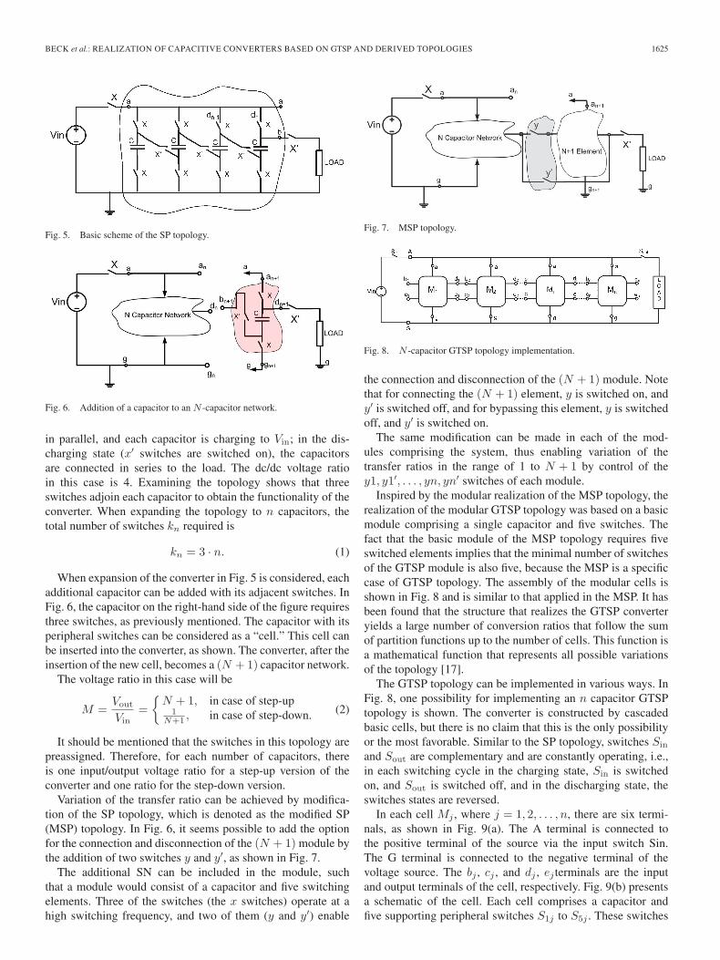
The topology shown in Fig. 5 is the step-up version ofa four-capacitor SP topology. Namely, in the charging state(x switches are switched on), the four capacitors are connected
BECK et al.: REALIZATION OF CAPACITIVE CONVERTERS BASED ON GTSP AND DERIVED TOPOLOGIES 1625
Fig. 5. Basic scheme of the SP topology.
Fig. 6. Addition of a capacitor to an N -capacitor network.
in parallel, and each capacitor is charging to Vin; in the dis-charging state (x′ switches are switched on), the capacitorsare connected in series to the load. The dc/dc voltage ratioin this case is 4. Examining the topology shows that threeswitches adjoin each capacitor to obtain the functionality of theconverter. When expanding the topology to n capacitors, thetotal number of switches kn required is
kn = 3 · n. (1)
When expansion of the converter in Fig. 5 is considered, eachadditional capacitor can be added with its adjacent switches. InFig. 6, the capacitor on the right-hand side of the figure requiresthree switches, as previously mentioned. The capacitor with itsperipheral switches can be considered as a “cell.” This cell canbe inserted into the converter, as shown. The converter, after theinsertion of the new cell, becomes a (N + 1) capacitor network.
The voltage ratio in this case will be
M =Vout
Vin=
{N + 1, in case of step-up
1N+1 , in case of step-down. (2)
It should be mentioned that the switches in this topology arepreassigned. Therefore, for each number of capacitors, thereis one input/output voltage ratio for a step-up version of theconverter and one ratio for the step-down version.
Variation of the transfer ratio can be achieved by modifica-tion of the SP topology, which is denoted as the modified SP(MSP) topology. In Fig. 6, it seems possible to add the optionfor the connection and disconnection of the (N + 1) module bythe addition of two switches y and y′, as shown in Fig. 7.
The additional SN can be included in the module, suchthat a module would consist of a capacitor and five switchingelements. Three of the switches (the x switches) operate at ahigh switching frequency, and two of them (y and y′) enable
Fig. 7. MSP topology.
Fig. 8. N -capacitor GTSP topology implementation.
the connection and disconnection of the (N + 1) module. Notethat for connecting the (N + 1) element, y is switched on, andy′ is switched off, and for bypassing this element, y is switchedoff, and y′ is switched on.
The same modification can be made in each of the mod-ules comprising the system, thus enabling variation of thetransfer ratios in the range of 1 to N + 1 by control of they1, y1′, . . . , yn, yn′ switches of each module.
Inspired by the modular realization of the MSP topology, therealization of the modular GTSP topology was based on a basicmodule comprising a single capacitor and five switches. Thefact that the basic module of the MSP topology requires fiveswitched elements implies that the minimal number of switchesof the GTSP module is also five, because the MSP is a specificcase of GTSP topology. The assembly of the modular cells isshown in Fig. 8 and is similar to that applied in the MSP. It hasbeen found that the structure that realizes the GTSP converteryields a large number of conversion ratios that follow the sumof partition functions up to the number of cells. This function isa mathematical function that represents all possible variationsof the topology [17].
The GTSP topology can be implemented in various ways. InFig. 8, one possibility for implementing an n capacitor GTSPtopology is shown. The converter is constructed by cascadedbasic cells, but there is no claim that this is the only possibilityor the most favorable. Similar to the SP topology, switches Sin
and Sout are complementary and are constantly operating, i.e.,in each switching cycle in the charging state, Sin is switchedon, and Sout is switched off, and in the discharging state, theswitches states are reversed.
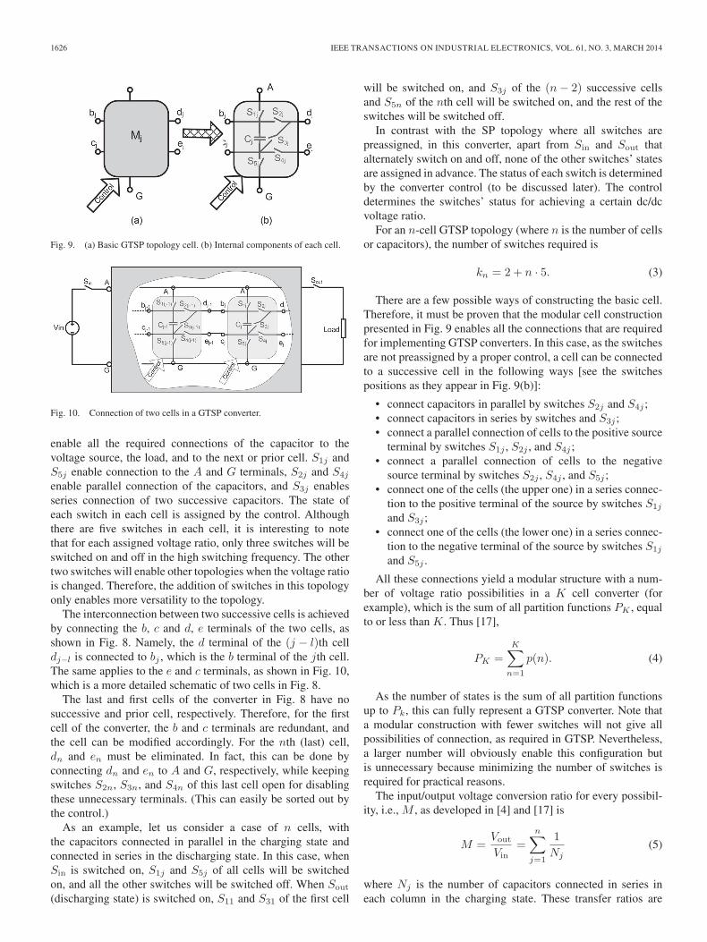
In each cell Mj , where j = 1, 2, . . . , n, there are six termi-nals, as shown in Fig. 9(a). The A terminal is connected tothe positive terminal of the source via the input switch Sin.The G terminal is connected to the negative terminal of thevoltage source. The bj , cj , and dj , ej terminals are the inputand output terminals of the cell, respectively. Fig. 9(b) presentsa schematic of the cell. Each cell comprises a capacitor andfive supporting peripheral switches S1j to S5j . These switches
1626 IEEE TRANSACTIONS ON INDUSTRIAL ELECTRONICS, VOL. 61, NO. 3, MARCH 2014
Fig. 9. (a) Basic GTSP topology cell. (b) Internal components of each cell.
Fig. 10. Connection of two cells in a GTSP converter.
enable all the required connections of the capacitor to thevoltage source, the load, and to the next or prior cell. S1j andS5j enable connection to the A and G terminals, S2j and S4j
enable parallel connection of the capacitors, and S3j enablesseries connection of two successive capacitors. The state ofeach switch in each cell is assigned by the control. Althoughthere are five switches in each cell, it is interesting to notethat for each assigned voltage ratio, only three switches will beswitched on and off in the high switching frequency. The othertwo switches will enable other topologies when the voltage ratiois changed. Therefore, the addition of switches in this topologyonly enables more versatility to the topology.
The interconnection between two successive cells is achievedby connecting the b, c and d, e terminals of the two cells, asshown in Fig. 8. Namely, the d terminal of the (j − l)th celldj−l is connected to bj , which is the b terminal of the jth cell.The same applies to the e and c terminals, as shown in Fig. 10,which is a more detailed schematic of two cells in Fig. 8.
The last and first cells of the converter in Fig. 8 have nosuccessive and prior cell, respectively. Therefore, for the firstcell of the converter, the b and c terminals are redundant, andthe cell can be modified accordingly. For the nth (last) cell,dn and en must be eliminated. In fact, this can be done byconnecting dn and en to A and G, respectively, while keepingswitches S2n, S3n, and S4n of this last cell open for disablingthese unnecessary terminals. (This can easily be sorted out bythe control.)
As an example, let us consider a case of n cells, withthe capacitors connected in parallel in the charging state andconnected in series in the discharging state. In this case, whenSin is switched on, S1j and S5j of all cells will be switchedon, and all the other switches will be switched off. When Sout
(discharging state) is switched on, S11 and S31 of the first cell
will be switched on, and S3j of the (n− 2) successive cellsand S5n of the nth cell will be switched on, and the rest of theswitches will be switched off.
In contrast with the SP topology where all switches arepreassigned, in this converter, apart from Sin and Sout thatalternately switch on and off, none of the other switches’ statesare assigned in advance. The status of each switch is determinedby the converter control (to be discussed later). The controldetermines the switches’ status for achieving a certain dc/dcvoltage ratio.
For an n-cell GTSP topology (where n is the number of cellsor capacitors), the number of switches required is
kn = 2 + n · 5. (3)
There are a few possible ways of constructing the basic cell.Therefore, it must be proven that the modular cell constructionpresented in Fig. 9 enables all the connections that are requiredfor implementing GTSP converters. In this case, as the switchesare not preassigned by a proper control, a cell can be connectedto a successive cell in the following ways [see the switchespositions as they appear in Fig. 9(b)]:
• connect capacitors in parallel by switches S2j and S4j ;• connect capacitors in series by switches and S3j ;• connect a parallel connection of cells to the positive source
terminal by switches S1j , S2j , and S4j ;• connect a parallel connection of cells to the negative
source terminal by switches S2j , S4j , and S5j ;• connect one of the cells (the upper one) in a series connec-
tion to the positive terminal of the source by switches S1j
and S3j ;• connect one of the cells (the lower one) in a series connec-
tion to the negative terminal of the source by switches S1j
and S5j .
All these connections yield a modular structure with a num-ber of voltage ratio possibilities in a K cell converter (forexample), which is the sum of all partition functions PK , equalto or less than K. Thus [17],
PK =K∑
n=1
p(n). (4)
As the number of states is the sum of all partition functionsup to Pk, this can fully represent a GTSP converter. Note thata modular construction with fewer switches will not give allpossibilities of connection, as required in GTSP. Nevertheless,a larger number will obviously enable this configuration butis unnecessary because minimizing the number of switches isrequired for practical reasons.
The input/output voltage conversion ratio for every possibil-ity, i.e., M , as developed in [4] and [17] is
M =Vout
Vin=
n∑j=1
1
Nj(5)
where Nj is the number of capacitors connected in series ineach column in the charging state. These transfer ratios are
BECK et al.: REALIZATION OF CAPACITIVE CONVERTERS BASED ON GTSP AND DERIVED TOPOLOGIES 1627
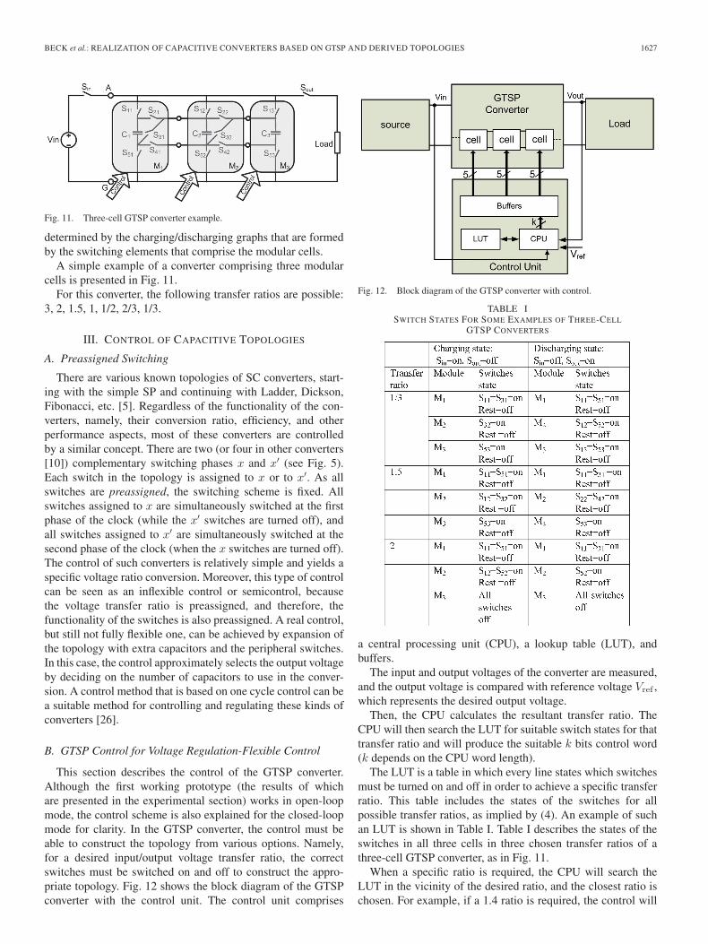
Fig. 11. Three-cell GTSP converter example.
determined by the charging/discharging graphs that are formedby the switching elements that comprise the modular cells.
A simple example of a converter comprising three modularcells is presented in Fig. 11.
For this converter, the following transfer ratios are possible:3, 2, 1.5, 1, 1/2, 2/3, 1/3.
III. CONTROL OF CAPACITIVE TOPOLOGIES
A. Preassigned Switching
There are various known topologies of SC converters, start-ing with the simple SP and continuing with Ladder, Dickson,Fibonacci, etc. [5]. Regardless of the functionality of the con-verters, namely, their conversion ratio, efficiency, and otherperformance aspects, most of these converters are controlledby a similar concept. There are two (or four in other converters[10]) complementary switching phases x and x′ (see Fig. 5).Each switch in the topology is assigned to x or to x′. As allswitches are preassigned, the switching scheme is fixed. Allswitches assigned to x are simultaneously switched at the firstphase of the clock (while the x′ switches are turned off), andall switches assigned to x′ are simultaneously switched at thesecond phase of the clock (when the x switches are turned off).The control of such converters is relatively simple and yields aspecific voltage ratio conversion. Moreover, this type of controlcan be seen as an inflexible control or semicontrol, becausethe voltage transfer ratio is preassigned, and therefore, thefunctionality of the switches is also preassigned. A real control,but still not fully flexible one, can be achieved by expansion ofthe topology with extra capacitors and the peripheral switches.In this case, the control approximately selects the output voltageby deciding on the number of capacitors to use in the conver-sion. A control method that is based on one cycle control can bea suitable method for controlling and regulating these kinds ofconverters [26].
B. GTSP Control for Voltage Regulation-Flexible Control
This section describes the control of the GTSP converter.Although the first working prototype (the results of whichare presented in the experimental section) works in open-loopmode, the control scheme is also explained for the closed-loopmode for clarity. In the GTSP converter, the control must beable to construct the topology from various options. Namely,for a desired input/output voltage transfer ratio, the correctswitches must be switched on and off to construct the appro-priate topology. Fig. 12 shows the block diagram of the GTSPconverter with the control unit. The control unit comprises
Fig. 12. Block diagram of the GTSP converter with control.
TABLE ISWITCH STATES FOR SOME EXAMPLES OF THREE-CELL
GTSP CONVERTERS
a central processing unit (CPU), a lookup table (LUT), andbuffers.
The input and output voltages of the converter are measured,and the output voltage is compared with reference voltage Vref ,which represents the desired output voltage.
Then, the CPU calculates the resultant transfer ratio. TheCPU will then search the LUT for suitable switch states for thattransfer ratio and will produce the suitable k bits control word(k depends on the CPU word length).
The LUT is a table in which every line states which switchesmust be turned on and off in order to achieve a specific transferratio. This table includes the states of the switches for allpossible transfer ratios, as implied by (4). An example of suchan LUT is shown in Table I. Table I describes the states of theswitches in all three cells in three chosen transfer ratios of athree-cell GTSP converter, as in Fig. 11.
When a specific ratio is required, the CPU will search theLUT in the vicinity of the desired ratio, and the closest ratio ischosen. For example, if a 1.4 ratio is required, the control will
1628 IEEE TRANSACTIONS ON INDUSTRIAL ELECTRONICS, VOL. 61, NO. 3, MARCH 2014
assign 1.5 because it is the closest to that desired. The decisionof the control will be to achieve accuracy and to minimizelosses, as will be explained in Section IV.
Note that there are other ways for creating the charging anddischarging graphs for a single transfer ratio. This implies thatthis converter has redundancy and that the switch schemes willbe chosen by an appropriate control.
Each cell requires data for controlling five switches, andthese data need to be synchronously received. Therefore, thelogic unit makes sure that the k-bit word of the CPU willbe stored in the buffers until all necessary data are readyfor all cells. Then, these data will be transferred to the cellssimultaneously.
IV. DYNAMIC LOSSES OF GTSP TOPOLOGY
Operation of capacitive-based converters implies losses dueto voltage drop on the capacitors, switching losses, conductionlosses, etc. These losses are discussed in detail in [5] and [27].In variable transfer ratio topologies, it is interesting to noteother kinds of losses that are the result of the variation of thetopology’s structure from one transfer ratio to another. GTSPtopology yields accurate output voltage or dc/dc voltage ratiosfor steady-state and slow variations. However, there are casesin which these kinds of converters might be developed forapplications other than power supplies, such as amplifiers or inthe case of power supplies when dealing with rare fast changesthat can occur due to voltage drops or fast load variations. Inthese cases, the dynamic limit of the topology can be estimatedby further study. GTSP has many dc/dc voltage ratios, andtherefore, by applying smart control, a specific desired voltagecan be attained.
Furthermore, the voltage can be achieved in various wayssince there is redundancy of transfer ratio values. This meansthat the control will enable for use those capacitors that willhave less voltage drop on them for faster dynamics. Thisprocedure will obviously be somewhat at the cost of accuracybecause voltage ratios that are close enough will be preferred.This will provide fewer losses rather than accuracy. Further-more, it may be possible to intelligently switch between thevarious configurations in order to minimize the dynamic powerlosses without affecting the output voltage regulation.
Next, the dynamics are demonstrated in terms of energy lossdue to the topology transition time from one voltage ratio toanother.
Assuming that the load is absorbing a constant power,the energy transferred to the load between two states of theconverter is
Wload = ΔT · Pload (6)
where ΔT is the time interval it takes the converter to stabilizeand stay when a transition from a given voltage transfer ratio toanother occurs.
For a single capacitor Ci, the energy loss in the case oftransition from state j to k is given by
ΔWi =1
2Ci
[v2ki − v2ji
](7)
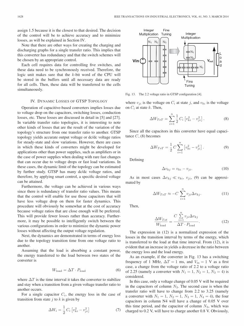
Fig. 13. The 2.2 voltage ratio in GTSP configuration [4].
where vji is the voltage on Ci at state j, and vki is the voltageon Ci at state k. Then,
ΔWToT =n∑
i=1
1
2Ci
[v2ki − v2ji
]. (8)
Since all the capacitors in this converter have equal capaci-tance C, (8) becomes
ΔWToT =1
2C
n∑i=1
[v2ki − v2ji
]. (9)
Defining
Δvkj = vki − vji. (10)
As in most cases Δvkj � vki, vji, (9) can be approxi-mated by
ΔWToT ≈ −C
n∑i=1
vjiΔvkj . (11)
Then,
ΔWTot
Wload=
Cn∑
i=1
vjiΔvkj
ΔT · Pload. (12)
The expression in (12) is a normalized expression of thelosses in the transition interval by terms of the energy, whichis transferred to the load at that time interval. From (12), it isevident that an increase in yields a decrease in the ratio betweenthe energy loss and the load energy.
As an example, if the converter in Fig. 13 has a switchingfrequency of 1 MHz, ΔT = 1 ms, and Vin = 1 V as a firstcase, a change from the voltage ratio of 2.2 to a voltage ratioof 2.25 (namely a converter with N1 = 1, N2 = 1, N3 = 4) isconsidered.
In this case, only a voltage change of 0.05 V will be requiredin the capacitors of column N3. The second case is when thetransfer ratio will have to change from 2.2 to 3.25 (namelya converter with N1 = 1, N2 = 1, N3 = 1, N4 = 4), the fourcapacitors in column N4 will have a change of 0.05 V overthis time period, and the capacitor of column N3, which wascharged to 0.2 V, will have to charge another 0.8 V. Obviously,
BECK et al.: REALIZATION OF CAPACITIVE CONVERTERS BASED ON GTSP AND DERIVED TOPOLOGIES 1629
case 2 will take more time to stabilize than case 1; however,in many applications in closed-loop converters, the changes inthe input voltage (or load change) are small, and the convertercompensates for a regulated output voltage. These cases areensured with faster dynamics, as shown in case 1.
Moreover, changes in load or in any other parameters thatrequire a shift in the operating conditions of the converters aremuch slower than the switching frequency, namely,
ΔT � Tswitching. (13)
The following measures can improve the dynamics of theconverter:
• increase in the switching frequency;• choosing the appropriate size of capacitors that will be
a compromise between minimizing switching losses andmaximizing the dynamics;
• minimize the ΔWTot by designing a control that choosesthe topology that will minimize the voltage drop of thecapacitors.
V. VOLTAGE DROP DUE TO OUTPUT RESISTANCE
For verification of the experimental results that will be intro-duced in the next section, a short discussion on output resistanceof SCs follows. There are numerous papers dealing with thecalculation of the output resistance of SC converters, such as[5] and [27]–[29]. In these works, several models for estimatingthe effective output resistance are presented. This resistanceimplies a voltage drop at the output of a loaded converter,which implies losses. This is the result of three mechanisms:1) capacitors’ ESR; 2) switches on resistance; and 3) a voltagedrop on the converter. This resistance can be written as
RO = RΔV +K1RESR +K2 ·Ron (14)
where K1 is a constant that reflects the structure of the topology.In the GTSP case, this constant is the voltage conversion ratioM of the circuit [17]. Namely, K1 = M.K2 is a constant thatmultiplies the on-resistance of the switches. This constant iscalculated by taking into account the total number of switchesthat are turned on with their respective connections at thespecified voltage ratio, and RΔV can be estimated in the caseof a 0.5 duty cycle of switching as [27]–[29]
RΔV =1
2 fCeq(15)
where f is the switching frequency, and Ceq is the equivalentcapacitance of the circuit at the discharging state. This capac-itance is calculated for a specific configuration of the GTSPconverter at the specific voltage transfer ratio.
Then, the voltage drop at the output can be calculated asfollows:
ΔVout = RO · VO
RL(16)
where VO is the measured output voltage, and RL is theresistance of the load.
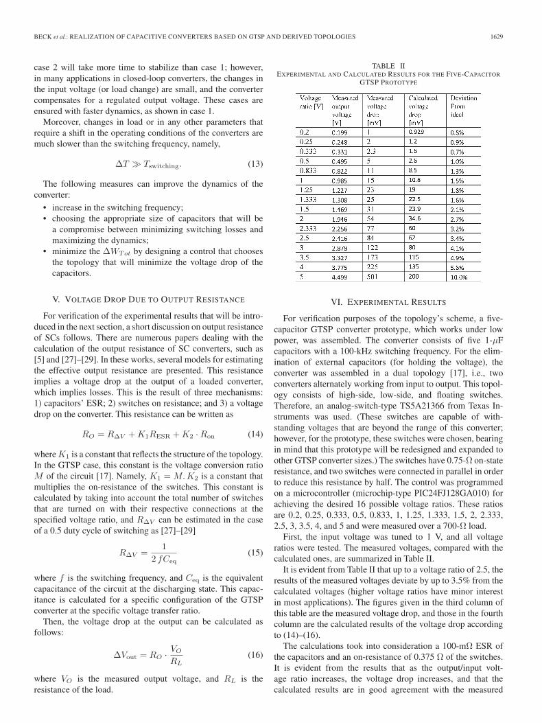
TABLE IIEXPERIMENTAL AND CALCULATED RESULTS FOR THE FIVE-CAPACITOR
GTSP PROTOTYPE
VI. EXPERIMENTAL RESULTS
For verification purposes of the topology’s scheme, a five-capacitor GTSP converter prototype, which works under lowpower, was assembled. The converter consists of five 1-μFcapacitors with a 100-kHz switching frequency. For the elim-ination of external capacitors (for holding the voltage), theconverter was assembled in a dual topology [17], i.e., twoconverters alternately working from input to output. This topol-ogy consists of high-side, low-side, and floating switches.Therefore, an analog-switch-type TS5A21366 from Texas In-struments was used. (These switches are capable of with-standing voltages that are beyond the range of this converter;however, for the prototype, these switches were chosen, bearingin mind that this prototype will be redesigned and expanded toother GTSP converter sizes.) The switches have 0.75-Ω on-stateresistance, and two switches were connected in parallel in orderto reduce this resistance by half. The control was programmedon a microcontroller (microchip-type PIC24FJ128GA010) forachieving the desired 16 possible voltage ratios. These ratiosare 0.2, 0.25, 0.333, 0.5, 0.833, 1, 1.25, 1.333, 1.5, 2, 2.333,2.5, 3, 3.5, 4, and 5 and were measured over a 700-Ω load.
First, the input voltage was tuned to 1 V, and all voltageratios were tested. The measured voltages, compared with thecalculated ones, are summarized in Table II.
It is evident from Table II that up to a voltage ratio of 2.5, theresults of the measured voltages deviate by up to 3.5% from thecalculated voltages (higher voltage ratios have minor interestin most applications). The figures given in the third column ofthis table are the measured voltage drop, and those in the fourthcolumn are the calculated results of the voltage drop accordingto (14)–(16).
The calculations took into consideration a 100-mΩ ESR ofthe capacitors and an on-resistance of 0.375 Ω of the switches.It is evident from the results that as the output/input volt-age ratio increases, the voltage drop increases, and that thecalculated results are in good agreement with the measured
1630 IEEE TRANSACTIONS ON INDUSTRIAL ELECTRONICS, VOL. 61, NO. 3, MARCH 2014
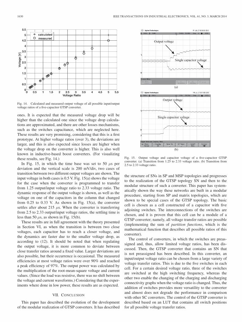
Fig. 14. Calculated and measured output voltage of all possible input/outputvoltage ratios of a five-capacitor GTSP converter.
ones. It is expected that the measured voltage drop will behigher than the calculated one since the voltage drop calcula-tions are approximated, and there are other losses mechanisms,such as the switches capacitance, which are neglected here.These results are very promising, considering that this is a firstprototype. At higher voltage ratios (over 3), the deviations arelarger, and this is also expected since losses are higher whenthe voltage drop on the converter is higher. This is also wellknown in inductive-based boost converters. (For visualizingthese results, see Fig. 14.)
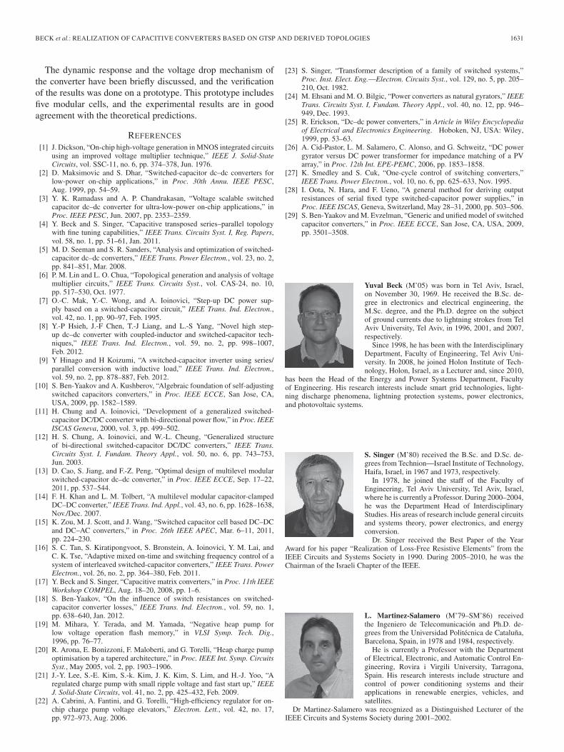
In Fig. 15, in which the time base was set to 50 μs perdeviation and the vertical scale is 200 mV/div, two cases oftransition between two different output voltages are shown. Theinput voltage in both cases is 0.5 V. Fig. 15(a) shows the voltagefor the case when the converter is programmed to transferfrom 1.25 output/input voltage ratio to 2.33 voltage ratio. Thedynamic response of the output voltage is shown, as well as thevoltage on one of the capacitors in the column that changedfrom 0.25 to 0.33 V. As shown in Fig. 15(a), the convertersettles after about 215 μs. When the converter is transferringfrom 2.5 to 2.33 output/input voltage ratios, the settling time isless than 50 μs, as shown in Fig. 15(b).
These results are in full agreement with the theory presentedin Section VI, as when the transition is between two closevoltages, each capacitor has to reach a closer voltage, andthe dynamics are faster due to the smaller voltage drop, asaccording to (12). It should be noted that when regulatingthe output voltage, it is more common to deviate betweenclose transfer ratios around a fixed value. Larger deviations arealso possible, but their occurrence is occasional. The measuredefficiencies at most voltage ratios were over 90% and reacheda peak efficiency of 97%. The output power was calculated bythe multiplication of the root-mean-square voltage and currentvalues. (Since the load was resistive, there was no shift betweenthe voltage and current waveforms.) Considering that the exper-iments where done in low power, these results are as expected.
VII. CONCLUSION
This paper has described the evolution of the developmentof the modular realization of GTSP converters. It has described
Fig. 15. Output voltage and capacitor voltage of a five-capacitor GTSPconverter. (a) Transition from 1.25 to 2.33 voltage ratio. (b) Transition from2.5 to 2.33 voltage ratio.
the structure of SNs in SP and MSP topologies and progressesto the realization of the GTSP topology SN and then to themodular structure of such a converter. This paper has system-atically shown the way these networks are built in a modularprocedure, starting from SP and matrix topologies, which areshown to be special cases of the GTSP topology. The basiccell is chosen as a cell constructed of a capacitor with fiveadjoining switches. The interconnections of the switches arechosen, and it is proven that this cell can be a module of aGTSP converter; namely, all voltage transfer ratios are possible(implementing the sum of partition functions, which is themathematical function that describes all possible ratios of thisconverter).
The control of converters, in which the switches are preas-signed and, thus, allow limited voltage ratios, has been dis-cussed. Then, the GTSP converter that contains an SN thatis not preassigned has been described. In this converter, aninput/output voltage ratio can be chosen from a large variety ofvoltage transfer ratios. This is due to the five switches in eachcell. For a certain desired voltage ratio, three of the switchesare switched at the high switching frequency, whereas theother two enable the changing of the charging and dischargingconnectivity graphs when the voltage ratio is changed. Thus, theaddition of switches provides more versatility to the converterand almost does not degrade the performance in comparisonwith other SC converters. The control of the GTSP converter isdescribed based on an LUT that contains all switch positionsfor all possible voltage transfer ratios.
BECK et al.: REALIZATION OF CAPACITIVE CONVERTERS BASED ON GTSP AND DERIVED TOPOLOGIES 1631
The dynamic response and the voltage drop mechanism ofthe converter have been briefly discussed, and the verificationof the results was done on a prototype. This prototype includesfive modular cells, and the experimental results are in goodagreement with the theoretical predictions.
REFERENCES
[1] J. Dickson, “On-chip high-voltage generation in MNOS integrated circuitsusing an improved voltage multiplier technique,” IEEE J. Solid-StateCircuits, vol. SSC-11, no. 6, pp. 374–378, Jun. 1976.
[2] D. Maksimovic and S. Dhar, “Switched-capacitor dc–dc converters forlow-power on-chip applications,” in Proc. 30th Annu. IEEE PESC,Aug. 1999, pp. 54–59.
[3] Y. K. Ramadass and A. P. Chandrakasan, “Voltage scalable switchedcapacitor dc–dc converter for ultra-low-power on-chip applications,” inProc. IEEE PESC, Jun. 2007, pp. 2353–2359.
[4] Y. Beck and S. Singer, “Capacitive transposed series–parallel topologywith fine tuning capabilities,” IEEE Trans. Circuits Syst. I, Reg. Papers,vol. 58, no. 1, pp. 51–61, Jan. 2011.
[5] M. D. Seeman and S. R. Sanders, “Analysis and optimization of switched-capacitor dc–dc converters,” IEEE Trans. Power Electron., vol. 23, no. 2,pp. 841–851, Mar. 2008.
[6] P. M. Lin and L. O. Chua, “Topological generation and analysis of voltagemultiplier circuits,” IEEE Trans. Circuits Syst., vol. CAS-24, no. 10,pp. 517–530, Oct. 1977.
[7] O.-C. Mak, Y.-C. Wong, and A. Ioinovici, “Step-up DC power sup-ply based on a switched-capacitor circuit,” IEEE Trans. Ind. Electron.,vol. 42, no. 1, pp. 90–97, Feb. 1995.
[8] Y.-P Hsieh, J.-F Chen, T.-J Liang, and L.-S Yang, “Novel high step-up dc–dc converter with coupled-inductor and switched-capacitor tech-niques,” IEEE Trans. Ind. Electron., vol. 59, no. 2, pp. 998–1007,Feb. 2012.
[9] Y Hinago and H Koizumi, “A switched-capacitor inverter using series/parallel conversion with inductive load,” IEEE Trans. Ind. Electron.,vol. 59, no. 2, pp. 878–887, Feb. 2012.
[10] S. Ben-Yaakov and A. Kushberov, “Algebraic foundation of self-adjustingswitched capacitors converters,” in Proc. IEEE ECCE, San Jose, CA,USA, 2009, pp. 1582–1589.
[11] H. Chung and A. Ioinovici, “Development of a generalized switched-capacitor DC/DC converter with bi-directional power flow,” in Proc. IEEEISCAS Geneva, 2000, vol. 3, pp. 499–502.
[12] H. S. Chung, A. Ioinovici, and W.-L. Cheung, “Generalized structureof bi-directional switched-capacitor DC/DC converters,” IEEE Trans.Circuits Syst. I, Fundam. Theory Appl., vol. 50, no. 6, pp. 743–753,Jun. 2003.
[13] D. Cao, S. Jiang, and F.-Z. Peng, “Optimal design of multilevel modularswitched-capacitor dc–dc converter,” in Proc. IEEE ECCE, Sep. 17–22,2011, pp. 537–544.
[14] F. H. Khan and L. M. Tolbert, “A multilevel modular capacitor-clampedDC–DC converter,” IEEE Trans. Ind. Appl., vol. 43, no. 6, pp. 1628–1638,Nov./Dec. 2007.
[15] K. Zou, M. J. Scott, and J. Wang, “Switched capacitor cell based DC–DCand DC–AC converters,” in Proc. 26th IEEE APEC, Mar. 6–11, 2011,pp. 224–230.
[16] S. C. Tan, S. Kiratipongvoot, S. Bronstein, A. Ioinovici, Y. M. Lai, andC. K. Tse, “Adaptive mixed on-time and switching frequency control of asystem of interleaved switched-capacitor converters,” IEEE Trans. PowerElectron., vol. 26, no. 2, pp. 364–380, Feb. 2011.
[17] Y. Beck and S. Singer, “Capacitive matrix converters,” in Proc. 11th IEEEWorkshop COMPEL, Aug. 18–20, 2008, pp. 1–6.
[18] S. Ben-Yaakov, “On the influence of switch resistances on switched-capacitor converter losses,” IEEE Trans. Ind. Electron., vol. 59, no. 1,pp. 638–640, Jan. 2012.
[19] M. Mihara, Y. Terada, and M. Yamada, “Negative heap pump forlow voltage operation flash memory,” in VLSI Symp. Tech. Dig.,1996, pp. 76–77.
[20] R. Arona, E. Bonizzoni, F. Maloberti, and G. Torelli, “Heap charge pumpoptimisation by a tapered architecture,” in Proc. IEEE Int. Symp. CircuitsSyst., May 2005, vol. 2, pp. 1903–1906.
[21] J.-Y. Lee, S.-E. Kim, S.-k. Kim, J. K. Kim, S. Lim, and H.-J. Yoo, “Aregulated charge pump with small ripple voltage and fast start up,” IEEEJ. Solid-State Circuits, vol. 41, no. 2, pp. 425–432, Feb. 2009.
[22] A. Cabrini, A. Fantini, and G. Torelli, “High-efficiency regulator for on-chip charge pump voltage elevators,” Electron. Lett., vol. 42, no. 17,pp. 972–973, Aug. 2006.
[23] S. Singer, “Transformer description of a family of switched systems,”Proc. Inst. Elect. Eng.––Electron. Circuits Syst., vol. 129, no. 5, pp. 205–210, Oct. 1982.
[24] M. Ehsani and M. O. Bilgic, “Power converters as natural gyrators,” IEEETrans. Circuits Syst. I, Fundam. Theory Appl., vol. 40, no. 12, pp. 946–949, Dec. 1993.
[25] R. Erickson, “Dc–dc power converters,” in Article in Wiley Encyclopediaof Electrical and Electronics Engineering. Hoboken, NJ, USA: Wiley,1999, pp. 53–63.
[26] A. Cid-Pastor, L. M. Salamero, C. Alonso, and G. Schweitz, “DC powergyrator versus DC power transformer for impedance matching of a PVarray,” in Proc. 12th Int. EPE-PEMC, 2006, pp. 1853–1858.
[27] K. Smedley and S. Cuk, “One-cycle control of switching converters,”IEEE Trans. Power Electron., vol. 10, no. 6, pp. 625–633, Nov. 1995.
[28] I. Oota, N. Hara, and F. Ueno, “A general method for deriving outputresistances of serial fixed type switched-capacitor power supplies,” inProc. IEEE ISCAS, Geneva, Switzerland, May 28–31, 2000, pp. 503–506.
[29] S. Ben-Yaakov and M. Evzelman, “Generic and unified model of switchedcapacitor converters,” in Proc. IEEE ECCE, San Jose, CA, USA, 2009,pp. 3501–3508.
Yuval Beck (M’05) was born in Tel Aviv, Israel,on November 30, 1969. He received the B.Sc. de-gree in electronics and electrical engineering, theM.Sc. degree, and the Ph.D. degree on the subjectof ground currents due to lightning strokes from TelAviv University, Tel Aviv, in 1996, 2001, and 2007,respectively.
Since 1998, he has been with the InterdisciplinaryDepartment, Faculty of Engineering, Tel Aviv Uni-versity. In 2008, he joined Holon Institute of Tech-nology, Holon, Israel, as a Lecturer and, since 2010,
has been the Head of the Energy and Power Systems Department, Facultyof Engineering. His research interests include smart grid technologies, light-ning discharge phenomena, lightning protection systems, power electronics,and photovoltaic systems.
S. Singer (M’80) received the B.Sc. and D.Sc. de-grees from Technion—Israel Institute of Technology,Haifa, Israel, in 1967 and 1973, respectively.
In 1978, he joined the staff of the Faculty ofEngineering, Tel Aviv University, Tel Aviv, Israel,where he is currently a Professor. During 2000–2004,he was the Department Head of InterdisciplinaryStudies. His areas of research include general circuitsand systems theory, power electronics, and energyconversion.
Dr. Singer received the Best Paper of the YearAward for his paper “Realization of Loss-Free Resistive Elements” from theIEEE Circuits and Systems Society in 1990. During 2005–2010, he was theChairman of the Israeli Chapter of the IEEE.
L. Martinez-Salamero (M’79–SM’86) receivedthe Ingeniero de Telecomunicación and Ph.D. de-grees from the Universidad Politécnica de Cataluña,Barcelona, Spain, in 1978 and 1984, respectively.
He is currently a Professor with the Departmentof Electrical, Electronic, and Automatic Control En-gineering, Rovira i Virgili University, Tarragona,Spain. His research interests include structure andcontrol of power conditioning systems and theirapplications in renewable energies, vehicles, andsatellites.
Dr Martinez-Salamero was recognized as a Distinguished Lecturer of theIEEE Circuits and Systems Society during 2001–2002.
Related Documents