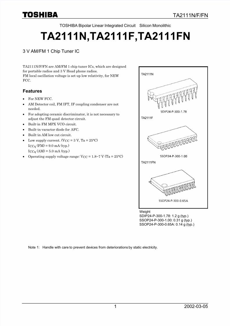
TA2111N/F/FN 2002-03-05 1 TOSHIBA Bipolar Linear Integrated Circuit Silicon Monolithic TA2111N,TA2111F,TA2111FN 3 V AM/FM 1 Chip Tuner IC TA2111N/F/FN are AM/FM 1 chip tuner ICs, which are designed for portable radios and 3 V Head phone radios. FM local oscillation voltage is set up low relativity, for NEW FCC. Features · For NEW FCC. · AM Detector coil, FM IFT, IF coupling condenser are not needed. · For adopting ceramic discriminator, it is not necessary to adjust the FM quad detector circuit. · Built-in FM MPX VCO circuit. · Built-in varactor diode for AFC. · Built-in AM low cut circuit. · Low supply current. (VCC = 3 V, Ta = 25°C) I CCq (FM) = 9.0 mA (typ.) ICCq (AM) = 5.0 mA (typ.) · Operating supply voltage range: V CC = 1.8~7 V (Ta = 25°C) Note 1: Handle with care to prevent dev ices from deteriorations by static electricity. TA2111N TA2111F TA2111FN Weight SDIP24-P-300-1.78: 1.2 g (typ.) SSOP24-P-300-1.00: 0.31 g (typ.) SSOP24-P-300-0.65A: 0.14 g (typ.)

Welcome message from author
This document is posted to help you gain knowledge. Please leave a comment to let me know what you think about it! Share it to your friends and learn new things together.
Transcript
8/7/2019 MODULADOR AM TOSHIBA
http://slidepdf.com/reader/full/modulador-am-toshiba 1/18
TA2111N/F/FN
TOSHIBA Bipolar Linear Integrated Circuit Silicon Monolithic
TA2111N,TA2111F,TA2111FN
3 V AM/FM 1 Chip Tuner IC
TA2111N/F/FN are AM/FM 1 chip tuner ICs, which are designed
for portable radios and 3 V Head phone radios.
FM local oscillation voltage is set up low relativity, for NEW
FCC.
Features
· For NEW FCC.
· AM Detector coil, FM IFT, IF coupling condenser are not
needed.
· For adopting ceramic discriminator, it is not necessary toadjust the FM quad detector circuit.
· Built-in FM MPX VCO circuit.
· Built-in varactor diode for AFC.
· Built-in AM low cut circuit.
· Low supply current. (VCC = 3 V, Ta = 25°C)
ICCq (FM) = 9.0 mA (typ.)
ICCq (AM) = 5.0 mA (typ.)
· Operating supply voltage range: VCC = 1.8~7 V (Ta = 25°C)
Note 1: Handle with care to prevent devices from deteriorations by static electricity.
TA2111N
TA2111F
TA2111FN
Weight
SDIP24-P-300-1.78: 1.2 g (typ.)
SSOP24-P-300-1.00: 0.31 g (typ.)
SSOP24-P-300-0.65A: 0.14 g (typ.)
8/7/2019 MODULADOR AM TOSHIBA
http://slidepdf.com/reader/full/modulador-am-toshiba 2/18
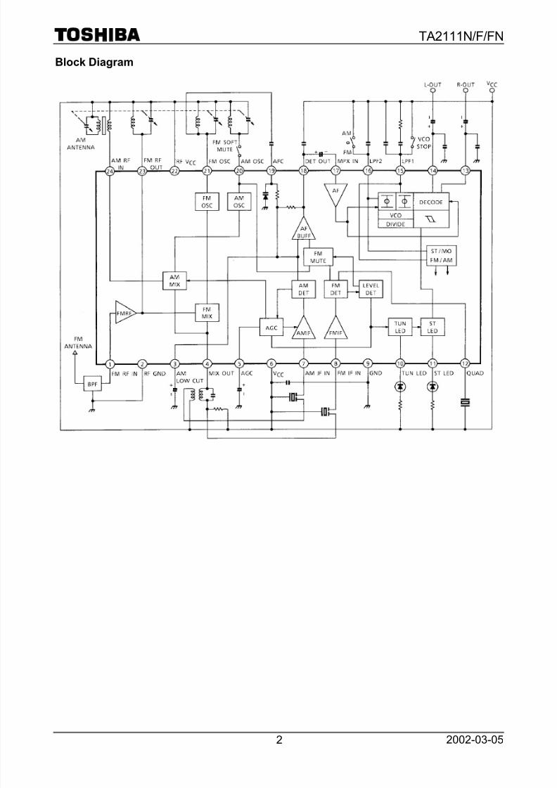
TA2111N/F/FN
Block Diagram

8/7/2019 MODULADOR AM TOSHIBA
http://slidepdf.com/reader/full/modulador-am-toshiba 3/18
TA2111N/F/FN
Explanation of Terminals(Terminal voltage: Typical terminal voltage at no signal with test circuit, VCC = 3 V,Ta = 25°C)
Terminal Voltage
(Typ.) (V)Pin
No.Characteristics Internal Circuit
AM FM
1 FM-RF IN 0 0.8
2RF GND (GND for FM RF,FM OSC stage)
― 0 0
3 AM LOW CUT 1.0 0.8
4 MIX OUT 3.0 2.9
5 AGC (AM AGC) 0 0
6VCC (VCC for AM, FM IF,FM MPX stage)
― 3.0 3.0
7 AM IF IN 2.3 2.6

8/7/2019 MODULADOR AM TOSHIBA
http://slidepdf.com/reader/full/modulador-am-toshiba 4/18
TA2111N/F/FN
Terminal Voltage
(Typ.) (V)Pin
No.Characteristics Internal Circuit
AM FM
8 FM IF IN 3.0 3.0
9GND (GND for AM, FM IF,FM MPX stage)
― 0 0
10 TUN LED (Tuning LED) ― ―
11 ST LED (Stereo LED) ― ―
12QUAD(FM QUAD. Detector)
2.5 2.2
1314
R-OUT (R-ch Output)L-OUT (L-ch Output)
1.2 1.2
8/7/2019 MODULADOR AM TOSHIBA
http://slidepdf.com/reader/full/modulador-am-toshiba 5/18
TA2111N/F/FN
Terminal Voltage
(Typ.) (V)Pin
No.Characteristics Internal Circuit
AM FM
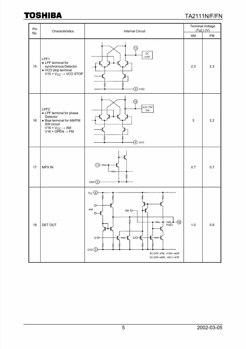
15
LPF1 LPF terminal for
synchronous Detector VCO stop terminal
V15 = VCC → VCO STOP
2.3 2.3
16
LPF2 LPF terminal for phase
Detector Bias terminal for AM/FM
SW circuitV16 = VCC → AMV16 = OPEN → FM
3 2.2
17 MPX IN 0.7 0.7
18 DET OUT 1.0 0.9

8/7/2019 MODULADOR AM TOSHIBA
http://slidepdf.com/reader/full/modulador-am-toshiba 6/18
TA2111N/F/FN
Terminal Voltage
(Typ.) (V)Pin
No.Characteristics Internal Circuit
AM FM
19 AFC cf. pin 3 ― ―
20 AM OSC 3.0 3.0
21 FM OSC 3.0 3.0
22RF VCC (VCC for FM OSC stage)
― 3.0 3.0
23 FM RF OUT cf. pin 1 3.0 3.0
24 AM RF IN 3.0 3.0

8/7/2019 MODULADOR AM TOSHIBA
http://slidepdf.com/reader/full/modulador-am-toshiba 7/18
TA2111N/F/FN
Application Note
1. AM low-cut circuit
· The AM Low-Cut action is carried out by the bypass of the high frequency
component of the positive-feedback signal at the AF AMP stage.
The external capacitor: C3 by-passes this component.
· The cut-off frequency f L
is determined by the internal resistance 10 kΩ
(typ.) and the external capacitor C3 as following ;
· In the case of the AM Low-Cut function is not needed, set up the value of C3 over 1 µF. In the condition
of C3 ≥ 1 µF, the frequency characteristic has flat response at the low frequency.
· In FM mode, C3 is a capacitor for AFC Low-Pass filter circuit.
2. FM detection circuit
For the FM detection circuit, detection coil is able to use instead of ceramic discriminator. Recommended
circuit and recommended coil are as follows. In this case, please take care that Vin (lim.) falls a little.
TurnsTest Frequency
Co
(pF)Qo
1-2 2-3 1-3 4-6
Wire
(mmφ)Reference
10.7 MHz 51 45 ― ― 30 ― 0.08 UEWTOKO Co., Ltd.
600BEAS-10018Z
Maximum Ratings (Ta = 25°C)
Characteristics Symbol Rating Unit
Supply voltage VCC 8 V
LED current ILED 10 mA
LED voltage VLED 8 V
TA2111N 1200
TA2111F 400Power dissipation
TA2111FN
PD (Note 2)
500
mW
Operating temperature Topr −25~75 °C
Storage temperature Tstg −55~150 °C
Note 2: Derated above Ta = 25°C in the proportion of 9.6 mW/°C for TA2111N, of 3.2 mW/°C for TA2111F and of
4 mW/°C for TA2111FN.

8/7/2019 MODULADOR AM TOSHIBA
http://slidepdf.com/reader/full/modulador-am-toshiba 8/18
TA2111N/F/FN
Electrical Characteristicsunless otherwise specified, Ta = 25°C, VCC = 3 V,
F/E : f = 98 MHz, f m = 1 kHzFM IF : f = 10.7 MHz,∆f = ±22.5 kHz, f m = 1 kHzAM : f = 1 MHz, MOD = 30%, f m = 1 kHzMPX : f m = 1 kHz
Characteristics Symbol TestCircuit
Test Condition Min Typ. Max Unit
ICC (FM) 1 Vin = 0, FM mode ― 9 12.5Supply current
ICC (AM) 1 Vin = 0, AM mode ― 5 7.5mA
Input limiting voltage Vin (lim) 1 −3dB limiting ― 7 ― dBµVEMFF/E
Local OSC voltage VOSC 2 f OSC = 108.7 MHz ― 105 ― mVrms
Input limiting voltage Vin (l im) IF 1 −3dB limiting 35 40 45dBµVEMF
Recovered output voltage VOD 1 Vin = 80dBµV EMF 60 75 90 mVrms
Signal to noise ratio S/N 1 Vin = 80dBµV EMF ― 65 ― dB
Total harmonic distortion THD 1 Vin = 80dBµV EMF ― 0.2 ― %
AM rejection ration AMR 1 Vin = 80dBµV EMF ― 45 ― dB
LED on sensitivity VL 1 IL = 1 mA 40 45 50dBµVEMF
FMIF
Soft mute attenuation MUTE 1 Vin = 0 ― 20 ― dB
Gain GV 1 Vin = 25dBµV EMF 18 35 70 mVrms
Recovered output voltage VOD 1 Vin = 60dBµV EMF 50 70 90 mVrms
Signal to noise ratio S/N 1 Vin = 60dBµV EMF ― 41 ― dB
Total harmonic distortion THD 1 Vin = 60dBµV EMF ― 0.7 ― %
AM
LED on sensitivity VL 1 IL = 1 mA 23 28 33
dBµV
EMF
FM mode ― 0.75 ― Pin 18 output resistance R18 ―
AM mode ― 15.5 ― kΩ
Input resistance RIN ― ― ― 55 ― kΩ
Output resistance ROUT ― ― ― 5 ― kΩ
Max composite signal inputvoltage
Vin MAX(STEREO)
1L + R = 90%, P = 10%,f m = 1 kHz, THD = 3%
― 700 ― mVrms
f m = 100 Hz ― 45 ―
f m = 1 kHz 45 ― Separation Sep 1L + R =180 mVrms,P = 20 mVrms
f m = 10 kHz ― 45 ―
dB
MonauralTHD
(MONAURAL)1 Vin = 200 mVrms ― 0.3 ―
Total harmonicdistortion
StereoTHD
(STEREO)1
L + R = 180 mVrms,P = 20 mVrms
― 0.3 ―
%
Voltage gain GV 1 Vin = 200 mVrms −2.5 −1 0.5 dB
Channel balance C.B. 1 Vin = 200 mVrms −1.5 0 1.5 dB
ON VL (ON) 1 ― 8 12Stereo LEDsensitivity OFF VL (OFF) 1
Pilot input3 6 ―
mVrms
Stereo LED hysteresis VH 1To LED turn off from LED turnon
― 2 ― mVrms
Capture range C.R. 1 P = 20 mVrms ― ±8 ― %
MPX
Signal to noise ratio S/N 1 ― ― 80 ― dB

8/7/2019 MODULADOR AM TOSHIBA
http://slidepdf.com/reader/full/modulador-am-toshiba 9/18
TA2111N/F/FN
Test Circuit 1

8/7/2019 MODULADOR AM TOSHIBA
http://slidepdf.com/reader/full/modulador-am-toshiba 10/18
TA2111N/F/FN
Test Circuit 2
Coil Data
TurnsCoil No. Test Freq.
L
(µH)
Co
(pF)Qo
1-2 2-3 1-3 1-4 4-6
Wire
(mmφ)Reference
L1 FM RF 100 MHz ― ― 79 ― ― ― 2
12 ― 0.16UEW
TOKO Co., Ltd.666SNF-305NK
L2 FM OSC 100 MHz ― ― 76 ― ― ― 2 ― 0.16UEWTOKO Co., Ltd.666SNF-306NK
T1 AM OSC 796 kHz 268 ― 65 19 95 ― ― ― 0.05UEWTOKO Co., Ltd.5PNR-5146Y
T2 AM IFT 455 kHz ― 470 60 ― ― 109 ― 7 0.05UEW TOKO Co., Ltd.5PLG-5147X
8/7/2019 MODULADOR AM TOSHIBA
http://slidepdf.com/reader/full/modulador-am-toshiba 11/18
TA2111N/F/FN
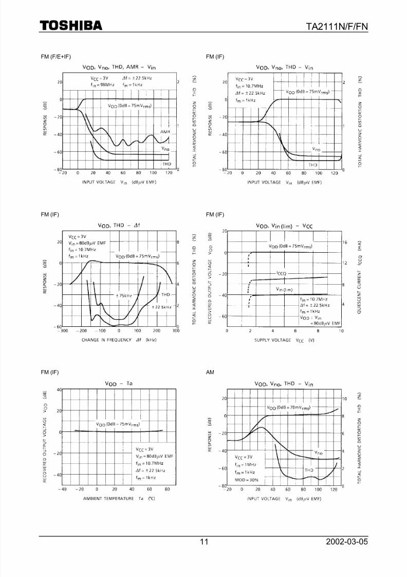
FM (F/E+IF) FM (IF)
FM (IF) FM (IF)
FM (IF) AM

8/7/2019 MODULADOR AM TOSHIBA
http://slidepdf.com/reader/full/modulador-am-toshiba 12/18
TA2111N/F/FN
AM AM
AM MPX
MPX MPX

8/7/2019 MODULADOR AM TOSHIBA
http://slidepdf.com/reader/full/modulador-am-toshiba 13/18
TA2111N/F/FN
MPX MPX
MPX
8/7/2019 MODULADOR AM TOSHIBA
http://slidepdf.com/reader/full/modulador-am-toshiba 14/18
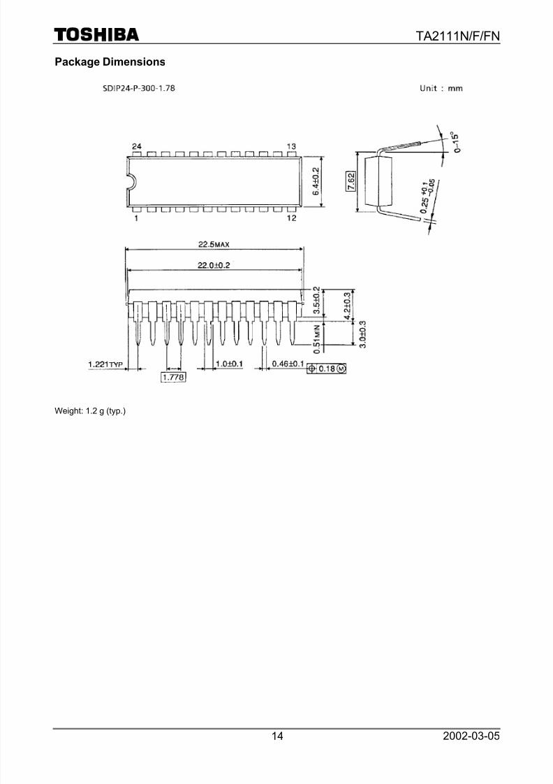
TA2111N/F/FN
Package Dimensions
Weight: 1.2 g (typ.)

8/7/2019 MODULADOR AM TOSHIBA
http://slidepdf.com/reader/full/modulador-am-toshiba 15/18
8/7/2019 MODULADOR AM TOSHIBA
http://slidepdf.com/reader/full/modulador-am-toshiba 16/18
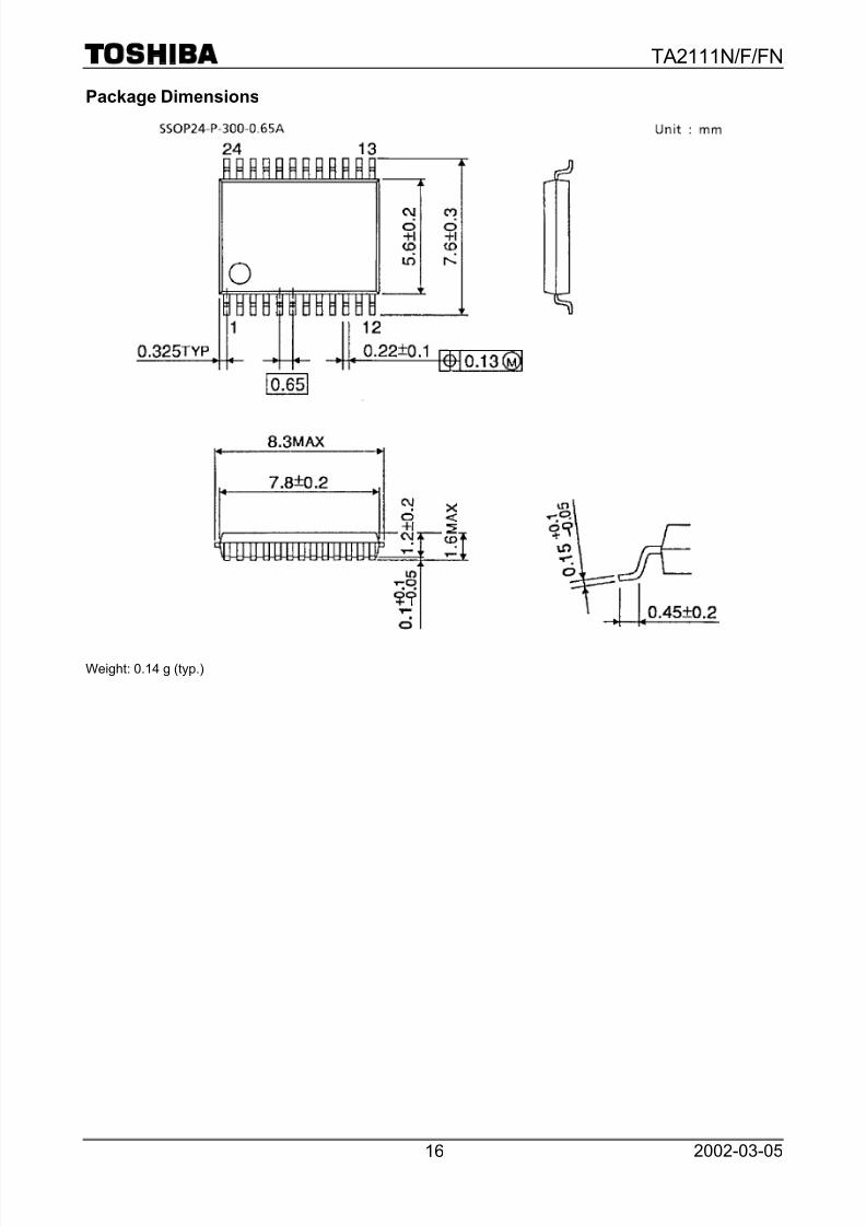
TA2111N/F/FN
Package Dimensions
Weight: 0.14 g (typ.)

8/7/2019 MODULADOR AM TOSHIBA
http://slidepdf.com/reader/full/modulador-am-toshiba 17/18
TA2111N/F/FN
· TOSHIBA is continually working to improve the quality and reliability of its products. Nevertheless, semiconductor
devices in general can malfunction or fail due to their inherent electrical sensitivity and vulnerability to physical
stress. It is the responsibility of the buyer, when utilizing TOSHIBA products, to comply with the standards of
safety in making a safe design for the entire system, and to avoid situations in which a malfunction or failure of
such TOSHIBA products could cause loss of human life, bodily injury or damage to property.
In developing your designs, please ensure that TOSHIBA products are used within specified operating ranges as
set forth in the most recent TOSHIBA products specifications. Also, please keep in mind the precautions and
conditions set forth in the “Handling Guide for Semiconductor Devices,” or “TOSHIBA Semiconductor Reliability
Handbook” etc..
· The TOSHIBA products listed in this document are intended for usage in general electronics applications
(computer, personal equipment, office equipment, measuring equipment, industrial robotics, domestic appliances,
etc.). These TOSHIBA products are neither intended nor warranted for usage in equipment that requiresextraordinarily high quality and/or reliability or a malfunction or failure of which may cause loss of human life or
bodily injury (“Unintended Usage”). Unintended Usage include atomic energy control instruments, airplane or
spaceship instruments, transportation instruments, traffic signal instruments, combustion control instruments,
medical instruments, all types of safety devices, etc.. Unintended Usage of TOSHIBA products listed in this
document shall be made at the customer’s own risk.
· The products described in this document are subject to the foreign exchange and foreign trade laws.
· The information contained herein is presented only as a guide for the applications of our products. No
responsibility is assumed by TOSHIBA CORPORATION for any infringements of intellectual property or other
rights of the third parties which may result from its use. No license is granted by implication or otherwise under
any intellectual property or other rights of TOSHIBA CORPORATION or others.
· The information contained herein is subject to change without notice.
000707EBARESTRICTIONS ON PRODUCT USE

8/7/2019 MODULADOR AM TOSHIBA
http://slidepdf.com/reader/full/modulador-am-toshiba 18/18
This datasheet has been download from:
www.datasheetcatalog.com
Datasheets for electronics components.
Related Documents