UNIVERSITY OF SOUTHAMPTON Modified Chalcogenide Glasses for Optical Device Applications by Mark A. Hughes A thesis submitted for the degree of Doctor of Philosophy Faculty of Engineering, Science & Mathematics Optoelectronics Research Centre May 2007

Welcome message from author
This document is posted to help you gain knowledge. Please leave a comment to let me know what you think about it! Share it to your friends and learn new things together.
Transcript
UNIVERSITY OF SOUTHAMPTON
Modified Chalcogenide Glasses for Optical Device Applications
by
Mark A. Hughes
A thesis submitted for the degree of Doctor of Philosophy
Faculty of Engineering, Science & Mathematics Optoelectronics Research Centre
May 2007
UNIVERSITY OF SOUTHAMPTON
ABSTRACT
FACULTY OF ENGINEERING, SCIENCE & MATHEMATICS OPTOELECTRONICS RESEARCH CENTRE
Doctor of Philosophy
MODIFIED CHALCOGENIDE GLASSES FOR OPTICAL DEVICE
APPLICATIONS
by Mark A. Hughes This thesis focuses on two different, but complementary, aspects of the modification of gallium lanthanum sulphide (GLS) glasses. Firstly the addition of transition metal ions as dopants is examined and their potential for use as active optical materials is explored. It is also argued that the spectroscopic analysis of transition metal ions is a useful tool for evaluating the local environment of their host. Secondly femtosecond (fs) laser modification of GLS is investigated as a method for waveguide formation. Vanadium doped GLS displays three absorption bands at 580, 730 and 1155 nm identified by photoluminescence excitation measurements. Broad photoluminescence, with a full width half maximum of ~500 nm, is observed peaking at 1500 nm when exciting at 514, 808 and 1064 nm. The fluorescence lifetime and quantum efficiency at 300 K were measured to be 33.4 µs and 4% respectively. Analysis of the emission decay, at various vanadium concentrations, indicated a preferentially filled, high efficiency, oxide site that gives rise to characteristic long lifetimes and a low efficiency sulphide site that gives rise to characteristic short lifetimes. X-ray photoelectron spectroscopy measurements indicated the presence of vanadium in a broad range of oxidation states from V+ to V5+. Tanabe-Sugano analysis indicates that the optically active ion is V2+ in octahedral coordination and the crystal field strength (Dq/B) was 1.84. Titanium and nickel doped GLS display a single absorption band at 590 and 690 nm, and emission lifetimes of 97 and 70 µs respectively. Bismuth doped GLS displays two absorption bands at 665 and 850 nm and lifetime components of 7 and 47 µs. Based on comparisons to other work the optically active ions are proposed to be Ti3+, Ni+ and Bi+, all of these displayed emission peaking at ~900 nm. Through optical characterisation of fs laser written waveguides in GLS, a formation mechanism has been proposed. Tunnelling has been identified as the dominant nonlinear absorption mechanism in the formation of the waveguides. Single mode guidance at 633 nm has been demonstrated. The writing parameters for the minimum propagation loss of 1.47 dB/cm are 0.36 µJ pulse energy and 50 µm/s scanning speed. The observation of spectral broadening in these waveguides indicates that they may have applications for nonlinear optical devices. Fs laser written waveguides in transition metal doped GLS could lead to broadband active optical devices.
i
Contents Nomenclature . . . . . . . . v List of figures . . . . . . . . . vii List of tables . . . . . . . . . xii Acknowledgements . . . . . . . . xv 1 Introduction . . . . . . . . 1
1.1 Motivation . . . . . . . . 1 1.2 Gallium lanthanum sulphide (GLS) glass . . . . 3 1.3 Transition metal dopants . . . . . . 4 1.4 Waveguide technology. . . . . . . 5 1.5 Scope of the thesis. . . . . . . . 6
2 Background . . . . . . . . 8
2.1 Introduction . . . . . . . . 8 2.2 Spectroscopy basics . . . . . . . 8
2.2.1 Absorption measurements . . . . . 8 2.2.2 Excited state absorption . . . . . 8 2.2.3 Lifetime measurements . . . . . . 9
2.3 Crystal field theory . . . . . . . 9 2.4 Group theory . . . . . . . . 14 2.5 The single configurational coordinate model . . . . 15 2.6 Broadening mechanisms . . . . . . 18
2.6.1 Homogeneous broadening . . . . . 18 2.6.2 Inhomogeneous broadening . . . . . 18
2.7 Selection rules . . . . . . . 19 2.8 Structure of GLS . . . . . . . 19
2.8.1 General structure of glass . . . . . 19 2.8.2 Chalcogenide glass . . . . . . 20 2.8.3 GLS glass . . . . . . . 20
3 Glass melting and spectroscopic techniques . . . . 22
3.1 Introduction . . . . . . . . 22 3.2 Glass melting procedures . . . . . . 22
3.2.1 Batching and melting details of transition metal doped GLS samples 22 3.2.2 Batching and melting details of vanadium doped GLS samples 24
3.3 Spectroscopic techniques . . . . . . 26 3.3.1 Absorption spectroscopy . . . . . 26 3.3.2 Photoluminescence spectroscopy . . . . 27 3.3.3 Photoluminescence Excitation Spectroscopy . . . 30 3.3.4 Temporally resolved fluorescence lifetime . . . 34 3.3.5 Frequency resolved fluorescence lifetime . . . 35 3.3.6 Raman spectroscopy . . . . . . 36 3.3.7 Quantum efficiency . . . . . . 37 3.3.8 X-ray Photoelectron Spectroscopy . . . . 39
ii
3.3.9 Electron paramagnetic resonance . . . . 41 3.3.10 Summary of spectroscopic techniques . . . . 44
4 Vanadium doped chalcogenide glass . . . . . 45
4.1 Introduction . . . . . . . . 45 4.2 Absorption measurements . . . . . . 46 4.3 Derivative absorption spectroscopy . . . . . 50 4.4 Photoluminescence of vanadium doped GLS . . . . 54
4.4.1 Photoluminescence spectra . . . . . 54 4.4.2 Discussion of photoluminescence spectra . . . 58
4.5 Photoluminescence excitation of vanadium doped GLS . . 60 4.6 Fluorescence Lifetime . . . . . . 63
4.6.1 Introduction to the stretched exponential function . . 63 4.6.2 Experimental and analysis techniques . . . . 64
4.7 Time resolved fluorescence decay data for vanadium doped GLS . 65 4.8 Average Lifetime . . . . . . . 72 4.9 Frequency resolved lifetime measurements of vanadium doped GLS 74 4.10 Continuous lifetime distribution analysis of vanadium doped GLS 76 4.11 Temperature dependence of emission lifetime . . . 81
4.11.1 Introduction . . . . . . . 81 4.11.2 Determination of quantum efficiency . . . . 81 4.11.3 Struck- Fonger fit . . . . . . 81 4.11.4 Parameter estimation . . . . . . 82 4.11.5 Temperature dependent lifetime measurements . . 84
4.12 Quantum efficiency measurements . . . . . 87 4.13 X-ray Photoelectron Spectroscopy . . . . . 90 4.14 Electron paramagnetic resonance . . . . . 92 4.15 Determination of the oxidation state and coordination of V:GLS . 94
4.15.1 Treatment of each possible vanadium oxidation state . . 95 4.16 Tanabe-Sugano analysis of V:GLS . . . . . 99
4.16.1 Introduction . . . . . . . 99 4.16.2 Tetrahedral d2 configuration . . . . . 100 4.16.3 Octahedral d2 configuration . . . . . 103 4.16.4 Tetrahedral d3 configuration . . . . . 106 4.16.5 Octahedral d3 configuration . . . . . 107
4.18 Conclusions . . . . . . . . 111 5 Titanium, nickel and bismuth doped chalcogenide glass . . 113
5.1 Introduction . . . . . . . . 113 5.2 Titanium doped GLS . . . . . . . 113
5.2.1 Absorption of titanium doped GLS . . . . 114 5.2.2 Photoluminescence of titanium doped GLS . . . 117 5.2.3 Photoluminescence excitation of titanium doped GLS . 118 5.2.4 Fluorescence lifetime of titanium doped GLS . . . 119
5.2.4.1 Stretched and double exponential modelling . . 119 5.2.4.2 Continuous lifetime distribution modelling . . 124
5.3 Nickel doped GLS . . . . . . . 126 5.3.1 Absorption of nickel doped GLS . . . . 126 5.3.2 Photoluminescence of nickel doped GLS . . . 129 5.3.3 Photoluminescence excitation of nickel doped GLS . . 130

iii
5.3.4 Fluorescence lifetime of nickel doped GLS . . . 130 5.4 Bismuth doped GLS . . . . . . . 131
5.4.1 Absorption of bismuth doped GLS . . . . 131 5.4.2 Photoluminescence of bismuth doped GLS . . . 134 5.4.3 Photoluminescence excitation of bismuth doped GLS . . 136 5.4.4 Fluorescence lifetime of bismuth doped GLS . . . 137
5.5 Conclusions . . . . . . . . 139 6 Femtosecond laser written waveguides in chalcogenide glass . . 141
6.1 Introduction . . . . . . . . 141 6.1.1 Femtosecond laser material modification . . . 141 6.1.2 Highly nonlinear glass . . . . . . 141 6.1.3 Nonlinear optical devices . . . . . 142
6.1.3.1 Mach-Zehnder interferometer switch . . . 142 6.1.3.2 Optical Kerr shutter . . . . . 142 6.1.3.3 2R regenerator . . . . . . 143
6.2 Waveguide fabrication and characterisation techniques . . 143 6.2.1 Waveguide fabrication . . . . . . 143 6.2.2 Guided mode profile and micrographs . . . . 145 6.2.3 Refractive index change profile . . . . . 153 6.2.4 Micro Raman spectra . . . . . . 161 6.2.5 Waveguide transmission . . . . . 163 6.2.6 Waveguide loss . . . . . . . 164
6.3 Discussion of waveguide formation mechanism . . . 169 6.3.1 Waveguide asymmetry . . . . . . 169 6.3.2 Self focusing and plasma defocusing . . . . 170 6.3.3 Refractive index change . . . . . . 172 6.3.4 Waveguide formation mechanism . . . . 174 6.3.5 Non-linear absorption . . . . . . 175
6.4 Spectral broadening . . . . . . . 178 6.4.1 Introduction . . . . . . . 178 6.4.2 Experimental setup . . . . . . 178 6.4.3 Broadened spectra . . . . . . 180 6.4.4 Discussion of spectral broadening . . . . 186
6.4.4.1 Switching energy . . . . . . 186 6.4.4.2 Self phase modulation . . . . . 187 6.4.4.3 Stimulated Raman scattering . . . . 188 6.4.4.4 Device applications . . . . . 189 6.4.4.5 Mach-Zehnder interferometer switch . . . 189 6.4.4.6 2R regenerator . . . . . . 190
6.5 Conclusions . . . . . . . . 190 6.6 Further work . . . . . . . . 191
7 Summary and further work . . . . . . 192
7.1 Chalcogenide glasses . . . . . . . 192 7.2 Vanadium doped chalcogenide glass . . . . . 192 7.3 Titanium nickel and bismuth doped chalcogenide glass . . 193 7.4 Femtosecond laser written waveguides in chalcogenide glass . 194 7.5 Further work . . . . . . . . 195

iv
A MATLAB code used for continuous lifetime distribution analysis . 196 B Area under spectra and calculated quantum efficiencies . . 197 C Energy matrices and energy terms for d2 and d3 ions . . . 201 D Publications . . . . . . . . 210 References . . . . . . . . . 211

v
Nomenclature Symbols A Absorbance a Absorption coefficient [cm-1] b Confocal parameter [µm] B Racah B parameter [cm-1] C Racah C parameter [cm-1] Dq Crystal field strength [cm-1] E Energy [cm-1] FOM Nonlinear figure of merit I Intensity [Wcm-2] Lw Walk off length [m-1] n Refractive index n2 Nonlinear refractive index [m2W-1] NA Numerical aperture Pcr Power for critical self focusing [MW] Q Configurational coordinate QE Quantum efficiency S Huang-Rhys parameter SS Stokes shift [cm-1, nm] T0 Pulse duration [ps] W, Wr, Wnr total, radiative, non-radiative decay rate [s-1] WPI, Wtun Photoionisation, tunnelling rate [s-1] α Loss coefficient [cm-1] β Stretch factor βTPA Two photon absorption coefficient [cmW-1] γ Keldysh parameter Γ Loss [dBcm-1] ∆ Bandgap energy [eV] λ Wavelength [nm] ν Frequency [s-1] σem Emission cross section [cm2, m2] τ, τr, τnr Total, radiative, non-radiative lifetime [µs] ω Angular frequency [rads-1]

vi
Acronyms AOM Acousto optic modulator AOS All optical switching CW Continuous wave DIC Differential interference contrast EDFA Erbium doped fibre amplifier EDX Energy dispersive X-ray EPR Electron paramagnetic resonance EXAFS Extended X-ray absorption fine structure FRFL Frequency resolved fluorescence lifetime FWHM Full width half maximum GLS Gallium lanthanum sulphide glass GLSO Gallium lanthanum sulphide oxide glass GVD Group velocity dispersion HMO Heavy metal oxide IR Infrared MZI Mach-Zehnder interferometer NIF National ignition facility OSA Optical spectrum analyser OTDM Optical time division multiplexing PL Photoluminescence PLE Photoluminescence excitation QPM Quantitative phase microscopy SCCM Single configurational coordinate model SNR Signal to noise ratio SOA Semiconductor optical amplifier SOP State of polarisation SPM Self phase modulation SRS Stimulated Raman scattering TM Transition metals TRFL Temporally resolved fluorescence lifetime UV Ultraviolet XPS X-ray photoelectron spectroscopy YAG Yttrium aluminium garnet ZBLAN Fluorozirconate (Zr-Ba-La-Al-Na fluoride) glass ZPL Zero phonon line
vii
List of figures 1.1 Loss of standard and AllWave silica fibres showing the region of minimum
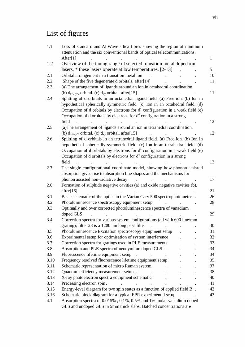
attenuation and the six conventional bands of optical telecommunications. After[1] . . . . . . . . 1
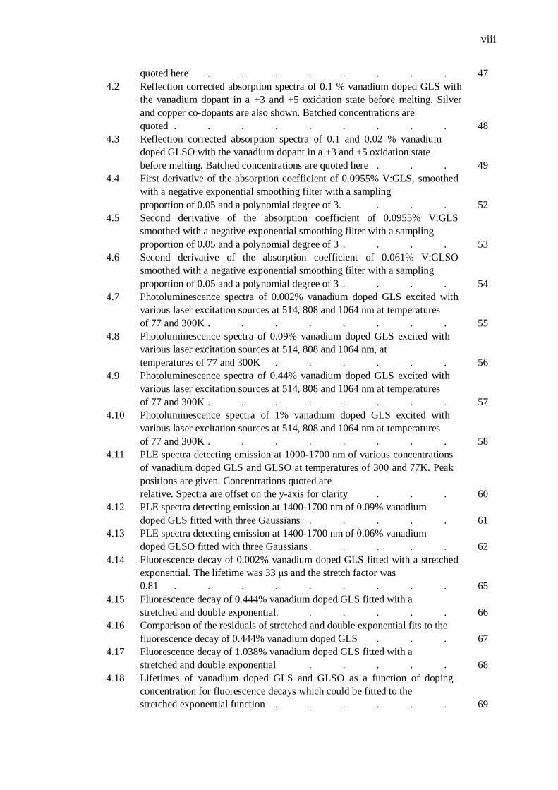
1.2 Overview of the tuning range of selected transition metal doped ion lasers, * these lasers operate at low temperatures. [2-13] . . 5
2.1 Orbital arrangement in a transition metal ion . . . . 10 2.2 Shape of the five degenerate d orbitals, after[14] . . . 11 2.3 (a) The arrangement of ligands around an ion in octahedral coordination.
(b) dx^2-y^2 orbital. (c) dxy orbital. after[15] . . . . 11 2.4 Splitting of d orbitals in an octahedral ligand field. (a) Free ion. (b) Ion in
hypothetical spherically symmetric field. (c) Ion in an octahedral field. (d) Occupation of d orbitals by electrons for d4 configuration in a weak field (e) Occupation of d orbitals by electrons for d4 configuration in a strong field . . . . . . . . . 12
2.5 (a)The arrangement of ligands around an ion in tetrahedral coordination. (b) dx^2-y^2 orbital. (c) dxy orbital. after[15] . . . . 12
2.6 Splitting of d orbitals in an tetrahedral ligand field. (a) Free ion. (b) Ion in hypothetical spherically symmetric field. (c) Ion in an tetrahedral field. (d) Occupation of d orbitals by electrons for d4 configuration in a weak field (e) Occupation of d orbitals by electrons for d4 configuration in a strong field . . . . . . . . . 13
2.7 The single configurational coordinate model, showing how phonon assisted absorption gives rise to absorption line shapes and the mechanisms for phonon assisted non-radiative decay . . . . . 17
2.8 Formation of sulphide negative cavities (a) and oxide negative cavities (b), after[16] . . . . . . . . 21
3.1 Basic schematic of the optics in the Varian Cary 500 spectrophotometer . 26 3.2 Photoluminescence spectroscopy equipment setup . . . 28 3.3 Optimally and over corrected photoluminescence spectra of vanadium
doped GLS . . . . . . . . 29 3.4 Correction spectra for various system configurations (all with 600 line/mm
grating); filter 28 is a 1200 nm long pass filter . . . . 30 3.5 Photoluminescence Excitation spectroscopy equipment setup . . 31 3.6 Experimental setup for optimisation of system interference . . 32 3.7 Correction spectra for gratings used in PLE measurements . . 33 3.8 Absorption and PLE spectra of neodymium doped GLS . . . 34 3.9 Fluorescence lifetime equipment setup . . . . . 34 3.10 Frequency resolved fluorescence lifetime equipment setup . . 35 3.11 Schematic representation of micro Raman system . . . 37 3.12 Quantum efficiency measurement setup . . . . . 38 3.13 X-ray photoelectron spectra equipment schematic . . . 40 3.14 Precessing electron spin . . . . . . . 41 3.15 Energy-level diagram for two spin states as a function of applied field B . 42 3.16 Schematic block diagram for a typical EPR experimental setup . . 43 4.1 Absorption spectra of 0.015% , 0.1%, 0.5% and 1% molar vanadium doped
GLS and undoped GLS in 5mm thick slabs. Batched concentrations are
viii
quoted here . . . . . . . . 47 4.2 Reflection corrected absorption spectra of 0.1 % vanadium doped GLS with
the vanadium dopant in a +3 and +5 oxidation state before melting. Silver and copper co-dopants are also shown. Batched concentrations are quoted . . . . . . . . . 48
4.3 Reflection corrected absorption spectra of 0.1 and 0.02 % vanadium doped GLSO with the vanadium dopant in a +3 and +5 oxidation state before melting. Batched concentrations are quoted here . . . 49
4.4 First derivative of the absorption coefficient of 0.0955% V:GLS, smoothed with a negative exponential smoothing filter with a sampling proportion of 0.05 and a polynomial degree of 3. . . . 52
4.5 Second derivative of the absorption coefficient of 0.0955% V:GLS smoothed with a negative exponential smoothing filter with a sampling proportion of 0.05 and a polynomial degree of 3 . . . . 53
4.6 Second derivative of the absorption coefficient of 0.061% V:GLSO smoothed with a negative exponential smoothing filter with a sampling proportion of 0.05 and a polynomial degree of 3 . . . . 54
4.7 Photoluminescence spectra of 0.002% vanadium doped GLS excited with various laser excitation sources at 514, 808 and 1064 nm at temperatures of 77 and 300K . . . . . . . . 55
4.8 Photoluminescence spectra of 0.09% vanadium doped GLS excited with various laser excitation sources at 514, 808 and 1064 nm, at temperatures of 77 and 300K . . . . . . 56
4.9 Photoluminescence spectra of 0.44% vanadium doped GLS excited with various laser excitation sources at 514, 808 and 1064 nm at temperatures of 77 and 300K . . . . . . . . 57
4.10 Photoluminescence spectra of 1% vanadium doped GLS excited with various laser excitation sources at 514, 808 and 1064 nm at temperatures of 77 and 300K . . . . . . . . 58
4.11 PLE spectra detecting emission at 1000-1700 nm of various concentrations of vanadium doped GLS and GLSO at temperatures of 300 and 77K. Peak positions are given. Concentrations quoted are relative. Spectra are offset on the y-axis for clarity . . . 60
4.12 PLE spectra detecting emission at 1400-1700 nm of 0.09% vanadium doped GLS fitted with three Gaussians . . . . . 61
4.13 PLE spectra detecting emission at 1400-1700 nm of 0.06% vanadium doped GLSO fitted with three Gaussians . . . . . 62
4.14 Fluorescence decay of 0.002% vanadium doped GLS fitted with a stretched exponential. The lifetime was 33 µs and the stretch factor was 0.81 . . . . . . . . . 65
4.15 Fluorescence decay of 0.444% vanadium doped GLS fitted with a stretched and double exponential. . . . . . 66
4.16 Comparison of the residuals of stretched and double exponential fits to the fluorescence decay of 0.444% vanadium doped GLS . . . 67
4.17 Fluorescence decay of 1.038% vanadium doped GLS fitted with a stretched and double exponential . . . . . 68
4.18 Lifetimes of vanadium doped GLS and GLSO as a function of doping concentration for fluorescence decays which could be fitted to the stretched exponential function . . . . . . 69

ix
4.19 R2 of stretched and constrained double exponential fits as a function of vanadium concentration . . . . . . . 70
4.20 Stretch factor as a function of vanadium doping concentration in GLS and GLSO . . . . . . . . 71
4.21 Graphical representation of I(t) and tI(t) for 0.096% vanadium doped GLS 73 4.22 Average lifetime of vanadium doped GLS as a function of doping
concentration. The lines are a guide for the eye . . . . 74 4.23 In phase FRS measurement of V:GLS at various concentrations.
Excitation was at 1064 nm unless stated otherwise . . . 76 4.24 Test of continuous lifetime analysis technique using a computer
generated continuous lifetime distribution . . . . 77 4.25 Exponential decay for the artificial lifetime distribution fitted to the
continuous lifetime distribution model . . . . . 78 4.26 Some fluorescence decays of V:GLS fitted with a continuous lifetime
distribution . . . . . . . . 79 4.27 Lifetime distribution in V:GLS at various vanadium concentrations . 80 4.28 Emission spectra of 0.0023% V:GLS at various temperatures fitted with
a 4 parameter Gaussian 83 4.29 Emission decay of 0.0023% V:GLS at 6.5 and 300 K together with
stretched exponential fits . . . . . . 85 4.30 Experimental data for the total decay rate of 0.0023% vanadium doped
GLS as a function of temperature fitted to the model of Struck and Fonger and the non-radiative decay rate as a function of temperature was calculated from the fit parameters . . . . . 86
4.31 Temperature dependence of the quantum efficiency of 0.0023% V:GLS calculated from the Struck-Fonger model . . . . 87
4.32 Emission spectrum of 0.0023% V:GLS taken with an integrating sphere and fitted to a Gaussian . . . . . . . 88
4.33 Quantum efficiency of vanadium doped GLS as a function of doping concentration measured with an integrating sphere . . . 89 4.34 X-ray photoelectron spectra of 1% vanadium doped GLS . . 91 4.35 Close up of vanadium peak for X-ray photoelectron spectra of 1% vanadium doped GLS . . . . . . . 91 4.36 X-band EPR spectra (9.5 GHz) of 1% and 0.5% vanadium doped GLS at 300K . . . . . . . . . 93 4.37 X-band EPR spectra (9.5 GHz) of 0.0023% vanadium doped GLS at 20 and 80K . . . . . . . . 94 4.38 Energy terms of a tetrahedral d2 ion plotted as a function of Dq/B . 101 4.39 Tanabe-Sugano diagram of the tetrahedral d2 configuration, the Dq/B
value calculated is shown. The spin forbidden energy levels were calculated with C/B=6.5 . . . . . . . 102
4.40 Tanabe-Sugano diagram of a octahedral d2 ion, the Dq/B value calculated from absorption spectra is shown. The spin forbidden energy levels were calculated with C/B=4.5 . . . . . . . 105
4.41 Tanabe-Sugano diagram of the tetrahedral d3 configuration. The spin forbidden energy levels were calculated with C/B=4.63 . . . 106
4.42 Tanabe-Sugano diagram of the octahedral d3 configuration. The spin forbidden energy levels were calculated with C/B=4.5 . . . 109
x
5.1 Absorption spectra of 0.1 to 1% molar titanium doped GLS and un- doped GLS in 3mm thick slabs . . . . . . 113
5.2 Absorption spectra of 0.05 to 1% molar titanium doped GLSO and un- doped GLSO in 3mm thick slabs. . . . . . 114
5.3 Second derivative of the absorption coefficient of 0.5% Ti:GLS and 0.5% Ti:GLSO . . . . . . . . 115
5.4 Photoluminescence spectra of 0.1% titanium doped GLS and GLSO excited with a 5mW 633 nm laser source . . . . 117
5.5 PLE spectra of 0.1% Ti:GLS and 0.1% Ti:GLSO. Emission was detected at 1000-1700 nm and the excitation source was dispersed with a 1200 line/mm blazed grating . . . . . . . 118
5.6 Fluorescence decay of 0.05% titanium doped GLS excited with a 10 mW 658 nm laser sourc fitted with a stretched exponential. The lifetime was 67 µs and the stretch factor was 0.5 . . . . . 119
5.7 Fluorescence decay of 1% titanium doped GLS excited with a 10 mW 658 nm laser sourc fitted with a stretched and double exponential. . 120
5.8 Fluorescence decay of 0.05% titanium doped GLSO excited with a 10 mW 658 nm laser source fitted with a stretched exponential. The lifetime was 97 µs and the stretch factor was 0.5 . . . . 120
5.9 Fluorescence decay of 1% titanium doped GLSO excited with a 10 mW 658 nm laser source fitted with a stretched exponential. The lifetime was 60 µs and the stretch factor was 0.5 . . . . . 121
5.10 Coefficient of determination of stretched exponential fit as a function of titanium concentration in GLS and GLSO . . . . 121
5.11 Lifetimes of titanium doped GLS and GLSO as a function of doping concentration. The emission decays were fitted with the stretched exponential model . . . . . . . 122
5.12 Lifetime distribution in Ti:GLS as a function of titanium concentration . 123 5.13 Lifetime distribution in Ti:GLSO as a function of titanium concentration . 124 5.14 Absorption spectra of 0.02% (molar) nickel doped GLS and un-doped
GLS in 5 mm thick slabs . . . . . . 125 5.15 Photoluminescence spectrum of 0.02% nickel doped GLS excited with a
5mW, 633 nm laser source . . . . . . 128 5.17 PLE spectra detecting emission at 1000-1700 nm of 0.02% nickel doped
GLS . . . . . . . . . 129 5.17 Fluorescence decay of 0.02% nickel doped GLS and GLSO exciting with
a 10 mW 658 nm laser source fitted with stretched exponentials . . 130 5.18 Absorption spectra of 1% (molar) bismuth doped GLS and un-doped
GLS in 5 mm thick slabs . . . . . . 131 5.19 Photoluminescence spectrum of 1% bismuth doped GLS excited with a
5mW 633 nm laser source . . . . . . 133 5.20 PLE spectra detecting emission at 1000-1700 nm of 1% bismuth doped
GLS . . . . . . . . . 135 5.21 Fluorescence decay of 1% bismuth doped GLS exciting with a CW 10 mW,
658 nm laser source and fitted with a double exponential and the continuous lifetime distribution model . . . . . 136
5.22 Lifetime distribution in the emission decay of 1% bismuth doped GLS . 137 6.1 Schematic of waveguide writing process . . . . . 143 6.2 Guided mode profile setup . . . . . . 144
xi
6.3 Transmission optical micrographs (a) and near-field guided mode at 633 nm (b) of waveguides written at a focus depth of ~400 µm into the GLS sample at various pulse energies and a translation speed of 200 µm/s. The arrow shows the propagation direction of the laser used to write the waveguides . . . . . . . . 145
6.4 Height, width and aspect ratio of waveguides as a function of writing pulse energy for waveguides written at a depth of 400 µm in GLS. The lines are a guide for the eye . . . . . . . 146
6.5 Transmission optical micrographs (a), guided mode at 633 nm (b) and reflection optical micrographs (c) of waveguides written at a focal depth of ~100 µm into GLS at various pulse energies and translation speeds . 148
6.6 Height, width and aspect ratio of waveguides as a function of writing pulse energy for waveguides written at a depth of ~100 µm in GLS at various translation speeds . . . . . . . 149
6.7 Transmission optical micrographs (a), guided mode at 633 nm (b) and reflection optical micrographs (c) of waveguides written at a focal depth of ~300 µm into GLSO at various pulse energies and translation speeds . 150
6.8 Height, width and aspect ratio of waveguides as a function of writing pulse energy for waveguides written at a depth of ~300 µm in GLSO at various translation speeds . . . . . . . 151
6.9 Quantitative phase microscopy setup . . . . . 153 6.10 Optical micrograph (I) and quantitative phase image (II) of waveguides
written at a translation speed of 200 µm/s and pulse energies of 1.74 µJ (a and b), 1.26 µJ (c and d), 0.84 µJ (e and f), 0.42 µJ (g and h), 0.21 µJ (i and j). The images were taken in the axis the waveguides were written. . 154
6.11 Optical micrograph (I) and quantitative phase image (II) of waveguides written at a depth of 100 µm with pulse energies and speeds of 0.28 µJ and 50 µm/s (a), 0.28 µJ and 100 µm/s (b), 0.28 µJ and 200 µm/s (c), 0.32 µJ and 50 µm/s (d), 0.32 µJ and 100 µm/s (e), 0.32 µJ and 200 µm/s (f), 0.36 µJ and 50 µm/s (g), 0.36 µJ and 100 µm/s (h), 0.36 µJ and 200 µm/s (i), 0.4 µJ/ and 50 µm/s (j), 0.4 µJ and 100 µm/s (k) respectively . 154
6.12 Emulated differential interference contrast image from quantitative phase image in figure 6.12 II . . . . . . . 155
6.13 Phase change profile of a waveguide written with 0.84 µJ/pulse, 200 µm/s translation speed and a depth of 400 µm together with the (assumed to be linear) background phase change that was subtracted from the phase change data . . . . . . 156
6.14 Refractive index change profile as a function of writing pulse energy for waveguides written into the GLS sample at a depth of ~100 µm at translation speeds of 50, 100 and 200 µm/s . . . . 156
6.15 Index change profile of a waveguide written with a pulse energy of 0.4 µJ and a translation speed of 50 µm/s scaled and superimposed on to its transmission optical micrograph . . . . . . 158
6.16 Refractive index change profile as a function of writing pulse energy for waveguides written into the GLS sample at a depth of ~400 µm . . 159
6.17 Peak index change as a function of writing pulse energy for waveguides written at a depth of 100 µm (a) and 400 µm (b) . . . . 160
6.18 Micro-Raman spectra of waveguides written at pulse energies of 1.75 µJ and 1.26 µJ and two regions of unexposed glass. The top image shows

xii
the position at which each Raman spectrum was taken . . . 161 6.19 Waveguide transmittance measurement setup . . . . 162 6.20 Transmission spectra of waveguides written in GLS at a depth of 400 µm
and a translation speed of 200 µm/s . . . . . 163 6.21 Waveguide loss measurements using the Fabry-Perot resonance method . 164 6.22 Fabry-Perot scan of a waveguide written with at 0.36 µJ/pulse and 50
µm/s translation speed . . . . . . . 165 6.23 Waveguide losses in the GLS sample as a function of writing pulse energy
at various translation speeds. Lines are a guide for the eye . . 167 6.24 Waveguide losses in GLSO sample as a function of writing pulse energy
at various translation speeds. Lines are a guide for the eye . . 168 6.25 Illustration of self-focusing (a), plasma defocusing (b) and a numerical
simulation of filamentation (c).[17] . . . . . 170 6.26 Waveguide formation mechanism in GLS at pulse energies > ~0.2
µJ/pulse (A-type) and GLS at pulse energies < ~0.2 µJ/pulse (B-type) . 173 6.27 Schematic diagram of the photoionisation of an electron in a Coulomb well
for different values of the Keldysh parameter leading to tunnelling (a), an intermediate scheme (b) and multi-photon ionisation (c); after
[18] . . . . . . . . . 174 6.28 Schematic diagram of avalanche ionisation, after[18] . . . 175 6.29 Schematic of the experimental setup used to measure ultra short pulse
broadening in GLS waveguides . . . . . . 177 6.30 Output energy as a function of input energy for a waveguide written with a
pulse energy of 1.26 µJ. The high linearity indicates negligible two photon absorption . . . . . . . 179
6.31 Spectra of 1540 nm 200 fs laser beam coupled into an 12 mm GLS waveguide, that was written with a pulse energy of 1.75 µJ, as a function of input beam pulse energy . . . . . . 180
6.32 FWHM and peak position of spectra given in figure 6.31. The FWHM is attributed to the left vertical axis and the peak positions are attributed to the right vertical axis . . . . . . . 181
6.33 Spectra of 1540 nm 200 fs laser beam coupled into an 12 mm GLS waveguide written with a pulse energy of 1.26 µJ as a function of input beam pulse energy . . . . . . . 182
6.34 FWHM and peak position of spectra given in figure 6.33 The FWHM is attributed to the left vertical axis and the peak positions are attributed to the right vertical axis . . . . . . . 183
6.35 Spectra of 1600 nm, 300 fs laser beam coupled into an 11 mm GLS waveguide, that was written with a pulse energy of 1.26 µJ, as a function of input beam pulse energy . . . . . . 184
6.36 FWHM and peak position of spectra given in figure 6.35 . . 185

xiii
List of tables 1.1 Optical properties of silica, ZBLAN, As2S3 and GLS glass . . .3 2.1 A character table of the Oh group, after[19] . . . . 15 3.1. Melting point and density of various melt components[20] . . 23 3.2. Transition metals dopants and their compounds . . . . 24 3.3 Molar percentages of melt components for initial vanadium doped GLS melts 24 3.4. Molar percentages of melt components for “dopant glasses” . . 25 3.5. Molar percentages of melt components for vanadium doped GLS glass
doped with “dopant glasses” and co-doped with copper and silver . 25 3.6 Molar percentages of melt components for vanadium doped GLSO glass
doped with “dopant glasses” . . . . . . 25 3.7. Summary of spectroscopic techniques used in this work . . . 44 4.1 Relative V2+ ion concentration for vanadium doped GLS samples . . 49 4.2 Peak amplitude and relative signal-to-noise ratio for Gaussian peaks and
some derivatives . . . . . . . 51 4.3 Photoluminescence peak positions (nm) for varying concentration,
excitation wavelength and temperature . . . . . 56 4.4 Summary of photoluminescence from vanadium in +1,2+ and 3+
oxidation states in various hosts . . . . . 59 4.5 Lifetimes of various concentrations of V:GLS, calculated by FRS and TRS.
† TRS lifetime calculated from stretched exponential fit (excited at 1064 nm), ‡ TRS lifetime calculated from average lifetime (excited at 1064 nm). †† 633 nm excitation . . . . . . 75
4.6 Lifetimes identified by continuous lifetime distribution, double exponential and stretched exponential fits to the fluorescence decay of V:GLS at various vanadium concentrations . . . . 80
4.7 Initial estimate and fit parameters for Struck-Fonger fit . . . 86 4.9 Details of vanadium samples with their respective quantum efficiency, peak
emission wavelength (λmax), emission bandwidths (∆λ), emission lifetimes (τ), emission cross sections (σem) and σemτ products at room
temperature . . . . . . . . 89 4.10 Overview of the spectroscopic parameters for various laser materials
compared to V:GLS. * These lasers only operate at low temperatures . 90 4.11 Summary of charge transfer transitions in Cr6+ and V5+ . . . 96 4.12 Summary of absorption transitions of V4+ . . . . 96 4.13 Summary of absorption transitions of V3+ . . . . 97 4.14 Summary of absorption transitions of V2+ . . . . 98 4.15 Summary of absorption transitions of V+ . . . . . 99 4.16 Energy matrix for the 3T1(
3F,3P) state . . . . . 100 4.17 Energy matrix for the 1E(1D,1G) state . . . . . 101 4.18 Crystal field parameters calculated for a d2 ion in tetrahedral coordination 103 4.19 Energy matrix for the 3T1(
3F,3P) state . . . . . 103 4.20 Energy matrix for the 1E(1D,1G) state . . . . . 104 4.21 Crystal field parameters calculated for a d2 ion in tetrahedral coordination 106 4.22 Dq and B crystal field parameters calculated for the octahedral d3
configuration. The energy of the 4T1(4P) level was calculated from the
Tanabe-Sugano model . . . . . . . 108

xiv
4.23 B and C/B crystal field parameters calculated for the octahedral d3 configuration 110 5.1 Absorption details for titanium in a variety of glasses and in sapphire . 116 5.2 Absorption details for nickel in a variety of glass and crystal hosts . 127 5.3 Absorption details for bismuth in a variety of glass and crystal hosts
†Tentative assignment . . . . . . . 132 5.4 Emission details for bismuth in a variety of glass and crystal hosts
†Tentative assignment . . . . . . . 134 5.5 Emission lifetime details for bismuth in a variety of glass and crystal hosts
†Tentative assignment ‡Lasing demonstrated . . .
xv
Acknowledgements I would like to thank everyone who helped me with this project, especially after the Mountbatten fire, their name are too numerous to mention here. In particular I would like to thank my supervisor Prof. Dan Hewak for his technical support and guidance and my co-supervisor Dr. Richard Curry for his continued support after moving to another institution one year into my PhD. I would also like to thank Prof. Harvey Rutt for assisting my work his seemingly bottomless knowledge of spectroscopy, Weijia Yang for his assistance with the waveguide fabrication and characterisation. Sincere thanks to Dr. Eleanor Tarbox for going through my thesis with a fine tooth comb. Thanks to Kenton Knight for helping me to melt glass, Dr. N. Blanchard for his assistance with the XPS measurements and Dr. Giampaolo D'Alessandro for his assistance with the continuous lifetime distribution model.
Chapter 1 Introduction 1
Chapter 1
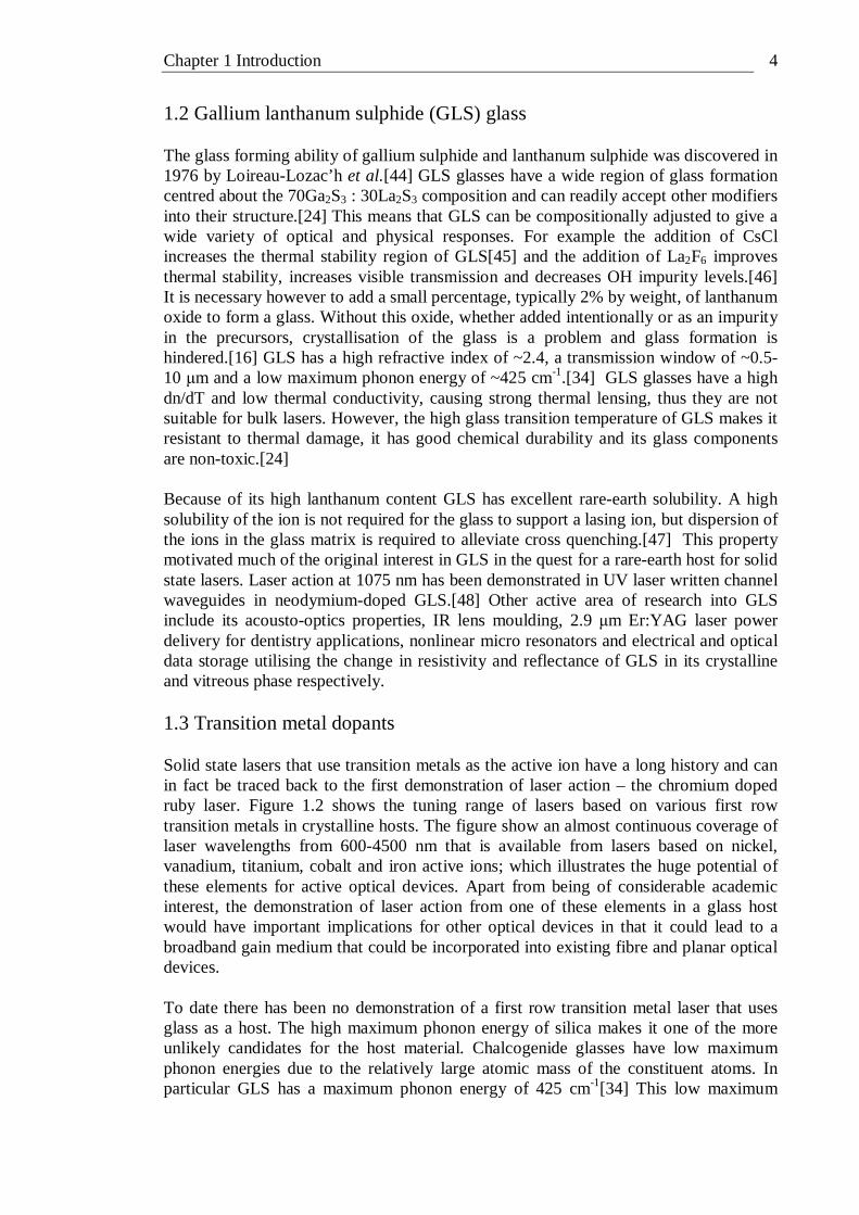
Introduction 1.1 Motivation Over the past few decades silica fibre has revolutionised the way in which we communicate by allowing low cost, high bandwidth transmission of data over long distances. This has enabled millions of people around the world access to data resources like the World Wide Web as well as voice and video phone. Further improvements to the data bandwidth available to home users could revolutionise the way media such as news, films and music are accessed. An example of this is the growing implementation of media-on-demand.[21] The invention of the erbium doped fibre amplifier (EDFA) in 1985[22] was instrumental in allowing long distance data transmission through silica fibre and was a significant improvement on electronic repeaters which required the conversion between optical and electronic signals. By a quirk of nature an emission band of erbium, which dictates the gain bandwidth of the EDFA, sits neatly in the low loss window of silica. The technology behind silica fibre is now mature; its structure and properties are well understood and the loss achievable in silica fibre comes close to its theoretical minimum.
Wavelength (µm)
1.30 1.35 1.40 1.45 1.50 1.55 1.60 1.65
Loss
(dB
km-1
)
0.15
0.20
0.25
0.30
0.35
Standard fibreAllWave fibre
U-b
and
L-b
and
C-b
and
S-b
and
E-b
and
O-b
and
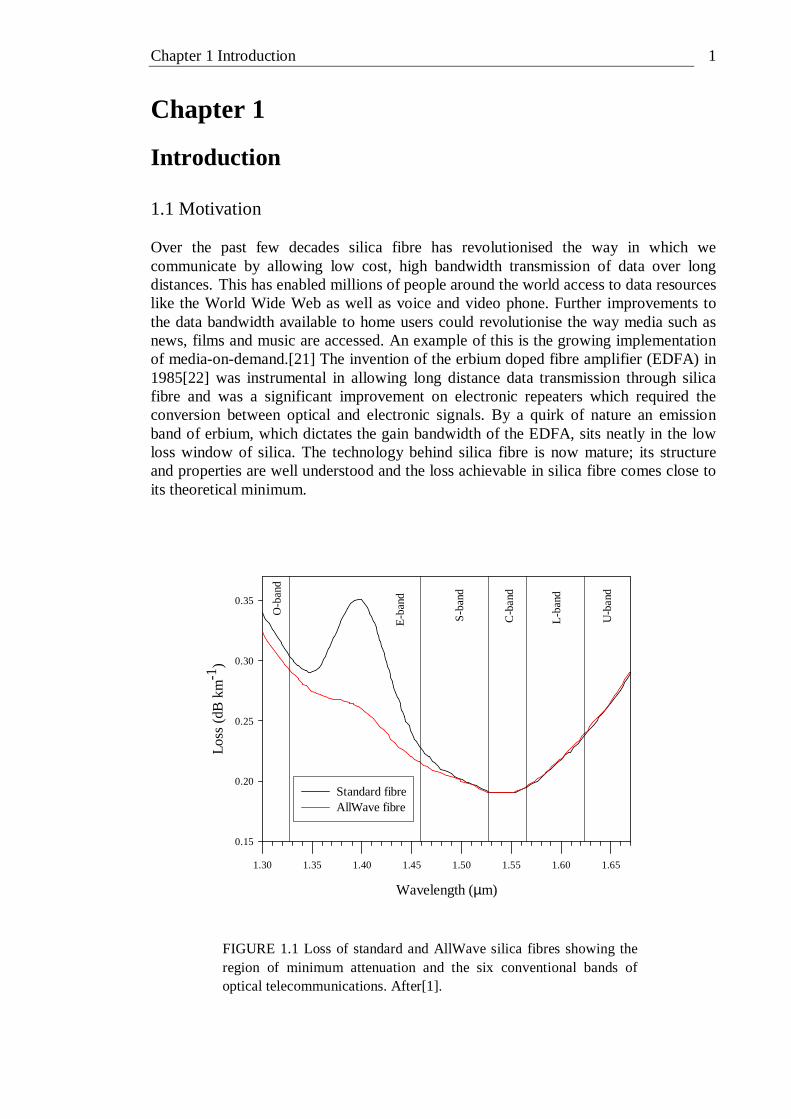
FIGURE 1.1 Loss of standard and AllWave silica fibres showing the region of minimum attenuation and the six conventional bands of optical telecommunications. After[1].
Chapter 1 Introduction 2
Until recently the presence of the hydroxyl impurity in silica introduced an overtone absorption around 1400 nm which effectively divided the region of lowest attenuation into two separate windows. In 1998, Lucent technologies introduced the AllWave fibre which contains less than one part per billion hydroxyl ions.[23] This ultra dry fibre effectively gives one continuous low loss window spanning ~1260 to 1670 nm, as shown in figure 1.1. The gain bandwidth of the EDFA spans only a small fraction of this continuous low loss window. Doping with other rare earths could allow wavelengths not covered by the EDFA to be used, but problems associated with the vibrational structure of silica prevent its use as an amplifier medium when doped with ions such as praseodymium, thulium and dysprosium.[24] Silica glass is by a long way the most favourable material to use for long distance optical fibre telecommunications. However, there are aspects of the properties of silica which make it unsuitable for certain applications. For instance the low rare earth solubility of silica means that the interaction length of active devices based on rare-earth doped silica is relatively long. The high phonon energy of silica means that transitions of many rare earth dopants decay non-radiatively. The relatively low non-linear refractive index of silica means that non-linear devices based on silica require relatively high intensities in order to function. The transmission wavelength of silica is also limited to 2 µm. These shortcomings of silica have merited the investigation of a variety of novel glasses for optical device applications. These include phosphate, heavy metal oxide (HMO), fluoride and chalcogenide glasses. The high energy storage and extraction characteristics of phosphate glasses make them suitable for high power laser applications such as fusion research.[25] The national ignition facility (NIF) at the Lawrence Livermore National Laboratory, (California, USA) uses Nd doped phosphate glass as a gain medium. When completed the NIF is expected to produce ~ns pulses with energies of ~2 MJ and peak powers of ~500 TW.[26] HMO glasses are arbitrarily defined as those glasses containing over 50 cation % of bismuth and/or lead. They are believed to have the highest refractive indexes of any oxide glass and are also characterised by high density, high thermal expansion, low transformation temperature and excellent infrared transmission up to ~6 µm.[27] A 2R regenerator (see section 6.1.3.3 for a description) that exploits the nonlinearity of bismuth oxide fibre has been demonstrated.[28] The fluoride glass ZBLAN is based on the fluorides of Zr, Ba, La, Al and Na. A loss of 0.45 dB km-1 at 2.35 µm has been achieved for ZBLAN fibre.[29] Such fibres area now used for various passive applications requiring the handling of IR signal. In this respect, fluoride fibres are complementary to silica fibres when the wavelength exceeds 2 µm. Laser power delivery is another field of application for these fibres, for example Er:YAG laser at 2.9 µm attracts a growing interest for dental applications.[30] Chalcogenide glasses contain a chalcogen element (sulphur, selenium or tellurium) as a substantial constituent. Oxygen is also a chalcogen but it is not usually included in the definition of chalcogenide glasses because oxide glasses form a large group with distinctly different properties to glasses formed from the other chalcogen elements. One of the principle differences between oxide and chalcogenide glasses is their bandgap
Chapter 1 Introduction 3
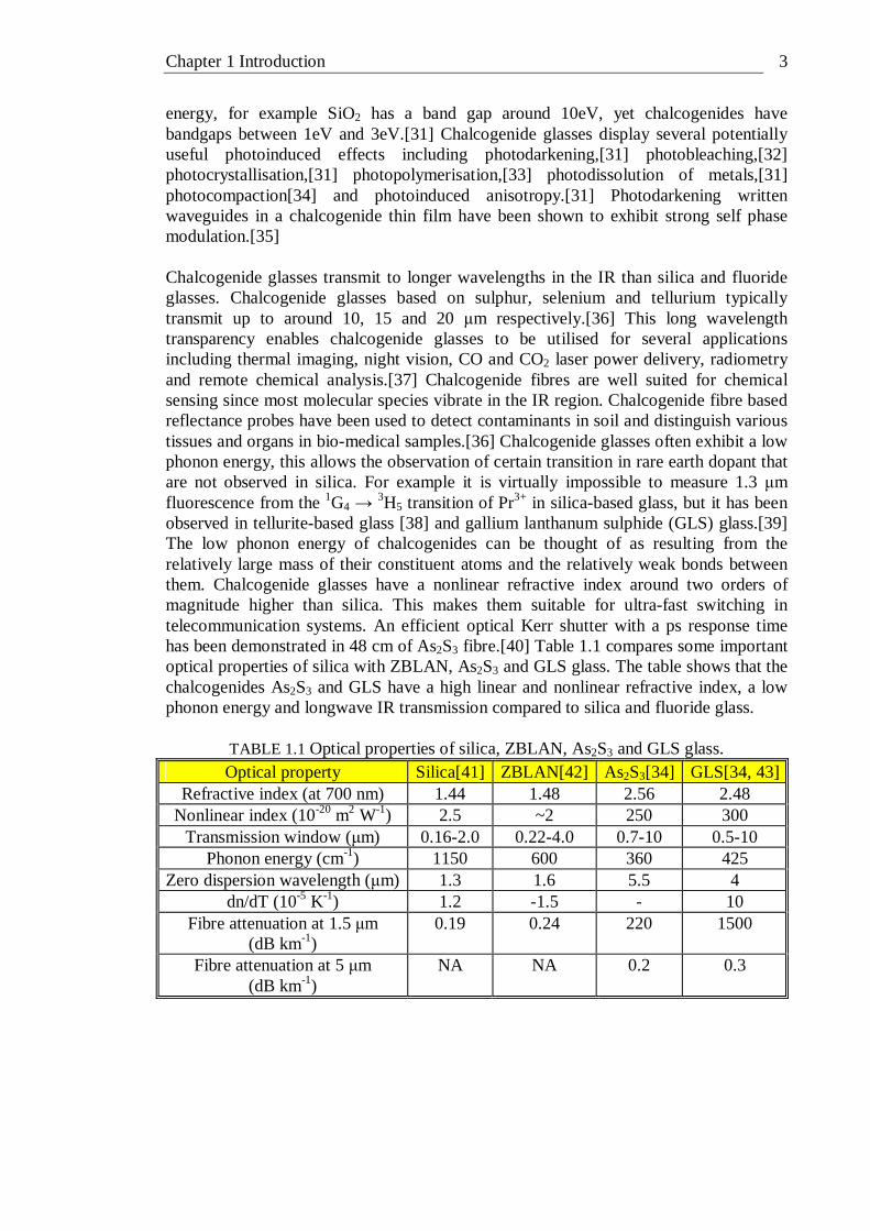
energy, for example SiO2 has a band gap around 10eV, yet chalcogenides have bandgaps between 1eV and 3eV.[31] Chalcogenide glasses display several potentially useful photoinduced effects including photodarkening,[31] photobleaching,[32] photocrystallisation,[31] photopolymerisation,[33] photodissolution of metals,[31] photocompaction[34] and photoinduced anisotropy.[31] Photodarkening written waveguides in a chalcogenide thin film have been shown to exhibit strong self phase modulation.[35] Chalcogenide glasses transmit to longer wavelengths in the IR than silica and fluoride glasses. Chalcogenide glasses based on sulphur, selenium and tellurium typically transmit up to around 10, 15 and 20 µm respectively.[36] This long wavelength transparency enables chalcogenide glasses to be utilised for several applications including thermal imaging, night vision, CO and CO2 laser power delivery, radiometry and remote chemical analysis.[37] Chalcogenide fibres are well suited for chemical sensing since most molecular species vibrate in the IR region. Chalcogenide fibre based reflectance probes have been used to detect contaminants in soil and distinguish various tissues and organs in bio-medical samples.[36] Chalcogenide glasses often exhibit a low phonon energy, this allows the observation of certain transition in rare earth dopant that are not observed in silica. For example it is virtually impossible to measure 1.3 µm fluorescence from the 1G4 → 3H5 transition of Pr3+ in silica-based glass, but it has been observed in tellurite-based glass [38] and gallium lanthanum sulphide (GLS) glass.[39] The low phonon energy of chalcogenides can be thought of as resulting from the relatively large mass of their constituent atoms and the relatively weak bonds between them. Chalcogenide glasses have a nonlinear refractive index around two orders of magnitude higher than silica. This makes them suitable for ultra-fast switching in telecommunication systems. An efficient optical Kerr shutter with a ps response time has been demonstrated in 48 cm of As2S3 fibre.[40] Table 1.1 compares some important optical properties of silica with ZBLAN, As2S3 and GLS glass. The table shows that the chalcogenides As2S3 and GLS have a high linear and nonlinear refractive index, a low phonon energy and longwave IR transmission compared to silica and fluoride glass.
TABLE 1.1 Optical properties of silica, ZBLAN, As2S3 and GLS glass. Optical property Silica[41] ZBLAN[42] As2S3[34] GLS[34, 43]
Refractive index (at 700 nm) 1.44 1.48 2.56 2.48 Nonlinear index (10-20 m2 W-1) 2.5 ~2 250 300
Transmission window (µm) 0.16-2.0 0.22-4.0 0.7-10 0.5-10 Phonon energy (cm-1) 1150 600 360 425
Zero dispersion wavelength (µm) 1.3 1.6 5.5 4 dn/dT (10-5 K-1) 1.2 -1.5 - 10
Fibre attenuation at 1.5 µm (dB km-1)
0.19 0.24 220 1500
Fibre attenuation at 5 µm (dB km-1)
NA NA 0.2 0.3
Chapter 1 Introduction 4
1.2 Gallium lanthanum sulphide (GLS) glass The glass forming ability of gallium sulphide and lanthanum sulphide was discovered in 1976 by Loireau-Lozac’h et al.[44] GLS glasses have a wide region of glass formation centred about the 70Ga2S3 : 30La2S3 composition and can readily accept other modifiers into their structure.[24] This means that GLS can be compositionally adjusted to give a wide variety of optical and physical responses. For example the addition of CsCl increases the thermal stability region of GLS[45] and the addition of La2F6 improves thermal stability, increases visible transmission and decreases OH impurity levels.[46] It is necessary however to add a small percentage, typically 2% by weight, of lanthanum oxide to form a glass. Without this oxide, whether added intentionally or as an impurity in the precursors, crystallisation of the glass is a problem and glass formation is hindered.[16] GLS has a high refractive index of ~2.4, a transmission window of ~0.5-10 µm and a low maximum phonon energy of ~425 cm-1.[34] GLS glasses have a high dn/dT and low thermal conductivity, causing strong thermal lensing, thus they are not suitable for bulk lasers. However, the high glass transition temperature of GLS makes it resistant to thermal damage, it has good chemical durability and its glass components are non-toxic.[24] Because of its high lanthanum content GLS has excellent rare-earth solubility. A high solubility of the ion is not required for the glass to support a lasing ion, but dispersion of the ions in the glass matrix is required to alleviate cross quenching.[47] This property motivated much of the original interest in GLS in the quest for a rare-earth host for solid state lasers. Laser action at 1075 nm has been demonstrated in UV laser written channel waveguides in neodymium-doped GLS.[48] Other active area of research into GLS include its acousto-optics properties, IR lens moulding, 2.9 µm Er:YAG laser power delivery for dentistry applications, nonlinear micro resonators and electrical and optical data storage utilising the change in resistivity and reflectance of GLS in its crystalline and vitreous phase respectively. 1.3 Transition metal dopants Solid state lasers that use transition metals as the active ion have a long history and can in fact be traced back to the first demonstration of laser action – the chromium doped ruby laser. Figure 1.2 shows the tuning range of lasers based on various first row transition metals in crystalline hosts. The figure show an almost continuous coverage of laser wavelengths from 600-4500 nm that is available from lasers based on nickel, vanadium, titanium, cobalt and iron active ions; which illustrates the huge potential of these elements for active optical devices. Apart from being of considerable academic interest, the demonstration of laser action from one of these elements in a glass host would have important implications for other optical devices in that it could lead to a broadband gain medium that could be incorporated into existing fibre and planar optical devices. To date there has been no demonstration of a first row transition metal laser that uses glass as a host. The high maximum phonon energy of silica makes it one of the more unlikely candidates for the host material. Chalcogenide glasses have low maximum phonon energies due to the relatively large atomic mass of the constituent atoms. In particular GLS has a maximum phonon energy of 425 cm-1[34] This low maximum
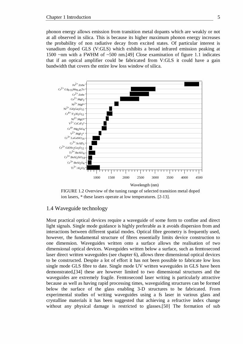
Chapter 1 Introduction 5
phonon energy allows emission from transition metal dopants which are weakly or not at all observed in silica. This is because its higher maximum phonon energy increases the probability of non radiative decay from excited states. Of particular interest is vanadium doped GLS (V:GLS) which exhibits a broad infrared emission peaking at 1500 ~nm with a FWHM of ~500 nm.[49] Close examination of figure 1.1 indicates that if an optical amplifier could be fabricated from V:GLS it could have a gain bandwidth that covers the entire low loss window of silica.
Wavelength (nm)
1000 1500 2000 2500 3000 3500 4000 4500
Ti3+:Al2O3
Cr3+:BeAl2O4
Cr3+:BeAl2SiO18
Ti3+:BeAlO4
Cr3+:Gd3Sc2Ga3O12
Cr3+:SrAlF5
Cr3+:LaGaSiO14
V2+:MgF2*
Cr4+:Mg2SiO4
V2+:CsCaF3*
Ni2+:MgO*
Cr4+:Y3Al5O12
Ni2+:Gd3Ga5O12
Ni2+:MgF*
Co2+:MgF2
Cr2+:ZnSe
Cr2+:Cd0.55Mn0.45Te
Fe2+:ZnSe
FIGURE 1.2 Overview of the tuning range of selected transition metal doped ion lasers, * these lasers operate at low temperatures. [2-13].
1.4 Waveguide technology Most practical optical devices require a waveguide of some form to confine and direct light signals. Single mode guidance is highly preferable as it avoids dispersion from and interactions between different spatial modes. Optical fibre geometry is frequently used, however, the fundamental structure of fibres essentially limits device construction to one dimension. Waveguides written onto a surface allows the realisation of two dimensional optical devices. Waveguides written below a surface, such as femtosecond laser direct written waveguides (see chapter 6), allows three dimensional optical devices to be constructed. Despite a lot of effort it has not been possible to fabricate low loss single mode GLS fibre to date. Single mode UV written waveguides in GLS have been demonstrated,[34] these are however limited to two dimensional structures and the waveguides are extremely fragile. Femtosecond laser writing is particularly attractive because as well as having rapid processing times, waveguiding structures can be formed below the surface of the glass enabling 3-D structures to be fabricated. From experimental studies of writing waveguides using a fs laser in various glass and crystalline materials it has been suggested that achieving a refractive index change without any physical damage is restricted to glasses.[50] The formation of sub
Chapter 1 Introduction 6
diffraction limited structures is feasible using a focused fs laser beam because of the nonlinear process involved in material modification. The fabrication of buried fs laser written waveguides in GLS has been demonstrated[51] and they show promise for the development of optical devices based on high quality waveguide structures in GLS. 1.5 Scope of the thesis This thesis focuses on two different, but complementary, aspects of the modification of GLS. Firstly the addition of transition metal ions as dopants is examined and their potential for use as active optical materials is explored. It is also argued that the spectroscopic analysis of transition metal ions is a useful tool for evaluating the local environment of their host. Secondly fs laser modification of GLS is investigated as a method for waveguide formation. The observation of spectral broadening indicates that these waveguides may have applications for nonlinear optical devices. The change in direction of this thesis, from investigating transition metal dopants to fs laser written waveguides, was compelled by the loss of ORC glass fabrication and characterisation facilities in a fire. Because of this certain glass samples could not be fabricated, notably vanadium doped GLSO and bismuth doped GLS, and certain characterisations, notably quantum efficiency, could not be completed on all samples. In this thesis the following are presented for the first time:
• Calculation of the crystal field parameters for a transition metal ion in GLS using the Tanabe-Sugano model
• Calculation of the lifetime distribution in a transition metal doped chalcogenide glass using the continuous lifetime distribution model.
• Quantum efficiency measurement of a transition metal ion in GLS • X-ray photoelectron spectroscopy measurement of a dopant ion in GLS • Electron paramagnetic resonance measurement of a dopant ion in GLS • The emission and emission lifetime of titanium doped GLS. • Optical characterisation of bismuth doped GLS. • Characterisation of fs laser written waveguides in GLS • Broadening of an ultra-short pulse in a GLS waveguide. • Loss measurement of a GLS waveguide using the Fabry-Perot technique. • Index change profile measurement using quantitative phase microscopy in a
GLS waveguide. The thesis is structured into seven chapters, including this introduction, chapter 1.
• Chapter 2 provides sufficient background related to the spectroscopy of transition metal ions for the understanding of chapters 3, 4 and 5.
• Chapter 3 details the melting procedures for the fabrication of transition metal doped GLS and all of the spectroscopic techniques used in the analysis of transition metal doped GLS
• Chapter 4 presents a rigorous optical characterisation of vanadium doped GLS glass. The emission lifetime and its non-exponential decay characteristics are investigated in detail. Absorptions from three spin-allowed transition and one
Chapter 1 Introduction 7
spin-forbidden transition were identified. The energy of these transitions was used to identify the oxidation state and coordination number of the vanadium ion. X-ray photoelectron spectroscopy was used to identify that vanadium exists in a broad range of oxidation states in GLS.
• Chapter 5 details the spectroscopic properties of titanium, nickel and bismuth doped GLS. Arguments based on the number of observed absorption peaks and comparisons with dopants in other hosts were used to identify the oxidation state of these dopants.
• Chapter 6 is somewhat self-contained and describes the fabrication and characterisation of buried waveguides written into GLS glass using 800 nm focused fs laser pulses. The spectral broadening of 1550 nm fs laser pulse coupled into these waveguides is also reported.
• Chapter 7 draws conclusions and identifies topics that might provide the basis for further studies.
Chapter 2 Background 8
Chapter 2
Background 2.1 Introduction The scope of this chapter is to provide sufficient background for the understanding of subsequent chapters. It begins with an introduction to absorption and lifetime measurements, then an overview of crystal field theory which describes how the energy levels of the d orbital split in the presence of a ligand or crystal field is given. Group theory is then introduced to describe how the labelling of the energy levels of a transition metal ion is arrived at. Next the single configurational coordinate model is introduced this is followed by spectral broadening mechanisms and finally some important structural properties of GLS are described. 2.2 Spectroscopy basics 2.2.1 Absorption measurements In absorption spectroscopy the experimenter observes what frequencies of radiation are absorbed from incident radiation as it passes through a sample. If light of frequency ν is absorbed, it signifies that an absorbing species of the sample has undergone a transition from a state of energy E1 to a state of energy E2 and that equation 2.1 is satisfied.[52]
12 EEh −=υ (2.1) Consider the reduction of intensity that occurs when light of intensity I passes through a slab, with infinitesimal thickness dz, of the sample. The loss of intensity dI is proportional to the thickness dz and the intensity of the incident light I and is given by:
IdzdI α−= (2.2) Where α is the absorption coefficient, which depends both on the absorbing species and the frequency of the incident light, and commonly has units of cm-1. Integrating both sides of equation 2.2 gives I as a function of z: ln(I) = -αz + C. For a sample of thickness l the difference between the incident intensity I0 at z = 0 and the intensity IT that emerges from the sample at z = l is given by ln(I0) - ln(IT) = (-α0 + C) - (-αl + C) = αl, this can be expressed as equation 2.3 which is otherwise known as the Beer-Lambert law.[19, 52]
)exp(0 lII T α−= (2.3)
If the concentration of absorbing species c is taken into account then equation 2.2 becomes:
IcdzdI σ−= (2.4)
Chapter 2 Background 9
If c is expressed as a number per unit volume then σ is the absorption cross section and has units of area. Data obtained from the spectrophotometers used in this study is in units of absorbance A:
TI
IA 0
10log= (2.5)
The absorption coefficient a was then calculated from a = A/l. Note the decadic form a of absorption coefficient is used where a = α/ ln10 = α/2.303. 2.2.2 Excited state absorption Excited state absorption (ESA) occurs when the energy sate E1, described in section 2.2.1, is not the lowest energy level of the absorbing species. In this case absorption occurs with the promotion of an electron in an excited state higher than the initial excited state. ESA needs to be addressed when considering a material as a gain medium for a laser or optical amplifier because ESA can induce parasitic loss of pump or laser radiation which increases the pump power threshold. ESA is a problem for broadband gain media in particular but it is also likely to be relevant for laser ions with multiple electronic levels, such as erbium or thulium. ESA is usually measured using the pump-probe technique[53-55] in which the transmission of a weak probe beam is measured with and without the presence of a strong pump beam. 2.2.3 Lifetime measurements In lifetime measurements the experimenter observes the emission intensity from a sample as a function of time after an initial excitation pulse, which ends at t = 0. Consider the ground state (level 1) and excited state (level 2) of an absorbing species. After an initial excitation pulse the population density in level 2 is expressed as N2 (number per unit volume). Assuming that no quenching or interaction between excited species occurs then N2, as a function of time, will decay with an exponential decay rate. The change in population density N2, as the population is transferred to level 1, can be expressed as:[56]
2212 NA
dt
dN−= (2.6)
Where A21 is the rate at which the population is transferred from level 2 to level 1. A21 has units of 1/time, and is referred to as the radiative transition rate. The solution to equation 2.6 is:
)exp( 21022 tANN −= (2.7)
Where N2
0 is the initial population density in level 2 at t = 0. Defining a time τ2 as the time taken for the population N2 to decay to 1/e of its original value and considering that the observed emission intensity I(t) is proportional to the population N2, equation 2.7 can be expressed as:
)/exp()( 20 τtItI −= (2.8)
Chapter 2 Background 10
Where I0 is the emission intensity at t = 0. The time τ2 is referred to as the lifetime of level 2. 2.3 Crystal field theory This relatively simple theory was first proposed by Bethe[57] and Van Vleck[58] but is still useful for visualising the electrostatic interaction between the orbitals of a central metal ion and the surrounding ligand field. In crystal field theory the positive ions are regarded as point charges and neutral molecules as dipoles with their negative ends directed towards the metal. Covalent bonding is completely neglected.[15] The arrangement of the orbitals in a transition metal (TM) is illustrated in figure 2.1, adapted from.[2]
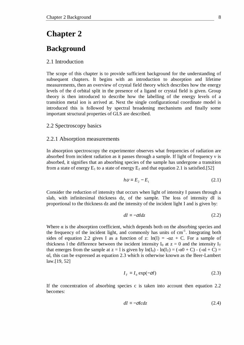
FIGURE 2.1 Orbital arrangement in a transition metal ion.
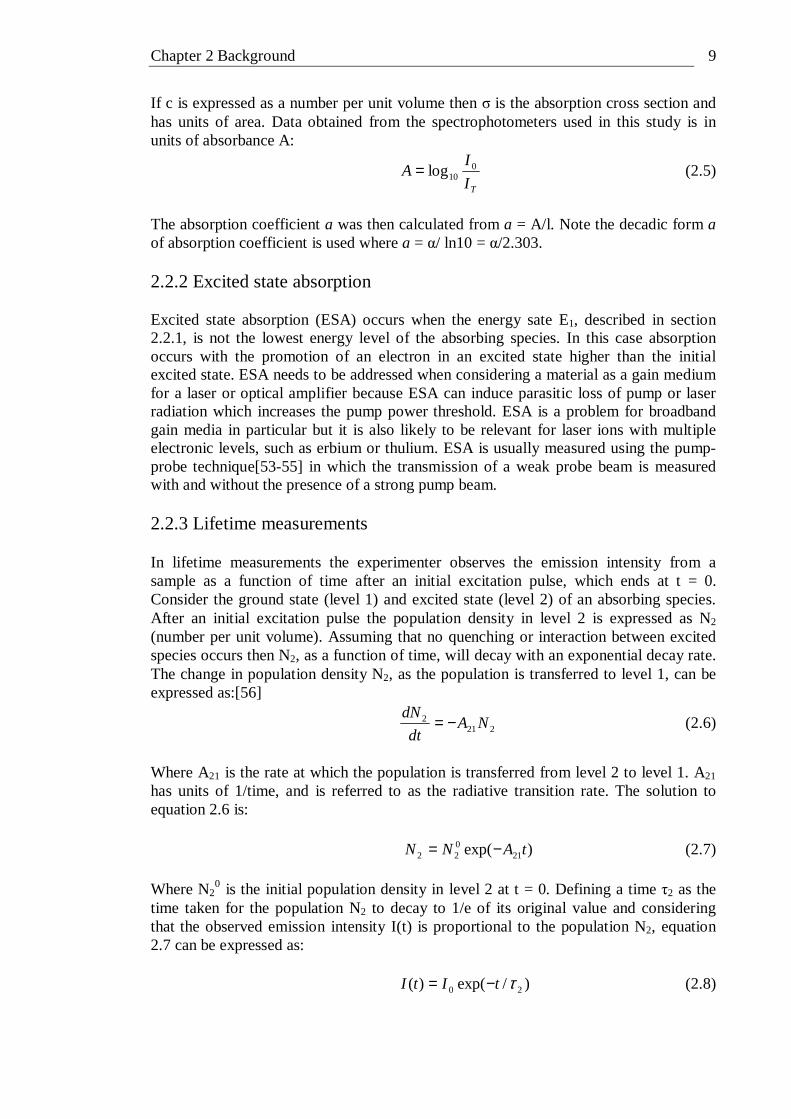
The 4s electrons are used to form chemical bonds leaving 3d electrons exposed to the electric field of neighbouring atoms, this field is also called the crystal or ligand field. Therefore the 3d electrons are strongly affected by both the strength of the neighbouring atoms electric field and their arrangement around the transition metal ion (coordination). The angular dependence of the d orbital wave function consists of five orthogonal sets of independent orbitals as illustrated in figure 2.2. The five orbitals are degenerate, in other words they have the same energy in the absence of an external electrostatic field.
Chapter 2 Background 11
x^2-y^2z^2
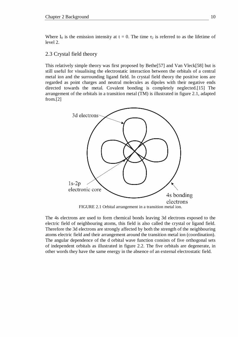
FIGURE 2.2 Shape of the five degenerate d orbitals, after[14]. When the central metal ion is surrounded by six ligands, with an axis of symmetry, the ion is said to be in octahedral coordination, this case is illustrated in figure 2.3
FIGURE 2.3 (a) The arrangement of ligands around an ion in octahedral coordination. (b) dx^2-y^2 orbital. (c) dxy orbital, after[15].
It can be seen from figure 2.3 that electrons in the dx^2-y^2 orbital experience greater repulsion from the negatively charged ligands than electrons in the dxy orbital, this has the effect of destabilising the dx^2-y^2 relative to its energy in the absence of ligands. The dyz and dzx orbitals have the same spatial orientation relative to ligands in the xz and yz planes of the dxy orbital and therefore have the same energy. The dz^2 orbital is destabilised to the same extent as the dx^2-y^2 orbital. Therefore, in octahedral coordination, the five d orbitals that were originally the same energy are split into two sets, one triply degenerate set of dxy,dyz and dxz (denoted t2g) and another less stable doubly degenerate set of dx^2-dy^2 and dz^2 (denoted eg). Figure 2.4 illustrates this splitting. The energy difference between the t2g and eg levels is denoted 10 Dq and is called the crystal field splitting parameter.
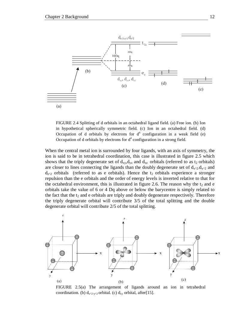
Chapter 2 Background 12
x^2-y^2 z^2
FIGURE 2.4 Splitting of d orbitals in an octahedral ligand field. (a) Free ion. (b) Ion in hypothetical spherically symmetric field. (c) Ion in an octahedral field. (d) Occupation of d orbitals by electrons for d4 configuration in a weak field (e) Occupation of d orbitals by electrons for d4 configuration in a strong field.
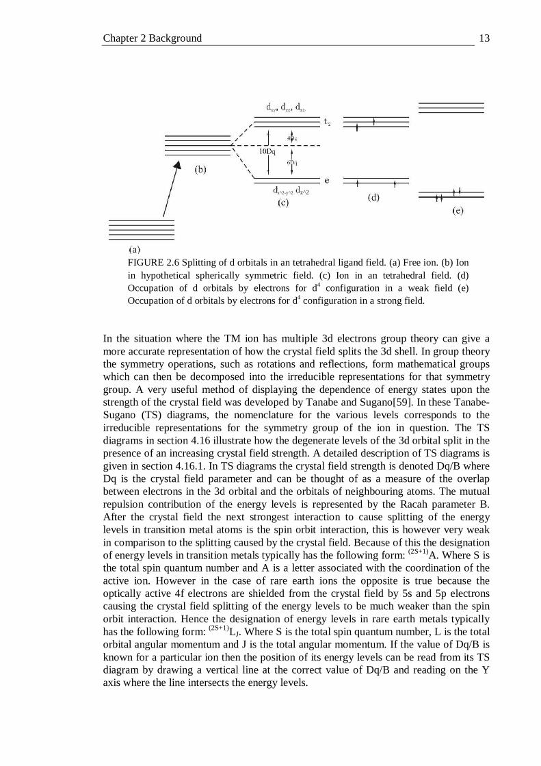
When the central metal ion is surrounded by four ligands, with an axis of symmetry, the ion is said to be in tetrahedral coordination, this case is illustrated in figure 2.5 which shows that the triply degenerate set of dxy,dyz and dxz orbitals (referred to as t2 orbitals) are closer to lines connecting the ligands than the doubly degenerate set of dx^2-dy^2 and dz^2 orbitals (referred to as e orbitals). Hence the t2 orbitals experience a stronger repulsion than the e orbitals and the order of energy levels is inverted relative to that for the octahedral environment, this is illustrated in figure 2.6. The reason why the t2 and e orbitals take the value of 6 or 4 Dq above or below the barycentre is simply related to the fact that the t2 and e orbitals are triply and doubly degenerate respectively. Therefore the triply degenerate orbital will contribute 3/5 of the total splitting and the double degenerate orbital will contribute 2/5 of the total splitting.
FIGURE 2.5(a) The arrangement of ligands around an ion in tetrahedral coordination. (b) dx^2-y^2 orbital. (c) dxy orbital, after[15].
Chapter 2 Background 13
x^2-y^2 z^2
FIGURE 2.6 Splitting of d orbitals in an tetrahedral ligand field. (a) Free ion. (b) Ion in hypothetical spherically symmetric field. (c) Ion in an tetrahedral field. (d) Occupation of d orbitals by electrons for d4 configuration in a weak field (e) Occupation of d orbitals by electrons for d4 configuration in a strong field.
In the situation where the TM ion has multiple 3d electrons group theory can give a more accurate representation of how the crystal field splits the 3d shell. In group theory the symmetry operations, such as rotations and reflections, form mathematical groups which can then be decomposed into the irreducible representations for that symmetry group. A very useful method of displaying the dependence of energy states upon the strength of the crystal field was developed by Tanabe and Sugano[59]. In these Tanabe-Sugano (TS) diagrams, the nomenclature for the various levels corresponds to the irreducible representations for the symmetry group of the ion in question. The TS diagrams in section 4.16 illustrate how the degenerate levels of the 3d orbital split in the presence of an increasing crystal field strength. A detailed description of TS diagrams is given in section 4.16.1. In TS diagrams the crystal field strength is denoted Dq/B where Dq is the crystal field parameter and can be thought of as a measure of the overlap between electrons in the 3d orbital and the orbitals of neighbouring atoms. The mutual repulsion contribution of the energy levels is represented by the Racah parameter B. After the crystal field the next strongest interaction to cause splitting of the energy levels in transition metal atoms is the spin orbit interaction, this is however very weak in comparison to the splitting caused by the crystal field. Because of this the designation of energy levels in transition metals typically has the following form: (2S+1)A. Where S is the total spin quantum number and A is a letter associated with the coordination of the active ion. However in the case of rare earth ions the opposite is true because the optically active 4f electrons are shielded from the crystal field by 5s and 5p electrons causing the crystal field splitting of the energy levels to be much weaker than the spin orbit interaction. Hence the designation of energy levels in rare earth metals typically has the following form: (2S+1)LJ. Where S is the total spin quantum number, L is the total orbital angular momentum and J is the total angular momentum. If the value of Dq/B is known for a particular ion then the position of its energy levels can be read from its TS diagram by drawing a vertical line at the correct value of Dq/B and reading on the Y axis where the line intersects the energy levels.
Chapter 2 Background 14
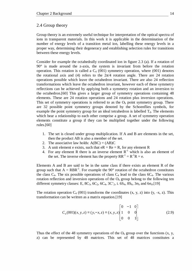
2.4 Group theory Group theory is an extremely useful technique for interpretation of the optical spectra of ions in transparent materials. In this work it is applicable in the determination of the number of energy levels of a transition metal ion, labelling these energy levels in a proper way, determining their degeneracy and establishing selection rules for transitions between these energy levels. Consider for example the octahedrally coordinated ion in figure 2.3 (a). If a rotation of 90° is made around the z-axis, the system is invariant from before the rotation operation. This rotation is called a C4 (001) symmetry operation, where (001) denotes the rotational axis and (4) refers to the 2π/4 rotation angle. There are 24 rotation operations possible which leave the octahedron invariant. There are also 24 reflection transformations which leave the octahedron invariant, however each of these symmetry reflections can be achieved by applying both a symmetry rotation and an inversion to the octahedron.[60] This gives a larger group of symmetry operations containing 48 elements. These are 24 rotation operations and 24 rotation plus inversion operations. This set of symmetry operations is referred to as the Oh point symmetry group. There are 32 possible point symmetry groups denoted by the Schoenflies symbols, for example the point symmetry group for an ideal tetrahedron is labelled Td. The elements which bear a relationship to each other comprise a group. A set of symmetry operation elements constitute a group if they can be multiplied together under the following rules.[60]
1. The set is closed under group multiplication. If A and B are elements in the set, then the product AB is also a member of the set.
2. The associative law holds: A(BC) = (AB)C 3. A unit element e exists, such that eR = Re = R, for any element R 4. For any element R there is an inverse element R-1 which is also an element of
the set. The inverse element has the property RR-1 = R-1R = e. Elements A and B are said to be in the same class if there exists an element R of the group such that A = RBR-1. For example the 90° rotation of the octahedron constitutes the class C4. The six possible operations of class C4 lead to the class 6C4. The various rotation reflection and inversion operations of the Oh group belong to the following ten different symmetry classes: E, 8C3, 6C2, 6C4, 3C’2, i. 6S4, 8S6, 3σh and 6σd.[19] The rotation operation C4 (001) transforms the coordinates (x, y, z) into (y, -x, z). This transformation can be written as a matrix equation.[19]
−=−=
100
001
010
),,(),,(),,)(001(4 zyxzxyzyxC (2.9)
Thus the effect of the 48 symmetry operations of the Oh group over the functions (x, y, z) can be represented by 48 matrices. This set of 48 matrices constitutes a
Chapter 2 Background 15
representation, and the basic functions x, y, and z are called basis functions. Each set of orthonormal basis functions φi generates a representation Γ such that
∑ Γ=j
jiji RR )(φφ (2.10)
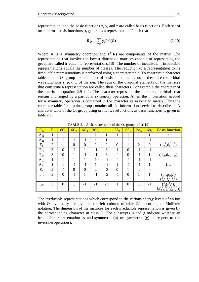
Where R is a symmetry operation and Γji(R) are components of the matrix. The representation that involve the lowest dimension matrices capable of representing the group are called irreducible representations.[19] The number of inequivalent irreducible representations equals the number of classes. The reduction of a representation to its irreducible representations is performed using a character table. To construct a character table for the Oh group a suitable set of basis functions are used, these are the orbital wavefunctions s, p, d… of the ion. The sum of the diagonal elements of the matrices that constitute a representation are called their characters. For example the character of the matrix in equation 2.9 is 1. The character represents the number of orbitals that remain unchanged by a particular symmetry operation. All of the information needed for a symmetry operation is contained in the character its associated matrix. Thus the character table for a point group contains all the information needed to describe it. A character table of the Oh group using orbital wavefunctions as basis functions is given in table 2.1.
TABLE 2.1 A character table of the Oh group, after[19].
Oh E 8C3 6C2 6C4 3C’2 i. 6S4 8S6 3σh 6σd Basis function A1g 1 1 1 1 1 1 1 1 1 1 s A2g 1 1 -1 -1 1 1 -1 1 1 -1 Eg 2 -1 0 0 2 2 0 -1 2 0 (dz
2,dx2-y
2) T1g 3 0 -1 1 -1 3 1 0 -1 -1 T2g 3 0 1 -1 -1 3 -1 0 -1 1 (dxz,dyz,dxy) A1u 1 1 1 1 1 -1 -1 -1 -1 -1 A2u 1 1 -1 -1 1 -1 1 -1 -1 1 fxyz Eu 2 -1 0 0 2 -2 0 1 -2 0 T1u 3 0 -1 1 -1 -3 -1 0 1 1 (px,py,pz)
(fx3,fy
3,fz3)
T2u 3 0 1 -1 -1 -3 1 0 1 -1 (fx(y2z2),
fy(z2x2),fz(x
2y2))
The irreducible representations which correspond to the various energy levels of an ion with Oh symmetry are given in the left column of table 2.1 according to Mulliken notation. The dimension of the matrices for each irreducible representation is given by the corresponding character in class E. The subscripts u and g indicate whether an irreducible representation is anti-symmetric (u) or symmetric (g) in respect to the inversion operation i.
Chapter 2 Background 16
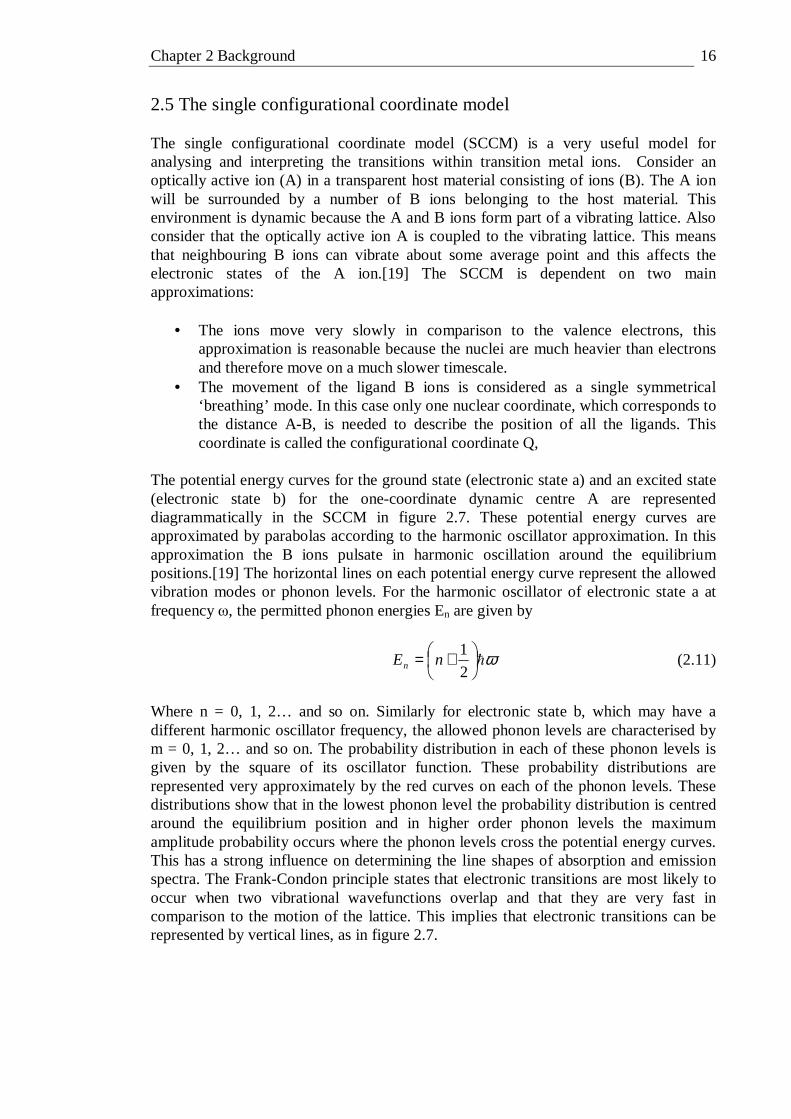
2.5 The single configurational coordinate model The single configurational coordinate model (SCCM) is a very useful model for analysing and interpreting the transitions within transition metal ions. Consider an optically active ion (A) in a transparent host material consisting of ions (B). The A ion will be surrounded by a number of B ions belonging to the host material. This environment is dynamic because the A and B ions form part of a vibrating lattice. Also consider that the optically active ion A is coupled to the vibrating lattice. This means that neighbouring B ions can vibrate about some average point and this affects the electronic states of the A ion.[19] The SCCM is dependent on two main approximations:
• The ions move very slowly in comparison to the valence electrons, this approximation is reasonable because the nuclei are much heavier than electrons and therefore move on a much slower timescale.
• The movement of the ligand B ions is considered as a single symmetrical ‘breathing’ mode. In this case only one nuclear coordinate, which corresponds to the distance A-B, is needed to describe the position of all the ligands. This coordinate is called the configurational coordinate Q,
The potential energy curves for the ground state (electronic state a) and an excited state (electronic state b) for the one-coordinate dynamic centre A are represented diagrammatically in the SCCM in figure 2.7. These potential energy curves are approximated by parabolas according to the harmonic oscillator approximation. In this approximation the B ions pulsate in harmonic oscillation around the equilibrium positions.[19] The horizontal lines on each potential energy curve represent the allowed vibration modes or phonon levels. For the harmonic oscillator of electronic state a at frequency ω, the permitted phonon energies En are given by
ωh
+=2
1nEn (2.11)
Where n = 0, 1, 2… and so on. Similarly for electronic state b, which may have a different harmonic oscillator frequency, the allowed phonon levels are characterised by m = 0, 1, 2… and so on. The probability distribution in each of these phonon levels is given by the square of its oscillator function. These probability distributions are represented very approximately by the red curves on each of the phonon levels. These distributions show that in the lowest phonon level the probability distribution is centred around the equilibrium position and in higher order phonon levels the maximum amplitude probability occurs where the phonon levels cross the potential energy curves. This has a strong influence on determining the line shapes of absorption and emission spectra. The Frank-Condon principle states that electronic transitions are most likely to occur when two vibrational wavefunctions overlap and that they are very fast in comparison to the motion of the lattice. This implies that electronic transitions can be represented by vertical lines, as in figure 2.7.
Chapter 2 Background 17
FIGURE 2.7 The single configurational coordinate model, showing how phonon assisted absorption gives rise to absorption line shapes and the mechanisms for phonon assisted non-radiative decay.
The peak in the absorption band occurs at an energy where the overlap between the probability distribution in the phonon levels is at a maximum, which is illustrated in figure 2.7 by the transition Ea. Similarly the peak in the emission band corresponds to the transition Ee. The difference between the absorption and emission peaks (Ea - Ee) is known as the Stokes shift (SS), i.e. SS = Ea - Ee. It should be noted that the equilibrium position coordinates Q0
a and Q0b are different for the electronic states a and b. This
reflects the difference in electron-phonon coupling between the two states. The dimensionless Huang-Rhys parameter (S) quantifies this difference in electron-phonon coupling and is given by
ωhdisE
S = (2.12)
Where Edis is defined in figure 2.7 and ħω is the energy of the breathing mode vibration. The Huang-Rhys parameter is related to the Stokes shift by
ωh)12( −=−= SEESS ea (2.13)
Chapter 2 Background 18
The absorption band shape, induced from phenomena illustrated in the SCCM in figure 2.7, is due to overlapping occurring between the vibrational m states and the n = 0 phonon level, which would occur at very low temperatures (~0 K). The transitions n = 0 ↔ m = 0 are termed zero phonon lines (ZPL) as they occur without the participation of phonons. ZPL are characterised by relatively narrow line-widths which, disregarding the effect of the host, is the natural linewidth discussed in section 2.6.1. These transitions can commonly be observed in the low temperature absorption and emission spectra of transition metal doped crystals, as in V2+ doped ZnSe for example.[61] However they are rarely observed in transition metal doped glasses because of the greater inhomogeneous broadening in these hosts. It can be seen from figure 2.7 that for sufficient S no ZPL will be observed. Once in an excited state, the ion A can reach its ground state through the emission of a photon (radiative decay) or through the emission of phonons (non-radiative decay). Non-radiative decay can be accounted for by the SCCM, illustrated in figure 2.7. For sufficiently large S, excitation from the ground state results in the population of higher order phonon modes in the excited state. These higher order phonon modes can coincide with the crossing of the potential energy curves of excited state a and b and therefore the system can relax through the phonon levels of excited state a. If the populated higher order phonon modes coincides with the proximity of the potential energy curves of excited state a and b then the same process may occur by tunnelling. 2.6 Broadening mechanisms The SCCM shows how various absorption and emission lines are generated from the overlap between probability distributions in phonon levels of the ground and excited state. In a real system these absorption and emission line are usually broadened further. The mechanisms responsible for this broadening can be categorised as either homogeneous or inhomogeneous. 2.6.1 Homogeneous broadening Homogeneous broadening is an increase in absorption and emission linewidth caused by phenomena that influence each ion equally. The most fundamental of the homogeneous broadening mechanisms is the natural, or minimum, linewidth. This arises from the Heisenberg uncertainty principle which states that the uncertainty in determining the energy width ∆E of an energy level that has a minimum uncertainty in its lifetime ∆t, is obtained from the relationship ∆E = ħ/ ∆t.[56] Another type of homogeneous broadening is caused by collisions between phonons and optically active ions. These collisions can cause a decrease in decay lifetime when the phonons “knock” an electron from the excited state before it has the opportunity to radiate spontaneously.[56] Dephasing collisions between phonons and optically active ions can also occur; these collisions interrupt the phase of radiating ions without increasing their population decay rate. Consequently temporal coherence is reduced and the emission linewidth is broadened.[23]
Chapter 2 Background 19
2.6.2 Inhomogeneous broadening Inhomogeneous broadening arises from the range of local environments experienced by different ions. This range of local field environments is the manifestation of a variety of crystal field strengths, coordination number, symmetry and proximity to defects. Crystal hosts have a relatively ordered structure; therefore inhomogeneous broadening is relatively weak and arises principally from defects and strains in the crystal. In glass hosts inhomogeneous broadening is relatively strong which causes the absorption and emission spectra of ions in glass hosts to have characteristic broad linewidths. This strong inhomogeneous broadening is related to a fundamental characteristic of glasses, this is their disordered structure. Inhomogeneous broadening results in the superposition of a range of homogeneously broadened lines which generates the observed absorption and emission spectra of an ion. 2.7 Selection rules Since electric dipole processes dominate over magnetic dipole transition strength, magnetic dipole transitions are neglected in this discussion. For electric dipole interaction the rules for allowed transition are:[60]
• No change in spin, i.e. ∆S=0 • The change in angular momentum ∆L is ±1 • The change in total momentum ∆J is 0, ±1, but not J = 0 → J = 0 • No change in parity
Radiative transitions in the transition metal ions involve electrons in the same 3dn configuration, electric dipole transitions are not allowed between these equal parity states and mixing of the higher lying 4p odd parity states is required for electric dipole transitions to occur. The mixing of different parity states is permitted when inversion symmetry of the crystal field is broken, either by an asymmetric distribution of ligands around the ion or a distortion of the symmetry by odd parity phonons. Electric dipole transitions, due to mixing by odd-parity phonons, are called vibronic transitions and are more common in transition metals than rare earths because of the stronger electron-lattice coupling.[62] 2.8 Structure of GLS This section gives a brief general description of the structure of glass, some structural phenomenon relevant to chalcogenide glasses and some structural properties of GLS glass relevant to the discussion in section 4.7. 2.8.1 General structure of glass Glasses can be thought of as having a disordered structure since unlike crystals they do not have long range order. However, there is usually short range order present in that each constituent ion has a specific number of ligands. This description of glasses forms the basis of the continuous random network model, first proposed by Zachariasen in 1932.[63] Constituents of glass are generally divided into two broad categories: network
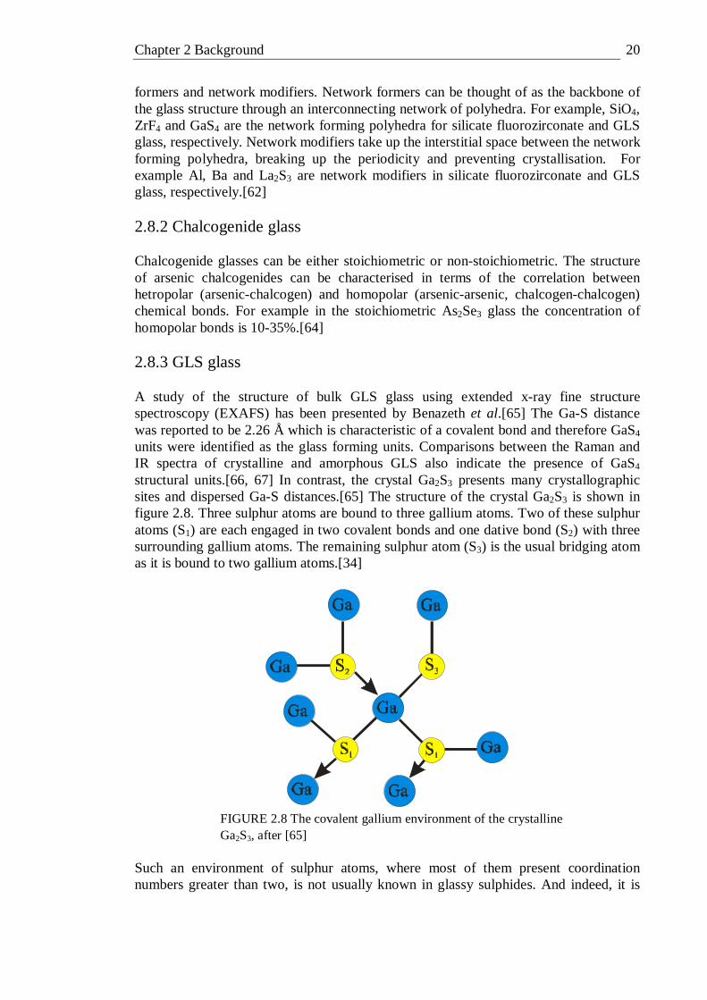
Chapter 2 Background 20
formers and network modifiers. Network formers can be thought of as the backbone of the glass structure through an interconnecting network of polyhedra. For example, SiO4, ZrF4 and GaS4 are the network forming polyhedra for silicate fluorozirconate and GLS glass, respectively. Network modifiers take up the interstitial space between the network forming polyhedra, breaking up the periodicity and preventing crystallisation. For example Al, Ba and La2S3 are network modifiers in silicate fluorozirconate and GLS glass, respectively.[62] 2.8.2 Chalcogenide glass Chalcogenide glasses can be either stoichiometric or non-stoichiometric. The structure of arsenic chalcogenides can be characterised in terms of the correlation between hetropolar (arsenic-chalcogen) and homopolar (arsenic-arsenic, chalcogen-chalcogen) chemical bonds. For example in the stoichiometric As2Se3 glass the concentration of homopolar bonds is 10-35%.[64] 2.8.3 GLS glass A study of the structure of bulk GLS glass using extended x-ray fine structure spectroscopy (EXAFS) has been presented by Benazeth et al.[65] The Ga-S distance was reported to be 2.26 Å which is characteristic of a covalent bond and therefore GaS4 units were identified as the glass forming units. Comparisons between the Raman and IR spectra of crystalline and amorphous GLS also indicate the presence of GaS4 structural units.[66, 67] In contrast, the crystal Ga2S3 presents many crystallographic sites and dispersed Ga-S distances.[65] The structure of the crystal Ga2S3 is shown in figure 2.8. Three sulphur atoms are bound to three gallium atoms. Two of these sulphur atoms (S1) are each engaged in two covalent bonds and one dative bond (S2) with three surrounding gallium atoms. The remaining sulphur atom (S3) is the usual bridging atom as it is bound to two gallium atoms.[34]
FIGURE 2.8 The covalent gallium environment of the crystalline Ga2S3, after [65]
Such an environment of sulphur atoms, where most of them present coordination numbers greater than two, is not usually known in glassy sulphides. And indeed, it is
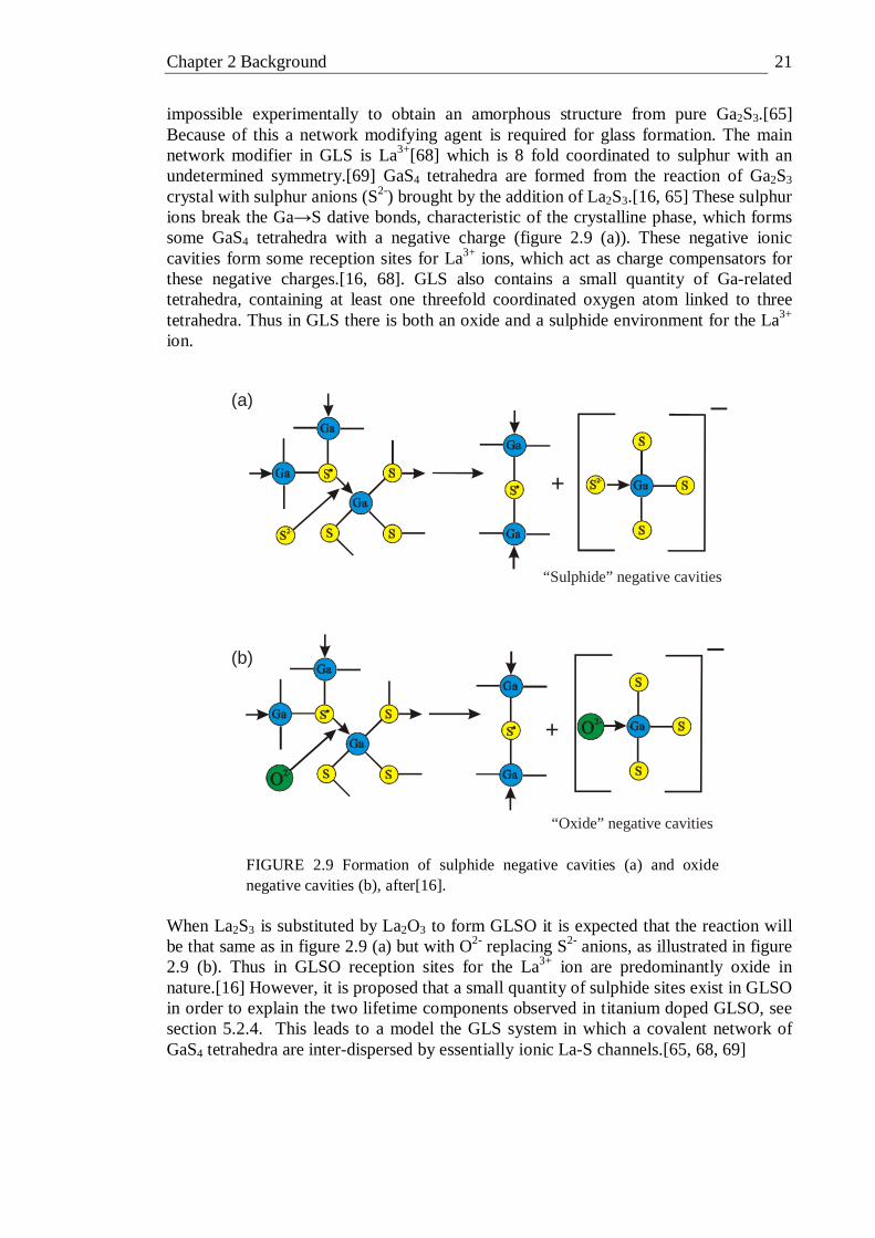
Chapter 2 Background 21
impossible experimentally to obtain an amorphous structure from pure Ga2S3.[65] Because of this a network modifying agent is required for glass formation. The main network modifier in GLS is La3+[68] which is 8 fold coordinated to sulphur with an undetermined symmetry.[69] GaS4 tetrahedra are formed from the reaction of Ga2S3 crystal with sulphur anions (S2-) brought by the addition of La2S3.[16, 65] These sulphur ions break the Ga→S dative bonds, characteristic of the crystalline phase, which forms some GaS4 tetrahedra with a negative charge (figure 2.9 (a)). These negative ionic cavities form some reception sites for La3+ ions, which act as charge compensators for these negative charges.[16, 68]. GLS also contains a small quantity of Ga-related tetrahedra, containing at least one threefold coordinated oxygen atom linked to three tetrahedra. Thus in GLS there is both an oxide and a sulphide environment for the La3+ ion.
“Sulphide” negative cavities
“Oxide” negative cavities
(a)
(b)
+
+
FIGURE 2.9 Formation of sulphide negative cavities (a) and oxide negative cavities (b), after[16].
When La2S3 is substituted by La2O3 to form GLSO it is expected that the reaction will be that same as in figure 2.9 (a) but with O2- replacing S2- anions, as illustrated in figure 2.9 (b). Thus in GLSO reception sites for the La3+ ion are predominantly oxide in nature.[16] However, it is proposed that a small quantity of sulphide sites exist in GLSO in order to explain the two lifetime components observed in titanium doped GLSO, see section 5.2.4. This leads to a model the GLS system in which a covalent network of GaS4 tetrahedra are inter-dispersed by essentially ionic La-S channels.[65, 68, 69]

Chapter 3 Glass melting and spectroscopic techniques 22
Chapter 3
Glass melting and spectroscopic techniques 3.1 Introduction The first part of this chapter details the melting procedures for the fabrication of transition metal doped GLS, in particular, vanadium doped GLS. Other authors, notably Mairaj[34] and Brady,[70] have carried out a very exhaustive analysis of the raw material purification and glass melting procedures for GLS. The fabrication of transition metal doped samples examined in this work used many of the techniques developed by Mairaj and Brady without further enhancement; these techniques are therefore only briefly summarised. Detailed in this chapter are melting procedures developed for the fabrication of low doping concentration transition metal doped GLS glass. The second part of this chapter details all of the spectroscopic techniques used in the analysis of transition metal doped GLS in sufficient detail for the reader to understand, critique and repeat them. A brief introduction to each spectroscopic technique is given. Absorption, Raman, XPS and EPR measurements were taken on commercially manufactured equipment since they were available with the required specifications. The lack of commercially manufactured equipment with the required specifications for photoluminescence, excitation, lifetime and quantum efficiency measurements meant they were taken on in house equipment. The in house equipment may not have been able to compete with commercially manufactured versions, were they available, in repeatability but they did allow a degree of functionality and specialisation not possible with a manufactured system. 3.2 Glass melting procedures 3.2.1 Batching and melting details of transition metal doped GLS samples Raw material purity is particularly important for the synthesis of GLS glass, as ion concentrations as low as 1ppm can result in strong absorption signatures.[70] Hydroxyl impurities are also detrimental to the optical transmission of GLS and the quantum efficiency of doped samples; to that end water needs to be eliminated both from the raw material and the synthesis process as much as possible. The precursor materials required for the production of GLS glass are: gallium sulphide GaxSy (this comes in three phases GaS, Ga2S3 and Ga4S5) lanthanum sulphide La2S3, and lanthanum oxide La2O3. These melt materials are not available from any supplier at the desired purity, however their precursors (gallium metal, lanthanum halides and gaseous hydrogen sulphide) are. So gallium and lanthanum sulphides were synthesised in-house from gallium metal (9N purity) and lanthanum fluoride (5N purity) precursors in a flowing H2S gas system. It may be possible to use chlorides as precursors but researches who developed the GLS fabrication process[34, 70] chose to use gallium metal and lanthanum fluoride because they were the highest purity precursors available. The flowing system sweeps the by-products of the reaction out of the hot zone, preventing them from reacting, and by Le Chatelier’s principle shifting the position of equilibrium to (as much as 100%) favour the sulphurised product.[34] This principle can be illustrated by imagining the reaction
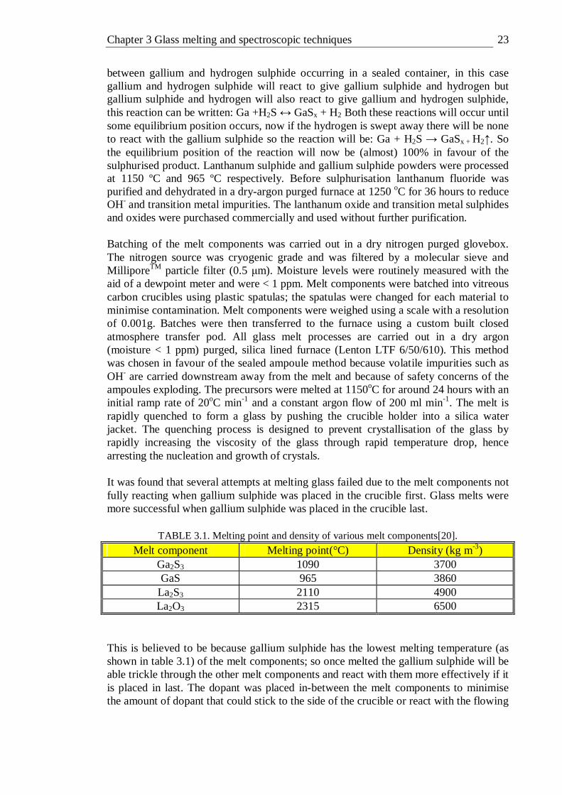
Chapter 3 Glass melting and spectroscopic techniques 23
between gallium and hydrogen sulphide occurring in a sealed container, in this case gallium and hydrogen sulphide will react to give gallium sulphide and hydrogen but gallium sulphide and hydrogen will also react to give gallium and hydrogen sulphide, this reaction can be written: Ga +H2S ↔ GaSx + H2 Both these reactions will occur until some equilibrium position occurs, now if the hydrogen is swept away there will be none to react with the gallium sulphide so the reaction will be: Ga + H2S → GaSx + H2↑. So the equilibrium position of the reaction will now be (almost) 100% in favour of the sulphurised product. Lanthanum sulphide and gallium sulphide powders were processed at 1150 ºC and 965 ºC respectively. Before sulphurisation lanthanum fluoride was purified and dehydrated in a dry-argon purged furnace at 1250 oC for 36 hours to reduce OH- and transition metal impurities. The lanthanum oxide and transition metal sulphides and oxides were purchased commercially and used without further purification. Batching of the melt components was carried out in a dry nitrogen purged glovebox. The nitrogen source was cryogenic grade and was filtered by a molecular sieve and MilliporeTM particle filter (0.5 µm). Moisture levels were routinely measured with the aid of a dewpoint meter and were < 1 ppm. Melt components were batched into vitreous carbon crucibles using plastic spatulas; the spatulas were changed for each material to minimise contamination. Melt components were weighed using a scale with a resolution of 0.001g. Batches were then transferred to the furnace using a custom built closed atmosphere transfer pod. All glass melt processes are carried out in a dry argon (moisture < 1 ppm) purged, silica lined furnace (Lenton LTF 6/50/610). This method was chosen in favour of the sealed ampoule method because volatile impurities such as OH- are carried downstream away from the melt and because of safety concerns of the ampoules exploding. The precursors were melted at 1150oC for around 24 hours with an initial ramp rate of 20oC min-1 and a constant argon flow of 200 ml min-1. The melt is rapidly quenched to form a glass by pushing the crucible holder into a silica water jacket. The quenching process is designed to prevent crystallisation of the glass by rapidly increasing the viscosity of the glass through rapid temperature drop, hence arresting the nucleation and growth of crystals. It was found that several attempts at melting glass failed due to the melt components not fully reacting when gallium sulphide was placed in the crucible first. Glass melts were more successful when gallium sulphide was placed in the crucible last.
TABLE 3.1. Melting point and density of various melt components[20].
Melt component Melting point(°C) Density (kg m-3) Ga2S3 1090 3700 GaS 965 3860
La2S3 2110 4900 La2O3 2315 6500
This is believed to be because gallium sulphide has the lowest melting temperature (as shown in table 3.1) of the melt components; so once melted the gallium sulphide will be able trickle through the other melt components and react with them more effectively if it is placed in last. The dopant was placed in-between the melt components to minimise the amount of dopant that could stick to the side of the crucible or react with the flowing

Chapter 3 Glass melting and spectroscopic techniques 24
argon atmosphere of the furnace. Hence melt components were added to the crucible in the following sequence: lanthanum oxide, lanthanum sulphide, transition metal dopant then gallium sulphide. The transition metals and their compounds, that were used to dope GLS glass for this study, are detailed in table 3.2
TABLE 3.2. Transition metals dopants and their compounds. Transition metal dopant Compound Supplier Purity (%)
vanadium V2S3, V2O5 Cerac 99.8, 99.9 chromium Cr2S3 Cerac 99 titanium TiS2, Ti2S3 Johnson
Matthey 99.95
nickel NiS Cerac 99.9
iron Fe2O3 Merck 99
cobalt CoS3, CoS2 Cerac 99.5 bismuth Bi2S3 Cerac 99.9
3.2.2 Batching and melting details of vanadium doped GLS samples Because vanadium doped GLS has been studied in more detail than other transition metal dopants in this study, the fabrication process for vanadium doped GLS samples is detailed in this section. Initial samples of vanadium doped GLS were batched from the melt components in the molar percentages specified in table 3.3 the concentration of vanadium ions is also given.
TABLE 3.3. Molar percentages of melt components for initial vanadium doped GLS melts.
Melt code GaxSy (%molar)
La2S3
(%molar) La2O3
(%molar) V2S3
(% molar) Vx+
(% molar) LD1175-C 64.55 30.38 5.054 0.0083 0.015 LD1257-1 71.15 24.00 4.73 0.054 0.108 LD1257-2 69.62 23.85 6.01 0.259 0.518 LD1257-3 69.72 23.19 6.05 0.519 1.038
Given the 0.001 gram resolution of the weighing scales, which gave a molar % concentration resolution of around 0.015% for a 20 gram melt, a method was devised for giving greater control of the amount of dopant at low concentrations. To accomplish this a high doping concentration glass of around 2.5 % molar vanadium was melted first, this is referred to as the dopant glass. The dopant glass in the appropriate proportions was then re-melted with the melt components to produce low doping concentration glass. Two vanadium compounds with different oxidation states were used; V2S3 with vanadium in a 3+ oxidation state and V2O5 with vanadium in a 5+ oxidation state. This was done in order to determine if the initial oxidation state of the vanadium dopant would affect the optical properties of the glass. Copper and silver co-dopants have been shown to enhance the emission of vanadium doped CdS, ZnS CdSe and ZnSe by up to a factor of 10, this was attributed by the authors to copper and silver
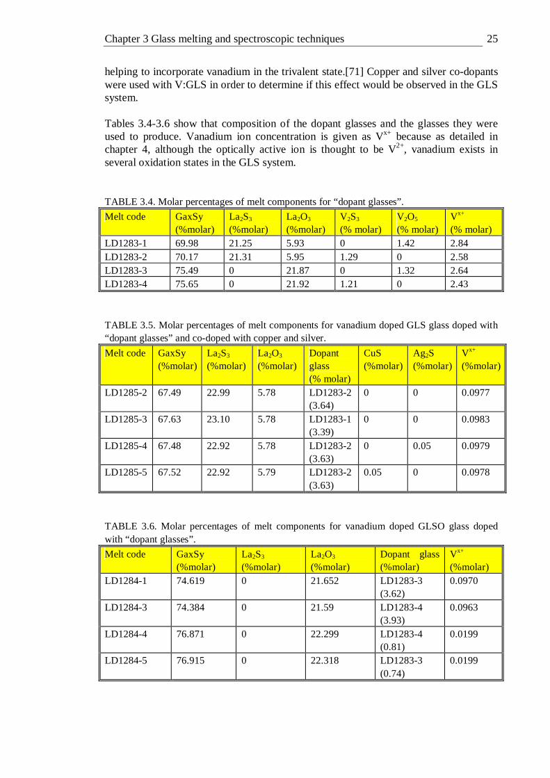
Chapter 3 Glass melting and spectroscopic techniques 25
helping to incorporate vanadium in the trivalent state.[71] Copper and silver co-dopants were used with V:GLS in order to determine if this effect would be observed in the GLS system. Tables 3.4-3.6 show that composition of the dopant glasses and the glasses they were used to produce. Vanadium ion concentration is given as Vx+ because as detailed in chapter 4, although the optically active ion is thought to be V2+, vanadium exists in several oxidation states in the GLS system. TABLE 3.4. Molar percentages of melt components for “dopant glasses”.
Melt code GaxSy (%molar)
La2S3
(%molar) La2O3
(%molar) V2S3 (% molar)
V2O5 (% molar)
Vx+ (% molar)
LD1283-1 69.98 21.25 5.93 0 1.42 2.84 LD1283-2 70.17 21.31 5.95 1.29 0 2.58 LD1283-3 75.49 0 21.87 0 1.32 2.64 LD1283-4 75.65 0 21.92 1.21 0 2.43
TABLE 3.5. Molar percentages of melt components for vanadium doped GLS glass doped with “dopant glasses” and co-doped with copper and silver.
Melt code GaxSy (%molar)
La2S3
(%molar) La2O3
(%molar) Dopant glass (% molar)
CuS (%molar)
Ag2S (%molar)
Vx+ (%molar)
LD1285-2 67.49 22.99 5.78 LD1283-2 (3.64)
0 0 0.0977
LD1285-3 67.63 23.10 5.78 LD1283-1 (3.39)
0 0 0.0983
LD1285-4 67.48 22.92 5.78 LD1283-2 (3.63)
0 0.05 0.0979
LD1285-5 67.52 22.92 5.79 LD1283-2 (3.63)
0.05 0 0.0978
TABLE 3.6. Molar percentages of melt components for vanadium doped GLSO glass doped with “dopant glasses”.
Melt code GaxSy (%molar)
La2S3
(%molar) La2O3
(%molar) Dopant glass (%molar)
Vx+ (%molar)
LD1284-1 74.619 0 21.652 LD1283-3 (3.62)
0.0970
LD1284-3 74.384 0 21.59 LD1283-4 (3.93)
0.0963
LD1284-4 76.871 0 22.299 LD1283-4 (0.81)
0.0199
LD1284-5 76.915 0 22.318 LD1283-3 (0.74)
0.0199

Chapter 3 Glass melting and spectroscopic techniques 26
3.3 Spectroscopic techniques 3.3.1 Absorption spectroscopy When the frequency of light incident on a solid is resonant with an electronic transition between two energy levels intrinsic to the material an increase in absorption is observed. Hence an absorption spectroscopy can be used to probe the energy level structure of a material
Absorption spectra were taken on a Varian Cary 500 spectrophotometer which operates over a range of 175-3300nm with a resolution of ±0.1nm in the UV-VIS region and ±0.4nm in the infrared region. A basic schematic of the optics in the Cary 500 is shown in figure 3.1; the inset shows the chopper blade. One section of the chopper is mirrored and reflects the light beam, one section of the chopper is cut-out and allows the light beam to pass, and one section is matt black. This allows light to be directed alternately to the sample and reference beams. The matt black section of the chopper allows the grating to move to the next wavelength and enables correction for dark current. The system then compares the intensity of monochromatic light transmitted through the sample with the reference beam, 100% transmission and zero corrections are taken to account for system response and dark noise. Samples were held vertically in a V groove against an aperture 3mm in diameter, the reference beam also passed through an aperture 3mm in diameter.
FIGURE 3.1 Basic schematic of the optics in the Varian Cary 500 spectrophotometer.

Chapter 3 Glass melting and spectroscopic techniques 27
The Cary 500 uses two gratings to produce monochromatic light: a 1200 line/mm grating which is used when scanning 175 - 800 nm and a 300 line/mm grating which is used when scanning 800 – 3300 nm. Two lamps are available: a deuterium lamp (below 350 nm) and a tungsten halogen lamp (above 350 nm). The detectors used are a photomultiplier tube (below 800 nm) and a thermoelectric cooled PbS detector (above 800 nm). The change of grating and detector at 800 nm causes a small but sudden increase in transmission at 800 nm that was not always fully corrected for by the background scan. To overcome this, the increase in transmission observed was subtracted from wavelengths > 800 nm. Samples that were cut and polished into thick and thin samples with thicknesses of l1 and l2 allowed reflection corrected absorption coefficient spectra to be calculated using equation 3.1.
21
)()()( 21
ll
AAa
llrc −
−=
λλλ (3.1)
Where arc(λ) is the reflection corrected absorption coefficient spectrum and )(λ
ilA is the
absorbance spectra of a sample of thickness li. 3.3.2 Photoluminescence spectroscopy Similarly to absorption, photoluminescence can be used to probe the energy level structure of a material, however in the case of photoluminescence light is absorbed by the material (usually at one wavelength) exciting electrons (usually from the ground state) into higher energy levels. The electrons then relax back down to the ground state in a spin-allowed transition, called fluorescence, or in a spin-forbidden transition, called phosphorescence. Photoluminescence spectra were taken with the equipment setup illustrated in figure 3.2.
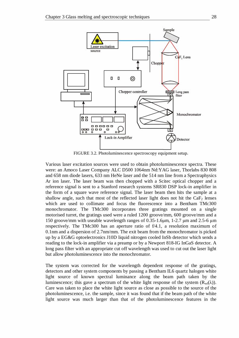
Chapter 3 Glass melting and spectroscopic techniques 28
FIGURE 3.2. Photoluminescence spectroscopy equipment setup.
Various laser excitation sources were used to obtain photoluminescence spectra. These were: an Amoco Laser Company ALC D500 1064nm Nd:YAG laser, Thorlabs 830 808 and 658 nm diode lasers, 633 nm HeNe laser and the 514 nm line from a Spectraphysics Ar ion laser. The laser beam was then chopped with a Scitec optical chopper and a reference signal is sent to a Stanford research systems SR830 DSP lock-in amplifier in the form of a square wave reference signal. The laser beam then hits the sample at a shallow angle, such that most of the reflected laser light does not hit the CaF2 lenses which are used to collimate and focus the fluorescence into a Bentham TMc300 monochromator. The TMc300 incorporates three gratings mounted on a single motorised turret, the gratings used were a ruled 1200 groove/mm, 600 groove/mm and a 150 groove/mm with useable wavelength ranges of 0.35-1.6µm, 1-2.7 µm and 2.5-6 µm respectively. The TMc300 has an aperture ratio of f/4.1, a resolution maximum of 0.1nm and a dispersion of 2.7nm/mm. The exit beam from the monochromator is picked up by a EG&G optoelectronics J10D liquid nitrogen cooled InSb detector which sends a reading to the lock-in amplifier via a preamp or by a Newport 818-IG InGaS detector. A long pass filter with an appropriate cut off wavelength was used to cut out the laser light but allow photoluminescence into the monochromator. The system was corrected for the wavelength dependent response of the gratings, detectors and other system components by passing a Bentham IL6 quartz halogen white light source of known spectral luminance along the beam path taken by the luminescence; this gave a spectrum of the white light response of the system (Rwl(λ)). Care was taken to place the white light source as close as possible to the source of the photoluminescence, i.e. the sample, since it was found that if the beam path of the white light source was much larger than that of the photoluminescence features in the
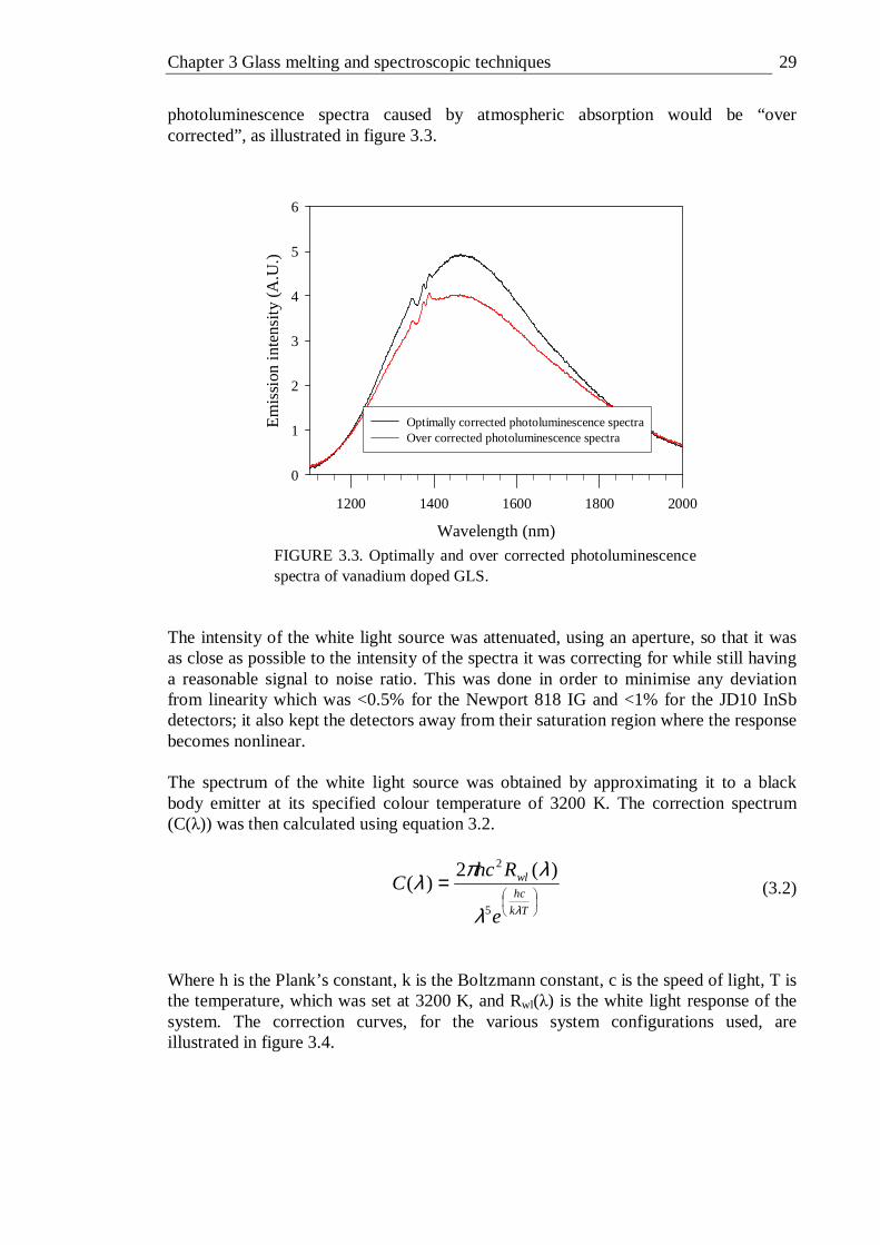
Chapter 3 Glass melting and spectroscopic techniques 29
photoluminescence spectra caused by atmospheric absorption would be “over corrected”, as illustrated in figure 3.3.
Wavelength (nm)
1200 1400 1600 1800 2000
Em
issi
on in
ten
sity
(A
.U.)
0
1
2
3
4
5
6
Optimally corrected photoluminescence spectraOver corrected photoluminescence spectra
FIGURE 3.3. Optimally and over corrected photoluminescence spectra of vanadium doped GLS.
The intensity of the white light source was attenuated, using an aperture, so that it was as close as possible to the intensity of the spectra it was correcting for while still having a reasonable signal to noise ratio. This was done in order to minimise any deviation from linearity which was <0.5% for the Newport 818 IG and <1% for the JD10 InSb detectors; it also kept the detectors away from their saturation region where the response becomes nonlinear. The spectrum of the white light source was obtained by approximating it to a black body emitter at its specified colour temperature of 3200 K. The correction spectrum (C(λ)) was then calculated using equation 3.2.
=
Tk
hc
wl
e
RhcC
λλ
λπλ5
2 )(2)( (3.2)
Where h is the Plank’s constant, k is the Boltzmann constant, c is the speed of light, T is the temperature, which was set at 3200 K, and Rwl(λ) is the white light response of the system. The correction curves, for the various system configurations used, are illustrated in figure 3.4.
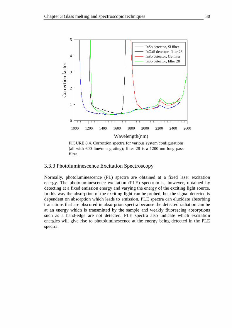
Chapter 3 Glass melting and spectroscopic techniques 30
Wavelength(nm)
1000 1200 1400 1600 1800 2000 2200 2400 2600
Cor
rect
ion
fact
or
0
1
2
3
4
5
InSb detector, Si filterInGaS detector, filter 28 InSb detector, Ge filter InSb detector, filter 28
FIGURE 3.4. Correction spectra for various system configurations (all with 600 line/mm grating); filter 28 is a 1200 nm long pass filter.
3.3.3 Photoluminescence Excitation Spectroscopy Normally, photoluminescence (PL) spectra are obtained at a fixed laser excitation energy. The photoluminescence excitation (PLE) spectrum is, however, obtained by detecting at a fixed emission energy and varying the energy of the exciting light source. In this way the absorption of the exciting light can be probed, but the signal detected is dependent on absorption which leads to emission. PLE spectra can elucidate absorbing transitions that are obscured in absorption spectra because the detected radiation can be at an energy which is transmitted by the sample and weakly fluorescing absorptions such as a band-edge are not detected. PLE spectra also indicate which excitation energies will give rise to photoluminescence at the energy being detected in the PLE spectra.
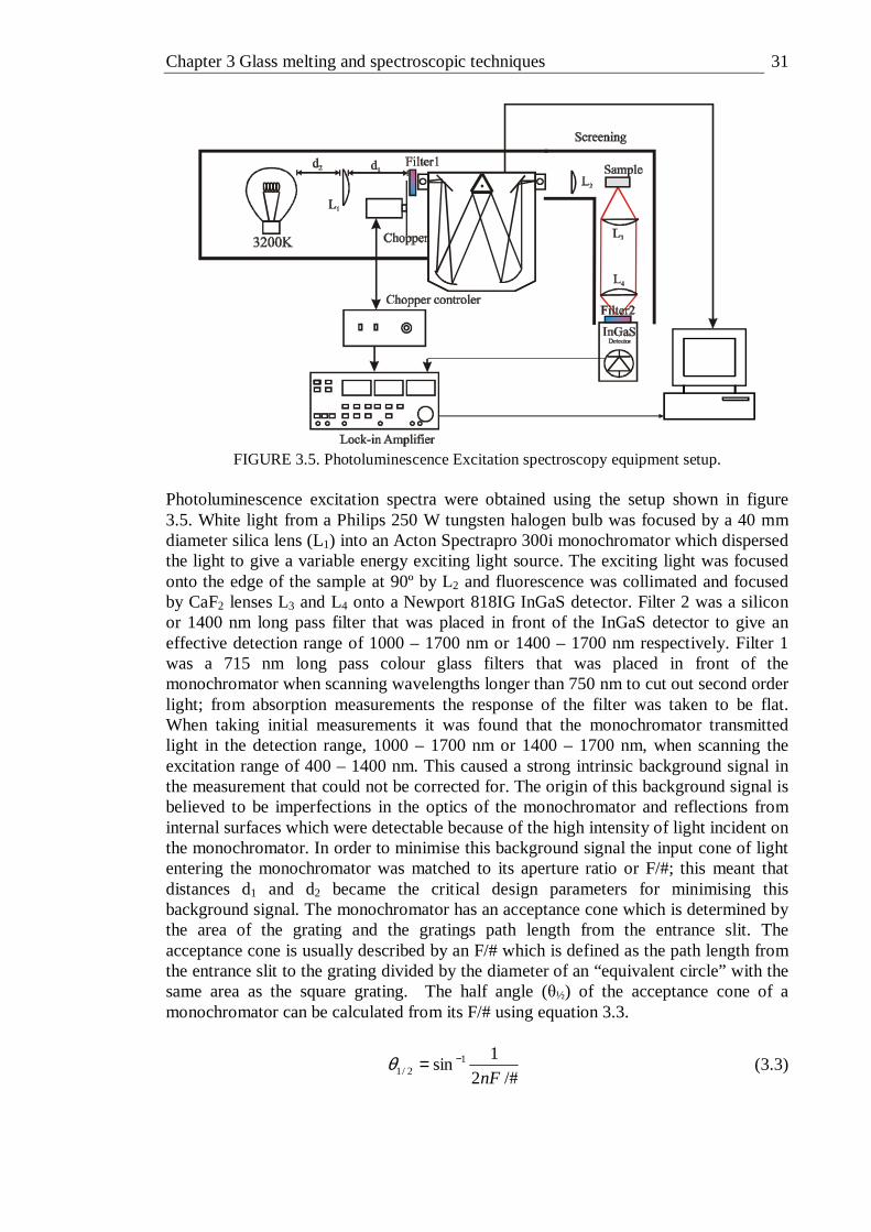
Chapter 3 Glass melting and spectroscopic techniques 31
FIGURE 3.5. Photoluminescence Excitation spectroscopy equipment setup.
Photoluminescence excitation spectra were obtained using the setup shown in figure 3.5. White light from a Philips 250 W tungsten halogen bulb was focused by a 40 mm diameter silica lens (L1) into an Acton Spectrapro 300i monochromator which dispersed the light to give a variable energy exciting light source. The exciting light was focused onto the edge of the sample at 90º by L2 and fluorescence was collimated and focused by CaF2 lenses L3 and L4 onto a Newport 818IG InGaS detector. Filter 2 was a silicon or 1400 nm long pass filter that was placed in front of the InGaS detector to give an effective detection range of 1000 – 1700 nm or 1400 – 1700 nm respectively. Filter 1 was a 715 nm long pass colour glass filters that was placed in front of the monochromator when scanning wavelengths longer than 750 nm to cut out second order light; from absorption measurements the response of the filter was taken to be flat. When taking initial measurements it was found that the monochromator transmitted light in the detection range, 1000 – 1700 nm or 1400 – 1700 nm, when scanning the excitation range of 400 – 1400 nm. This caused a strong intrinsic background signal in the measurement that could not be corrected for. The origin of this background signal is believed to be imperfections in the optics of the monochromator and reflections from internal surfaces which were detectable because of the high intensity of light incident on the monochromator. In order to minimise this background signal the input cone of light entering the monochromator was matched to its aperture ratio or F/#; this meant that distances d1 and d2 became the critical design parameters for minimising this background signal. The monochromator has an acceptance cone which is determined by the area of the grating and the gratings path length from the entrance slit. The acceptance cone is usually described by an F/# which is defined as the path length from the entrance slit to the grating divided by the diameter of an “equivalent circle” with the same area as the square grating. The half angle (θ½) of the acceptance cone of a monochromator can be calculated from its F/# using equation 3.3.
/#2
1sin 1
2/1 nF−=θ (3.3)

Chapter 3 Glass melting and spectroscopic techniques 32
Where n is the order of diffraction. The Acton Spectrapro 300i has a F/# of 4 from which a θ½ of 7.2° was calculated. Adjusting d1 to give θ½ = 7.2° still resulted in interference. In order to optimise the system experimentally, the setup shown in figure 3.6 was arranged. The monochromator was fixed at 590 nm this wavelength was detected by a Newport 818-SL silicon photo-diode from a reflection off a microscope slide, to give the intensity of the excitation (Iex) . The background signal (Iback) was detected by a Newport 818IG InGaS detector fronted by a silicon filter; d1 and d2 were then varied to maximise Iex/Iback. The optimal setting for d1 and d2 was found to be 250 and 350 mm respectively; this corresponded to θ½ and F/# of 4.6° and 6.3 respectively. The reason why the interference was minimised when the acceptance cone is under-filled may be because the specified F/# for the monochromator is calculated for an equivalent circle which would have sections of light missing the grating.
FIGURE 3.6. Experimental setup for optimisation of system interference.
Another source of interference was found to be scattered chopped white light that was detected by the detector which was in free space. To minimise this, black card screening was erected around the optics. The PLE system was corrected for the varying intensity of exciting light, due to varying grating response and spectral output of the white light source, by obtaining the white light response ((Rwl(λ)) for each grating with Newport 818-SL and 818-IG detectors. The correction curves for each grating were then calculated using the calibration report supplied with the detectors. The calibration reports gave the responsivity of the detectors in steps of 10 nm. The spectral responsivity data was entered onto a computer and smoothed with a running average algorithm, with a sampling proportion of 0.05, to give detector responsivity spectra (Rdet(λ)) in steps of 1 nm. The correction spectra (C(λ)) for each grating were then calculated using equation 3.4. The grating correction spectra are given in figure 3.7.
)(
)()(
det λλλ
R
RC wl= (3.4)

Chapter 3 Glass melting and spectroscopic techniques 33
Wavelength (nm)
400 500 600 700 800 900 1000 1100 1200 1300 1400 1500 1600
Cor
rect
ion
fa
cto
r (A
.U.)
0.0
0.1
0.2
0.3
0.4
0.5
600 lines/mm blazed grating 1200 lines/mm blazed grating
FIGURE 3.7. Correction spectra for gratings used in PLE measurements.
In order to test if the PLE system would give valid results, a sample of neodymium doped GLS was scanned. The results are shown in figure 3.8, along with the absorption of neodymium GLS; as expected for a valid scan the PLE peaks match the absorption peaks. Note that an absorption band centred at 540 nm, that could not be clearly identified in the absorption spectrum because of its proximity to the band-edge, has been elucidated in the PLE spectra. This is because the PLE system detects emission from incident light at a wavelength that is transmitted by the glass. A very weak absorption band at 700 nm is also much clearer in the PLE spectrum.
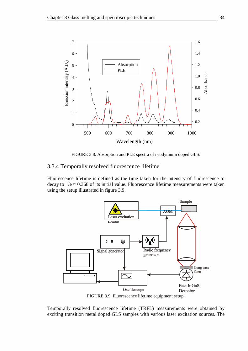
Chapter 3 Glass melting and spectroscopic techniques 34
Wavelength (nm)
500 600 700 800 900 1000
Abs
orb
ance
0.2
0.4
0.6
0.8
1.0
1.2
1.4
1.6
Em
issi
on
inte
nsity
(A
.U.)
0
1
2
3
4
5
6
7
AbsorptionPLE
FIGURE 3.8. Absorption and PLE spectra of neodymium doped GLS. 3.3.4 Temporally resolved fluorescence lifetime Fluorescence lifetime is defined as the time taken for the intensity of fluorescence to decay to 1/e ≈ 0.368 of its initial value. Fluorescence lifetime measurements were taken using the setup illustrated in figure 3.9.
FIGURE 3.9. Fluorescence lifetime equipment setup.
Temporally resolved fluorescence lifetime (TRFL) measurements were obtained by exciting transition metal doped GLS samples with various laser excitation sources. The
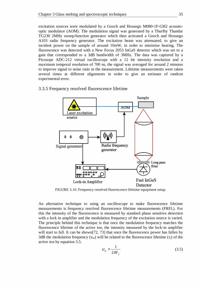
Chapter 3 Glass melting and spectroscopic techniques 35
excitation sources were modulated by a Gooch and Housego M080-1F-GH2 acousto-optic modulator (AOM). The modulation signal was generated by a Thurlby Thandar TG230 2MHz sweep/function generator which then activated a Gooch and Housego A103 radio frequency generator. The excitation beam was attenuated, to give an incident power on the sample of around 10mW, in order to minimise heating. The fluorescence was detected with a New Focus 2053 InGaS detector which was set to a gain that corresponded to a 3dB bandwidth of 3MHz. The data was captured by a Picosope ADC-212 virtual oscilloscope with a 12 bit intensity resolution and a maximum temporal resolution of 700 ns, the signal was averaged for around 2 minutes to improve signal to noise ratio in the measurement. Lifetime measurements were taken several times at different alignments in order to give an estimate of random experimental error. 3.3.5 Frequency resolved fluorescence lifetime
FIGURE 3.10. Frequency resolved fluorescence lifetime equipment setup.
An alternative technique to using an oscilloscope to make fluorescence lifetime measurements is frequency resolved fluorescence lifetime measurements (FRFL). For this the intensity of the fluorescence is measured by standard phase sensitive detection with a lock in amplifier and the modulation frequency of the excitation source is varied. The principle behind this technique is that once the modulation frequency matches the fluorescence lifetime of the active ion, the intensity measured by the lock-in amplifier will start to fall. It can be shown[72, 73] that once the fluorescence power has fallen by 3dB the modulation frequency (υm) will be related to the fluorescence lifetime (τf) of the active ion by equation 3.5.
fm πτ
υ2
1= (3.5)
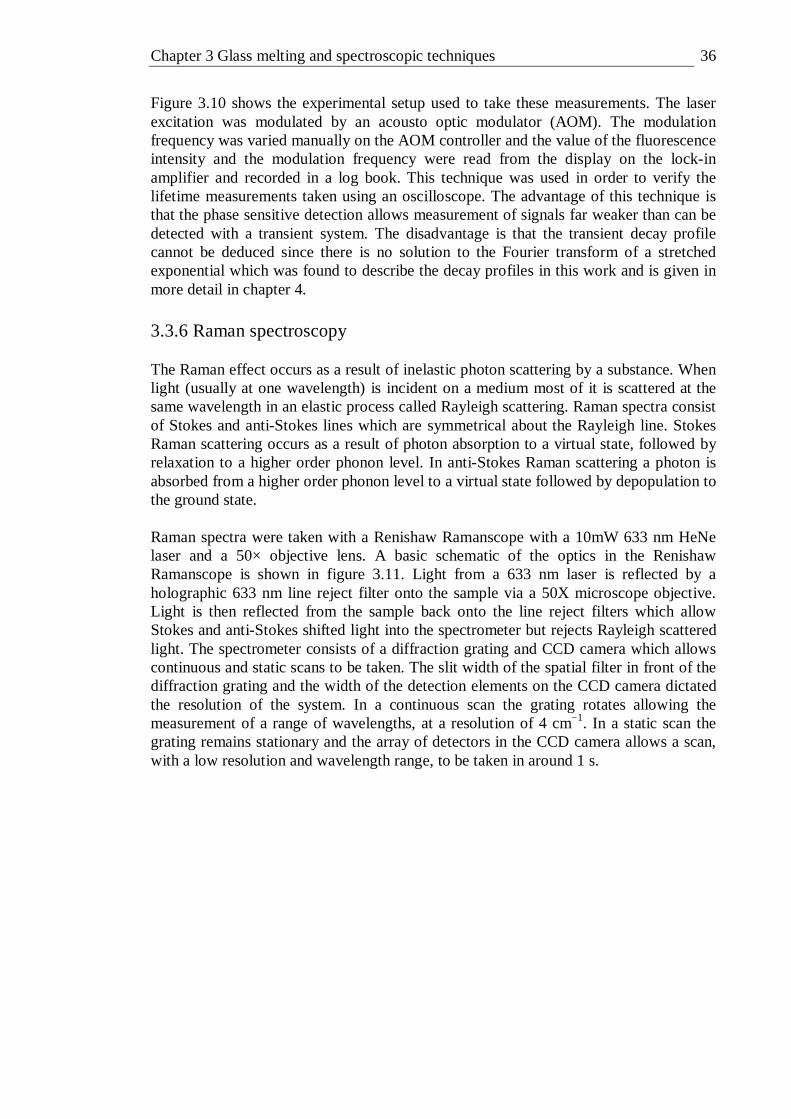
Chapter 3 Glass melting and spectroscopic techniques 36
Figure 3.10 shows the experimental setup used to take these measurements. The laser excitation was modulated by an acousto optic modulator (AOM). The modulation frequency was varied manually on the AOM controller and the value of the fluorescence intensity and the modulation frequency were read from the display on the lock-in amplifier and recorded in a log book. This technique was used in order to verify the lifetime measurements taken using an oscilloscope. The advantage of this technique is that the phase sensitive detection allows measurement of signals far weaker than can be detected with a transient system. The disadvantage is that the transient decay profile cannot be deduced since there is no solution to the Fourier transform of a stretched exponential which was found to describe the decay profiles in this work and is given in more detail in chapter 4. 3.3.6 Raman spectroscopy The Raman effect occurs as a result of inelastic photon scattering by a substance. When light (usually at one wavelength) is incident on a medium most of it is scattered at the same wavelength in an elastic process called Rayleigh scattering. Raman spectra consist of Stokes and anti-Stokes lines which are symmetrical about the Rayleigh line. Stokes Raman scattering occurs as a result of photon absorption to a virtual state, followed by relaxation to a higher order phonon level. In anti-Stokes Raman scattering a photon is absorbed from a higher order phonon level to a virtual state followed by depopulation to the ground state. Raman spectra were taken with a Renishaw Ramanscope with a 10mW 633 nm HeNe laser and a 50× objective lens. A basic schematic of the optics in the Renishaw Ramanscope is shown in figure 3.11. Light from a 633 nm laser is reflected by a holographic 633 nm line reject filter onto the sample via a 50X microscope objective. Light is then reflected from the sample back onto the line reject filters which allow Stokes and anti-Stokes shifted light into the spectrometer but rejects Rayleigh scattered light. The spectrometer consists of a diffraction grating and CCD camera which allows continuous and static scans to be taken. The slit width of the spatial filter in front of the diffraction grating and the width of the detection elements on the CCD camera dictated the resolution of the system. In a continuous scan the grating rotates allowing the measurement of a range of wavelengths, at a resolution of 4 cm−1. In a static scan the grating remains stationary and the array of detectors in the CCD camera allows a scan, with a low resolution and wavelength range, to be taken in around 1 s.

Chapter 3 Glass melting and spectroscopic techniques 37
FIGURE 3.11 Schematic representation of micro Raman system.
3.3.7 Quantum efficiency The quantum efficiency (QE) was measured by taking spectra of both the fluorescence and the excitation laser using standard phase sensitive detection, with a lock-in amplifier and monochromator. The important difference compared to standard fluorescence measurements, was that the sample was placed inside an integrating sphere. An integrating sphere is a hollow sphere coated on the inside with a material that reflects diffusely and has a high reflectivity. The effect of this is that any light entering, or produced within, the sphere becomes distributed isotropically, therefore the flux received at an aperture in the sphere is proportional to the total amount of light entering or produced within the sphere. The integrating sphere used was a Labsphere model FM-040-SF which has an interior coating of a highly reflective white paint (“Spectraflect”) and was around 15cm in diameter. A custom built sample holder was produced consisting of a small crocodile clip attached to the end of a brass thread, this went through a threaded and polished aluminium plate which was clamped to one of the ports of the integrating sphere. This sample holder allowed fine adjustment of the samples’ position in the integrating sphere by turning the brass thread. Because of the sample holders’ small surface area and relatively high reflectivity, it was not thought to significantly degrade the performance of the integrating sphere. The baffle was also moved from its original position on the inside surface of the sphere to one where it covered the exit aperture, so that there was no direct line of sight from the sample to the detector. The original baffle position was found to give anomalous results, thought to result from laser light being scattered from the sample directly into the exit aperture. The setup used is illustrated in Figure 3.12.
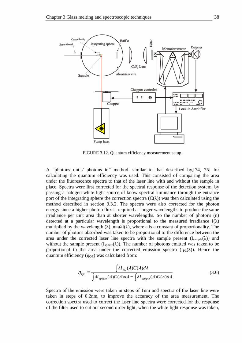
Chapter 3 Glass melting and spectroscopic techniques 38
FIGURE 3.12. Quantum efficiency measurement setup. A “photons out / photons in” method, similar to that described by,[74, 75] for calculating the quantum efficiency was used. This consisted of comparing the area under the fluorescence spectra to that of the laser line with and without the sample in place. Spectra were first corrected for the spectral response of the detection system, by passing a halogen white light source of know spectral luminance through the entrance port of the integrating sphere the correction spectra (C(λ)) was then calculated using the method described in section 3.3.2. The spectra were also corrected for the photon energy since a higher photon flux is required at longer wavelengths to produce the same irradiance per unit area than at shorter wavelengths. So the number of photons (n) detected at a particular wavelength is proportional to the measured irradiance I(λ) multiplied by the wavelength (λ), n=aλI(λ), where a is a constant of proportionality. The number of photons absorbed was taken to be proportional to the difference between the area under the corrected laser line spectra with the sample present (Isample(λ)) and without the sample present (Isphere(λ)). The number of photons emitted was taken to be proportional to the area under the corrected emission spectra (IPL(λ)). Hence the quantum efficiency (ηQE) was calculated from:
∫∫∫
−=
λλλλλλλλ
λλλλη
dCIdCI
dCI
samplesphere
PL
QE)()()()(
)()( (3.6)
Spectra of the emission were taken in steps of 1nm and spectra of the laser line were taken in steps of 0.2nm, to improve the accuracy of the area measurement. The correction spectra used to correct the laser line spectra were corrected for the response of the filter used to cut out second order light, when the white light response was taken,
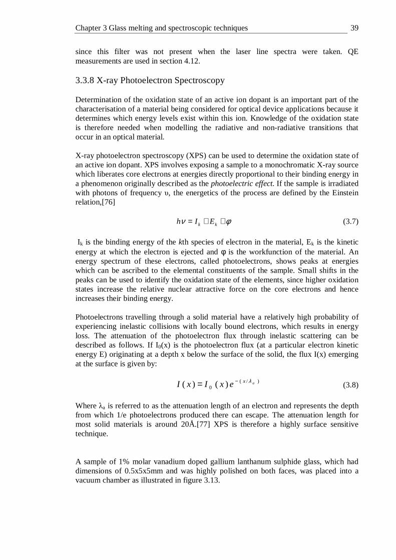
Chapter 3 Glass melting and spectroscopic techniques 39
since this filter was not present when the laser line spectra were taken. QE measurements are used in section 4.12. 3.3.8 X-ray Photoelectron Spectroscopy Determination of the oxidation state of an active ion dopant is an important part of the characterisation of a material being considered for optical device applications because it determines which energy levels exist within this ion. Knowledge of the oxidation state is therefore needed when modelling the radiative and non-radiative transitions that occur in an optical material. X-ray photoelectron spectroscopy (XPS) can be used to determine the oxidation state of an active ion dopant. XPS involves exposing a sample to a monochromatic X-ray source which liberates core electrons at energies directly proportional to their binding energy in a phenomenon originally described as the photoelectric effect. If the sample is irradiated with photons of frequency υ, the energetics of the process are defined by the Einstein relation,[76]
φν ++= kk EIh (3.7)
Ik is the binding energy of the kth species of electron in the material, Ek is the kinetic energy at which the electron is ejected and φ is the workfunction of the material. An energy spectrum of these electrons, called photoelectrons, shows peaks at energies which can be ascribed to the elemental constituents of the sample. Small shifts in the peaks can be used to identify the oxidation state of the elements, since higher oxidation states increase the relative nuclear attractive force on the core electrons and hence increases their binding energy. Photoelectrons travelling through a solid material have a relatively high probability of experiencing inelastic collisions with locally bound electrons, which results in energy loss. The attenuation of the photoelectron flux through inelastic scattering can be described as follows. If I0(x) is the photoelectron flux (at a particular electron kinetic energy E) originating at a depth x below the surface of the solid, the flux I(x) emerging at the surface is given by:
)/(0 )()( axexIxI λ−= (3.8)
Where λa is referred to as the attenuation length of an electron and represents the depth from which 1/e photoelectrons produced there can escape. The attenuation length for most solid materials is around 20Å.[77] XPS is therefore a highly surface sensitive technique. A sample of 1% molar vanadium doped gallium lanthanum sulphide glass, which had dimensions of 0.5x5x5mm and was highly polished on both faces, was placed into a vacuum chamber as illustrated in figure 3.13.
Chapter 3 Glass melting and spectroscopic techniques 40
FIGURE 3.13. X-ray photoelectron spectra equipment schematic.
The vacuum chamber was evacuated to around 10-9 mbar and the sample was exposed to X-ray radiation from an Mg Kα anode source centred at 1253.6 eV. The FWHM of the anode source limited the resolution of the photoelectron spectra to 1eV. Higher resolution can be obtained using a monochromated X-ray source, however this comes at the expense of counts, due to the larger source-sample separation. An initial photoelectron spectrum was taken and no vanadium signature was detected but around 75% carbon was detected. This was believed to be a surface effect caused by polishing. The sample was then sputtered for 30 minutes with a 5 keV Ar ion sputterer in order to remove any surface contamination, photoelectron spectra indicated no vanadium to be present and a high carbon signature. Further photoelectron spectra taken after 1 and 2 hours of sputtering indicated that no vanadium was present and a high carbon signature. It is believed that the effects of polishing penetrated the sample further than can be practically removed by sputtering. So a sample was then fractured by tapping sharply with a razor blade. It was noted that fractures were conchoidal, typical of fractures in brittle materials that have no natural planes of separation. After several attempts a roughly flat face of around 5x5mm was obtained, this was placed immediately into the vacuum chamber and evacuated in order to minimise any atmospheric reaction. The sample introduction chamber was pumped for ~12 hours to allow for the sample out-gassing. A weak vanadium signature was found, in order to obtain good signal to noise, a spectrum was collected over an 8 hour period. XPS measurements are used in section 4.13. XPS measurements and analysis where carried out under the supervision of Dr. N. Blanchard using facilities of the Advanced Technology Institute, University of Surrey.
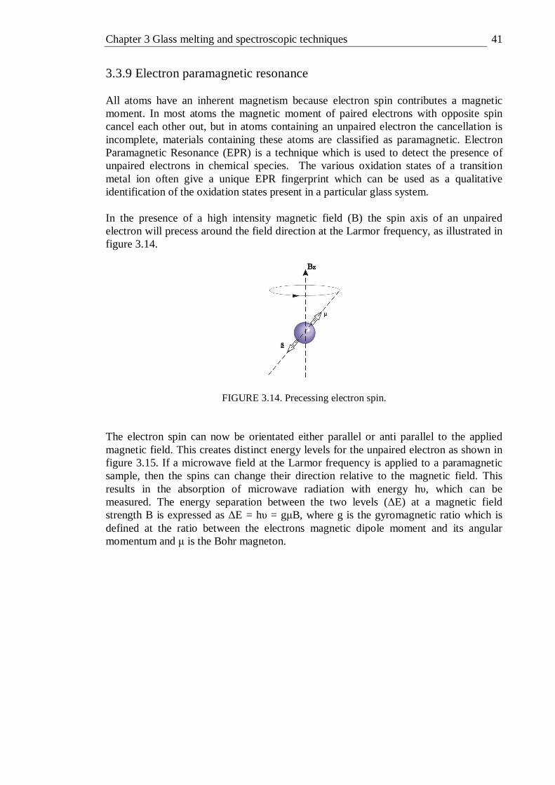
Chapter 3 Glass melting and spectroscopic techniques 41
3.3.9 Electron paramagnetic resonance All atoms have an inherent magnetism because electron spin contributes a magnetic moment. In most atoms the magnetic moment of paired electrons with opposite spin cancel each other out, but in atoms containing an unpaired electron the cancellation is incomplete, materials containing these atoms are classified as paramagnetic. Electron Paramagnetic Resonance (EPR) is a technique which is used to detect the presence of unpaired electrons in chemical species. The various oxidation states of a transition metal ion often give a unique EPR fingerprint which can be used as a qualitative identification of the oxidation states present in a particular glass system. In the presence of a high intensity magnetic field (B) the spin axis of an unpaired electron will precess around the field direction at the Larmor frequency, as illustrated in figure 3.14.
FIGURE 3.14. Precessing electron spin. The electron spin can now be orientated either parallel or anti parallel to the applied magnetic field. This creates distinct energy levels for the unpaired electron as shown in figure 3.15. If a microwave field at the Larmor frequency is applied to a paramagnetic sample, then the spins can change their direction relative to the magnetic field. This results in the absorption of microwave radiation with energy hυ, which can be measured. The energy separation between the two levels (∆E) at a magnetic field strength B is expressed as ∆E = hυ = gµB, where g is the gyromagnetic ratio which is defined at the ratio between the electrons magnetic dipole moment and its angular momentum and µ is the Bohr magneton.
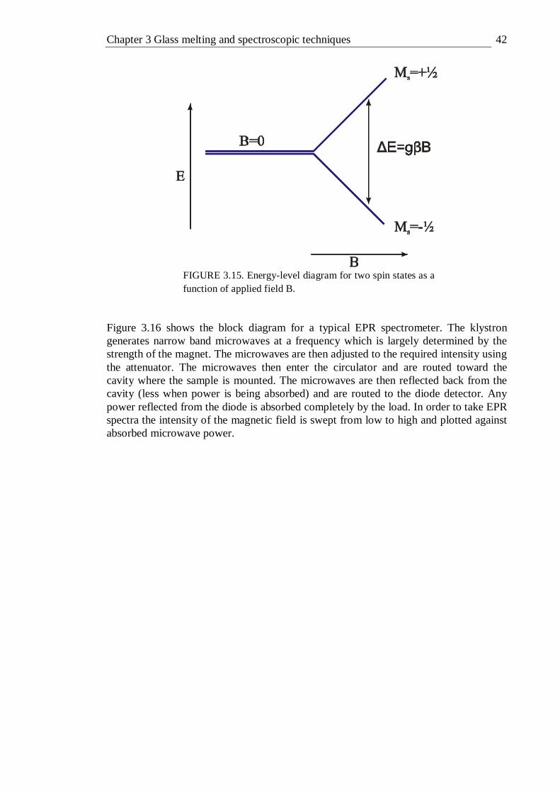
Chapter 3 Glass melting and spectroscopic techniques 42
FIGURE 3.15. Energy-level diagram for two spin states as a function of applied field B.
Figure 3.16 shows the block diagram for a typical EPR spectrometer. The klystron generates narrow band microwaves at a frequency which is largely determined by the strength of the magnet. The microwaves are then adjusted to the required intensity using the attenuator. The microwaves then enter the circulator and are routed toward the cavity where the sample is mounted. The microwaves are then reflected back from the cavity (less when power is being absorbed) and are routed to the diode detector. Any power reflected from the diode is absorbed completely by the load. In order to take EPR spectra the intensity of the magnetic field is swept from low to high and plotted against absorbed microwave power.

Chapter 3 Glass melting and spectroscopic techniques 43
FIGURE 3.16. Schematic block diagram for a typical EPR experimental setup.
In practice this technique alone gives a very poor signal to noise ratio. However the signal to noise ratio can be greatly improved by introducing a small amplitude magnetic field modulation superimposed on the large d.c. magnetic field by small magnetic coils. This allows the use of phase sensitive detection which selects the a.c. component of the diode current. The detected a.c. signal is proportional to the change in sample absorption which amounts to detection of the first derivative of the absorption curve. EPR measurements of vanadium doped GLS were taken on two different systems the first operated with H-fields of around 0.3 Tesla, corresponding to microwave frequencies of about 10GHz (X band). The second was a “high field EPR” instrument operating with H-fields of up to 8 Tesla, corresponding to microwave frequencies of 80-300 GHz. The high field instrument had a sensitivity and resolution which is between 100 and 100,000 times better than the X-band system.[78] The samples required no special preparation but needed to have dimensions of 1-5mm diameter, hence all samples measured were irregular shaped pieces with a diameter of around 3mm. EPR measurements are used in section 4.14. EPR measurements where carried out using facilities of the School of Physics and Astronomy, University of St-Andrews, by Dr. Hassane El Mkami.
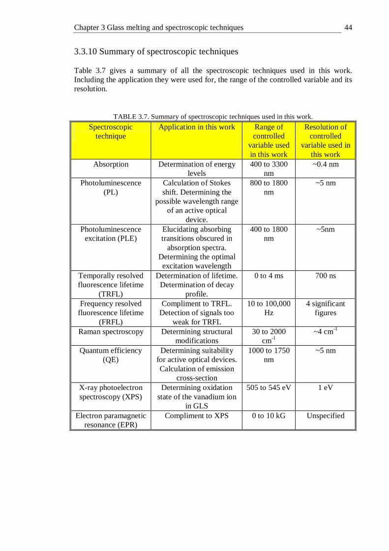
Chapter 3 Glass melting and spectroscopic techniques 44
3.3.10 Summary of spectroscopic techniques Table 3.7 gives a summary of all the spectroscopic techniques used in this work. Including the application they were used for, the range of the controlled variable and its resolution.
TABLE 3.7. Summary of spectroscopic techniques used in this work.
Spectroscopic technique
Application in this work Range of controlled
variable used in this work
Resolution of controlled
variable used in this work
Absorption Determination of energy levels
400 to 3300 nm
~0.4 nm
Photoluminescence (PL)
Calculation of Stokes shift. Determining the
possible wavelength range of an active optical
device.
800 to 1800 nm
~5 nm
Photoluminescence excitation (PLE)
Elucidating absorbing transitions obscured in
absorption spectra. Determining the optimal excitation wavelength
400 to 1800 nm
~5nm
Temporally resolved fluorescence lifetime
(TRFL)
Determination of lifetime. Determination of decay
profile.
0 to 4 ms 700 ns
Frequency resolved fluorescence lifetime
(FRFL)
Compliment to TRFL. Detection of signals too
weak for TRFL
10 to 100,000 Hz
4 significant figures
Raman spectroscopy Determining structural modifications
30 to 2000 cm-1
~4 cm-1
Quantum efficiency (QE)
Determining suitability for active optical devices. Calculation of emission
cross-section
1000 to 1750 nm
~5 nm
X-ray photoelectron spectroscopy (XPS)
Determining oxidation state of the vanadium ion
in GLS
505 to 545 eV 1 eV
Electron paramagnetic resonance (EPR)
Compliment to XPS 0 to 10 kG Unspecified

Chapter 4 Vanadium doped chalcogenide glass 45
Chapter 4
Vanadium doped chalcogenide glass 4.1 Introduction Transition metals have long been used as the active ion in solid state lasers. In fact, laser action was first demonstrated in 1960 in a system which used Cr3+ doped Al2O3 (ruby) as the active medium.[79] Since then a number of transition metal ions have been used in tuneable laser sources, the most successful of which has been the Ti3+ doped Al2O3 (Ti:Sapphire) laser which is tuneable from 690-1100 nm[19] and has been used to generate ultra short laser pulses with durations of 8 fs.[80] Transition metal ions in glasses are usually regarded as a nuisance because they can exhibit a strong and broad absorption, even at sub ppm concentrations, which can seriously degrade the performance of low loss fibre and active optical devices. Transition metal doped glasses are not often considered for active optical devices because they usually have low quantum efficiencies and short lifetimes which results in a high pump threshold. Because of this most publications reporting the spectroscopy of transition metal doped glasses concentrate on absorption in order to study optical loss mechanisms in the glass, such as in silica fibres[81] and fluoride fibre.[82, 83] The only demonstration of lasing in a non rare-earth metal doped glass know to the author is in a bismuth doped aluminosilicate fibre laser.[84] Transition metal doped GLS including vanadium, chromium, nickel, iron, copper and cobalt has previously been studied by Petrovich who investigated the effect of transition metal ion impurities on the infra red absorption of GLS.[24] The absorption of titanium, vanadium, chromium, nickel, iron, copper and cobalt doped GLS has been reported by Brady.[70] Chromium doped chalcogenide glasses has been studied by Haythornthwaite who investigated these glasses as potential materials for broadband amplification.[85] Optical characterisation of transition metal doped chalcogenides, including V:GLS, was carried out by Aronson.[23] Aronson suggested that vanadium was in a 3+ oxidation state and tetrahedrally coordinated based on comparisons of the optical properties of V:GLS to that of vanadium in other hosts. With the benefit of further measurement and analysis, Aronson’s assignment is revised to octahedral V2+ in this work. There have been relatively few publications reporting the spectroscopy of other vanadium doped glasses. Some of these include the absorption of vanadium in zirconium fluoride glass,[82] silica glass[81] and sodium silicate glass.[86] Even rarer are reports of emission from vanadium doped glass, one of the few examples being vanadium doped phosphate glass.[87] Most of the comparisons made in this chapter are to vanadium doped crystals. Laser action at low temperatures has been reported in V2+ doped CsCaF3[6] and V2+ doped MgF2.[7] Unlike rare earth ions the optically active orbitals of transition metals are not shielded from the surrounding glass ligands. Because of this the optical properties of transition metal ions in glass is strongly affected by the local bonding environment experienced by the ion, including the ligands nature, distance from the ion, coordination and symmetry. This fundamental difference with rare earths makes transition metals less suitable for active optical devices in certain respects. However this means that the optical
Chapter 4 Vanadium doped chalcogenide glass 46
characterisation on transition metals can be used to deduce more information about the local bonding environment in the glass; which, negating optical device applications, justifies characterisation of transition metal doped glass. This chapter presents a rigorous optical characterisation of vanadium doped GLS glass (V:GLS) in the form of absorption, photoluminescence (PL), photoluminescence excitation (PLE), emission lifetime, quantum efficiency, X-ray photoelectron spectroscopy (XPS) and electron paramagnetic resonance (EPR) measurements. As described later in the chapter vanadium exists as a broad range of oxidation states in GLS with V2+ being the only optically active oxidation state. The proportion of the vanadium content that exists as V2+ is unknown. Because of this two concentrations are reported for each sample. In the first three figures (4.1-4.3) the batched vanadium content is quoted which is calculated from the weight of elemental vanadium dopant incorporated with the melt components. All other concentrations quoted are a relative vanadium content which is calculated from the intensity of the vanadium absorption normalised to the highest doping concentration used. The suffixes to the vanadium dopant used in this chapter refer to the oxidation state of the vanadium dopant, not the oxidation state in which it exists in the glass system. These are V(V) for V2O5 and V(III) for V 2S3. Where analyses in terms of Gaussians are used spectral units are give in energy. 4.2 Absorption measurements Absorption spectroscopy is arguably the most fundamental optical characterisation technique. Here it is used to identify the wavelength that transitions between the ground state and excited states of the vanadium ion occur. Absorption measurements were taken with a Varian Cary 500 spectrophotometer, which is described in section 3.3.1. The reference aperture was left blank. The range of the measurements was 400 to 3300 nm. Figure 4.1 shows the absorption spectra of GLS doped with varying concentrations of vanadium. All have a peak at 1100 nm with relative intensities consistent with the doping concentration. The red shift of the band-edge with increasing dopant concentration indicates that there is a strong absorption by vanadium within the GLS band-edge region around 500nm. There is also a shoulder visible around 700 nm indicating a third vanadium absorption band in this region. In addition there is also evidence of a very weak shoulder at around 1000nm which could be attributed to a spin forbidden transition.
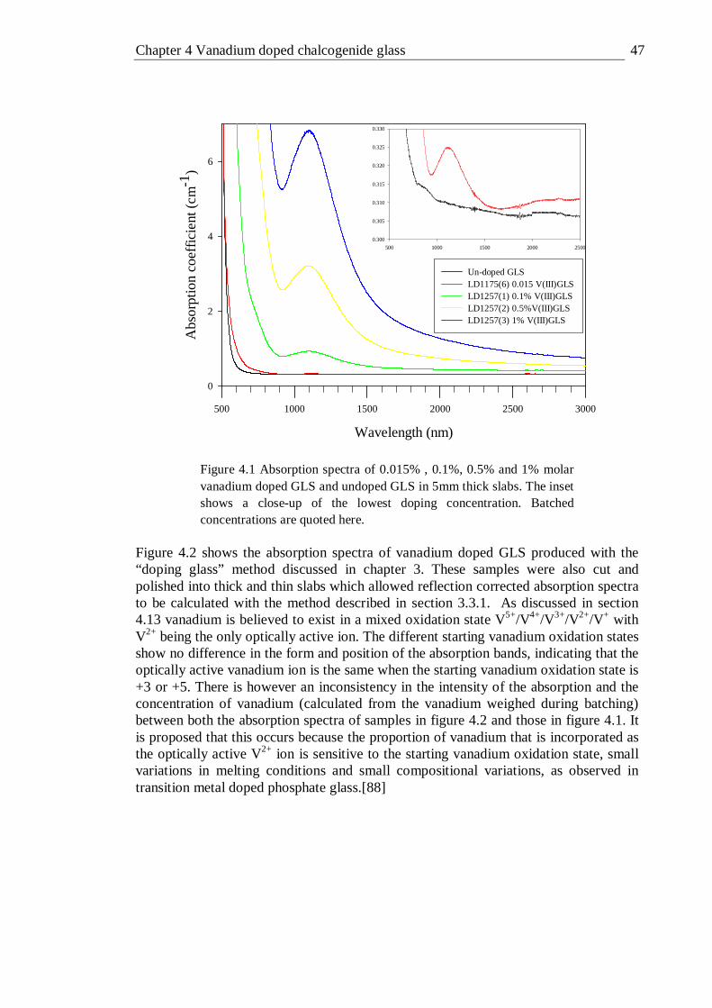
Chapter 4 Vanadium doped chalcogenide glass 47
Wavelength (nm)
500 1000 1500 2000 2500 3000
Abs
orpt
ion
coef
ficie
nt (
cm-1
)
0
2
4
6
Un-doped GLSLD1175(6) 0.015 V(III)GLSLD1257(1) 0.1% V(III)GLS LD1257(2) 0.5%V(III)GLS LD1257(3) 1% V(III)GLS
500 1000 1500 2000 2500
0.300
0.305
0.310
0.315
0.320
0.325
0.330
Figure 4.1 Absorption spectra of 0.015% , 0.1%, 0.5% and 1% molar vanadium doped GLS and undoped GLS in 5mm thick slabs. The inset shows a close-up of the lowest doping concentration. Batched concentrations are quoted here.
Figure 4.2 shows the absorption spectra of vanadium doped GLS produced with the “doping glass” method discussed in chapter 3. These samples were also cut and polished into thick and thin slabs which allowed reflection corrected absorption spectra to be calculated with the method described in section 3.3.1. As discussed in section 4.13 vanadium is believed to exist in a mixed oxidation state V5+/V4+/V3+/V2+/V+ with V2+ being the only optically active ion. The different starting vanadium oxidation states show no difference in the form and position of the absorption bands, indicating that the optically active vanadium ion is the same when the starting vanadium oxidation state is +3 or +5. There is however an inconsistency in the intensity of the absorption and the concentration of vanadium (calculated from the vanadium weighed during batching) between both the absorption spectra of samples in figure 4.2 and those in figure 4.1. It is proposed that this occurs because the proportion of vanadium that is incorporated as the optically active V2+ ion is sensitive to the starting vanadium oxidation state, small variations in melting conditions and small compositional variations, as observed in transition metal doped phosphate glass.[88]
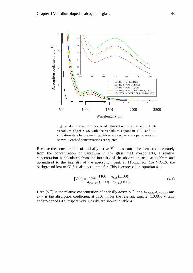
Chapter 4 Vanadium doped chalcogenide glass 48
Wavelength (nm)
500 1000 1500 2000 2500
Ab
sorp
tion
coef
ficie
nt (
cm-1
)
0
1
2
3
4
LD1285(1) Un-doped GLS LD1285(2) 0.1% V(III) GLSLD1285(3) 0.1% V(V) GLS LD1285(4) 0.1% V(III) + 0.05%Ag GLSLD1285(5) 0.1%V(III) GLS + 0.05% Cu(III)
800 900 1000 1100 1200 1300 1400
0.2
0.3
0.4
0.5
0.6
0.7
Figure 4.2 Reflection corrected absorption spectra of 0.1 % vanadium doped GLS with the vanadium dopant in a +3 and +5 oxidation state before melting. Silver and copper co-dopants are also shown. Batched concentrations are quoted.
Because the concentration of optically active V2+ ions cannot be measured accurately from the concentration of vanadium in the glass melt components, a relative concentration is calculated from the intensity of the absorption peak at 1100nm and normalised to the intensity of the absorption peak at 1100nm for 1% V:GLS, the background loss of GLS is also accounted for. This is expressed in equation 4.1.
)1100()1100(
)1100()1100(][
:%1
:2
GLSGLSV
GLSGLSV
aa
aaV
−−
=+ (4.1)
Here [V2+] is the relative concentration of optically active V2+ ions, aV:GLS, a1%V:GLS and aGLS is the absorption coefficient at 1100nm for the relevant sample, 1.038% V:GLS and un-doped GLS respectively. Results are shown in table 4.1
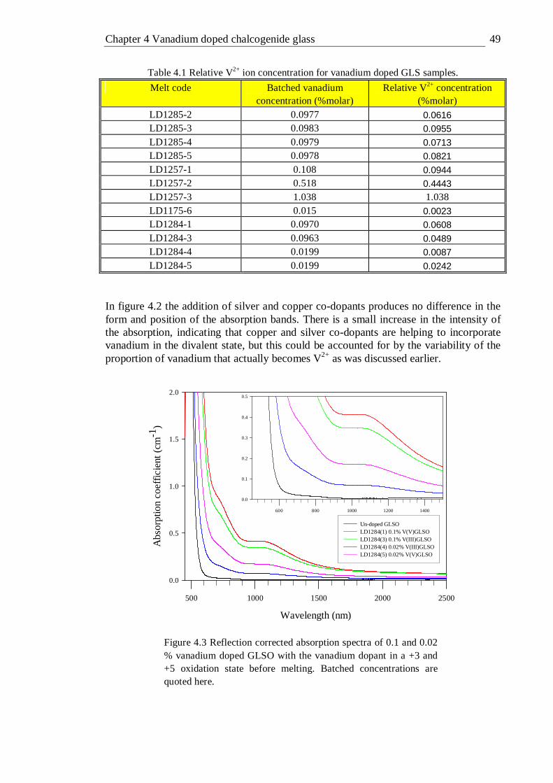
Chapter 4 Vanadium doped chalcogenide glass 49
Table 4.1 Relative V2+ ion concentration for vanadium doped GLS samples.
Melt code Batched vanadium concentration (%molar)
Relative V2+ concentration (%molar)
LD1285-2 0.0977 0.0616 LD1285-3 0.0983 0.0955 LD1285-4 0.0979 0.0713 LD1285-5 0.0978 0.0821 LD1257-1 0.108 0.0944 LD1257-2 0.518 0.4443 LD1257-3 1.038 1.038 LD1175-6 0.015 0.0023 LD1284-1 0.0970 0.0608 LD1284-3 0.0963 0.0489 LD1284-4 0.0199 0.0087 LD1284-5 0.0199 0.0242
In figure 4.2 the addition of silver and copper co-dopants produces no difference in the form and position of the absorption bands. There is a small increase in the intensity of the absorption, indicating that copper and silver co-dopants are helping to incorporate vanadium in the divalent state, but this could be accounted for by the variability of the proportion of vanadium that actually becomes V2+ as was discussed earlier.
Wavelength (nm)
500 1000 1500 2000 2500
Abs
orpt
ion
coe
ffici
ent
(cm-1
)
0.0
0.5
1.0
1.5
2.0
600 800 1000 1200 1400
0.0
0.1
0.2
0.3
0.4
0.5
Un-doped GLSO LD1284(1) 0.1% V(V)GLSOLD1284(3) 0.1% V(III)GLSOLD1284(4) 0.02% V(III)GLSOLD1284(5) 0.02% V(V)GLSO
Figure 4.3 Reflection corrected absorption spectra of 0.1 and 0.02 % vanadium doped GLSO with the vanadium dopant in a +3 and +5 oxidation state before melting. Batched concentrations are quoted here.
Chapter 4 Vanadium doped chalcogenide glass 50
Figure 4.3 shows the reflection corrected absorption of vanadium doped GLSO produced with the “doping glass” method. A notable difference compared to the V:GLS absorption in figure 4.2, is the blue shift in the electronic absorption edge for the un-doped sample. There is still a peak at around 1100nm but its position is less defined as it is more of a shoulder on the absorption at around 700nm. Possible explanations for this are a broadening of one or both of the absorption bands at 700 and 1100 nm and/or an increase in the relative intensity of the absorption band at 700 nm to that at 1100nm. As in V:GLS, doping with V(III) or V(V) show no difference in the form and position of the absorption bands. Similarly to V:GLS there is an inconsistency in the intensity of the absorption and the batched concentration of vanadium. It is also noted that the absorption of the optically active V2+ is consistently higher when GLS and GLSO is doped with V2O5 with vanadium in a +5 oxidation state than with V2S3 with vanadium in a +3 oxidation state. This may be because the V2+ is believed to be preferentially incorporated into a high efficiency oxygen related site and the oxygen from V2O5 could aid in the formation of these sites. It can also be seen that the largest change in absorption is in LD1175-6 which was fabricated at a very low doping concentration without the doping glass method and highlights the difficulty of accurate fabrication of low doping concentration glass with the usual method. From this point on, all vanadium concentrations quoted refer to the relative V2+ concentration given in table 4.1. 4.3 Derivative absorption spectroscopy The mathematical differentiation of spectroscopic data is often used as a resolution enhancement technique, to facilitate the detection and location of poorly resolved spectral components including peaks which appear only as shoulders as well as the isolation of small peaks from an interfering large background absorption.[89] All spectral features that are attributed to optical transitions in transition metals are assumed to be composed of a sum of Gaussian peaks. The standard Gaussian curve function for an absorption band peaking at x0 with absorbance A is:
−−
=
202ln4
0
w
xx
eAA 0th order (4.2)
Where A0 is the maximum band height at x0 and w is the full width at half maximum (FWHM) Differentiation gives:
−−−
−=
202ln4
200 .)(2ln8 w
xx
ew
xxA
dx
dA 1st order (4.3)
−−
−
−=
20
2ln4
2
0
4
02
0
2
2
.2ln8
.)(2ln16 w
xx
ew
A
w
Axx
dx
Ad 2nd order (4.4)

Chapter 4 Vanadium doped chalcogenide glass 51
( )
−−
−−
−=
20
2ln4
6
20
30
4
00
3
3
.)()2ln512()(2ln12 w
xx
ew
xxA
w
xxA
dx
Ad 3rd order (4.5)
The points of inflection on a Gaussian (or any) curve are given when the first derivative is at an extremum and when the second derivative equals zero.[90] By setting equation 4.3 equal to zero it can be shown[91] that the ratio of the FWHM to the width of the Gaussian band between the points of inflection (σ) is given by equation 4.6:
177.12ln2 =⋅=σ
FWHM (4.6)
Higher order derivatives discriminate strongly in favour of narrower bands[92] however the signal-to-noise ratio (SNR) is degraded with increasing differentiation order.[89, 93] Relative signal to noise ratios for unsmoothed derivatives are given in table 4.2. Setting x=x0 for equations 4.2-4.5 gives the peak amplitudes in table 4.2, this shows that second derivatives are inversely proportional to the square of the FWHM.
TABLE 4.2 Peak amplitude and relative signal-to-noise ratio for Gaussian peaks and some derivatives.
Order Peak amplitude at x=x0 Relative SNR 0th order (A) A0 1
1st order
dx
dA
0 2.02/w
2nd order
2
2
dx
Ad 2
02ln8
w
A−
3.26/w2
3rd order
3
3
dx
Ad
0 8.1/w3
In order to improve the signal-to-noise ratio, “running average” smoothing filters (RASF) can be applied. The optimum number of passes for a RASF is believed to be n+1 where n is the derivation order.[89] The relative SNR of the smoothed nth derivative is given by:
WrCW
rWC
W
NC
SNR
SNR nnnn
nnn
n
nnnn 5.0
5.05.0
0
)(
)(
)( +++
=== ααα (4.7)
Where (SNR)0 is the SNR of the unsmoothed 0th derivative. Smoothing with a RASF reduces noise by a factor of Nn+05, where N is the number of data points in the smoothing operation, but reduces the signal by a factor of αn, where r is the sampling proportion and Cn is a constant which depends on the derivative order and band shape. SNR will reach a maximum for sampling proportions of 1,[89] however large sampling proportions cause severe peak height attenuation, As a trade-off between SNR and signal attenuation a sampling proportion of 0.05 was used for this work.
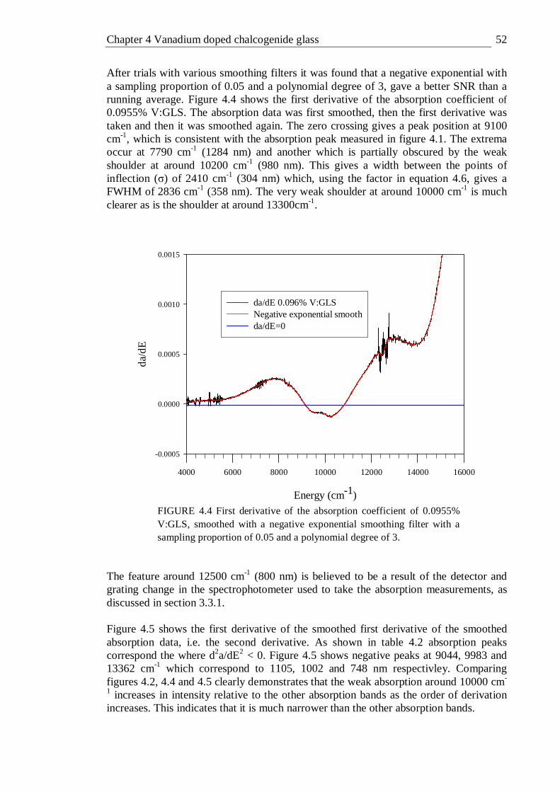
Chapter 4 Vanadium doped chalcogenide glass 52
After trials with various smoothing filters it was found that a negative exponential with a sampling proportion of 0.05 and a polynomial degree of 3, gave a better SNR than a running average. Figure 4.4 shows the first derivative of the absorption coefficient of 0.0955% V:GLS. The absorption data was first smoothed, then the first derivative was taken and then it was smoothed again. The zero crossing gives a peak position at 9100 cm-1, which is consistent with the absorption peak measured in figure 4.1. The extrema occur at 7790 cm-1 (1284 nm) and another which is partially obscured by the weak shoulder at around 10200 cm-1 (980 nm). This gives a width between the points of inflection (σ) of 2410 cm-1 (304 nm) which, using the factor in equation 4.6, gives a FWHM of 2836 cm-1 (358 nm). The very weak shoulder at around 10000 cm-1 is much clearer as is the shoulder at around 13300cm-1.
Energy (cm-1)
4000 6000 8000 10000 12000 14000 16000
da/
dE
-0.0005
0.0000
0.0005
0.0010
0.0015
da/dE 0.096% V:GLSNegative exponential smoothda/dE=0
FIGURE 4.4 First derivative of the absorption coefficient of 0.0955% V:GLS, smoothed with a negative exponential smoothing filter with a sampling proportion of 0.05 and a polynomial degree of 3.
The feature around 12500 cm-1 (800 nm) is believed to be a result of the detector and grating change in the spectrophotometer used to take the absorption measurements, as discussed in section 3.3.1. Figure 4.5 shows the first derivative of the smoothed first derivative of the smoothed absorption data, i.e. the second derivative. As shown in table 4.2 absorption peaks correspond the where d2a/dE2 < 0. Figure 4.5 shows negative peaks at 9044, 9983 and 13362 cm-1 which correspond to 1105, 1002 and 748 nm respectivley. Comparing figures 4.2, 4.4 and 4.5 clearly demonstrates that the weak absorption around 10000 cm-
1 increases in intensity relative to the other absorption bands as the order of derivation increases. This indicates that it is much narrower than the other absorption bands.
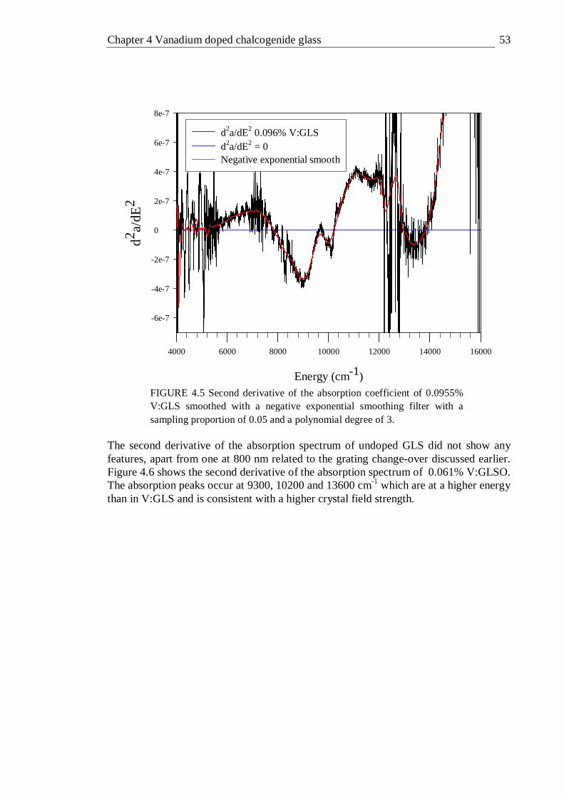
Chapter 4 Vanadium doped chalcogenide glass 53
Energy (cm-1)
4000 6000 8000 10000 12000 14000 16000
d2 a/d
E2
-6e-7
-4e-7
-2e-7
0
2e-7
4e-7
6e-7
8e-7
d2a/dE2 0.096% V:GLSd2a/dE2 = 0Negative exponential smooth
FIGURE 4.5 Second derivative of the absorption coefficient of 0.0955% V:GLS smoothed with a negative exponential smoothing filter with a sampling proportion of 0.05 and a polynomial degree of 3.
The second derivative of the absorption spectrum of undoped GLS did not show any features, apart from one at 800 nm related to the grating change-over discussed earlier. Figure 4.6 shows the second derivative of the absorption spectrum of 0.061% V:GLSO. The absorption peaks occur at 9300, 10200 and 13600 cm-1 which are at a higher energy than in V:GLS and is consistent with a higher crystal field strength.

Chapter 4 Vanadium doped chalcogenide glass 54
Energy (cm-1)
6000 8000 10000 12000 14000 16000
d2 a/d
E2
-1e-5
-5e-6
0
5e-6
1e-5
Negative exponential smoothd2a/dE2 = 0d2a/dE2 0.061% V:GLSO
FIGURE 4.6 Second derivative of the absorption coefficient of 0.061% V:GLSO smoothed with a negative exponential smoothing filter with a sampling proportion of 0.05 and a polynomial degree of 3.
4.4 Photoluminescence of vanadium doped GLS The photoluminescence (PL) of V:GLS reveals the Stokes shift, discussed in section 2.5 and 4.11, and the wavelength range over which an active device based on V:GLS could be used. The measurements were taken using the experimental setup described in section 3.3.2. 4.4.1 Photoluminescence spectra Figures 4.7 to 4.10 show the PL spectra of 0.0023, 0.0944, 0.4443 and 1.038% molar vanadium doped GLS excited at wavelengths of 514, 808 and 1064 nm and temperatures of 77 and 300 K. The excitation wavelengths were chosen as the closest available laser sources that could excite into the three main absorption bands of V:GLS which were identified in section 4.2 and 4.5. The low temperature PL spectra were taken to give an indication of the relative contribution of homogeneous and inhomogeneous broadening. It was not possible to obtain spectra for all combinations of excitation wavelength and temperature in the highly doped samples as emission was significantly weaker than at lower concentrations. This is attributed to re-absorption of the emission and concentration quenching of the excitation.
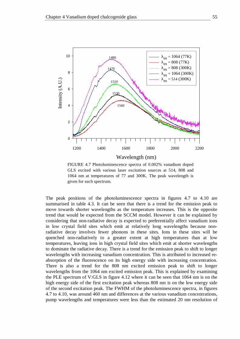
Chapter 4 Vanadium doped chalcogenide glass 55
Wavelength (nm)
1200 1400 1600 1800 2000 2200
Inte
nsity
(A
.U.)
0
2
4
6
8
10 λex = 1064 (77K)λex = 808 (77K)λex = 808 (300K)λex = 1064 (300K)λex = 514 (300K)
1470
1510
1530
1560
1480
FIGURE 4.7 Photoluminescence spectra of 0.002% vanadium doped GLS excited with various laser excitation sources at 514, 808 and 1064 nm at temperatures of 77 and 300K. The peak wavelength is given for each spectrum.
The peak positions of the photoluminescence spectra in figures 4.7 to 4.10 are summarised in table 4.3. It can be seen that there is a trend for the emission peak to move towards shorter wavelengths as the temperature increases. This is the opposite trend that would be expected from the SCCM model. However it can be explained by considering that non-radiative decay is expected to preferentially affect vanadium ions in low crystal field sites which emit at relatively long wavelengths because non-radiative decay involves fewer phonons in these sites. Ions in these sites will be quenched non-radiatively to a greater extent at high temperatures than at low temperatures, leaving ions in high crystal field sites which emit at shorter wavelengths to dominate the radiative decay. There is a trend for the emission peak to shift to longer wavelengths with increasing vanadium concentration. This is attributed to increased re-absorption of the fluorescence on its high energy side with increasing concentration. There is also a trend for the 808 nm excited emission peak to shift to longer wavelengths from the 1064 nm excited emission peak. This is explained by examining the PLE spectrum of V:GLS in figure 4.12 where it can be seen that 1064 nm is on the high energy side of the first excitation peak whereas 808 nm is on the low energy side of the second excitation peak. The FWHM of the photoluminescence spectra, in figures 4.7 to 4.10, was around 460 nm and differences at the various vanadium concentrations, pump wavelengths and temperatures were less than the estimated 20 nm resolution of
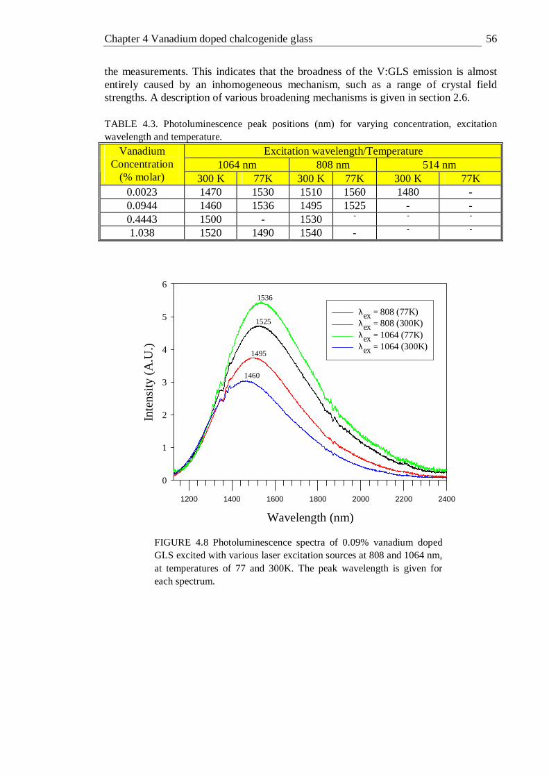
Chapter 4 Vanadium doped chalcogenide glass 56
the measurements. This indicates that the broadness of the V:GLS emission is almost entirely caused by an inhomogeneous mechanism, such as a range of crystal field strengths. A description of various broadening mechanisms is given in section 2.6. TABLE 4.3. Photoluminescence peak positions (nm) for varying concentration, excitation wavelength and temperature.
Excitation wavelength/Temperature 1064 nm 808 nm 514 nm
Vanadium Concentration
(% molar) 300 K 77K 300 K 77K 300 K 77K 0.0023 1470 1530 1510 1560 1480 - 0.0944 1460 1536 1495 1525 - - 0.4443 1500 - 1530 - - -
1.038 1520 1490 1540 - - -
Wavelength (nm)
1200 1400 1600 1800 2000 2200 2400
Inte
nsi
ty (
A.U
.)
0
1
2
3
4
5
6
λex = 808 (77K)λex = 808 (300K)λex = 1064 (77K)λex = 1064 (300K)
1536
1525
1495
1460
FIGURE 4.8 Photoluminescence spectra of 0.09% vanadium doped GLS excited with various laser excitation sources at 808 and 1064 nm, at temperatures of 77 and 300K. The peak wavelength is given for each spectrum.
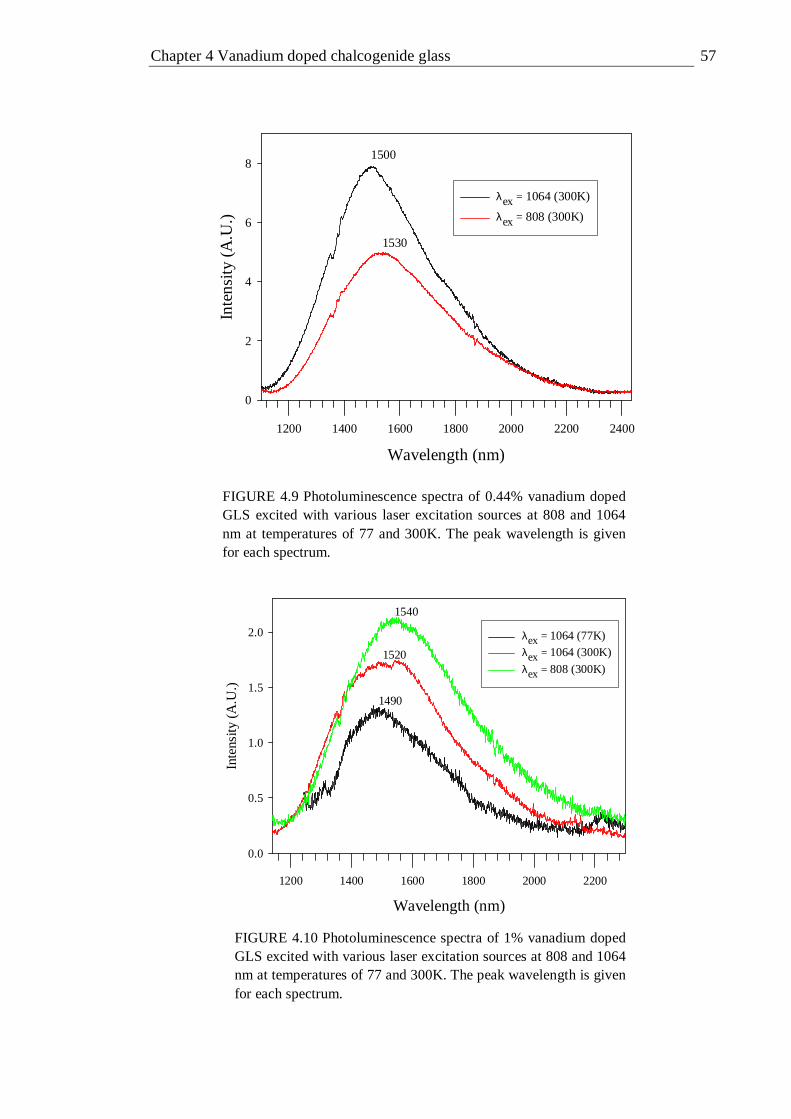
Chapter 4 Vanadium doped chalcogenide glass 57
Wavelength (nm)
1200 1400 1600 1800 2000 2200 2400
Inte
nsi
ty (
A.U
.)
0
2
4
6
8
λex = 1064 (300K)
λex = 808 (300K)
1500
1530
FIGURE 4.9 Photoluminescence spectra of 0.44% vanadium doped GLS excited with various laser excitation sources at 808 and 1064 nm at temperatures of 77 and 300K. The peak wavelength is given for each spectrum.
Wavelength (nm)
1200 1400 1600 1800 2000 2200
Inte
nsity
(A
.U.)
0.0
0.5
1.0
1.5
2.0 λex = 1064 (77K)λex = 1064 (300K)
λex = 808 (300K)
1490
1520
1540
FIGURE 4.10 Photoluminescence spectra of 1% vanadium doped GLS excited with various laser excitation sources at 808 and 1064 nm at temperatures of 77 and 300K. The peak wavelength is given for each spectrum.

Chapter 4 Vanadium doped chalcogenide glass 58
4.4.2 Discussion of photoluminescence spectra Exciting V:GLS at 514, 808 and 1064 nm roughly equates to exciting into each of the three main absorption bands identified for V:GLS in figure 4.12. The PL from excitation at these wavelengths show similar characteristic spectra, peaking at ~1500 nm, with a full width at half maximum FWHM of ~500 nm. This indicates that the three absorption bands belong to the same oxidation state, rather than two or more oxidation states which is commonly observed in transition metal doped glasses[86, 94, 95] and crystals.[96] The broadness of the PL spectra indicates that the vanadium ion is in a low crystal field site. A result of this is that the lowest energy level with a spin allowed transition to the ground state (which is strongly dependent on crystal field strength) is the lowest energy level. Conversely, in a strong crystal field site the lowest spin forbidden level (which is almost independent of crystal field strength) is the lowest energy level. In this case, characteristic narrow R-line emission should be observed, as in V3+ doped phosphate glass[87] and V3+ doped corundum.[97] For comparison the PL of 1064 nm excitation of tetrahedrally coordinated V3+ doped LiGaO2, LiAlO 2 and SrAl2O4 peaks at 1650, 1730 and 1800 nm respectively. The origin of this emission has been assigned to the 3T2(
3F)→3A2(3F) transition.[98] The low
temperature (T=4.2K) photoluminescence spectrum of vanadium doped ZnTe, excited at 529 nm, displays three structured emission bands centred at 3195, 2793 and 2247 nm which have been attributed to internal relaxations of the three charge states V+, V2+ and V3+ respectively; the vanadium ions are tetrahedrally coordinated and have been assigned to the 5E(5D)→5T2(
5D), 4T2(4F)→4T1(
4F) and 3T2(3F)→3A2(
3F) transition respectively.[99] Similarly for vanadium doped ZnS three structured emission bands centred at 2700, 2083 and 1785 nm were observed and attributed to tetrahedral V+, V2+ and V3+ respectively and assigned to the 5E(5D)→5T2(
5D), 4T2(4F)→4T1(
4F) and 3T2(
3F)→3A2(3F) transition respectively.[100] In vanadium doped CdTe the same
respective charge states and transitions occur at 3597, 2898 and 2439 nm.[101] These comparisons and others are detailed in table 4.4 which indicates that the PL peak observed in V:GLS is similar to that observed in V2+ and V3+. Table 4.4 also give the refractive index of ZnS, ZnTe and CdTe which illustrates an interesting trend; the peak emission wavelength of vanadium in 1+,2+ and 3+ oxidation states is directly proportional to the refractive index of the host. This is believed to be related to the degree of covalency of the bonds between the host and vanadium dopant. The nephelauxetic effect, which may be used as a measure of the covalency, is caused by the lowering of the excited state of the ion by the surrounding crystal field.[102]
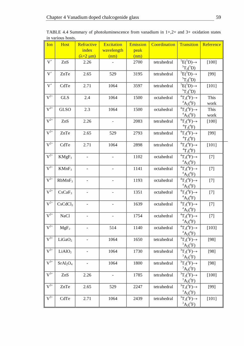
Chapter 4 Vanadium doped chalcogenide glass 59
TABLE 4.4 Summary of photoluminescence from vanadium in 1+,2+ and 3+ oxidation states in various hosts.
Ion Host Refractive index
(λ=2 µm)
Excitation wavelength
(nm)
Emission peak (nm)
Coordination Transition Reference
V+ ZnS 2.26 - 2700 tetrahedral 5E(5D)→ 5T2(
5D) [100]
V+ ZnTe 2.65 529 3195 tetrahedral 5E(5D)→ 5T2(
5D) [99]
V+ CdTe 2.71 1064 3597 tetrahedral 5E(5D)→ 5T2(
5D) [101]
V2+ GLS 2.4 1064 1500 octahedral 4T2(4F)→
4A2(4F)
This work
V2+ GLSO 2.3 1064 1500 octahedral 4T2(4F)→
4A2(4F)
This work
V2+ ZnS 2.26 - 2083 tetrahedral 4T2(4F)→
4T1(4F)
[100]
V2+ ZnTe 2.65 529 2793 tetrahedral 4T2(4F)→
4T1(4F)
[99]
V2+ CdTe 2.71 1064 2898 tetrahedral 4T2(4F)→
4T1(4F)
[101]
V2+ KMgF3 - - 1102 octahedral 4T2(4F)→
4A2(4F)
[7]
V2+ KMnF3 - - 1141 octahedral 4T2(4F)→
4A2(4F)
[7]
V2+ RbMnF3 - - 1193 octahedral 4T2(4F)→
4A2(4F)
[7]
V2+ CsCaF3 - - 1351 octahedral 4T2(4F)→
4A2(4F)
[7]
V2+ CsCdCl3 - - 1639 octahedral 4T2(4F)→
4A2(4F)
[7]
V2+ NaCl - - 1754 octahedral 4T2(4F)→
4A2(4F)
[7]
V2+ MgF2 - 514 1140 octahedral 4T2(4F)→
4A2(4F)
[103]
V3+ LiGaO2 - 1064 1650 tetrahedral 3T2(3F)→
3A2(3F)
[98]
V3+ LiAlO 2 - 1064 1730 tetrahedral 3T2(3F)→
3A2(3F)
[98]
V3+ SrAl2O4 - 1064 1800 tetrahedral 3T2(3F)→
3A2(3F)
[98]
V3+ ZnS 2.26 - 1785 tetrahedral 3T2(3F)→
3A2(3F)
[100]
V3+ ZnTe 2.65 529 2247 tetrahedral 3T2(3F)→
3A2(3F)
[99]
V3+ CdTe 2.71 1064 2439 tetrahedral 3T2(3F)→
3A2(3F)
[101]
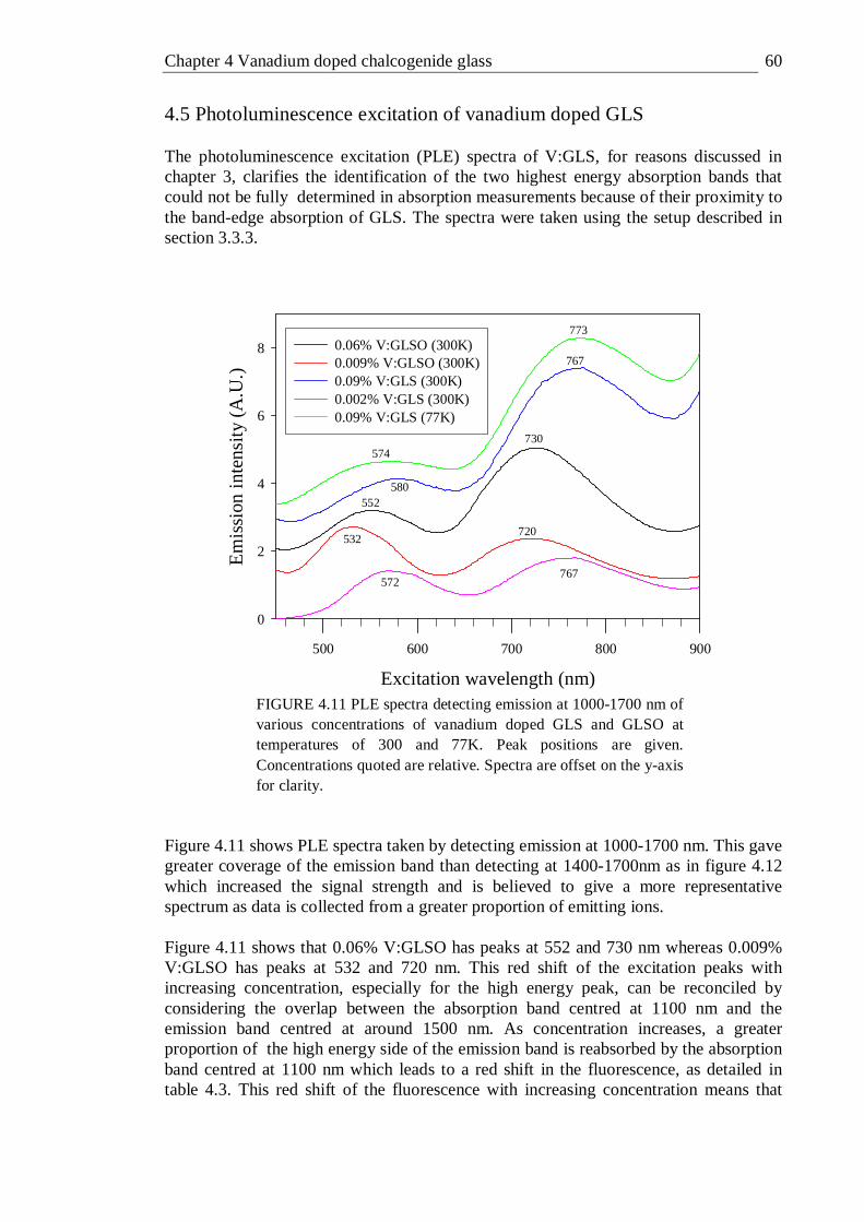
Chapter 4 Vanadium doped chalcogenide glass 60
4.5 Photoluminescence excitation of vanadium doped GLS The photoluminescence excitation (PLE) spectra of V:GLS, for reasons discussed in chapter 3, clarifies the identification of the two highest energy absorption bands that could not be fully determined in absorption measurements because of their proximity to the band-edge absorption of GLS. The spectra were taken using the setup described in section 3.3.3.
Excitation wavelength (nm)
500 600 700 800 900
Em
issi
on in
ten
sity
(A
.U.)
0
2
4
6
8 0.06% V:GLSO (300K)0.009% V:GLSO (300K)0.09% V:GLS (300K)0.002% V:GLS (300K)0.09% V:GLS (77K)
572767
532720
552580
730574
773
767
FIGURE 4.11 PLE spectra detecting emission at 1000-1700 nm of various concentrations of vanadium doped GLS and GLSO at temperatures of 300 and 77K. Peak positions are given. Concentrations quoted are relative. Spectra are offset on the y-axis for clarity.
Figure 4.11 shows PLE spectra taken by detecting emission at 1000-1700 nm. This gave greater coverage of the emission band than detecting at 1400-1700nm as in figure 4.12 which increased the signal strength and is believed to give a more representative spectrum as data is collected from a greater proportion of emitting ions. Figure 4.11 shows that 0.06% V:GLSO has peaks at 552 and 730 nm whereas 0.009% V:GLSO has peaks at 532 and 720 nm. This red shift of the excitation peaks with increasing concentration, especially for the high energy peak, can be reconciled by considering the overlap between the absorption band centred at 1100 nm and the emission band centred at around 1500 nm. As concentration increases, a greater proportion of the high energy side of the emission band is reabsorbed by the absorption band centred at 1100 nm which leads to a red shift in the fluorescence, as detailed in table 4.3. This red shift of the fluorescence with increasing concentration means that
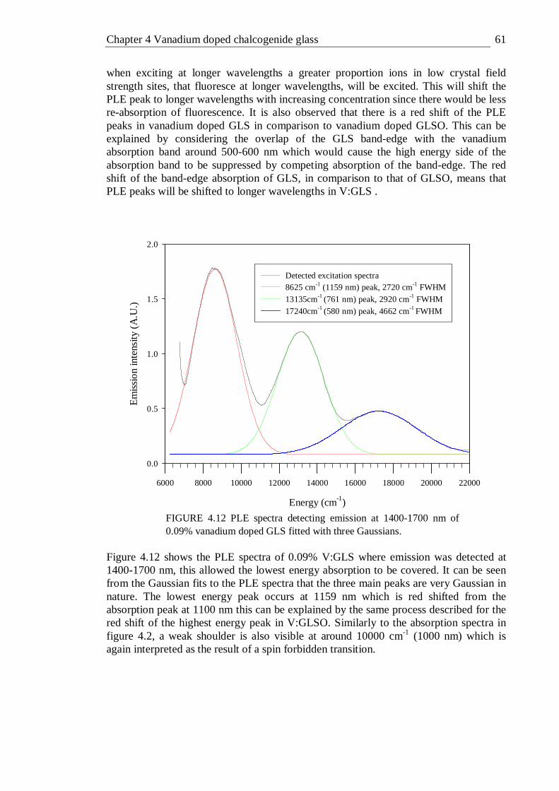
Chapter 4 Vanadium doped chalcogenide glass 61
when exciting at longer wavelengths a greater proportion ions in low crystal field strength sites, that fluoresce at longer wavelengths, will be excited. This will shift the PLE peak to longer wavelengths with increasing concentration since there would be less re-absorption of fluorescence. It is also observed that there is a red shift of the PLE peaks in vanadium doped GLS in comparison to vanadium doped GLSO. This can be explained by considering the overlap of the GLS band-edge with the vanadium absorption band around 500-600 nm which would cause the high energy side of the absorption band to be suppressed by competing absorption of the band-edge. The red shift of the band-edge absorption of GLS, in comparison to that of GLSO, means that PLE peaks will be shifted to longer wavelengths in V:GLS .
Energy (cm-1)
6000 8000 10000 12000 14000 16000 18000 20000 22000
Em
issi
on
inte
nsity
(A
.U.)
0.0
0.5
1.0
1.5
2.0
Detected excitation spectra8625 cm-1 (1159 nm) peak, 2720 cm-1 FWHM13135cm-1 (761 nm) peak, 2920 cm-1 FWHM17240cm-1 (580 nm) peak, 4662 cm-1 FWHM
FIGURE 4.12 PLE spectra detecting emission at 1400-1700 nm of 0.09% vanadium doped GLS fitted with three Gaussians.
Figure 4.12 shows the PLE spectra of 0.09% V:GLS where emission was detected at 1400-1700 nm, this allowed the lowest energy absorption to be covered. It can be seen from the Gaussian fits to the PLE spectra that the three main peaks are very Gaussian in nature. The lowest energy peak occurs at 1159 nm which is red shifted from the absorption peak at 1100 nm this can be explained by the same process described for the red shift of the highest energy peak in V:GLSO. Similarly to the absorption spectra in figure 4.2, a weak shoulder is also visible at around 10000 cm-1 (1000 nm) which is again interpreted as the result of a spin forbidden transition.
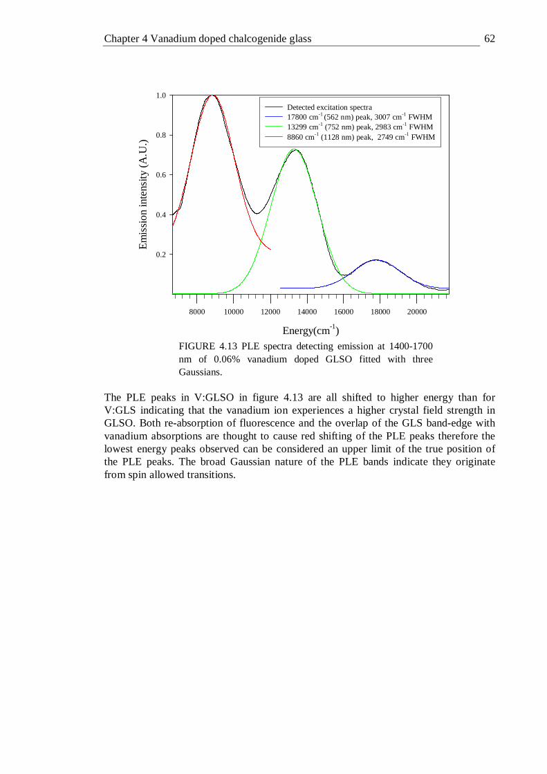
Chapter 4 Vanadium doped chalcogenide glass 62
Energy(cm-1)
8000 10000 12000 14000 16000 18000 20000
Em
issi
on
inte
nsity
(A
.U.)
0.2
0.4
0.6
0.8
1.0
Detected excitation spectra17800 cm-1 (562 nm) peak, 3007 cm-1 FWHM13299 cm-1 (752 nm) peak, 2983 cm-1 FWHM8860 cm-1 (1128 nm) peak, 2749 cm-1 FWHM
FIGURE 4.13 PLE spectra detecting emission at 1400-1700 nm of 0.06% vanadium doped GLSO fitted with three Gaussians.
The PLE peaks in V:GLSO in figure 4.13 are all shifted to higher energy than for V:GLS indicating that the vanadium ion experiences a higher crystal field strength in GLSO. Both re-absorption of fluorescence and the overlap of the GLS band-edge with vanadium absorptions are thought to cause red shifting of the PLE peaks therefore the lowest energy peaks observed can be considered an upper limit of the true position of the PLE peaks. The broad Gaussian nature of the PLE bands indicate they originate from spin allowed transitions.
Chapter 4 Vanadium doped chalcogenide glass 63
4.6 Fluorescence Lifetime Fluorescence lifetime measurements are one of the simplest and most reliable optical characterisation techniques.[104] However, in the case of non-exponential decay (as observed in V:GLS) interpretation can be far from trivial. In this section the fluorescence decay of V:GLS is analysed using stretched exponential, bi exponential, average lifetime, frequency resolved lifetime and continuous lifetime distribution models. From the analysis solid conclusions are drawn as to the local environment of the vanadium ion. 4.6.1 Introduction to the stretched exponential function Many relaxation processes in complex condensed systems such as glasses have long been known to follow the Kohlraush-Williams-Watts (KWW) function,[105] which is also currently know as the stretched exponential function and is given in equation 4.8
−+=β
τt
IytI exp)( 00 (4.8)
Where τ is a characteristic relaxation time, β is the stretch factor (ranging between 0 and 1) and y0 is the offset. The closer β is to 0 the more the function deviates from a single exponential. Stretched exponential relaxation was first described by Kohlraush in 1847 to model the decay of the residual charge on a glass Leyden jar. Since then the stretched exponential function has been shown to fit many other relaxation processes in amorphous materials such as nuclear relaxation,[105] magnetic susceptibility relaxation,[105] fluorescence decay[106] and photoinduced dichroism.[107] Stretched exponential behaviour is rarely observed in crystalline solids; with some exceptions.[108] There have been several mutually exclusive microscopic explanations for the observed stretched exponential relaxation in glasses, this can be seen as being due to the use of different models of the fundamental structure of glasses. The models for stretched exponential relaxation behaviour in glasses generally fall into two categories: spatially heterogeneous dynamics and temporally heterogeneous dynamics. The spatially heterogeneous dynamic model assumes that the relaxation of a single excited ion follows a single exponential law and that the system remains homogeneous over the time taken for the relaxation to occur. Validation of this model has been allowed through the development of fluorescence microscopy which allows the study of single molecules in complex condensed environments.[109] It has been shown that that the fluorescence decay of a single molecule in varying local environments leads to a stretched-exponential decay as a result of the presence of a continuous distribution of lifetimes.[110, 111] The temporally heterogeneous dynamics model assumes that the system remains homogeneous in space but that random sinks, in disordered material such as glass, capture excitations and become progressively depleted with time. This causes the decay rate itself to slow with the progress of time, stretching the decay. These two processes may occur at the same time in a given relaxation process.

Chapter 4 Vanadium doped chalcogenide glass 64
4.6.2 Experimental and analysis techniques Temporally resolved fluorescence lifetime (TRFL) measurements were obtained using the experimental setup described in 3.3.4 and a 1064 nm laser source. An estimate of random experimental error was obtained by taking the measurements several times at different alignments. Regression analysis was implemented using the Marquardt-Levenberg algorithm,[112] given in equation 4.9. This algorithm seeks the values of the parameters that minimize the sum of the squared (SS) differences between the values of the observed and predicted values of the dependent variable.
2
1
)ˆ(∑=
−=n
iii yySS (4.9)
Where yi is the observed and ŷi is the predicted value of the dependent variable, the index i refers to the ith data point and n is the total number of data points. The goodness of the fit was measured using the coefficient of determination (R2), given in equation 4.10.
2
1
2
12
)(
)ˆ(
yy
yyR n
ii
n
ii
∑
∑
=
=
−
−= (4.10)
Wherey is the mean value of the observed dependant variable. The coefficient of determination indicates how much of the total variation in the dependent variable can be accounted for by the regressor function. If R2 = 1 then this indicates that the fitted model explains all variability in the observed dependant variable, while R2 = 0 indicates no linear relationship between the dependant variable and regressors. The fitting procedure was found to return exactly the same results if the fitting of the decay was carried out up to a time just before the detection limit was reached, as in figure 4.14, or after it was reached, as in figure 4.15. This indicates that the offset in the regression model properly accounted for the detection limit of the system. The linearity of the detector used to collect the decay data was around 0.5%. The decay curves of erbium doped GLS,[113] taken with a similar detector over a similar dynamic range, showed no deviation from single exponential behavior; as would be expected from a rare earth ion. This indicates that the non-exponential decay observed in transition metal doped GLS is a physical phenomenon and is not related to a deviation from linearity in the detector.

Chapter 4 Vanadium doped chalcogenide glass 65
4.7 Time resolved fluorescence decay data for vanadium doped GLS Figure 4.14 shows the fluorescence decay of 0.002% V:GLS, fitted with a stretched exponential. The best fit to the experimental data was with a lifetime of 33 µs and a stretch factor (β) of 0.8. Visual inspection indicates an excellent fit to the experimental data, this is confirmed with an R2 of 0.9996.
Time (µs)
0 100 200 300 400
Flu
ore
sce
nce
inte
nsity
(A
.U.)
e-6
e-5
e-4
e-3
e-2
e-1
e0
Fluorescence decayStretched exponential fit (τ=33µs, β=0.81)
FIGURE 4.14 Fluorescence decay of 0.002% vanadium doped GLS fitted with a stretched exponential. The lifetime was 33 µs and the stretch factor was 0.81.
Figure 4.15 shows the fluorescence decay of 0.44% V:GLS fitted with a stretched and double exponential function. The double exponential function is given in equation 4.11.
−+
−+=
22
110 expexp)(
ττt
It
IytI (4.11)
Where τ1 and τ2 are the two characteristic lifetimes; I1 and I2 are their respective coefficients. Inspection reveals that the stretched exponential does not describe the data as well as it does at lower concentrations and the double exponential function is a better fit for higher concentrations. The R2 for the double and stretched functions are 0.9969 and 0.9898 respectively. The lifetimes for the double exponential fit are 6 and 29 µs; this is significant as it indicates that the lifetime observed at low concentrations is still present at high concentrations.
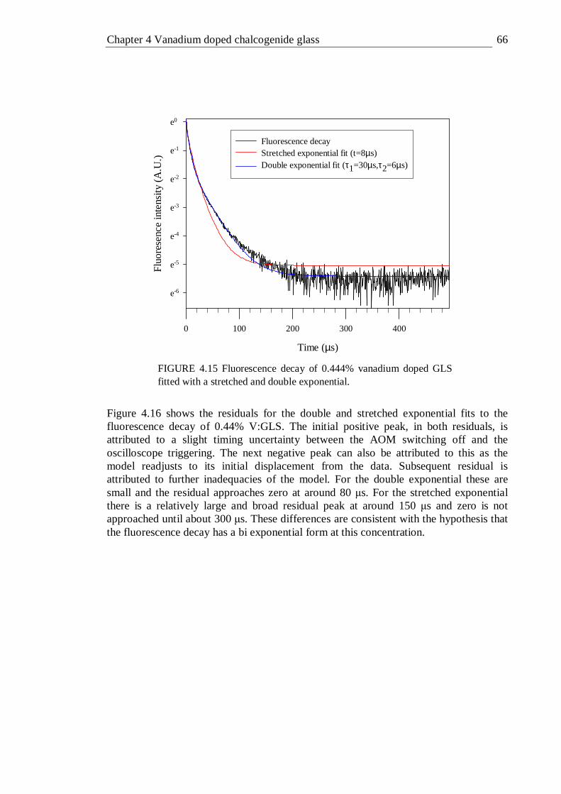
Chapter 4 Vanadium doped chalcogenide glass 66
Time (µs)
0 100 200 300 400
Flu
ores
enc
e in
tens
ity (
A.U
.)
e-6
e-5
e-4
e-3
e-2
e-1
e0
Fluorescence decayStretched exponential fit (t=8µs)Double exponential fit (τ1=30µs,τ2=6µs)
FIGURE 4.15 Fluorescence decay of 0.444% vanadium doped GLS fitted with a stretched and double exponential.
Figure 4.16 shows the residuals for the double and stretched exponential fits to the fluorescence decay of 0.44% V:GLS. The initial positive peak, in both residuals, is attributed to a slight timing uncertainty between the AOM switching off and the oscilloscope triggering. The next negative peak can also be attributed to this as the model readjusts to its initial displacement from the data. Subsequent residual is attributed to further inadequacies of the model. For the double exponential these are small and the residual approaches zero at around 80 µs. For the stretched exponential there is a relatively large and broad residual peak at around 150 µs and zero is not approached until about 300 µs. These differences are consistent with the hypothesis that the fluorescence decay has a bi exponential form at this concentration.
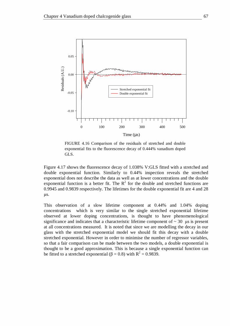
Chapter 4 Vanadium doped chalcogenide glass 67
Time (µs)
0 100 200 300 400 500
Re
sidu
als
(A.U
.)
-0.10
-0.05
0.00
0.05
Stretched exponential fitDouble exponential fit
FIGURE 4.16 Comparison of the residuals of stretched and double exponential fits to the fluorescence decay of 0.444% vanadium doped GLS.
Figure 4.17 shows the fluorescence decay of 1.038% V:GLS fitted with a stretched and double exponential function. Similarly to 0.44% inspection reveals the stretched exponential does not describe the data as well as at lower concentrations and the double exponential function is a better fit. The R2 for the double and stretched functions are 0.9945 and 0.9839 respectively. The lifetimes for the double exponential fit are 4 and 28 µs. This observation of a slow lifetime component at 0.44% and 1.04% doping concentrations which is very similar to the single stretched exponential lifetime observed at lower doping concentrations, is thought to have phenomenological significance and indicates that a characteristic lifetime component of ~ 30 µs is present at all concentrations measured. It is noted that since we are modelling the decay in our glass with the stretched exponential model we should fit this decay with a double stretched exponential. However in order to minimise the number of regressor variables, so that a fair comparison can be made between the two models, a double exponential is thought to be a good approximation. This is because a single exponential function can be fitted to a stretched exponential (β = 0.8) with R2 = 0.9839.
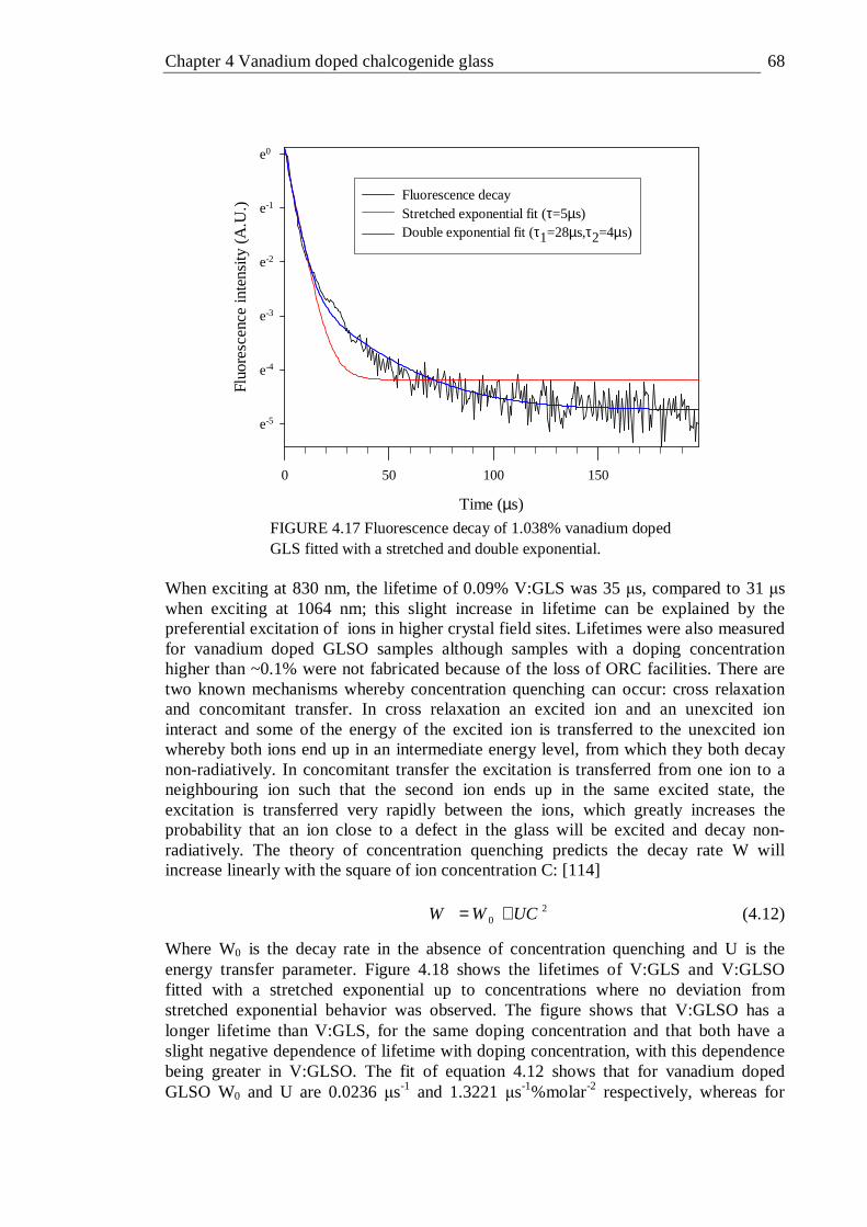
Chapter 4 Vanadium doped chalcogenide glass 68
Time (µs)
0 50 100 150
Flu
ore
sce
nce
inte
nsity
(A
.U.)
e-5
e-4
e-3
e-2
e-1
e0
Fluorescence decayStretched exponential fit (τ=5µs)Double exponential fit (τ1=28µs,τ2=4µs)
FIGURE 4.17 Fluorescence decay of 1.038% vanadium doped GLS fitted with a stretched and double exponential.
When exciting at 830 nm, the lifetime of 0.09% V:GLS was 35 µs, compared to 31 µs when exciting at 1064 nm; this slight increase in lifetime can be explained by the preferential excitation of ions in higher crystal field sites. Lifetimes were also measured for vanadium doped GLSO samples although samples with a doping concentration higher than ~0.1% were not fabricated because of the loss of ORC facilities. There are two known mechanisms whereby concentration quenching can occur: cross relaxation and concomitant transfer. In cross relaxation an excited ion and an unexcited ion interact and some of the energy of the excited ion is transferred to the unexcited ion whereby both ions end up in an intermediate energy level, from which they both decay non-radiatively. In concomitant transfer the excitation is transferred from one ion to a neighbouring ion such that the second ion ends up in the same excited state, the excitation is transferred very rapidly between the ions, which greatly increases the probability that an ion close to a defect in the glass will be excited and decay non-radiatively. The theory of concentration quenching predicts the decay rate W will increase linearly with the square of ion concentration C: [114]
20 UCWW += (4.12)
Where W0 is the decay rate in the absence of concentration quenching and U is the energy transfer parameter. Figure 4.18 shows the lifetimes of V:GLS and V:GLSO fitted with a stretched exponential up to concentrations where no deviation from stretched exponential behavior was observed. The figure shows that V:GLSO has a longer lifetime than V:GLS, for the same doping concentration and that both have a slight negative dependence of lifetime with doping concentration, with this dependence being greater in V:GLSO. The fit of equation 4.12 shows that for vanadium doped GLSO W0 and U are 0.0236 µs-1 and 1.3221 µs-1%molar-2 respectively, whereas for
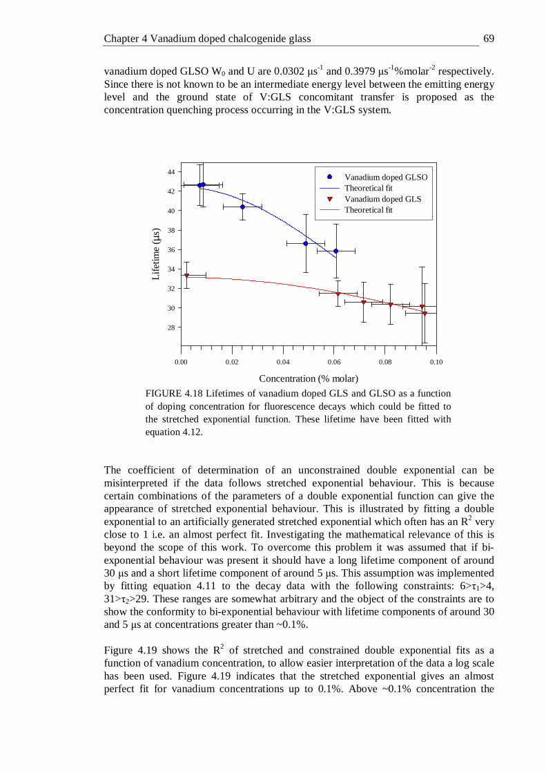
Chapter 4 Vanadium doped chalcogenide glass 69
vanadium doped GLSO W0 and U are 0.0302 µs-1 and 0.3979 µs-1%molar-2 respectively. Since there is not known to be an intermediate energy level between the emitting energy level and the ground state of V:GLS concomitant transfer is proposed as the concentration quenching process occurring in the V:GLS system.
Concentration (% molar)
0.00 0.02 0.04 0.06 0.08 0.10
Life
time
( µs)
28
30
32
34
36
38
40
42
44Vanadium doped GLSOTheoretical fitVanadium doped GLSTheoretical fit
FIGURE 4.18 Lifetimes of vanadium doped GLS and GLSO as a function of doping concentration for fluorescence decays which could be fitted to the stretched exponential function. These lifetime have been fitted with equation 4.12.
The coefficient of determination of an unconstrained double exponential can be misinterpreted if the data follows stretched exponential behaviour. This is because certain combinations of the parameters of a double exponential function can give the appearance of stretched exponential behaviour. This is illustrated by fitting a double exponential to an artificially generated stretched exponential which often has an R2 very close to 1 i.e. an almost perfect fit. Investigating the mathematical relevance of this is beyond the scope of this work. To overcome this problem it was assumed that if bi-exponential behaviour was present it should have a long lifetime component of around 30 µs and a short lifetime component of around 5 µs. This assumption was implemented by fitting equation 4.11 to the decay data with the following constraints: 6>τ1>4, 31>τ2>29. These ranges are somewhat arbitrary and the object of the constraints are to show the conformity to bi-exponential behaviour with lifetime components of around 30 and 5 µs at concentrations greater than ~0.1%. Figure 4.19 shows the R2 of stretched and constrained double exponential fits as a function of vanadium concentration, to allow easier interpretation of the data a log scale has been used. Figure 4.19 indicates that the stretched exponential gives an almost perfect fit for vanadium concentrations up to 0.1%. Above ~0.1% concentration the
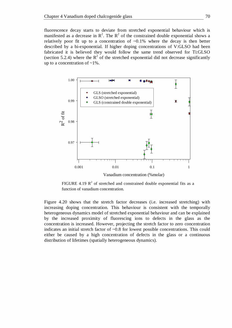
Chapter 4 Vanadium doped chalcogenide glass 70
fluorescence decay starts to deviate from stretched exponential behaviour which is manifested as a decrease in R2. The R2 of the constrained double exponential shows a relatively poor fit up to a concentration of ~0.1% where the decay is then better described by a bi-exponential. If higher doping concentrations of V:GLSO had been fabricated it is believed they would follow the same trend observed for Ti:GLSO (section 5.2.4) where the R2 of the stretched exponential did not decrease significantly up to a concentration of ~1%.
Vanadium concentration (%molar)
0.001 0.01 0.1 1
R2 o
f fit
0.97
0.98
0.99
1.00
GLS (stretched exponential)GLSO (stretched exponential)GLS (constrained double exponential)
FIGURE 4.19 R2 of stretched and constrained double exponential fits as a function of vanadium concentration.
Figure 4.20 shows that the stretch factor decreases (i.e. increased stretching) with increasing doping concentration. This behaviour is consistent with the temporally heterogeneous dynamics model of stretched exponential behaviour and can be explained by the increased proximity of fluorescing ions to defects in the glass as the concentration is increased. However, projecting the stretch factor to zero concentration indicates an initial stretch factor of ~0.8 for lowest possible concentrations. This could either be caused by a high concentration of defects in the glass or a continuous distribution of lifetimes (spatially heterogeneous dynamics).
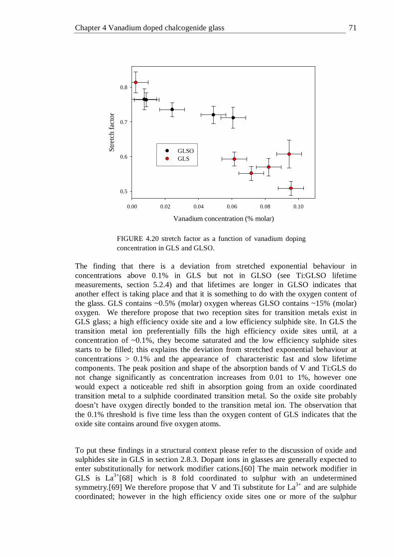
Chapter 4 Vanadium doped chalcogenide glass 71
Vanadium concentration (% molar)
0.00 0.02 0.04 0.06 0.08 0.10
Str
etc
h fa
cto
r
0.5
0.6
0.7
0.8
GLSOGLS
FIGURE 4.20 stretch factor as a function of vanadium doping concentration in GLS and GLSO.
The finding that there is a deviation from stretched exponential behaviour in concentrations above 0.1% in GLS but not in GLSO (see Ti:GLSO lifetime measurements, section 5.2.4) and that lifetimes are longer in GLSO indicates that another effect is taking place and that it is something to do with the oxygen content of the glass. GLS contains ~0.5% (molar) oxygen whereas GLSO contains ~15% (molar) oxygen. We therefore propose that two reception sites for transition metals exist in GLS glass; a high efficiency oxide site and a low efficiency sulphide site. In GLS the transition metal ion preferentially fills the high efficiency oxide sites until, at a concentration of ~0.1%, they become saturated and the low efficiency sulphide sites starts to be filled; this explains the deviation from stretched exponential behaviour at concentrations > 0.1% and the appearance of characteristic fast and slow lifetime components. The peak position and shape of the absorption bands of V and Ti:GLS do not change significantly as concentration increases from 0.01 to 1%, however one would expect a noticeable red shift in absorption going from an oxide coordinated transition metal to a sulphide coordinated transition metal. So the oxide site probably doesn’t have oxygen directly bonded to the transition metal ion. The observation that the 0.1% threshold is five time less than the oxygen content of GLS indicates that the oxide site contains around five oxygen atoms.
To put these findings in a structural context please refer to the discussion of oxide and sulphides site in GLS in section 2.8.3. Dopant ions in glasses are generally expected to enter substitutionally for network modifier cations.[60] The main network modifier in GLS is La3+[68] which is 8 fold coordinated to sulphur with an undetermined symmetry.[69] We therefore propose that V and Ti substitute for La3+ and are sulphide coordinated; however in the high efficiency oxide sites one or more of the sulphur
Chapter 4 Vanadium doped chalcogenide glass 72
atoms is part of an oxide negative cavity whereas in the low efficiency sulphide sites none, one or more of these sulphur atoms is part of a sulphide negative cavity. Two dopant reception sites have been reported for dysprosium doped GLS (Dy:GLS),[16] key differences with this work are that the lifetimes in Dy:GLSO and Dy:GLS were 100 µs and 2.54 ms respectively. This meant that the oxide site was low efficiency and the sulphide site was high efficiency. Separate absorption bands were also identified for the two sites. Dysprosium has the same outer electron structure as La; so if Dy substitutes for La the 8-fold coordination and any symmetry that may already exist would be expected to be maintained. However as a consequence of the outer electron structure and the relative size of V and Ti ions, tetrahedral and octahedral coordination are the most likely coordinations to occur. Analysis in this chapter indicates that vanadium is in a 2+ oxidation state and is octahedrally coordinated. So the addition of a transition metal to GLS will change the coordination of the La site it substitutes for from 8 to 6 or 4 (6 in the case of V:GLS) and bring about symmetry that may not have already existed. The oxide site being high efficiency for V:GLS and Ti:GLS, but low efficiency for Dy:GLS can be explained because O is more electronegative than S so the oxide site will have a slightly higher crystal field strength than the sulphide site. The separation of the lowest energy levels in transition metals is strongly influenced by crystal field strength so there will be a greater separation of the two lowest energy levels and therefore a lower probability of non-radiative decay. Energy levels in rare earths on the other hand are influenced very little by crystal field strength. The oxide site is expected to have a higher phonon energy than a sulphide site[16] this would increase the probability of non-radiative decay for both transition metal and rare-earth dopants. If the decrease in non-radiative decay caused by the increase in crystal field strength is greater than the increase in non-radiative decay caused by the increase in phonon energy for a transition metal in an oxide site then this would explain why the oxide site is high efficiency for transition metals and low efficiency for rare-earths. 4.8 Average Lifetime Because the fluorescence decay in this study has been modelled with both stretched and double exponential function, comparisons between the lifetimes are difficult. Because of this the average lifetime is used for comparison in this section. The average lifetime is the statistical average lifetime as used in population analysis, and can be thought of as the summation over all time of the number of members (excited ions in this case) lost in a time interval ∆t multiplied by their age at loss; this quantity is then averaged over the total population.[104] Equation 4.13 gives the average lifetime in integral form[85, 104, 115]
∫
∫=
=
=
==lim
lim
0
0
)(
)(
tt
t
tt
tav
dttI
dtttIτ (4.13)
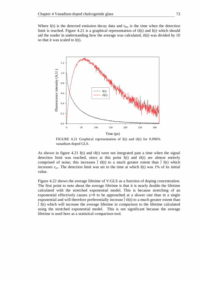
Chapter 4 Vanadium doped chalcogenide glass 73
Where I(t) is the detected emission decay data and tlim is the time when the detection limit is reached. Figure 4.21 is a graphical representation of tI(t) and I(t) which should aid the reader in understanding how the average was calculated, tI(t) was divided by 10 so that it was scaled to I(t).
Time (µs)
0 50 100 150 200 250 300
Flu
ore
sce
nce
inte
nsity
(A
.U.)
0.0
0.2
0.4
0.6
0.8
1.0
1.2
I(t)tI(t)
FIGURE 4.21 Graphical representation of I(t) and tI(t) for 0.096% vanadium doped GLS.
As shown in figure 4.21 I(t) and tI(t) were not integrated past a time when the signal detection limit was reached, since at this point I(t) and tI(t) are almost entirely comprised of noise; this increases ∫ tI(t) to a much greater extent than ∫ I(t) which increases τav. The detection limit was set to the time at which I(t) was 1% of its initial value. Figure 4.22 shows the average lifetime of V:GLS as a function of doping concentration. The first point to note about the average lifetime is that it is nearly double the lifetime calculated with the stretched exponential model. This is because stretching of an exponential effectively causes y=0 to be approached at a slower rate than in a single exponential and will therefore preferentially increase ∫ tI(t) to a much greater extent than ∫ I(t) which will increase the average lifetime in comparison to the lifetime calculated using the stretched exponential model. This is not significant because the average lifetime is used here as a statistical comparison tool.
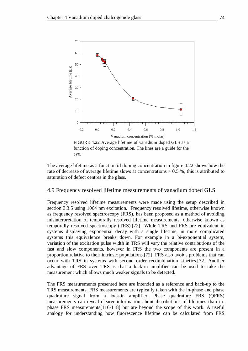
Chapter 4 Vanadium doped chalcogenide glass 74
Vanadium concentration (% molar)
-0.2 0.0 0.2 0.4 0.6 0.8 1.0 1.2
Ave
rage
life
time
( µs)
0
10
20
30
40
50
60
70
FIGURE 4.22 Average lifetime of vanadium doped GLS as a function of doping concentration. The lines are a guide for the eye.
The average lifetime as a function of doping concentration in figure 4.22 shows how the rate of decrease of average lifetime slows at concentrations > 0.5 %, this is attributed to saturation of defect centres in the glass. 4.9 Frequency resolved lifetime measurements of vanadium doped GLS Frequency resolved lifetime measurements were made using the setup described in section 3.3.5 using 1064 nm excitation. Frequency resolved lifetime, otherwise known as frequency resolved spectroscopy (FRS), has been proposed as a method of avoiding misinterpretation of temporally resolved lifetime measurements, otherwise known as temporally resolved spectroscopy (TRS).[72] While TRS and FRS are equivalent in systems displaying exponential decay with a single lifetime, in more complicated systems this equivalence breaks down. For example in a bi-exponential system, variation of the excitation pulse width in TRS will vary the relative contributions of the fast and slow components, however in FRS the two components are present in a proportion relative to their intrinsic populations.[72] FRS also avoids problems that can occur with TRS in systems with second order recombination kinetics.[72] Another advantage of FRS over TRS is that a lock-in amplifier can be used to take the measurement which allows much weaker signals to be detected. The FRS measurements presented here are intended as a reference and back-up to the TRS measurements. FRS measurements are typically taken with the in-phase and phase quadrature signal from a lock-in amplifier. Phase quadrature FRS (QFRS) measurements can reveal clearer information about distributions of lifetimes than in-phase FRS measurements[116-118] but are beyond the scope of this work. A useful analogy for understanding how fluorescence lifetime can be calculated from FRS

Chapter 4 Vanadium doped chalcogenide glass 75
measurements is to think of the fluorescing material as acting as a single RC time-constant filter with a cut-off frequency (υc) inversely proportional to the lifetime of the material. Hence the lifetime (τ) can be calculated from an in phase FRS measurement using equation 4.14.
cπυτ
2
1= (4.14)
Where the cut-off frequency υc is defined as the frequency in the stop-band at which the output power is half the output power in the pass-band (Ppass). The in phase FRS measurements for 0.0023%, 0.0944% and 1.038% V:GLS are shown in figure 4.23 along with the respective υc used to calculate the lifetime. The lifetimes calculated from FRS (τFRS) and TRS (τTRS) measurements are given in table 4.5. TABLE 4.5 Lifetimes of various concentrations of V:GLS, calculated by FRS and TRS. † TRS lifetime calculated from stretched exponential fit (excited at 1064 nm), ‡ TRS lifetime calculated from average lifetime (excited at 1064 nm). †† 633 nm excitation.
Vanadium concentration (%molar) υc(KHz) τFRS (µs) τTRS (µs) 0.0023 4.8429 32.86 33.34†
0.0944 5.0441 31.55 30.15† 1.038 16.5015 9.64 11.10‡ 0.0944 5.014 31.86†† -
The lifetimes calculated by FRS are in excellent agreement with TRS lifetimes calculated using the stretched exponential function; this validates the use of the stretched exponential function in calculating the fluorescence lifetime. The FRS lifetime measurement for 1.038% V:GLS is in reasonably good agreement with the average lifetime. The lifetime measured using a 1 mW 633 nm laser excitation source is in excellent agreement with the lifetime measured at 1064 nm in table 4.5. TRS measurement was not possible at 633 nm excitation because of the relatively low emission intensity at this wavelength (see V:GLS PLE figure 4.12) and the low power available; this highlights the advantage of FRS over TRS measurements. The lifetimes of 0.0944% V:GLS measured at wavelengths of 633, 830 and 1064 nm were 32, 35 and 30 µs respectively, see table 4.5 and section 4.7. Excitation at these wavelengths roughly equates to excitation into each of the three observed absorption bands and the observation of the same characteristic lifetime indicates that the three absorption bands all belong to the same oxidation state of vanadium.
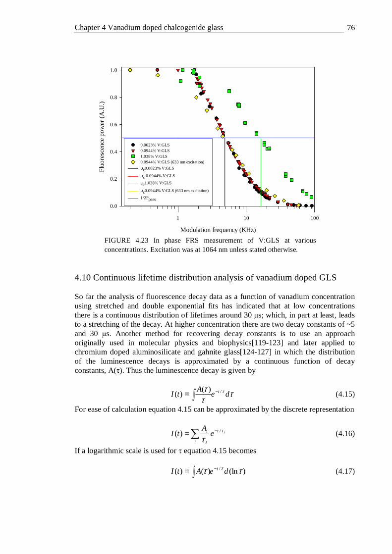
Chapter 4 Vanadium doped chalcogenide glass 76
Modulation frequency (KHz)
1 10 100
Flu
ore
scen
ce p
ow
er (
A.U
.)
0.0
0.2
0.4
0.6
0.8
1.0
0.0023% V:GLS0.0944% V:GLS1.038% V:GLS0.0944% V:GLS (633 nm excitation)
υc0.0023% V:GLS
υc 0.0944% V:GLS
uc1.038% V:GLS
υc0.0944% V:GLS (633 nm excitation)
1/2Ppass
FIGURE 4.23 In phase FRS measurement of V:GLS at various concentrations. Excitation was at 1064 nm unless stated otherwise.
4.10 Continuous lifetime distribution analysis of vanadium doped GLS So far the analysis of fluorescence decay data as a function of vanadium concentration using stretched and double exponential fits has indicated that at low concentrations there is a continuous distribution of lifetimes around 30 µs; which, in part at least, leads to a stretching of the decay. At higher concentration there are two decay constants of ~5 and 30 µs. Another method for recovering decay constants is to use an approach originally used in molecular physics and biophysics[119-123] and later applied to chromium doped aluminosilicate and gahnite glass[124-127] in which the distribution of the luminescence decays is approximated by a continuous function of decay constants, A(τ). Thus the luminescence decay is given by
τττ τ de
AtI t /)()( −∫= (4.15)
For ease of calculation equation 4.15 can be approximated by the discrete representation
∑ −=i
t
i
i ieA
tI τ
τ/)( (4.16)
If a logarithmic scale is used for τ equation 4.15 becomes
)(ln)()( / ττ τ deAtI t−∫= (4.17)
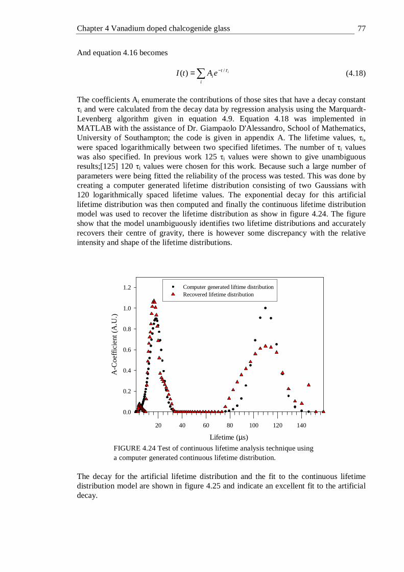
Chapter 4 Vanadium doped chalcogenide glass 77
And equation 4.16 becomes
∑ −=i
ti
ieAtI τ/)( (4.18)
The coefficients Ai enumerate the contributions of those sites that have a decay constant τi and were calculated from the decay data by regression analysis using the Marquardt-Levenberg algorithm given in equation 4.9. Equation 4.18 was implemented in MATLAB with the assistance of Dr. Giampaolo D'Alessandro, School of Mathematics, University of Southampton; the code is given in appendix A. The lifetime values, τi, were spaced logarithmically between two specified lifetimes. The number of τi values was also specified. In previous work 125 τi values were shown to give unambiguous results;[125] 120 τi values were chosen for this work. Because such a large number of parameters were being fitted the reliability of the process was tested. This was done by creating a computer generated lifetime distribution consisting of two Gaussians with 120 logarithmically spaced lifetime values. The exponential decay for this artificial lifetime distribution was then computed and finally the continuous lifetime distribution model was used to recover the lifetime distribution as show in figure 4.24. The figure show that the model unambiguously identifies two lifetime distributions and accurately recovers their centre of gravity, there is however some discrepancy with the relative intensity and shape of the lifetime distributions.
Lifetime (µs)
20 40 60 80 100 120 140
A-C
oef
ficie
nt (
A.U
.)
0.0
0.2
0.4
0.6
0.8
1.0
1.2 Computer generated liftime distributionRecovered lifetime distribution
FIGURE 4.24 Test of continuous lifetime analysis technique using a computer generated continuous lifetime distribution.
The decay for the artificial lifetime distribution and the fit to the continuous lifetime distribution model are shown in figure 4.25 and indicate an excellent fit to the artificial decay.
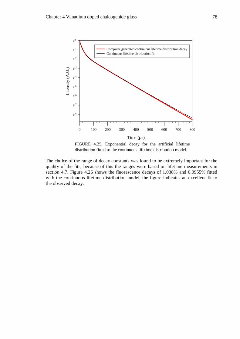
Chapter 4 Vanadium doped chalcogenide glass 78
Time (µs)
0 100 200 300 400 500 600 700 800
Inte
nsity
(A
.U.)
e-8
e-7
e-6
e-5
e-4
e-3
e-2
e-1
e0
Computer generated continuous lifetime distribution decayContinuous lifetime distribution fit
FIGURE 4.25. Exponential decay for the artificial lifetime distribution fitted to the continuous lifetime distribution model.
The choice of the range of decay constants was found to be extremely important for the quality of the fits, because of this the ranges were based on lifetime measurements in section 4.7. Figure 4.26 shows the fluorescence decays of 1.038% and 0.0955% fitted with the continuous lifetime distribution model, the figure indicates an excellent fit to the observed decay.

Chapter 4 Vanadium doped chalcogenide glass 79
Time (µs)
0 50 100 150 200 250
Em
issi
on
inte
nsity
(A
.U.)
e-5
e-4
e-3
e-2
e-1
e0
1.038% V:GLS fluorescence decayContinuous lifetime distribution fit0.0955% V:GLS fluorescence decayContinuous lifetime distribution fit
FIGURE 4.26 Some fluorescence decays of V:GLS fitted with a continuous lifetime distribution.
Figure 4.27 shows how the distribution of lifetimes varies with vanadium concentration. The figure shows that at the lowest concentration there is a single distribution of lifetimes with a centre of gravity around 35 µs, which is in good agreement with the lifetime calculated from stretched exponential fit of 33.4 µs. As the concentration increases, two distribution peaks become apparent, one centred around 30 µs (peak 1) and another around 5 µs (peak 2). It is also clear that, as the concentration increases, peak 2 becomes more intense in comparison to peak 1. The distribution of lifetimes also appears to be narrower in peak 2. Since the centre of gravity of the lifetime distribution peaks can not be identified precisely from figure 4.27 they are given in table 4.6 along with lifetimes calculated from double and stretched exponential fits. Table 4.6 shows that there is excellent agreement between the lifetime distribution peaks and the stretched and double exponential peaks. The lifetime distributions also verify the assignment of double exponential behaviour at concentrations > ~0.1. However the lifetime distribution for 0.0955% V:GLS, which was found to be better described by a stretched than a double exponential, shows that a lifetime component ~ 5 µs is present although this component is small in comparison to the distribution ~ 30 µs.

Chapter 4 Vanadium doped chalcogenide glass 80
0.0
0.2
0.4
0.6
0.8
1.0
10
20
30
40
5060
0.00.2
0.40.6
0.81.0
A-C
oeff
icie
nt (
A.U
.)
Life
time (
µ s)
Vanadium concentration (% molar)
1.038%0.4443%0.0955%0.0023%
Figure 4.27 Lifetime distribution in V:GLS at various vanadium concentrations.
TABLE 4.6 Lifetimes identified by continuous lifetime distribution, double exponential and stretched exponential fits to the fluorescence decay of V:GLS at various vanadium concentrations.
Vanadium concentration
(%molar)
Continuous lifetime
distribution peak 1 (µs)
Continuous lifetime
distribution peak 2 (µs)
Double exponential fit τ1 (µs)
Double exponential fit τ2 (µs)
Stretched exponential
fit (µs)
0.0023 34.9 - - - 33.34
0.0944 30.0 4.8 - - 30.15 0.4443 26.5 5.5 28.8 5.9 - 1.038 26.3 4.4 28.3 4.4 -
.
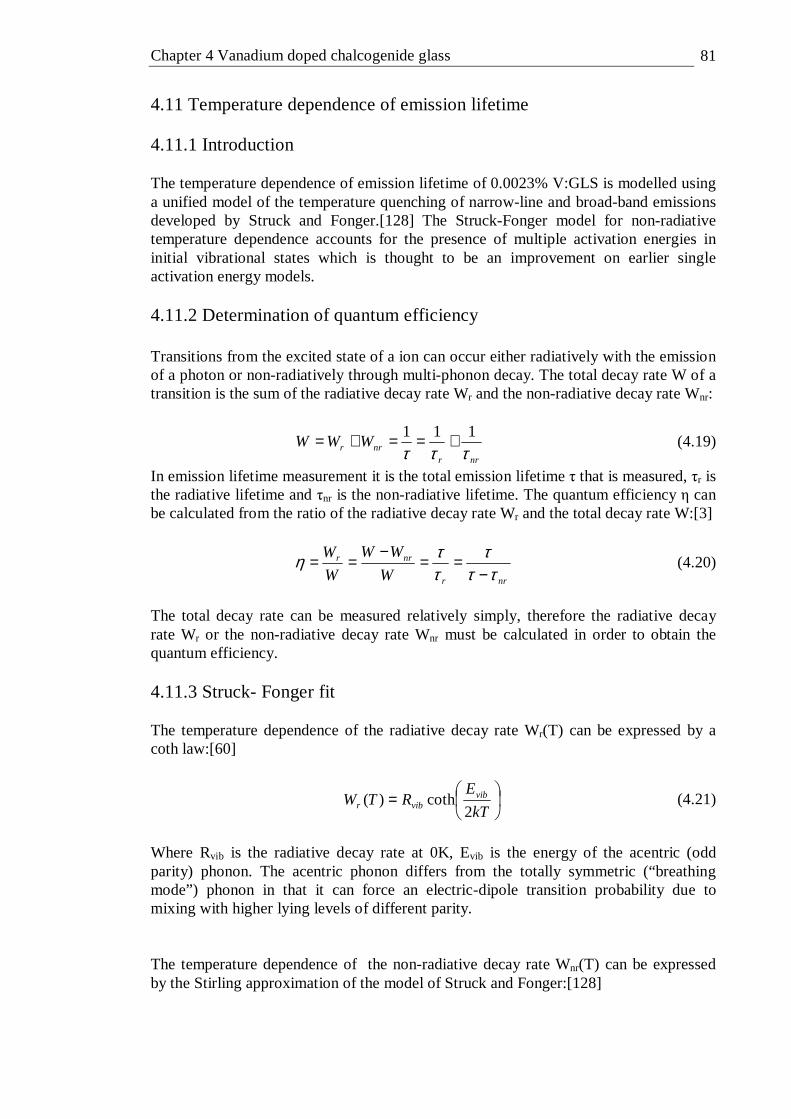
Chapter 4 Vanadium doped chalcogenide glass 81
4.11 Temperature dependence of emission lifetime 4.11.1 Introduction The temperature dependence of emission lifetime of 0.0023% V:GLS is modelled using a unified model of the temperature quenching of narrow-line and broad-band emissions developed by Struck and Fonger.[128] The Struck-Fonger model for non-radiative temperature dependence accounts for the presence of multiple activation energies in initial vibrational states which is thought to be an improvement on earlier single activation energy models. 4.11.2 Determination of quantum efficiency Transitions from the excited state of a ion can occur either radiatively with the emission of a photon or non-radiatively through multi-phonon decay. The total decay rate W of a transition is the sum of the radiative decay rate Wr and the non-radiative decay rate Wnr:
nrrnrr WWW
τττ111 +==+= (4.19)
In emission lifetime measurement it is the total emission lifetime τ that is measured, τr is the radiative lifetime and τnr is the non-radiative lifetime. The quantum efficiency η can be calculated from the ratio of the radiative decay rate Wr and the total decay rate W:[3]
nrr
nrr
W
WW
W
W
τττ
ττη
−==
−== (4.20)
The total decay rate can be measured relatively simply, therefore the radiative decay rate Wr or the non-radiative decay rate Wnr must be calculated in order to obtain the quantum efficiency. 4.11.3 Struck- Fonger fit The temperature dependence of the radiative decay rate Wr(T) can be expressed by a coth law:[60]
=kT
ERTW vib
vibr 2coth)( (4.21)
Where Rvib is the radiative decay rate at 0K, Evib is the energy of the acentric (odd parity) phonon. The acentric phonon differs from the totally symmetric (“breathing mode”) phonon in that it can force an electric-dipole transition probability due to mixing with higher lying levels of different parity. The temperature dependence of the non-radiative decay rate Wnr(T) can be expressed by the Stirling approximation of the model of Struck and Fonger:[128]
Chapter 4 Vanadium doped chalcogenide glass 82
pp
mSnrnr pp
mS
p
eeRW
++
= +−**
12 12
2
*
π (4.22)
Where
mmSpp ++= 14 22* ,
1
1/ −
=kTe
m ωh ,
Where S is the Huang-Rhys parameter, which describes the amount of overlap between the ground and excited state parabola, p is the number of phonons bridging the energy gap, Rnr is the non-radiative decay constant and hω is the energy of the effective symmetric phonon. This approximation is valid for P*>1. At 0K <m> → 0, therefore Wnr at 0K is given by:
pSp
nrnr p
S
p
eRW
=
−
π2)0( (4.23)
Hence equation (4.22) can now be expressed in a form which is used to fit to the experimental data:
( )mSpp
p
nrnr epp
mp
p
pWTW 2
*
2/1
*
*12)0()( −−
++
= (4.24)
The total decay rate is thus given by:
),,,(),( pSRWERWWWW nrnrvibvibrnrr ωh+=+=
( )mSpp
ppSp
nrvib
vib epp
mp
p
p
p
S
p
eR
kT
ER 2
*
2/1
*
*12
22coth −−
−
++
+
=π
(4.25)
This equation can now be fitted to the measured experimental data (the total decay rate W as a function of temperature) in order to find fit parameters to calculate the radiative decay rate Wr and hence calculate the quantum efficiency. 4.11.4 Parameter estimation In order to achieve a valid fit to the experimental data, initial estimates of the start values of the fit parameters need to be made as accurately as possible. The Huang-Rhys parameter, S, and the acentric phonon energy, Evib, can be estimated from the temperature dependence of emission bandwidths Γ(T):[60]
2/1
2coth36.2)(
=ΓkT
EST vibωh (4.26)

Chapter 4 Vanadium doped chalcogenide glass 83
Temperature dependent emission bandwidth measurements were taken using the photoluminescence spectroscopy setup described in section 3.3.2 but with the 0.0023% V:GLS sample enclosed in a Leybold AG helium gas closed cycle cryostat. When the cryostat reached the desired temperature it was left at that temperature for 40 minutes to allow for any thermal inertia between the temperature sensor and the sample. The excitation source was a CW 1064nm Nd:YAG laser with approximately 0.5 Watt output power. Emission was detected with an EG&G optoelectronics J10D liquid nitrogen cooled InSb detector. Figure 4.28 shows the spectra plotted in energy taken at temperatures varying from 6.6 K to 293 K. These spectra where fitted to the 4 parameter Gaussian in equation 4.2.
FIGURE 4.28 Emission spectra of 0.0023% V:GLS at various temperatures fitted with a 4 parameter Gaussian.
The variation in FWHM of the Gaussian curves in figure 4.28 was less than the estimated resolution of approximately 60 cm-1. This indicates that emission broadening due to an inhomogeneous broadening mechanism, such as the range of crystal field strengths (Dq) that can be created in different glass sites,[129] is much stronger than that caused by the coupling of vibrational modes. The S and Evib parameters cannot therefore be estimated using this method. The resolution was estimated to be approximately 60 cm-1 by averaging the difference between bandwidth measurements taken at the same temperature. The accuracy of this experiment was hampered by noise from the detector caused by vibration of the closed cycle cryostat. Several methods of isolating the detector from the vibration were tried but none succeeded in eliminating the vibration.
Chapter 4 Vanadium doped chalcogenide glass 84
The Huang-Rhys parameter S can also be calculated from the emission bandwidth at 0K:[60]
2/136.2)0( Sωh=Γ (4.27) The bandwidth measured at 6.6K was measured to be 1740 cm-1 and is a good approximation for the 0K bandwidth (Γ(0)). The maximum phonon energy, hω, has been measured previously[34] to be 425 cm-1. This gives an estimate for the S parameter of 2.95. If the ground and excited state parabola are identical the Huang-Rhys parameter S can also be calculated from the difference between the emission and absorption band peaks (known as the Stokes shift (SS)) and the maximum phonon energy hω:[60] SS=(2S-1) hω. A description of the Huang-Rhys parameter and Stokes shift in terms of the single configurational coordinate model is given in section 2.5. The 300K absorption peak at 9091 cm-1 and an emission peak at 6725 cm-1 gives a Stokes shift of 2366 cm-1. This gives an estimate of the S parameter of 3.28, the difference to the 0K emission bandwidth calculation may be because the ground and excited state parabola are not identical. The number of phonons bridging the energy gap Egap can be calculated from p=Egap/hω. Egap for V:GLS is 6725 cm-1 which gives p=15.82. Assuming that Evib is equal to the maximum phonon energy hω, the radiative rate at 0 K can be estimated:[130]
==
kT
ET
T
KKR
vibrvib
2coth)(
)(
)0(
1)0(
τ
ητ
(4.28)
Then using the quantum efficiency for V:GLS at 300 K of 0.04 calculated in section 4.12 and the lifetime at 300 K of 33 µs, Rvib(0K)=Wr(0K) was estimated to be 936 s-1. Approximating W(0K) to 1/τ(6.5K) and using equation 4.19, Wnr(0K) ≈ 18290 s-1 . Using equation 4.23 with S=2.95, Wnr(0K)=8290 s-1 and p=15.82 the non-radiative decay constant Rnr is 9x10¹⁰ s-1. 4.11.5 Temperature dependent lifetime measurements Temperature dependent lifetime measurements were taken using the fluorescence lifetime setup described in section 3.3.4, except with the sample enclosed in a Leybold AG helium gas closed cycle cryostat. Fluorescence was detected by a new focus 2034 extended InGaS detector. The excitation source was a 1064nm Nd:YAG laser with the output power attenuated to approximately 10 mW. When the cryostat reached the desired temperature it was left at that temperature for 40 minutes to allow for any thermal inertia between the temperature sensor and the sample. The emission decay curves, for various temperatures between 6.6 K and 293 K are shown in figure 4.29 together with the stretched exponential fits that were used to calculate the 1/e lifetimes.

Chapter 4 Vanadium doped chalcogenide glass 85
Time (µs)
0 200 400 600 800
Flu
ore
scen
ce I
nten
sity
(A
.U.)
e-7
e-6
e-5
e-4
e-3
e-2
e-1
e0
Fluorescence decay (6.5 K)Fluorescence decay (300 K)Stretched exponential fit (τ= 33.3µs)Stretched exponential fit (τ= 54.5µs)
FIGURE 4.29 Emission decay of 0.0023% V:GLS at 6.5 and 300 K together with stretched exponential fits.
The experimental data was fitted to equation 4.25 with the parameters estimated previously as initial parameters. All of the parameters were fitted to the data except hω which has previously been determined experimentally and was set as a constant. The initial and fitted parameters are given in table 4.7. Figure 4.30 shows the experimentally determined decay rates, the Struck-Fonger fit and the non-radiative decay rate, Wnr(T), calculated from the fitted parameters Rnr, hω, S and p with equation 4.24. The figure indicates that the Struck-Fonger model describes the temperature dependent decay rate of V:GLS very well from 300-210 K but then there is a small deviation that can not be accounted for by the model, this may be related to the disordered nature of the glass host. It can also be seen that at 0 K there are still strong non-radiative processes occurring.

Chapter 4 Vanadium doped chalcogenide glass 86
. Temperature (K)
50 100 150 200 250 300
Dec
ay
rate
(s-1
)
18000
20000
22000
24000
26000
28000
30000
Measured decay rateCalculated non-radiative decay rateStruck-Fonger fit
FIGURE 4.30 Experimental data for the total decay rate of 0.0023% vanadium doped GLS as a function of temperature fitted to the model of Struck and Fonger and the non-radiative decay rate as a function of temperature was calculated from the fit parameters.
In figure 4.31 the quantum efficiency (QE) as a function of temperature η(T) was calculated from experimentally measured total decay rate as a function of temperature W(T) and the non-radiative decay rate as a function of temperature Wnr(T) with: η(T)= W(T)-Wnr(T)/ W(T). The fit shows a 5.1% QE at room temperature which is in excellent agreement with the spectroscopically determined QE of 4.2%. Errors in the calculated QE were estimated from the coefficient of determination of the Struck-Fonger fit.
TABLE 4.7 Initial estimate and fit parameters for Struck-Fonger fit.
Rvib (s-1) Evib(cm-1) Rnr (s
-1) hω (cm-1) S p Initial estimate 936 425 9x10¹⁰ 425cm-1 2.95 15.82
Struck-Fonger fit 4549 1414 7.9x10¹⁰ - 2.79 15.05
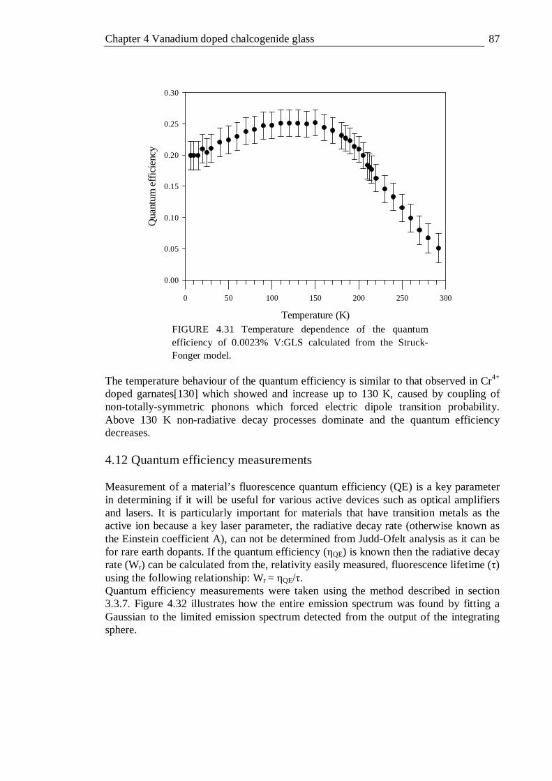
Chapter 4 Vanadium doped chalcogenide glass 87
Temperature (K)
0 50 100 150 200 250 300
Qua
ntum
effi
cie
ncy
0.00
0.05
0.10
0.15
0.20
0.25
0.30
FIGURE 4.31 Temperature dependence of the quantum efficiency of 0.0023% V:GLS calculated from the Struck-Fonger model.
The temperature behaviour of the quantum efficiency is similar to that observed in Cr4+ doped garnates[130] which showed and increase up to 130 K, caused by coupling of non-totally-symmetric phonons which forced electric dipole transition probability. Above 130 K non-radiative decay processes dominate and the quantum efficiency decreases.
4.12 Quantum efficiency measurements Measurement of a material’s fluorescence quantum efficiency (QE) is a key parameter in determining if it will be useful for various active devices such as optical amplifiers and lasers. It is particularly important for materials that have transition metals as the active ion because a key laser parameter, the radiative decay rate (otherwise known as the Einstein coefficient A), can not be determined from Judd-Ofelt analysis as it can be for rare earth dopants. If the quantum efficiency (ηQE) is known then the radiative decay rate (Wr) can be calculated from the, relativity easily measured, fluorescence lifetime (τ) using the following relationship: Wr = ηQE/τ. Quantum efficiency measurements were taken using the method described in section 3.3.7. Figure 4.32 illustrates how the entire emission spectrum was found by fitting a Gaussian to the limited emission spectrum detected from the output of the integrating sphere.

Chapter 4 Vanadium doped chalcogenide glass 88
Wavelength (nm)
1200 1400 1600 1800 2000 2200
Inte
nsity
(A
.U.)
0.5
1.0
1.5
2.0
2.5
3.0 Detected emission spectrumGaussian fit
FIGURE 4.32 Emission spectrum of 0.0023% V:GLS taken with an integrating sphere and fitted to a Gaussian.
Appendix B gives the area under all the spectra taken, together with the calculated quantum efficiencies. The quantum efficiency for the vanadium doped GLS samples are illustrated in figure 4.33 including the experimental error bounds. The quantum efficiency as a function of vanadium doping concentration follows a similar trend to the lifetime i.e. decreasing with increasing doping concentration. However whereas the lifetime in V:GLSO was higher than V:GLS for the same vanadium concentration it appears that the quantum efficiency is the same or slightly lower in V:GLSO for the same doping concentration. This means that in V:GLSO the radiative rate is lower than in V:GLS since Wr = Wη, where η is the quantum efficiency. The decrease in QE with increasing concentration can be attributed to increased re-absorption of the emission and/or increased concentration quenching.

Chapter 4 Vanadium doped chalcogenide glass 89
Vanadium concentration (% molar)
0.00 0.02 0.04 0.06 0.08 0.10
Qua
ntum
Effi
cie
ncy
0.00
0.01
0.02
0.03
0.04
0.05
GLSGLSO
FIGURE 4.33 Quantum efficiency of vanadium doped GLS as a function of doping concentration measured with an integrating sphere.
The formula of McCumber,[131] in equation 4.29, is used to calculate the peak emission cross section.
λλ
ππσ
∆=
40
24
2ln
cn
Aem (4.29)
Where λ0 is the peak fluorescence wavelength, ∆λ is the FWHM, n is the refractive index, c is the speed of light and A is the Einstein coefficient (also known as the radiative rate (Wr)) and is calculated from: A = QE/τ. The peak emission cross-sections, calculated for various concentrations of V:GLS and V:GLS, are given in table 4.9. TABLE 4.9 Details of vanadium samples with their respective quantum efficiency, peak emission wavelength (λmax), emission bandwidths (∆λ), emission lifetimes (τ), emission cross sections (σem) and σemτ products at room temperature.
Vanadium concentration
(%molar)
Host Sample dimensions
(mm)
QE (%)
λmax (nm)
∆λ (nm)
τ (µs) σem (10-21 cm2)
σemτ (10-
26scm2) 0.0023 GLS 8x5x4 4.19 1470 484 33.35 2.721 9.08 0.0616 GLS 8x5x3 2.08 1508 447 31.47 1.716 5.40 0.0944 GLS 8x8x0.5 1.56 1536 462 30.15 1.579 4.76 0.0087 GLSO 8x8x0.5 3.43 1461 450 42.68 2.051 8.75 0.0242 GLSO 8x8x0.5 2.93 1466 448 40.39 1.886 7.62 0.0489 GLSO 8x8x0.5 1.86 1477 467 36.60 1.306 4.78 0.0608 GLSO 8x8x0.5 1.42 1482 447 35.84 1.078 3.86
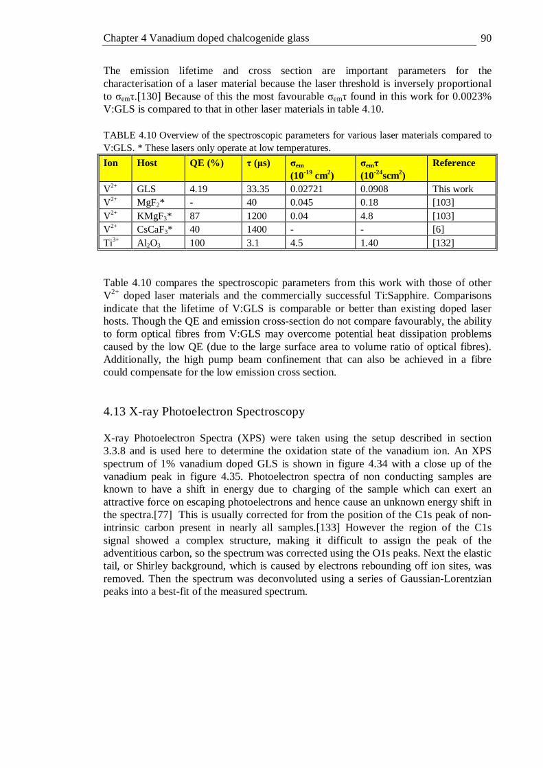
Chapter 4 Vanadium doped chalcogenide glass 90
The emission lifetime and cross section are important parameters for the characterisation of a laser material because the laser threshold is inversely proportional to σemτ.[130] Because of this the most favourable σemτ found in this work for 0.0023% V:GLS is compared to that in other laser materials in table 4.10. TABLE 4.10 Overview of the spectroscopic parameters for various laser materials compared to V:GLS. * These lasers only operate at low temperatures.
Ion Host QE (%) τ (µs) σem (10-19 cm2)
σemτ (10-24scm2)
Reference
V2+ GLS 4.19 33.35 0.02721 0.0908 This work V2+ MgF2* - 40 0.045 0.18 [103] V2+ KMgF3* 87 1200 0.04 4.8 [103] V2+ CsCaF3* 40 1400 - - [6] Ti3+ Al2O3 100 3.1 4.5 1.40 [132]
Table 4.10 compares the spectroscopic parameters from this work with those of other V2+ doped laser materials and the commercially successful Ti:Sapphire. Comparisons indicate that the lifetime of V:GLS is comparable or better than existing doped laser hosts. Though the QE and emission cross-section do not compare favourably, the ability to form optical fibres from V:GLS may overcome potential heat dissipation problems caused by the low QE (due to the large surface area to volume ratio of optical fibres). Additionally, the high pump beam confinement that can also be achieved in a fibre could compensate for the low emission cross section.
4.13 X-ray Photoelectron Spectroscopy X-ray Photoelectron Spectra (XPS) were taken using the setup described in section 3.3.8 and is used here to determine the oxidation state of the vanadium ion. An XPS spectrum of 1% vanadium doped GLS is shown in figure 4.34 with a close up of the vanadium peak in figure 4.35. Photoelectron spectra of non conducting samples are known to have a shift in energy due to charging of the sample which can exert an attractive force on escaping photoelectrons and hence cause an unknown energy shift in the spectra.[77] This is usually corrected for from the position of the C1s peak of non-intrinsic carbon present in nearly all samples.[133] However the region of the C1s signal showed a complex structure, making it difficult to assign the peak of the adventitious carbon, so the spectrum was corrected using the O1s peaks. Next the elastic tail, or Shirley background, which is caused by electrons rebounding off ion sites, was removed. Then the spectrum was deconvoluted using a series of Gaussian-Lorentzian peaks into a best-fit of the measured spectrum.
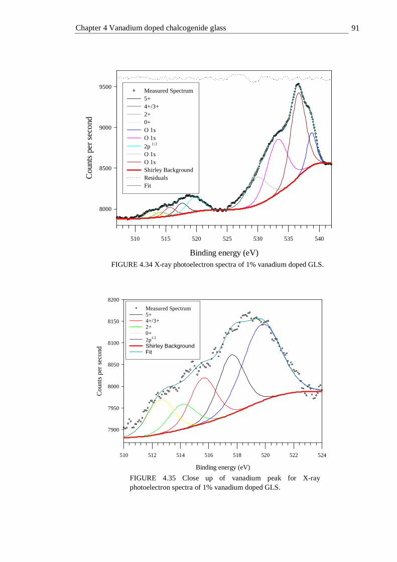
Chapter 4 Vanadium doped chalcogenide glass 91
Binding energy (eV)
510 515 520 525 530 535 540
Cou
nts
per
seco
nd
8000
8500
9000
9500Measured Spectrum 5+ 4+/3+ 2+ 0+ O 1s O 1s
2p 1/2 O 1s O 1s Shirley Background Residuals Fit
FIGURE 4.34 X-ray photoelectron spectra of 1% vanadium doped GLS.
Binding energy (eV)
510 512 514 516 518 520 522 524
Cou
nts
per
seco
nd
7900
7950
8000
8050
8100
8150
8200
Measured Spectrum 5+ 4+/3+ 2+ 0+ 2p1/2
Shirley Background Fit
FIGURE 4.35 Close up of vanadium peak for X-ray photoelectron spectra of 1% vanadium doped GLS.
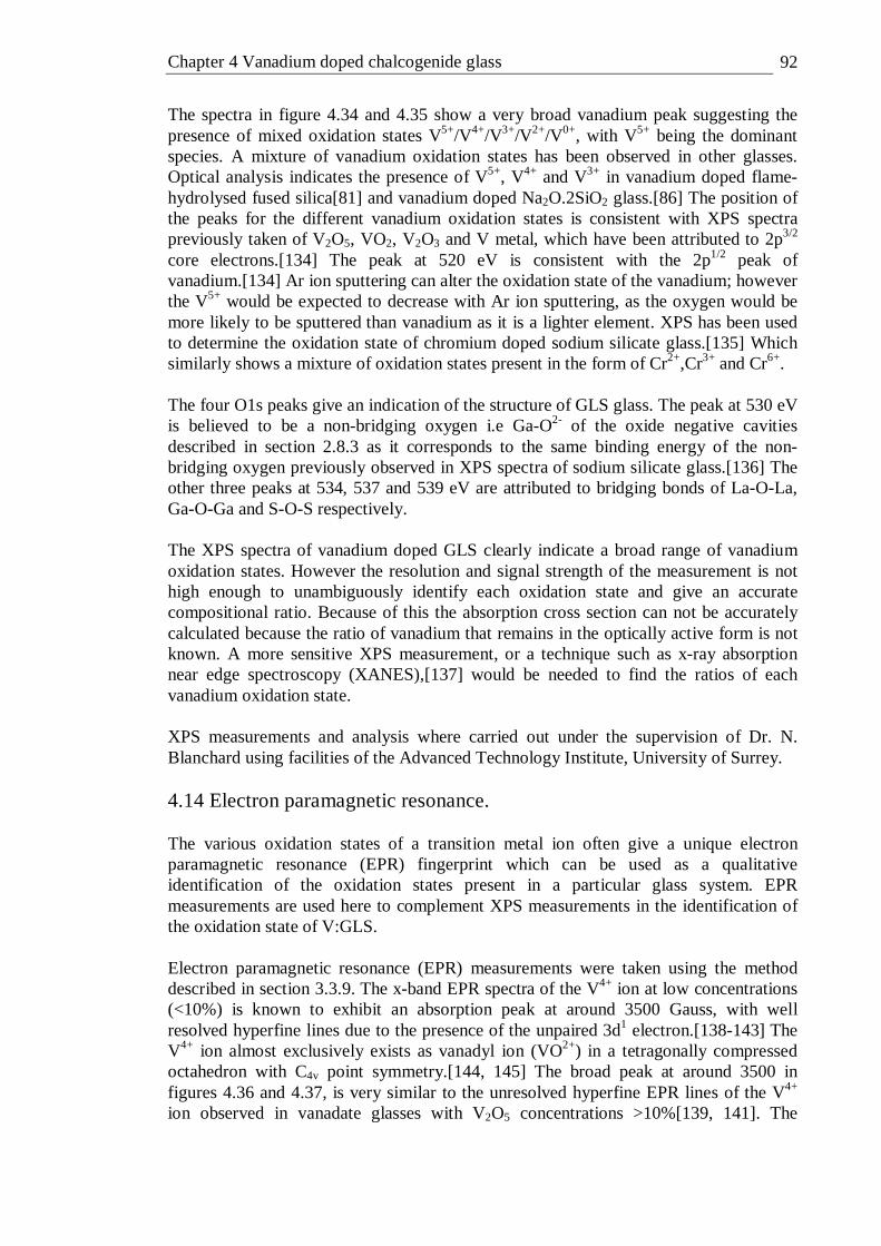
Chapter 4 Vanadium doped chalcogenide glass 92
The spectra in figure 4.34 and 4.35 show a very broad vanadium peak suggesting the presence of mixed oxidation states V5+/V4+/V3+/V2+/V0+, with V5+ being the dominant species. A mixture of vanadium oxidation states has been observed in other glasses. Optical analysis indicates the presence of V5+, V4+ and V3+ in vanadium doped flame-hydrolysed fused silica[81] and vanadium doped Na2O.2SiO2 glass.[86] The position of the peaks for the different vanadium oxidation states is consistent with XPS spectra previously taken of V2O5, VO2, V2O3 and V metal, which have been attributed to 2p3/2 core electrons.[134] The peak at 520 eV is consistent with the 2p1/2 peak of vanadium.[134] Ar ion sputtering can alter the oxidation state of the vanadium; however the V5+ would be expected to decrease with Ar ion sputtering, as the oxygen would be more likely to be sputtered than vanadium as it is a lighter element. XPS has been used to determine the oxidation state of chromium doped sodium silicate glass.[135] Which similarly shows a mixture of oxidation states present in the form of Cr2+,Cr3+ and Cr6+. The four O1s peaks give an indication of the structure of GLS glass. The peak at 530 eV is believed to be a non-bridging oxygen i.e Ga-O2- of the oxide negative cavities described in section 2.8.3 as it corresponds to the same binding energy of the non-bridging oxygen previously observed in XPS spectra of sodium silicate glass.[136] The other three peaks at 534, 537 and 539 eV are attributed to bridging bonds of La-O-La, Ga-O-Ga and S-O-S respectively. The XPS spectra of vanadium doped GLS clearly indicate a broad range of vanadium oxidation states. However the resolution and signal strength of the measurement is not high enough to unambiguously identify each oxidation state and give an accurate compositional ratio. Because of this the absorption cross section can not be accurately calculated because the ratio of vanadium that remains in the optically active form is not known. A more sensitive XPS measurement, or a technique such as x-ray absorption near edge spectroscopy (XANES),[137] would be needed to find the ratios of each vanadium oxidation state. XPS measurements and analysis where carried out under the supervision of Dr. N. Blanchard using facilities of the Advanced Technology Institute, University of Surrey.
4.14 Electron paramagnetic resonance. The various oxidation states of a transition metal ion often give a unique electron paramagnetic resonance (EPR) fingerprint which can be used as a qualitative identification of the oxidation states present in a particular glass system. EPR measurements are used here to complement XPS measurements in the identification of the oxidation state of V:GLS. Electron paramagnetic resonance (EPR) measurements were taken using the method described in section 3.3.9. The x-band EPR spectra of the V4+ ion at low concentrations (<10%) is known to exhibit an absorption peak at around 3500 Gauss, with well resolved hyperfine lines due to the presence of the unpaired 3d1 electron.[138-143] The V4+ ion almost exclusively exists as vanadyl ion (VO2+) in a tetragonally compressed octahedron with C4v point symmetry.[144, 145] The broad peak at around 3500 in figures 4.36 and 4.37, is very similar to the unresolved hyperfine EPR lines of the V4+ ion observed in vanadate glasses with V2O5 concentrations >10%[139, 141]. The

Chapter 4 Vanadium doped chalcogenide glass 93
disappearance of the hyperfine lines is attributed to spin-spin interactions, one such interaction occurs via a so called super-exchange of an electron, i.e. hopping of a mobile electron along aV4+-O-V5+ bond.[141, 146] The smallest concentration for the disappearance of the hyperfine EPR lines of V4+ coupled by spin-spin interactions in tellurite and phosphate glasses was found to be 1.3x1020cm-3 or around 10% by weight.[141] However the disappearance of the V4+ hyperfine EPR lines has been observed in vanadium doped silica with V4+ concentrations of < 1%[140] (similar to the concentrations in this study) and was attributed to clustering of the V4+ ion. Disappearance of the V4+ hyperfine EPR lines has also been observed in silver-vanadate-phosphate glasses with V4+ concentrations of ≈10% and was attributed to modifications of the glass structure caused by the modifier.[147] Variations in the ratio of glass modifier to glass network former in silver-vanadate-phosphate glasses have shown that this phenomenon can be attributed to an increasingly cross linked glass network.[146] Clustering may also be the explanation for the disappearance of the V4+ hyperfine EPR lines in vanadium doped GLS at much lower concentrations than in tellurite and phosphate glasses, however there is some indication of hyperfine lines in the EPR spectra of 0.0023% vanadium doped GLS (figure 4.37) which indicates that spin-spin interactions of the V4+ ion in GLS may occur at much lower concentrations than reported previously.[141]
Magnetic field strength (Gauss)
Fir
st d
eriv
ativ
e of
abs
orpt
ion
(A. U
.)
FIGURE 4.36 X-band EPR spectra (9.5 GHz) of 1% and 0.5% vanadium doped GLS at 300K.
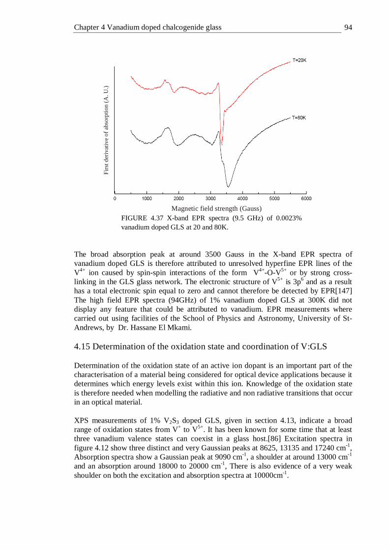
Chapter 4 Vanadium doped chalcogenide glass 94
Magnetic field strength (Gauss)
Fir
st d
eriv
ativ
e of
abs
orpt
ion
(A. U
.)
FIGURE 4.37 X-band EPR spectra (9.5 GHz) of 0.0023% vanadium doped GLS at 20 and 80K.
The broad absorption peak at around 3500 Gauss in the X-band EPR spectra of vanadium doped GLS is therefore attributed to unresolved hyperfine EPR lines of the V4+ ion caused by spin-spin interactions of the form V4+-O-V5+ or by strong cross-linking in the GLS glass network. The electronic structure of V5+ is 3p6 and as a result has a total electronic spin equal to zero and cannot therefore be detected by EPR[147] The high field EPR spectra (94GHz) of 1% vanadium doped GLS at 300K did not display any feature that could be attributed to vanadium. EPR measurements where carried out using facilities of the School of Physics and Astronomy, University of St-Andrews, by Dr. Hassane El Mkami. 4.15 Determination of the oxidation state and coordination of V:GLS Determination of the oxidation state of an active ion dopant is an important part of the characterisation of a material being considered for optical device applications because it determines which energy levels exist within this ion. Knowledge of the oxidation state is therefore needed when modelling the radiative and non radiative transitions that occur in an optical material. XPS measurements of 1% V2S3 doped GLS, given in section 4.13, indicate a broad range of oxidation states from V+ to V5+. It has been known for some time that at least three vanadium valence states can coexist in a glass host.[86] Excitation spectra in figure 4.12 show three distinct and very Gaussian peaks at 8625, 13135 and 17240 cm-1, Absorption spectra show a Gaussian peak at 9090 cm-1, a shoulder at around 13000 cm-1 and an absorption around 18000 to 20000 cm-1, There is also evidence of a very weak shoulder on both the excitation and absorption spectra at 10000cm-1.
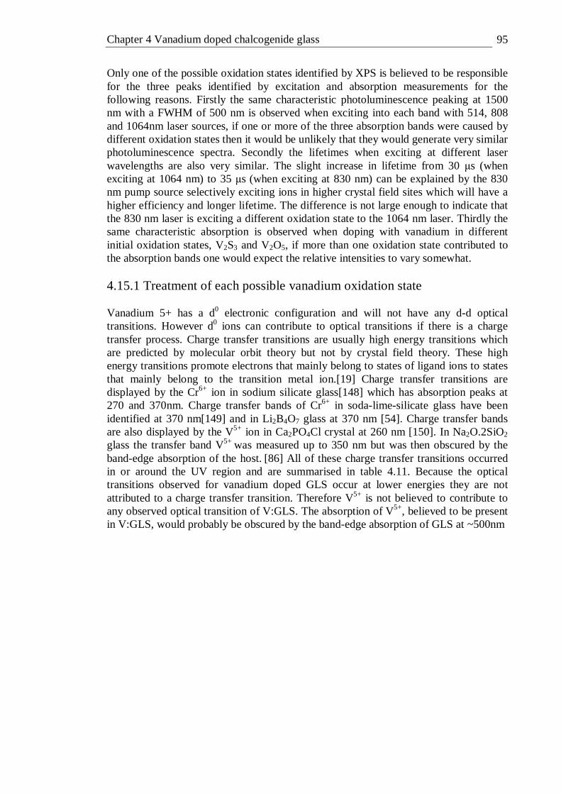
Chapter 4 Vanadium doped chalcogenide glass 95
Only one of the possible oxidation states identified by XPS is believed to be responsible for the three peaks identified by excitation and absorption measurements for the following reasons. Firstly the same characteristic photoluminescence peaking at 1500 nm with a FWHM of 500 nm is observed when exciting into each band with 514, 808 and 1064nm laser sources, if one or more of the three absorption bands were caused by different oxidation states then it would be unlikely that they would generate very similar photoluminescence spectra. Secondly the lifetimes when exciting at different laser wavelengths are also very similar. The slight increase in lifetime from 30 µs (when exciting at 1064 nm) to 35 µs (when exciting at 830 nm) can be explained by the 830 nm pump source selectively exciting ions in higher crystal field sites which will have a higher efficiency and longer lifetime. The difference is not large enough to indicate that the 830 nm laser is exciting a different oxidation state to the 1064 nm laser. Thirdly the same characteristic absorption is observed when doping with vanadium in different initial oxidation states, V2S3 and V2O5, if more than one oxidation state contributed to the absorption bands one would expect the relative intensities to vary somewhat. 4.15.1 Treatment of each possible vanadium oxidation state Vanadium 5+ has a d0 electronic configuration and will not have any d-d optical transitions. However d0 ions can contribute to optical transitions if there is a charge transfer process. Charge transfer transitions are usually high energy transitions which are predicted by molecular orbit theory but not by crystal field theory. These high energy transitions promote electrons that mainly belong to states of ligand ions to states that mainly belong to the transition metal ion.[19] Charge transfer transitions are displayed by the Cr6+ ion in sodium silicate glass[148] which has absorption peaks at 270 and 370nm. Charge transfer bands of Cr6+ in soda-lime-silicate glass have been identified at 370 nm[149] and in Li2B4O7 glass at 370 nm [54]. Charge transfer bands are also displayed by the V5+ ion in Ca2PO4Cl crystal at 260 nm [150]. In Na2O.2SiO2 glass the transfer band V5+ was measured up to 350 nm but was then obscured by the band-edge absorption of the host. [86] All of these charge transfer transitions occurred in or around the UV region and are summarised in table 4.11. Because the optical transitions observed for vanadium doped GLS occur at lower energies they are not attributed to a charge transfer transition. Therefore V5+ is not believed to contribute to any observed optical transition of V:GLS. The absorption of V5+, believed to be present in V:GLS, would probably be obscured by the band-edge absorption of GLS at ~500nm
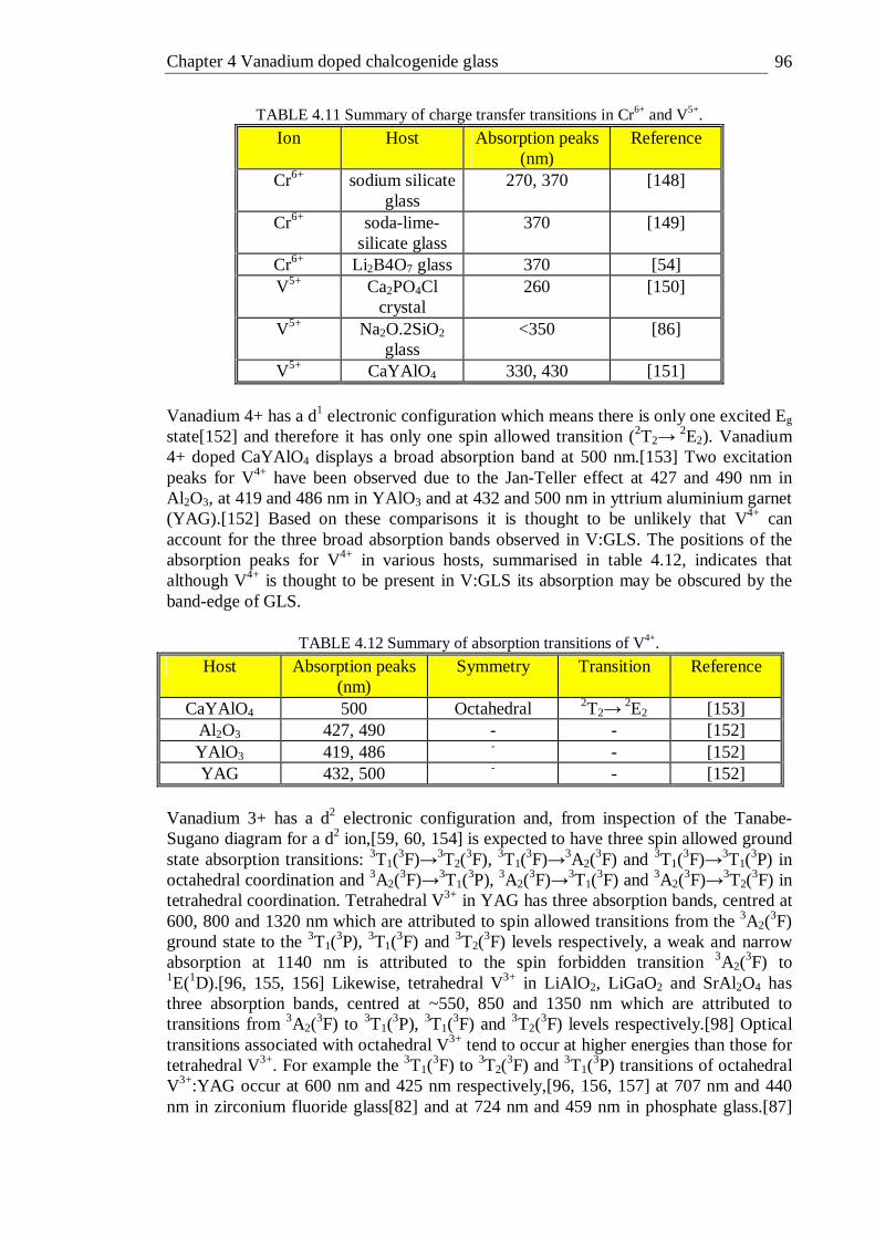
Chapter 4 Vanadium doped chalcogenide glass 96
TABLE 4.11 Summary of charge transfer transitions in Cr6+ and V5+.
Ion Host Absorption peaks (nm)
Reference
Cr6+ sodium silicate glass
270, 370 [148]
Cr6+ soda-lime-silicate glass
370 [149]
Cr6+ Li2B4O7 glass 370 [54]
V5+ Ca2PO4Cl crystal
260 [150]
V5+ Na2O.2SiO2 glass
<350 [86]
V5+ CaYAlO4 330, 430 [151] Vanadium 4+ has a d1 electronic configuration which means there is only one excited Eg state[152] and therefore it has only one spin allowed transition (2T2→ 2E2). Vanadium 4+ doped CaYAlO4 displays a broad absorption band at 500 nm.[153] Two excitation peaks for V4+ have been observed due to the Jan-Teller effect at 427 and 490 nm in Al2O3, at 419 and 486 nm in YAlO3 and at 432 and 500 nm in yttrium aluminium garnet (YAG).[152] Based on these comparisons it is thought to be unlikely that V4+ can account for the three broad absorption bands observed in V:GLS. The positions of the absorption peaks for V4+ in various hosts, summarised in table 4.12, indicates that although V4+ is thought to be present in V:GLS its absorption may be obscured by the band-edge of GLS.
TABLE 4.12 Summary of absorption transitions of V4+.
Host Absorption peaks (nm)
Symmetry Transition Reference
CaYAlO4 500 Octahedral 2T2→ 2E2 [153] Al2O3 427, 490 - - [152] YAlO 3 419, 486 - - [152]
YAG 432, 500 - - [152]
Vanadium 3+ has a d2 electronic configuration and, from inspection of the Tanabe-Sugano diagram for a d2 ion,[59, 60, 154] is expected to have three spin allowed ground state absorption transitions: 3T1(
3F)→3T2(3F), 3T1(
3F)→3A2(3F) and 3T1(
3F)→3T1(3P) in
octahedral coordination and 3A2(3F)→3T1(
3P), 3A2(3F)→3T1(
3F) and 3A2(3F)→3T2(
3F) in tetrahedral coordination. Tetrahedral V3+ in YAG has three absorption bands, centred at 600, 800 and 1320 nm which are attributed to spin allowed transitions from the 3A2(
3F) ground state to the 3T1(
3P), 3T1(3F) and 3T2(
3F) levels respectively, a weak and narrow absorption at 1140 nm is attributed to the spin forbidden transition 3A2(
3F) to 1E(1D).[96, 155, 156] Likewise, tetrahedral V3+ in LiAlO 2, LiGaO2 and SrAl2O4 has three absorption bands, centred at ~550, 850 and 1350 nm which are attributed to transitions from 3A2(
3F) to 3T1(3P), 3T1(
3F) and 3T2(3F) levels respectively.[98] Optical
transitions associated with octahedral V3+ tend to occur at higher energies than those for tetrahedral V3+. For example the 3T1(
3F) to 3T2(3F) and 3T1(
3P) transitions of octahedral V3+:YAG occur at 600 nm and 425 nm respectively,[96, 156, 157] at 707 nm and 440 nm in zirconium fluoride glass[82] and at 724 nm and 459 nm in phosphate glass.[87]
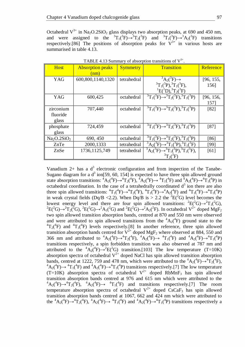
Chapter 4 Vanadium doped chalcogenide glass 97
Octahedral V3+ in Na2O.2SiO2 glass displays two absorption peaks, at 690 and 450 nm, and were assigned to the 3T1(
3F)→3T2(3F) and 3T1(
3F)→3A2(3F) transitions
respectively.[86] The positions of absorption peaks for V3+ in various hosts are summarised in table 4.13.
TABLE 4.13 Summary of absorption transitions of V3+.
Host Absorption peaks (nm)
Symmetry Transition Reference
YAG 600,800,1140,1320 tetrahedral 3A2(3F)→
3T1(3P),3T1(
3F), 1E(1D),3T2(
3F)
[96, 155, 156]
YAG 600,425 octahedral 3T1(3F)→3T2(
3F),3T1(3P) [96, 156,
157] zirconium fluoride
glass
707,440 octahedral 3T1(3F)→3T2(
3F),3T1(3P) [82]
phosphate glass
724,459 octahedral 3T1(3F)→3T2(
3F),3T1(3P) [87]
Na2O.2SiO2 690, 450 octahedral 3T1(3F)→3T2(
3F),3T1(3P) [86]
ZnTe 2000,1333 tetrahedral 3A2(3F)→3T1(
3P),3T1(3F) [99]
ZnSe 1736,1125,749 tetrahedral 3A2(3F)→3T1(
3P),3T1(3F),
3T2(3F)
[61]
Vanadium 2+ has a d3 electronic configuration and from inspection of the Tanabe-Sugano diagram for a d3 ion[59, 60, 154] is expected to have three spin allowed ground state absorption transitions: 4A2(
4F)→4T2(4F), 4A2(
4F)→ 4T1(4F) and 4A2(
4F)→4T1(4P) in
octahedral coordination. In the case of a tetrahedrally coordinated d3 ion there are also three spin allowed transitions: 4T1(
4F)→4T2(4F), 4T1(
4F)→4A2(4F) and 4T1(
4F)→4T1(4P)
in weak crystal fields (Dq/B <2.2). When Dq/B is > 2.2 the 2E(2G) level becomes the lowest energy level and there are four spin allowed transitions: 2E(2G)→2T1(
2G), 2E(2G)→2T2(
2G), 2E(2G)→2A1(2G) and 2E(2G)→2A2(
2F). In octahedral V2+ doped MgF2 two spin allowed transition absorption bands, centred at 870 and 550 nm were observed and were attributed to spin allowed transitions from the 4A2(
4F) ground state to the 4T2(
4F) and 4T1(4F) levels respectively.[8] In another reference, three spin allowed
transition absorption bands centred for V2+ doped MgF2 where observed at 884, 550 and 366 nm and attributed to 4A2(
4F)→4T2(4F), 4A2(
4F)→ 4T1(4F) and 4A2(
4F)→4T1(4P)
transitions respectively, a spin forbidden transition was also observed at 787 nm and attributed to the 4A2(
4F)→2E(2G) transition.[103] The low temperature (T=10K) absorption spectra of octahedral V2+ doped NaCl has spin allowed transition absorption bands, centred at 1222, 759 and 478 nm, which were attributed to the 4A2(
4F)→4T2(4F),
4A2(4F)→ 4T1(
4F) and 4A2(4F)→4T1(
4P) transitions respectively.[7] The low temperature (T=10K) absorption spectra of octahedral V2+ doped RbMnF3 has spin allowed transition absorption bands centred at 976 and 615 nm which were attributed to the 4A2(
4F)→4T2(4F), 4A2(
4F)→ 4T1(4F) and transitions respectively.[7] The room
temperature absorption spectra of octahedral V2+ doped CsCaF3 has spin allowed transition absorption bands centred at 1067, 662 and 424 nm which were attributed to the 4A2(
4F)→4T2(4F), 4A2(
4F)→ 4T1(4F) and 4A2(
4F)→4T1(4P) transitions respectively a
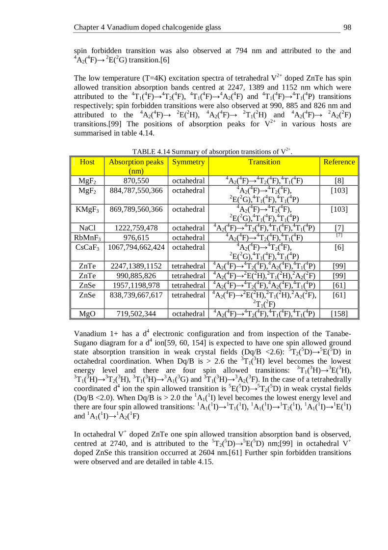
Chapter 4 Vanadium doped chalcogenide glass 98
spin forbidden transition was also observed at 794 nm and attributed to the and 4A2(
4F)→ 2E(2G) transition.[6] The low temperature (T=4K) excitation spectra of tetrahedral V2+ doped ZnTe has spin allowed transition absorption bands centred at 2247, 1389 and 1152 nm which were attributed to the 4T1(
4F)→4T2(4F), 4T1(
4F)→4A2(4F) and 4T1(
4F)→4T1(4P) transitions
respectively; spin forbidden transitions were also observed at 990, 885 and 826 nm and attributed to the 4A2(
4F)→ 2E(2H), 4A2(4F)→ 2T1(
2H) and 4A2(4F)→ 2A2(
2F) transitions.[99] The positions of absorption peaks for V2+ in various hosts are summarised in table 4.14.
TABLE 4.14 Summary of absorption transitions of V2+.
Host Absorption peaks (nm)
Symmetry Transition Reference
MgF2 870,550 octahedral 4A2(4F)→4T2(
4F),4T1(4F) [8]
MgF2 884,787,550,366 octahedral 4A2(4F)→4T2(
4F), 2E(2G),4T1(
4F),4T1(4P)
[103]
KMgF3 869,789,560,366 octahedral 4A2(4F)→4T2(
4F), 2E(2G),4T1(
4F),4T1(4P)
[103]
NaCl 1222,759,478 octahedral 4A2(4F)→4T2(
4F),4T1(4F),4T1(
4P) [7] RbMnF3 976,615 octahedral 4A2(
4F)→4T2(4F),4T1(
4F) [7]
CsCaF3 1067,794,662,424 octahedral 4A2(4F)→4T2(
4F), 2E(2G),4T1(
4F),4T1(4P)
[6]
ZnTe 2247,1389,1152 tetrahedral 4A2(4F)→4T2(
4F),4A2(4F),4T1(
4P) [99] ZnTe 990,885,826 tetrahedral 4A2(
4F)→2E(2H),2T1(2H),2A2(
2F) [99] ZnSe 1957,1198,978 tetrahedral 4A2(
4F)→4T2(4F),4A2(
4F),4T1(4P) [61]
ZnSe 838,739,667,617 tetrahedral 4A2(4F)→2E(2H),2T1(
2H),2A2(2F),
2T1(2F)
[61]
MgO 719,502,344 octahedral 4A2(4F)→4T2(
4F),4T1(4F),4T1(
4P) [158] Vanadium 1+ has a d4 electronic configuration and from inspection of the Tanabe-Sugano diagram for a d4 ion[59, 60, 154] is expected to have one spin allowed ground state absorption transition in weak crystal fields (Dq/B <2.6): 5T2(
5D)→5E(5D) in octahedral coordination. When Dq/B is > 2.6 the 3T1(
3H) level becomes the lowest energy level and there are four spin allowed transitions: 3T1(
3H)→3E(3H), 3T1(
3H)→3T2(3H), 3T1(
3H)→3A1(3G) and 3T1(
3H)→3A2(3F). In the case of a tetrahedrally
coordinated d4 ion the spin allowed transition is 5E(5D)→5T2(5D) in weak crystal fields
(Dq/B <2.0). When Dq/B is > 2.0 the 1A1(1I) level becomes the lowest energy level and
there are four spin allowed transitions: 1A1(1I)→1T1(
1I), 1A1(1I)→1T2(
1I), 1A1(1I)→1E(1I)
and 1A1(1I)→1A2(
1F) In octahedral V+ doped ZnTe one spin allowed transition absorption band is observed, centred at 2740, and is attributed to the 5T2(
5D)→5E(5D) nm;[99] in octahedral V+ doped ZnSe this transition occurred at 2604 nm.[61] Further spin forbidden transitions were observed and are detailed in table 4.15.
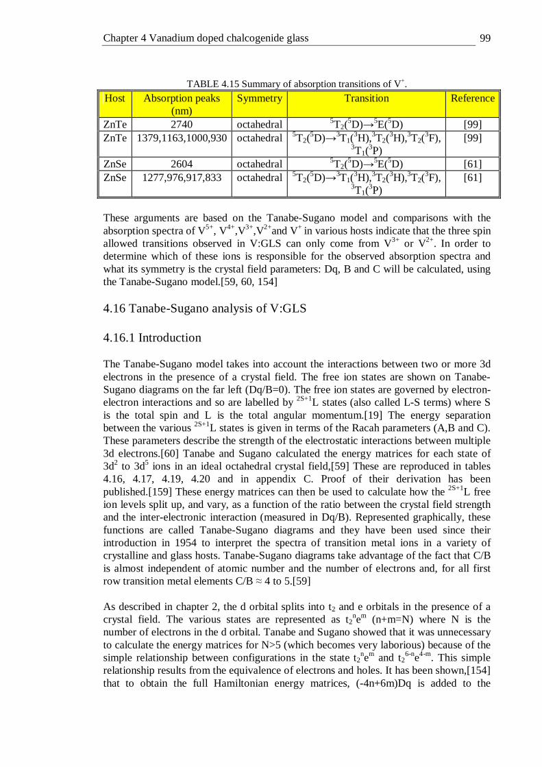
Chapter 4 Vanadium doped chalcogenide glass 99
TABLE 4.15 Summary of absorption transitions of V+.
Host Absorption peaks (nm)
Symmetry Transition Reference
ZnTe 2740 octahedral 5T2(5D)→5E(5D) [99]
ZnTe 1379,1163,1000,930 octahedral 5T2(5D)→3T1(
3H),3T2(3H),3T2(
3F), 3T1(
3P) [99]
ZnSe 2604 octahedral 5T2(5D)→5E(5D) [61]
ZnSe 1277,976,917,833 octahedral 5T2(5D)→3T1(
3H),3T2(3H),3T2(
3F), 3T1(
3P) [61]
These arguments are based on the Tanabe-Sugano model and comparisons with the absorption spectra of V5+, V4+,V3+,V2+and V+ in various hosts indicate that the three spin allowed transitions observed in V:GLS can only come from V3+ or V2+. In order to determine which of these ions is responsible for the observed absorption spectra and what its symmetry is the crystal field parameters: Dq, B and C will be calculated, using the Tanabe-Sugano model.[59, 60, 154] 4.16 Tanabe-Sugano analysis of V:GLS 4.16.1 Introduction The Tanabe-Sugano model takes into account the interactions between two or more 3d electrons in the presence of a crystal field. The free ion states are shown on Tanabe-Sugano diagrams on the far left (Dq/B=0). The free ion states are governed by electron-electron interactions and so are labelled by 2S+1L states (also called L-S terms) where S is the total spin and L is the total angular momentum.[19] The energy separation between the various 2S+1L states is given in terms of the Racah parameters (A,B and C). These parameters describe the strength of the electrostatic interactions between multiple 3d electrons.[60] Tanabe and Sugano calculated the energy matrices for each state of 3d2 to 3d5 ions in an ideal octahedral crystal field,[59] These are reproduced in tables 4.16, 4.17, 4.19, 4.20 and in appendix C. Proof of their derivation has been published.[159] These energy matrices can then be used to calculate how the 2S+1L free ion levels split up, and vary, as a function of the ratio between the crystal field strength and the inter-electronic interaction (measured in Dq/B). Represented graphically, these functions are called Tanabe-Sugano diagrams and they have been used since their introduction in 1954 to interpret the spectra of transition metal ions in a variety of crystalline and glass hosts. Tanabe-Sugano diagrams take advantage of the fact that C/B is almost independent of atomic number and the number of electrons and, for all first row transition metal elements C/B ≈ 4 to 5.[59] As described in chapter 2, the d orbital splits into t2 and e orbitals in the presence of a crystal field. The various states are represented as t2
nem (n+m=N) where N is the number of electrons in the d orbital. Tanabe and Sugano showed that it was unnecessary to calculate the energy matrices for N>5 (which becomes very laborious) because of the simple relationship between configurations in the state t2
nem and t26-ne4-m. This simple
relationship results from the equivalence of electrons and holes. It has been shown,[154] that to obtain the full Hamiltonian energy matrices, (-4n+6m)Dq is added to the
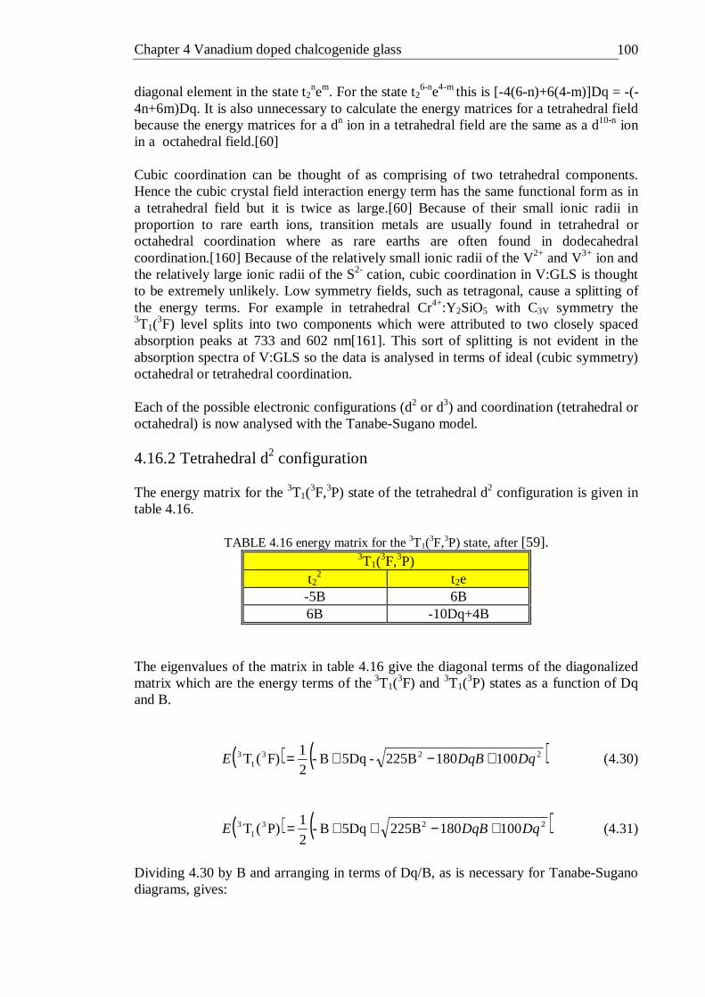
Chapter 4 Vanadium doped chalcogenide glass 100
diagonal element in the state t2nem. For the state t2
6-ne4-m this is [-4(6-n)+6(4-m)]Dq = -(-4n+6m)Dq. It is also unnecessary to calculate the energy matrices for a tetrahedral field because the energy matrices for a dn ion in a tetrahedral field are the same as a d10-n ion in a octahedral field.[60] Cubic coordination can be thought of as comprising of two tetrahedral components. Hence the cubic crystal field interaction energy term has the same functional form as in a tetrahedral field but it is twice as large.[60] Because of their small ionic radii in proportion to rare earth ions, transition metals are usually found in tetrahedral or octahedral coordination where as rare earths are often found in dodecahedral coordination.[160] Because of the relatively small ionic radii of the V2+ and V3+ ion and the relatively large ionic radii of the S2- cation, cubic coordination in V:GLS is thought to be extremely unlikely. Low symmetry fields, such as tetragonal, cause a splitting of the energy terms. For example in tetrahedral Cr4+:Y2SiO5 with C3V symmetry the 3T1(
3F) level splits into two components which were attributed to two closely spaced absorption peaks at 733 and 602 nm[161]. This sort of splitting is not evident in the absorption spectra of V:GLS so the data is analysed in terms of ideal (cubic symmetry) octahedral or tetrahedral coordination. Each of the possible electronic configurations (d2 or d3) and coordination (tetrahedral or octahedral) is now analysed with the Tanabe-Sugano model. 4.16.2 Tetrahedral d2 configuration The energy matrix for the 3T1(
3F,3P) state of the tetrahedral d2 configuration is given in table 4.16.
TABLE 4.16 energy matrix for the 3T1(3F,3P) state, after [59].
3T1(3F,3P)
t22 t2e
-5B 6B 6B -10Dq+4B
The eigenvalues of the matrix in table 4.16 give the diagonal terms of the diagonalized matrix which are the energy terms of the 3T1(
3F) and 3T1(3P) states as a function of Dq
and B.
( ) ( )2231
3 100180225B-5DqB-2
1 F)(T DqDqBE +−+= (4.30)
( ) ( )2231
3 100180225B5DqB-2
1 P)(T DqDqBE +−++= (4.31)
Dividing 4.30 by B and arranging in terms of Dq/B, as is necessary for Tanabe-Sugano diagrams, gives:

Chapter 4 Vanadium doped chalcogenide glass 101
( ) 231
3 )/(100/1802252
1-5Dq/B
2
1 /BF)(T BDqBDqE +−+−= (4.32)
Note that 4.32 is independent of C, in order to calculate C the energy term for a spin forbidden transition is needed. Table 4.17 gives the energy matrix for the 1E(1D,1G) state.
Table 4.17 energy matrix for the 1E(1D,1G) state, after [59].
1E(1D,1G) t2
2 e2
B+2C -2√3B -2√3B -20Dq+2C
Diagonalising and dividing by B gives:
( ) 211 )/(400/40492
110Dq/B/2
2
1 /BG)E( BDqBDqBCE +++−+= (4.33)
and
( ) 211 )/(400/40492
110Dq/B/2
2
1 /BD)E( BDqBDqBCE ++−−+= (4.34)
Figure 4.38 shows the energy terms of a tetrahedral d2 ion, plotted as a function of Dq/B, note that the lowest energy level is less than zero and varies as a function of Dq/B. The energy matrices and energy terms for all the energy levels are given in appendix C.
Dq/B
0 1 2 3 4
E/B
-100
-80
-60
-40
-20
0
20
40
3T1(3F)
3T2(3F)
3A2(3F)
1T2(1D)
1E(1D) 3T1(
3P) 1T2(
1G) 1E(1G) 1T1(
1G) 1A1(
1G)
FIGURE 4.38 Energy terms of a tetrahedral d2 ion plotted as a function of Dq/B.
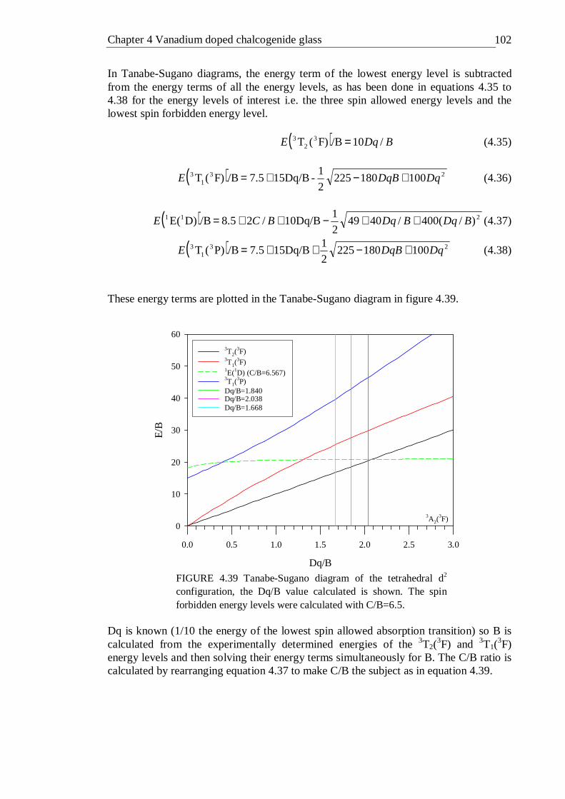
Chapter 4 Vanadium doped chalcogenide glass 102
In Tanabe-Sugano diagrams, the energy term of the lowest energy level is subtracted from the energy terms of all the energy levels, as has been done in equations 4.35 to 4.38 for the energy levels of interest i.e. the three spin allowed energy levels and the lowest spin forbidden energy level.
( ) BDqE /10 /BF)(T 32
3 = (4.35)
( ) 231
3 1001802252
1-5Dq/B17.5 /BF)(T DqDqBE +−+= (4.36)
( ) 211 )/(400/40492
110Dq/B/25.8 /BD)E( BDqBDqBCE ++−++= (4.37)
( ) 231
3 1001802252
15Dq/B17.5 /BP)(T DqDqBE +−++= (4.38)
These energy terms are plotted in the Tanabe-Sugano diagram in figure 4.39.
Dq/B
0.0 0.5 1.0 1.5 2.0 2.5 3.0
E/B
0
10
20
30
40
50
60
3T2(3F)
3T1(3F)
1E(1D) (C/B=6.567) 3T1(
3P) Dq/B=1.840 Dq/B=2.038 Dq/B=1.668
3A2(3F)
FIGURE 4.39 Tanabe-Sugano diagram of the tetrahedral d2 configuration, the Dq/B value calculated is shown. The spin forbidden energy levels were calculated with C/B=6.5.
Dq is known (1/10 the energy of the lowest spin allowed absorption transition) so B is calculated from the experimentally determined energies of the 3T2(
3F) and 3T1(3F)
energy levels and then solving their energy terms simultaneously for B. The C/B ratio is calculated by rearranging equation 4.37 to make C/B the subject as in equation 4.39.
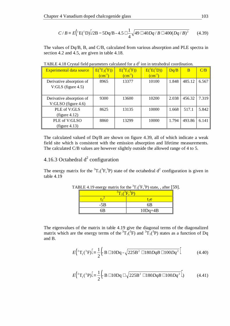
Chapter 4 Vanadium doped chalcogenide glass 103
( ) 211 )/(400/40494
14.5-5Dq/B /2BD)E( / BDqBDqEBC +++−= (4.39)
The values of Dq/B, B, and C/B, calculated from various absorption and PLE spectra in section 4.2 and 4.5, are given in table 4.18. TABLE 4.18 Crystal field parameters calculated for a d2 ion in tetrahedral coordination.
Experimental data source E(3T2(3F))
(cm-1) E(3T1(
3F)) (cm-1)
E(1E(1D)) (cm-1)
Dq/B B C/B
Derivative absorption of V:GLS (figure 4.5)
8965 13377 10100 1.848 485.12 6.567
Derivative absorption of V:GLSO (figure 4.6)
9300 13600 10200 2.038 456.32 7.319
PLE of V:GLS (figure 4.12)
8625 13135 10000 1.668 517.1 5.842
PLE of V:GLSO (figure 4.13)
8860 13299 10000 1.794 493.86 6.141
The calculated valued of Dq/B are shown on figure 4.39, all of which indicate a weak field site which is consistent with the emission absorption and lifetime measurements. The calculated C/B values are however slightly outside the allowed range of 4 to 5. 4.16.3 Octahedral d2 configuration The energy matrix for the 3T1(
3F,3P) state of the octahedral d2 configuration is given in table 4.19
TABLE 4.19 energy matrix for the 3T1(3F,3P) state, , after [59].
3T1(3F,3P)
t22 t2e
-5B 6B 6B 10Dq+4B
The eigenvalues of the matrix in table 4.19 give the diagonal terms of the diagonalized matrix which are the energy terms of the 3T1(
3F) and 3T1(3P) states as a function of Dq
and B.
( ) ( )2231
3 100180225B-10DqB-2
1 F)(T DqDqBE +++= (4.40)
( ) ( )2231
3 100180225B10DqB-2
1 P)(T DqDqBE ++++= ) (4.41)

Chapter 4 Vanadium doped chalcogenide glass 104
Dividing equation 4.40 by B and arranging it in terms of Dq/B, as is necessary for Tanabe-Sugano diagrams, gives:
( ) 231
3 )/(100/1802252
1-5Dq/B
2
1 /BF)(T BDqBDqE +++−= (4.42)
Note that equation 4.42 is independent of C, in order to calculate C the energy term for a spin forbidden transition is needed. Table 4.20 gives the energy matrix for the 1E(1D,1G) state.
TABLE 4.20 energy matrix for the 1E(1D,1G) state, , after [59]. 1E(1D,1G)
t22 e2
B+2C -2√3B -2√3B 20Dq+2C
Diagonalising and dividing by B gives:
( ) 211 )/(400/40492
1-10Dq/B/2
2
1 /BD)E( BDqBDqBCE +−++= (4.43)
and
( ) 211 )/(400/40492
110Dq/B/2
2
1 /BG)E( BDqBDqBCE +−+++= (4.44)
Similarly, for the case of a d2 tetrahedral ion, the energy terms of interest are given in equation 4.45 to 4.49 and plotted in the Tanabe-Sugano diagram in figure 4.40. The values of Dq/B, B and C/B were calculated using the same method as described for a d2 tetrahedral ion. The energy term for the 1E(1D) level was used to calculate C/B, as shown in figure 4.40 this energy level is virtually indistinguishable from the 1T2(
1D) level.
( ) 232
3 )/(100/1802252
15Dq/B
2
17 /BF)(T BDqBDqE ++++−= (4.45)
( ) 232
3 )/(100/1802252
15Dq/B1
2
17 /BF)(A BDqBDqE ++++−= (4.46)
( )2
211
)/(100/1802252
1
)/(400/40492
1-5Dq/B/21 /BD)E(
BDqBDq
BDqBDqBCE
+++
+−++= (4.47)
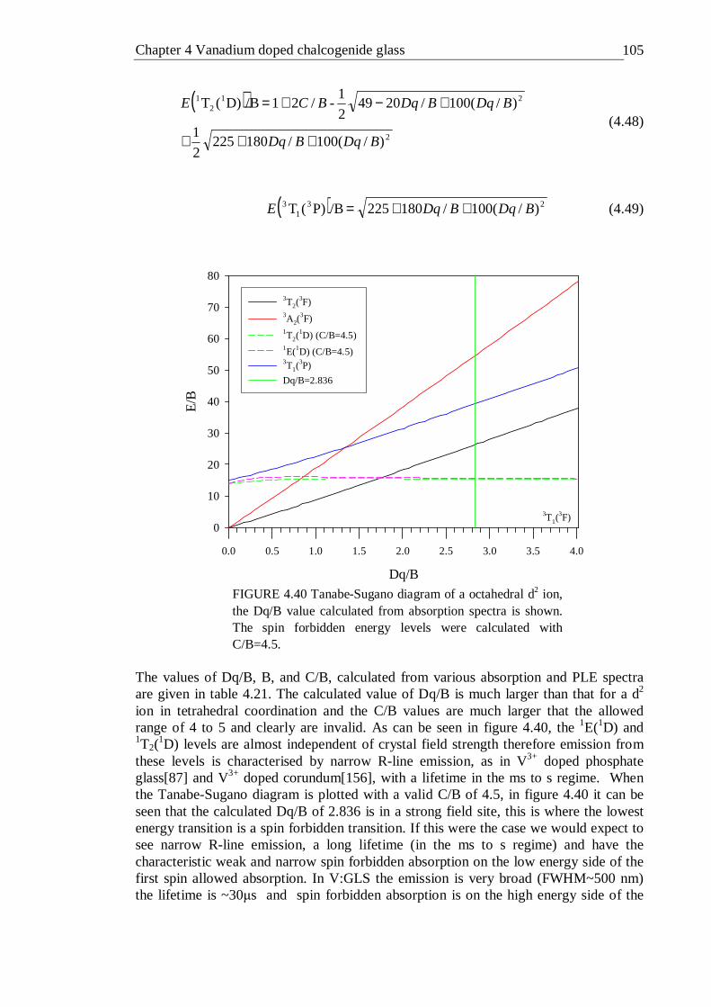
Chapter 4 Vanadium doped chalcogenide glass 105
( )2
212
1
)/(100/1802252
1
)/(100/20492
1-/21 /BD)(T
BDqBDq
BDqBDqBCE
+++
+−+= (4.48)
( ) 231
3 )/(100/180225 /BP)(T BDqBDqE ++= (4.49)
Dq/B
0.0 0.5 1.0 1.5 2.0 2.5 3.0 3.5 4.0
E/B
0
10
20
30
40
50
60
70
80
3T2(3F)
3A2(3F)
1T2(1D) (C/B=4.5)
1E(1D) (C/B=4.5)3T1(
3P)
Dq/B=2.836
3T1(3F)
FIGURE 4.40 Tanabe-Sugano diagram of a octahedral d2 ion, the Dq/B value calculated from absorption spectra is shown. The spin forbidden energy levels were calculated with C/B=4.5.
The values of Dq/B, B, and C/B, calculated from various absorption and PLE spectra are given in table 4.21. The calculated value of Dq/B is much larger than that for a d2 ion in tetrahedral coordination and the C/B values are much larger that the allowed range of 4 to 5 and clearly are invalid. As can be seen in figure 4.40, the 1E(1D) and 1T2(
1D) levels are almost independent of crystal field strength therefore emission from these levels is characterised by narrow R-line emission, as in V3+ doped phosphate glass[87] and V3+ doped corundum[156], with a lifetime in the ms to s regime. When the Tanabe-Sugano diagram is plotted with a valid C/B of 4.5, in figure 4.40 it can be seen that the calculated Dq/B of 2.836 is in a strong field site, this is where the lowest energy transition is a spin forbidden transition. If this were the case we would expect to see narrow R-line emission, a long lifetime (in the ms to s regime) and have the characteristic weak and narrow spin forbidden absorption on the low energy side of the first spin allowed absorption. In V:GLS the emission is very broad (FWHM~500 nm) the lifetime is ~30µs and spin forbidden absorption is on the high energy side of the
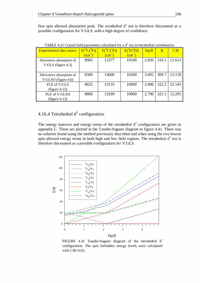
Chapter 4 Vanadium doped chalcogenide glass 106
first spin allowed absorption peak. The octahedral d2 ion is therefore discounted as a possible configuration for V:GLS, with a high degree of confidence.
TABLE 4.21 Crystal field parameters calculated for a d2 ion in tetrahedral coordination.
Experimental data source E(3T2(3F))
(cm-1) E(3T1(
3P)) (cm-1)
E(1E(1D)) (cm-1)
Dq/B B C/B
Derivative absorption of V:GLS (figure 4.5)
8965 13377 10100 2.836 316.1 12.613
Derivative absorption of V:GLSO (figure 4.6)
9300 13600 10200 3.002 309.7 13.118
PLE of V:GLS (figure 4.12)
8625 13135 10000 2.686 322.2 12.143
PLE of V:GLSO (figure 4.13)
8860 13299 10000 2.790 321.1 12.205
4.16.4 Tetrahedral d3 configuration The energy matrices and energy terms of the tetrahedral d3 configuration are given in appendix C. These are plotted in the Tanabe-Sugano diagram in figure 4.41. There was no solution found using the method previously described and when using the two lowest spin allowed energy terms in both high and low field regions. The tetrahedral d3 ion is therefore discounted as a possible configuration for V:GLS.
Dq/B
0 1 2 3 4
E/B
0
20
40
60
80
100
120
4T1g(4F)
4T2g(4F)
4A2g(4F)
4T1g(4P)
2T2g(2G)
2Eg(2G)
2T1g(2G)
2A1g(2G)
FIGURE 4.41 Tanabe-Sugano diagram of the tetrahedral d3 configuration. The spin forbidden energy levels were calculated with C/B=4.63.
Chapter 4 Vanadium doped chalcogenide glass 107
4.16.5 Octahedral d3 configuration The energy terms of interest for the octahedral d3 configuration are given in equations 4.50 to 4.54
( ) BDqE /10 /BF)(T 42
4 = (4.50)
( ) 241
4 1001802252
1-5Dq/B17.5 /BF)(T DqDqBE +−+= (4.51)
( ) 241
4 1001802252
15Dq/B17.5 /BP)(T DqDqBE +−++= (4.52)
( ) ( )( ) 15120det1)(22
−−=−=B
DqIMroot
B
GEE st λ (4.53)
where
++−+
−+−−
+−+−
−−−+−
=
B
Dq
B
C
B
CB
Dq
B
CB
C
B
Dq
B
CB
Dq
B
C
M
184832)2(30
322311023
)2(31026826
023261236
( ) ( )( ) 15120det1)(2
12
−−=−=B
DqIMroot
B
GTE st λ (4.54)
where
++−−−
++−−
−−−+−−
−−−
−−−−−
=
B
Dq
B
CB
Dq
B
CB
Dq
B
CB
Dq
B
CB
Dq
B
C
M
8323233332
32836330
3323633
3333233
320331236
The energy terms for the 2E(2G) and 2T2(
2G) levels cannot be easily expressed explicitly, therefore they are defined in terms of the solution to the characteristic equation of the energy matrix of the 2E state, in which each matrix element has been

Chapter 4 Vanadium doped chalcogenide glass 108
divided by B to give the equation in terms of E/B. Where I is the identity matrix and the first root is the numerically smallest root in the zero crystal field (Dq=0) case. Comparing these equations to those for the tetrahedral d2 configuration it can be seen that the energy terms for the three spin allowed energy levels are exactly the same for both configurations. The only difference between the energy terms of interest are for the spin forbidden energy levels. This now presents a problem for determining which of these configurations is most representative of V:GLS since only analysis of the spin forbidden terms can achieve this. The C/B ratio for this configuration was calculated from the energy term for the 2E(2G) multiplied by B to give it in terms of E(2E(2G)). The values of Dq and E(2E(2G)) were defined from experimentally determined values, B was calculated by solving equations 4.50 and 4.51 simultaneously for B. Then C was calculated by solving this equation for C. Because of the equations’ complexity the equation solving facility of Mathematica software was used. As can been seen in the Tanabe-Sugano diagram for this configuration in figure 4.42 the 2T2(
2G) level lies close to the 2E(2G) level so the spin forbidden transition could be caused by a transition to either or both of these energy levels. Because of this, C/B was also calculated using the energy term for the 2T2(
2G) energy level. The values of Dq/B, B and the energy of the 4T1(
4P) level that was predicted by the Tanabe-Sugano model, calculated from various absorption and PLE spectra, are given in table 4.22. TABLE 4.22 Dq and B crystal field parameters calculated for the octahedral d3 configuration. The energy of the 4T1(
4P) level was calculated from the Tanabe-Sugano model.
Experimental data source
E(4T2(4F))
(cm-1) E(4T1(
4F)) (cm-1)
E(2E(2G)) (cm-1)
E(4T1(4P))
(cm-1) Dq/B B
Derivative absorption of
V:GLS (figure 4.5)
8965 13377 10100 20795 1.848 485.1
Derivative absorption of
V:GLSO (figure 4.6)
9300 13600 10200 21146 2.038 456.3
PLE of V:GLS (figure 4.12)
8625 13135 10000 20499 1.668 517.1
PLE of V:GLSO (figure 4.13)
8860 13299 10000 20689 1.7940 493.9
Table 4.22 gives the energy of the 4T1(
4P) level that was calculated from its energy term equation 4.52. These are 20795 cm-1(481 nm) from the absorption measurements of V:GLS, which is consistent with estimates of the centre of gravity for this absorption band in section 4.1 of ~500 nm. It was also noted that this estimate may be at a longer wavelength than the true centre of gravity for this absorption band because it was so heavily obscured by the band-edge absorption of GLS. The steeper gradient of the 4T1(
4P) level, in comparison the 4T2(4F) and 4T1(
4F) levels is consistent with the greater bandwidth of the 4T1(
4P) level observed in the PLE spectra of V:GLS (figure 4.12). For V:GLSO the calculated energy of the 4T1(
4P) level is 21146 cm-1(472 nm), the higher energy of this transition than for V:GLS is consistent with the higher energy of the experimentally determined transitions in V:GLSO. For the PLE measurements the lower
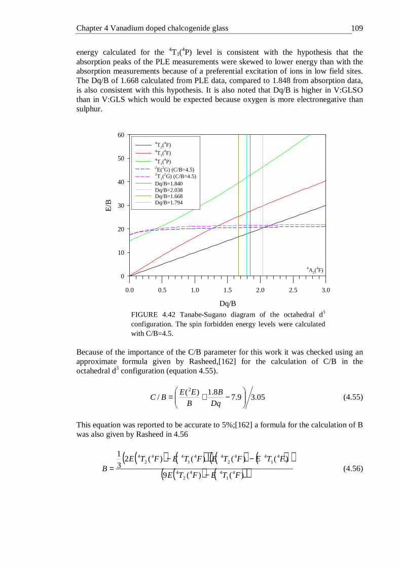
Chapter 4 Vanadium doped chalcogenide glass 109
energy calculated for the 4T1(4P) level is consistent with the hypothesis that the
absorption peaks of the PLE measurements were skewed to lower energy than with the absorption measurements because of a preferential excitation of ions in low field sites. The Dq/B of 1.668 calculated from PLE data, compared to 1.848 from absorption data, is also consistent with this hypothesis. It is also noted that Dq/B is higher in V:GLSO than in V:GLS which would be expected because oxygen is more electronegative than sulphur.
Dq/B
0.0 0.5 1.0 1.5 2.0 2.5 3.0
E/B
0
10
20
30
40
50
604T2(
4F) 4T1(
4F) 4T1(
4P) 2E(2G) (C/B=4.5)2T1(
2G) (C/B=4.5)Dq/B=1.840 Dq/B=2.038 Dq/B=1.668 Dq/B=1.794
4A2(4F)
FIGURE 4.42 Tanabe-Sugano diagram of the octahedral d3 configuration. The spin forbidden energy levels were calculated with C/B=4.5.
Because of the importance of the C/B parameter for this work it was checked using an approximate formula given by Rasheed,[162] for the calculation of C/B in the octahedral d3 configuration (equation 4.55).
05.39.78.1)(
/2
−+=
Dq
B
B
EEBC (4.55)
This equation was reported to be accurate to 5%;[162] a formula for the calculation of B was also given by Rasheed in 4.56
( ) ( )( ) ( ) ( )( )( ) ( )( ))()(9
)()()()(23
1
41
442
4
41
442
441
442
4
FTEFTE
FTEFTEFTEFTEB
−
−−= (4.56)

Chapter 4 Vanadium doped chalcogenide glass 110
TABLE 4.23 B and C/B crystal field parameters calculated for the octahedral d3 configuration. Experimental data
source B B
(equation 4.56) C/B
(2E(2G)) C/B
(2T1(2G))
C/B (equation 4.55)
Derivative absorption of
V:GLS (figure 4.5) 485.12 485.21 4.553 4.247 4.554
Derivative absorption of V:GLSO (figure 4.6)
456.32 456.48 4.934 4.7367 5.025
PLE of V:GLS (figure 4.12)
517.09 517.67 4.164 3.777 4.097
PLE of V:GLSO (figure 4.13)
493.87 493.89 4.403 4.063 4.377
Table 4.23 gives the values of B calculated by solving the energy terms of the two lowest energy levels simultaneously for B and by using equation 4.56. Table 4.23 also gives C/B calculated from the energy term for the 2E(2G) and 2T2(
2G) energy levels and from equation 4.55. The values of B, calculated using the method detailed in this work and by equation 4.56 are almost identical. Calculation of B using equation 4.56 is the simplest method however this equation does not apply to all the configurations dealt with in this study. The values of C/B calculated using the energy term for the 2E(2G) energy level are all in the allowed range of 4 to 5 unlike those calculated for the tetrahedral d2 configuration which were 5.8 to 6.6. The calculated values of Dq/B are shown in the Tanabe-Sugano diagram in figure 4.42 and all indicate a weak field site which is consistent with the emission absorption and lifetime measurements. For the Dq/B of 2.038 the C/B value is higher than that used to plot figure 4.42 while it appears in the figure to be at the cross over point of the spin forbidden and spin allowed transition, when plotted with the correct C/B it is in a weak field site. In tetrahedral d2 configuration the 3A2(
3F)→ 3T2(3F) transition is expected to be significantly weaker than
the other two spin allowed transitions because it is only magnetic dipole allowed,[163, 164] however this is not evident from the derivative absorption and PLE spectra of V:GLS in figure 4.5 and 4.12, this indicates that V:GLS, may not have a tetrahedral d2 configuration. The above arguments indicate that the octahedral d3 configuration is more representative of V:GLS than the tetrahedral d2 configuration. One of the values of C/B calculated using the energy term for the 2T2(
2G ) energy level is just outside the allowed range which indicates that the spin forbidden transition is more likely to be due to a transition to the 2E(2G) energy level. The C/B value calculated using equation 4.55 appears to be a good approximation to the method described in this work and it is much simpler to calculate. This indicated that equation 4.55 would be a more suitable method for calculating C/B when maximum precision is not required. It is therefore proposed that the three spin allowed absorption bands identified in figure 4.12 at 1160, 760 and 580 nm are due to 4A2(
4F)→ 4T2(4F), 4A2(
4F)→ 4T1(4F) and
4A2(4F)→ 4T1(
4P) transitions respectively and the spin forbidden transition at 1000 nm identified in figure 4.5 is attributed to the 4A2(
4F)→ 2E(2G). From the bandwidths of these absorption bands, calculated in figure 4.12, the energy level diagram for vanadium doped GLS is given in figure 4.43.

Chapter 4 Vanadium doped chalcogenide glass 111
Ene
rgy
(cm-1
)
0
5000
10000
15000
20000
4T2(4F)
2E(2G)
4T1(4F)
4T1(4P)
FIGURE 4.43 Energy level diagram of vanadium 2+ doped GLS
4.18 Conclusions V:GLS was optically characterised to investigate its suitability as an active material for an optical device. Absorption measurements of V:GLS unambiguously identified one absorption band at 1100 nm, with evidence of a spin forbidden transition around 1000 nm, and two further higher energy absorption bands that could not be resolved. Derivative analysis of the absorption measurements clarified the identification of the spin forbidden transition and was able to resolve the second highest, but not the highest, energy absorption band at 750 nm. PLE measurements were able to resolve all three absorption bands, peaking at 1160, 760 and 580 nm. However there was a preferential detection of ions in low crystal field strength sites. XPS measurements indicated the presence of vanadium in a broad range of oxidation states from V+ to V5+. Excitation into each of the three absorption bands produced the same characteristic emission spectrum, peaking at 1500 nm with a FWHM of ~500nm. The decay lifetime and decay profile were also similar. This was a strong indication that only one of the vanadium oxidation states was responsible for the observed absorption bands. The quantum efficiency of 0.0023 % V:GLS was 4.2 %. Out of the possible vanadium oxidation states, only V2+ and V3+ is expected to exhibit three spin allowed transitions. Tanabe-Sugano analysis indicates that out of the possible configurations of coordination and oxidation state only tetrahedral V3+ and octahedral V2+ had a crystal field strength in the expected low field region. Out of these configurations only octahedral V2+ had a C/B value in the expected range of 4-5. The configuration of the optically active vanadium ion in V:GLS is therefore proposed to be octahedral V2+. The crystal field strengths (Dq/B) calculated from absorption measurements of V:GLS and V:GLSO are 1.84 and 2.04 respectively.
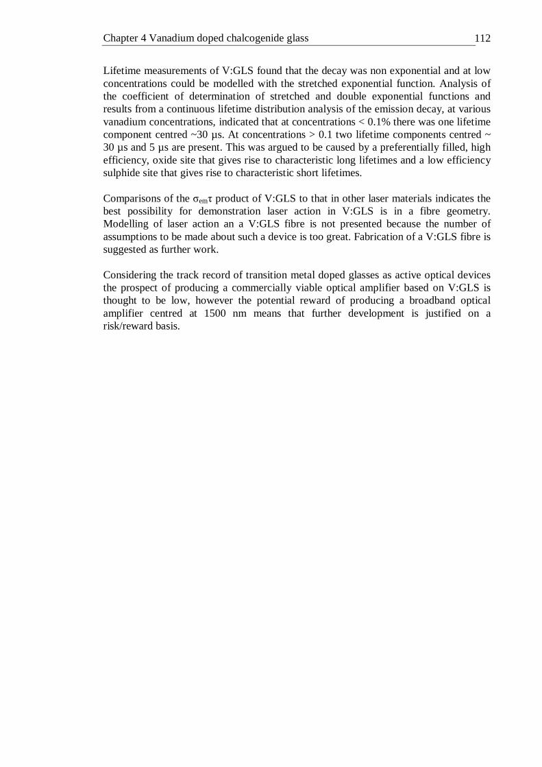
Chapter 4 Vanadium doped chalcogenide glass 112
Lifetime measurements of V:GLS found that the decay was non exponential and at low concentrations could be modelled with the stretched exponential function. Analysis of the coefficient of determination of stretched and double exponential functions and results from a continuous lifetime distribution analysis of the emission decay, at various vanadium concentrations, indicated that at concentrations < 0.1% there was one lifetime component centred ~30 µs. At concentrations > 0.1 two lifetime components centred ~ 30 µs and 5 µs are present. This was argued to be caused by a preferentially filled, high efficiency, oxide site that gives rise to characteristic long lifetimes and a low efficiency sulphide site that gives rise to characteristic short lifetimes. Comparisons of the σemτ product of V:GLS to that in other laser materials indicates the best possibility for demonstration laser action in V:GLS is in a fibre geometry. Modelling of laser action an a V:GLS fibre is not presented because the number of assumptions to be made about such a device is too great. Fabrication of a V:GLS fibre is suggested as further work. Considering the track record of transition metal doped glasses as active optical devices the prospect of producing a commercially viable optical amplifier based on V:GLS is thought to be low, however the potential reward of producing a broadband optical amplifier centred at 1500 nm means that further development is justified on a risk/reward basis.

Chapter 5 Titanium, nickel and bismuth doped chalcogenide glass 113
Chapter 5
Titanium, nickel and bismuth doped chalcogenide glass 5.1 Introduction This chapter details the spectroscopic properties of titanium, nickel and bismuth doped GLS which, like vanadium doped GLS detailed in chapter 4, may have applications as active optical devices because they display strong infrared emission. Prior studies have been conducted on this topic but there are still some areas to investigate. It was found that the emission of Ti, Ni and Bi:GLS peaks at ~900 nm, which is less useful for telecommunication applications compared to the emission of V:GLS which peaked ~1500 nm. Reports of emission from Ti and Ni doped glasses are scarce in the literature. However, there are many reports of emission from Bi doped glasses[165-174] and laser action been demonstrated in a bismuth doped aluminosilicate fibre laser.[84] Iron, cobalt and copper doped GLS were also investigated by the author however no emission in the range 800-1800 nm could be detected from these dopants so they are not included in this report. Chromium doped GLS was also studied, however this has been previously investigated in detail by Aronson.[23] The absorption of titanium, nickel, iron and cobalt doped GLS has been reported by Aronson[23] and Brady.[70] Petrovich[24] reported the absorption of nickel, iron and cobalt doped GLS. Aronson reported emission from Ni:GLS when exciting at 800 nm, which is at the long wavelength end of the Ni:GLS excitation range. Aronson did not attribute an oxidation state to Ti:GLS whereas Brady speculated it was in a 4+ oxidation state. Aronson, Brady and Petrovich all proposed Ni:GLS was in a 2+ oxidation state; in this chapter evidence is provided that Ni:GLS is in a 1+ oxidation. This is the first time the optical properties of bismuth doped GLS have been reported. Glasses were melted using the method detailed in section 3.2.1. 5.2 Titanium doped GLS Titanium doped Al2O3 (Ti:Sapphire) has been used as a gain medium in room temperature tuneable lasers since laser action was first reported by Moulton in 1982.[4] The Ti:Sapphire laser is the most widely used near infrared tuneable laser source and is tuneable from 650 to 1100 nm, it is also used to generate ultra short laser pulses with durations as low as 8 fs.[80] Because of the success of the Ti:Sapphire crystal as a tuneable laser source little attention has been paid to titanium doped glass as an active medium and reports in the literature of photoluminescence from titanium doped glasses are extremely scarce. A titanium doped glass laser in a fibre geometry could potentially have several advantages over a Ti:Sapphire laser in that it could be more compact, have a higher alignment stability and robustness.
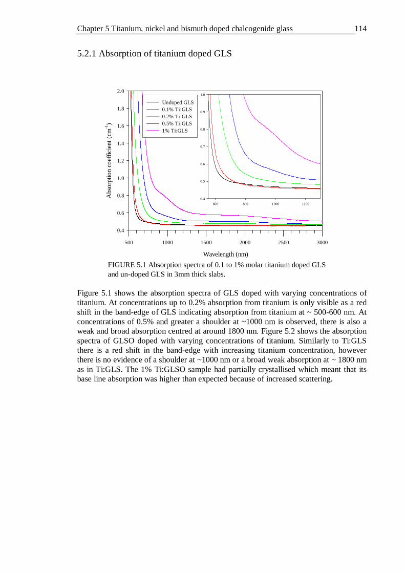
Chapter 5 Titanium, nickel and bismuth doped chalcogenide glass 114
5.2.1 Absorption of titanium doped GLS
Wavelength (nm)
500 1000 1500 2000 2500 3000
Abs
orp
tion
coe
ffici
ent
(cm-1
)
0.4
0.6
0.8
1.0
1.2
1.4
1.6
1.8
2.0
Undoped GLS0.1% Ti:GLS0.2% Ti:GLS0.5% Ti:GLS1% Ti:GLS
600 800 1000 1200
0.4
0.5
0.6
0.7
0.8
0.9
1.0
FIGURE 5.1 Absorption spectra of 0.1 to 1% molar titanium doped GLS and un-doped GLS in 3mm thick slabs.
Figure 5.1 shows the absorption spectra of GLS doped with varying concentrations of titanium. At concentrations up to 0.2% absorption from titanium is only visible as a red shift in the band-edge of GLS indicating absorption from titanium at ~ 500-600 nm. At concentrations of 0.5% and greater a shoulder at ~1000 nm is observed, there is also a weak and broad absorption centred at around 1800 nm. Figure 5.2 shows the absorption spectra of GLSO doped with varying concentrations of titanium. Similarly to Ti:GLS there is a red shift in the band-edge with increasing titanium concentration, however there is no evidence of a shoulder at ~1000 nm or a broad weak absorption at ~ 1800 nm as in Ti:GLS. The 1% Ti:GLSO sample had partially crystallised which meant that its base line absorption was higher than expected because of increased scattering.
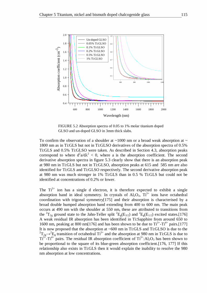
Chapter 5 Titanium, nickel and bismuth doped chalcogenide glass 115
Wavelength (nm)
600 800 1000 1200 1400 1600 1800 2000
Abs
orpt
ion
coe
ffici
ent
(cm
-1)
0.4
0.6
0.8
1.0
1.2
1.4
1.6
1.8
2.0
Un-doped GLSO0.05% Ti:GLSO0.1% Ti:GLSO0.2% Ti:GLSO0.5% Ti:GLSO1% Ti:GLSO
600 800 1000 1200
0.5
0.6
0.7
0.8
0.9
1.0
FIGURE 5.2 Absorption spectra of 0.05 to 1% molar titanium doped GLSO and un-doped GLSO in 3mm thick slabs.
To confirm the observation of a shoulder at ~1000 nm or a broad weak absorption at ~ 1800 nm as in Ti:GLS but not in Ti:GLSO derivatives of the absorption spectra of 0.5% Ti:GLS and 0.5% Ti:GLSO were taken. As described in Section 4.3, absorption peaks correspond to where d2a/dλ2 < 0, where a is the absorption coefficient. The second derivative absorption spectra in figure 5.3 clearly show that there is an absorption peak at 980 nm in Ti:GLS but not in Ti:GLSO, absorption peaks at 615 and 585 nm are also identified for Ti:GLS and Ti:GLSO respectively. The second derivative absorption peak at 980 nm was much stronger in 1% Ti:GLS than in 0.5 % Ti:GLS but could not be identified at concentrations of 0.2% or lower. The Ti3+ ion has a single d electron, it is therefore expected to exhibit a single absorption band in ideal symmetry. In crystals of Al2O3, Ti3+ ions have octahedral coordination with trigonal symmetry[175] and their absorption is characterised by a broad double humped absorption band extending from 400 to 600 nm. The main peak occurs at 490 nm with the shoulder at 550 nm, these are attributed to transitions from the 2T2g ground state to the Jahn-Teller split 2Eg(E3/2) and 2Eg(E1/2) excited states.[176] A weak residual IR absorption has been identified in Ti:Sapphire from around 650 to 1600 nm, peaking at 800 nm[176] and has been shown to be due to Ti3+-Ti4+ pairs.[177] It is now proposed that the absorption at ~600 nm in Ti:GLS and Ti:GLSO is due to the 2T2g→
2Eg transition of octahedral Ti3+ and the absorption at 980 nm in Ti:GLS is due to Ti3+-Ti4+ pairs. The residual IR absorption coefficient of Ti3+:Al2O3 has been shown to be proportional to the square of its blue-green absorption coefficient.[176, 177] If this relationship also exists in Ti:GLS then it would explain the inability to resolve the 980 nm absorption at low concentrations.

Chapter 5 Titanium, nickel and bismuth doped chalcogenide glass 116
Wavelength (nm)
800 1000 1200 1400 1600 1800 2000
d2 a/dλ
2
-8e-6
-6e-6
-4e-6
-2e-6
0
2e-6
4e-6 0.5% Ti:GLS
d2a/dλ2=0
0.5% Ti:GLSO
550 600 650 700 750 800
-0.0004
-0.0002
0.0000
0.0002
0.0004
0.0006
0.0008
FIGURE 5.3 Second derivative of the absorption coefficient of 0.5% Ti:GLS and 0.5% Ti:GLSO.
Because absorption due to Ti3+-Ti4+ pairs is detrimental to the performance of the Ti:Sapphire laser, much effort has been made to minimise it. In Ti:Sapphire the valence of Ti ions has been controlled by melting temperature and oxygen partial pressure[176, 178] In silica the concentration of Ti3+ relative to Ti4+ ([Ti3+]/[ Ti4+]) increased with melting temperature and decreasing oxygen partial pressure and was maximised by melting in deoxidized argon, i.e. a reducing atmosphere;[179] this is the same atmosphere that GLS is melted in so the oxygen partial pressure parameter is already maximised for the minimisation of Ti4+ concentration. In silicate, borate and phosphate glasses the redox reaction of TMm+↔TM(m+1)+ is related to the glass basicity (B),[88, 179] TM is a transition metal ion and glass basicity is calculated in terms of the coulombic force between the cation and oxygen ion of each glass component as in equation 5.1.[179]
( )2
4.1 2
×+
=i
ii Z
rB (5.1)
Where Zi and ri are the valency and radius of the cation, the values of 2 and 1.4 are the valency and radius of the oxygen ion respectively and Bi is the basicity of glass component i. The higher La2O3 content of GLSO compared to GLS is thought to cause the formation of oxide negative cavities[16] whereby the oxygen coordination of gallium is increased from 0 to 1, therefore GLSO should have a higher basicity than GLS. In silicate glass [Ti3+]/[ Ti4+] is inversely proportional to B, in borate glass [Ti3+]/[ Ti4+] is proportional to B and in phosphate glass there is no dependence of [Ti3+]/[ Ti4+] on B.[179] The relationship between [Ti3+]/[ Ti4+] and B in the GLS system is not known however it is assumed that [Ti3+]/[ Ti4+] is proportional to B since there is no absorption due to Ti3+-Ti4+ pairs in the more basic GLSO glass.

Chapter 5 Titanium, nickel and bismuth doped chalcogenide glass 117
The absorption of titanium has been characterised in a variety of glasses.[179-187] In all of the glasses a broad double humped absorption band extending from 400 to 750 nm was observed and attributed to Ti3+ in tetragonally distorted octahedron, except in silicate glass where a single absorption peak at 560 nm was observed and attributed to a continuous range of Jahn-Teller splittings. No absorption shoulder could be resolved in GLS and GLSO this is therefore attributed to the same effect. In some of the glasses an infrared absorption at ~800 nm was attributed to Ti3+-Ti4+ pairs. The peak absorptions for titanium in a variety of glasses and in sapphire are summarised in table 5.1
TABLE 5.1 Absorption details for titanium in a variety of glasses and in sapphire.
Host Ti3+
Absorption peak (nm)
Ti3+ Absorption shoulder (nm)
Ti3+-Ti4+ pair absorption peak
(nm)
Reference
GLS glass 615 - 980 This work
GLSO glass 585 - - This work
Sodium phosphor aluminate glass
560 697 - [188]
Silicate glass 560 - [186] Lithium calcium phosphate glass
510 680 - [185]
Lithium magnesium borate glass
515 679 - [180]
Sodium silicate glass 500 770 - [184] Phosphate glass 565 725 -
Barium borosilicate glass
500 746 - [187]
Lithium silicate glass
530 640 800 [179]
Sodium phosphor aluminate glass
580 650 - [179]
Fluorophosphate glass
529 685 - [183]
Al2O3 crystal 490 550 800 [176] 5.2.2 Photoluminescence of titanium doped GLS Photoluminescence spectra were taken using the setup described in section 3.3.2. In Ti:Al 2O3 emission peaks at ~750 nm when excited at 514 nm.[4] Out of all the titanium doped glasses in table 5.1 emission from d-d transitions in Ti3+ was only reported in sodium phosphor aluminate glass[188] in the other glasses emission was not investigated or not detectable. In Ti3+: sodium phosphor aluminate glass emission centred at 860 nm with a FWHM of 2020 cm-1 was detected from excitation with a 633 nm He-Ne laser. This is close to the emission of Ti:GLS and Ti:GLSO in figure 5.4 where the emission peaked at 900 nm when excited at the same wavelength. This further backs up the hypothesis that titanium is in a 3+ oxidation state in GLS and

Chapter 5 Titanium, nickel and bismuth doped chalcogenide glass 118
GLSO. The broadness of the PL spectrum indicates that the titanium ion is in a low crystal field site. No emission in the range 1200-1800 nm was detected from Ti:GLS when exciting with a CW 500 mW 1064 nm laser source.
Wavelength (nm)
800 900 1000 1100 1200 1300 1400 1500 1600 1700
Inte
nsity
(A
.U.)
0.0
0.5
1.0
1.5
2.0
2.5
3.0
0.1% Ti:GLS0.1% Ti:GLSO
FIGURE 5.4 Photoluminescence spectra of 0.1% titanium doped GLS and GLSO excited with a 5mW 633 nm laser source.
The observation that emission from Ti:GLS peaks at 900 nm, which is at a higher energy than the weak absorptions at 980 and 1700 nm, implies that these absorptions cannot be due to the same oxidation state and coordination of titanium that produced the emission and backs up the hypothesis that they are due to Ti3+-Ti4+ pairs. 5.2.3 Photoluminescence excitation of titanium doped GLS Photoluminescence excitation spectra were taken using the setup described in section 3.3.3. Figure 5.5 shows the excitation spectra of 0.1 % titanium doped GLS and GLSO, both of which show a single excitation peak at 580 nm which is in good agreement with the derivative absorption measurements. The excitation signal was relatively weak and the apparent increase in excitation in Ti:GLS at 800 nm is caused by correction for the system response. No excitation signal was detected up to 1000 nm, using a 600 line/mm grating to disperse the excitation source.
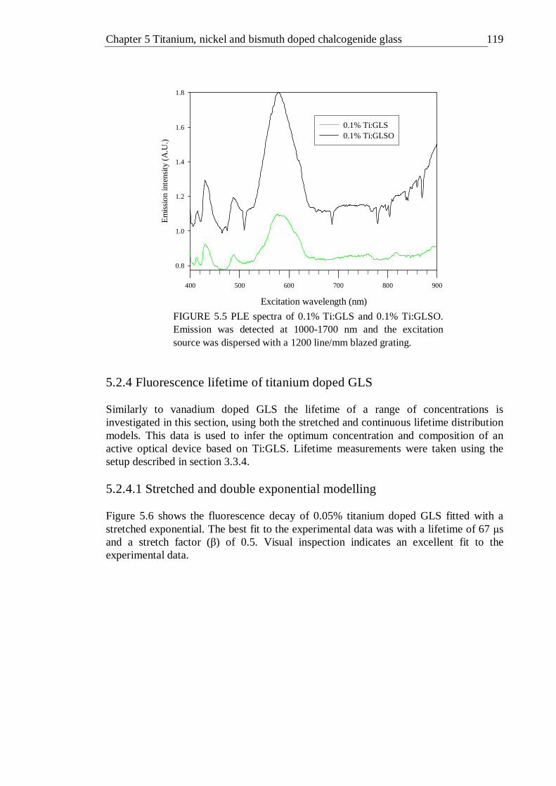
Chapter 5 Titanium, nickel and bismuth doped chalcogenide glass 119
Excitation wavelength (nm)
400 500 600 700 800 900
Em
issi
on
inte
nsity
(A
.U.)
0.8
1.0
1.2
1.4
1.6
1.8
0.1% Ti:GLS0.1% Ti:GLSO
FIGURE 5.5 PLE spectra of 0.1% Ti:GLS and 0.1% Ti:GLSO. Emission was detected at 1000-1700 nm and the excitation source was dispersed with a 1200 line/mm blazed grating.
5.2.4 Fluorescence lifetime of titanium doped GLS Similarly to vanadium doped GLS the lifetime of a range of concentrations is investigated in this section, using both the stretched and continuous lifetime distribution models. This data is used to infer the optimum concentration and composition of an active optical device based on Ti:GLS. Lifetime measurements were taken using the setup described in section 3.3.4. 5.2.4.1 Stretched and double exponential modelling Figure 5.6 shows the fluorescence decay of 0.05% titanium doped GLS fitted with a stretched exponential. The best fit to the experimental data was with a lifetime of 67 µs and a stretch factor (β) of 0.5. Visual inspection indicates an excellent fit to the experimental data.
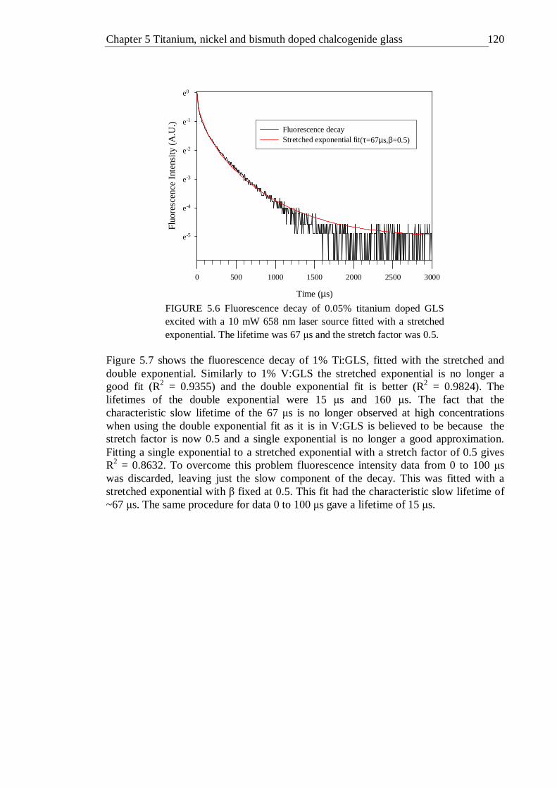
Chapter 5 Titanium, nickel and bismuth doped chalcogenide glass 120
Time (µs)
0 500 1000 1500 2000 2500 3000
Flu
ores
cenc
e In
tens
ity (
A.U
.)
e-5
e-4
e-3
e-2
e-1
e0
Fluorescence decay Stretched exponential fit(τ=67µs,β=0.5)
FIGURE 5.6 Fluorescence decay of 0.05% titanium doped GLS excited with a 10 mW 658 nm laser source fitted with a stretched exponential. The lifetime was 67 µs and the stretch factor was 0.5.
Figure 5.7 shows the fluorescence decay of 1% Ti:GLS, fitted with the stretched and double exponential. Similarly to 1% V:GLS the stretched exponential is no longer a good fit (R2 = 0.9355) and the double exponential fit is better (R2 = 0.9824). The lifetimes of the double exponential were 15 µs and 160 µs. The fact that the characteristic slow lifetime of the 67 µs is no longer observed at high concentrations when using the double exponential fit as it is in V:GLS is believed to be because the stretch factor is now 0.5 and a single exponential is no longer a good approximation. Fitting a single exponential to a stretched exponential with a stretch factor of 0.5 gives R2 = 0.8632. To overcome this problem fluorescence intensity data from 0 to 100 µs was discarded, leaving just the slow component of the decay. This was fitted with a stretched exponential with β fixed at 0.5. This fit had the characteristic slow lifetime of ~67 µs. The same procedure for data 0 to 100 µs gave a lifetime of 15 µs.
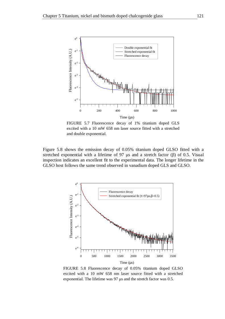
Chapter 5 Titanium, nickel and bismuth doped chalcogenide glass 121
Time (µs)
0 200 400 600 800 1000
Flu
ore
scen
ce I
nten
sity
(A
.U.)
e-5
e-4
e-3
e-2
e-1
e0
Double exponential fit Stretched exponential fit Fluorescence decay
FIGURE 5.7 Fluorescence decay of 1% titanium doped GLS excited with a 10 mW 658 nm laser source fitted with a stretched and double exponential.
Figure 5.8 shows the emission decay of 0.05% titanium doped GLSO fitted with a stretched exponential with a lifetime of 97 µs and a stretch factor (β) of 0.5. Visual inspection indicates an excellent fit to the experimental data. The longer lifetime in the GLSO host follows the same trend observed in vanadium doped GLS and GLSO.
Time (µs)
0 500 1000 1500 2000 2500 3000 3500
Flu
ore
sce
nce
Int
ens
ity (
A.U
.)
e-6
e-5
e-4
e-3
e-2
e-1
e0
Fluorescence decay Stretched exponential fit (τ=97µs,β=0.5)
FIGURE 5.8 Fluorescence decay of 0.05% titanium doped GLSO excited with a 10 mW 658 nm laser source fitted with a stretched exponential. The lifetime was 97 µs and the stretch factor was 0.5.
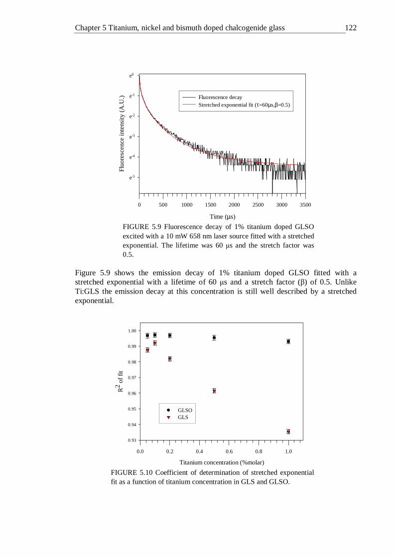
Chapter 5 Titanium, nickel and bismuth doped chalcogenide glass 122
Time (µs)
0 500 1000 1500 2000 2500 3000 3500
Flu
ore
sce
nce
inte
nsity
(A
.U.)
e-5
e-4
e-3
e-2
e-1
e0
Fluorescence decay Stretched exponential fit (τ=60µs,β=0.5)
FIGURE 5.9 Fluorescence decay of 1% titanium doped GLSO excited with a 10 mW 658 nm laser source fitted with a stretched exponential. The lifetime was 60 µs and the stretch factor was 0.5.
Figure 5.9 shows the emission decay of 1% titanium doped GLSO fitted with a stretched exponential with a lifetime of 60 µs and a stretch factor (β) of 0.5. Unlike Ti:GLS the emission decay at this concentration is still well described by a stretched exponential.
Titanium concentration (%molar)
0.0 0.2 0.4 0.6 0.8 1.0
R2 o
f fit
0.93
0.94
0.95
0.96
0.97
0.98
0.99
1.00
GLSOGLS
FIGURE 5.10 Coefficient of determination of stretched exponential fit as a function of titanium concentration in GLS and GLSO.
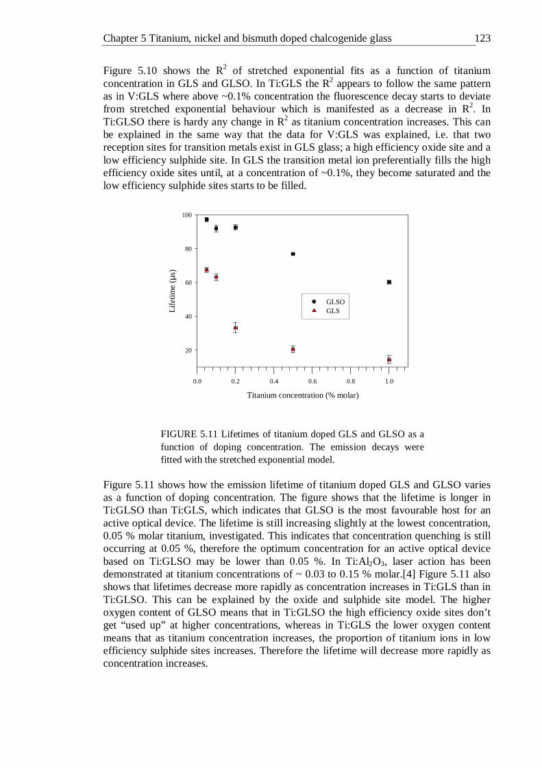
Chapter 5 Titanium, nickel and bismuth doped chalcogenide glass 123
Figure 5.10 shows the R2 of stretched exponential fits as a function of titanium concentration in GLS and GLSO. In Ti:GLS the R2 appears to follow the same pattern as in V:GLS where above ~0.1% concentration the fluorescence decay starts to deviate from stretched exponential behaviour which is manifested as a decrease in R2. In Ti:GLSO there is hardy any change in R2 as titanium concentration increases. This can be explained in the same way that the data for V:GLS was explained, i.e. that two reception sites for transition metals exist in GLS glass; a high efficiency oxide site and a low efficiency sulphide site. In GLS the transition metal ion preferentially fills the high efficiency oxide sites until, at a concentration of ~0.1%, they become saturated and the low efficiency sulphide sites starts to be filled.
Titanium concentration (% molar)
0.0 0.2 0.4 0.6 0.8 1.0
Life
time
(µs)
20
40
60
80
100
GLSOGLS
FIGURE 5.11 Lifetimes of titanium doped GLS and GLSO as a function of doping concentration. The emission decays were fitted with the stretched exponential model.
Figure 5.11 shows how the emission lifetime of titanium doped GLS and GLSO varies as a function of doping concentration. The figure shows that the lifetime is longer in Ti:GLSO than Ti:GLS, which indicates that GLSO is the most favourable host for an active optical device. The lifetime is still increasing slightly at the lowest concentration, 0.05 % molar titanium, investigated. This indicates that concentration quenching is still occurring at 0.05 %, therefore the optimum concentration for an active optical device based on Ti:GLSO may be lower than 0.05 %. In Ti:Al2O3, laser action has been demonstrated at titanium concentrations of ~ 0.03 to 0.15 % molar.[4] Figure 5.11 also shows that lifetimes decrease more rapidly as concentration increases in Ti:GLS than in Ti:GLSO. This can be explained by the oxide and sulphide site model. The higher oxygen content of GLSO means that in Ti:GLSO the high efficiency oxide sites don’t get “used up” at higher concentrations, whereas in Ti:GLS the lower oxygen content means that as titanium concentration increases, the proportion of titanium ions in low efficiency sulphide sites increases. Therefore the lifetime will decrease more rapidly as concentration increases.
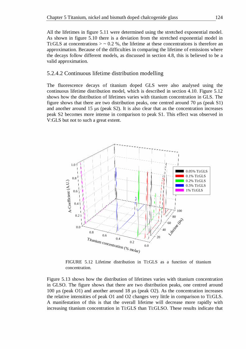
Chapter 5 Titanium, nickel and bismuth doped chalcogenide glass 124
All the lifetimes in figure 5.11 were determined using the stretched exponential model. As shown in figure 5.10 there is a deviation from the stretched exponential model in Ti:GLS at concentrations > ~ 0.2 %, the lifetime at these concentrations is therefore an approximation. Because of the difficulties in comparing the lifetime of emissions where the decays follow different models, as discussed in section 4.8, this is believed to be a valid approximation. 5.2.4.2 Continuous lifetime distribution modelling The fluorescence decays of titanium doped GLS were also analysed using the continuous lifetime distribution model, which is described in section 4.10. Figure 5.12 shows how the distribution of lifetimes varies with titanium concentration in GLS. The figure shows that there are two distribution peaks, one centred around 70 µs (peak S1) and another around 15 µs (peak S2). It is also clear that as the concentration increases peak S2 becomes more intense in comparison to peak S1. This effect was observed in V:GLS but not to such a great extent.
0.0
0.2
0.4
0.6
0.8
1.0
20
40
60
80
100
0.00.2
0.40.6
0.8
A-C
oeff
icie
nt (
A.U
.)
Life
time (
µs)
Titanium concentration (% molar)
0.05% Ti:GLS0.1% Ti:GLS0.2% Ti:GLS0.5% Ti:GLS1% Ti:GLS
FIGURE 5.12 Lifetime distribution in Ti:GLS as a function of titanium concentration.
Figure 5.13 shows how the distribution of lifetimes varies with titanium concentration in GLSO. The figure shows that there are two distribution peaks, one centred around 100 µs (peak O1) and another around 18 µs (peak O2). As the concentration increases the relative intensities of peak O1 and O2 changes very little in comparison to Ti:GLS. A manifestation of this is that the overall lifetime will decrease more rapidly with increasing titanium concentration in Ti:GLS than Ti:GLSO. These results indicate that
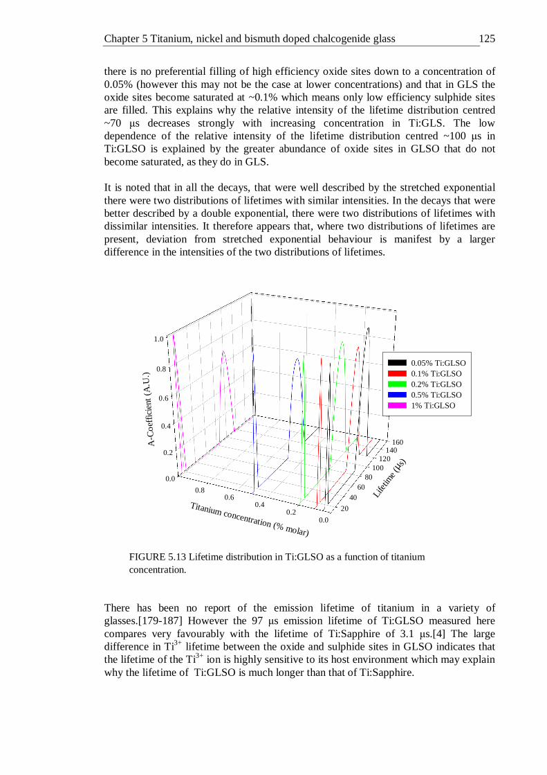
Chapter 5 Titanium, nickel and bismuth doped chalcogenide glass 125
there is no preferential filling of high efficiency oxide sites down to a concentration of 0.05% (however this may not be the case at lower concentrations) and that in GLS the oxide sites become saturated at ~0.1% which means only low efficiency sulphide sites are filled. This explains why the relative intensity of the lifetime distribution centred ~70 µs decreases strongly with increasing concentration in Ti:GLS. The low dependence of the relative intensity of the lifetime distribution centred ~100 µs in Ti:GLSO is explained by the greater abundance of oxide sites in GLSO that do not become saturated, as they do in GLS. It is noted that in all the decays, that were well described by the stretched exponential there were two distributions of lifetimes with similar intensities. In the decays that were better described by a double exponential, there were two distributions of lifetimes with dissimilar intensities. It therefore appears that, where two distributions of lifetimes are present, deviation from stretched exponential behaviour is manifest by a larger difference in the intensities of the two distributions of lifetimes.
0.0
0.2
0.4
0.6
0.8
1.0
20
4060
80100
120140
160
0.00.2
0.40.6
0.8
A-C
oeff
icie
nt (
A.U
.)
Life
time
(µs)
Titanium concentration (% molar)
0.05% Ti:GLSO0.1% Ti:GLSO0.2% Ti:GLSO0.5% Ti:GLSO1% Ti:GLSO
FIGURE 5.13 Lifetime distribution in Ti:GLSO as a function of titanium concentration.
There has been no report of the emission lifetime of titanium in a variety of glasses.[179-187] However the 97 µs emission lifetime of Ti:GLSO measured here compares very favourably with the lifetime of Ti:Sapphire of 3.1 µs.[4] The large difference in Ti3+ lifetime between the oxide and sulphide sites in GLSO indicates that the lifetime of the Ti3+ ion is highly sensitive to its host environment which may explain why the lifetime of Ti:GLSO is much longer than that of Ti:Sapphire.
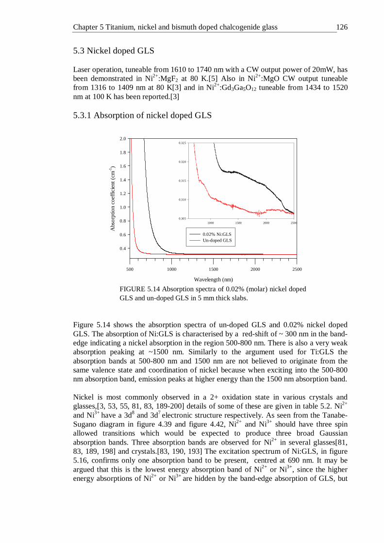
Chapter 5 Titanium, nickel and bismuth doped chalcogenide glass 126
5.3 Nickel doped GLS Laser operation, tuneable from 1610 to 1740 nm with a CW output power of 20mW, has been demonstrated in Ni2+:MgF2 at 80 K.[5] Also in Ni2+:MgO CW output tuneable from 1316 to 1409 nm at 80 K[3] and in Ni2+:Gd3Ga5O12 tuneable from 1434 to 1520 nm at 100 K has been reported.[3] 5.3.1 Absorption of nickel doped GLS
Wavelength (nm)
500 1000 1500 2000 2500
Abs
orp
tion
coef
ficie
nt (
cm-1)
0.4
0.6
0.8
1.0
1.2
1.4
1.6
1.8
2.0
0.02% Ni:GLSUn-doped GLS
1000 1500 2000 2500
0.305
0.310
0.315
0.320
0.325
FIGURE 5.14 Absorption spectra of 0.02% (molar) nickel doped GLS and un-doped GLS in 5 mm thick slabs.
Figure 5.14 shows the absorption spectra of un-doped GLS and 0.02% nickel doped GLS. The absorption of Ni:GLS is characterised by a red-shift of ~ 300 nm in the band-edge indicating a nickel absorption in the region 500-800 nm. There is also a very weak absorption peaking at ~1500 nm. Similarly to the argument used for Ti:GLS the absorption bands at 500-800 nm and 1500 nm are not believed to originate from the same valence state and coordination of nickel because when exciting into the 500-800 nm absorption band, emission peaks at higher energy than the 1500 nm absorption band. Nickel is most commonly observed in a 2+ oxidation state in various crystals and glasses,[3, 53, 55, 81, 83, 189-200] details of some of these are given in table 5.2. Ni2+ and Ni3+ have a 3d8 and 3d7 electronic structure respectively. As seen from the Tanabe-Sugano diagram in figure 4.39 and figure 4.42, Ni2+ and Ni3+ should have three spin allowed transitions which would be expected to produce three broad Gaussian absorption bands. Three absorption bands are observed for Ni2+ in several glasses[81, 83, 189, 198] and crystals.[83, 190, 193] The excitation spectrum of Ni:GLS, in figure 5.16, confirms only one absorption band to be present, centred at 690 nm. It may be argued that this is the lowest energy absorption band of Ni2+ or Ni3+, since the higher energy absorptions of Ni2+ or Ni3+ are hidden by the band-edge absorption of GLS, but
Chapter 5 Titanium, nickel and bismuth doped chalcogenide glass 127
in glasses with similar band-edge absorptions to GLS two absorption bands from Ni2+ are observed.[199] It is therefore thought unlikely that the absorption band of Ni:GLS centred at 690 nm is due to Ni2+ or Ni3+. The Ni+ ion has a 3d9 electronic structure, which is equivalent to a 3d1 electronic structure such as Ti3+, but the energy terms of its energy levels have negative crystal field components. Therefore, like Ti3+, Ni+ should exhibit one absorption band. Reports in the literature of Ni+ absorption are relatively scarce. In various hosts Ni+ displays a single absorption band between 1867 and 2611 nm.[201-203] These are all at lower energy than the absorption band in Ni:GLS, however they are all in tetrahedral symmetry. In octahedral coordination, ions are expected to display a higher energy absorption transition than in tetrahedral symmetry. It is therefore proposed that the 690 nm absorption of Ni:GLS is due to Ni+ in octahedral coordination. The weak absorption at ~1500 nm is attributed to small amounts of Ni+ in tetrahedral coordination. The weak absorption at ~1500 nm is not attributed to ion pairs such as Ni+-Ni2+, as in Ti:GLS, because, unlike Ti4+, Ni2+ is expected to contribute d-d absorption transitions.
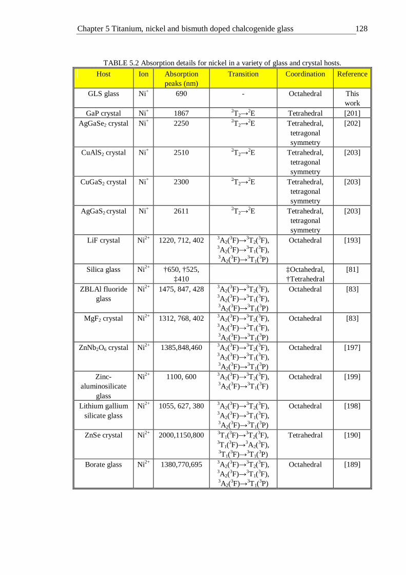
Chapter 5 Titanium, nickel and bismuth doped chalcogenide glass 128
TABLE 5.2 Absorption details for nickel in a variety of glass and crystal hosts.
Host Ion Absorption peaks (nm)
Transition Coordination Reference
GLS glass Ni+ 690 - Octahedral This work
GaP crystal Ni+ 1867 2T2→2E Tetrahedral [201]
AgGaSe2 crystal Ni+ 2250 2T2→2E Tetrahedral,
tetragonal symmetry
[202]
CuAlS2 crystal Ni+ 2510 2T2→2E Tetrahedral,
tetragonal symmetry
[203]
CuGaS2 crystal Ni+ 2300 2T2→2E Tetrahedral,
tetragonal symmetry
[203]
AgGaS2 crystal Ni+ 2611 2T2→2E Tetrahedral,
tetragonal symmetry
[203]
LiF crystal Ni2+ 1220, 712, 402 3A2(3F)→3T2(
3F), 3A2(
3F)→3T1(3F),
3A2(3F)→3T1(
3P)
Octahedral [193]
Silica glass Ni2+ †650, †525, ‡410
‡Octahedral, †Tetrahedral
[81]
ZBLAl fluoride glass
Ni2+ 1475, 847, 428 3A2(3F)→3T2(
3F), 3A2(
3F)→3T1(3F),
3A2(3F)→3T1(
3P)
Octahedral [83]
MgF2 crystal Ni2+ 1312, 768, 402 3A2(3F)→3T2(
3F), 3A2(
3F)→3T1(3F),
3A2(3F)→3T1(
3P)
Octahedral [83]
ZnNb2O6 crystal Ni2+ 1385,848,460 3A2(3F)→3T2(
3F), 3A2(
3F)→3T1(3F),
3A2(3F)→3T1(
3P)
Octahedral [197]
Zinc-aluminosilicate
glass
Ni2+ 1100, 600 3A2(3F)→3T2(
3F), 3A2(
3F)→3T1(3F)
Octahedral [199]
Lithium gallium silicate glass
Ni2+ 1055, 627, 380 3A2(3F)→3T2(
3F), 3A2(
3F)→3T1(3F),
3A2(3F)→3T1(
3P)
Octahedral [198]
ZnSe crystal Ni2+ 2000,1150,800 3T1(3F)→3T2(
3F), 3T1(
3F)→3A2(3F),
3T1(3F)→3T1(
3P)
Tetrahedral [190]
Borate glass Ni2+ 1380,770,695 3A2(3F)→3T2(
3F), 3A2(
3F)→3T1(3F),
3A2(3F)→3T1(
3P)
Octahedral [189]
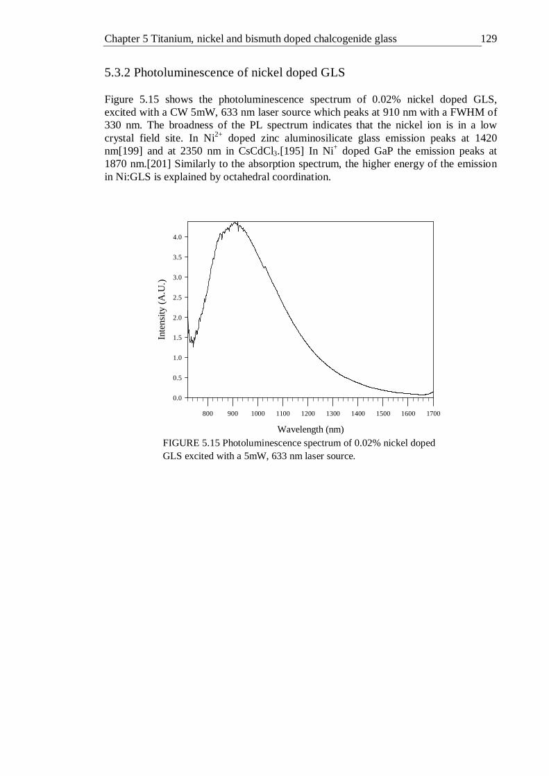
Chapter 5 Titanium, nickel and bismuth doped chalcogenide glass 129
5.3.2 Photoluminescence of nickel doped GLS Figure 5.15 shows the photoluminescence spectrum of 0.02% nickel doped GLS, excited with a CW 5mW, 633 nm laser source which peaks at 910 nm with a FWHM of 330 nm. The broadness of the PL spectrum indicates that the nickel ion is in a low crystal field site. In Ni2+ doped zinc aluminosilicate glass emission peaks at 1420 nm[199] and at 2350 nm in CsCdCl3.[195] In Ni+ doped GaP the emission peaks at 1870 nm.[201] Similarly to the absorption spectrum, the higher energy of the emission in Ni:GLS is explained by octahedral coordination.
Wavelength (nm)
800 900 1000 1100 1200 1300 1400 1500 1600 1700
Inte
nsity
(A
.U.)
0.0
0.5
1.0
1.5
2.0
2.5
3.0
3.5
4.0
FIGURE 5.15 Photoluminescence spectrum of 0.02% nickel doped GLS excited with a 5mW, 633 nm laser source.

Chapter 5 Titanium, nickel and bismuth doped chalcogenide glass 130
5.3.3 Photoluminescence excitation of nickel doped GLS Figure 5.16 shows the excitation spectra of 0.02% nickel doped GLS indicating a single absorption band centred at 690 nm. The increase in the excitation spectrum at ~450 nm was caused by the system correction.
Excitation wavelength (nm)
500 600 700 800 900 1000
Em
issi
on in
tens
ity (
A.U
.)
0.0
0.5
1.0
1.5
2.0
2.5
3.0
600 line/mm blazed grating1200 line/mm blazed grating
Figure 5.17 PLE spectra detecting emission at 1000-1700 nm of 0.02% nickel doped GLS.
5.3.4 Fluorescence lifetime of nickel doped GLS Figure 5.17 shows the fluorescence decay of 0.01% nickel doped GLS and GLSO, fitted with a stretched exponentials. The best fit to the experimental data was with lifetimes of 28 and 70 µs for GLS and GLSO hosts respectively. Similarly to vanadium and titanium there is an increase in lifetime in the GLSO host except the effect is more pronounced with nickel. These lifetimes compare to 400 µs, 300 µs, 583 µs and 240 µs for Ni2+ doped MgAl2O4,[55] Mg2SiO4,[200] zinc-aluminosilicate glass,[199] and Li2O-Ga2O3-SiO2 glass[198] respectively. Whereas the emission lifetime in Ni+ doped ZnS is 25 µs[204] These comparisons indicate a better match with the lifetime of Ni+.
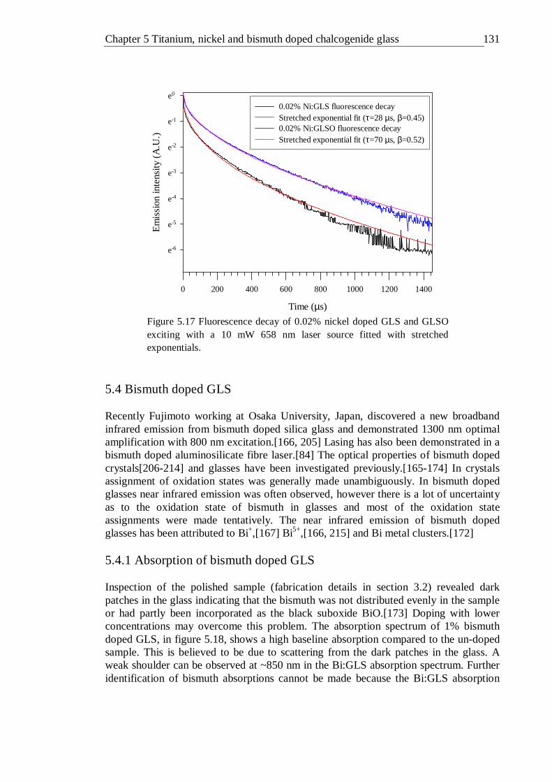
Chapter 5 Titanium, nickel and bismuth doped chalcogenide glass 131
Time (µs)
0 200 400 600 800 1000 1200 1400
Em
issi
on in
tens
ity (
A.U
.)
e-6
e-5
e-4
e-3
e-2
e-1
e0
0.02% Ni:GLS fluorescence decayStretched exponential fit (τ=28 µs, β=0.45)0.02% Ni:GLSO fluorescence decayStretched exponential fit (τ=70 µs, β=0.52)
Figure 5.17 Fluorescence decay of 0.02% nickel doped GLS and GLSO exciting with a 10 mW 658 nm laser source fitted with stretched exponentials.
5.4 Bismuth doped GLS Recently Fujimoto working at Osaka University, Japan, discovered a new broadband infrared emission from bismuth doped silica glass and demonstrated 1300 nm optimal amplification with 800 nm excitation.[166, 205] Lasing has also been demonstrated in a bismuth doped aluminosilicate fibre laser.[84] The optical properties of bismuth doped crystals[206-214] and glasses have been investigated previously.[165-174] In crystals assignment of oxidation states was generally made unambiguously. In bismuth doped glasses near infrared emission was often observed, however there is a lot of uncertainty as to the oxidation state of bismuth in glasses and most of the oxidation state assignments were made tentatively. The near infrared emission of bismuth doped glasses has been attributed to Bi+,[167] Bi5+,[166, 215] and Bi metal clusters.[172] 5.4.1 Absorption of bismuth doped GLS Inspection of the polished sample (fabrication details in section 3.2) revealed dark patches in the glass indicating that the bismuth was not distributed evenly in the sample or had partly been incorporated as the black suboxide BiO.[173] Doping with lower concentrations may overcome this problem. The absorption spectrum of 1% bismuth doped GLS, in figure 5.18, shows a high baseline absorption compared to the un-doped sample. This is believed to be due to scattering from the dark patches in the glass. A weak shoulder can be observed at ~850 nm in the Bi:GLS absorption spectrum. Further identification of bismuth absorptions cannot be made because the Bi:GLS absorption
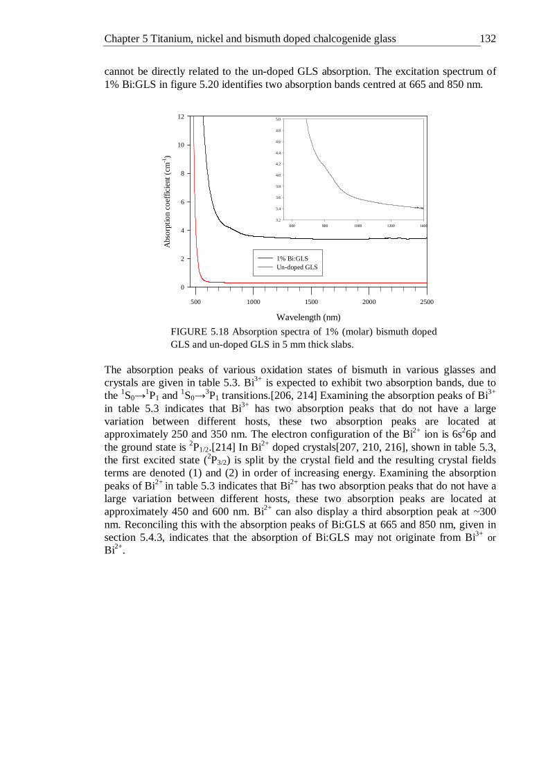
Chapter 5 Titanium, nickel and bismuth doped chalcogenide glass 132
cannot be directly related to the un-doped GLS absorption. The excitation spectrum of 1% Bi:GLS in figure 5.20 identifies two absorption bands centred at 665 and 850 nm.
Wavelength (nm)
500 1000 1500 2000 2500
Abs
orp
tion
coef
ficie
nt (
cm-1)
0
2
4
6
8
10
12
1% Bi:GLSUn-doped GLS
600 800 1000 1200 1400
3.2
3.4
3.6
3.8
4.0
4.2
4.4
4.6
4.8
5.0
FIGURE 5.18 Absorption spectra of 1% (molar) bismuth doped GLS and un-doped GLS in 5 mm thick slabs.
The absorption peaks of various oxidation states of bismuth in various glasses and crystals are given in table 5.3. Bi3+ is expected to exhibit two absorption bands, due to the 1S0→
1P1 and 1S0→3P1 transitions.[206, 214] Examining the absorption peaks of Bi3+
in table 5.3 indicates that Bi3+ has two absorption peaks that do not have a large variation between different hosts, these two absorption peaks are located at approximately 250 and 350 nm. The electron configuration of the Bi2+ ion is 6s26p and the ground state is 2P1/2.[214] In Bi2+ doped crystals[207, 210, 216], shown in table 5.3, the first excited state (2P3/2) is split by the crystal field and the resulting crystal fields terms are denoted (1) and (2) in order of increasing energy. Examining the absorption peaks of Bi2+ in table 5.3 indicates that Bi2+ has two absorption peaks that do not have a large variation between different hosts, these two absorption peaks are located at approximately 450 and 600 nm. Bi2+ can also display a third absorption peak at ~300 nm. Reconciling this with the absorption peaks of Bi:GLS at 665 and 850 nm, given in section 5.4.3, indicates that the absorption of Bi:GLS may not originate from Bi3+ or Bi2+.
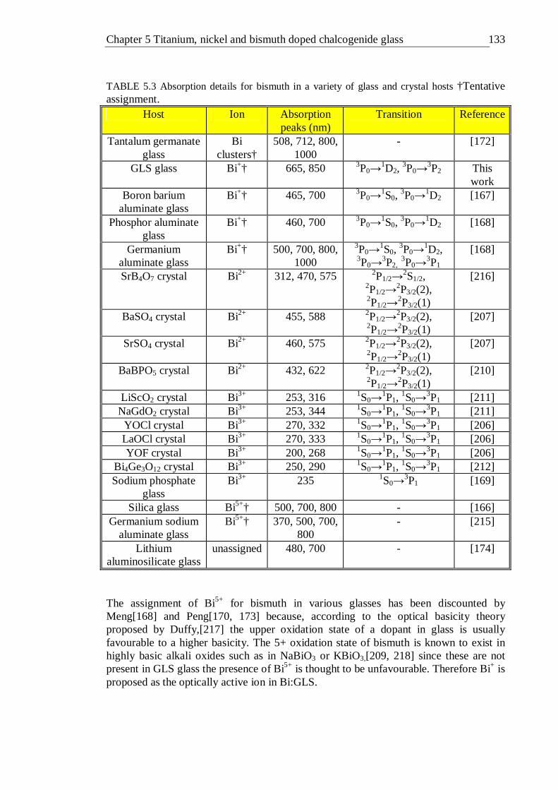
Chapter 5 Titanium, nickel and bismuth doped chalcogenide glass 133
TABLE 5.3 Absorption details for bismuth in a variety of glass and crystal hosts †Tentative assignment.
Host Ion Absorption peaks (nm)
Transition Reference
Tantalum germanate glass
Bi clusters†
508, 712, 800, 1000
- [172]
GLS glass Bi+† 665, 850 3P0→1D2,
3P0→3P2
This work
Boron barium aluminate glass
Bi+† 465, 700 3P0→1S0,
3P0→1D2 [167]
Phosphor aluminate glass
Bi+† 460, 700 3P0→1S0,
3P0→1D2 [168]
Germanium aluminate glass
Bi+† 500, 700, 800, 1000
3P0→1S0,
3P0→1D2,
3P0→3P2,
3P0→3P1
[168]
SrB4O7 crystal Bi2+ 312, 470, 575 2P1/2→2S1/2,
2P1/2→2P3/2(2),
2P1/2→2P3/2(1)
[216]
BaSO4 crystal Bi2+ 455, 588 2P1/2→2P3/2(2),
2P1/2→2P3/2(1)
[207]
SrSO4 crystal Bi2+ 460, 575 2P1/2→2P3/2(2),
2P1/2→2P3/2(1)
[207]
BaBPO5 crystal Bi2+ 432, 622 2P1/2→2P3/2(2),
2P1/2→2P3/2(1)
[210]
LiScO2 crystal Bi3+ 253, 316 1S0→1P1,
1S0→3P1 [211]
NaGdO2 crystal Bi3+ 253, 344 1S0→1P1,
1S0→3P1 [211]
YOCl crystal Bi3+ 270, 332 1S0→1P1,
1S0→3P1
[206] LaOCl crystal Bi3+ 270, 333 1S0→
1P1, 1S0→
3P1 [206]
YOF crystal Bi3+ 200, 268 1S0→1P1,
1S0→3P1
[206] Bi4Ge3O12 crystal Bi3+ 250, 290 1S0→
1P1, 1S0→
3P1 [212] Sodium phosphate
glass Bi3+ 235 1S0→
3P1 [169]
Silica glass Bi5+† 500, 700, 800 - [166] Germanium sodium
aluminate glass Bi5+† 370, 500, 700,
800 - [215]
Lithium aluminosilicate glass
unassigned 480, 700 - [174]
The assignment of Bi5+ for bismuth in various glasses has been discounted by Meng[168] and Peng[170, 173] because, according to the optical basicity theory proposed by Duffy,[217] the upper oxidation state of a dopant in glass is usually favourable to a higher basicity. The 5+ oxidation state of bismuth is known to exist in highly basic alkali oxides such as in NaBiO3 or KBiO3,[209, 218] since these are not present in GLS glass the presence of Bi5+ is thought to be unfavourable. Therefore Bi+ is proposed as the optically active ion in Bi:GLS.
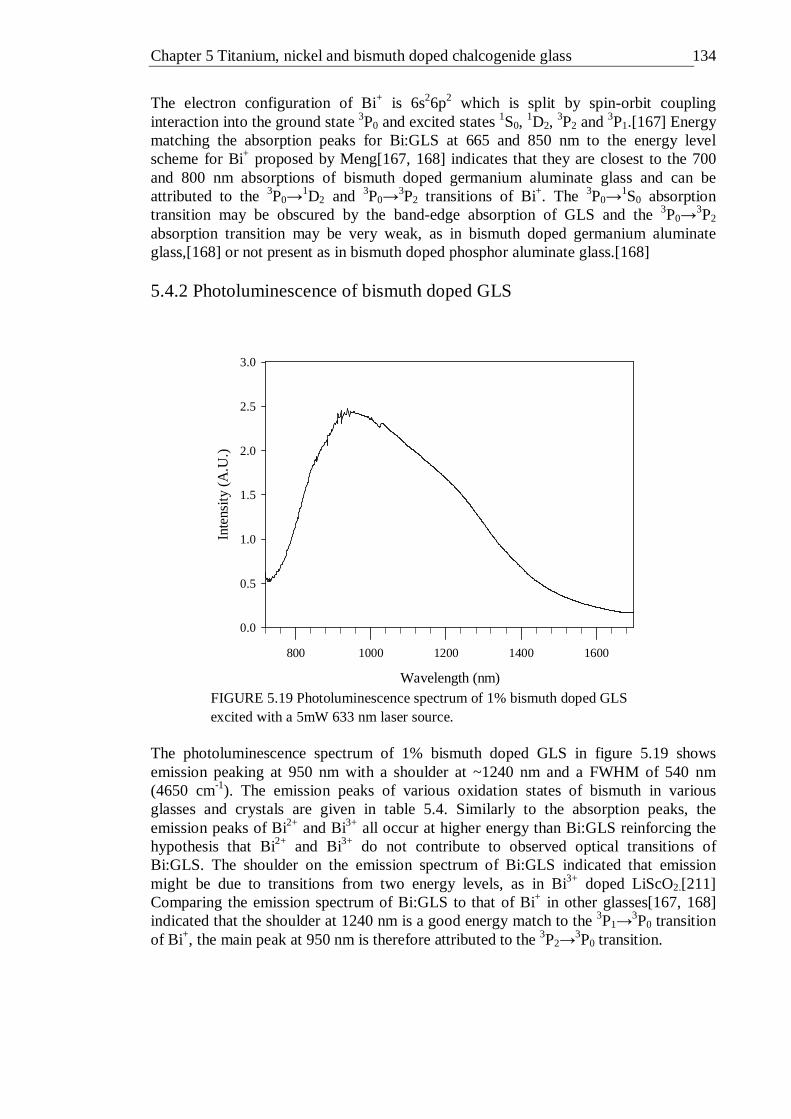
Chapter 5 Titanium, nickel and bismuth doped chalcogenide glass 134
The electron configuration of Bi+ is 6s26p2 which is split by spin-orbit coupling interaction into the ground state 3P0 and excited states 1S0,
1D2, 3P2 and 3P1.[167] Energy
matching the absorption peaks for Bi:GLS at 665 and 850 nm to the energy level scheme for Bi+ proposed by Meng[167, 168] indicates that they are closest to the 700 and 800 nm absorptions of bismuth doped germanium aluminate glass and can be attributed to the 3P0→
1D2 and 3P0→3P2 transitions of Bi+. The 3P0→
1S0 absorption transition may be obscured by the band-edge absorption of GLS and the 3P0→
3P2 absorption transition may be very weak, as in bismuth doped germanium aluminate glass,[168] or not present as in bismuth doped phosphor aluminate glass.[168] 5.4.2 Photoluminescence of bismuth doped GLS
Wavelength (nm)
800 1000 1200 1400 1600
Inte
nsity
(A
.U.)
0.0
0.5
1.0
1.5
2.0
2.5
3.0
FIGURE 5.19 Photoluminescence spectrum of 1% bismuth doped GLS excited with a 5mW 633 nm laser source.
The photoluminescence spectrum of 1% bismuth doped GLS in figure 5.19 shows emission peaking at 950 nm with a shoulder at ~1240 nm and a FWHM of 540 nm (4650 cm-1). The emission peaks of various oxidation states of bismuth in various glasses and crystals are given in table 5.4. Similarly to the absorption peaks, the emission peaks of Bi2+ and Bi3+ all occur at higher energy than Bi:GLS reinforcing the hypothesis that Bi2+ and Bi3+ do not contribute to observed optical transitions of Bi:GLS. The shoulder on the emission spectrum of Bi:GLS indicated that emission might be due to transitions from two energy levels, as in Bi3+ doped LiScO2.[211] Comparing the emission spectrum of Bi:GLS to that of Bi+ in other glasses[167, 168] indicated that the shoulder at 1240 nm is a good energy match to the 3P1→
3P0 transition of Bi+, the main peak at 950 nm is therefore attributed to the 3P2→
3P0 transition.

Chapter 5 Titanium, nickel and bismuth doped chalcogenide glass 135
TABLE 5.4 Emission details for bismuth in a variety of glass and crystal hosts †Tentative assignment.
Host Ion Emission peaks (nm)
Transition Reference
Tantalum germanate glass
Bi clusters†
1310 - [172]
Boron barium aluminate glass
Bi+† 1148 3P1→3P0 [167]
Phosphor aluminate glass Bi+† 1300 3P1→3P0 [168]
Germanium aluminate glass
Bi+† 1300 3P1→3P0 [168]
GLS glass Bi+† 950, 1240 3P2→3P0,
3P1→3P0
This work
SrB4O7 crystal Bi2+ 585 2P3/2(1)→2P1/2 [216] BaSO4 crystal Bi2+ 625 2P3/2(1)→2P1/2 [207] BaSO4 crystal Bi2+ 640 2P3/2(1)→2P1/2 [207] LiScO2 crystal Bi3+ 404 3P1→
1S0, 3P0→
1S0 [211]
NaGdO2 crystal Bi3+ 384 3P1→1S0,
3P0→1S0
[211]
YOCl crystal Bi3+ 400 3P1→1S0
[206] LaOCl crystal Bi3+ 345 3P1→
1S0 [206]
YOF crystal Bi3+ 330 3P1→1S0
[206] Bi4Ge3O12 crystal Bi3+ 475 3P1→
1S0 [212] Sodium phosphate glass Bi3+ 400 3P1→
1S0 [169]
Silica glass Bi5+† 750-1250 - [166] Germanium sodium
aluminate glass Bi5+† 1220 - [215]
Lithium aluminosilicate glass
unassigned 1100, 1350 - [174]
In Bi3+ doped LiScO2 and NaGdO2, excitation took place into the 3P1 level but emission was observed from both the 3P1→1S0 transition and the spin forbidden 3P0→
1S0
transition. In bismuth doped silica glass infrared emission was only observed with aluminium codopant,[166] it also varied with excitation wavelength with two emission peaks at 750 and 1140 nm under 500 nm excitation, one at 1122 nm under 700 nm excitation and one at 1250 nm under 800 nm excitation. In bismuth doped lithium aluminosilicate glass, emission consisted of two Gaussian peaks at 1100 and 1350 nm, these peaks had lifetimes of 549 and 270 µs respectively. No infrared emission from Bi3+ and no fluorescence lifetime from Bi3+ longer than 5 µs has been reported.[173]

Chapter 5 Titanium, nickel and bismuth doped chalcogenide glass 136
5.4.3 Photoluminescence excitation of bismuth doped GLS Photoluminescence excitation spectra were taken using the setup described in section 3.3.3. The excitation spectrum of 1% Bi:GLS, in figure 5.20, shows a peak at 850 nm which can be related to the weak shoulder of the absorption spectrum in figure 5.18 and a peak at 665 nm which could not be resolved in the absorption measurement.
Excitation wavelength (nm)
500 600 700 800 900 1000
Em
issi
on in
tens
ity (
A.U
.)
0.0
0.5
1.0
1.5
2.0
2.5
600 line/mm blazed grating1200 line/mm blazed grating
FIGURE 5.20 PLE spectra detecting emission at 1000-1700 nm of 1% bismuth doped GLS.

Chapter 5 Titanium, nickel and bismuth doped chalcogenide glass 137
5.4.4 Fluorescence lifetime of bismuth doped GLS
Time (µs)
0 100 200 300 400
Em
issi
on in
tens
ity (
A.U
.)
e-9
e-8
e-7
e-6
e-5
e-4
e-3
e-2
e-1
e0
1% Bi:GLS fluorescence decayDouble exponential fit (τ1= 6.5 µs, τ2= 60 µs)
Continuous lifetime distribution fit
FIGURE 5.21 Fluorescence decay of 1% bismuth doped GLS exciting with a CW 10 mW, 658 nm laser source and fitted with a double exponential and the continuous lifetime distribution model.
Figure 5.21 shows the fluorescence decay of 1% bismuth doped GLS. Likewise to similar concentrations of vanadium and titanium doped GLS the decay did not follow stretched exponential behaviour and was more accurately described by a double exponential. The lifetimes of the double exponential fit were 6.5 and 60 µs. The decay was also fitted using the continuous lifetime distribution model (see section 4.10). The results are given in figure 5.22 and show two lifetime distributions centred at 7 and 47 µs, which is in reasonable agreement with the results of the double exponential fit. Two lifetime components have been reported for bismuth doped glasses[165, 171] which were attributed to the bismuth ion occupying different sites in the glasses. This may be the case for Bi:GLS since, as described in section 4.7, it is thought that transition metals occupy oxide and sulphide sites which give rise to long and short lifetime respectively. However, the shoulder in the emission spectrum indicates that two energy levels may be involved in the emission so the two lifetime components may be the lifetimes of the two energy levels as in Bi3+ doped LiScO2. [211]

Chapter 5 Titanium, nickel and bismuth doped chalcogenide glass 138
Lifetime (µs)
10 20 30 40 50 60 70 80
A-C
oeffi
cien
t (A
.U.)
0.00
0.05
0.10
0.15
0.20
FIGURE 5.22 Lifetime distribution in the emission decay of 1% bismuth doped GLS.
The emission lifetimes of various oxidation states of bismuth in various glasses and crystals are given in table 5.5. The lifetime for Bi:GLS is longer than the reported lifetimes for Bi3+, again reinforcing the hypothesis that Bi3+ does not contribute to observed optical transitions of Bi:GLS. The lifetime for Bi:GLS is longer than the reported lifetimes for Bi+ and bismuth doped glasses in which optical gain and lasing were demonstrated, however lowering the concentration and using GLSO host may significantly increase the lifetime. The emission lifetime and emission cross section are important parameters for the characterisation of a laser material because the laser threshold is inversely proportional to the product of the emission lifetime and emission cross section.[130] However, calculation of the emission cross section requires determination of the quantum efficiency. This was not possible for Bi:GLS because of the loss of ORC facilities, see section 1.5, therefore quantum efficiency measurements of Bi:GLS is suggested as further work.

Chapter 5 Titanium, nickel and bismuth doped chalcogenide glass 139
TABLE 5.5 Emission lifetime details for bismuth in a variety of glass and crystal hosts †Tentative assignment ‡Lasing demonstrated.
Host Ion Lifetime (µs) Transition Reference GLS glass Bi+† 7, 47 3P2→
3P0, 3P1→
3P0 This work
Tantalum germanate
glass
Bi clusters† 200 - [172]
Boron barium aluminate glass
Bi+† 350 3P1→3P0 [167]
Aluminosilicate glass
unassigned‡ 1000 - [84]
Phosphor aluminate glass
Bi+† 500 3P1→3P0 [168]
LiScO2 crystal Bi3+ 0.045, 380 3P1→1S0,
3P0→1S0 [211]
NaGdO2 crystal Bi3+ 0.1, 7 3P1→1S0,
3P0→1S0 [211]
YOCl crystal Bi3+ 1.4 3P1→1S0
[206] LaOCl crystal Bi3+ 1.6 3P1→
1S0 [206]
Bi4Ge3O12 crystal
Bi3+ 0.4 3P1→1S0 [212]
Sodium phosphate glass
Bi3+ 3.9 3P1→1S0
[169]
Germanium sodium
aluminate glass
Bi5+† 434 - [215]
Silica glass Bi5+† 630 - [166] 5.5 Conclusions Absorption measurements of Ti:GLS identified an absorption band at ~500-600 nm that could not be fully resolved because of its proximity to the band-edge of GLS. At concentrations of 0.5% and greater a shoulder at ~1000 nm is observed, there is also a weak and broad absorption centred at around 1800 nm. The second derivative absorption spectra identified an absorption peak at 980 nm in Ti:GLS but not in Ti:GLSO, absorption peaks at 615 and 585 nm are also identified for Ti:GLS and Ti:GLSO respectively. The excitation spectra of 0.1% titanium doped GLS and GLSO both show a single excitation peak at 580 nm The emission spectra of Ti:GLS and Ti:GLSO both peaked at 900 nm. It is proposed that the absorption at ~600 nm in Ti:GLS and Ti:GLSO is due to the 2T2g→
2Eg transition of octahedral Ti3+ and the absorption at 980 nm in Ti:GLS is due to Ti3+-Ti4+ pairs. The 97 µs emission lifetime of Ti:GLSO compares very favourably to the lifetime of Ti:Sapphire of 3.1 µs. The optimum doping concentration for an active device based on Ti:GLSO may be lower than the lowest concentration of 0.05 % molar investigated in this chapter. Therefore the investigation of lower doping concentrations of Ti:GLSO is suggested as further work. The fabrication of a Ti:GLSO fibre at the optimum doping concentration for applications as a tuneable laser source is also suggested as further work.

Chapter 5 Titanium, nickel and bismuth doped chalcogenide glass 140
The absorption of Ni:GLS is characterised by a red-shift of ~ 300 nm in the band-edge indicating a nickel absorption in the region 500-800 nm. There is also a very weak absorption peaking at ~1500 nm. The excitation spectra of Ni:GLS indicate a single absorption band centred at 690 nm. It is proposed that the 690 nm absorption of Ni:GLS is due to Ni+ in octahedral coordination. The weak absorption at ~1500 nm is attributed to small amounts of Ni+ in tetrahedral coordination. The photoluminescence spectrum peaks at 910 nm with a FWHM of 330 nm. The lifetimes of Ni:GLS and Ni:GLSO are 28 and 70 µs respectively. Fabrication of a range of concentrations of Ni:GLS and Ni:GLSO to further investigate its spectroscopic properties is suggested as further work. A weak shoulder can be observed at ~850 nm in the Bi:GLS absorption spectrum. Further identification of bismuth absorptions cannot be made because dark patches in the sample were detrimental to its absorption. The excitation spectrum of Bi:GLS shows peaks at 665 and 850 nm Based on comparisons to other work the absorption peaks for Bi:GLS at 665 and 850 nm are attributed to the 3P0→
1D2 and 3P0→3P2 transitions of Bi+.
The emission decay of Bi:GLS consisted of two lifetime distributions centred at 7 and 47 µs. The demonstration of lasing in bismuth doped aluminosilicate glass makes development of a Bi:GLS laser more favourable. Fabrication of a range of concentrations of Bi:GLS and Bi:GLSO to further investigate its spectroscopic properties is suggested as further work.
Chapter 6 Femtosecond laser written waveguides in chalcogenide glass 141
Chapter 6
Femtosecond laser written waveguides in chalcogenide glass 6.1 Introduction In this chapter the fabrication and characterisation of buried waveguides written into GLS glass using 800 nm focused fs laser pulses is reported. The spectral broadening of 1550 nm fs laser pulses coupled into these waveguides is also reported. 6.1.1 Femtosecond laser material modification Femtosecond (fs) lasers have several advantages over conventional laser systems for the micro-structuring of transparent dielectrics. These include the reduction of collateral damage[219] and sub-diffraction limited ablation.[220-222] In gold film 800 nm fs lasers have been used to ablate holes roughly 10% of the focus spot size.[223] This effect was attributed to the minimised thermal diffusion time of ultra-short pulses that have a peak laser fluence slightly above a well defined ablation threshold.[223] Femtosecond laser modification of transparent solids has many potential applications. The possibility of writing active devices has been demonstrated in Er-Yb doped silicate glass.[224] Plasma-induced bulk modification by the tightly focused fs lasers has been demonstrated as a tool for three-dimensional optical memory with data storage capacities of up to 1016 bits/m3.[225-228] Tightly focused fs lasers have also been used for micro-structuring in transparent dielectrics.[229, 230] Infra-red femtosecond laser pulses have be used to permanently photo-reduce Eu3+ to Eu2+ in fluorozirconate glass,[231] photo-oxidation of Mn2+ to Mn3+ has also been observed in silicate glass.[230] 6.1.2 Highly nonlinear glass Highly nonlinear glass is an excellent candidate material for optical, ultrafast, nonlinear devices such as demultiplexers,[232] wavelength converters[233] and optical Kerr shutters.[234] This is because of its ability to cause nonlinear phase shifts over much shorter interaction lengths than conventional (silica based) devices. Various waveguiding structures such as fibres, proton beam written waveguides, continuous wave (CW) laser written waveguides and fs laser written waveguides could be used to realise such devices. Of these, fs laser writing is particularly attractive because, as well as having rapid processing times, waveguiding structures can be formed below the surface of the glass enabling 3-D structures to be fabricated. Optical components such as a Fresnel zone plate[235] and a fibre attenuator[230] have been fabricated using fs laser pulses. Several studies have described the fabrication and characterisation of waveguides using focused fs laser pulses in phosphate glass[236] chalcogenide glass[237] and heavy metal oxide glass.[238] Of these chalcogenide glasses are especially attractive because they have a high nonlinear refractive index and enhanced IR transmission, coupled with low maximum phonon energy. The nonlinear refractive index of chalcogenide glasses is in general higher than oxide glasses with the same

Chapter 6 Femtosecond laser written waveguides in chalcogenide glass 142
linear refractive index. This is believed to be a consequence of the large polarizability of the chalcogen ions.[239] Of the chalcogenide glasses, gallium lanthanum sulphide (GLS) is probably the most notable, with respect to optical nonlinear devices, as it has a nonlinear figure of merit (FOM) of >7, which is believed to be the highest for any bulk glass reported to date,[240]
λβTPA
nFOM
22= (6.1)
where λ is the wavelength, n2 is the real part of the nonlinear refractive index and βTPA is the two-photon absorption (TPA) coefficient. 6.1.3 Nonlinear optical devices A potential use for waveguides written, in highly nonlinear glass such as GLS, is the realisation of nonlinear optical devices. A long term goal of the work presented in this chapter is the possibility of fabricating an optical chip using fs laser writing that could incorporate optical amplification and ultra fast switching integrated on a single device. What follows is a brief description of various optical devices that exploit the nonlinear properties of waveguiding structures. 6.1.3.1 Mach-Zehnder interferometer switch The basic principle of a Mach-Zehnder interferometer switch is that guided light is split into two branches of a waveguiding structure and then recombined at an output in such a way that interference can occur. By inducing a π, or odd multiple of π, phase shift in one of the branches the recombined beams can interfere destructively. Devices have been demonstrated in which a π phase shift is induced on a 1520 nm, 1 fJ signal pulse with a width of 150 fs, through the saturation of a semiconductor optical amplifier (SOA) by a 250 fJ control pulse with the same wavelength and pulse width as the signal pulse.[241] In other devices a π phase shift was induced by applying a voltage to InGaAlAs/InAlAs waveguide structure.[242] 6.1.3.2 Optical Kerr shutters Optical Kerr shutters exploit the nonlinear phase induced by the intensity dependent nonlinear birefringence to change the state of polarization (SOP) of a weak signal in a nonlinear medium.[243] These devices are often realised in a fibre geometry, in this case a linearly polarised signal is launched into a polarisation maintaining fibre polarized at 45° to both the two principal axes. The SOP of the signal changes periodically due to birefringence built into the fibre. The original SOP is restored by a quarter-wave plate at the output of the fibre and is then blocked by a crossed polarizer, this is the closed state of the optical Kerr shutter. To open the shutter, linearly polarized strong pump light is launched along one of the two principle axes of the fibre together with the signal. In this case the refractive indices for the parallel and perpendicular components of the signal become slightly different, with respect to the direction of the pump polarization, due to the pump induced birefringence. This nonlinear birefringence
Chapter 6 Femtosecond laser written waveguides in chalcogenide glass 143
causes a nonlinear phase shift and also changes the SOP of the signal, thus the signal is transmitted through the polarizer.[243] A switching power of 3W has been demonstrated for an optical Kerr shutter based on 1.2 m of As2S3 fibre.[244] Optical Kerr shutters have been used for various applications such as intensity discrimination[245] and optical sampling.[234] 6.1.3.3 2R regenerator An all-optical signal regeneration technique utilizing self-phase modulation (SPM) in fibre and subsequent filtering of the signal was first proposed by Mamyshev.[246] This is a 2R regenerator (where 2R stands for re-amplification and re-shaping) simply comprising of a nonlinear waveguide and an optical bandpass filter. This method is based on the effect of SPM of the data signal in a nonlinear medium with subsequent optical filtering at a frequency ωf, which is shifted with respect to the input data carrier frequency ω0.[246] Due to the effects of SPM the input pulse broadens to ∆ωSPM, given by equation 6.2 (also given in section 6.4.4.2) [246]
λπω
ωLIn p
SPM20 2∆
=∆ (6.2)
Where ∆ω0 is the bandwidth of the input pulse, n2 is the nonlinear refractive index, Ip is the pulse intensity, L is the waveguide length and λ is the wavelength. After the nonlinear waveguide, the pulse passes through an optical filter with centre frequency ωf, shifted from the signal frequency ω0 given by: ωf = ω0 + ∆ωshift. If ∆ωSPM/2< ∆ωshift the input pulse is rejected by the filter, this happens when the pulse intensity Ip is too small (noise in “zeros”). If the pulse intensity is high enough so that ∆ωSPM/2≥ ∆ωshift, a part of the SPM broadened pulse passes through the filter.[246] Since the spectral density of the broadened spectrum at the filter pass band can be made to be relatively insensitive to the peak power of the input pulses, any amplitude fluctuations in “one” bits are reduced by the process.[247] 6.2 Waveguide fabrication and characterisation techniques 6.2.1 Waveguide fabrication Waveguides were written in two different samples; these were a GLS and a GLSO sample, both having dimensions of ~ 12x12x5 mm. The GLS sample was prepared by mixing 65% gallium sulphide, 30% lanthanum sulphide and 5% lanthanum oxide (% molar) and the GLSO sample was prepared by mixing 77.5% gallium sulphide and 22.5% lanthanum oxide (% molar). The batching and melting details for these glasses are given in section 3.2.1. After the waveguides were written their enfaces were polished to a scratch-dig surface quality of 40-20 and a parallelism of < 0.03°. The first digits of the scratch-dig specification relate to the maximum width allowance of a scratch in µm, the next digits indicate the maximum diameter allowance for a dig in 1/100 mm. A schematic of the waveguide writing process is shown in figure 6.1. Femto second laser radiation was generated using a Coherent system comprising of a Mira mode

Chapter 6 Femtosecond laser written waveguides in chalcogenide glass 144
locked Ti:Sapphire oscillator which was pumped by a Verdi V10 frequency doubled ,10W, 532 nm diode pumped laser. The output of the Mira seeded a RegA 9000 regenerative amplifier which was tuned to 800 nm and emitted a train of pulses with a duration of 150 fs, a repetition rate of 250 KHz and a pulse energy up to 6µJ. A mirror diverted the output of the RegA to the direct write setup where a computer controlled shutter regulated the irradiation time. Pulse energy was controlled using a variable neutral density filter and a half wave plate allowed rotation of the linear laser polarisation. The lenses L1 and L2 were used to reduce the beam radius so that it had a high coupling efficiency into the objective. The laser beam was focused via a 50x objective (NA=0.55) at 100-400 µm below the surface of the sample. The focus spot diameter was measured to be 1.5 µm in air and calculated to be around 2 µm inside the glass sample. The sample was mounted on a Aerotech computer controlled, linear motor, translation stage which could move in 3 axes with a resolution of a 20 nm in all three axes. A series of channels at various pulse energies and translation velocities was written in the sample by translating it perpendicularly to the propagation direction of the laser beam. A red glow attributed to plasma fluorescence, see section 6.3, was visible from the focal point as it passed through the sample. After processing, the end faces of the sample were polished for subsequent characterisation.
Mira
RegA 9000
50XNA=0.55
800 nm (150 fs)
532 nm (CW)Verdi V10
532 nm (CW)Verdi V18
nJ, 700-980 nm
µJ, 750-850 nm
ShutterL1 L2
Iris ND filter
λ/2 plate
IrisSample
3D stage
CCDcamera
x
yz
Translationdirection
FIGURE 6.1 Schematic of waveguide writing process.
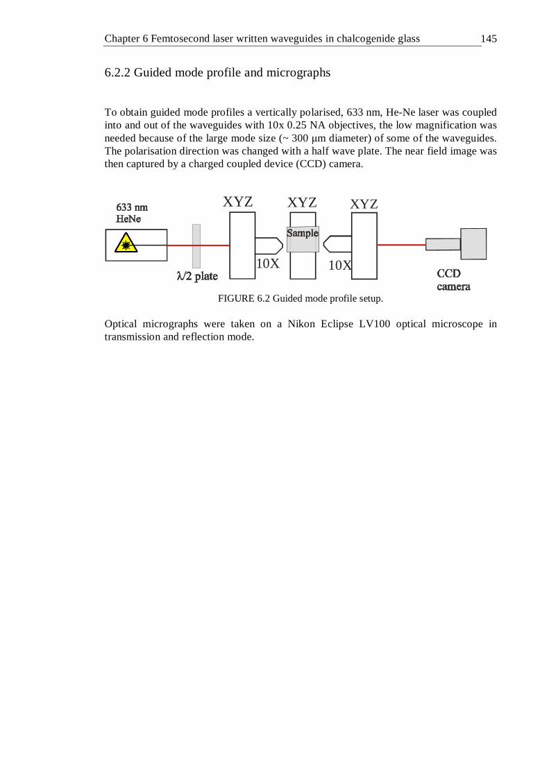
Chapter 6 Femtosecond laser written waveguides in chalcogenide glass 145
6.2.2 Guided mode profile and micrographs To obtain guided mode profiles a vertically polarised, 633 nm, He-Ne laser was coupled into and out of the waveguides with 10x 0.25 NA objectives, the low magnification was needed because of the large mode size (~ 300 µm diameter) of some of the waveguides. The polarisation direction was changed with a half wave plate. The near field image was then captured by a charged coupled device (CCD) camera.
XYZXYZ XYZ
10X10X
FIGURE 6.2 Guided mode profile setup.
Optical micrographs were taken on a Nikon Eclipse LV100 optical microscope in transmission and reflection mode.
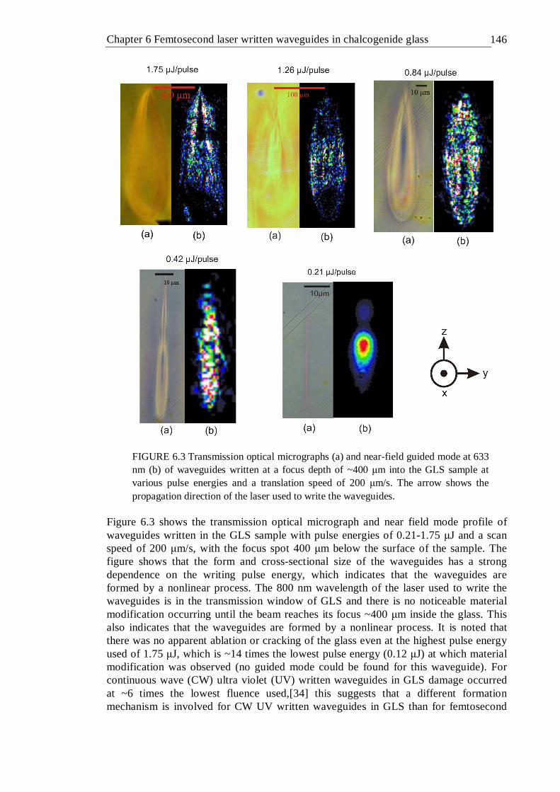
Chapter 6 Femtosecond laser written waveguides in chalcogenide glass 146
FIGURE 6.3 Transmission optical micrographs (a) and near-field guided mode at 633 nm (b) of waveguides written at a focus depth of ~400 µm into the GLS sample at various pulse energies and a translation speed of 200 µm/s. The arrow shows the propagation direction of the laser used to write the waveguides.
Figure 6.3 shows the transmission optical micrograph and near field mode profile of waveguides written in the GLS sample with pulse energies of 0.21-1.75 µJ and a scan speed of 200 µm/s, with the focus spot 400 µm below the surface of the sample. The figure shows that the form and cross-sectional size of the waveguides has a strong dependence on the writing pulse energy, which indicates that the waveguides are formed by a nonlinear process. The 800 nm wavelength of the laser used to write the waveguides is in the transmission window of GLS and there is no noticeable material modification occurring until the beam reaches its focus ~400 µm inside the glass. This also indicates that the waveguides are formed by a nonlinear process. It is noted that there was no apparent ablation or cracking of the glass even at the highest pulse energy used of 1.75 µJ, which is ~14 times the lowest pulse energy (0.12 µJ) at which material modification was observed (no guided mode could be found for this waveguide). For continuous wave (CW) ultra violet (UV) written waveguides in GLS damage occurred at ~6 times the lowest fluence used,[34] this suggests that a different formation mechanism is involved for CW UV written waveguides in GLS than for femtosecond
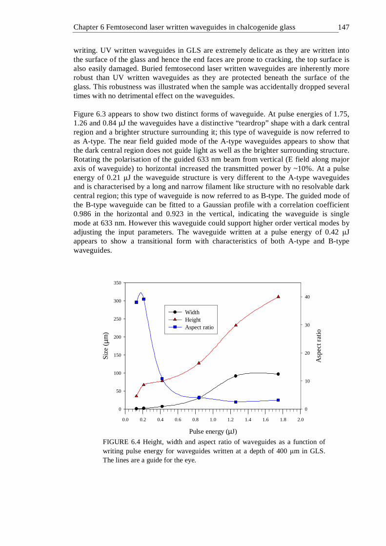
Chapter 6 Femtosecond laser written waveguides in chalcogenide glass 147
writing. UV written waveguides in GLS are extremely delicate as they are written into the surface of the glass and hence the end faces are prone to cracking, the top surface is also easily damaged. Buried femtosecond laser written waveguides are inherently more robust than UV written waveguides as they are protected beneath the surface of the glass. This robustness was illustrated when the sample was accidentally dropped several times with no detrimental effect on the waveguides. Figure 6.3 appears to show two distinct forms of waveguide. At pulse energies of 1.75, 1.26 and 0.84 µJ the waveguides have a distinctive “teardrop” shape with a dark central region and a brighter structure surrounding it; this type of waveguide is now referred to as A-type. The near field guided mode of the A-type waveguides appears to show that the dark central region does not guide light as well as the brighter surrounding structure. Rotating the polarisation of the guided 633 nm beam from vertical (E field along major axis of waveguide) to horizontal increased the transmitted power by ~10%. At a pulse energy of 0.21 µJ the waveguide structure is very different to the A-type waveguides and is characterised by a long and narrow filament like structure with no resolvable dark central region; this type of waveguide is now referred to as B-type. The guided mode of the B-type waveguide can be fitted to a Gaussian profile with a correlation coefficient 0.986 in the horizontal and 0.923 in the vertical, indicating the waveguide is single mode at 633 nm. However this waveguide could support higher order vertical modes by adjusting the input parameters. The waveguide written at a pulse energy of 0.42 µJ appears to show a transitional form with characteristics of both A-type and B-type waveguides.
Pulse energy (µJ)
0.0 0.2 0.4 0.6 0.8 1.0 1.2 1.4 1.6 1.8 2.0
Siz
e ( µ
m)
0
50
100
150
200
250
300
350
Asp
ect
ra
tio
0
10
20
30
40
WidthHeightAspect ratio
FIGURE 6.4 Height, width and aspect ratio of waveguides as a function of writing pulse energy for waveguides written at a depth of 400 µm in GLS. The lines are a guide for the eye.
Chapter 6 Femtosecond laser written waveguides in chalcogenide glass 148
The height (z dimension), width (y dimension) and aspect ratio (height/width) measured for these waveguides are shown in figure 6.4. Comparing the aspect ratio of the waveguides to their type indicates that A-type waveguides are characterised by an aspect ratio of 3-5 and B-type waveguides are characterised by an aspect ratio of ~40. The width of the waveguides reaches a maximum of ~100 µm at a pulse energy of ~1.2 µJ whereas the height of the waveguides continues to increase up to the maximum pulse energy used. The top of the waveguides were all at the same depth in the glass but as the pulse energy was increased the waveguides moved towards the source of the writing laser beam. Figure 6.5 shows the transmission optical micrograph, near-field guided mode and reflection optical micrograph of waveguides written in the GLS sample at pulse energies between 0.28 and 0.4 µJ, translation speeds of 200, 100 and 50 µm/s at a focus depth of 100 µm below the surface of the sample. Similarly to figure 6.3, the transmission optical micrograph shows a “teardrop” shape with a dark central region (now referred to as region 1) and a brighter structure surrounding it (now referred to as region 2), however this differentiation of structure is clearer than for the waveguides in figure 6.3. It is also more apparent that region 1 does not actively guide light and it is only region 2 that guides light. This effect is probably related to the depth that the waveguides were written at and may arise from the lower resistance to expansion caused by exposure to the fs laser pulses at the lesser depth. It could also be caused by a greater aberration in the writing beam for the waveguides written at a depth of 400 µm than at 100 µm, caused by imperfections and inhomogeneities in the glass. The reflection optical micrograph shows that region 2 has a high reflectivity indicating that it has undergone a positive refractive index change; region 1 has a lower reflectivity indicating that it has undergone a lower refractive index change. The waveguides in figure 6.5 are all A-type and comparing the size of the waveguides in figure 6.6 to those in figure 6.4 shows that for similar pulse energies the waveguides written at a depth of 100 µm are wider than those written at a depth of 400 µm, although they are not as high because the waveguides written at a depth of 400 µm are B-type or a transitional form. This indicates that there is some attenuation of the writing laser beam as it is transmitted through the glass before it reaches a focus and undergoes non-linear absorption. Comparing the size and form of the waveguides in figure 6.5, written at translation speeds 200, 100 and 50 µm/s shows that the waveguides written at these speeds are virtually identical for the same pulse energy with a slight increase in size as the speed decreases. For the various pulse energies used there is a 10-20% increase in width and a 5-10% increase in height going from a translation speed of 200 µm/s to 50 µm/s. This small increase in size, with a quadrupling of the writing beam fluence on the sample, indicates that the absorption and thermalisation process caused by each pulse is almost complete when the next pulse arrives 4 µs later.
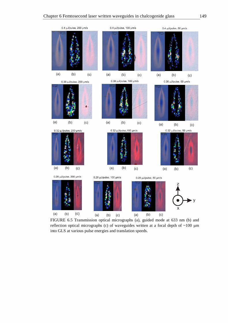
Chapter 6 Femtosecond laser written waveguides in chalcogenide glass 149
FIGURE 6.5 Transmission optical micrographs (a), guided mode at 633 nm (b) and reflection optical micrographs (c) of waveguides written at a focal depth of ~100 µm into GLS at various pulse energies and translation speeds.
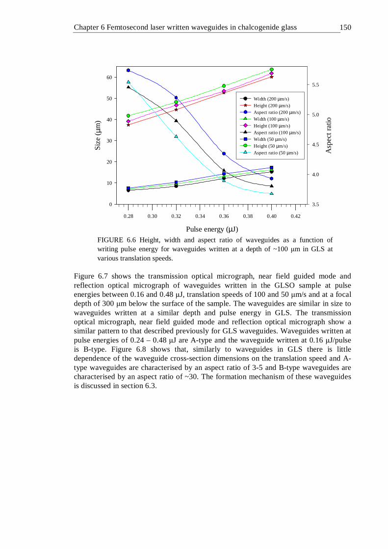
Chapter 6 Femtosecond laser written waveguides in chalcogenide glass 150
Pulse energy (µJ)
0.28 0.30 0.32 0.34 0.36 0.38 0.40 0.42
Siz
e ( µm
)
0
10
20
30
40
50
60
Asp
ect
ra
tio
3.5
4.0
4.5
5.0
5.5
Width (200 µm/s) Height (200 µm/s)Aspect ratio (200 µm/s)Width (100 µm/s)Height (100 µm/s)Aspect ratio (100 µm/s)Width (50 µm/s)Height (50 µm/s)Aspect ratio (50 µm/s)
FIGURE 6.6 Height, width and aspect ratio of waveguides as a function of writing pulse energy for waveguides written at a depth of ~100 µm in GLS at various translation speeds.
Figure 6.7 shows the transmission optical micrograph, near field guided mode and reflection optical micrograph of waveguides written in the GLSO sample at pulse energies between 0.16 and 0.48 µJ, translation speeds of 100 and 50 µm/s and at a focal depth of 300 µm below the surface of the sample. The waveguides are similar in size to waveguides written at a similar depth and pulse energy in GLS. The transmission optical micrograph, near field guided mode and reflection optical micrograph show a similar pattern to that described previously for GLS waveguides. Waveguides written at pulse energies of 0.24 – 0.48 µJ are A-type and the waveguide written at 0.16 µJ/pulse is B-type. Figure 6.8 shows that, similarly to waveguides in GLS there is little dependence of the waveguide cross-section dimensions on the translation speed and A-type waveguides are characterised by an aspect ratio of 3-5 and B-type waveguides are characterised by an aspect ratio of ~30. The formation mechanism of these waveguides is discussed in section 6.3.
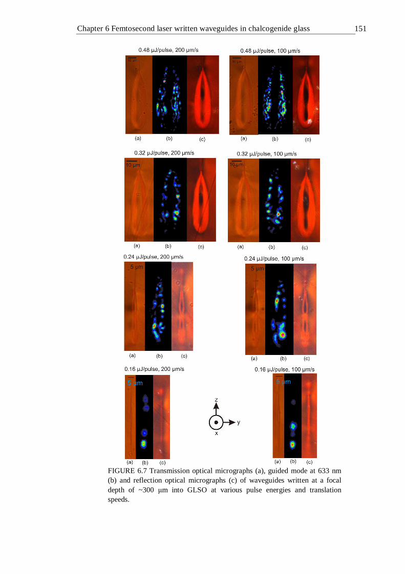
Chapter 6 Femtosecond laser written waveguides in chalcogenide glass 151
FIGURE 6.7 Transmission optical micrographs (a), guided mode at 633 nm (b) and reflection optical micrographs (c) of waveguides written at a focal depth of ~300 µm into GLSO at various pulse energies and translation speeds.
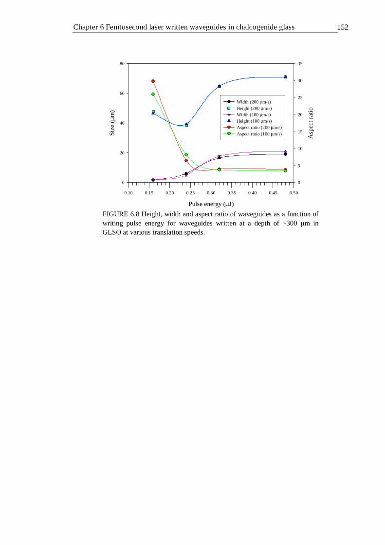
Chapter 6 Femtosecond laser written waveguides in chalcogenide glass 152
Pulse energy (µJ)
0.10 0.15 0.20 0.25 0.30 0.35 0.40 0.45 0.50
Siz
e ( µ
m)
0
20
40
60
80
Asp
ect r
atio
0
5
10
15
20
25
30
35
Width (200 µm/s) Height (200 µm/s)Width (100 µm/s)Height (100 µm/s)Aspect ratio (200 µm/s)
Aspect ratio (100 µm/s)
FIGURE 6.8 Height, width and aspect ratio of waveguides as a function of writing pulse energy for waveguides written at a depth of ~300 µm in GLSO at various translation speeds.
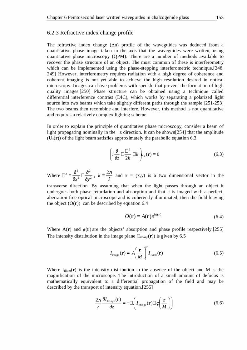
Chapter 6 Femtosecond laser written waveguides in chalcogenide glass 153
6.2.3 Refractive index change profile The refractive index change (∆n) profile of the waveguides was deduced from a quantitative phase image taken in the axis that the waveguides were written, using quantitative phase microscopy (QPM). There are a number of methods available to recover the phase structure of an object. The most common of these is interferometry which can be implemented using the phase-stepping interferometric technique.[248, 249] However, interferometry requires radiation with a high degree of coherence and coherent imaging is not yet able to achieve the high resolution desired in optical microscopy. Images can have problems with speckle that prevent the formation of high quality images.[250] Phase structure can be obtained using a technique called differential interference contrast (DIC), which works by separating a polarized light source into two beams which take slightly different paths through the sample.[251-253] The two beams then recombine and interfere. However, this method is not quantitative and requires a relatively complex lighting scheme. In order to explain the principle of quantitative phase microscopy, consider a beam of light propagating nominally in the +z direction. It can be shown[254] that the amplitude (Uz(r)) of the light beam satisfies approximately the parabolic equation 6.3.
0)(2
2
=
+∇+
∂∂
rzukkz
i (6.3)
Where 2
2
2
22
yx ∂∂+
∂∂=∇ ,
λπ2=k and r = (x,y) is a two dimensional vector in the
transverse direction. By assuming that when the light passes through an object it undergoes both phase retardation and absorption and that it is imaged with a perfect, aberration free optical microscope and is coherently illuminated; then the field leaving the object (O(r)) can be described by equation 6.4
)()()( rrr φieAO = (6.4) Where A(r) and )(rφ are the objects’ absorption and phase profile respectively.[255] The intensity distribution in the image plane (Iimage(r)) is given by 6.5
)()(2
rr
r Illumimage IM
AI
= (6.5)
Where Iillum(r) is the intensity distribution in the absence of the object and M is the magnification of the microscope. The introduction of a small amount of defocus is mathematically equivalent to a differential propagation of the field and may be described by the transport of intensity equation.[255]
∇−∇=∂
∂M
Iz
Iage
age rr
rφ
λπ
)(.)(2
ImIm (6.6)

Chapter 6 Femtosecond laser written waveguides in chalcogenide glass 154
Given the availability of positively and negatively defocused images, equation 6.6 can be solved for the phase using Fourier transform methods.[256] This analysis is based on coherent illumination, however, the optical microscopes used in QPM systems use a partially coherent illumination source. It can be shown[255] that a partially coherent source gives an identical result to the coherent case, in equation 6.6, provided that the irradiance distribution of the illumination source shows inversion symmetry.[255] After the phase has been found, the refractive index change (∆n) of the waveguides can be calculated using equation 6.7.[257]
dn
πφλ2
=∆ (6.7)
Where λ is the wavelength of 550 nm used by IATIA software to calculate the quantitative phase image and d is the height (z dimension) of the waveguides. The QPM system used here is illustrated in figure 6.9 and incorporated an Olympus BX51 optical microscope equipped with a Physik Instrumente P721K039, nano-focusing, Z drive with a resolution of < 1 nm to take in-focus and very slightly positively and negatively defocused images. IATIA software was then used to calculate the quantitative phase image.
FIGURE 6.9 Quantitative phase microscopy setup.
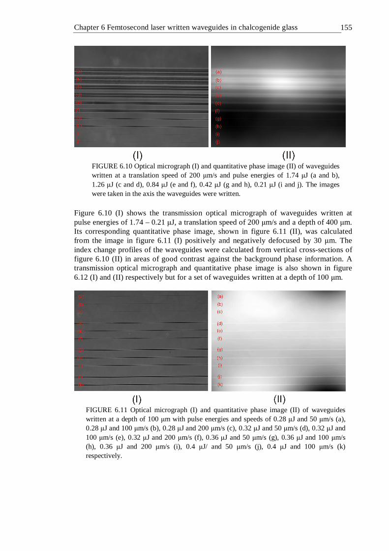
Chapter 6 Femtosecond laser written waveguides in chalcogenide glass 155
FIGURE 6.10 Optical micrograph (I) and quantitative phase image (II) of waveguides written at a translation speed of 200 µm/s and pulse energies of 1.74 µJ (a and b), 1.26 µJ (c and d), 0.84 µJ (e and f), 0.42 µJ (g and h), 0.21 µJ (i and j). The images were taken in the axis the waveguides were written.
Figure 6.10 (I) shows the transmission optical micrograph of waveguides written at pulse energies of 1.74 – 0.21 µJ, a translation speed of 200 µm/s and a depth of 400 µm. Its corresponding quantitative phase image, shown in figure 6.11 (II), was calculated from the image in figure 6.11 (I) positively and negatively defocused by 30 µm. The index change profiles of the waveguides were calculated from vertical cross-sections of figure 6.10 (II) in areas of good contrast against the background phase information. A transmission optical micrograph and quantitative phase image is also shown in figure 6.12 (I) and (II) respectively but for a set of waveguides written at a depth of 100 µm.
FIGURE 6.11 Optical micrograph (I) and quantitative phase image (II) of waveguides written at a depth of 100 µm with pulse energies and speeds of 0.28 µJ and 50 µm/s (a), 0.28 µJ and 100 µm/s (b), 0.28 µJ and 200 µm/s (c), 0.32 µJ and 50 µm/s (d), 0.32 µJ and 100 µm/s (e), 0.32 µJ and 200 µm/s (f), 0.36 µJ and 50 µm/s (g), 0.36 µJ and 100 µm/s (h), 0.36 µJ and 200 µm/s (i), 0.4 µJ/ and 50 µm/s (j), 0.4 µJ and 100 µm/s (k) respectively.

Chapter 6 Femtosecond laser written waveguides in chalcogenide glass 156
The quantitative phase map in figure 6.11 (II) was used to emulate a differential interference contrast (DIC) image, shown in figure 6.12, which illustrates the excellent image quality available through DIC. Although the DIC image does not contain quantitative phase information it has enhanced contrast and resolution and a reduced number of artefacts.
FIGURE 6.12 Emulated differential interference contrast image from quantitative phase image in figure 6.12 II.
An example of the phase profiles extracted from figure 6.10 (II) and 6.11 (II) is shown in figure 6.13. The background phase profile was assumed to vary linearly over the width of the waveguide. This linear approximation was then subtracted from the phase change profile to give the phase profile for the waveguide alone.
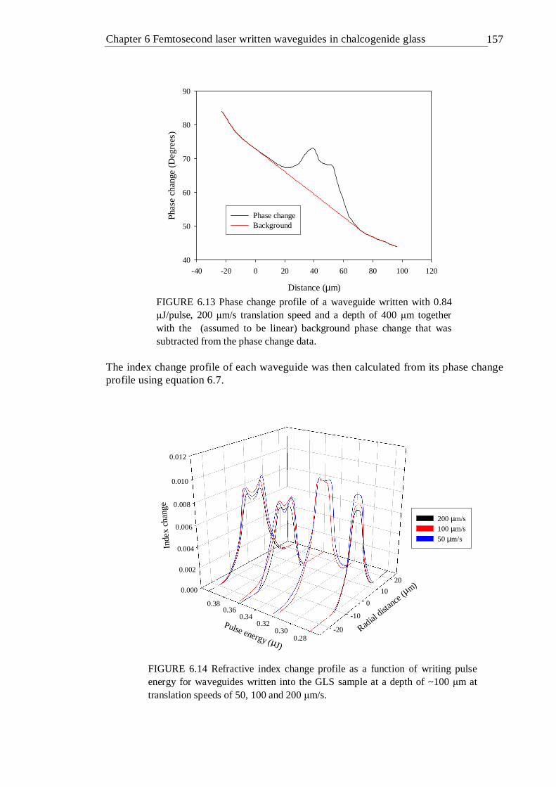
Chapter 6 Femtosecond laser written waveguides in chalcogenide glass 157
Distance (µm)
-40 -20 0 20 40 60 80 100 120
Pha
se c
hang
e (D
egre
es)
40
50
60
70
80
90
Phase changeBackground
FIGURE 6.13 Phase change profile of a waveguide written with 0.84 µJ/pulse, 200 µm/s translation speed and a depth of 400 µm together with the (assumed to be linear) background phase change that was subtracted from the phase change data.
The index change profile of each waveguide was then calculated from its phase change profile using equation 6.7.
0.000
0.002
0.004
0.006
0.008
0.010
0.012
-20
-10
0
10
20
0.280.30
0.320.34
0.360.38
Inde
x ch
ange
Radial
distan
ce (µm)
Pulse energy (µJ)
200 µm/s100 µm/s50 µm/s
FIGURE 6.14 Refractive index change profile as a function of writing pulse energy for waveguides written into the GLS sample at a depth of ~100 µm at translation speeds of 50, 100 and 200 µm/s.

Chapter 6 Femtosecond laser written waveguides in chalcogenide glass 158
Figure 6.14 shows the refractive index change (∆n) profile as a function of writing pulse energy for waveguides written into the GLS sample at a depth of ~100 µm at translation speeds of 50, 100 and 200 µm/s; the figure shows a double peak structure with a trough at the centre for waveguides written at pulse energies of 0.36 and 0.4 µJ. Comparing the ∆n profile of the waveguides written at pulse energies of 0.36 and 0.4 µJ to their optical micrographs, in figure 6.5, demonstrates that region 1 has undergone a lower refractive index change than region 2 but whether the index change of region 1 is negative is still unclear. Figure 6.15 shows the ∆n profile of a waveguide written with a pulse energy of 0.4 µJ and a translation speed of 50 µm/s superimposed onto its transmission optical micrograph. This clarifies that region 1 has undergone a lower refractive index change than region 2, it also indicates that the index variation extends beyond the visible boundary of the waveguide. Examining the micrographs of the waveguides (figures 6.3, 6.5 and 6.7) shows that the waveguides tend to get narrower moving away from the centre of the waveguide (zero radial distance), the index change profiles will therefore be an underestimated distance away from the centre of the waveguide. Because the visible boundary of the waveguide may not represent the boundary of the index modulation, taking into account the change in waveguide thickness with radial distance may be unproductive. The ∆n profile in the middle of the waveguide includes the index change of region 1 and 2, decoupling the index change for both these regions to determine if region 1 has undergone a negative index change required the boundaries of these regions to be accurately defined. As previously discussed, defining the boundaries of the different waveguide regions is difficult. However, using the waveguide shown in figure 6.15 and approximating the waveguide regions by eye, the waveguide thickness at the peak index change of 8.6x10⁻³ is ~ 69% of the maximum waveguide thickness, giving a peak index change of 1.24x10⁻², all of this index change is due to region 2. The thickness of region 2 in the centre of the waveguide is ~ 38% of the maximum waveguide thickness, therefore the index change due to region 2 in the centre of the waveguide should be 38/69x1.24x10-2 = 7.0x10⁻³. This value is slightly higher than the observed index change of 6.7x10⁻³ and indicates that region 1 has undergone a negative index change of 3x10⁻⁴. However, region 1 could show a positive index change, depending on how the boundaries of region 1 and 2 are defined, therefore a more systematic way of defining the boundaries is required. Ellipsometry measurements of the waveguide end faces should be able to directly measure the index change of regions 1 and 2, these measurements were attempted but they failed to reveal any index variation, the reason for this is unclear.
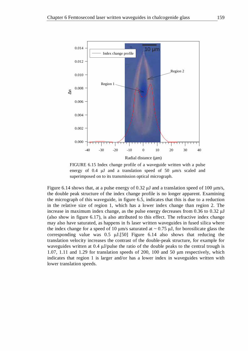
Chapter 6 Femtosecond laser written waveguides in chalcogenide glass 159
10 mµ
Radial distance (µm)
-40 -30 -20 -10 0 10 20 30 40
∆n
0.000
0.002
0.004
0.006
0.008
0.010
0.012
0.014
Index change profile
Region 1
Region 2
FIGURE 6.15 Index change profile of a waveguide written with a pulse energy of 0.4 µJ and a translation speed of 50 µm/s scaled and superimposed on to its transmission optical micrograph.
Figure 6.14 shows that, at a pulse energy of 0.32 µJ and a translation speed of 100 µm/s, the double peak structure of the index change profile is no longer apparent. Examining the micrograph of this waveguide, in figure 6.5, indicates that this is due to a reduction in the relative size of region 1, which has a lower index change than region 2. The increase in maximum index change, as the pulse energy decreases from 0.36 to 0.32 µJ (also show in figure 6.17), is also attributed to this effect. The refractive index change may also have saturated, as happens in fs laser written waveguides in fused silica where the index change for a speed of 10 µm/s saturated at ~ 0.75 µJ, for borosilicate glass the corresponding value was 0.5 µJ.[50] Figure 6.14 also shows that reducing the translation velocity increases the contrast of the double-peak structure, for example for waveguides written at 0.4 µJ/pulse the ratio of the double peaks to the central trough is 1.07, 1.11 and 1.29 for translation speeds of 200, 100 and 50 µm respectively, which indicates that region 1 is larger and/or has a lower index in waveguides written with lower translation speeds.

Chapter 6 Femtosecond laser written waveguides in chalcogenide glass 160
0.000
0.002
0.004
0.006
0.008
0.010
-60
-40
-20
0
2040
0.20.4
0.60.8
1.01.2
1.41.6
Inde
x ch
ange
Radi
al di
stanc
e (µ
m)
Pulse energy (µJ)
1.75 µJ/pulse1.26 µJ/pulse0.84 µJ/pulse0.42 µJ/pulse0.21 µJ/pulse
FIGURE 6.16 Refractive index change profile as a function of writing pulse energy for waveguides written into the GLS sample at a depth of ~400 µm.
Figure 6.16 shows the refractive index change (∆n) profile as a function of writing pulse energy for waveguides written into the GLS sample at a depth of ~400 µm. Similarly to figure 6.14 there is a deviation from a double peak structure at 0.4 µJ/pulse, however, examining the micrograph of this waveguide in figure 6.3 indicates that this originates from a transition from A-type to B-type waveguides.
Pulse energy (µJ)
0.26 0.28 0.30 0.32 0.34 0.36 0.38 0.40 0.42
∆n
0.0065
0.0070
0.0075
0.0080
0.0085
0.0090
0.0095
0.0100
0.0105
100 µm/s
200 µm/s
50 µm/s
Pulse energy (µJ)
0.0 0.2 0.4 0.6 0.8 1.0 1.2 1.4 1.6 1.8 2.0
∆n
0.000
0.002
0.004
0.006
0.008
0.010
0.012
(a) (b) FIGURE 6.17 Peak index change as a function of writing pulse energy for waveguides written at a depth of 100 µm (a) and 400 µm (b).
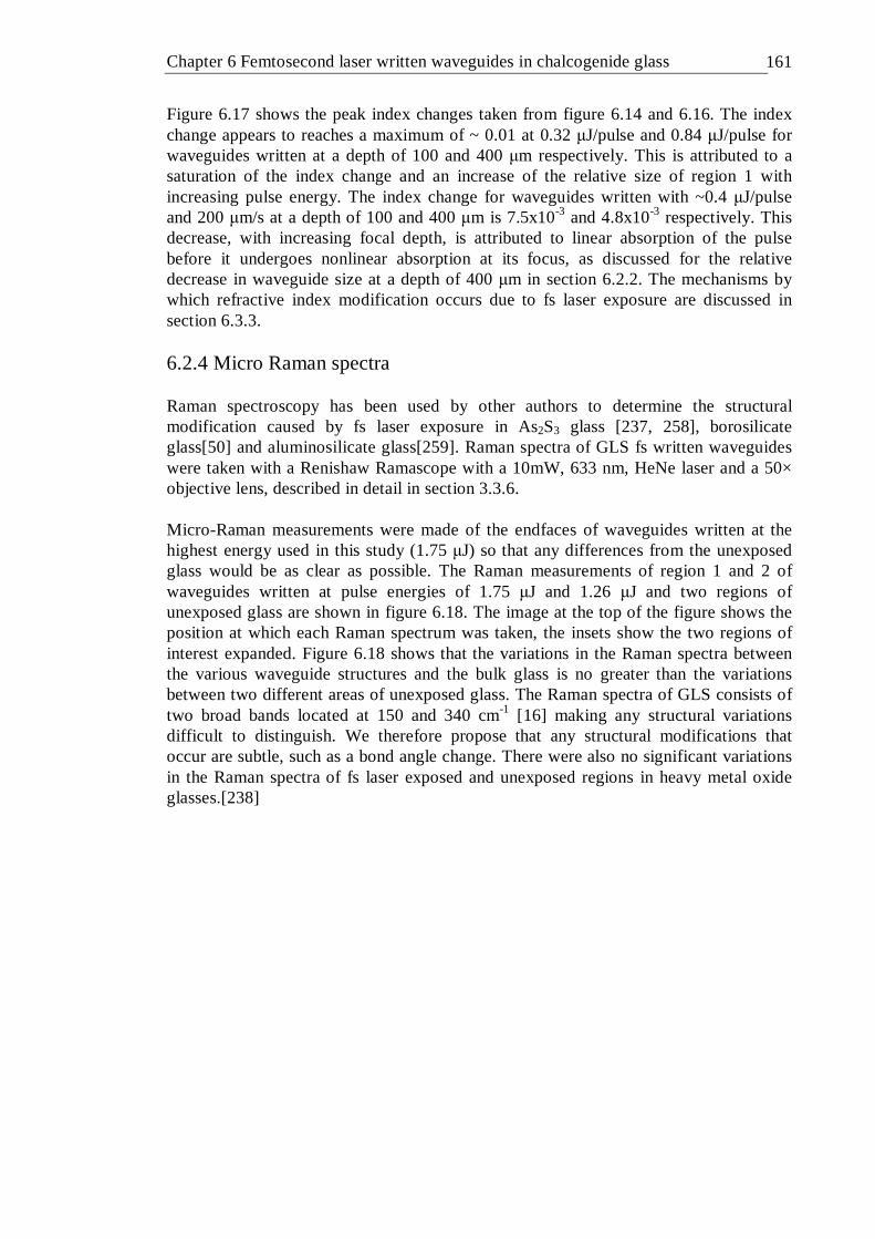
Chapter 6 Femtosecond laser written waveguides in chalcogenide glass 161
Figure 6.17 shows the peak index changes taken from figure 6.14 and 6.16. The index change appears to reaches a maximum of ~ 0.01 at 0.32 µJ/pulse and 0.84 µJ/pulse for waveguides written at a depth of 100 and 400 µm respectively. This is attributed to a saturation of the index change and an increase of the relative size of region 1 with increasing pulse energy. The index change for waveguides written with ~0.4 µJ/pulse and 200 µm/s at a depth of 100 and 400 µm is 7.5x10⁻³ and 4.8x10⁻³ respectively. This decrease, with increasing focal depth, is attributed to linear absorption of the pulse before it undergoes nonlinear absorption at its focus, as discussed for the relative decrease in waveguide size at a depth of 400 µm in section 6.2.2. The mechanisms by which refractive index modification occurs due to fs laser exposure are discussed in section 6.3.3. 6.2.4 Micro Raman spectra Raman spectroscopy has been used by other authors to determine the structural modification caused by fs laser exposure in As2S3 glass [237, 258], borosilicate glass[50] and aluminosilicate glass[259]. Raman spectra of GLS fs written waveguides were taken with a Renishaw Ramascope with a 10mW, 633 nm, HeNe laser and a 50× objective lens, described in detail in section 3.3.6. Micro-Raman measurements were made of the endfaces of waveguides written at the highest energy used in this study (1.75 µJ) so that any differences from the unexposed glass would be as clear as possible. The Raman measurements of region 1 and 2 of waveguides written at pulse energies of 1.75 µJ and 1.26 µJ and two regions of unexposed glass are shown in figure 6.18. The image at the top of the figure shows the position at which each Raman spectrum was taken, the insets show the two regions of interest expanded. Figure 6.18 shows that the variations in the Raman spectra between the various waveguide structures and the bulk glass is no greater than the variations between two different areas of unexposed glass. The Raman spectra of GLS consists of two broad bands located at 150 and 340 cm-1 [16] making any structural variations difficult to distinguish. We therefore propose that any structural modifications that occur are subtle, such as a bond angle change. There were also no significant variations in the Raman spectra of fs laser exposed and unexposed regions in heavy metal oxide glasses.[238]
Chapter 6 Femtosecond laser written waveguides in chalcogenide glass 162
Raman shift (cm-1)
200 400 600 800 1000 1200 1400 1600 1800
Inte
nsity
(A.U
.)
0.0
0.2
0.4
0.6
0.8
1.0
200 210 220 230 240 250 260 270 280
0.20
0.25
0.30
0.35
0.40
0.45
0.50
300 310 320 330 340 350 360 370
0.90
0.92
0.94
0.96
0.98
1.00
abcdef
a
b
c
d
e
f
FIGURE 6.18 Micro-Raman spectra of waveguides written at pulse energies of 1.75 µJ and 1.26 µJ and two regions of unexposed glass. The top image shows the position at which each Raman spectrum was taken.
Energy dispersive X-Ray (EDX) measurements of the region 1, region 2 and the unexposed glass found no compositional variation between these regions greater than the system detection limit of around 1%.

Chapter 6 Femtosecond laser written waveguides in chalcogenide glass 163
6.2.5 Waveguide transmission Waveguide transmission measurements are used here to examine the change in the absorption band-edge of the waveguides compared to bulk glass. This can be used to examine effects related to photo-darkening and colour centre formation. Waveguide transmission measurements were made using the setup shown in figure 6.5. The output from a tungsten halogen, white light source was attenuated with an iris and a neutral density filter before being collimated with two lenses and then modulated with a mechanical chopper. The collimated white light beam was then coupled into and out of the waveguides with a 10x microscope objectives. The guided modes were then imaged onto an iris and the selected guided mode was focused into a monochromator; the signal was then detected with a silicon detector using standard phase sensitive detection. In order to correct for the spectral dependence of the various optical components in the system a transmission measurement of the bulk glass (Isyst(λ)) was made. Then using the transmission measurement (Iref(λ)) of the same sample, measured using the Varian Cary 500 spectrophotometer, detailed in section 3.3.1, a correction spectrum (C(λ)) was calculated using equation 6.8.
)(
)()(
λλ
λsyst
ref
I
IC = (6.8)
FIGURE 6.19 Waveguide transmittance measurement setup.
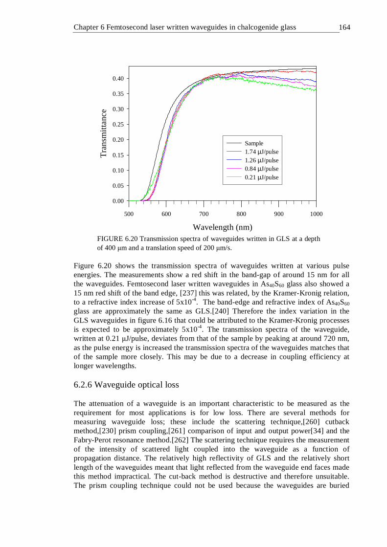
Chapter 6 Femtosecond laser written waveguides in chalcogenide glass 164
Wavelength (nm)
500 600 700 800 900 1000
Tra
nsm
itta
nce
0.00
0.05
0.10
0.15
0.20
0.25
0.30
0.35
0.40
Sample1.74 µJ/pulse1.26 µJ/pulse0.84 µJ/pulse0.21 µJ/pulse
FIGURE 6.20 Transmission spectra of waveguides written in GLS at a depth of 400 µm and a translation speed of 200 µm/s.
Figure 6.20 shows the transmission spectra of waveguides written at various pulse energies. The measurements show a red shift in the band-gap of around 15 nm for all the waveguides. Femtosecond laser written waveguides in As40S60 glass also showed a 15 nm red shift of the band edge, [237] this was related, by the Kramer-Kronig relation, to a refractive index increase of 5x10⁻⁴. The band-edge and refractive index of As40S60 glass are approximately the same as GLS.[240] Therefore the index variation in the GLS waveguides in figure 6.16 that could be attributed to the Kramer-Kronig processes is expected to be approximately 5x10⁻⁴. The transmission spectra of the waveguide, written at 0.21 µJ/pulse, deviates from that of the sample by peaking at around 720 nm, as the pulse energy is increased the transmission spectra of the waveguides matches that of the sample more closely. This may be due to a decrease in coupling efficiency at longer wavelengths. 6.2.6 Waveguide optical loss The attenuation of a waveguide is an important characteristic to be measured as the requirement for most applications is for low loss. There are several methods for measuring waveguide loss; these include the scattering technique,[260] cutback method,[230] prism coupling,[261] comparison of input and output power[34] and the Fabry-Perot resonance method.[262] The scattering technique requires the measurement of the intensity of scattered light coupled into the waveguide as a function of propagation distance. The relatively high reflectivity of GLS and the relatively short length of the waveguides meant that light reflected from the waveguide end faces made this method impractical. The cut-back method is destructive and therefore unsuitable. The prism coupling technique could not be used because the waveguides are buried

Chapter 6 Femtosecond laser written waveguides in chalcogenide glass 165
below the surface of the glass. The comparison of input and output power method requires the estimation of coupling efficiency, which could be prone to error because of the asymmetry of the waveguides. Waveguide loss measurements were therefore taken using the Fabry-Perot resonance method,[262] with the experimental setup shown in figure 6.21. By taking into account reflections from its end faces the waveguide structure may be regarded as a resonant cavity. By varying the wavelength of the input light source the output will reach periodic maxima (Imax) and minima (Imin), defining ζ= Imax/ Imin it can be shown[262] that the loss coefficient (α) of a waveguide can be calculated using equation 6.9.
+−−=
1
11ln
1
ξξα
RL (6.9)
Where R is the reflectivity of the end faces and L is the length of the waveguides. To carry out the experiment a fibre coupled Photonetics Tunics tuneable external cavity laser was coupled into and out of the waveguides with 10x 0.25 NA objectives with the output detected by a power meter. The guided mode of each waveguide was found with a CCD camera and any unguided radiation was blocked with an iris. The external cavity laser was scanned from 1550 to 1550.5 nm in steps of 0.001 nm and the waveguide output power plotted as a function of input wavelength. Error bounds were calculated from the variance of ζ and the accuracy to which R was known.
XYZ
10X
XYZXYZXYZ
10X10X
FIGURE 6.21 Waveguide loss measurements using the Fabry-Perot resonance method.
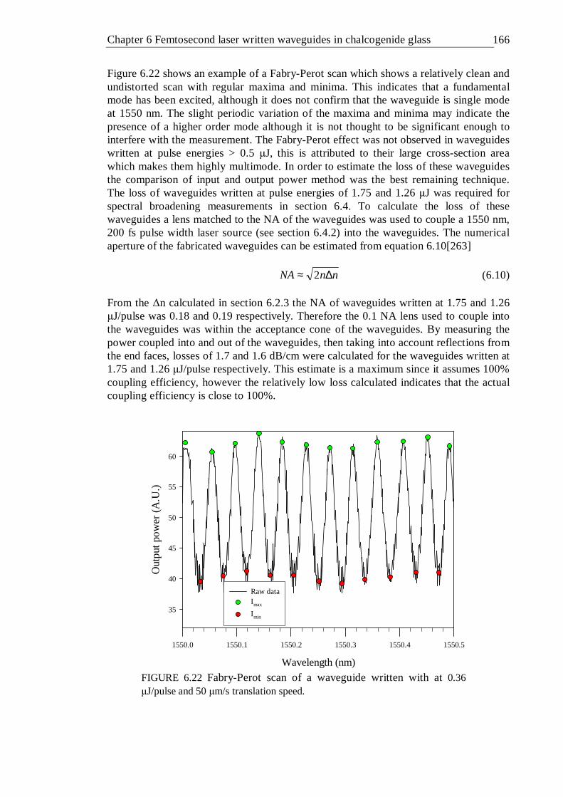
Chapter 6 Femtosecond laser written waveguides in chalcogenide glass 166
Figure 6.22 shows an example of a Fabry-Perot scan which shows a relatively clean and undistorted scan with regular maxima and minima. This indicates that a fundamental mode has been excited, although it does not confirm that the waveguide is single mode at 1550 nm. The slight periodic variation of the maxima and minima may indicate the presence of a higher order mode although it is not thought to be significant enough to interfere with the measurement. The Fabry-Perot effect was not observed in waveguides written at pulse energies > 0.5 µJ, this is attributed to their large cross-section area which makes them highly multimode. In order to estimate the loss of these waveguides the comparison of input and output power method was the best remaining technique. The loss of waveguides written at pulse energies of 1.75 and 1.26 µJ was required for spectral broadening measurements in section 6.4. To calculate the loss of these waveguides a lens matched to the NA of the waveguides was used to couple a 1550 nm, 200 fs pulse width laser source (see section 6.4.2) into the waveguides. The numerical aperture of the fabricated waveguides can be estimated from equation 6.10[263]
nnNA ∆≈ 2 (6.10) From the ∆n calculated in section 6.2.3 the NA of waveguides written at 1.75 and 1.26 µJ/pulse was 0.18 and 0.19 respectively. Therefore the 0.1 NA lens used to couple into the waveguides was within the acceptance cone of the waveguides. By measuring the power coupled into and out of the waveguides, then taking into account reflections from the end faces, losses of 1.7 and 1.6 dB/cm were calculated for the waveguides written at 1.75 and 1.26 µJ/pulse respectively. This estimate is a maximum since it assumes 100% coupling efficiency, however the relatively low loss calculated indicates that the actual coupling efficiency is close to 100%.
Wavelength (nm)
1550.0 1550.1 1550.2 1550.3 1550.4 1550.5
Out
put
po
wer
(A
.U.)
35
40
45
50
55
60
Raw dataImax
Imin
FIGURE 6.22 Fabry-Perot scan of a waveguide written with at 0.36 µJ/pulse and 50 µm/s translation speed.
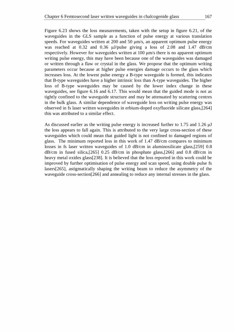
Chapter 6 Femtosecond laser written waveguides in chalcogenide glass 167
Figure 6.23 shows the loss measurements, taken with the setup in figure 6.21, of the waveguides in the GLS sample as a function of pulse energy at various translation speeds. For waveguides written at 200 and 50 µm/s, an apparent optimum pulse energy was reached at 0.32 and 0.36 µJ/pulse giving a loss of 2.08 and 1.47 dB/cm respectively. However for waveguides written at 100 µm/s there is no apparent optimum writing pulse energy, this may have been because one of the waveguides was damaged or written through a flaw or crystal in the glass. We propose that the optimum writing parameters occur because at higher pulse energies damage occurs to the glass which increases loss. At the lowest pulse energy a B-type waveguide is formed, this indicates that B-type waveguides have a higher intrinsic loss than A-type waveguides. The higher loss of B-type waveguides may be caused by the lower index change in these waveguides, see figure 6.16 and 6.17. This would mean that the guided mode is not as tightly confined to the waveguide structure and may be attenuated by scattering centres in the bulk glass. A similar dependence of waveguide loss on writing pulse energy was observed in fs laser written waveguides in erbium-doped oxyfluoride silicate glass,[264] this was attributed to a similar effect. As discussed earlier as the writing pulse energy is increased further to 1.75 and 1.26 µJ the loss appears to fall again. This is attributed to the very large cross-section of these waveguides which could mean that guided light is not confined to damaged regions of glass. The minimum reported loss in this work of 1.47 dB/cm compares to minimum losses in fs laser written waveguides of 1.0 dB/cm in aluminosilicate glass,[259] 0.8 dB/cm in fused silica,[265] 0.25 dB/cm in phosphate glass,[266] and 0.8 dB/cm in heavy metal oxides glass[238]. It is believed that the loss reported in this work could be improved by further optimisation of pulse energy and scan speed, using double pulse fs lasers[265], astigmatically shaping the writing beam to reduce the asymmetry of the waveguide cross-section[266] and annealing to reduce any internal stresses in the glass.
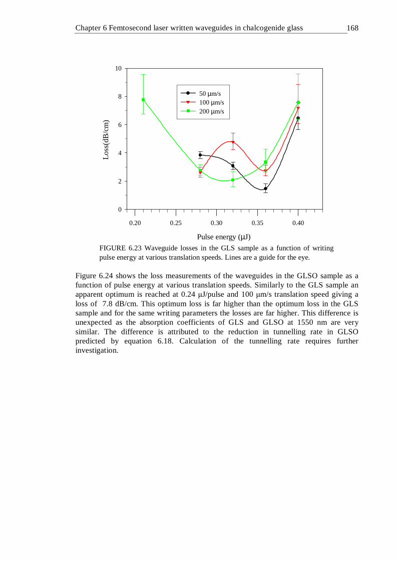
Chapter 6 Femtosecond laser written waveguides in chalcogenide glass 168
Pulse energy (µJ)
0.20 0.25 0.30 0.35 0.40
Loss
(dB
/cm
)
0
2
4
6
8
10
50 µm/s100 µm/s200 µm/s
FIGURE 6.23 Waveguide losses in the GLS sample as a function of writing pulse energy at various translation speeds. Lines are a guide for the eye.
Figure 6.24 shows the loss measurements of the waveguides in the GLSO sample as a function of pulse energy at various translation speeds. Similarly to the GLS sample an apparent optimum is reached at 0.24 µJ/pulse and 100 µm/s translation speed giving a loss of 7.8 dB/cm. This optimum loss is far higher than the optimum loss in the GLS sample and for the same writing parameters the losses are far higher. This difference is unexpected as the absorption coefficients of GLS and GLSO at 1550 nm are very similar. The difference is attributed to the reduction in tunnelling rate in GLSO predicted by equation 6.18. Calculation of the tunnelling rate requires further investigation.

Chapter 6 Femtosecond laser written waveguides in chalcogenide glass 169
Pulse energy (µJ)
0.10 0.15 0.20 0.25 0.30 0.35 0.40 0.45
Loss
(dB
/cm
)
6
8
10
12
14
20
25
200 µm/s100 µm/s
FIGURE 6.24 Waveguide losses in GLSO sample as a function of writing pulse energy at various translation speeds. Lines are a guide for the eye.
6.3 Discussion of waveguide formation mechanism In this section the observed waveguide structure and refractive index change profile presented in section 6.2.2 and 6.2.3 are discussed and analysed in terms of formation and non-linear absorption mechanisms. 6.3.1 Waveguide asymmetry The inherent asymmetry of the A-type waveguides could be explained as follows: perpendicular to the propagation direction (y axis) of the writing laser the waveguide dimension (Ly) is given approximately by the beam focal diameter 2ω0,
02ω≈yL (6.11)
while along the propagation direction (z axis) the waveguide dimension (Lz) is given by the confocal parameter b,
λπω 2
02=≈ bLz (6.12)
where ω0 is the focus waist. This results in a large difference in the waveguide sizes in the two directions.[266] Given that the focus waist of the 800 nm beam used to write the waveguides was around 1 µm, this corresponds to Ly ≈ 2 µm and Lz ≈ 8 µm. These dimensions do not correspond to either the A or B-type waveguides, however the aspect
Chapter 6 Femtosecond laser written waveguides in chalcogenide glass 170
ratio is similar to A-type waveguides and the dimensions are much closer (although still roughly half) to those of the central region of the A-type waveguides. Therefore further explanation of the waveguide structure is required. 6.3.2 Self focusing and plasma defocusing The phenomenon of self focusing, otherwise known as Kerr lensing, is a result of the intensity dependent non-linear refractive index given in equation 6.13[267]
Innn 20 += (6.13)
Where n0 is the linear refractive index, n2 is the non-linear refractive index and I is the laser irradiance. A Gaussian beam that is more intense at its centre than at its edges will experience a larger index change at its centre, so the beam effectively passes through a graded index lens which focuses the pulse. As the power of the laser pulse is increased further the self focusing becomes stronger until at some point it overcomes diffraction and the pulse undergoes a catastrophic collapse,[268] see figure 6.25(a). Given no other stabilisation mechanisms the beam is expected to form a singularity.[17, 269] However, in reality, as the pulse self focuses and the intensity rises it eventually becomes sufficient to non linearly ionize electrons producing an electron gas or plasma. This plasma contributes a negative refractive index change that prevents further self focusing.[18] The complex refractive index variation in the created plasma is quantitatively described by means of the laser induced plasma index modulation (∆npl) in equation 6.14[270]
+++−
=∆ ∫t
e
eee
e
epl dtEN
i
m
e
nn
0044
22332
0
)(exp1
)()1(2 ητω
ωττωτωω
τ(6.14)
Where τe is the free electron collision time, ω is the laser angular frequency, N0 is the initial plasma density, me is the electron mass, e is the electronic charge and η(E) is the probability per unit time for an electron to undergo an ionising collision. The realisation of the dynamic equilibrium between self focusing and plasma defocusing is a phenomenon known as filamentation. Filaments of light are robust light guides that are self confined without requiring a waveguide.
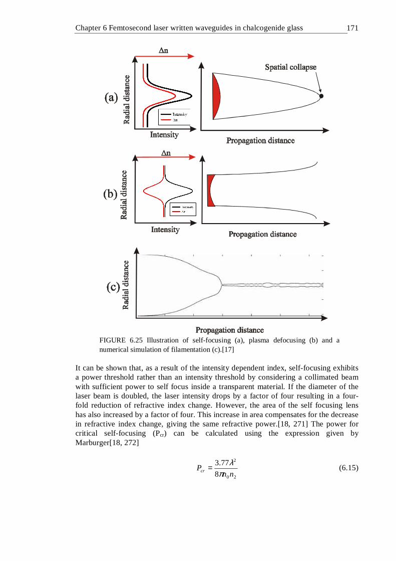
Chapter 6 Femtosecond laser written waveguides in chalcogenide glass 171
FIGURE 6.25 Illustration of self-focusing (a), plasma defocusing (b) and a numerical simulation of filamentation (c).[17]
It can be shown that, as a result of the intensity dependent index, self-focusing exhibits a power threshold rather than an intensity threshold by considering a collimated beam with sufficient power to self focus inside a transparent material. If the diameter of the laser beam is doubled, the laser intensity drops by a factor of four resulting in a four-fold reduction of refractive index change. However, the area of the self focusing lens has also increased by a factor of four. This increase in area compensates for the decrease in refractive index change, giving the same refractive power.[18, 271] The power for critical self-focusing (Pcr) can be calculated using the expression given by Marburger[18, 272]
20
2
8
77.3
nnPcr π
λ= (6.15)
Chapter 6 Femtosecond laser written waveguides in chalcogenide glass 172
GLS has n0 and n2 of 2.41 and 2.16x10⁻¹⁴ cm2/W respectively[240] which gives Pcr = 1.84 kW. This compares to Pcr = 1.5 MW calculated for borosilicate glass.[271] The irradiance required for the optical breakdown (Iob) of most dielectrics is around 1x10¹³ W/cm2.[238, 268] Assuming that Iob for GLS is comparable to that of other dielectrics, the relation Iob = Pcr/πω0
2 allows an estimation of the maximum focus waist acceptable to induce optical breakdown without critical self-focusing occurring, which gives a focus waist of 242 nm. This is much smaller than the actual focus waist inside the glass and indicates that the self focusing threshold is lower than the optical breakdown threshold. The inability to obtain material modification without self-focusing presents a problem for the formation of symmetric waveguides. The new beam waist produced by self-focusing is expected to be at a distance zf from the original focus point.[220]
cr
fPP
nz
/61.0
2 200
λω
= (6.16)
Where ω0 is the focus beam waist and P is the laser power. The lowest pulse energy used, 0.21 µJ, corresponds to a peak power of ~ 1.4 MW which in turn corresponds to zf of ~ 1 µm. This indicates that self focusing should cause little change in the position of the focus waist even at the lowest pulse energy. This is confirmed by the observation of no change in the focus waist position with varying pulse energy. In order to avoid self-focusing a longer wavelength could be used to increase the power for critical self-focusing, see equation 6.15. Because the threshold for optical breakdown depends on laser intensity and the threshold for self-focusing depends on laser power, tighter focusing of the beam may allow the intensity for optical breakdown to be reached before the critical power for self-focusing. However it is unclear whether non-linear absorption will occur at longer wavelengths and the high refractive index of GLS limits the focus waist that can be achieved. A possible way of avoiding the inherent asymmetry of waveguides, that happens when self focusing occurs would be to use parallel writing geometry. In parallel writing geometry the sample is translated in a direction parallel to the propagation direction of the writing laser beam. This method has been used to fabricate symmetric waveguides in aluminosilicate glass,[259] phosphate glass,[236] silicate and borosilicate glass.[50] This method is therefore proposed as further work. However, the length of the waveguides may be limited because of the linear absorption of the fs pulse that is believed to occur before it reached a focus, as discussed in section 6.2.1. Another method to fabricate symmetric waveguides could be to use two writing beams and form the waveguide from a densified region in-between the writing beams. 6.3.3 Refractive index change The physical origin of refractive index change produced in glass by fs laser exposure is not well understood. [50, 273] It is assumed that in the focal spot local rapid heating occurs. Heating the glass and freezing it while its temperature is still high could produce a lowering of the refractive index.[50] Is has been proposed that the plasma induced by a fs pulse in glass expands rapidly, creating a shock wave or micro-explosion.[274] This shockwave could compress the glass and increase the refractive index.

Chapter 6 Femtosecond laser written waveguides in chalcogenide glass 173
A rapid quenching model has been proposed to explain index modification in glasses after fs laser exposure.[275] This model assumes that, after a high temperature plasma is formed by the laser pulse it cools rapidly, freezing the glass in the same structure that it had at high temperature. The temperature at which a glass structure becomes frozen is called the fictive temperature (Tf). The concept of fictive temperature was proposed by Tool[276] who suggested that, depending on the cooling rate, glass has a frozen in structure that corresponds to some temperature (the fictive temperature) of an equilibrium liquid.[277] In silica glass fs laser exposure induces a positive index change [50, 263] which is explained by the rapid quenching model as rapidly quenched silica is known to have a positive index change.[41, 277] In phosphate glass, fs laser exposure induces a negative index change[236] which is explained by the rapid quenching model because rapidly quenched phosphate glass is known to have a negative index change.[236] Negative index change after fs laser exposure has also been observed in borosilicate, heavy metal oxide and lanthanum-borate glasses.[273] The dependence of refractive index on fictive temperature has not been measured in GLS. However, since measurements in section 6.2.3 indicate that fs exposure of GLS can result in a negative index change it is proposed that the refractive index of GLS has a negative dependence on fictive temperature; in other words the higher the temperature GLS is rapidly quenched from, the lower the resulting refractive index will be. Also according to the Lorenz-Lorentz relationship, compaction increases and expansion decreases the refractive index of glasses.[278, 279] Other authors have suggested a colour centre model to explain index modification in glasses after fs laser exposure.[50, 221, 280] This model stipulates that fs laser pulses introduce defects called colour centres in sufficient numbers and strength to alter the index through a Kramers-Kronig mechanism. Waveguide transmission measurements, see section 6.2.5, indicate that the maximum index change due to a Kramers-Kronig mechanism in fs laser written GLS waveguides is ~ 5x10⁻⁴ which is a factor of 20 smaller than the index change measured by QPM in section 6.2.3. This indicates that colour centre formation does not play a significant roll in the index modification of fs laser written GLS waveguides. Positive index change resulting from densification has been attributed to many fs laser written waveguides in glasses[238, 273, 280, 281]. Laser induced compaction of GLS glass has been shown to result in a positive index change,[282] which has been related to the rather open three-dimensional structure of GLS that can be rearranged to a more compact structure by laser exposure.[278] Based on the above discussion it is proposed that the negative index change of region 1 in A-type waveguides is the result of it having a high fictive temperature; the positive index change of region 2 in A-type waveguides is the result of densification. Because of the lower intensity used in their formation, the positive index change in B-type waveguides may simply be analogous to the positive index change observed in CW, UV written waveguides in GLS.[282]

Chapter 6 Femtosecond laser written waveguides in chalcogenide glass 174
The maximum observed index change of ~ 0.01 in fs laser written waveguides in GLS (this work) compares to 0.08 in As2S3 glass[258], 3.5x10⁻³ in silica glass [50] and 4x10⁻³ in borosilicate glass[50] 6.3.4 Waveguide formation mechanism The form and structure of B-type waveguides indicates that they are formed by filamentation. However, as the pulse energy is increased and type-A waveguides are formed filamentation is no longer observed. This indicates that there is a threshold at the transition between the formation of B-type and A-type waveguides (EBA) where a large increase in plasma density breaks the equilibrium between self focusing and plasma defocusing; EBA is estimated to be around 0.2 µJ/pulse. This indicates, along with the guided mode and reflection optical micrograph findings in section 6.2.2 and the discussion of index modification in section 6.2.3, that the A-type waveguide structure is formed by a similar mechanism that occurs in phosphate glass[236] and sodium calcium silicate glass[275]. In these glasses the fs laser beam induces a modified region in its focal volume that has a lower density and refractive index than the initial glass; this exposed region did not guide light and it was only regions peripheral to the exposed region that guided light. It is therefore proposed that region 1 was formed by exposure to the focused fs laser beam where a high density plasma was formed. The waveguide structure that actively guides light (region 2) was formed by movement of glass from the fs laser exposed region in a shock wave that resulted in a region of higher density and higher refractive index. The B-type waveguide structure was formed through filamentation and the plasma density was not high enough to induce a negative refractive index change. These mechanisms for the formation of A-type and B-type waveguides are illustrated in figure 6.26.
-∆ ∆n/n,+ v/v(region 1)
+ n/n,- v/v(region 2)∆ ∆
+ n/n,- v/v∆ ∆
A-type B-type
FIGURE 6.26 Waveguide formation mechanism in GLS at pulse energies > ~0.2 µJ/pulse (A-type) and GLS at pulse energies < ~0.2 µJ/pulse (B-type).

Chapter 6 Femtosecond laser written waveguides in chalcogenide glass 175
6.3.5 Non-linear absorption Several mechanisms for nonlinear absorption of fs pulses have been considered in the literature; the principal ones are multiphoton ionisation (MPI), tunnelling and avalanche ionisation.
FIGURE 6.27 Schematic diagram of the photoionisation of an electron in a Coulomb well for different values of the Keldysh parameter leading to tunnelling (a), an intermediate scheme (b) and multi-photon ionisation (c); after [18].
In tunnelling ionisation, the high electric field of the laser pulse deforms the Coulomb well that binds a valence electron to its parent atom. If the electric field is strong enough the Coulomb well can be deformed enough that the bound electron tunnels through the short barrier and becomes free, as shown in figure 6.27(a). In a solid the electron is promoted from the valence to the conduction band, rather than ionised.[18] In multi-photon ionisation (MPI), shown in figure 6.27(c) a valence electron is promoted to the conduction band via the simultaneous absorption of several photons having satisfied the condition that the number of photons absorbed (m) times the photon energy is equal to or greater than the band-gap of the material.[18] In the intermediate case tunnelling and MPI occur simultaneously, as shown in figure 6.27(b). The ionisation rate in the multi-photon ionisation regime (WMPI) is given by equation 6.17[50]
mmMPI IW σ= (6.17)
Where σm is the multi-photon absorption coefficient for absorption of m photons and I is the laser intensity. The ionisation rate in the tunnelling regime is given by equation 6.18[283]
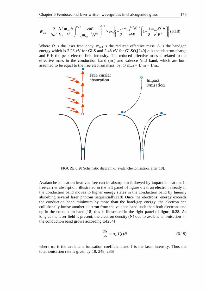
Chapter 6 Femtosecond laser written waveguides in chalcogenide glass 176
∆Ω−∆−×
∆
∆∆=22
22/32/12/5
9/32/1
2/3
22 8
11
2exp
9
2
Ee
m
Ee
m
m
EemW redred
red
redtun
h
h
hh
ππ
(6.18)
Where Ω is the laser frequency, mred is the reduced effective mass, ∆ is the bandgap energy which is 2.28 eV for GLS and 2.48 eV for GLSO,[240] e is the electron charge and E is the peak electric field intensity. The reduced effective mass is related to the effective mass in the conduction band (mc) and valence (mv) band, which are both assumed to be equal to the free electron mass, by: 1/ mred = 1/ mc+ 1/mv.
FIGURE 6.28 Schematic diagram of avalanche ionisation, after[18]. Avalanche ionisation involves free carrier absorption followed by impact ionisation. In free carrier absorption, illustrated in the left panel of figure 6.28, an electron already in the conduction band moves to higher energy states in the conduction band by linearly absorbing several laser photons sequentially.[18] Once the electrons’ energy exceeds the conduction band minimum by more than the band-gap energy, the electron can collisionally ionise another electron from the valence band such than both electrons end up in the conduction band;[18] this is illustrated in the right panel of figure 6.28. As long as the laser field is present, the electron density (N) due to avalanche ionisation in the conduction band grows according to[284]
NtIdt
dNai )(α= (6.19)
where αai is the avalanche ionisation coefficient and I is the laser intensity. Thus the total ionisation rate is given by[18, 248, 285]
Chapter 6 Femtosecond laser written waveguides in chalcogenide glass 177
LossPI WNtIIWdt
dN −+∆Ω= )(),,( α (6.20)
Where WPI is the photoionisation rate, generalised for either multi photon absorption or tunnelling, and WLoss is the loss rate due to electron diffusion and recombination. It has been proposed by several authors that avalanche ionisation is of little importance in the absorption of sub-picosecond pulses in transparent materials.[50, 285, 286] However, other authors have proposed that it does[18, 284]. Therefore, in the absence of another explanation, it is proposed that the expected rapid increase in plasma density that breaks down the dynamic equilibrium between self focusing and plasma defocusing (discussed in section 6.3.2) and causes a transition from A-type to B-type waveguides is instigated by avalanche ionisation. In order to determine whether MPI or tunnelling dominate the nonlinear absorption the Keldysh parameter (γ) can be calculated using equation 6.21.[50, 283, 286, 287]
eE
mred∆Ω=γ (6.21)
For γ>1 MPI is dominant, for γ < 1 tunnelling is dominant. The waveguides investigated in this study were written with pulse energies of 0.21 to 1.74 µJ which corresponds to a Keldysh parameter (γ) of 0.11 to 0.04; this indicates that tunnelling was the dominant nonlinear absorption process in the formation of all the waveguides investigated in this study.
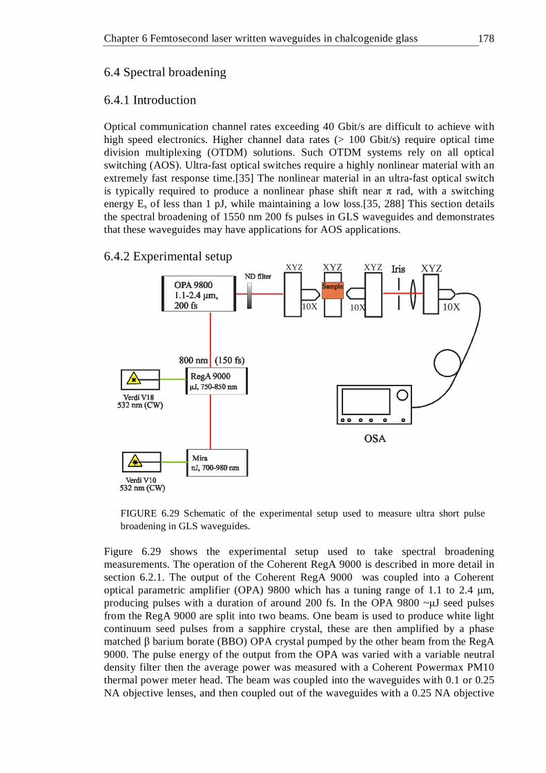
Chapter 6 Femtosecond laser written waveguides in chalcogenide glass 178
6.4 Spectral broadening 6.4.1 Introduction Optical communication channel rates exceeding 40 Gbit/s are difficult to achieve with high speed electronics. Higher channel data rates (> 100 Gbit/s) require optical time division multiplexing (OTDM) solutions. Such OTDM systems rely on all optical switching (AOS). Ultra-fast optical switches require a highly nonlinear material with an extremely fast response time.[35] The nonlinear material in an ultra-fast optical switch is typically required to produce a nonlinear phase shift near π rad, with a switching energy Es of less than 1 pJ, while maintaining a low loss.[35, 288] This section details the spectral broadening of 1550 nm 200 fs pulses in GLS waveguides and demonstrates that these waveguides may have applications for AOS applications. 6.4.2 Experimental setup
XYZ
10X
XYZXYZXYZ
10X10X
FIGURE 6.29 Schematic of the experimental setup used to measure ultra short pulse broadening in GLS waveguides.
Figure 6.29 shows the experimental setup used to take spectral broadening measurements. The operation of the Coherent RegA 9000 is described in more detail in section 6.2.1. The output of the Coherent RegA 9000 was coupled into a Coherent optical parametric amplifier (OPA) 9800 which has a tuning range of 1.1 to 2.4 µm, producing pulses with a duration of around 200 fs. In the OPA 9800 ~µJ seed pulses from the RegA 9000 are split into two beams. One beam is used to produce white light continuum seed pulses from a sapphire crystal, these are then amplified by a phase matched β barium borate (BBO) OPA crystal pumped by the other beam from the RegA 9000. The pulse energy of the output from the OPA was varied with a variable neutral density filter then the average power was measured with a Coherent Powermax PM10 thermal power meter head. The beam was coupled into the waveguides with 0.1 or 0.25 NA objective lenses, and then coupled out of the waveguides with a 0.25 NA objective

Chapter 6 Femtosecond laser written waveguides in chalcogenide glass 179
lens. The guided modes were isolated with an iris then coupled into a single mode silica fibre with a 0.1 NA lens and a 0.25 NA objective lens. The beam was then detected with an Ando AQ6315A optical spectrum analyser (OSA) which had a detection range of 350 to 1750 nm and was set to a resolution of 5 nm. Measurement of the beams’ average power before it was coupled into the waveguides, i.e. the power incident on the waveguide (Pinc), was found not to accurately represent the power coupled into the waveguides. This is because the NA, cross section area and asymmetry of the various waveguides examined varied, this in turn varied the coupling efficiency of the waveguides considerably. Therefore it was decided to measure the output power from the waveguides (Pout). The power coupled into the waveguides (Pin) was estimated from Pout by taking into account reflections from the waveguide’s output end face and the loss of the waveguide. The waveguide losses are calculated in section 6.2.6. Since the beam shifted in wavelength and broadened after passing through the waveguides it was decided to calculate the output power from the waveguide output spectra Iout(λ) from the OSA. This is because the available power meters required calibration to one particular wavelength and they had a lower sensitivity than the OSA. Pout was calculated from the ratio of the number of photons in Iout(λ) to the number of photons in a spectrum of the laser beam that had not passed through the waveguides (I ref(λ)) which had a power measured with a thermal power meter (Pref). The number of photons (n) detected at a particular wavelength is proportional to the measured irradiance I(λ) multiplied by the wavelength (λ), therefore Pout was calculated with equation 6.22.
∫∫=
λλλ
λλλ
dI
dIPP
ref
out
refout)(
)( (6.22)
As illustrated in figure 6.30 Pout was found to be a very nearly a linear function of Pinc, indicating that no two photon absorption was occurring. Taking into account the reflectivity (R) of GLS, which was 0.1632, and the propagation loss of the waveguides (Γ), Pin was calculated using equation 6.23.
R
PP out
in −Γ
=1
(6.23)
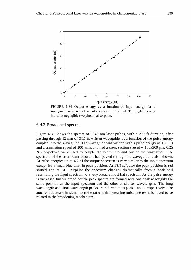
Chapter 6 Femtosecond laser written waveguides in chalcogenide glass 180
Input energy (nJ)
0 20 40 60 80 100 120 140 160
Out
put
ene
rgy
(nJ)
0
20
40
60
80
100
FIGURE 6.30 Output energy as a function of input energy for a waveguide written with a pulse energy of 1.26 µJ. The high linearity indicates negligible two photon absorption.
6.4.3 Broadened spectra Figure 6.31 shows the spectra of 1540 nm laser pulses, with a 200 fs duration, after passing through 12 mm of GLS fs written waveguide, as a function of the pulse energy coupled into the waveguide. The waveguide was written with a pulse energy of 1.75 µJ and a translation speed of 200 µm/s and had a cross section size of ~ 100x300 µm, 0.25 NA objectives were used to couple the beam into and out of the waveguide. The spectrum of the laser beam before it had passed through the waveguide is also shown. At pulse energies up to 4.7 nJ the output spectrum is very similar to the input spectrum except for a small blue shift in peak position. At 18.8 nJ/pulse the peak position is red shifted and at 31.3 nJ/pulse the spectrum changes dramatically from a peak still resembling the input spectrum to a very broad almost flat spectrum. As the pulse energy is increased further broad double peak spectra are formed with one peak at roughly the same position as the input spectrum and the other at shorter wavelengths. The long wavelength and short wavelength peaks are referred to as peak 1 and 2 respectively. The apparent decrease in signal to noise ratio with increasing pulse energy is believed to be related to the broadening mechanism.
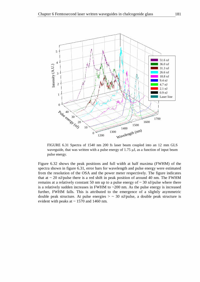
Chapter 6 Femtosecond laser written waveguides in chalcogenide glass 181
0
1
2
3
4
5
12001300
14001500
16001700
0
10
20
30
40
Inte
nsity
(A
.U.)
Wavelength (nm)
Pulse energy (nJ)
51.6 nJ36.0 nJ31.3 nJ26.6 nJ18.8 nJ9.4 nJ4.7 nJ2.1 nJ0.9 nJLaser line
FIGURE 6.31 Spectra of 1540 nm 200 fs laser beam coupled into an 12 mm GLS waveguide, that was written with a pulse energy of 1.75 µJ, as a function of input beam pulse energy.
Figure 6.32 shows the peak positions and full width at half maxima (FWHM) of the spectra shown in figure 6.31, error bars for wavelength and pulse energy were estimated from the resolution of the OSA and the power meter respectively. The figure indicates that at ~ 20 nJ/pulse there is a red shift in peak position of around 40 nm. The FWHM remains at a relatively constant 50 nm up to a pulse energy of ~ 30 nJ/pulse where there is a relatively sudden increases in FWHM to ~200 nm. As the pulse energy is increased further, FWHM falls. This is attributed to the emergence of a slightly asymmetric double peak structure. At pulse energies > ~ 30 nJ/pulse, a double peak structure is evident with peaks at ~ 1570 and 1460 nm.
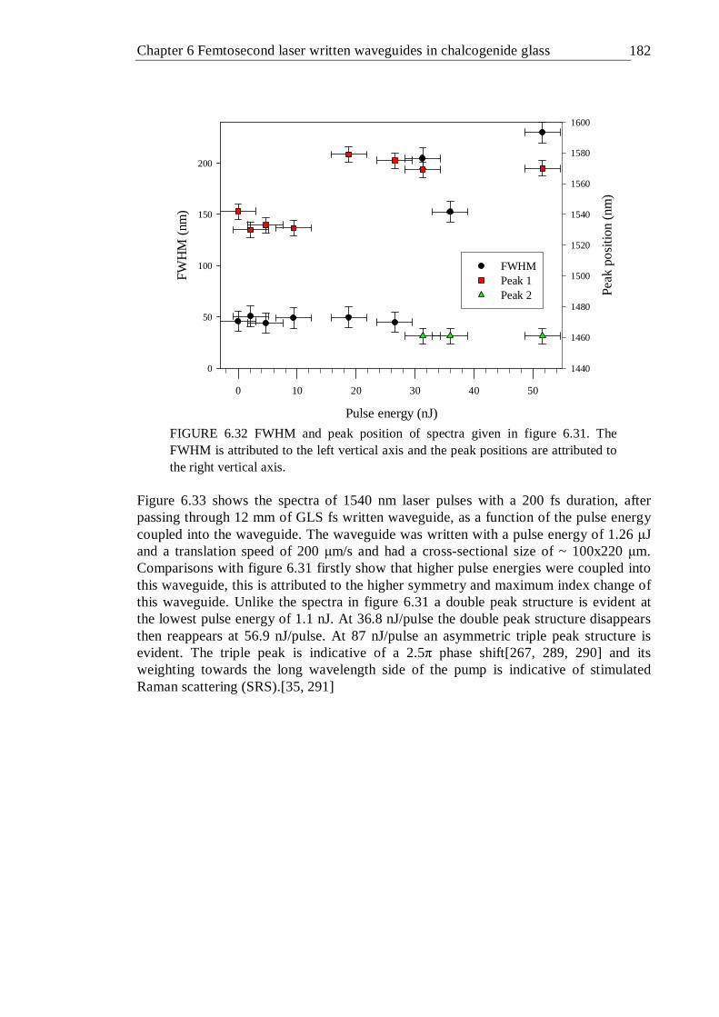
Chapter 6 Femtosecond laser written waveguides in chalcogenide glass 182
Pulse energy (nJ)
0 10 20 30 40 50
FW
HM
(nm
)
0
50
100
150
200
Pe
ak
posi
tion
(nm
)
1440
1460
1480
1500
1520
1540
1560
1580
1600
FWHMPeak 1Peak 2
FIGURE 6.32 FWHM and peak position of spectra given in figure 6.31. The FWHM is attributed to the left vertical axis and the peak positions are attributed to the right vertical axis.
Figure 6.33 shows the spectra of 1540 nm laser pulses with a 200 fs duration, after passing through 12 mm of GLS fs written waveguide, as a function of the pulse energy coupled into the waveguide. The waveguide was written with a pulse energy of 1.26 µJ and a translation speed of 200 µm/s and had a cross-sectional size of ~ 100x220 µm. Comparisons with figure 6.31 firstly show that higher pulse energies were coupled into this waveguide, this is attributed to the higher symmetry and maximum index change of this waveguide. Unlike the spectra in figure 6.31 a double peak structure is evident at the lowest pulse energy of 1.1 nJ. At 36.8 nJ/pulse the double peak structure disappears then reappears at 56.9 nJ/pulse. At 87 nJ/pulse an asymmetric triple peak structure is evident. The triple peak is indicative of a 2.5π phase shift[267, 289, 290] and its weighting towards the long wavelength side of the pump is indicative of stimulated Raman scattering (SRS).[35, 291]
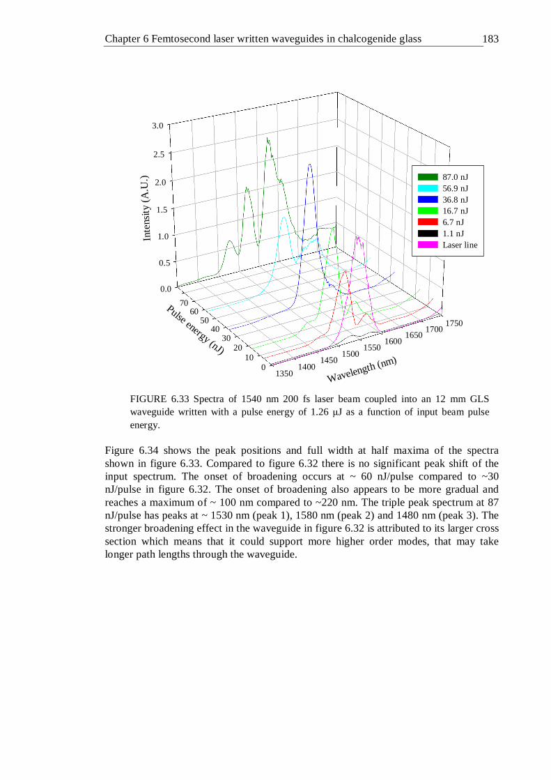
Chapter 6 Femtosecond laser written waveguides in chalcogenide glass 183
0.0
0.5
1.0
1.5
2.0
2.5
3.0
13501400
14501500
15501600
16501700
1750
010
2030
4050
6070
Inte
nsity
(A
.U.)
Wavelength (nm)
Pulse energy (nJ)
87.0 nJ56.9 nJ36.8 nJ16.7 nJ6.7 nJ1.1 nJLaser line
FIGURE 6.33 Spectra of 1540 nm 200 fs laser beam coupled into an 12 mm GLS waveguide written with a pulse energy of 1.26 µJ as a function of input beam pulse energy.
Figure 6.34 shows the peak positions and full width at half maxima of the spectra shown in figure 6.33. Compared to figure 6.32 there is no significant peak shift of the input spectrum. The onset of broadening occurs at ~ 60 nJ/pulse compared to ~30 nJ/pulse in figure 6.32. The onset of broadening also appears to be more gradual and reaches a maximum of ~ 100 nm compared to ~220 nm. The triple peak spectrum at 87 nJ/pulse has peaks at ~ 1530 nm (peak 1), 1580 nm (peak 2) and 1480 nm (peak 3). The stronger broadening effect in the waveguide in figure 6.32 is attributed to its larger cross section which means that it could support more higher order modes, that may take longer path lengths through the waveguide.
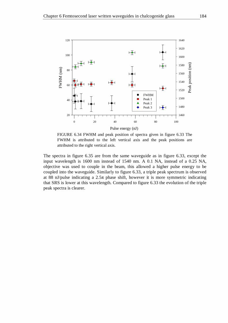
Chapter 6 Femtosecond laser written waveguides in chalcogenide glass 184
Pulse energy (nJ)
0 20 40 60 80 100
FW
HM
(nm
)
20
40
60
80
100
120
Pe
ak
pos
ition
(nm
)
1460
1480
1500
1520
1540
1560
1580
1600
1620
1640
FWHM Peak 1 Peak 2 Peak 3
FIGURE 6.34 FWHM and peak position of spectra given in figure 6.33 The FWHM is attributed to the left vertical axis and the peak positions are attributed to the right vertical axis.
The spectra in figure 6.35 are from the same waveguide as in figure 6.33, except the input wavelength is 1600 nm instead of 1540 nm. A 0.1 NA, instead of a 0.25 NA, objective was used to couple in the beam, this allowed a higher pulse energy to be coupled into the waveguide. Similarly to figure 6.33, a triple peak spectrum is observed at 88 nJ/pulse indicating a 2.5π phase shift, however it is more symmetric indicating that SRS is lower at this wavelength. Compared to figure 6.33 the evolution of the triple peak spectra is clearer.
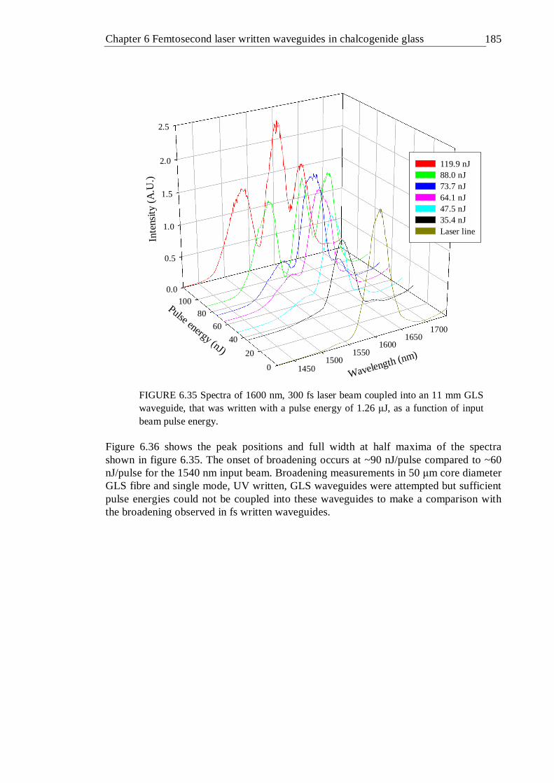
Chapter 6 Femtosecond laser written waveguides in chalcogenide glass 185
0.0
0.5
1.0
1.5
2.0
2.5
14501500
15501600
16501700
0
20
40
60
80
100
Inte
nsity
(A
.U.)
Wavelength (nm)
Pulse energy (nJ)
119.9 nJ88.0 nJ73.7 nJ64.1 nJ47.5 nJ35.4 nJLaser line
FIGURE 6.35 Spectra of 1600 nm, 300 fs laser beam coupled into an 11 mm GLS waveguide, that was written with a pulse energy of 1.26 µJ, as a function of input beam pulse energy.
Figure 6.36 shows the peak positions and full width at half maxima of the spectra shown in figure 6.35. The onset of broadening occurs at ~90 nJ/pulse compared to ~60 nJ/pulse for the 1540 nm input beam. Broadening measurements in 50 µm core diameter GLS fibre and single mode, UV written, GLS waveguides were attempted but sufficient pulse energies could not be coupled into these waveguides to make a comparison with the broadening observed in fs written waveguides.
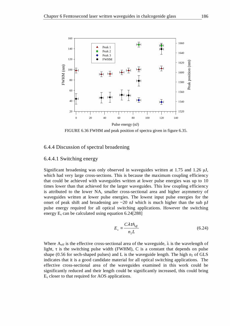
Chapter 6 Femtosecond laser written waveguides in chalcogenide glass 186
Pulse energy (nJ)
0 20 40 60 80 100 120 140
Pe
ak p
ositi
on
(nm
)
1520
1540
1560
1580
1600
1620
1640
1660
FW
HM
(nm
)
20
40
60
80
100
120
140
160
Peak 1 Peak 2 Peak 3 FWHM
FIGURE 6.36 FWHM and peak position of spectra given in figure 6.35.
6.4.4 Discussion of spectral broadening 6.4.4.1 Switching energy Significant broadening was only observed in waveguides written at 1.75 and 1.26 µJ, which had very large cross-sections. This is because the maximum coupling efficiency that could be achieved with waveguides written at lower pulse energies was up to 10 times lower than that achieved for the larger waveguides. This low coupling efficiency is attributed to the lower NA, smaller cross-sectional area and higher asymmetry of waveguides written at lower pulse energies. The lowest input pulse energies for the onset of peak shift and broadening are ~20 nJ which is much higher than the sub pJ pulse energy required for all optical switching applications. However the switching energy Es can be calculated using equation 6.24[288]
Ln
ACE eff
s2
λτ= (6.24)
Where Aeff is the effective cross-sectional area of the waveguide, λ is the wavelength of light, τ is the switching pulse width (FWHM), C is a constant that depends on pulse shape (0.56 for sech-shaped pulses) and L is the waveguide length. The high n2 of GLS indicates that it is a good candidate material for all optical switching applications. The effective cross-sectional area of the waveguides examined in this work could be significantly reduced and their length could be significantly increased, this could bring Es closer to that required for AOS applications.
Chapter 6 Femtosecond laser written waveguides in chalcogenide glass 187
6.4.4.2 Self phase modulation Self phase modulation (SPM) is a manifestation of the intensity dependence of the refractive index in nonlinear media and leads to the spectral broadening of optical pulses.[267] SPM is the temporal analogue of self focusing (see section 6.3.2). SPM causes a phase shift between the peak of an optical pulse and its low intensity leading and trailing edges, resulting in the spectral broadening of the pulse. The nonlinear phase shift induced by SPM is given by[243]
mod
022
A
PnLeffSPM λ
πφ = (6.25)
Where P0 is the peak pulse power, n2 is the nonlinear refractive index, Amod is the effective mode area and Leff is the effective length, defined as
α
αL
eff
eL
−−= 1 (6.26)
Where α is the loss coefficient and L is the waveguide length. For the maximum pulse energy of ~ 100nJ, used in figure 6.35, and approximating Amod to the cross-sectional area of the waveguide, the phase shift calculated using equation 6.25 is ~π. However, the value of Amod may be an overestimate because the guided mode is confined to certain regions of the waveguide therefore the phase shift calculated using equation 6.25 may be an underestimate. The number of peaks and the extent of the broadening in an SPM broadened spectrum are dependent on the magnitude of the nonlinear phase shift and increase with it linearly.[243] The oscillatory structure of the broadened pulses in figures 6.31, 6.33 and 6.35 are indicative of SPM. The maximum phase shift Φmax of an SPM broadened pulse is given approximately by [267, 289]
πφ
−≈2
1max M (6.27)
Where M is the number of peaks in an SPM broadened spectrum. Equation 6.27 and a comparison with other SPM broadened spectra[267, 290] indicate that the double peak structure in figure 6.31 demonstrates a 1.5π phase shift, at 36 nJ/pulse, and the triple peak structure in figure 6.33 and 6.35 demonstrates a 2.5π phase shift, at 87 and 88 nJ/pulse respectively. These nonlinear phase shifts compare to a maximum phase shift of 1.6π and 3.5π in 2.03 cm[288] and 2.8 cm[35] long photodarkened planar Ge0.25Se0.75 glass waveguides respectively. The spectral bandwidth of pulses broadened by SPM (∆ωSPM) is given by[246]
effSPM A
LPn
λπωω 020 2∆
=∆ (6.28)

Chapter 6 Femtosecond laser written waveguides in chalcogenide glass 188
Where ∆ω0 is the bandwidth of the input pulse. For the maximum pulse energy of 50 nJ, used in figure 6.31, the bandwidth for pulses broadened by SPM is ~100 nm, however the observed bandwidth of the broadened pulse was ~ 200 nm. This extra broadening is attributed to stimulated Raman scattering. For pulse widths < 100 ps the combined effect of group velocity dispersion (GVD) and SPM can become significant.[267] GVD causes a short pulse of light to spread in time as a result of different frequency components of the pulse traveling at different velocities.[267] An effect of the interplay between GDV and SPM on the pulse spectrum is to reduce the depth of the minima that would be expected in a pulse spectrum broadened by SPM alone.[267] This is evident in the spectra in figure 6.31, but not in figure 6.33 and 6.35. A measurement of the pulse width after passing through the waveguides would provide more information on the effect of GVD, however this measurement requires an autocorrelator which was not available at the time. Therefore pulse-width measurement is suggested as further work. 6.4.4.3 Stimulated Raman scattering Stimulated Raman scattering (SRS) is an important nonlinear process that can be exploited to construct broadband fibre based Raman amplifiers and tuneable Raman lasers.[243] At low intensities, spontaneous Raman scattering can transfer a small fraction (typically ~10-6) of power from one optical field to another, whose frequency is downshifted by an amount determined by the vibration modes of the medium.[267] The downshifted radiation is called the Stokes wave. The spontaneous Raman effect is also discussed in section 3.3.6. At high pump intensities the nonlinear phenomenon of SRS can occur in which the Stokes wave grows rapidly inside the medium such that most of the pump energy is transferred to it.[267] The SRS generated Stokes wave intensity Is for a CW, or quasi CW, condition is given by[243]
))0(exp()0()( LLIgILI seffprss α−= ,p
L
eff
peL
α
α−−= 1 (6.29)
Where L is the waveguide length, Is(0) is the Stokes intensity at L=0, αs and αp are the waveguides’ loss coefficients at the Stokes and pump wavelengths respectively, Leff is the effective length, defined by αp, and gr is the Raman gain coefficient. In general gr
depends on composition and dopants in the waveguide material and is inversely proportional to pump wavelength.[243] For pulses with widths below 100 ps, the length of the waveguide can exceed the walk-off length, Lw, defined as[267]
11
0
−− −=
gsgp
wvv
TL (6.30)
Where vgp and vgs are the group velocities of the pump and Stokes pulses respectively and T0 is the duration of the pump pulse. The Raman threshold is defined as the pump power at which the Stokes power becomes equal to the pump power at the waveguide output. Assuming a Lorentzian shape for the
Chapter 6 Femtosecond laser written waveguides in chalcogenide glass 189
Raman gain spectrum and a CW or quasi CW condition, the critical power Pcr required to reach the Raman threshold, to a good approximation, is given by.[292]
effrcr Lg
AP mod16
≈ (6.31)
For the short pulse condition, equation 6.31 holds provided the effective length is taken to be: Leff = √πLw.[267] In silica fibre the SPM broadened pump spectra became broadened with an asymmetry weighted towards the long wavelength end of the pump spectrum once the pump power passes the Raman threshold. This is similar to the effect observed at the highest pulse energy in figure 6.33. It is therefore proposed that the asymmetry of the triple peak structure in figure 6.33 when the input beam was 1540 nm is cause by the peak power exceeding the Raman threshold. The higher symmetry of the SPM broadened triple peak structure, in figure 6.35, when the input beam was 1600 nm indicates that the Raman threshold was not reached in this case. This can be explained by examining equation 6.31 and considering that gr is inversely proportional to input beam wavelength, therefore at longer input beam wavelengths the Raman threshold will be higher. 6.4.4.4 Device applications Two of the nonlinear optical devices, mentioned in section 6.1.3, are considered here as possible applications of the pulse broadening effect discussed in this section. Because the birefringent properties of the waveguides have not been studied, optical Kerr shutters are not discussed here. The different broadening behaviours observed for waveguides written at different pulse energies indicate that waveguide writing parameters could be used to customise the broadening properties of a waveguide for a specific application. The fabrication of passive optical components such as Fresnel zone plates and fibre attenuators, as mentioned in section 6.1.2, has been demonstrated in silica but not in a highly nonlinear glass such as GLS, this is therefore suggested as further work. The methods of waveguide fabrication presented in this chapter, could be used to construct a ring resonator[293] which could have applications as optical filters[294] and all optical switching devices.[295] This is therefore suggested as further work. 6.4.4.5 Mach-Zehnder interferometer switch The operation of these devices is described in section 6.1.3.1; as discussed here a π phase shift is required for the operation of these devices. Calculations, in section 6.4.4.2, indicate that a 2.5 π phase shift was demonstrated with a 87 nJ pulse. Therefore the phase shift demonstrated in these waveguides is more than adequate for the operation of a Mach-Zehnder interferometer switch. Many of the Mach-Zehnder interferometer (MZI) switches demonstrated so far use a semiconductor optical amplifier (SOA) to obtain a π phase-shift. The slow relaxation time (several hundred picoseconds) of the SOAs has been cancelled out by using a symmetric MZI switching arrangement. In this switch, two SOAs, one in each arm of the interferometer, are excited by short control pulses with an appropriate time delay.[241] Switching times of
Chapter 6 Femtosecond laser written waveguides in chalcogenide glass 190
1.5 and 8 ps have been demonstrated for symmetric MZIs using InGaAsP [241] and GaAs [296] SOAs respectively. The nonlinearity of the GLS waveguides is expected to be characterised by a nearly instantaneous (fs) response time.[247] This inherent high switching speed means that MZI switches based on GLS waveguides would not be limited to a symmetric arrangement, as SOA based MZI switches are for high switching speeds. The nonlinear FOM required for a MZI is ~5, [297] this indicates that GLS is one of the few glasses suitable for a MZI, based on this constraint. 6.4.4.6 2R regenerator The operation of these devices is described in section 6.1.3.3; this device relies on SPM broadening of a signal pulse. Equation 6.28 indicates that SPM bandwidth should increase linearly with pulse energy, however, figure 6.32 indicates a relatively sharp threshold for the onset of broadening. The reason for this is unclear, but it indicates that the transfer function for a device using this waveguide would have a closer to ideal transfer function than a device using waveguides that had a linear increase in SPM broadening with pulse energy; an ideal transfer function is a step increase in output intensity with input intensity. 2R regenerators have been demonstrated using 3.3 m of silica holey fibre with a peak power x length product of 0.13 W km[298] and in 2m of bismuth oxide fibre.[28] The large broadening observed at 30 nJ/pulse in figure 6.32 indicates that a 2R regenerator based on this particular GLS waveguide could operate with a peak power x length product of 1.5 W km, however this is expected to be greatly improved by reducing the cross-sectional area of the waveguide. 6.5 Conclusions A formation mechanism is presented for fs laser written waveguides in GLS glass, based on optical characterisation and comparisons to previous work. Two different forms of waveguide have been identified and are referred to as A-type and B-type. B-type waveguides have a characteristic long narrow structure and are formed through filamentation. A-type waveguides have a characteristic “teardrop” structure, with a central region (region 1) that has undergone a negative reflective index change through exposure to the focused fs laser beam, and an outer region (region 2) that has undergone a positive index change. A-type waveguides are formed at pulse energies > ~0.2 µJ and B-type waveguides are formed at pulse energies < ~0.2 µJ. The negative index change, in region 1, results from rapid quenching of a high temperature plasma formed by the fs laser pulse which resulted in this region having a high fictive temperature. The positive index change, in region 2, resulted from movement of glass from the region 1 in a shock wave, that resulted in a region with a higher density and refractive index than unexposed glass. Only region 2 was found to actively guide light. Tunnelling has been identified as the nonlinear absorption mechanism in the formation of the waveguides, by calculation of the Keldysh parameter. Single mode operation at 633 nm has been demonstrated. The writing parameters for the minimum achieved loss of 1.47 dB/cm are 0.36 µJ pulse energy and 50 µm/s scanning speed. A maximum index change of 0.01 has been observed. Spectral broadening, from an initial FWHM of 50 nm to 200 nm, has been demonstrated with a 1540 nm, 200 fs pulse, at a pulse energy of 30 nJ, in a waveguide

Chapter 6 Femtosecond laser written waveguides in chalcogenide glass 191
written at a pulse energy of 1.75 µJ. A change in peak position to 1580 nm was observed at 20 nJ/pulse. A maximum phase shift of 2.5π has been demonstrated at a pulse energy of 88 nJ/pulse. The broadening has been attributed to self phase modulation, with an asymmetry in some of the broadened spectra attributed to stimulated Raman scattering. The high nonlinearity of GLS makes it a promising material for nonlinear optical devices. An interesting effect of this nonlinearity is the spectral broadening presented in this chapter. This broadening indicates that these waveguides may have applications in nonlinear optical devices, such as a Mach-Zehnder interferometer switch or a 2R regenerator. However, the high nonlinearity of GLS frustrates the fabrication of symmetric waveguides using fs pulses because the threshold for critical self focusing appears to be higher than the threshold for material modification. 6.6 Further work Several methods for overcoming the inherent asymmetry of fs laser written waveguides in GLS have been proposed. These include using a higher NA objective, augmenting the beam profile using a slit or cylindrical lenses, using two writing beams and using a parallel writing geometry. Several methods for improving the minimum loss have been suggested. These include investigation of a greater range of translation speeds and pulse energies, using a double pulse fs laser to write the waveguides, varying the wavelength of the writing beam and annealing the sample after waveguide writing. Impressive spectral broadening was restricted to highly multimode waveguides, written at high pulse energies. Coupling sufficient pulse energy into smaller waveguides in order to observe spectral broadening is suggested as further work. A method for achieving this could be to use a tapered fibre to couple into the waveguide. Fabrication of other structures such as Fresnel zone plates and ring resonators is also suggested as further work.
Chapter 7 Summary and further work 192
Chapter 7
Summary and further work 7.1 Chalcogenide glasses Chalcogenide glasses transmit to longer wavelengths in the IR than silica and fluoride glasses, they also often exhibit a low phonon energy, this allows the observation of certain transition in rare earth dopant that are not observed in silica. The low phonon energy of chalcogenides can be thought of as resulting from the relatively large mass of there constituent atoms and the relatively weak bonds between them. Chalcogenide glasses have a nonlinear refractive index around two orders of magnitude higher than silica. This makes them suitable for ultra-fast switching in telecommunication systems. The glass forming ability of gallium sulphide and lanthanum sulphide (GLS) was discovered in 1976 by Loireau-Lozac’h et al. GLS glasses have a wide region of glass formation centred about the 70Ga2S3 : 30La2S3 composition and can readily accept other modifiers into their structure. This means that GLS can be compositionally adjusted to give a wide variety of optical and physical responses. GLS has a high refractive index of ~2.4, a transmission window of ~0.5-10 µm and a low maximum phonon energy of ~425 cm-1. They also have a high dn/dT and low thermal conductivity, causing strong thermal lensing, thus they are not suitable for bulk lasers. However, the high glass transition temperature of GLS makes it resistant to thermal damage, it has good chemical durability and its glass components are non-toxic. Because of its high lanthanum content GLS has excellent rare-earth solubility. This property motivated much of the original interest in GLS in the quest for a rare-earth host for solid state lasers. 7.2 Vanadium doped chalcogenide glass Vanadium doped GLS (V:GLS) was optically characterised to investigate its suitability as an active material for an optical device. Absorption measurements of V:GLS unambiguously identified one absorption band at 1100 nm, with evidence of a spin forbidden transition around 1000 nm, and two further higher energy absorption bands that could not be resolved. Derivative analysis of the absorption measurements clarified the identification of the spin forbidden transition and was able to resolve the second highest, but not the highest, energy absorption band at 750 nm. PLE measurements were able to resolve all three absorption bands, peaking at 1160, 760 and 580 nm. However there was a preferential detection of ions in low crystal field strength sites. XPS measurements indicated the presence of vanadium in a broad range of oxidation states from V+ to V5+. Excitation into each of the three absorption bands produced the same characteristic emission spectrum, peaking at 1500 nm with a FWHM of ~500nm. The decay lifetime and decay profile were also the same. This was a strong indication that only one of the vanadium oxidation states was responsible for the observed absorption bands. The quantum efficiency of 0.0023 % V:GLS was 4.2 %. Out of the possible vanadium oxidation states, only V2+ and V3+ is expected to exhibit three spin allowed transitions. Tanabe-Sugano analysis indicates that out of the possible configurations of coordination and oxidation state only tetrahedral V3+ and octahedral V2+ had a crystal
Chapter 7 Summary and further work 193
field strength in the expected low field region. Out of these configurations only octahedral V2+ had a C/B value in the expected range of 4-5. The configuration of the optically active vanadium ion in V:GLS is therefore proposed to be octahedral V2+. The crystal field strengths (Dq/B) calculated from absorption measurements of V:GLS and V:GLSO are 1.84 and 2.04 respectively. Lifetime measurements of V:GLS found that the decay was non exponential and at low concentrations could be modelled with the stretched exponential function. Analysis of the coefficient of determination of stretched and double exponential functions and results from a continuous lifetime distribution analysis of the emission decay, at various vanadium concentrations, indicated that at concentrations < 0.1% there was one lifetime component centred ~30 µs. At concentrations > 0.1 two lifetime components centred ~ 30 µs and 5 µs are present. This was argued to be caused by a preferentially filled, high efficiency, oxide site that gives rise to characteristic long lifetimes and a low efficiency sulphide site that gives rise to characteristic short lifetimes. Comparisons of the σemτ product of V:GLS to that in other laser materials indicates the best possibility for demonstration laser action in V:GLS is in a fibre geometry. Modelling of laser action an a V:GLS fibre is not presented because the number of assumptions to be made about such a device is too great. Unlike rare earth ions the optically active orbitals of transition metals are not shielded from the surrounding glass ligands. Because of this the optical properties of transition metal ions in glass is strongly affected by the local bonding environment experienced by the ion, including the ligands nature, distance from the ion, coordination and symmetry. This fundamental difference with rare earths makes transition metals less suitable for active optical devices in certain respects. However this means that the optical characterisation on transition metals can be used to deduce more information about the local bonding environment in the glass; which, negating optical device applications, justifies characterisation of transition metal doped glass. 7.3 Titanium nickel and bismuth doped chalcogenide glass Absorption measurements of Ti:GLS identified an absorption band at ~500-600 nm that could not be fully resolved because of its proximity to the band-edge of GLS. At concentrations of 0.5% and greater a shoulder at ~1000 nm is observed, there is also a weak and broad absorption centred at around 1800 nm. The second derivative absorption spectra identified an absorption peak at 980 nm in Ti:GLS but not in Ti:GLSO, absorption peaks at 615 and 585 nm are also identified for Ti:GLS and Ti:GLSO respectively. The excitation spectra of 0.1 % titanium doped GLS and GLSO both show a single excitation peak at 580 nm The emission spectra of Ti:GLS and Ti:GLSO both peaked at 900 nm. It is proposed that the absorption at ~600 nm in Ti:GLS and Ti:GLSO is due to the 2T2g→
2Eg transition of octahedral Ti3+ and the absorption at 980 nm in Ti:GLS is due to Ti3+-Ti4+ pairs. The 97 µs emission lifetime of Ti:GLSO compares very favourably to the lifetime of Ti:Sapphire of 3.1 µs. The optimum doping concentration for an active device based on Ti:GLSO may be lower than the lowest concentration of 0.05 % molar investigated in this chapter.
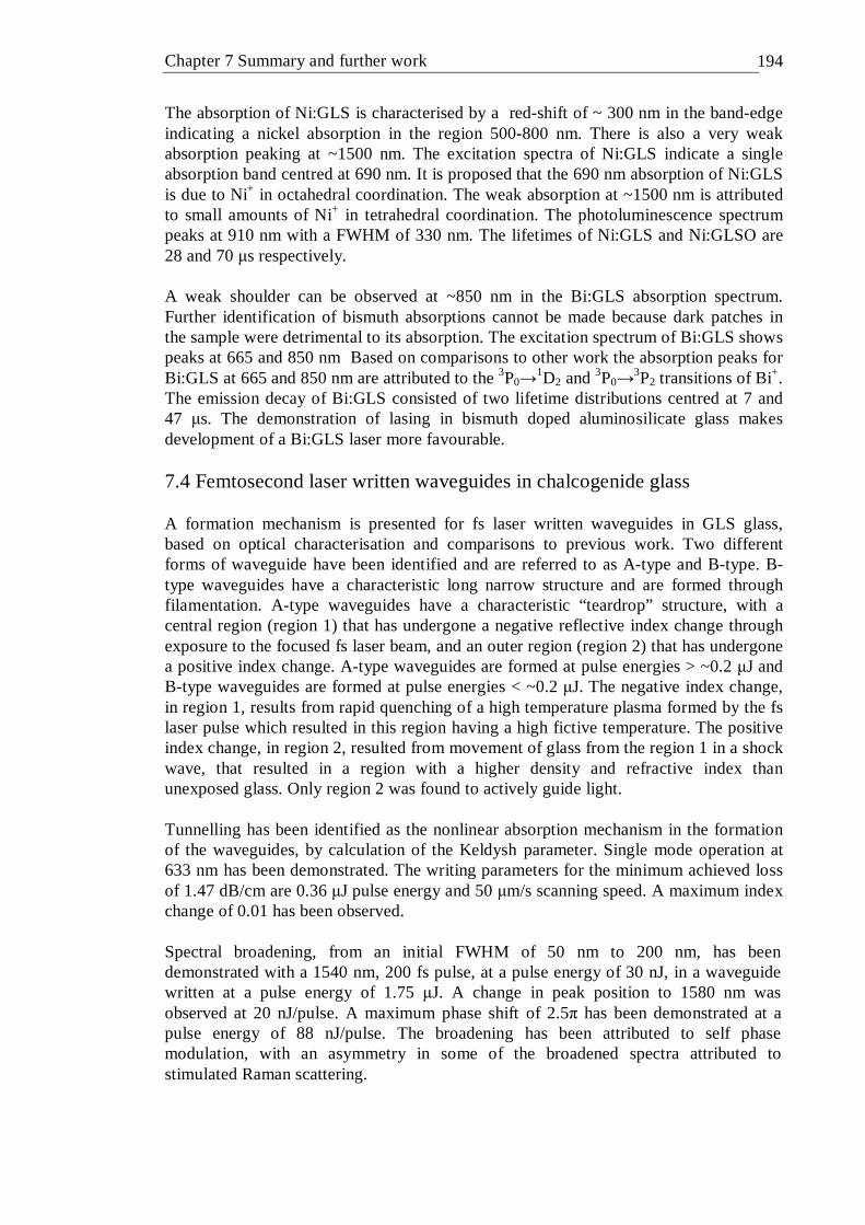
Chapter 7 Summary and further work 194
The absorption of Ni:GLS is characterised by a red-shift of ~ 300 nm in the band-edge indicating a nickel absorption in the region 500-800 nm. There is also a very weak absorption peaking at ~1500 nm. The excitation spectra of Ni:GLS indicate a single absorption band centred at 690 nm. It is proposed that the 690 nm absorption of Ni:GLS is due to Ni+ in octahedral coordination. The weak absorption at ~1500 nm is attributed to small amounts of Ni+ in tetrahedral coordination. The photoluminescence spectrum peaks at 910 nm with a FWHM of 330 nm. The lifetimes of Ni:GLS and Ni:GLSO are 28 and 70 µs respectively. A weak shoulder can be observed at ~850 nm in the Bi:GLS absorption spectrum. Further identification of bismuth absorptions cannot be made because dark patches in the sample were detrimental to its absorption. The excitation spectrum of Bi:GLS shows peaks at 665 and 850 nm Based on comparisons to other work the absorption peaks for Bi:GLS at 665 and 850 nm are attributed to the 3P0→
1D2 and 3P0→3P2 transitions of Bi+.
The emission decay of Bi:GLS consisted of two lifetime distributions centred at 7 and 47 µs. The demonstration of lasing in bismuth doped aluminosilicate glass makes development of a Bi:GLS laser more favourable. 7.4 Femtosecond laser written waveguides in chalcogenide glass A formation mechanism is presented for fs laser written waveguides in GLS glass, based on optical characterisation and comparisons to previous work. Two different forms of waveguide have been identified and are referred to as A-type and B-type. B-type waveguides have a characteristic long narrow structure and are formed through filamentation. A-type waveguides have a characteristic “teardrop” structure, with a central region (region 1) that has undergone a negative reflective index change through exposure to the focused fs laser beam, and an outer region (region 2) that has undergone a positive index change. A-type waveguides are formed at pulse energies > ~0.2 µJ and B-type waveguides are formed at pulse energies < ~0.2 µJ. The negative index change, in region 1, results from rapid quenching of a high temperature plasma formed by the fs laser pulse which resulted in this region having a high fictive temperature. The positive index change, in region 2, resulted from movement of glass from the region 1 in a shock wave, that resulted in a region with a higher density and refractive index than unexposed glass. Only region 2 was found to actively guide light. Tunnelling has been identified as the nonlinear absorption mechanism in the formation of the waveguides, by calculation of the Keldysh parameter. Single mode operation at 633 nm has been demonstrated. The writing parameters for the minimum achieved loss of 1.47 dB/cm are 0.36 µJ pulse energy and 50 µm/s scanning speed. A maximum index change of 0.01 has been observed. Spectral broadening, from an initial FWHM of 50 nm to 200 nm, has been demonstrated with a 1540 nm, 200 fs pulse, at a pulse energy of 30 nJ, in a waveguide written at a pulse energy of 1.75 µJ. A change in peak position to 1580 nm was observed at 20 nJ/pulse. A maximum phase shift of 2.5π has been demonstrated at a pulse energy of 88 nJ/pulse. The broadening has been attributed to self phase modulation, with an asymmetry in some of the broadened spectra attributed to stimulated Raman scattering.

Chapter 7 Summary and further work 195
The high nonlinearity of GLS makes it a promising material for nonlinear optical devices. An interesting effect of this nonlinearity is the spectral broadening presented in this chapter. This broadening indicates that these waveguides may have applications in nonlinear optical devices, such as a Mach-Zehnder interferometer switch or a 2R regenerator. However, the high nonlinearity of GLS frustrates the fabrication of symmetric waveguides using fs pulses because the threshold for critical self focusing appears to be higher than the threshold for material modification. 7.5 Further work The immediate further work suggested for transition metal doped chalcogenide glasses centres on the fabrication and characterisation of glass with doping concentrations that could not be investigated in this work because of the loss of ORC glass melting facilities. Some important measurements such as the quantum efficiency of Ti, Ni and Bi doped GLS could not be completed, this is therefore suggested as further work. In particular bismuth doped GLS warrants further investigation because lasing has been demonstrated in other glass hosts. Having determined the optimum doping concentration by measuring the lifetime of a range of doping concentration the fabrication of optical fibres based on V, Ti, Ni, and Bi doped GLS for possible demonstration of laser action is suggested as further work. Comparison of the spectroscopic properties of theses dopants in other chalcogenide glasses such as germanium sulphide could provide more understanding on how the phonon energy and crystal field strength of the host glass affects the quantum efficiency. This is therefore suggested as further work. Several methods for overcoming the inherent asymmetry of fs laser written waveguides in GLS have been proposed. These include using a higher NA objective, augmenting the beam profile using a slit or cylindrical lenses, using two writing beams and using a parallel writing geometry. Several methods for improving the minimum loss have been suggested. These include investigation of a greater range of translation speeds and pulse energies, using a double pulse fs laser to write the waveguides, varying the wavelength of the writing beam and annealing the sample after waveguide writing. Impressive spectral broadening was restricted to highly multimode waveguides, written at high pulse energies. Coupling sufficient pulse energy into smaller waveguides in order to observe spectral broadening is suggested as further work. A method for achieving this could be to use a tapered fibre to couple into the waveguide. Fabrication of other structures such as Fresnel zone plates and ring resonators is also suggested as further work.
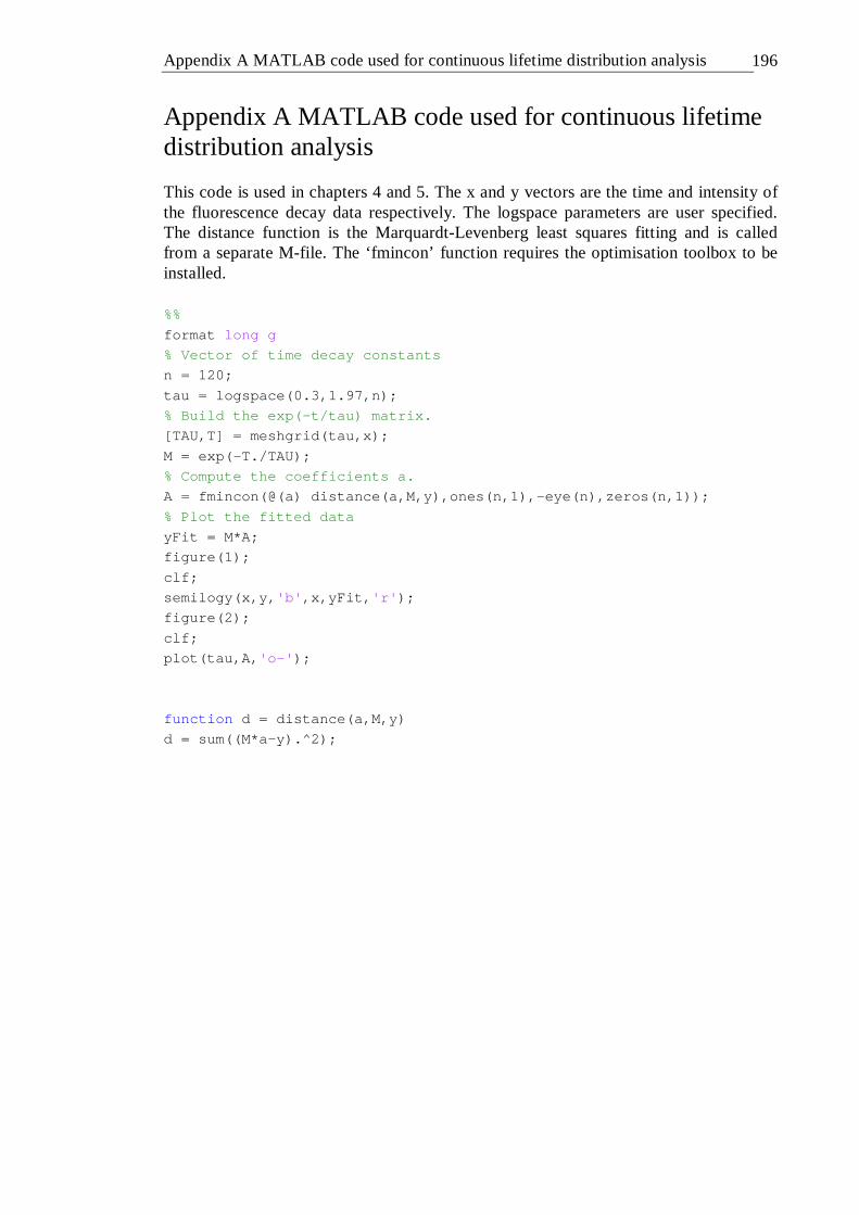
Appendix A MATLAB code used for continuous lifetime distribution analysis 196
Appendix A MATLAB code used for continuous lifetime distribution analysis
This code is used in chapters 4 and 5. The x and y vectors are the time and intensity of the fluorescence decay data respectively. The logspace parameters are user specified. The distance function is the Marquardt-Levenberg least squares fitting and is called from a separate M-file. The ‘fmincon’ function requires the optimisation toolbox to be installed.
%% format long g % Vector of time decay constants n = 120; tau = logspace(0.3,1.97,n); % Build the exp(-t/tau) matrix. [TAU,T] = meshgrid(tau,x); M = exp(-T./TAU); % Compute the coefficients a. A = fmincon(@(a) distance(a,M,y),ones(n,1),-eye(n), zeros(n,1)); % Plot the fitted data yFit = M*A; figure(1); clf; semilogy(x,y, 'b' ,x,yFit, 'r' ); figure(2); clf; plot(tau,A, 'o-' ); function d = distance(a,M,y) d = sum((M*a-y).^2);
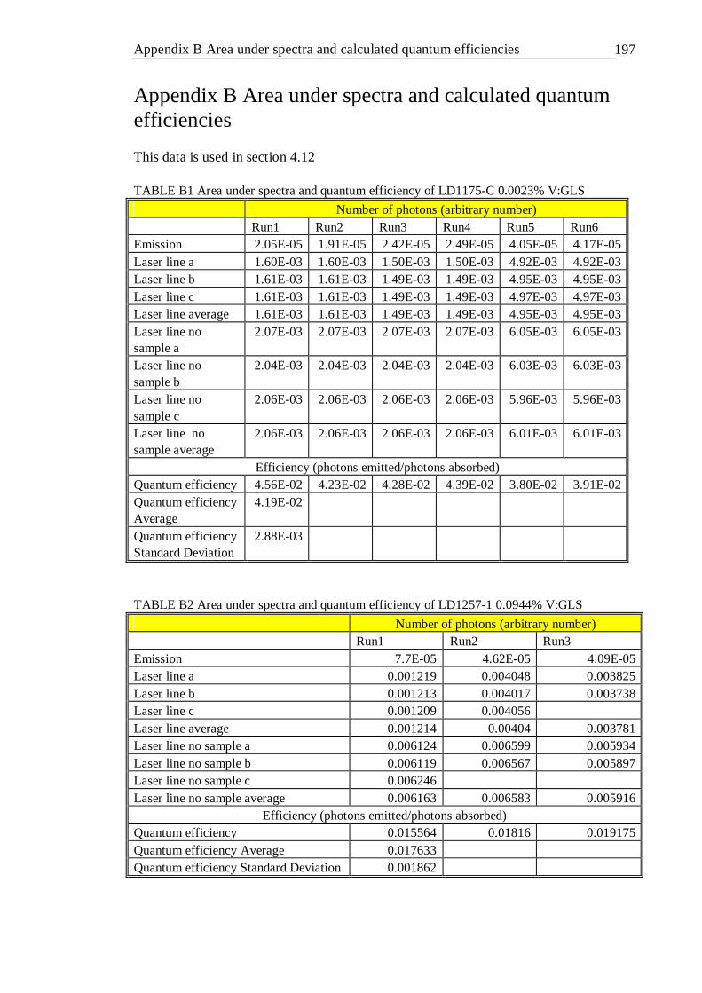
Appendix B Area under spectra and calculated quantum efficiencies 197
Appendix B Area under spectra and calculated quantum efficiencies This data is used in section 4.12 TABLE B1 Area under spectra and quantum efficiency of LD1175-C 0.0023% V:GLS
Number of photons (arbitrary number) Run1 Run2 Run3 Run4 Run5 Run6 Emission 2.05E-05 1.91E-05 2.42E-05 2.49E-05 4.05E-05 4.17E-05 Laser line a 1.60E-03 1.60E-03 1.50E-03 1.50E-03 4.92E-03 4.92E-03 Laser line b 1.61E-03 1.61E-03 1.49E-03 1.49E-03 4.95E-03 4.95E-03 Laser line c 1.61E-03 1.61E-03 1.49E-03 1.49E-03 4.97E-03 4.97E-03 Laser line average 1.61E-03 1.61E-03 1.49E-03 1.49E-03 4.95E-03 4.95E-03 Laser line no sample a
2.07E-03 2.07E-03 2.07E-03 2.07E-03 6.05E-03 6.05E-03
Laser line no sample b
2.04E-03 2.04E-03 2.04E-03 2.04E-03 6.03E-03 6.03E-03
Laser line no sample c
2.06E-03 2.06E-03 2.06E-03 2.06E-03 5.96E-03 5.96E-03
Laser line no sample average
2.06E-03 2.06E-03 2.06E-03 2.06E-03 6.01E-03 6.01E-03
Efficiency (photons emitted/photons absorbed) Quantum efficiency 4.56E-02 4.23E-02 4.28E-02 4.39E-02 3.80E-02 3.91E-02 Quantum efficiency Average
4.19E-02
Quantum efficiency Standard Deviation
2.88E-03
TABLE B2 Area under spectra and quantum efficiency of LD1257-1 0.0944% V:GLS
Number of photons (arbitrary number) Run1 Run2 Run3 Emission 7.7E-05 4.62E-05 4.09E-05 Laser line a 0.001219 0.004048 0.003825 Laser line b 0.001213 0.004017 0.003738 Laser line c 0.001209 0.004056 Laser line average 0.001214 0.00404 0.003781 Laser line no sample a 0.006124 0.006599 0.005934 Laser line no sample b 0.006119 0.006567 0.005897 Laser line no sample c 0.006246 Laser line no sample average 0.006163 0.006583 0.005916
Efficiency (photons emitted/photons absorbed) Quantum efficiency 0.015564 0.01816 0.019175 Quantum efficiency Average 0.017633 Quantum efficiency Standard Deviation 0.001862
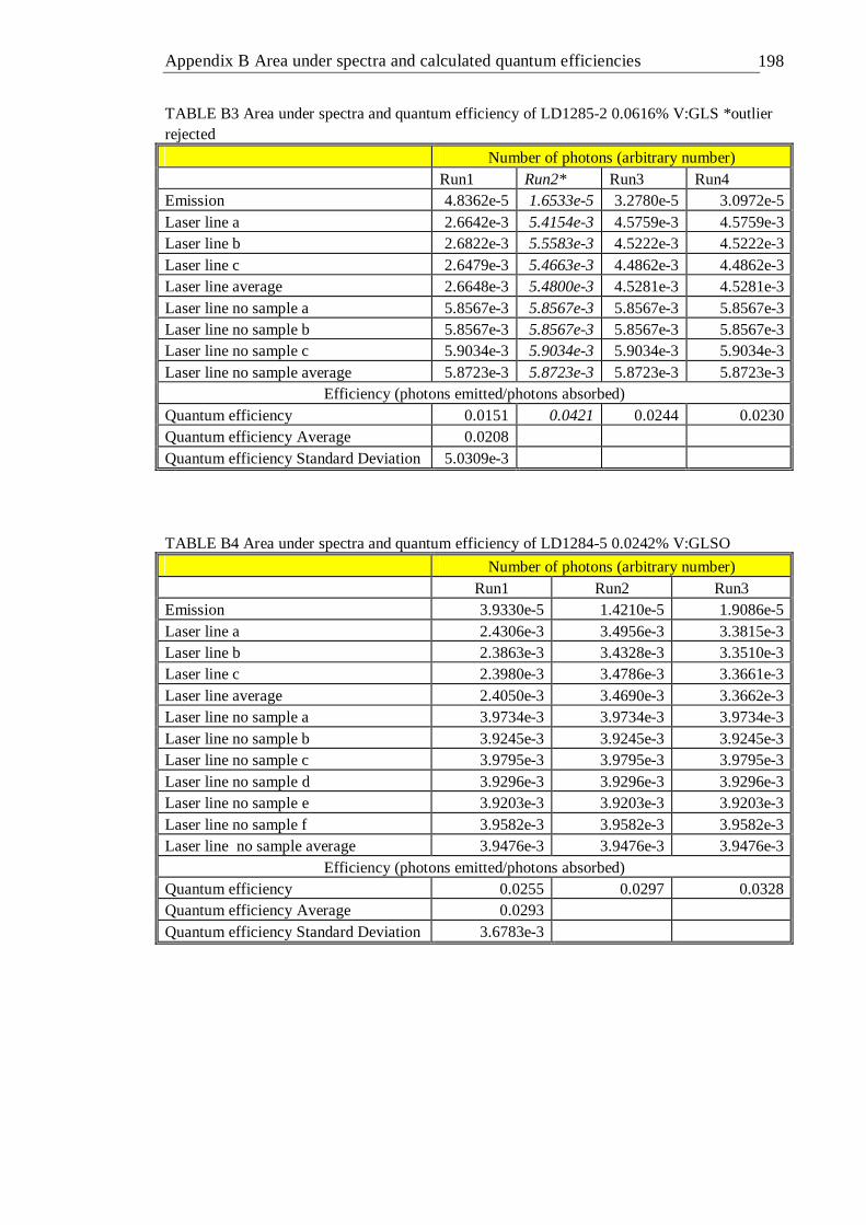
Appendix B Area under spectra and calculated quantum efficiencies 198
TABLE B3 Area under spectra and quantum efficiency of LD1285-2 0.0616% V:GLS *outlier rejected
Number of photons (arbitrary number) Run1 Run2* Run3 Run4 Emission 4.8362e-5 1.6533e-5 3.2780e-5 3.0972e-5 Laser line a 2.6642e-3 5.4154e-3 4.5759e-3 4.5759e-3 Laser line b 2.6822e-3 5.5583e-3 4.5222e-3 4.5222e-3 Laser line c 2.6479e-3 5.4663e-3 4.4862e-3 4.4862e-3 Laser line average 2.6648e-3 5.4800e-3 4.5281e-3 4.5281e-3 Laser line no sample a 5.8567e-3 5.8567e-3 5.8567e-3 5.8567e-3 Laser line no sample b 5.8567e-3 5.8567e-3 5.8567e-3 5.8567e-3 Laser line no sample c 5.9034e-3 5.9034e-3 5.9034e-3 5.9034e-3 Laser line no sample average 5.8723e-3 5.8723e-3 5.8723e-3 5.8723e-3
Efficiency (photons emitted/photons absorbed) Quantum efficiency 0.0151 0.0421 0.0244 0.0230 Quantum efficiency Average 0.0208 Quantum efficiency Standard Deviation 5.0309e-3
TABLE B4 Area under spectra and quantum efficiency of LD1284-5 0.0242% V:GLSO
Number of photons (arbitrary number) Run1 Run2 Run3 Emission 3.9330e-5 1.4210e-5 1.9086e-5 Laser line a 2.4306e-3 3.4956e-3 3.3815e-3 Laser line b 2.3863e-3 3.4328e-3 3.3510e-3 Laser line c 2.3980e-3 3.4786e-3 3.3661e-3 Laser line average 2.4050e-3 3.4690e-3 3.3662e-3 Laser line no sample a 3.9734e-3 3.9734e-3 3.9734e-3 Laser line no sample b 3.9245e-3 3.9245e-3 3.9245e-3 Laser line no sample c 3.9795e-3 3.9795e-3 3.9795e-3 Laser line no sample d 3.9296e-3 3.9296e-3 3.9296e-3 Laser line no sample e 3.9203e-3 3.9203e-3 3.9203e-3 Laser line no sample f 3.9582e-3 3.9582e-3 3.9582e-3 Laser line no sample average 3.9476e-3 3.9476e-3 3.9476e-3
Efficiency (photons emitted/photons absorbed) Quantum efficiency 0.0255 0.0297 0.0328 Quantum efficiency Average 0.0293 Quantum efficiency Standard Deviation 3.6783e-3

Appendix B Area under spectra and calculated quantum efficiencies 199
TABLE B5 Area under spectra and quantum efficiency of LD1284-4 0.0087% V:GLSO
Number of photons (arbitrary number) Run1 Run2 Run3 Run4 Emission 3.2383e-5 9.3056e-6 6.8218e-6 2.2048e-5 Laser line a 3.0896e-3 3.6146e-3 3.7073e-3 3.3512e-3 Laser line b 3.1169e-3 3.6285e-3 3.7961e-3 3.3423e-3 Laser line c 3.1258e-3 3.6050e-3 3.7081e-3 3.4037e-3 Laser line average 3.1107e-3 3.6160e-3 3.7372e-3 3.3657e-3 Laser line no sample a 3.9734e-3 3.9734e-3 3.9734e-3 3.9734e-3 Laser line no sample b 3.9245e-3 3.9245e-3 3.9245e-3 3.9245e-3 Laser line no sample c 3.9795e-3 3.9795e-3 3.9795e-3 3.9795e-3 Laser line no sample c 3.9296e-3 3.9296e-3 3.9296e-3 3.9296e-3 Laser line no sample e 3.9203e-3 3.9203e-3 3.9203e-3 3.9203e-3 Laser line no sample f 3.9582e-3 3.9582e-3 3.9582e-3 3.9582e-3 Laser line no sample average 3.9476e-3 3.9476e-3 3.9476e-3 3.9476e-3
Efficiency (photons emitted/photons absorbed) Quantum efficiency 0.0387 0.0281 0.0324 0.0379 Quantum efficiency Average 0.0343 Quantum efficiency Standard Deviation
4.9872e-3
TABLE B6 Area under spectra and quantum efficiency of LD1284-3 0.0489% V:GLSO
Number of photons (arbitrary number) Run1 Run2 Run3 Emission 3.0275e-5 9.8348e-6 2.9948e-5 Laser line a 2.2483e-3 3.4551e-3 2.2240e-3 Laser line b 2.2075e-3 3.4786e-3 2.2196e-3 Laser line c 2.1957e-3 3.5058e-3 2.2023e-3 Laser line average 2.2172e-3 3.4798e-3 2.2153e-3 Laser line no sample a 3.9734e-3 3.9734e-3 3.9734e-3 Laser line no sample b 3.9245e-3 3.9245e-3 3.9245e-3 Laser line no sample c 3.9795e-3 3.9795e-3 3.9795e-3 Laser line no sample d 3.9296e-3 3.9296e-3 3.9296e-3 Laser line no sample e 3.9203e-3 3.9203e-3 3.9203e-3 Laser line no sample f 3.9582e-3 3.9582e-3 3.9582e-3 Laser line no sample average 3.9476e-3 3.9476e-3 3.9476e-3
Efficiency (photons emitted/photons absorbed) Quantum efficiency 0.0175 0.0210 0.0173 Quantum efficiency Average 0.0186 Quantum efficiency Standard Deviation 2.0998e-3
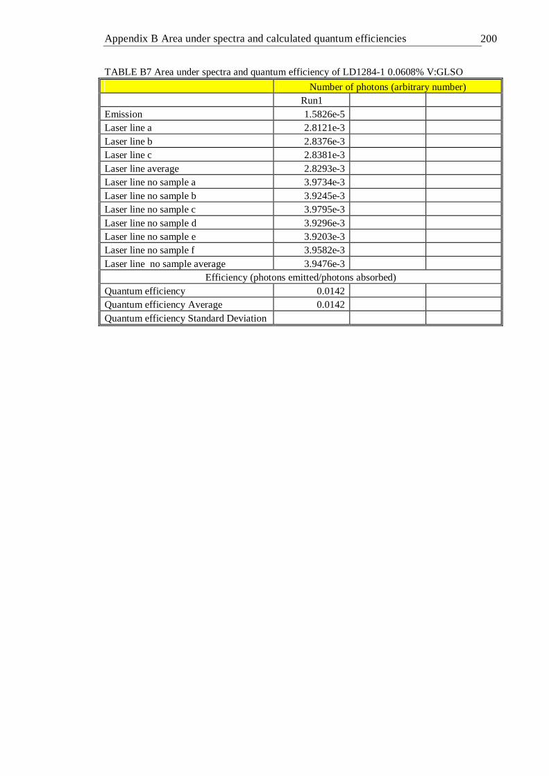
Appendix B Area under spectra and calculated quantum efficiencies 200
TABLE B7 Area under spectra and quantum efficiency of LD1284-1 0.0608% V:GLSO
Number of photons (arbitrary number) Run1 Emission 1.5826e-5 Laser line a 2.8121e-3 Laser line b 2.8376e-3 Laser line c 2.8381e-3 Laser line average 2.8293e-3 Laser line no sample a 3.9734e-3 Laser line no sample b 3.9245e-3 Laser line no sample c 3.9795e-3 Laser line no sample d 3.9296e-3 Laser line no sample e 3.9203e-3 Laser line no sample f 3.9582e-3 Laser line no sample average 3.9476e-3
Efficiency (photons emitted/photons absorbed) Quantum efficiency 0.0142 Quantum efficiency Average 0.0142 Quantum efficiency Standard Deviation

Appendix C Energy matrices and energy terms for d2 and d3 ions 201
Appendix C Energy matrices and energy terms for d2 and d3 ions These are used in section 4.16, the matrix elements are taken from reference [59]. Matrix elements for the d2 tetrahedral configuration
1A1(1G,1S)
t22 e2
10B √6(2B+C) √6(2B+C) -20Dq+8B+4C
1T2(
1D,1G) t2
2 t2e B+2C 2√3B 2√3B -10Dq+2C
1E(1D,1G)
t22 e2
B+2C -2√3B -2√3B -20Dq+2C
3T1(
3F,3P) t2
2 t2e -5B 6B 6B -10Dq+4B
t2e 1T1(1G) -10Dq+4B+2C
t2e 3T2(
3G) -10Dq-8B e2 3A2(
3F) -20Dq-8B Energy terms for the d2 tetrahedral configuration
( ) ( )22211
1 400408025100100B-20Dq918B2
1 G)(A DqCDqBDqCBCCE +++++−+=
( ) ( )22211
1 400408025100100B20Dq918B21
S)(A DqCDqBDqCBCCE ++++++−+=
( ) ( )2211 4004049B20Dq4B2
1 D)E( DqDqBCE ++−−+=
( ) ( )2211 4004049B20Dq4B2
1 G)E( DqDqBCE +++−+=
( ) ( )2212
1 1002049B10Dq4B2
1 D)(T DqDqBCE ++−−+=
( ) ( )2212
1 1002049B10Dq4B2
1 G)(T DqDqBCE +++−+=
( ) ( )2231
3 100180225B-5DqB-2
1 F)(T DqDqBE +−+=
( ) ( )2231
3 100180225B5DqB-2
1 P)(T DqDqBE +−++=
( ) CBDqE 2410 G)(T 11
1 ++−=( ) BDqE 810 G)(T 3
23 −−=
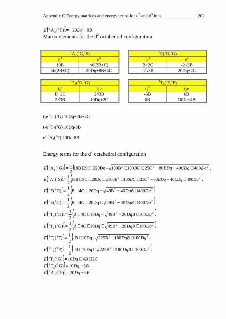
Appendix C Energy matrices and energy terms for d2 and d3 ions 202
( ) BDqE 820 F)(A 32
3 −−=
Matrix elements for the d2 octahedral configuration
1A1(1G,1S)
t22 e2
10B √6(2B+C) √6(2B+C) 20Dq+8B+4C
1T2(
1D,1G) t2
2 t2e B+2C 2√3B 2√3B 10Dq+2C
1E(1D,1G)
t22 e2
B+2C -2√3B -2√3B 20Dq+2C
3T1(
3F,3P) t2
2 t2e -5B 6B 6B 10Dq+4B
t2e 1T1(1G) 10Dq+4B+2C
t2e 3T2(
3G) 10Dq-8B e2 3A2(
3F) 20Dq-8B Energy terms for the d2 octahedral configuration
( ) ( )22211
1 400408025100100B-20Dq918B2
1 G)(A DqCDqBDqCBCCE +−−++++=
( ) ( )22211
1 400408025100100B20Dq918B2
1 S)(A DqCDqBDqCBCCE +−−+++++=
( ) ( )2211 4004049B20Dq4B2
1 D)E( DqDqBCE +−−++=
( ) ( )2211 4004049B20Dq4B2
1 G)E( DqDqBCE +−+++=
( ) ( )2212
1 1002049B10Dq4B2
1 D)(T DqDqBCE +−−++=
( ) ( )2212
1 1002049B10Dq4B2
1 G)(T DqDqBCE +−+++=
( ) ( )2231
3 100180225B-10DqB-2
1 F)(T DqDqBE +++=
( ) ( )2231
3 100180225B10DqB-2
1 P)(T DqDqBE ++++=
( ) CBDqE 2410 G)(T 11
1 ++=( ) BDqE 810 G)(T 3
23 −=
( ) BDqE 820 F)(A 32
3 −=
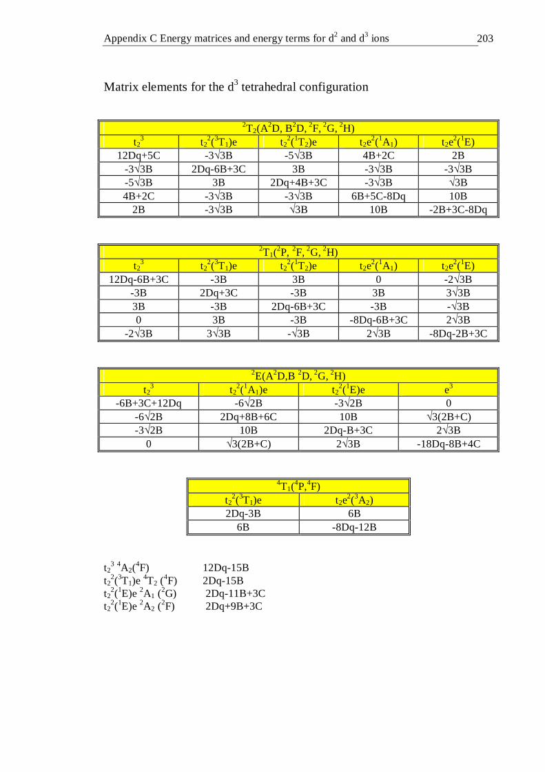
Appendix C Energy matrices and energy terms for d2 and d3 ions 203
Matrix elements for the d3 tetrahedral configuration
2T2(A2D, B2D, 2F, 2G, 2H)
t23 t2
2(3T1)e t22(1T2)e t2e
2(1A1) t2e2(1E)
12Dq+5C -3√3B -5√3B 4B+2C 2B -3√3B 2Dq-6B+3C 3B -3√3B -3√3B -5√3B 3B 2Dq+4B+3C -3√3B √3B 4B+2C -3√3B -3√3B 6B+5C-8Dq 10B
2B -3√3B √3B 10B -2B+3C-8Dq
2T1(2P, 2F, 2G, 2H)
t23 t2
2(3T1)e t22(1T2)e t2e
2(1A1) t2e2(1E)
12Dq-6B+3C -3B 3B 0 -2√3B -3B 2Dq+3C -3B 3B 3√3B 3B -3B 2Dq-6B+3C -3B -√3B 0 3B -3B -8Dq-6B+3C 2√3B
-2√3B 3√3B -√3B 2√3B -8Dq-2B+3C
2E(A2D,B 2D, 2G, 2H) t2
3 t22(1A1)e t2
2(1E)e e3 -6B+3C+12Dq -6√2B -3√2B 0
-6√2B 2Dq+8B+6C 10B √3(2B+C) -3√2B 10B 2Dq-B+3C 2√3B
0 √3(2B+C) 2√3B -18Dq-8B+4C
4T1(4P,4F)
t22(3T1)e t2e
2(3A2) 2Dq-3B 6B
6B -8Dq-12B t2
3 4A2(4F) 12Dq-15B
t22(3T1)e 4T2 (
4F) 2Dq-15B t2
2(1E)e 2A1 (2G) 2Dq-11B+3C
t22(1E)e 2A2 (
2F) 2Dq+9B+3C

Appendix C Energy matrices and energy terms for d2 and d3 ions 204
Energy terms for the d3 tetrahedral configuration
( )
=
−
−+−+++−−
+++−−−++−
= 0
184832)2(30
322311023
)2(31026826
023261236
det1)(22 I
DqCBBCB
BDqCBBB
CBBDqCBB
BBDqCB
rootGEE st λ
( )
=
−
−+−+++−−
+++−−−++−
= 0
184832)2(30
322311023
)2(31026826
023261236
det2)( 22 I
DqCBBCB
BDqCBBB
CBBDqCBB
BBDqCB
rootDaEE nd λ
( )
=
−
−+−+++−−
+++−−−++−
= 0
184832)2(30
322311023
)2(31026826
023261236
det3)(22 I
DqCBBCB
BDqCBBB
CBBDqCBB
BBDqCB
rootHEE rd λ
( )
=
−
−+−+++−−
+++−−−++−
= 0
184832)2(30
322311023
)2(31026826
023261236
det4)( 22 I
DqCBBCB
BDqCBBB
CBBDqCBB
BBDqCB
rootDbEE th λ
( )
=
−
−+−−−−+−−
−−++−−−+−
−−+−−
= 0
8323233332
32836330
3323633
3333233
320331236
det1)(21
2 I
DqCBBBBB
BDqCBBB
BBDqCBBB
BBBDqCB
BBBDqCB
rootGTE st λ
( )
=
−
−+−−−−+−−
−−++−−−+−
−−+−−
= 0
8323233332
32836330
3323633
3333233
320331236
det2)(21
2 I
DqCBBBBB
BDqCBBB
BBDqCBBB
BBBDqCB
BBBDqCB
rootHTE nd λ
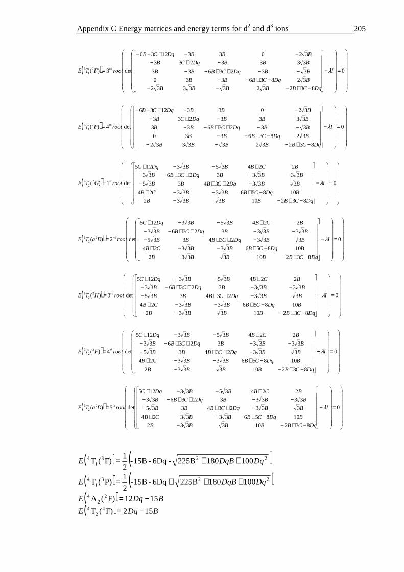
Appendix C Energy matrices and energy terms for d2 and d3 ions 205
( )
=
−
−+−−−−+−−
−−++−−−+−
−−+−−
= 0
8323233332
32836330
3323633
3333233
320331236
det3)(21
2 I
DqCBBBBB
BDqCBBB
BBDqCBBB
BBBDqCB
BBBDqCB
rootFTE rd λ
( )
=
−
−+−−−−+−−
−−++−−−+−
−−+−−
= 0
8323233332
32836330
3323633
3333233
320331236
det4)(21
2 I
DqCBBBBB
BDqCBBB
BBDqCBBB
BBBDqCB
BBBDqCB
rootPTE th λ
( )
=
−
−+−−−+−−+
−++−−−++−−
+−−+
= 0
832103332
10856333324
333234335
3333323633
2243533125
det1)(22
2 I
DqCBBBBB
BDqCBBBCB
BBDqCBBB
BBBDqCBB
BCBBBDqC
rootGTE st λ
( )
=
−
−+−−−+−−+
−++−−−++−−
+−−+
= 0
832103332
10856333324
333234335
3333323633
2243533125
det2)( 22
2 I
DqCBBBBB
BDqCBBBCB
BBDqCBBB
BBBDqCBB
BCBBBDqC
rootDaTE nd λ
( )
=
−
−+−−−+−−+
−++−−−++−−
+−−+
= 0
832103332
10856333324
333234335
3333323633
2243533125
det3)(22
2 I
DqCBBBBB
BDqCBBBCB
BBDqCBBB
BBBDqCBB
BCBBBDqC
rootHTE rd λ
( )
=
−
−+−−−+−−+
−++−−−++−−
+−−+
= 0
832103332
10856333324
333234335
3333323633
2243533125
det4)(22
2 I
DqCBBBBB
BDqCBBBCB
BBDqCBBB
BBBDqCBB
BCBBBDqC
rootFTE th λ
( )
=
−
−+−−−+−−+
−++−−−++−−
+−−+
= 0
832103332
10856333324
333234335
3333323633
2243533125
det5)( 22
2 I
DqCBBBBB
BDqCBBBCB
BBDqCBBB
BBBDqCBB
BCBBBDqC
rootDaTE th λ
( ) ( )2231
4 100180225B-6Dq-15B-2
1 F)(T DqDqBE ++=
( ) ( )2231
4 100180225B6Dq-15B-2
1 P)(T DqDqBE +++=
( ) BDqE 1512 F)(A 22
4 −=( ) BDqE 152 F)(T 4
24 −=
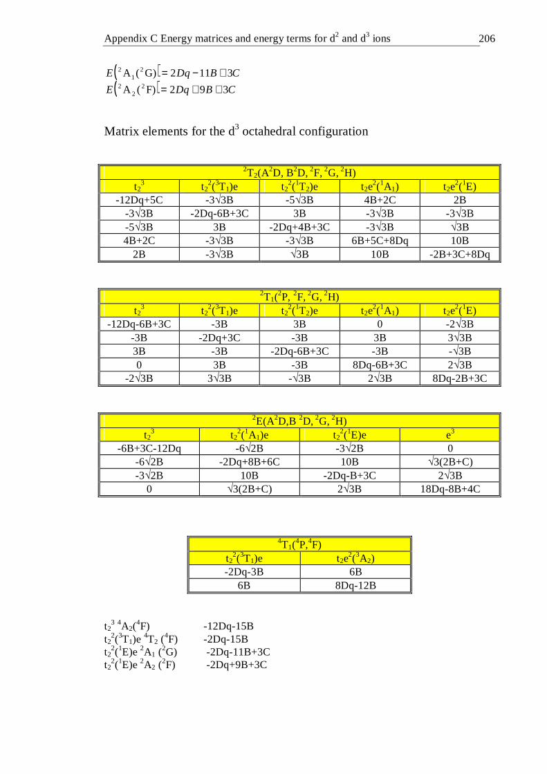
Appendix C Energy matrices and energy terms for d2 and d3 ions 206
( ) CBDqE 3112 G)(A 21
2 +−=
( ) CBDqE 392 F)(A 22
2 ++= Matrix elements for the d3 octahedral configuration
2T2(A2D, B2D, 2F, 2G, 2H)
t23 t2
2(3T1)e t22(1T2)e t2e
2(1A1) t2e2(1E)
-12Dq+5C -3√3B -5√3B 4B+2C 2B -3√3B -2Dq-6B+3C 3B -3√3B -3√3B -5√3B 3B -2Dq+4B+3C -3√3B √3B 4B+2C -3√3B -3√3B 6B+5C+8Dq 10B
2B -3√3B √3B 10B -2B+3C+8Dq
2T1(2P, 2F, 2G, 2H)
t23 t2
2(3T1)e t22(1T2)e t2e
2(1A1) t2e2(1E)
-12Dq-6B+3C -3B 3B 0 -2√3B -3B -2Dq+3C -3B 3B 3√3B 3B -3B -2Dq-6B+3C -3B -√3B 0 3B -3B 8Dq-6B+3C 2√3B
-2√3B 3√3B -√3B 2√3B 8Dq-2B+3C
2E(A2D,B 2D, 2G, 2H) t2
3 t22(1A1)e t2
2(1E)e e3 -6B+3C-12Dq -6√2B -3√2B 0
-6√2B -2Dq+8B+6C 10B √3(2B+C) -3√2B 10B -2Dq-B+3C 2√3B
0 √3(2B+C) 2√3B 18Dq-8B+4C
4T1(4P,4F)
t22(3T1)e t2e
2(3A2) -2Dq-3B 6B
6B 8Dq-12B t2
3 4A2(4F) -12Dq-15B
t22(3T1)e 4T2 (
4F) -2Dq-15B t2
2(1E)e 2A1 (2G) -2Dq-11B+3C
t22(1E)e 2A2 (
2F) -2Dq+9B+3C

Appendix C Energy matrices and energy terms for d2 and d3 ions 207
Energy terms for the d3 octahedral configuration
( )
=
−
++−+−+−−
+−+−−−−+−
= 0
184832)2(30
322311023
)2(31026826
023261236
det1)(22 I
DqCBBCB
BDqCBBB
CBBDqCBB
BBDqCB
rootGEE st λ
( )
=
−
++−+−+−−
+−+−−−−+−
= 0
184832)2(30
322311023
)2(31026826
023261236
det2)( 22 I
DqCBBCB
BDqCBBB
CBBDqCBB
BBDqCB
rootDaEE nd λ
( )
=
−
++−+−+−−
+−+−−−−+−
= 0
184832)2(30
322311023
)2(31026826
023261236
det3)(22 I
DqCBBCB
BDqCBBB
CBBDqCBB
BBDqCB
rootHEE rd λ
( )
=
−
++−+−+−−
+−+−−−−+−
= 0
184832)2(30
322311023
)2(31026826
023261236
det4)( 22 I
DqCBBCB
BDqCBBB
CBBDqCBB
BBDqCB
rootDbEE th λ
( )
=
−
++−−−++−−
−−−+−−−−−
−−−−−
= 0
8323233332
32836330
3323633
3333233
320331236
det1)(21
2 I
DqCBBBBB
BDqCBBB
BBDqCBBB
BBBDqCB
BBBDqCB
rootGTE st λ
( )
=
−
++−−−++−−
−−−+−−−−−
−−−−−
= 0
8323233332
32836330
3323633
3333233
320331236
det2)(21
2 I
DqCBBBBB
BDqCBBB
BBDqCBBB
BBBDqCB
BBBDqCB
rootHTE nd λ
( )
=
−
++−−−++−−
−−−+−−−−−
−−−−−
= 0
8323233332
32836330
3323633
3333233
320331236
det3)(21
2 I
DqCBBBBB
BDqCBBB
BBDqCBBB
BBBDqCB
BBBDqCB
rootFTE rd λ
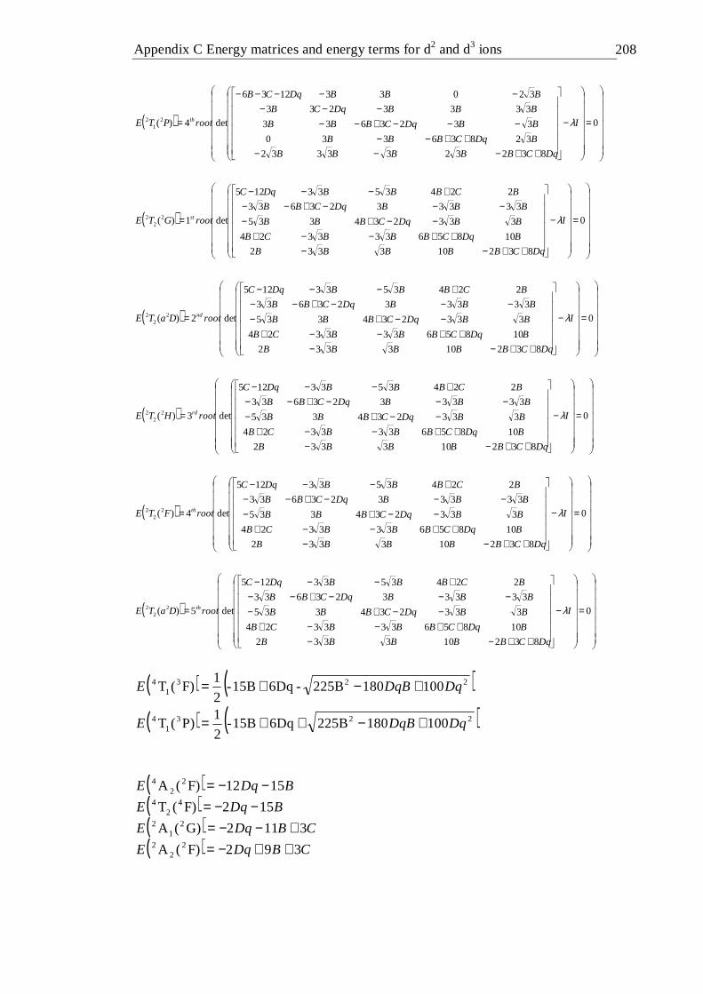
Appendix C Energy matrices and energy terms for d2 and d3 ions 208
( )
=
−
++−−−++−−
−−−+−−−−−
−−−−−
= 0
8323233332
32836330
3323633
3333233
320331236
det4)(21
2 I
DqCBBBBB
BDqCBBB
BBDqCBBB
BBBDqCB
BBBDqCB
rootPTE th λ
( )
=
−
++−−++−−+
−−+−−−−+−−
+−−−
= 0
832103332
10856333324
333234335
3333323633
2243533125
det1)(22
2 I
DqCBBBBB
BDqCBBBCB
BBDqCBBB
BBBDqCBB
BCBBBDqC
rootGTE st λ
( )
=
−
++−−++−−+
−−+−−−−+−−
+−−−
= 0
832103332
10856333324
333234335
3333323633
2243533125
det2)( 22
2 I
DqCBBBBB
BDqCBBBCB
BBDqCBBB
BBBDqCBB
BCBBBDqC
rootDaTE nd λ
( )
=
−
++−−++−−+
−−+−−−−+−−
+−−−
= 0
832103332
10856333324
333234335
3333323633
2243533125
det3)(22
2 I
DqCBBBBB
BDqCBBBCB
BBDqCBBB
BBBDqCBB
BCBBBDqC
rootHTE rd λ
( )
=
−
++−−++−−+
−−+−−−−+−−
+−−−
= 0
832103332
10856333324
333234335
3333323633
2243533125
det4)(22
2 I
DqCBBBBB
BDqCBBBCB
BBDqCBBB
BBBDqCBB
BCBBBDqC
rootFTE th λ
( )
=
−
++−−++−−+
−−+−−−−+−−
+−−−
= 0
832103332
10856333324
333234335
3333323633
2243533125
det5)( 22
2 I
DqCBBBBB
BDqCBBBCB
BBDqCBBB
BBBDqCBB
BCBBBDqC
rootDaTE th λ
( ) ( )2231
4 100180225B-6Dq15B-2
1 F)(T DqDqBE +−+=
( ) ( )2231
4 100180225B6Dq15B-2
1 P)(T DqDqBE +−++=
( ) BDqE 1512 F)(A 22
4 −−=( ) BDqE 152 F)(T 4
24 −−=
( ) CBDqE 3112 G)(A 21
2 +−−=
( ) CBDqE 392 F)(A 22
2 ++−=
Appendix D Publications 209
Appendix D
Publications Refereed publications
• M. Hughes, H. Rutt, D. Hewak, and R. Curry, Spectroscopy of vanadium (III) doped gallium lanthanum sulphide glass. Applied Physics Letters, 2007. 90(3): p. 031108.
• M. Hughes, W. Yang, and D. Hewak, Fabrication and characterization of femtosecond laser written waveguides in chalcogenide glass. Applied Physics Letters, 2007. 90(13): p. 131113.
Conference presentations, proceedings and other publications
• M. Hughes, D.W. Hewak, and R.J. Curry. Concentration dependence of the fluorescence decay profile in transition metal doped chalcogenide glass. in Photonics West. 2007. San Jose, USA: SPIE.
• M. Hughes, R.J. Curry, A. Mairaj, J.E. Aronson, W.S. Brocklesby, and D.W. Hewak. Transition metal doped chalcogenide glasses for broadband near-infrared sources. in SPIE Symposium on Optics and Photonics in Security and Defence. 2004. London.
• R.J. Curry, M. Hughes, J. Aronson, W.S. Brocklesby, and D. Hewak. Vanadium doped chalcogenide glasses for broadband near-infrared sources. in ACerS, Glass & Optical Materials Division Fall Meeting. 2004. Florida.
• A.K. Mairaj, R.J. Curry, M. Hughes, R. Simpson, K. Knight, and D.W. Hewak. Towards a compact optical waveguide device for active infrared applications. in SPIE Symposium on Optics and Photonics in Security and Defence. 2004. London.
References 210
References 1. M.N. Islam, Raman amplifiers for telecommunications. IEEE Journal of
Selected Topics in Quantum Electronics, 2002. 8(3): p. 548. 2. F.J. Duarte, Tunable Lasers Handbook. 1995: Academic Press. 3. S. Kück, Laser-related spectroscopy of ion-doped crystals for tunable solid-state
lasers. Applied Physics B, 2001. 72: p. 515-562. 4. P.F. Moulton, Spectroscopic and laser characteristics of Ti:Al203. Journal of the
Optical Society of America B, 1986. 3(1): p. 125. 5. P.F. Moulton and A. Mooradian, Broadly tuneable cw operation of NiMgF2 and
Co:MgF2 lasers. Applied Physics Letters, 1979. 35(11): p. 838. 6. U. Brauch and U. Durr, Vibronic laser action of V2+CsCaF3. Optics
Communications, 1985. 55(1): p. 35-40. 7. W. Knierim, A. Honold, U. Brauch, and U. Durr, Optical and lasing properties
of V2+ doped halide crystals. Journal of the Optical Society of America B, 1985. 3(1): p. 119-124.
8. L.F. Johnson and H.J. Guggenheim, Phonon-terminated coherent emission from V2+ ions in MgF2. Journal of Applied Physics, 1967. 38(12): p. 4837-4839.
9. S.T. Lai, B.H.T. Chai, M. Long, and M.D. Shinn, Room-temperature near-infrared tunable Cr:La3Ga5SiO14 laser. IEEE Journal of Quantum Electronics, 1988. 24(9): p. 1922–1926.
10. S.T. Lai, B.H.T. Chai, M. Long, and M.D. Shinn, Room temperature near-infrared tunable Cr:La3Ga5SiO14 laser. Quantum Electronics, IEEE Journal of, 1988. 24(9): p. 1922.
11. H. Eilers, W.M. Dennis, W.M. Yen, S. Kuck, K. Peterman, G. Huber, and W. Jia, Performance of a Cr:YAG laser. Quantum Electronics, IEEE Journal of, 1993. 29(9): p. 2508.
12. V. Yanovsky, Y. Pang, F. Wise, and B.I. Minkov, Generation of 25-fs pulses from a self-mode-locked Cr:forsterite laser with optimized group-delay dispersion. 1993. 18: p. 1541.
13. D.M. Rines, P.F. Moulton, D. Welford, and G.A. Rines, High-energy operation of a Co:MgF2 laser. Optics Letters, 1994. 19: p. 628.
14. L.E. Orgel, An Introduction to Transition Metal Chemistry. 1963: John Wiley and Sons.
15. A. Yamamoto, Organotransition Metal Chemistry - Fundamental Concepts and Applications. 1986: John Wiley & Sons.
16. T. Schweizer, F. Goutaland, E. Martins, D.W. Hewak, and W.S. Brocklesby, Site-selective spectroscopy in dysprosium-doped chalcogenide glasses for 1.3-µm optical-fiber amplifiers. Journal of the Optical Society of America B, 2001. 18(10): p. 1436-1442.
17. A. Couairon, S. Tzortzakis, L. Bergé, M. Franco, B. Prade, and A. Mysyrowicz, Infrared femtosecond light filaments in air: simulations and experiments. Journal of the Optical Society of America B, 2002. 19: p. 1117-1131.
18. C.B. Schaffer, A. Brodeur, and E. Mazur, Laser-induced breakdown and damage in bulk transparent materials induced by tightly focused femtosecond laser pulses. Materials Science and Technology, 2001. 12: p. 1784-1794.
19. J.G. Sole, L.E. Bausa, and D. Jaque, An introduction to the Optical Spectroscopy of Inorganic Solids. 2005: Wiley.
20. www.webelements.com. 2007.
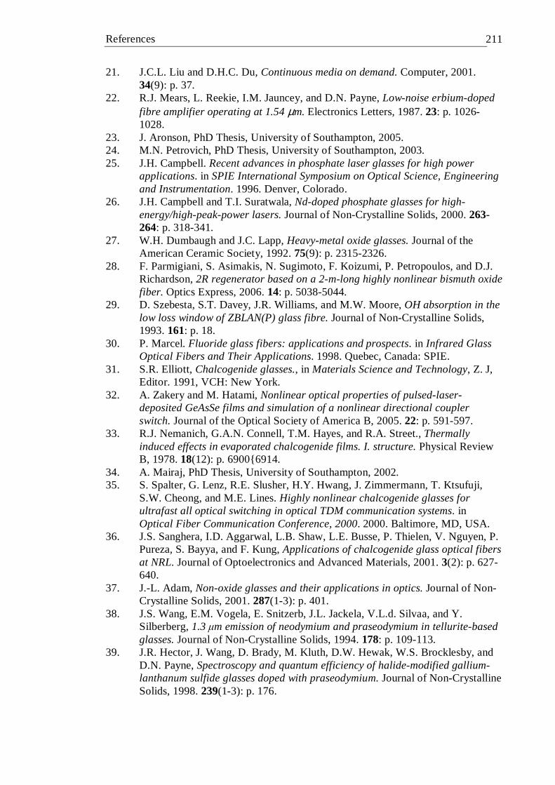
References 211
21. J.C.L. Liu and D.H.C. Du, Continuous media on demand. Computer, 2001. 34(9): p. 37.
22. R.J. Mears, L. Reekie, I.M. Jauncey, and D.N. Payne, Low-noise erbium-doped fibre amplifier operating at 1.54 µm. Electronics Letters, 1987. 23: p. 1026-1028.
23. J. Aronson, PhD Thesis, University of Southampton, 2005. 24. M.N. Petrovich, PhD Thesis, University of Southampton, 2003. 25. J.H. Campbell. Recent advances in phosphate laser glasses for high power
applications. in SPIE International Symposium on Optical Science, Engineering and Instrumentation. 1996. Denver, Colorado.
26. J.H. Campbell and T.I. Suratwala, Nd-doped phosphate glasses for high-energy/high-peak-power lasers. Journal of Non-Crystalline Solids, 2000. 263-264: p. 318-341.
27. W.H. Dumbaugh and J.C. Lapp, Heavy-metal oxide glasses. Journal of the American Ceramic Society, 1992. 75(9): p. 2315-2326.
28. F. Parmigiani, S. Asimakis, N. Sugimoto, F. Koizumi, P. Petropoulos, and D.J. Richardson, 2R regenerator based on a 2-m-long highly nonlinear bismuth oxide fiber. Optics Express, 2006. 14: p. 5038-5044.
29. D. Szebesta, S.T. Davey, J.R. Williams, and M.W. Moore, OH absorption in the low loss window of ZBLAN(P) glass fibre. Journal of Non-Crystalline Solids, 1993. 161: p. 18.
30. P. Marcel. Fluoride glass fibers: applications and prospects. in Infrared Glass Optical Fibers and Their Applications. 1998. Quebec, Canada: SPIE.
31. S.R. Elliott, Chalcogenide glasses., in Materials Science and Technology, Z. J, Editor. 1991, VCH: New York.
32. A. Zakery and M. Hatami, Nonlinear optical properties of pulsed-laser-deposited GeAsSe films and simulation of a nonlinear directional coupler switch. Journal of the Optical Society of America B, 2005. 22: p. 591-597.
33. R.J. Nemanich, G.A.N. Connell, T.M. Hayes, and R.A. Street., Thermally induced effects in evaporated chalcogenide films. I. structure. Physical Review B, 1978. 18(12): p. 69006914.
34. A. Mairaj, PhD Thesis, University of Southampton, 2002. 35. S. Spalter, G. Lenz, R.E. Slusher, H.Y. Hwang, J. Zimmermann, T. Ktsufuji,
S.W. Cheong, and M.E. Lines. Highly nonlinear chalcogenide glasses for ultrafast all optical switching in optical TDM communication systems. in Optical Fiber Communication Conference, 2000. 2000. Baltimore, MD, USA.
36. J.S. Sanghera, I.D. Aggarwal, L.B. Shaw, L.E. Busse, P. Thielen, V. Nguyen, P. Pureza, S. Bayya, and F. Kung, Applications of chalcogenide glass optical fibers at NRL. Journal of Optoelectronics and Advanced Materials, 2001. 3(2): p. 627-640.
37. J.-L. Adam, Non-oxide glasses and their applications in optics. Journal of Non-Crystalline Solids, 2001. 287(1-3): p. 401.
38. J.S. Wang, E.M. Vogela, E. Snitzerb, J.L. Jackela, V.L.d. Silvaa, and Y. Silberberg, 1.3 µm emission of neodymium and praseodymium in tellurite-based glasses. Journal of Non-Crystalline Solids, 1994. 178: p. 109-113.
39. J.R. Hector, J. Wang, D. Brady, M. Kluth, D.W. Hewak, W.S. Brocklesby, and D.N. Payne, Spectroscopy and quantum efficiency of halide-modified gallium-lanthanum sulfide glasses doped with praseodymium. Journal of Non-Crystalline Solids, 1998. 239(1-3): p. 176.
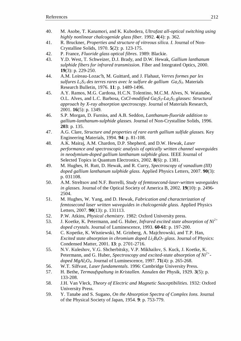
References 212
40. M. Asobe, T. Kanamori, and K. Kubodera, Ultrafast all-optical switching using highly nonlinear chalcogenide glass fiber. 1992. 4(4): p. 362.
41. R. Bruckner, Properties and structure of vitreous silica. I. Journal of Non-Crystalline Solids, 1970. 5(2): p. 123-175.
42. P. France, Fluoride glass optical fibres. 1989: Blackie. 43. Y.D. West, T. Schweizer, D.J. Brady, and D.W. Hewak, Gallium lanthanum
sulphide fibers for infrared transmission. Fiber and Integrated Optics, 2000. 19(3): p. 229-250.
44. A.M. Loireau-Lozac'h, M. Guittard, and J. Flahaut, Verres formes par les sulfures L2S3 des terres rares avec le sulfure de gallium Ga2S3. Materials Research Bulletin, 1976. 11: p. 1489-1496.
45. A.Y. Ramos, M.G. Cardona, H.C.N. Tolentino, M.C.M. Alves, N. Watanabe, O.L. Alves, and L.C. Barbosa, CsCl-modified Ga2S3-La2S3 glasses: Structural approach by X-ray absorption spectroscopy. Journal of Materials Research, 2001. 16(5): p. 1349.
46. S.P. Morgan, D. Furniss, and A.B. Seddon, Lanthanum-fluoride addition to gallium-lanthanum-sulphide glasses. Journal of Non-Crystalline Solids, 1996. 203: p. 135.
47. A.G. Clare, Structure and properties of rare earth gallium sulfide glasses. Key Engineering Materials, 1994. 94: p. 81-108.
48. A.K. Mairaj, A.M. Chardon, D.P. Shepherd, and D.W. Hewak, Laser performance and spectroscopic analysis of optically written channel waveguides in neodymium-doped gallium lanthanum sulphide glass. IEEE Journal of Selected Topics in Quantum Electronics, 2002. 8(6): p. 1381.
49. M. Hughes, H. Rutt, D. Hewak, and R. Curry, Spectroscopy of vanadium (III) doped gallium lanthanum sulphide glass. Applied Physics Letters, 2007. 90(3): p. 031108.
50. A.M. Streltsov and N.F. Borrelli, Study of femtosecond-laser-written waveguides in glasses. Journal of the Optical Society of America B, 2002. 19(10): p. 2496-2504.
51. M. Hughes, W. Yang, and D. Hewak, Fabrication and characterization of femtosecond laser written waveguides in chalcogenide glass. Applied Physics Letters, 2007. 90(13): p. 131113.
52. P.W. Atkins, Physical chemistry. 1982: Oxford University press. 53. J. Koetke, K. Petermann, and G. Huber, Infrared excited state absorption of Ni2+
doped crystals. Journal of Luminescence, 1993. 60-61: p. 197-200. 54. C. Kopetke, K. Wisniewski, M. Grinberg, A. Majchrowski, and T.P. Han,
Excited state absorption in chromium doped Li2B4O7 glass. Journal of Physics: Condensed Matter, 2001. 13: p. 2701-2716.
55. N.V. Kuleshov, V.G. Shcherbitsky, V.P. Mikhailov, S. Kuck, J. Koetke, K. Petermann, and G. Huber, Spectroscopy and excited-state absorption of Ni2+-doped MgAl2O4. Journal of Luminescence, 1997. 71(4): p. 265-268.
56. W.T. Silfvast, Laser fundamentals. 1996: Cambridge University Press. 57. H. Bethe, Termaufspaltung in Kristallen. Annalen der Physik, 1929. 3(5): p.
133-208. 58. J.H. Van Vleck, Theory of Electric and Magnetic Susceptibilities. 1932: Oxford
University Press. 59. Y. Tanabe and S. Sugano, On the Absorption Spectra of Complex Ions. Journal
of the Physical Society of Japan, 1954. 9: p. 753-779.
References 213
60. B. Henderson and G.F. Imbusch, Optical spectroscopy of inorganic solids. 1989: Oxford science publications.
61. G. Goetzt, U.W. Pohlt, and H.-J. Schulzi, Optical properties of vanadium ions in ZnSe. Journal of Physics: Condensed Matter, 1992. 4: p. 8253-8266.
62. R.S. Quimby, Active phenomena in doped halide glasses, in Fluoride Glass Fiber Optics, I.D. Aggarwal and G. Lu, Editors. 1991, Academic: New York. p. 351-396.
63. W.H. Zachariasen, The atomic arrangement in glass. Journal of the American Chemical Society, 1932. 54: p. 3841.
64. R. Fairman and B. Ushkov, Semiconducting Chalcogenide Glass I: Glass Formation, Structure, and Simulated Transformations in Chalcogenide Glasses. Vol. 78. 2004: Academic.
65. S. Benazeth, M.H. Tuilier, A.M. Loireau-Lozac'h, H. Dexpert, P. Lagarde, and J. Flahaut, An EXAFS structural approach of the lanthanum-gallium-sulfur glasses. Journal of Non-Crystalline Solids, 1989. 110(1): p. 89.
66. J. Flahaut, M. Guittard, and M. Loireau-Loozac'h, Rare earth sulphide and oxysulphide glasses. Glass Technology, 1983. 24(3): p. 149-156.
67. G. Lucazeau, S. Barnier, and M. Loireau-Loozac'h, Vibrational spectra, electronic transitions and short order structure of rare earth gallium sulphide glasses. Materials Research Bulletin, 1977. 12: p. 437-448.
68. S. Benazeth, M.H. Tuilier, H. Dexpert, M. Guittard, and D. Carre, Chalcogenide and oxychalcogenide glasses: evolution of the gallium surrounding with the oxygen content. Journal de Physique, 1986. C8(12): p. 419.
69. R. Asal, P.E. Rivers, and H.N. Rutt, A structural study of gallium lanthanum sulpdide glass bulk and thin films by X-ray absorption fine structure spectroscopy. Journal of Physics: Condensed Matter, 1997. 9: p. 6217-6230.
70. D. Brady, PhD Thesis, University of Southampton, 1999. 71. M. Avinor and G. Meijer, Vanadium activated zinc and cadmium sulphide and
selenide phosphors. Journal of the Physics and Chemistry of Solids, 1960. 12: p. 211-215.
72. S.P. Depinna and D.J. Dunstan, Frequency-resolved spectroscopy and its application to the analysis of recombination in semiconductors. Philosophical Magazine B, 1984. 50(5): p. 579-597.
73. R. Stachowitz, M. Schubert, and W. Fuhs, Frequency-resolved spectroscopy and its application to low-temperature geminate. Philosophical Magazine B, 1994. 70(6): p. 1219-1230.
74. C.E. Finlayson, A. Amezcua, P.J. Sazio, P.S. Walker, M.C. Grossel, R.J. Curry, D.C. Smith, and J.J. Baumberg, Infrared emitting PbSe nanocrystals for telecommunications window applications. Journal of Modern Optics, 2005. 52(7): p. 955-964.
75. N.C. Greenham, Measurement of absolute photoluminescence quantum efficiencies in conjugated polymers. Chemical Physics Letters, 1995. 241: p. 89-96.
76. A. Einsein, A heuristic point of view concerning the production and transformation of light. Annalen der Physik, 1905. 17: p. 132-148.
77. D. Briggs, Handbook of X-ray and ultraviolet photoelectron spectroscopy. 1977. 78. E.M.H. Goodgame DML, Smith GM, McInnes EJL, High-frequency EPR of
octahedral Mn(II) compounds with large zero-field splittings. Dalton Trans, 2003. 1: p. 34.

References 214
79. T.H. Maiman, Stimulated optical radiation in ruby. Nature, 1960. 187: p. 493–494.
80. A. Stingl, M. Lenzner, C. Spielmann, and F. Krausz, Sub-10-fs mirror-dispersion-controlled Ti:sapphire laser. Optics Letters, 1994. 20(6): p. 602-604.
81. P.C. Schultz, Optical absorption spectra of the transition elements in vitreous silica. Journal of the American Ceramic Society, 1974. 57(7): p. 309-313.
82. Y. Ohishi, S. Mitachi, T. Kanamori, and T. Manabe, Optical absorption of 3d transition metal and rare earth elements in zirconium fluoride glasses. Physics and Chemistry of Glasses, 1983. 24(5): p. 135-140.
83. Y. Suzuki, W.A. Sibley, O.H. Elbayoumi, T.M. Roberts, and B. Bendow, Optical properties of transition-metal ions in zirconium-based metal fluoride glasses andMgF2 crystals. Physical Review B, 1987. 35(9): p. 4472-4482.
84. E.M. Dianov, V.V. Dvoyrin, V.M. Mashinsky, A.A. Umnikov, M.V. Yashkov, and A.N. Gur'yanov, CW bismuth fibre laser. Quantum Electronics, 2005. 35(12): p. 1083-1084.
85. C.R. Haythornthwaite, PhD Thesis, University of Southampton, 1999. 86. W.D. Johnstone, Optical spectra of the various valence states of vanadium in
Na2O.2SiO2 glass. Journal of the American Ceramic Society, 1965. 48(12): p. 608.
87. A.G. Khudoleev and N.M. Bokin, Optical absorption and luminescence sectra of phosphate glass activated with trivalent vanadium. Journal of Applied Spectroscopy, 1971. 14(1): p. 75-76.
88. C. Mercier, G. Palavit, G. Tricot, L. Montagne, and C. Follet, A survey of transition-metal containing phosphate glasses. Comptes Rendus Chimie, 2002. 5: p. 693-703.
89. T.C. O'Haver and T. Begley, Signal-to-noise ratio in higher order derivative spectrometry. Analytical Chemistry, 1981. 53: p. 1876-1878.
90. D.W. Jordan and P. Smith, Mathematical techniques: An introduction for the engineering, physical and mathematical sciences. 1998: Oxford University press.
91. G. Talsky, Derivative Spectrophotometry. 1994: VCH. 92. W.L. Butler and D.W. Hopkins, Higher derivative analysis of complex
absorption spectra. Photochemistry and Photobiology, 1970. 14: p. 439. 93. A. Savitzky and M.J.E. Golay, Smoothing and differentiation of data by
simplified least squares procedures. Analytical Chemistry, 1964. 36(8): p. 1627-1639.
94. R.K. Brow, Oxidation states of chromium dissolved in glass determined by X-ray photoelectron spectroscopy. Journal of the American Ceramic Society, 1987. 70(6): p. 129-131.
95. M.A. Noginov, Crystal growth of vanadium doped YAlO3, LaGaO3 and CaYAlO4 crystals and spectroscopic studies of vanadium valence states. Journal of Applied Physics, 2002. 91(2): p. 569-575.
96. A.M. Malyarevich, V:YAG - a new passive Q-switch for diode pumped solid-state lasers. Applied Physics. B, 1998. 67: p. 555-558.
97. Z. Goldschmidt, W. Low, and M. Foguel, Fluorescence spectrum of trivalent vanadium in corundum. Physics Letters, 1965. 19(1): p. 17-18.
98. S. Kuck and P. Jander, Luminescence from V3+ in tetrahedral oxo-coordination. Chemical Physics Letters, 1999. 300(1-2): p. 189-194.
99. P. Peka, M.U. Lehr, and H.-J. Schulz, Vanadium centers in ZnTe crystals. I. Optical properties. Physical Review B, 1996. 53(4): p. 1907.
References 215
100. S.W. Biernacki, G. Roussos, and H.J. Schulz, The luminescence of V2+ (d3) and V3+(d2) ions in ZnS and an advanced interpretation of their excitation levels. Journal of Physics C: Solid State Physics, 1988. 21: p. 5615-5630.
101. P. Peka, H.R. Selber, H.-J. Schulz, R. Schwarz, and K.W. Benz, V+ (d4) and V2+ (d3) ion states in CdTe evidenced by photoluminescence. Solid State Communications, 1996. 98(8): p. 677-682.
102. V.V.R.K. Kumar and A.K. Bhatnagar, Effect of modifier ions on the covalency of Nd3+ ions in cadmium borate glasses. Optical Materials, 1998. 11: p. 41-51.
103. R. Moncorge and T. Benyattou, Excited-state-absorption and laser parameters of V2+ in MgF2 and KMgF3. Physical Review B, 1988. 37(16): p. 9177-9185.
104. J.N. Demas, Excited state lifetime measurements. 1983, New York: Academic press.
105. J.C. Phillips, Stretched exponential relaxation in molecular and electronic glasses. Reports on Progress in Physics, 1996. 59: p. 1133-1207.
106. R.A. Street, Luminescence in amorphous semiconductors. Advances in Physics, 1976. V25(4): p. 397.
107. A.B. Seddon, D. Furniss, M.S. Iovu, S.D. Shutov, N.N. Syrbu, A.M. Andriesh, P. Hertogen, and G.J. Adriaenssens, Optical absorption and visible luminescence in Ga-La-S-O glass doped with Pr3+ ions. Journal of Optoelectronics and Advanced Materials, 2003. 5(5): p. 1107-1113.
108. R. Chen, Apparent stretched-exponential luminescence decay in crystalline solids. Journal of Luminescence, 2003. 102-103: p. 510-518.
109. O.M. Moerner WE, Illuminating single molecules in condensed matter. Science, 1999. 283: p. 1670-1676.
110. R.A.L. Vallée, M. Cotlet, J. Hofkens, F.C.D. Schryver, and K. Mullen, Spatially heterogeneous dynamics in polymer glasses at room temperature probed by single molecule lifetime fluctuations. Macromolecules, 2003. 36(20): p. 7752 -7758.
111. K.T. G. Mauckner, T. Baier, T. Walter, and FL Sauer, Temperature-dependent lifetime distribution of the photoluminescence S-band in porous silicon. Journal of applied physics, 1993. 75(8): p. 4167-4170.
112. D.W. Marquardt, An algorithm for least squares estimation of parameters. Journal of the Society for Industrial and Applied Mathematics, 1963. 11(2): p. 431-441.
113. K. Kadono, T. Yazawa, S. Jiang, J. Porque, B.-C. Hwang, and N. Peyghambarian, Rate equation analysis and energy transfer of Er3+-doped Ga2S3–GeS2–La2S3 glasses. Journal of Non-Crystalline Solids, 2003. 331: p. 79-90.
114. S. Shen, A. Jha, S.J. Wilson, and E. Zhang, The effect of composition on the emission spectra of Tm3+-doped tellurite glasses for an S-band amplifier operating at 1.46 µm. Journal of Non-Crystalline Solids, 2003. 326: p. 510-514.
115. J. Fernandez, R. Balda, M.A. Illarramendi, and G.F. Imbusch, The relationship between quantum efficiency and average lifetime of Cr3+ ions in glass. Journal of Luminescence, 1994. 58: p. 294-297.
116. T. Aoki, S. Komedoori, S. Kobayashi, C. Fujihashi, A. Ganjoo, and K. Shimakawa, Photoluminescence lifetime distribution of a-Si:H and a-Ge:H expanded to nanosecond region using wide-band frequency-resolved spectroscopy. Journal of Non-Crystalline Solids, 2002. 299-302(1): p. 642.
117. T. Aoki, T. Shimizu, D. Saito, and K. Ikeda, Mechanism of photoluminescence in hydrogenated amorphous silicon determined by wide-band quadrature
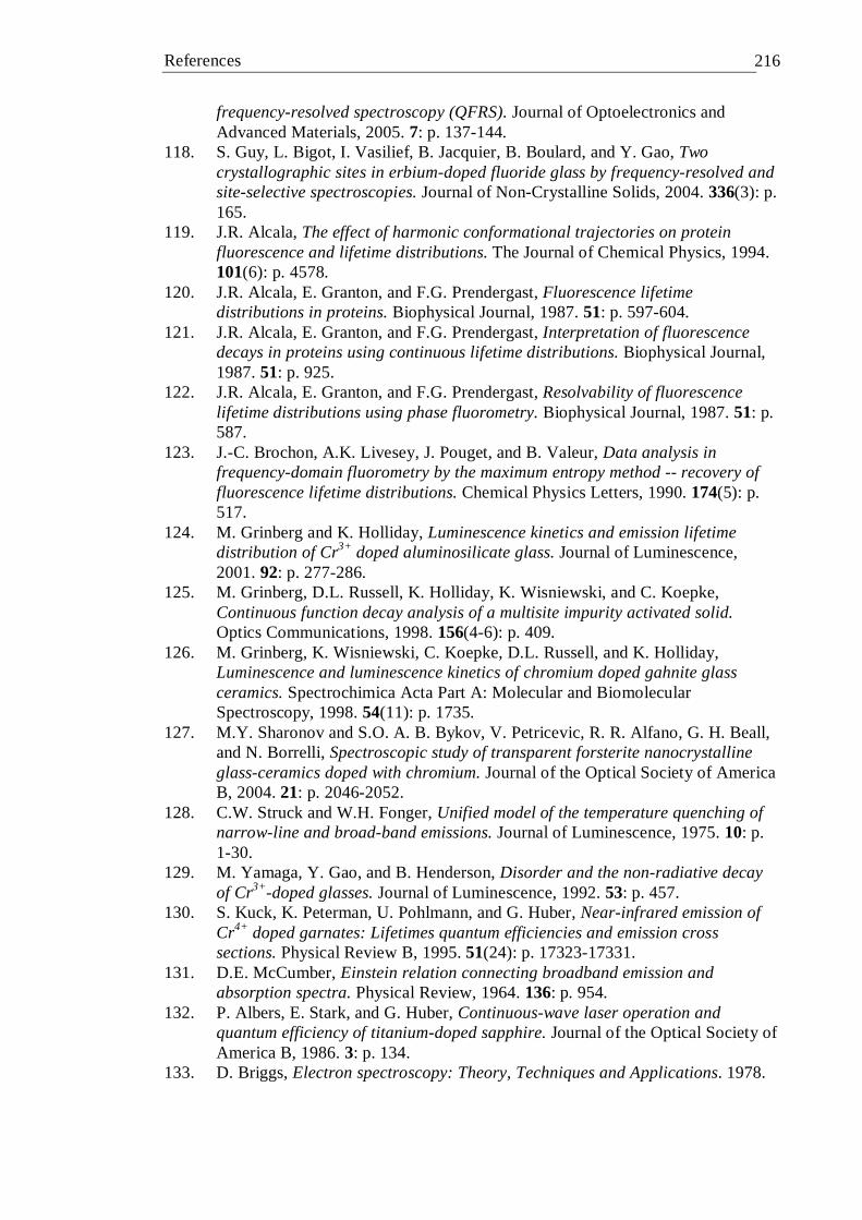
References 216
frequency-resolved spectroscopy (QFRS). Journal of Optoelectronics and Advanced Materials, 2005. 7: p. 137-144.
118. S. Guy, L. Bigot, I. Vasilief, B. Jacquier, B. Boulard, and Y. Gao, Two crystallographic sites in erbium-doped fluoride glass by frequency-resolved and site-selective spectroscopies. Journal of Non-Crystalline Solids, 2004. 336(3): p. 165.
119. J.R. Alcala, The effect of harmonic conformational trajectories on protein fluorescence and lifetime distributions. The Journal of Chemical Physics, 1994. 101(6): p. 4578.
120. J.R. Alcala, E. Granton, and F.G. Prendergast, Fluorescence lifetime distributions in proteins. Biophysical Journal, 1987. 51: p. 597-604.
121. J.R. Alcala, E. Granton, and F.G. Prendergast, Interpretation of fluorescence decays in proteins using continuous lifetime distributions. Biophysical Journal, 1987. 51: p. 925.
122. J.R. Alcala, E. Granton, and F.G. Prendergast, Resolvability of fluorescence lifetime distributions using phase fluorometry. Biophysical Journal, 1987. 51: p. 587.
123. J.-C. Brochon, A.K. Livesey, J. Pouget, and B. Valeur, Data analysis in frequency-domain fluorometry by the maximum entropy method -- recovery of fluorescence lifetime distributions. Chemical Physics Letters, 1990. 174(5): p. 517.
124. M. Grinberg and K. Holliday, Luminescence kinetics and emission lifetime distribution of Cr3+ doped aluminosilicate glass. Journal of Luminescence, 2001. 92: p. 277-286.
125. M. Grinberg, D.L. Russell, K. Holliday, K. Wisniewski, and C. Koepke, Continuous function decay analysis of a multisite impurity activated solid. Optics Communications, 1998. 156(4-6): p. 409.
126. M. Grinberg, K. Wisniewski, C. Koepke, D.L. Russell, and K. Holliday, Luminescence and luminescence kinetics of chromium doped gahnite glass ceramics. Spectrochimica Acta Part A: Molecular and Biomolecular Spectroscopy, 1998. 54(11): p. 1735.
127. M.Y. Sharonov and S.O. A. B. Bykov, V. Petricevic, R. R. Alfano, G. H. Beall, and N. Borrelli, Spectroscopic study of transparent forsterite nanocrystalline glass-ceramics doped with chromium. Journal of the Optical Society of America B, 2004. 21: p. 2046-2052.
128. C.W. Struck and W.H. Fonger, Unified model of the temperature quenching of narrow-line and broad-band emissions. Journal of Luminescence, 1975. 10: p. 1-30.
129. M. Yamaga, Y. Gao, and B. Henderson, Disorder and the non-radiative decay of Cr3+-doped glasses. Journal of Luminescence, 1992. 53: p. 457.
130. S. Kuck, K. Peterman, U. Pohlmann, and G. Huber, Near-infrared emission of Cr4+ doped garnates: Lifetimes quantum efficiencies and emission cross sections. Physical Review B, 1995. 51(24): p. 17323-17331.
131. D.E. McCumber, Einstein relation connecting broadband emission and absorption spectra. Physical Review, 1964. 136: p. 954.
132. P. Albers, E. Stark, and G. Huber, Continuous-wave laser operation and quantum efficiency of titanium-doped sapphire. Journal of the Optical Society of America B, 1986. 3: p. 134.
133. D. Briggs, Electron spectroscopy: Theory, Techniques and Applications. 1978.
References 217
134. G.A. Sawatzky and D. Post, X-Ray photoelectron and Auger spectroscopy of some vanadium oxides. Physical Review B, 1979. 20(4): p. 1546-1555.
135. R.K. Brow, Oxidation States of Chromium Dissolved in Glass Determined by X-ray Photoelectron Spectroscopy. Journal of the American Ceramic Society, 1987. 70(6): p. c129- c131.
136. D.H. A. Mekki, C.F. McConville, M. Salim, An XPS study of iron sodium silicate glass surfaces. Journal of Non-Crystalline Solids, 1996. 208: p. 267-276.
137. A. Bianconi, E. Fritsch, G. Calas, and J.Petiau, X-ray absorption near edge structure of 3d transition elements in tetrahedral coordination: The effect of bond length. Physical Review B, 1985. 32(6): p. 4292.
138. D. Prakash, V.P. Seth, I. Chand, and P. Chand, EPR study of vanadyl ion in CoO. PbO. B203 glasses. Journal of Non-Crystalline Solids, 1995.
139. S. Sen and A. Ghosh, Structural properties of strontium vanadate glasses. Journal of Materials Research, 1999. 15(4): p. 995-999.
140. L.D. Bogomolova, V.A. Jachkin, and N.A. Krasil'nikova, EPR study of vanadium-containing amorphous silica formed by sol gel method. Journal of Non-Crystalline Solids, 1998. 241: p. 13-26.
141. S. Gupta, N. Khanijo, and A. Mansingh, The influence of V4+ ion concentration on the EPR spectra of vanadate glasses. Journal of Non-Crystalline Solids, 1995. 181: p. 58-63.
142. R.B. Rao and N. Veeraiah, Study on some physical properties of Li2B2O3: V2O5 glasses. Physica B, 2004. 348: p. 256-271.
143. R.V.S.S.N. Ravikumar, V. Rajagopal Reddy, A.V. Chandrasekhar, B.J. Reddy, Y.P. Reddy, and P.S. Rao, Tetragonal site of transition metal ions doped sodium phosphate glasses. Journal of Alloys and Compounds, 2002. 337: p. 272-276.
144. R.P.S. Chakradhar, A. Murali, and J.L. Rao, A study of electron paramagnetic resonance and optical absorption spectra of VO2+ ions in alkali calcium borate glasses. Physica B, 2000. 293: p. 108-117.
145. V. Jain, EPR of VO2+ in Na2Zn(SO4)2.4H2O. Journal of Physics C, 1979. 12: p. 1403-1407.
146. J.E. Garbarczyk, L. Tykarski, P. Machowski, and M. Wasiucionek, EPR studies of mixed-conductive glasses in the AgI-Ag2O-V2O5-P2O5 system. 2001. 140(1-2): p. 141.
147. J.E. Garbarczyk, P. Machowski, M. Wasiucionek, L. Tykarski, R. Bacewicz, and A. Aleksiejuk, Studies of silver–vanadate–phosphate glasses by Raman, EPR and impedance spectroscopy methods. Solid State Ionics, 2000. 136–137: p. 1077–1083.
148. T. Murata, M. Torisaka, and H. Takebe, Compositional dependence of the valency state of Cr ions in oxide glasses. Journal of Non-Crystalline Solids, 1997. 220: p. 139-146.
149. Y.G. Choi, K.H. Kim, Y.S. Han, and J. Heo, Oxidation state and local coordination of chromium dopant in soda-lime-silicate and calcium-aluminate glasses. Chemical Physics Letters, 2000. 329: p. 370-376.
150. A. Belletti, R. Borromei, E. Cavalli, and L. Oleari, The luminescence of VO43-
ions in Ca2PO4Cl. European Journal of Solid State and Inorganic Chemistry, 1998. 35(6-7): p. 483-493.
151. T.C. Brunold, H.U. Gudel, and A.A. Kaminskii, Optical spectroscopy of V4+ doped crystals of Mg2SiO4 and Ca2GeO4. Chemical Physics Letters, 1997. 271(4-6): p. 327-334.

References 218
152. J.P. Meyn, T. Danger, K. Petermann, and G. Huber, Spectroscopic characterisation of V4+ doped Al2O3 and YAlO3. Journal of Luminescence, 1993. 55: p. 55-62.
153. M. Yamaga, B. Henderson, and Y. Yosida, Inhmogeneous broadening of electron-paramagnetic-resonance and optical spectra of V4+ in CaYAlO4. Physical Review B, 1995. 51(6): p. 3438-3448.
154. S. Sugano, Y. Tanabe, and H. Kamimura, Multiplets of transition-metal ions in crystals. 1970, New York: Academic Press.
155. V.P. Mikhailoz and N.V. Kuleshove, Optical absorption and nonlinear transmission of tetrahedral V3+(d2) in YAG. Optical Materials, 1993. 2: p. 267-272.
156. K.V. Yumashev, N.V. Kuleshov, and A.M. Malyarevich, Ultrafast dynamics of excited-state absorption in V3+:YAG crystal. Journal of Applied Physics, 1996. 80(8): p. 4782-4784.
157. M.J. Weber and L.A. Riseberg, Optical spectra of vandium ion in yttrium aluminium garnet. Journal of Chemical Physics, 1971. 55(5): p. 2032-2038.
158. M.D. Sturge, Optical spectrum of divalent vanadium in octohedral coordination. Physical Review, 1962. 120(2): p. 639-646.
159. J.S. Griffith, Theory of transition metal ions. 1961, London: Cambridge. 160. H.P. Christensen and H.P. Jenssen, Broad-band emission from chromium doped
germanium garnates. Journal of Quantum Electronics, 1982. QE-18: p. 1197. 161. C. Deka, M. Bass, B.H.T. Chai, and Y. Shimony, Optical spectroscopy of
Cr4+:Y2SiO5. Journal of the Optical Society of America B, 1993. 10: p. 1499. 162. F. Rasheed, K.P. O'Donnell, B. Henderson, and D.B. Hollis, Disorder and the
optical spectroscopy of Cr3+ doped glasses: I. Silicate glasses. Journal of Physics: Condensed Matter, 1990. 3: p. 1915-1930.
163. X. Feng, Spectroscopy and crystal-field analysis for Cr(IV) in alumino-silicate glasses. Optical Materials, 2002. 20: p. 63-72.
164. S. Kuck, K. Peterman, U. Pohlmann, and G. Huber, Electronic and vibronic transitions of the Cr4+ doped garnets LuAl5O12, Y3Al5O12, Y3Ga5O12 and Gd3Ga5O12. Journal of Luminescence, 1996. 68: p. 1-14.
165. V.V. Dvoyrin, V.M. Mashinsky, L.I. Bulatov, I.A. Bufetov, A.V. Shubin, M.A. Melkumov, E.F. Kustov, E.M. Dianov, A.A. Umnikov, V.F. Khopin, M.V. Yashkov, and A.N. Guryanov, Bismuth-doped-glass optical fibers a new active medium for lasers and amplifiers. Optics Letters, 2006. 31(20): p. 2966.
166. Y. Fujimoto and M. Nakatsuka, Infrared Luminescence from Bismuth-Doped Silica Glass. Japanese Journal of Applied Physics, 2001. 40: p. L279-L281.
167. X.-g. Meng and M.-y.P. J. -r. Qiu, D. -p. Chen, Q. -z. Zhao, X. -w. Jiang, and C. -s. Zhu, Infrared broadband emission of bismuth-doped barium-aluminum-borate glasses. Optics Express, 2005. 13(5): p. 1635.
168. X.-g. Meng and M.-y.P. J. -r. Qiu, D. -p. Chen, Q. -z. Zhao, X. -w. Jiang, and C. -s. Zhu, Near infrared broadband emission of bismuth-doped aluminophosphate glass. Optics Express, 2005. 13(5): p. 1628.
169. S. Parke and R.S. Webb, The optical properties of thallium, lead and bismuth in oxide glasses. Journal of Physics and Chemistry of Solids, 1973. 34: p. 85.
170. M. Peng, J. Qiu, D. Chen, X. Meng, I. Yang, X. Jiang, and C. Zhu, Bismuth and aluminium codoped germanium oxide glasses for super-broadband optical amplification. Optics Letters, 2004. 29(17): p. 1998.
References 219
171. M. Peng, J. Qiu, D. Chen, X. Meng, and C. Zhu, Broadband infrared luminescence from Li2O-Al2O3-ZnO-SiO2 glasses doped with Bi2O3. Optics Express, 2005. 13(18): p. 6892.
172. M. Peng, J. Qiu, D. Chen, X. Meng, and C. Zhu, Superbroadband 1310 nm emission from bismuth and tantalum codoped germanium oxide glasses. Optics Letters, 2005. 30(18): p. 2433.
173. M. Peng, C. Wang, D. Chen, J. Qiu, X. Jiang, and C. Zhu, Investigations on bismuth and aluminum co-doped germanium oxide glasses for ultra-broadband optical amplification. Journal of Non-Crystalline Solids, 2005. 351(30-32): p. 2388.
174. T. Suzuki and Y. Ohishi, Ultrabroadband near-infrared emission from Bi-doped Li2O-Al2O3-SiO2 glass. Applied Physics Letters, 2006. 88(19): p. 191912.
175. D.S. McClure, Optical Spectra of Transition-Metal Ions in Corundum. The Journal of Chemical Physics, 1962. 36(10): p. 2757-2779.
176. A. Sanchez, A.J. Strauss, R.L. Aggarwal, and R.E. Fahey, Crystal growth, spectroscopy, and laser characteristics of Ti:Al2O3. IEEE Journal of Quantum Electronics, 1988. 24(6): p. 995-1002.
177. R.L. Aggarwal, A. Sanchez, M.M. Stuppi, R.E. Fahey, A.J. Strauss, W.R. Rapoport, and C.P. Khattak, Residual infrared absorption in as-grown and annealed crystals of Ti:Al2O3. IEEE Journal of Quantum Electronics, 1988. 24(6): p. 1003.
178. S.K. Mohapatra and F.A. Kroger, Defect structure of α−Al2O3 doped with titanium. Journal of the American Ceramic Society, 1977. 60: p. 381-387.
179. K. Morinaga, H. Yoshida, and H. Takebe, Compositional dependence of absorption spectra of Ti3+ in silicate, borate, and phosphate glasses. Journal of the American Ceramic Society, 1994. 77(12): p. 3113-3118.
180. R. Balaji Rao, D. Krishna Rao, and N. Veeraiah, The role of titanium ions on structural, dielectric and optical properties of Li2O-MgO-B2O3 glass system. Materials Chemistry and Physics, 2004. 87(2-3): p. 357.
181. L.E. Bausa, J.G. Sole, A. Duran, and J.M.F. Navarro, Characterization of titanium induced optical absorption bands in phosphate glasses. Journal of Non-Crystalline Solids, 1991. 127: p. 267-272.
182. L.E. Bause, F. Jaque, J.G. Sole, and A. Duran, Photoluminescence of Ti3+ in P2O5-Na2O-Al2O3 glass. Journal of Materials Science, 1988. 23: p. 1921-1922.
183. F. Gan and H. Liu, Luminescence of titanium containing fluorophosphate glass. Journal of Luminescence, 1984. 31-32: p. 348-350.
184. N. Iwamoto, H. Hidaka, and Y. Makino, State of Ti3+ ion and Ti3+-Ti4+ redox reaction in reduced sodium silicate glasses. Journal of Non-Crystalline Solids, 1983. 58: p. 131-141.
185. G.M. Krishna, N. Veeraiah, N. Venkatramaiah, and R. Venkatesan, Induced crystallization and physical properties of Li2O-CaF2-P2O5:TiO2 glass system PART II. Electrical, magnetic and optical properties. Journal of Alloys and Compounds, 2006. In press, corrected proof.
186. A. Nolet, Optical absorption and mossbauer spectra of Fe, Ti silicate glasses. Journal of Non-Crystalline Solids, 1980. 37: p. 99-110.
187. B.S. Rawal and R.K. MacCrone, Optical absorption in an equimolar barium borosilicate glass containing titanium ions. Journal of Non-Crystalline Solids, 1978. 28: p. 337-345.
188. L.E. Bausa, F. Jaque, J.G. Sole, and A. Duran, Photoluminescence of Ti3+ in P2O5-Na2O-Al2O3 glass. Journal of Materials Science, 1988. 23: p. 1921-1922.
References 220
189. A.A. Ahmed and A.F. Abbas, Optical Absorption Characteristics of Ni2+ in Mixed-Alkali Borate Glasses. Journal of the American Ceramic Society, 1983. 66(6): p. 434-439.
190. L.D. DeLoach and R.H. Page, Transition metal doped Zinc chalcogenides: spectroscopy and laser demonstation of a new class of gain medium. Journal of Quantum Electronics, 1996. 32(6): p. 885-895.
191. C. Estournes, T. Lutz, and J.L. Guille, Reduction of nickel in soda--lime--silicate glass by hydrogen. Journal of Non-Crystalline Solids, 1996. 197(2-3): p. 192.
192. L.N. Feuerhelm and W.A. Sibley, Optical transitions of Ni2+ and radiation defects in MgF2 and MnF2. Journal of Physics C, 1983. 16: p. 799-807.
193. W. Hayes and J. Wilkens, An Investigation of the Ni+ Ion in Irradiated LiF and NaF. Proceedings of the Royal Society of London. Series A, Mathematical and Physical Sciences, 1963. 281(1386): p. 340-365.
194. L.F. Johnson, R.E. Dietz, and H.J. Guggenheim, Optical maser oscillation from Ni2+ in MgF2 involving simultaneous emission of phonons. Physical Review Letters, 1963. 11(7): p. 318.
195. P.S. May and H.U. Gudel, Infrared luminescence properties of Ni2+ in various chloride lattices: CsCdCl3, CsMgCl3, CdCl2 and MgCl2. Journal of Luminescence, 1990. 46: p. 277-290.
196. R. Pappalardo and R.E. Dietz, Absorption Spectra of Transition Ions in CdS Crystals. Physical Review, 1961. 123(4): p. 1188.
197. R.J. Sherlock, T.J. Glynn, G. Walkerb, G.F. Imbusch, and K.W. Godfrey, Spectroscopic investigations of Ni2+ in MgNb206 and ZnNb206. Journal of Luminescence, 1997. 72-74: p. 268-269.
198. T. Suzuki, G.S. Murugan, and Y. Ohishi, Optical properties of transparent Li2O--Ga2O3--SiO2 glass-ceramics embedding Ni-doped nanocrystals. Applied Physics Letters, 2005. 86(13): p. 131903.
199. T. Suzuki and Y. Ohishi, Broadband 1400 nm emission from Ni2+ in zinc-alumino-silicate glass. Applied Physics Letters, 2004. 84(19): p. 3804.
200. G. Walker, B. Kamaluddin, T.J. Glynn, and R. Sherlock, Luminescence of Ni2+ centres in forsterite (Mg2SiO4). Journal of Luminescence, 1994. 60-61: p. 123-126.
201. U. Kaufmann, W.H. Koschel, and J. Schneider, Optical and EPR study of the nickel two-electron trap state in GaP. Physical Review B, 1978. 19(7): p. 3343.
202. K.T. Stevens, N.Y. Garces, L. Bai, N.C. Giles, L.E. Halliburton, S.D. Setzler, P.G. Schunemann, T.M. Pollak, R.K. Route, and R.S. Feigelson, Optical absorption and electron-nuclear double resonance study of Ni+ ions in AgGaSe2
crystals. Journal of Physics: Condensed Matter, 2004. 16(15): p. 2593. 203. U. Kaufmann, Electronic structure of Ni+ in I-III-VI chalcopyrite
semiconductors. Physical Review B, 1975. 11(7): p. 2478. 204. G. Goetz and H.J. Schulz, Decay of internal luminescence transitions of 3d
impurities in II-IV compounds - recent experiments and refined interpretations. Journal of Luminescence, 1988. 40-41: p. 415-416.
205. Y. Fujimoto and M. Nakatsuka, Optical amplification in bismuth-doped silica glass. Applied Physics Letters, 2003. 82(19): p. 3325.
206. G. Blasse and A. Bril, Investigations on Bi3+ activated phosphors. Journal of Chemical Physics, 1968. 48(1): p. 217.
207. M.A. Hamstra, H.F. Folkerts, and G. Blasse, Red bismuth emission in alkaline-earth-metal sulfates. Journal of Materials Chemistry, 1994. 4: p. 1349.

References 221
208. R.B. Lauer, Photoluminescence in Bi12SiO20 and Bi12GeO20. Applied Physics Letters, 1970. 17(4): p. 178.
209. R. Retoux, F. Studer, C. Michel, B. Raveau, A. Fontaine, and E. Dartyge, Valence state for bismuth in the superconducting bismuth cuprates. Physical Review B, 1990. 41(1): p. 193.
210. A.M. Srivastava, Luminescence of divalent bismuth in M2+BPO5 (M2+=Ba2+,
Sr2+ and Ca2+). Journal of Luminescence, 1998. 78(4): p. 239. 211. A.C. van der Steen, J.J.A. van Hesteren, and A.P. Slok, Luminescence of the
Bi3+ Ion in Compounds LiLnO2 and NaLnO2 (Ln = Sc, Y, La, Gd, Lu). Journal of The Electrochemical Society, 1981. 128(6): p. 1327.
212. M.J. Weber and R.R. Monchamp, Luminescence of Bi4Ge3O12: Spectral and decay properties. Journal of Applied Physics, 1973. 44(12): p. 5495.
213. F. Kellendonk, T. van den Belt, and G. Blasse, On the luminescence of bismuth, cerium, and chromium and yttrium aluminium borate. The Journal of Chemical Physics, 1982. 76(3): p. 1194.
214. G. Blasse, The ultaviolet absorption bands of Bi3+ and Eu3+ in oxides. Journal of Solid State Chemistry, 1971. 4: p. 52.
215. X. Wang and H. Xia, Infrared superbroadband emission of Bi ion doped germanium-aluminum-sodium glass. Optics Communications, 2006. 268(1): p. 75.
216. G. Blasse, Unusual bismuth luminescence in strontium tetraborate (SrB4O7: Bi). Journal of Physics and Chemistry of Solids, 1994. 55: p. 171.
217. J.A. Duffy, Redox equilibria in glass. Journal of Non-Crystalline Solids, 1996. 196: p. 45.
218. S. Salem-Sugui, E.E. Alp, S.M. Mini, M. Ramanathan, J.C. Campuzano, G. Jennings, M. Faiz, S. Pei, B. Dabrowski, Y. Zheng, D.R. Richards, and D.G. Hinks, Determination of the local structure in Ba1-xKxBiO3 by x-ray-absorption spectroscopy. Physical Review B, 1991. 43(7): p. 5511.
219. B.C. Stuart, M.D. Feit, A.M. Rubenchik, B.W. Shore, and M.D. Perry, Laser-Induced Damage in Dielectrics with Nanosecond to Subpicosecond Pulses. Physical Review Letters, 1995. 74(12): p. 2248.
220. L. Shah, J. Tawney, M. Richardson, and K. Richardson, Self-Focusing During Femtosecond Micromachining of Silicate Glasses. IEEE Journal of Quantum Electronics, 2004. 40(1): p. 57-68.
221. F. Korte, S. Adams, A. Egbert, C. Fallnich, A. Ostendorf, S. Nolte, M. Will, J.-P. Ruske, B. Chichkov, and A. Tuennermann, Sub-diffraction limited structuring of solid targets with femtosecond laser pulses. Optics Express, 2000. 7: p. 41-49.
222. S. Nolte, B.N. Chichkov, H. Welling, Y. Shani, K. Lieberman, and H. Terkel, Nanostructuring with spatially localized femtosecond laser pulses. Optics Letters, 1999. 24: p. 914-916.
223. P.P. Pronko, S.K. Dutta, J. Squier, J.V. Rudd, D. Du, and G. Mourou, Machining of sub-micron holes using a femtosecond laser at 800 nm. Optics Communications, 1995. 114(1-2): p. 106.
224. R. Osellame, S. Taccheo, G. Cerullo, M. Marangoni, D. Polli, R. Ramponi, P. Laporta, and S. De Silvestri, Optical gain in Er-Yb doped waveguides fabricated by femtosecond laser pulses. Electronics Letters, 2002. 38(17): p. 964.
225. E.N. Glezer, M. Milosavljevic, L. Huang, R.J. Finlay, T.-H. Her, J.P. Callan, and E. Mazur, Three-dimensional optical storage inside transparent materials. Optics Letters, 1996. 21: p. 2023.

References 222
226. K. Yamasaki, S. Juodkazis, M. Watanabe, H.B. Sun, S. Matsuo, and H. Misawa, Recording by microexplosion and two-photon reading of three-dimensional optical memory in polymethylmethacrylate films. Applied Physics Letters, 2000. 76(8): p. 1000-1002.
227. J. Qiu, K. Miura, and K. Hirao, Three-dimensional optical memory using glasses as a recording medium through a multi-photon absorption process. Japanese Journal of Applied Physics Part 1, 2000. 37: p. 2263.
228. M. Watanabe, H. Sun, S. Juodkazis, T. Takahashi, S. Matsuo, Y. Suzuki, J. Nishii, and H. Misawa, Three-Dimensional Optical Data Storage in Vitreous Silica. Japanese Journal of Applied Physics Part 2, 1998. 37: p. 1527.
229. D. Ashkenasi, H. Varel, A. Rosenfeld, S. Henz, J. Herrmann, and E.E.B. Cambell, Application of self-focusing of ps laser pulses for three-dimensional microstructuring of transparent materials. Applied Physics Letters, 1998. 72(12): p. 1442-1444.
230. J. Qiu, Femtosecond laser induced microstructures in glass and application in mocro-optics. The Chemical Record, 2004. 4: p. 50-58.
231. J. Qiu, K. Kojima, K. Miura, T. Mitsuyu, and K. Hirao, Infrared femtosecond laser pulse induced permanent reduction of Eu3+ to Eu2+ in a fluorozirconate glass. Optics Letters, 1999. 24(11): p. 786.
232. B.P. Nelson, K.J. Blow, P.D. Constantine, N.J. Doran, J.K. Lucek, I.W. Marshall, and K. Smith, All-Optical Gbit/s Switching using Nonlinear Optical Loop Mirror. Electronics Letters, 1991. 27(9): p. 704-705.
233. K. Uchiyama, T. Morioka, and M. Saruwatari, Polarization-independent wavelength conversion using nonlinear optical loop mirror. Electronics Letters, 1995. 31(21): p. 1862-1863.
234. K.-i. Kitayama, Y. Kimura, K. Okamoto, and S. Seikai, Optical sampling using an all-fiber optical Kerr shutter. Applied Physics Letters, 1985. 46(7): p. 623.
235. E. Bricchi, J.D. Mills, P.G. Kazansky, B.G. Klappauf, and J.J. Baumberg, Birefringent Fresnel zone plates in silica fabricated by femtosecond laser machining. Optics Letters, 2002. 27(24): p. 2200-2202.
236. J.W. Chan, T.R. Huser, S.H. Risbud, J.S. Hayden, and D.M. Krol, Waveguide fabrication in phosphate glasses using femtosecond laser pulses. Applied Physics Letters, 2003. 82(15): p. 2371.
237. O.M. Efimov, L.B. Glebov, K.A. Richardson, E. Van Stryland, T. Cardinal, S.H. Park, M. Couzi, and J.L. Bruneel, Waveguide writing in chalcogenide glasses by a train of femtosecond laser pulses. Optical Materials, 2001. 17(3): p. 379.
238. J. Siegel, J.M. Fernandez-Navarro, A. Garcia-Navarro, V. Diez-Blanco, O. Sanz, J. Solis, F. Vega, and J. Armengol, Waveguide structures in heavy metal oxide glass written with femtosecond laser pulses above the critical self-focusing threshold. Applied Physics Letters, 2005. 86(12): p. 121109.
239. C. Quémarda, F. Smektala, V. Coudercb, A. Barthélémyb, and J. Lucasa, Chalcogenide glasses with high non linear optical properties for telecommunications. Journal of Physics and Chemistry of Solids, 2001. 62(8): p. 1435-1440.
240. J. Requejo-Isidro, A.K. Mairaj, V. Pruneri, D.W. Hewak, M.C. Netti, and J.J. Baumberg, Self refractive non-linearities in chalcogenide based glasses. Journal of Non-Crystalline Solids, 2003. 317(3): p. 241.
241. R. Schreieck, M. Kwakernaak, H. Jäckel, E. Gamper, E. Gini, W. Vogt, and H. Melchior, Ultrafast switching dynamics of Mach-Zehnder interferometer switches. IEEE Photonics Technology Letters, 2001. 13(6): p. 603.
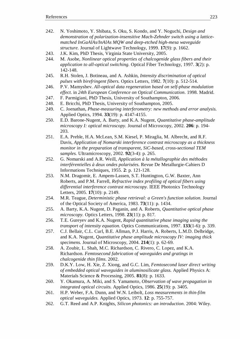
References 223
242. N. Yoshimoto, Y. Shibata, S. Oku, S. Kondo, and Y. Noguchi, Design and demonstration of polarization-insensitive Mach-Zehnder switch using a lattice-matched InGaAlAs/InAlAs MQW and deep-etched high-mesa waveguide structure. Journal of Lightwave Technology, 1999. 17(9): p. 1662.
243. J.K. Kim, PhD Thesis, Virginia State University, 2005. 244. M. Asobe, Nonlinear optical properties of chalcogenide glass fibers and their
application to all-optical switching. Optical Fiber Technology, 1997. 3(2): p. 142-148.
245. R.H. Stolen, J. Botineau, and A. Ashkin, Intensity discrimination of optical pulses with birefringent fibers. Optics Letters, 1982. 7(10): p. 512-514.
246. P.V. Mamyshev. All-optical data regeneration based on self-phase modulation effect. in 24th European Conference on Optical Communication. 1998. Madrid.
247. F. Parmigiani, PhD Thesis, University of Southampton, 2006. 248. E. Bricchi, PhD Thesis, University of Southampton, 2005. 249. C. Joenathan, Phase-measuring interferometry: new methods and error analysis.
Applied Optics, 1994. 33(19): p. 4147-4155. 250. E.D. Barone-Nugent, A. Barty, and K.A. Nugent, Quantitative phase-amplitude
microscopy I: optical microscopy. Journal of Microscopy, 2002. 206: p. 194-203.
251. E.A. Preble, H.A. McLean, S.M. Kiesel, P. Miraglia, M. Albrecht, and R.F. Davis, Application of Nomarski interference contrast microscopy as a thickness monitor in the preparation of transparent, SiC-based, cross-sectional TEM samples. Ultramicroscopy, 2002. 92(3-4): p. 265.
252. G. Nomarski and A.R. Weill, Application à la métallographie des méthodes interférentielles à deux ondes polarisées. Revue De Metallurgie-Cahiers D Informations Techniques, 1955. 2: p. 121-128.
253. N.M. Dragomir, E. Ampem-Lassen, S.T. Huntington, G.W. Baxter, Ann Roberts, and P.M. Farrell, Refractive index profiling of optical fibers using differential interference contrast microscopy. IEEE Photonics Technology Letters, 2005. 17(10): p. 2149.
254. M.R. Teague, Deterministic phase retrieval: a Green's function solution. Journal of the Optical Society of America, 1983. 73(11): p. 1434.
255. A. Barty, K.A. Nugent, D. Paganin, and A. Roberts, Quantitative optical phase microscopy. Optics Letters, 1998. 23(11): p. 817.
256. T.E. Gureyev and K.A. Nugent, Rapid quantitative phase imaging using the transport of intensity equation. Optics Communications, 1997. 133(1-6): p. 339.
257. C.J. Bellair, C.L. Curl, B.E. Allman, P.J. Harris, A. Roberts, L.M.D. Delbridge, and K.A. Nugent, Quantitative phase amplitude microscopy IV: imaging thick specimens. Journal of Microscopy, 2004. 214(1): p. 62-69.
258. A. Zoubir, L. Shah, M.C. Richardson, C. Rivero, C. Lopez, and K.A. Richardson. Femtosecond fabrication of waveguides and gratings in chalcogenide thin films. 2002.
259. D.K.Y. Low, H. Xie, Z. Xiong, and G.C. Lim, Femtosecond laser direct writing of embedded optical waveguides in aluminosilicate glass. Applied Physics A: Materials Science & Processing, 2005. 81(8): p. 1633.
260. Y. Okamura, A. Miki, and S. Yamamoto, Observation of wave propagation in integrated optical circuits. Applied Optics, 1986. 25(19): p. 3405.
261. H.P. Weber, F.A. Dunn, and W.N. Leibolt, Loss measurements in thin-film optical waveguides. Applied Optics, 1973. 12: p. 755-757.
262. G.T. Reed and A.P. Knights, Silicon photonics: an introduction. 2004: Wiley.

References 224
263. M. Will, S. Nolte, B.N. Chichkov, and A.T. nnermann, Optical properties of waveguides fabricated in fused silica by femtosecond laser pulses. Applied Optics, 2002. 41(21): p. 4360.
264. R.R. Thomson, S. Campbell, I.J. Blewett, A.K. Kar, D.T. Reid, S. Shen, and A. Jha, Active waveguide fabrication in erbium-doped oxyfluoride silicate glass using femtosecond pulses. Applied Physics Letters, 2005. 87(12): p. 121102.
265. T. Nagata, M. Kamata, and M. Obara, Optical waveguide fabrication with double pulse femtosecond lasers. Applied Physics Letters, 2005. 86(25): p. 251103.
266. R. Osellame, S. Taccheo, M. Maríangoni, R. Ramponi, P. Laporta, D. Polli, S.D. Silvestri, and G. Cerullo, Femtosecond writing of active optical waveguides with astigmatically shaped beams. Journal of the Optical Society of America B, 2003. 20(7): p. 1559-1567.
267. G.P. Agrawal, Nonlinear fiber optics. 2001, San Diego: Academic Press. 268. C.B. Schaffer, A. Brodeur, J.F. Garca, and E. Mazur, Micromachining bulk glass
by use of femtosecond laser pulses with nanojoule energy. Optics Letters, 2001. 26: p. 93-95.
269. A.L. Gaeta, Catastrophic Collapse of Ultrashort Pulses. Physical Review Letters, 2000. 84(16): p. 3582.
270. S.-H. Cho, H. Kumagai, K. Midorikawa, and M. Obara, Fabrication of double cladding structure in optical multimode fibers using plasma channeling excited by a high-intensity femtosecond laser. Optics Communications, 1999. 168(1-4): p. 287.
271. J.B. Ashcom, PhD Thesis, Harvard University, 2003. 272. J.H. Marburger, Self-focusing: Theory. Progress in Quantum Electronics, 1975.
4(1): p. 35. 273. V.R. Bhardwaj, E. Simova, P.B. Corkum, D.M. Rayner, C. Hnatovsky, R.S.
Taylor, B. Schreder, M. Kluge, and J. Zimmer, Femtosecond laser-induced refractive index modification in multicomponent glasses. Journal of Applied Physics, 2005. 97(8): p. 083102.
274. E.N. Glezer and E. Mazur, Ultrafast-laser driven micro-explosions in transparent materials. Applied Physics Letters, 1997. 71(7): p. 882-884.
275. W. Reichman, C.A. Click, and D.M. Krol. Femtosecond laser writing of waveguide structures in sodium calcium silicate glasses. in Commercial and Biomedical Applications of Ultrafast Lasers V. 2005. San Jose, CA, USA: SPIE.
276. A.Q. Tool, Relation between inelastic deformability and thermal expansion of glass in its annealing range. Journal of the American Ceramic Society, 1946. 29(9): p. 240.
277. U. Haken, O. Humbach, S. Ortner, and H. Fabian, Refractive index of silica glass: influence of fictive temperature. Journal of Non-Crystalline Solids, 2000. 265(1-2): p. 9.
278. H. Ebendorff-Heidepriem, Laser writing of waveguides in photosensitive glasses. Photonic glasses. Selected papers presented at ICO XIX, the 19th Congress of the International Commission for Optics, 2004. 25(2): p. 109.
279. A. Favre, E. Lee, V. Apostolopoulos, C.B.E. Gawith, C.-Y. Tai, E. Taylor, Y. Kondo, and F. Koizumi, Fabrication and characterization of UV-written channel waveguides in Bi2O3-based glass. Optical Materials, 2004. 27(1): p. 7.
280. K. Hirao and K. Miura, Writing waveguides and gratings in silica and related materials by a femtosecond laser. Journal of Non-Crystalline Solids, 1998. 239(1-3): p. 91.
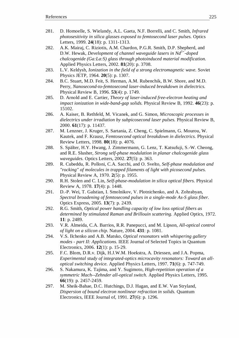
References 225
281. D. Homoelle, S. Wielandy, A.L. Gaeta, N.F. Borrelli, and C. Smith, Infrared photosesitivity in silica glasses exposed to femtosecond laser pulses. Optics Letters, 1999. 24(18): p. 1311-1313.
282. A.K. Mairaj, C. Riziotis, A.M. Chardon, P.G.R. Smith, D.P. Shepherd, and D.W. Hewak, Development of channel waveguide lasers in Nd3+-doped chalcogenide (Ga:La:S) glass through photoinduced material modification. Applied Physics Letters, 2002. 81(20): p. 3708.
283. L.V. Keldysh, Ionization in the field of a strong electromagnetic wave. Soviet Physics JETP, 1964. 20(5): p. 1307.
284. B.C. Stuart, M.D. Feit, S. Herman, A.M. Rubenchik, B.W. Shore, and M.D. Perry, Nanosecond-to-femtosecond laser-induced breakdown in dielectrics. Physical Review B, 1996. 53(4): p. 1749.
285. D. Arnold and E. Cartier, Theory of laser-induced free-electron heating and impact ionization in wide-band-gap solids. Physical Review B, 1992. 46(23): p. 15102.
286. A. Kaiser, B. Rethfeld, M. Vicanek, and G. Simon, Microscopic processes in dielectrics under irradiation by subpicosecond laser pulses. Physical Review B, 2000. 61(17): p. 11437.
287. M. Lenzner, J. Kruger, S. Sartania, Z. Cheng, C. Spielmann, G. Mourou, W. Kautek, and F. Krausz, Femtosecond optical breakdown in dielectrics. Physical Review Letters, 1998. 80(18): p. 4076.
288. S. Spälter, H.Y. Hwang, J. Zimmermann, G. Lenz, T. Katsufuji, S.-W. Cheong, and R.E. Slusher, Strong self-phase modulation in planar chalcogenide glass waveguides. Optics Letters, 2002. 27(5): p. 363.
289. R. Cubeddu, R. Polloni, C.A. Sacchi, and O. Svelto, Self-phase modulation and "rocking" of molecules in trapped filaments of light with picosecond pulses. Physical Review A, 1970. 2(5): p. 1955.
290. R.H. Stolen and C. Lin, Self-phase-modulation in silica optical fibers. Physical Review A, 1978. 17(4): p. 1448.
291. D.-P. Wei, T. Galstian, I. Smolnikov, V. Plotnichenko, and A. Zohrabyan, Spectral broadening of femtosecond pulses in a single-mode As-S glass fiber. Optics Express, 2005. 13(7): p. 2439.
292. R.G. Smith, Optical power handling capacity of low loss optical fibers as determined by stimulated Raman and Brillouin scattering. Applied Optics, 1972. 11: p. 2489.
293. V.R. Almeida, C.A. Barrios, R.R. Panepucci, and M. Lipson, All-optical control of light on a silicon chip. Nature, 2004. 431: p. 1081.
294. V.S. Ilchenko and A.B. Matsko, Optical resonators with whispering gallery modes - part II: Applications. IEEE Journal of Selected Topics in Quantum Electronics, 2006. 12(1): p. 15-29.
295. F.C. Blom, D.R.v. Dijk, H.J.W.M. Hoekstra, A. Driessen, and J.A. Popma, Experimental study of integrated-optics microcavity resonators: Toward an all-optical switching device. Applied Physics Letters, 1997. 71(6): p. 747-749.
296. S. Nakamura, K. Tajima, and Y. Sugimoto, High-repetition operation of a symmetric Mach--Zehnder all-optical switch. Applied Physics Letters, 1995. 66(19): p. 2457-2459.
297. M. Sheik-Bahae, D.C. Hutchings, D.J. Hagan, and E.W. Van Stryland, Dispersion of bound electron nonlinear refraction in solids. Quantum Electronics, IEEE Journal of, 1991. 27(6): p. 1296.

References 226
298. P. Petropoulos, T.M. Monro, W. Belardi, K. Furusawa, J.H. Lee, and D.J. Richardson, 2 R -regenerative all-optical switch based on a highly nonlinear holey fiber. Optics Letters, 2001. 26(16): p. 1233.
Related Documents


