HAL Id: tel-01127349 https://tel.archives-ouvertes.fr/tel-01127349 Submitted on 7 Mar 2015 HAL is a multi-disciplinary open access archive for the deposit and dissemination of sci- entific research documents, whether they are pub- lished or not. The documents may come from teaching and research institutions in France or abroad, or from public or private research centers. L’archive ouverte pluridisciplinaire HAL, est destinée au dépôt et à la diffusion de documents scientifiques de niveau recherche, publiés ou non, émanant des établissements d’enseignement et de recherche français ou étrangers, des laboratoires publics ou privés. Modelling the SAC microstructure evolution under thermal, thermo-mechanical and electronical constraints Lutz Meinshausen To cite this version: Lutz Meinshausen. Modelling the SAC microstructure evolution under thermal, thermo-mechanical and electronical constraints. Electronics. Université de Bordeaux, 2014. English. <NNT : 2014BORD0149>. <tel-01127349>

Welcome message from author
This document is posted to help you gain knowledge. Please leave a comment to let me know what you think about it! Share it to your friends and learn new things together.
Transcript
HAL Id: tel-01127349https://tel.archives-ouvertes.fr/tel-01127349
Submitted on 7 Mar 2015
HAL is a multi-disciplinary open accessarchive for the deposit and dissemination of sci-entific research documents, whether they are pub-lished or not. The documents may come fromteaching and research institutions in France orabroad, or from public or private research centers.
L’archive ouverte pluridisciplinaire HAL, estdestinée au dépôt et à la diffusion de documentsscientifiques de niveau recherche, publiés ou non,émanant des établissements d’enseignement et derecherche français ou étrangers, des laboratoirespublics ou privés.
Modelling the SAC microstructure evolution underthermal, thermo-mechanical and electronical constraints
Lutz Meinshausen
To cite this version:Lutz Meinshausen. Modelling the SAC microstructure evolution under thermal, thermo-mechanicaland electronical constraints. Electronics. Université de Bordeaux, 2014. English. <NNT :2014BORD0149>. <tel-01127349>

THÈSE EN COTUTELLE PRÉSENTÉE
POUR OBTENIR LE GRADE DE
DOCTEUR DE
L’UNIVERSITÉ DE BORDEAUX
ÉCOLE DOCTORALE DES SCIENCES PHYSIQUES ET DE
L’INGENIEUR
et
du GOTTFRIED WILHELM LEIBNIZ UNIVERSITÄT HANNOVER
FAKULTÄT FÜR ELEKTROTECHNIK UND INFORMATIK
SPÉCIALITÉ : Électronique
Par Lutz Meinshausen
********************************* Modeling the SAC Microstructure Evolution under Thermal,
Thermomechanical and Electrical Constraints
*********************************
Sous la direction de Hélène Frémont et de Kristen Weide-Zaage
Soutenue le 25 mars 2014 Membres du jury : Mme. Duchamp Geneviève, Professeur, Université de Bordeaux Présidente Mme. Frémont Hélène, Maitre de Conférences HdR, Université de Bordeaux Directrice Mme. Weide-Zaage Kirsten, Privatdozentin, Leibniz Universität Hannover Directrice M. Bonaud Olivier, Professeur, Université de Rennes Rapporteur M. Morris James, Professeur, Portland State University Rapporteur M. Gockenbach Ernst, Professeur, Leibniz Universität Hannover Examinateur

Titre : Modélisation de l’évolution de la microstructure d’alliage SAC sous contraintes thermiques, thermomécaniques et électriques
Résumé :
L'assemblage tridimensionnel des circuits microélectroniques et leur utilisation dans des conditions environnementales extrêmement sévères nécessitent le développement d’alternatives plus robustes pour les contacts électriques. Une technique prometteuse est la transformation des contacts de brasure conventionnelle en composés intermétalliques (IMC). Ce processus est appelé « Transient Liquid Phase Soldering » (TLPS). Dans ce contexte, des tests accélérés permettant la formation d’IMC par électromigration et thermomigration ont été effectués sur des structures « Package on Package ». L'objectif principal est le développement d'un modèle général permettant de décrire la formation des IMC dans les joints de brasure. Combiné avec une analyse par éléments finis ce modèle pourra être utilisé pour prédire la formation des IMC dans les joints de brasure pour des structures et des profils de mission différents. Le modèle de formation des IMC pourra être utilisé pour optimiser un processus TLPS.
Mots clés : Fiabilité, Brasure sans plomb, Modélisation, formation d'intermétalliques, Electromigration, Thermomigration
Title: Modeling the SAC Microstructure Evolution under Thermal, Thermo-mechanical and Electrical Constraints
Abstract: A further miniaturization of microelectronic components by three dimensional packaging, as well as the use of microelectronic devices under harsh environment conditions, requires the development of more robust alternatives to the existing Sn based solder joints. One promising technique is the diffusion and migration driven transformation of conventional solder bumps into intermetallic compound (IMC) connections. The related process is called transient liquid phase soldering (TLPS). Against this background an investigation of the IMC formation under consideration of electromigration and thermomigration was performed. For the stress tests Package on Package structures are used. The final result is a general model for the IMC formation in solder joints. Combined with a Finite Element Analysis (FEA) this model is used to predict the IMC formation in solder joints for a broad range of boundary conditions. In future the model of the IMC formation can be used to optimize a TLPS process.
Keywords: Reliability, Lead free solder, Modeling, Intermetallic Compound (IMC) formation, Transient Liquid Phase Soldering (TLPS), Electromigration, Thermomigration

- I -
Résumé
Meinshausen, Lutz
Modeling the SAC Microstructure Evolution under Thermal, Thermomechanical and Electrical
Constraints
La miniaturisation des circuits microélectroniques, leur assemblage tridimensionnel et leur utilisation
dans des conditions environnementales extrêmement sévères nécessitent le développement
d’alternatives plus robustes pour les contacts électriques. Une technique prometteuse est la
transformation des contacts de brasure conventionnelle en composé intermétallique (IMC). Ce
processus est appelé « Transient Liquid Phase Soldering « (TLPS). Le principal défi en ce qui concerne
la TLPS est la prédiction de la formation de l’IMC, en fonction de la géométrie des joints de brasure,
ou encore des conditions de fabrication. En particulier, on peut envisager d´accélérer la croissance
des IMC par électromigration (EM) et thermomigration (TM), et ces ans augmenter la température
des processus de fabrication.
Dans ce contexte, des tests accélérés permettant la formation d’IMC par TM et EM ont été effectués
sur des structures « boîtier sur boîtier » (« Package on Package » ou PoP). L'objectif principal est le
développement d'un modèle général permettant de décrire la formation des IMC dans les joints de
brasure. Combiné avec une analyse par éléments finis (FEA) ce modèle pourra être utilisé pour
prédire la formation des IMC dans les joints de brasure pour des structures et des profils de missions
différents. Pour bâtir ce modèle, plusieurs étapes ont été nécessaires.
La première étape consiste à évaluer le modèle atomique de la diffusion dans les métaux de
structure cubique à face centrée, pour les conditions spécifiques dans la structure cristalline de
composés intermétalliques Cu3Sn et Cu6Sn5.
Des tests de stockage à température élevée (TS) sont effectués sur de courtes durées et sur de
longues durées, afin de déterminer les constantes de diffusion des deux phases de croissance des
IMC. Trois autres tests à différentes températures sont effectués pour caractériser le comportement
en température de la formation des IMC.
Pour évaluer et discriminer l’influence de l’électromigration, et de la thermomigration, les
composants stockés à température élevée sont parcouru par un courant continuo un courant
alternatif de forte densité. Les résultats permettent la modélisation de la croissance des
intermétalliques sous l'influence de l’électromigration et de la thermomigration, sur la base de
paramètres indépendants de la température.
Ces paramètres matériaux sont utilisés pour paramétrer le logiciel par élément finis, afin de calculer
les flux de masse induits par la diffusion, l’électromigration et la thermomigration. La comparaison
des résultats de simulation avec les résultats expérimentaux permet de valider ces paramètres.
Finalement, les flux de masse individuels sont additionnés, et le flux total de masse est utilisé pour
calculer le développement de couche d’IMC. Une simulation dynamique est possible en divisant le
temps de test en plusieurs intervalles de temps. Ainsi, la simulation doit permettre de déterminer la
croissance de la couche intermétallique, en fonction des conditions aux limites imposées, ou de la
géométrie des joints de brasure. A l'avenir, le modèle de formation des IMC pourra être utilisé pour
optimiser un processus TLPS.

- II -
Abstract
Meinshausen, Lutz
Modeling the SAC Microstructure Evolution under Thermal, Thermomechanical and Electrical
Constraints
A further miniaturization of microelectronic components by three dimensional packaging, as well as
the use of microelectronic devices under harsh environment conditions, requires the development of
more robust alternatives to the existing Sn based solder joints. One promising technique is the
diffusion and migration driven transformation of conventional solder bumps into intermetallic
compound (IMC) connections. The related process is called transient liquid phase soldering (TLPS).
The technical challenge regarding to TLPS, and the aim of this work, is the prediction of the IMC
formation under consideration of the solder joints geometry and the chosen process parameters.
Especially the use of electromigration (EM) and thermomigration (TM) for an acceleration of the IMC
growth, without increasing the process test temperature, is of interest.
Against this background an investigation of the IMC formation under consideration of TM and EM
will be performed. For the stress tests Package on Package structures are used. The final result is a
general model for the IMC formation in solder joints. Combined with a Finite Element Analysis (FEA)
this model is used to predict the IMC formation in solder joints for a broad range of boundary
conditions. The model is approached in several intermediate steps:
As a first step of the investigation the atomic model of diffusion, being based on the conditions in fcc
metals, is evaluated for the specific conditions in the crystal lattice of the IMCs Cu3Sn and Cu6Sn5.
Long and short term temperature storage (TS) tests are performed. Knowing the long- and the short
term behavior of the diffusion driven IMC formation the tests are combined with three other TS tests
at different temperatures. The results of the short term tests are used to characterize the diffusion
driven IMC formation.
EM and TM tests at three different test temperatures are performed. For the EM and TM stress tests
TS is combined with a direct current and an alternating current. The EM and TM induced mass fluxes
values are used to characterize the migration induced IMC formation by extracting temperature
independent material parameters, being related to EM and TM.
The material values are inserted into a user developed routine for the calculation of the diffusion EM
and TM induced mass fluxes. After the validation of the material values by comparing the simulation
and the experimental results, the single migration phenomena are summarized to a total mass flux.
The total mass flux is used to calculate the IMC growth speed. A dynamic simulation of the IMC
growth becomes possible by dividing the test time into numerous time steps. The result is a FEA of
the IMC growth under consideration of the chosen boundary conditions and the three dimensional
form of the solder joints.
In future the model of the diffusion and migration driven IMC formation can be used to optimize a
TLPS process under consideration of the chosen process parameters and the form of the solder
joints.

- III -
Kurzfassung
Meinshausen, Lutz
Modeling the SAC Microstructure Evolution under Thermal, Thermomechanical and Electrical
Constraints
Die aktuellen Lötkontakte für ICs basieren auf Löthöckern aus bleifreien Zinnloten. Für die weitere
Miniaturisierung elektronischer Komponenten, oder die industrielle Anwendung von ICs unter
extremen Umweltbedingungen werden jedoch robustere Lötkontakte benötigt. Ein
vielversprechendes Verfahren ist in diesem Zusammenhang die Umwandlung einer bereits
bestehenden Lötverbindung in eine intermetallische Phase (IMC). Das dazugehörige Verfahren heißt
„Transient Liquid Phase Soldering“, kurz TLPS. Von zunehmendem Interesse für die zukünftige
Anwendung von TLPS an Bauteilen ist die Beschleunigung der Phasenumwandelung bei gleicher
Prozesstemperatur durch einen zusätzlichen Materialtransport in Folge von Elektromigration (EM)
und Thermomigration (TM).
Vor diesem Hintergrund soll die Entstehung von IMCs unter dem Einfluss von EM und TM untersucht
werden. Für die Belastungstests werden Package on Package (PoP) Strukturen verwendet. Das Ziel
der Untersuchungen ist die Entwicklung eines allgemeinen Models zur IMC Entstehung in
Lötpunkten. In Kombination mit einer Finiten Elemente Analyse (FEA) kann dieses Modell zur
Vorhersage der Wachstumsgeschwindigkeit von IMC Schichten in Lötpunkten verwendet werden.
Zu Beginn der Untersuchung wird die atomistische Theorie zur Teilchenbewegung erläutert. Dieses
Anhand einer idealisierten Kristallstruktur entworfene Modell wird dann and die besonderen
Begebenheiten in den IMCs Cu3Sn und Cu6Sn5 angepasst.
Durch eine mehrwöchige Temperaturlagerung der PoP Strukturen wird eine mögliche
Verlangsamung des IMC Wachstums bei großen Schichtdicken ermittelt. Nachdem das
Langzeitverhalten des IMC Wachstums bekannt ist, werden drei weitere Versuche bei
unterschiedlichen Temperaturen durchgeführt. Aus den daraus folgenden Daten lassen sich die
temperaturunabhängigen Materialparameter zur Beschreibung des diffusionsbedingen IMC
Wachstums extrahieren.
Für die darauf folgenden EM und TM Belastungstests wird die Temperaturlagerung mit einem
Gleichstrom und einem Wechselstrom kombiniert. Die Resultate ermöglichen eine Modellierung des
IMC Schichtwachstums unter dem Einfluss von EM und TM auf Basis von temperaturunabhängigen
Materialparametern.
Die ermittelten Materialparameter werden in selbstentwickelte Programme integriert um die
Massenflüsse durch Diffusion, EM und TM zu berechnen. Durch den Vergleich der
Simulationsergebnisse mit den Versuchsergebnissen werden die verwendeten Materialparameter
überprüft. Anschließend werden die einzelnen Massenflüsse zu einem Gesamtmassenfluss addiert,
aus dem sich auch die aktuelle Wachstumsgeschwindigkeit der IMC Schichten ergibt. Darauf
Aufbauend erlaubt eine Aufteilung der simulierten Zeitspanne in viele Einzelschritte die dynamische
Simulation des IMC Wachstums.
Die FEA erlaubt in diesem Zusammenhang die Vorhersage des IMC Schichtwachstums für eine breite
Spanne möglicher Randbedingungen, so dass die Optimierung eines TLPS Prozesses unter
Berücksichtigung der gewählten Prozessparameter und der dreidimensionalen Form der Lötpunkte
möglich wird.

- IV -
Table of Contents Abstract ................................................................................................................................................................ I
Kurzfassung ..................................................................................................................................................... III
Résumé ................................................................................................................................................................. I
Table of Contents ........................................................................................................................................... IV
List of Abbreviations and Symbols .......................................................................................................... VI
1 Introduction ............................................................................................................................................. 1
1.1 Technical and Economic Background .................................................................................................... 2
1.2 Previous Works and the Aims of this Investigation ......................................................................... 2
1.3 Content ................................................................................................................................................................ 3
2 Microelectronics Assembly and Packaging Trends ................................................................... 5
2.1 Diffusion of Innovations on the Microelectronics Market ............................................................. 6
2.2 “More Moore” and “More than Moore” ............................................................................................... 10
2.3 Three Dimensional Integration at the Package Level ................................................................... 12
2.4 Soldering Techniques for Harsh Environment Applications ..................................................... 14
2.4.1 Alternative Materials ........................................................................................................................ 15
2.4.2 Direct Bonding..................................................................................................................................... 15
2.4.3 Sintering with Nano Particles ....................................................................................................... 16
2.4.4 Comparison........................................................................................................................................... 17
2.4.5 Transient Liquid Phase Soldering ............................................................................................... 17
2.5 Influence of IMC Formation on Microelectronics Packaging Reliability ............................... 18
2.5.1 Moisture ................................................................................................................................................. 18
2.5.2 Thermal Mismatch ............................................................................................................................. 21
2.5.3 External Stress Loads ....................................................................................................................... 23
2.5.4 Electromigration ................................................................................................................................ 26
2.6 Transient Liquid Phase Soldering ......................................................................................................... 29
2.6.1 Process Design..................................................................................................................................... 29
2.6.2 Available Material Parameters ..................................................................................................... 33
2.7 Conclusion ...................................................................................................................................................... 37
3 Theory of Diffusion and the Experimental Setup ..................................................................... 38
3.1 Theory of Solid State Diffusion ............................................................................................................... 39
3.1.1 Transport Mechanisms .................................................................................................................... 39
3.1.2 The Random Walk Problem and the Diffusion Coefficient ............................................... 41
3.1.3 Derivation of the General Mass Flux Equation ....................................................................... 43
3.2 Specific Mass Flux Equations and Parameters ................................................................................ 46
3.2.1 Diffusion ................................................................................................................................................. 47
3.2.2 Electro- and Stressmigration ........................................................................................................ 47
3.2.3 Thermomigration ............................................................................................................................... 50
3.2.4 Mass Fluxes due to Differences in Solubility .......................................................................... 53

- V -
3.3 Experiments and Analysis ........................................................................................................................ 54
3.3.1 Experimental Procedure ................................................................................................................. 54
3.3.2 Experimental Setup ........................................................................................................................... 57
3.3.3 Sample Preparation and Analysis................................................................................................ 58
3.4 Migration Induced Intermetallic Compound Growth ................................................................... 60
3.4.1 General Model of Migration Induced IMC Formation ......................................................... 60
3.4.2 Adaptation of the IMC Growth Model for the Cu-Ni-Sn and Cu-Sn Formation ......... 62
3.5 Preparation of the Finite Element Analysis ...................................................................................... 65
3.5.1 Model Geometry ................................................................................................................................. 65
3.5.2 Material Parameters and the Boundary Conditions ............................................................ 68
3.5.3 Dynamic Simulation of the IMC Growth ................................................................................... 70
3.6 Conclusion ...................................................................................................................................................... 71
4 Migration Induced IMC Growth in SnAgCu Solder Bumps .................................................... 73
4.1 Long- and Short Term Behavior of IMC Formation During Temperature Storage ........... 74
4.1.1 Bottom Bumps “Open System” ..................................................................................................... 74
4.1.2 Top Bumps “Closed System” .......................................................................................................... 80
4.2 Thermomigration Induced IMC Formation....................................................................................... 84
4.2.1 General Test Results ......................................................................................................................... 84
4.2.2 Bottom Bumps “Open System” ..................................................................................................... 86
4.2.3 Top Bumps “Closed System” .......................................................................................................... 87
4.2.4 Conclusion ............................................................................................................................................. 89
4.3 Electromigration Induced IMC Formation ........................................................................................ 90
4.3.1 General Test Results ......................................................................................................................... 90
4.3.2 Bottom Bumps “Open System” ..................................................................................................... 91
4.3.3 Top Bumps “Closed System” .......................................................................................................... 96
4.4 Conclusion ................................................................................................................................................... 100
5 Simulation of the Material Transport in IMCs ......................................................................... 102
5.1 Bottom Bumps “Open System” ............................................................................................................ 103
5.1.1 Simulation of the Diffusion Induced Mass Flux .................................................................. 103
5.1.2 Simulation of the Electro- and Thermomigration Induced Mass Flux ...................... 105
5.1.3 Visualization of the IMC growth ................................................................................................ 107
5.2 Top Bumps “Closed System” ................................................................................................................ 109
5.2.1 Simulation of the Mass Flux in a Closed System During Temperature Storage .... 109
5.2.2 Simulation of the Electro- and Thermomigration Induced Mass Flux ...................... 110
5.3 Conclusion ................................................................................................................................................... 113
6 Conclusion & Perspectives ............................................................................................................. 114
6.1 Conclusion ................................................................................................................................................... 115
6.2 Perspectives ................................................................................................................................................ 117
References ..................................................................................................................................................... 118
Attachments: Curriculum Vitae and Publications ........................................................................... 133

- VI -
List of Abbreviations and Symbols
Abbreviations:
AC Alternating Current
AF Acceleration Factor
AF* Acceleration factor with downtimes
AFT Factor of Temperature Acceleration
APDL ANSYS Parameter Design Language
BGA Ball Grid Array
BSE Back Scattered Electron
C4 Controlled Collapsed Chip Connection
CAF Conductive Anodic Filaments
CME Coefficient of Moisture Expansion
CTE Coefficient of thermal expansion
CoC Chip-on-Chip
CPU Central Processing Unit
CRT Cathode Ray Tube
CSP Chip Scale Package
CTE Coefficients of Thermal Expansion
DC Direct Current
DRAM Dynamic Random-Access Memory
DIP Dual in Line Package
ECM Electrochemical Migration
EDS Energy-Dispersive X-Ray Spectroscopy
ECU Engine Control Unit
EM Electromigration
ENIG Electroless Nickel Gold
Eq. Equation
FEA Finite Element Analysis
FEM Finite Element Method
fcc face centered cubic
FR-4 Flame Retardant grade 4 (glass-reinforced epoxy laminate board)
GPU Graphics Processing Unit
GWP Growth World Product
HTC Heat Transmission Coefficient
IC Integrated Circuit
I/O Input/Output
IMC Intermetallic Compounds
MEMS Microelectromechanical Systems
MTTF Mean Time To Failure
NAND Not And gate
OSP Organic Solderability Preservative
PCB Printed Circuit Board
PoP Package on Package

- VII -
ppm parts per million
QFP Quad Flat Package
R&D Research and Development
SAB Surface-Activated Bonding
SD Standard Deviation
SE Secondary Electron
SEM Scanning Electron Microscope
SLID Solid-Liquid Interdiffusion Bonding
SMB Solid Metal Bonding
SMD Surface Mount Devices
SiP System in Package
SoC System on Chip
SSD Solid State Disk
TE Thermal Electrical
TCT Temperature Cycle Tests
TCR Temperature Coefficient of the Resistance
TCU Transmission Control Unit
TH Temperature Humidity
TM Thermomigration
TL Time Limit to saturation
TLPS Transient Liquid Phase Soldering
TS Temperature Storage
TSV Through Silicon Via
TTF Time to Failure
UTS Ultimate Tensile Strength
WLP Wafer Level Packaging
Symbols:
A Contact surface
A0 Pre exponential constant: moisture diffusion
a Lattice constant
aP Pre exponential constant: power law
α Linear temperature coefficient of Z**
αT Logarithmic growth rate: number of transistors per chip
B0 Pre exponential constant: electrochemical migration
b Logarithmic growth rate: IC package dimensions
β Driving force for material accumulation
βM Exponential term: Moisture
βTM Reduction of HM by crystal lattice/ion interactions
C Number of Input/Output contacts per package
c Exponential constant: temperature cycling tests
CM Moisture concentration
CME Coefficient of moisture expansion
D Diffusion coefficient
D0 Diffusion constant

- VIII -
DB Bump diameter
DC Contact pad diameter
d Contact diameter
δ Logarithmic growth rate: costs per fab
E Young’s Modulus
E Electric field
EA Activation energy
Ei Energy
ΔE Shift of the activation energy
e Elementary charge
ε Strain
ԑF Fermi energy
ԑ0 Vacuum permittivity
F Force
f Jumping frequency
G Thermodynamic activity
g Logarithmic growth rate: Input/Output contacts per package
gn Standard gravity
H Drop Height
Hα Energy transport by a crystal ion
HC Pre exponential constant: temperature cycling tests
HM Transport energy of the moving ion
Hm Enthalpy change per activated complex
HS Heat of solution
HV Enthalpy change per vacancy
Hγ Placement energy an ion in crystal lattice
h IMC layer thickness (chapter 2 only)
hB PCB thickness
hP Planck constant
J Mass flux density
j Current density
K Activity coefficient
KC Pre exponential constant: temperature cycling tests
kB Boltzmann constant
κ Thermal conductivity
κe Thermal conductivity by the electron gas
l Length
M Mass
M Atomic mass
m Mass fraction
mC Exponential constant: temperature cycling tests
me Electron mass
me* Effective electron mass
N Atomic density
NC Number of temperature cycles
ND Defect density

- IX -
NT Number of transistors per chip
NV Vacancy density
n Number of jumps
nA Atomic areal density
nB Exponential constant: Black equation
nP Exponential constant: power law
ni Number of atoms
η Relative volume portion of the IMC layers
Ω Atomic volume
P Pressure
p Logarithmic growth rate: growth world product
pV Probability of vacancy creation
ρ Mass density
ρel Specific resistance
Φ Electrical potential
Q Heat
Q* Heat of transport
Q*p Phonon part of Q*
Q*e Electron part of Q*
Q** Temperature dependent heat of transport value
R Total distance
r Passed distance per jump
rH Bohr radius
rh Relative humidity
S Entropy
SD Distance value
sT Thermoelectric voltage
σ Mechanical stress
σe Cross section for electron scattering
σH Hydrostatic stress
σP Cross section for phonon scattering
T Temperature
t Time
τ Lifetime of the electrons
θ Angle
U Internal energy of a closed system
u PCB deformation
μ Chemical potential
V Volume
v Velocity
vD Debye frequency
vp Speed of sound
W Work
w Jumping frequency of an atom in one direction
ω Angular acceleration
X Optional simulation result

- X -
Y Constant: Deal Grove Model
Z Valence number
ZG Constant: Deal Grove Model
Z* Effective charge of the moving ion
Z** Temperature dependent effective charge value

1 Introduction
1
1 Introduction

1 Introduction
2
1.1 Technical and Economic Background For many years the miniaturization of transistors and the resulting increase of their performance and
number per integrated circuit (IC) was the common way to create innovation. Moore's law predicted
an exponential increase of the transistors number per IC and a permanent decrease of the costs per
transistor. Unfortunately an exponential increase of costs goes along with the fulfillment of Moore's
law and as a consequence the miniaturization on transistor level reaches its economic limits.
Against this background alternatives to the miniaturization on transistor level were needed.
Alternative approaches for the exploration of new markets for microelectronic devices are the use of
ultra large scaled logic devices under harsh environment conditions or the further miniaturization of
microelectronic devices on package level by using three dimensional packaging solutions.
The melting point of conventional solders like SnAgCu is too low for the use under harsh
environment applications. The low melting point of Sn based solders also has the consequence that
they are easily affected by electromigration (EM). Reliability issues due to EM appear as a
consequence of an increasing current density due to miniaturization. Hence alternative solders have
to be used, and new connecting techniques are needed to create innovative microelectronic devices.
One promising technique for the development of future electronic devices is the diffusion driven
transformation of Sn solders into intermetallic compounds (IMC) like Cu6Sn5 or Cu3Sn. The related
process is called transient liquid phase soldering (TLPS). The main benefit of Cu-Sn IMCs compared to
common Sn based solders is the fact that their melting temperatures are a few hundred degrees
higher than the melting point of SnAgCu. Hence the temperature resistivity of IMC joints is sufficient
for harsh environment applications and they are not affected by EM induced reliability issues. IMC
joints have also proven to be very resistant against corrosion or crack formation due to
thermomechanical stress. Furthermore Cu-Sn IMCs were always present as interlayer between the
contact pads and the solder bumps. As a side effect of miniaturization they will automatically
become more and more important.
To enable the successful application of TLPS for the industrial fabrication of IMC contacts the
characterization of the IMC formation in SnAgCu solder joints under consideration of the chosen
process parameters and the form of the solder joints will be needed. Taking into account common
packaging technologies, the characterization of the diffusion induced IMC formation should cover Cu-
Sn IMCs being formed at direct Sn to Cu contacts, as well as Cu-Ni-Sn IMCs being formed in solder
joints on Ni pads.
1.2 Previous Works and the Aims of this Investigation In recent years several investigations of the diffusion driven IMC formation were performed. Based
on temperature storage (TS) tests the formation of Cu-Sn and Cu-Ni-Sn IMCs in different solders,
including SnAgCu, was investigated. Furthermore EM tests were performed. Unfortunately pure Sn
joints, instead of common solders, were used for EM tests. For the formation of Cu-Ni-Sn IMCs only a
few diffusion related parameters were available. Material values related to the TM induced IMC
formation are completely missing for all Cu-Sn and Cu-Ni-Sn IMCs. Nevertheless for the use of TLPS
the diffusion, EM and TM related material parameters are needed in a temperature independent
form.
Hence the first aim of this investigation is the determination of the required material parameters for

1 Introduction
3
the description of the diffusion and migration driven Cu-Sn and Cu-Ni-Sn formations in SnAgCu solder
joints. The second aim is the simulation of the IMC growth with the finite element method. The
required material parameters are the activation energy for atomic motion (EA), the diffusion constant
of the single components in the IMCs (D0), the effective charge of the moving ions Z* (EM parameter)
and the heat of transport Q* (TM parameter) of every single component in the different IMC layers.
Against this background several TS, EM and TM stress tests will be performed on Package on Package
(PoP) devices. The PoP devices include solder joints being directly placed on the Cu metal lines and
solder joints being placed on Ni pads. After the stress tests, the IMC formation speed and the related
mass fluxes in the IMCs will be calculated. Finally the atomic theory of diffusion enables the
parameter extraction though the mass flux values.
Afterwards ANSYS®, user developed routines and the extracted material parameters will be used for
a finite element analysis (FEA) of the IMC formation. In contrast with previous methods the FEA will
enable the investigation of the IMC formation in three dimensional structures. In future the FEA of
the IMC formation will support the development and the optimization of TLPS processes under
consideration of the chosen process parameters and the shape of the solder joints.
1.3 Content In the second chapter an overview of the economic and technical evolution of the microelectronics
market will be given. It will be shown that new packaging concepts are needed for the development
of new high-end electronics and the application of microelectronic devices under harsh environment
conditions. Based on the consequences of further progress in miniaturization, and the use profile of
harsh environment applications it will be shown that alternatives to the conventional Sn based solder
contacts are necessary to fulfill the reliability requirements for future microelectronics devices.
The transformation of Sn based solder joints into IMC joints through TLPS will be introduced as a
promising technique for the production of reliable electrical contacts for future microelectronic
devices. The benefits of TLPS will be shown by comparing it to new techniques like sintering with Ag
or Cu nano particles and by stating the promising results of previous reliability tests on IMC contacts.
In a detailed description of TLPS it will be explained why the prediction of the IMC formation speed
dependence on the solder joints dimensions and the chosen process parameters is one of the main
problems that have to be solved for an industrial application of TLPS.
Based on a principal description of the IMC formation under the influence of diffusion, EM and TM it
will be shown which material parameter must be known to predict the IMC formation speed in solder
joints. Knowing the required material parameters previous investigations will be evaluated and the
available parameters will be summarized. A comparison between the required and the available
material parameters will show which additional parameters will be needed to develop a general
model for the EM and TM driven IMC formation in SnAgCu solder joints.
At the beginning of the third chapter the atomic theory of diffusion will be explained and the related
Nernst-Einstein equation will be given. Afterwards the more specific equations of the diffusion, EM,
TM induced mass fluxes will be stated. A physical interpretation of the relevant material parameters
EA, D0, Z*, Q* will be given. Based on these interpretations it will be shown that the special conditions
in the IMCs, like the high defect density and the temperature dependent solubility of the single
components, have to be taken into account for a correct interpretation of the EM and TM induced
IMC formation. In addition the Nernst-Einstein equation will be used to develop an empirical model
of the Cu and Au accumulation due to local differences in solubility.

1 Introduction
4
Based on this theoretical background the experimental procedure for the investigation of the
diffusion and migration induced IMC growth and the following extraction of the material parameter
will be explained. It will be shown that several temperature storage (TS), TM and EM tests at
different temperatures have to be performed to get the D0 and EA, as well as temperature
independent Z* and Q* values. Furthermore the TM induced IMC formation will be investigated by a
separate stress test. For the EM stress tests TS will be combined with a direct current (DC), for the
TM stress tests an alternating current (AC) will be used. The experimental setup will be shown, and
Package on Package structures will be introduced as devices under test. The PoP structures include
direct solder to Cu contacts and solder joints on Ni pads. The direct solder to Cu contacts allow the
inflow of Cu from the metal line into the solder, while Ni pads act as diffusion barriers.
In the following, equations will be derived that enable the extraction of the mass flux values through
the average IMC formation speed during the stress tests.
Diffusion, EM and TM are exponentially temperature dependent. Hence for the interpretation of the
AC and the DC tests under consideration of Joule heating a FEA will be needed. Against this
background the PoP will be measured through light microscopy and a FE model will be designed.
Temperature measurements being performed during the DC and AC tests will be used as boundary
conditions for thermal-electrical simulations. The simulation results will show the exact test
temperature at the IMC layers under consideration of Joule heating.
In the first part of chapter four the average IMC dimensions in the top and bottom bumps before and
after the TS will be documented. Furthermore the material composition of the IMC will be
determined. In the following the mass flux values will be calculated through the average IMC
formation speed. Knowing the diffusion driven mass fluxes at different test temperatures the EA and
D0 of the single IMC components (e.g. Cu and Sn for the Cu-Sn IMCs Cu3Sn and Cu6Sn5) can be
extracted. If possible the resulting material parameters will be compared with literature values.
In the following, DC and AC tests will be performed and the mass flux values will be extracted. The
mass flux due to EM will be determined by comparing the up- and the downstream tests. The mass
flux due to TM will be extracted by subtracting the mass flux due diffusion from the average mass
flux values during the AC and the DC tests. Afterwards temperature dependent “Z**(T)” and the
“Q**(T)” values of the single IMC components can be calculated through the mass flux values. The
final temperature independent Z* values become available by taking into account the influence of
crystal defects on the electron flux. Taking into account the temperature dependent solubility of the
single components in the IMCs, also temperature independent Q* values become available.
In the last regular chapter the extracted EA, D0, Z*, Q* values will be used to calculate the mass flux
due to diffusion, EM, TM in the IMC layers. The compliance between test and simulation results will
validate the extracted material parameters. Afterwards the single mass flux values will be added to a
total mass flux. The total mass flux can be used to calculate the momentary IMC formation speed. A
dynamic simulation of the IMC growth becomes possible by dividing the test time into numerous
time steps, and by calculating the additional IMC formation for every time step. The main benefit of
the FEA is its consideration of the three dimensional geometry of the solder joints. Finally the
dynamic simulation of the IMC growth can used to predict the IMC formation during a TLPS process
under consideration of the chosen process parameters (temperature, applied current, etc.) and the
solder joint geometry.

2 Microelectronics Assembly and Packaging Trends
5
2 Microelectronics Assembly and Packaging Trends

2 Microelectronics Assembly and Packaging Trends
6
In this chapter the motivation for this work will be given by stating the main trends on the
microelectronics market and their relation to new concepts of microelectronics packaging (sections
2.1-2).
By stating the side effects of miniaturization on package level (section2.3) and the conditions for the
use of microelectronic products in the industry (section 2.4), the necessity of new techniques for the
fabrication of electrical contacts will be shown. The benefits of IMC bumps and the related TLPS
process will be shown by comparing TLPS to alternative techniques (section 2.4). Afterwards actual
investigations on the reliability of IMC bumps will be stated (section 2.5).
In the last part of the second chapter the TLPS process will be explained in detail. The technical
challenges being related to TLPS, as well as the available solutions in the literature will be shown.
Based on the detailed description of TLPS the required material parameters for a process
optimization will be stated. At least the experimental part of this work will be explained by
comparing the required material parameters with the available ones in the literature.
2.1 Diffusion of Innovations on the Microelectronics Market
The aims of research and development (R&D) in microelectronics packaging are defined by marketing
trends and consumer behavior. Following the concept “diffusion of innovations” described in [2.1]
the main difference between a successful technical breakthrough, like personal computers or smart
phones, and unsuccessful technical breakthroughs, like the unicycle, is the fact that successful
concepts were adopted by a critical number of consumers and the further process became self-
sustaining [2.1]. For new technologies their rate of diffusion in society depends on consumer
resistance to innovations [2.2]. The power of consumer resistance is due to their free will, which
simply allows the people to not buy a product even when no alternatives are available [2.3].
Furthermore, consumers are often able to create their own alternative, which was often seen in the
information technology (IT) business [2.3]. The most radical way to enforce innovation is the
elimination of the consumer’s free will. This can be done by using patents laws or by outlawing
alternatives, like it was done with light bulbs in the European Union. Of course this way to enforce
innovations has only a weak relation to R&D, because it is a more political one and it is not accessible
for many products of the microelectronics industry. Hence the focus will be on alternative ways to
enforce innovations.
Based on the time of adoption consumers are classified in five different groups [2.1]: Innovators,
early adopters, early majority, late majority and laggards. While innovators are a small group being
easy to convince and often being wealthy enough to carry high financial risks, the less flexible and
more critical early and late majority define more than two-thirds of all possible customers. The
number of users which have adopted a specific technology over time can be displayed by an S-curve
(Fig. 2.1).

2 Microelectronics Assembly and Packaging Trends
7
Figure 2.1: The five groups of possible consumers sorted by the time until adoption of an innovation (mean:
mean time to adoption; sd: standard deviation)
Based on [2.3] and [2.4] ten possible reasons of private persons, companies or organizations, to avoid
innovations can be stated:
• The usage barrier becomes relevant when private consumers or companies have to change their
daily routine or their work flow: for example long recharging times and a short driving range
slowed down the dispersion of electric cars.
• The value barrier means that, from the consumer point of view, the costs for a new product are
not in relation with its benefits compared to previous ones.
For a long time data storage devices based on integrated circuits like Solid State Disks (SSD) were
too expensive and too limited in their storage capacity to replace the available ferromagnetic
hard disks.
• The risk barrier exists because new products may include several risks, including financial risks
like a high purchase price combined with a low quality, a short lifetime of the product, or a clear
price decline when a new generation of the product appears. In addition many products, like
medical drugs, include physical risks or they could damage previous investments because of
compatibility risks.
Often PC hardware is developed with a very short time to market. Consequently problems with
compatibility and quality and a permanent price decline for new technologies appear and
prevent investments.
• Psychological barriers appear when the innovation is in conflict with regional traditions and
cultural values (e. g. skirts for men) or the responsible company/institution has image problems.

2 Microelectronics Assembly and Packaging Trends
8
In addition companies have to face several economic risks during development [2.3-4].
• Access to market barrier: the company does not have a foot print on the relevant market or an
infrastructure to sell the product. For example software has to be compatible with a limited
number of existing operating systems.
• Expertise barrier: Companies often specialize in a specific field and they try to improve their
efficiency instead of making experiments on new fields. As a consequence companies have
problems to follow rapid innovations on the market or they have problems to reach new
markets. For example during the change from cathode ray tube (CRT) monitors to flat screens
most European companies in that field were replaced by competitors. The expertise barrier is
more a management than a R&D problem. It can be overcome by joint ventures, with research
alliances including other companies and universities, or by acquisition of innovators [2.3].
• Operations barrier: In many companies and especially in the semiconductor business the
fabrication process is very complex and sensitive to changes. As a result the companies are very
conservative when they adjust their processes.
• Development barrier: Difficulties to transform a prototype into an industrial product (a
permanent problem of carbon nanotubes). Also pure physical problems like a high RC delay or
increasing leakage current as consequence of miniaturization on transistor level are
development barriers.
• Resource barrier: The costs for development are too high or the expected income is too low.
This problem is often linked with the development barriers: for example high k dielectrics by
replacement gates or the use of FinFETs for commercial products. Furthermore the access to raw
materials, like noble earths, can be difficult.
• Regulatory barrier: governmental laws and regulation like safety standards or patents can lead
to an economic failure of innovations. Examples are the problems of nuclear or genetic
engineering in Germany.
An interesting point about [2.4], being written in the 1980s, is the fact that the development and the
financial barrier were related to entrepreneurs, but today the costs for the fabrication of leading
edge products in the semiconductor business are so high that these problems are relevant for larger
companies too.
A reasonable number of consumers have to adopt an innovation before it becomes a fast selling
item. The marketing concepts to pass this critical time are often directly connected to R&D and many
solutions can be given with new IC packaging concepts:
• A conventional concept to overcome the usage barrier is the integration of an innovation in an
existing product [2.2]. IC packaging is directly linked to this strategy by the "More Than Moore"
concept. One example is the integration of GPS functions or miniaturized digital cameras in
mobile phones.

2 Microelectronics Assembly and Packaging Trends
9
• In the IT business a clear increase of the product performance is the favored solution to get over
the value barrier. Especially in microelectronics a better performance is combined with new
multimedia functions or additional ways to use the same product like the appearance of
notebooks as portable PCs. A better performance of microelectronic devices can be realized by
down scaling on transistor level (Moore’s law [2.5-6]), but it is also possible to increase the
performance by a further integration on package level ("More Than Moore"). For example the
performance of Dynamic Random Access Memory –DRAM-, used for computer memory, and
NAND memory, used for Solis State Disks (SSD), was improved by connecting stacked ICs with
Through Silicon Vias (TSV) [2.7].
• The risk barrier is directly related to the reliability and the aging of microelectronic products.
Strict quality rules for suppliers like "zero ppm" (failures) in the automotive area are an efficient
way to reduce the financial risks for the producers and the customers. Also more robust and
energy efficient technologies like SSDs can help to improve the reliability and usability of mobile
electronic devices.
• In many cases the psychological barriers like regional traditions are very difficult to get over, or
it is simply impossible. Nevertheless, in case of image problems, improved quality and reliability
concepts can help to create a new image of a company or a brand, like it was done by the
Japanese car manufacturers by solving their quality problems [2.3], or by the introduction of
“zero ppm” to solve the teething problems that appear with the use of microelectronic devices
in the automotive area.
• Regulatory barriers can also be used to increase the diffusion rate of an innovation [2.2] like the
restriction for the use of SnPb solders led to the development of reliable lead free SnAgCu
soldering processes [2.8].
• To overcome the operations barrier the fabrication process of a new product must be
compatible to the existing production processes. For example Wafer Level Packaging (WLP)
enables the fabrication of Ball Grid Arrays (BGAs) and testing of the ICs before dicing [2.9].
• The development barrier and the resource barrier are the main problems for innovations in
microelectronics and they have excluded many fabricants from the semiconductor market
[2.10]. The development of reliable three dimensional packaging concepts may help to reduce
the cost for the integration of new functions in electronic devices. The integration of simulation
based reliability investigation reduces the development costs by replacing physical experiments
and expensive trial and error procedures.
Looking on the possible solution to overcome the customer resistance to innovation and to enable
the economic success of innovations on the semiconductor market, the "More than Moore"
philosophy is the relevant link between R&D in microelectronics packaging and the evolution of the
consumer market. Furthermore R&D works can be supported by simulations to reduce the
development and financial risks and to support the cost effective analysis of possible reliability
problems, including a fast way to develop and benchmark alternative solutions.

2 Microelectronics Assembly and Packaging Trends
10
2.2 “More Moore” and “More than Moore”
For a long time miniaturization on the transistor level was the main concept to drive innovations in
microelectronics [2.3]. The critical parts of the transistors were scaled down with the electric field
kept constant [2.6]. As a consequence a rising number of transistors was combined with a rising
operating frequency and the resulting exponential increase in the IC performance was a efficient way
to outperform the costumer’s resistance due to the value barrier. Nevertheless in the last years the
miniaturization on the transistor level reached its physical and economic limits. Today transistors
have a gate length of 22nm [2.11-12] while quantum mechanics (leakage current) and signal
transmission delays (RC-Delay) limit the performance and the usability of the resulting devices [2.13-
14]. Consequently scaling on the transistor level, often called “More Moore”, is very expensive (2-3
billion dollars per fab [2.10, 2.15]) and became a reason for the collapsing of semiconductor
manufacturers on an unstable market [2.10]. Furthermore more complex ICs need more
input/output terminals and interconnections on Printed Circuit Boards (PCB). Hence they lead to
growing costs for the PCB fabrication [2.16].
Following Moore’s law the semiconductor industry doubled the number of transistors every two
years. Unfortunately also the costs for semiconductor fabs are increasing by 14% per year and limit a
further evolution [2.10, 2.15, 2.17]. Following a statement of Moore, that 1% of the Gross World
Product (GWP) is spent for microelectronics [2.17] and expecting 15 new fabs per year, the whole
income of the microelectronics industries would be reinvested in new fabs (no money for
development or employees ) in 2035 (Fig. 2, left). Of course this is impossible, and the number of
transistors per chip is coupled to the growth of the GWP. Expecting constant costs per chip and no
economic limitations, the number of transistors would be given by (2.1) with N2010=1x10⁹ transistors
per chip since 2010 and a logarithmic growth factor αT=0.34 for Moore’s law [2.17]. The growth rate
being coupled to the GWP would be given by (2.2). The additional logarithmic growth factor would
be ρ=0.04 when the GWP growth is 4% per year [2.18] and δ=0.13 represents the growing costs per
fab. When Moore’s law is coupled with the economic boundary conditions the number of transistors
is doubled every 3 years (Fig. 2, right).
, ∙ ∙ 2010 2.1
, , ∙ ∙ 2010 2.2
Figure 2.2: Evolution of the Growth World Product (black) and the microelectronic market (red) against the
increasing costs for one (Fab-invest) and fifteen semiconductor fabs (a). Number of transistors per chip
predicted by Moore (black) and limited by the economy from 2010 (red) or 2020 (blue)

2 Microelectronics Assembly and Packaging Trends
11
Under these conditions, scaling at the transistor level cannot be the only source of innovation in
microelectronics and two new concepts were created to bring innovations to the semiconductor
market:
• The first concept is called “More Moore”, it is based on further downscaling of the existing
transistor technology and alternatives to the existing transistor structures. The main areas of
research are the integration of compound semiconductors (GaAs or InSb).
On silicon wafers, the replacement of the transistor gate by nanowires or even the use of
organic cells as information processors [2.19]. At the moment this is fundamental research
which is not related to IC packaging.
• The second concept is called “More than Moore” and it is based on the fact that the barriers to
innovations do not have to be passed by an increase of the single chip performance only. It is
also possible to integrate new innovations in existing products. This can be done by combining
digital components on one chip (“System on Chip” - SoC), e.g. today Central Processing Units
(CPUs) for notebooks often include a Graphics Processing Unit (GPU). A further integration is
also possible on the package level by combining non-digital with digital systems (“System in
Package” – SiP) [2.20]. In this case a CPU can be combined with MEMS
(“Microelectromechanical systems“), e.g. as a sensor for an energy harvesting device.
Nevertheless “More Moore” can drive the evolution of More than Moore concepts [2.21] e.g. by
increasing the performance of ICs being responsible for the data analysis in a SiP device with a
complex sensor.
Following early concepts of a “More Than Moore” roadmap [2.20-21] its further evolution is based
on three dimensional packaging. In addition the automotive industry uses integrated sensors for
engine control [2.22] and the mining industry wants to place measurements-while-drilling systems
closer to the drill bit [2.23]. In contrast with PCs or mobile electronics, the use of chips in cars or drill
heads goes together with harsh environment conditions. In addition the presence of dozens of ICs in
a car means an accumulation of their failure risks. To avoid high failure rates, the automotive
industry is forced to reduce the failure rate of the used ICs under harsh environment conditions on a
minimum (<0.1ppm) [2.24].
The “More than Moore” concept, driven by the “Diffusion of Innovations” on the microelectronics
market and the economic limits of “More Moore”, has three relevant consequences from the
reliability point of view:
1. The dimension of packages and their electrical contacts shrink as a consequence of three
dimensional integration on the package level.
2. Chip packages are used more under harsh environment conditions (high temperature/ humidity
or stress by mechanical shocks).
3. The strict reliability conditions for the industrial application (automotive, mining, aerospace) of
ICs require a very good understanding of possible failure mechanism at the transistor and
package levels.
In the following sections it will be shown how new soldering concepts could address the challenges
of the different "More than Moore" concepts. Furthermore it will be shown that the further
miniaturization on package level as well as the harsh environment application of microelectronics
leads to growing importance of intermetallic compounds (IMCs) as soldering materials.

2 Microelectronics Assembly and Packaging Trends
12
2.3 Three Dimensional Integration at the Package Level The main purpose of three dimensional integration at the package level, like System in Package (SiP),
is the placement of a growing number of ICs on the same foot print and a reduction of the signal
propagation time between the components. A growing number of ICs on the same surface is reached
by stacking and a reduced distance between the components can be realized by more local
connections. In both cases the result is an increase in the product performance going together with a
growing number of in and out contacts (I/Os) and the down scaling of the associated solder joints.
Unlike the integration on the IC level, SiP allows the combination of different technologies in one
package: like logic-devices on Si substrates and GaAs based high frequency devices [2.25].
In [2.26] the single package evolution is described in detail: the first two steps in the evolution were
the through-hole technologies like Dual in Line Packages (DIP), with contact pins on two sides of the
package (1970s) and Surface Mount Devices (SMD) with contact pins on all four sides (Quad Flat
Package or QFP) in the 1980s. In the 1990s SMD was advanced by Ball Grid Arrays (BGA) which
enable the use of the whole package surface for solder contacts. With BGAs it was possible to reduce
the package foot print close to the IC dimensions (Chip Scale Package or CSP). Also the active side of
the ICs can be used for the BGAs. The related technique was introduced by IBM and is called C4-Flip-
Chip (controlled collapsed chip connection) [2.27].
Different packaging techniques from SMD to CoC are visualized in Fig. 2.3. Changing the packaging
technology from DPI to QFP and from QFP to BGAs increased the number of available I/Os without
changing the dimension of the solder contacts or a degradation of their reliability [2.27]. The
through-hole or SMD techniques are very robust in mechanical loads and easy to assemble, so they
are still in use for single passive components like single resistors or capacitors.
Figure 2.3: Important steps in the evolution of IC packaging from a relatively low device density applicable by
SMD to a high device density applicable by CoC
The next steps of integration at the package level were three dimensional packaging concepts, like
Package on Package (PoP). A PoP structure is built up by two or more packages being placed on top
of each other. The packages are connected with BGAs. If a PoP consists of two packages the upper
one is called "top" and the lower one is called "bottom". In the same manner the bumps of the BGAs
are called "top- or bottom bumps".
PoP enabled the placement of several ICs on the same food print. Hence the device density could be
rapidly increased. Nevertheless the stacking of packages also results in a growing number of required
contacts from the upper to the lower packages, while the package surface keeps the same.
Consequently the diameter of the solder balls is decreasing from the upper to the lower packages.
Over the last years vertical electrical interconnects called Through Silicon Vias (TSVs) appeared
[2.28]. TSVs are directed through the Si substrate and they enabled the stacking of ICs to Chip-on-
Chip (CoC) devices as shown in Fig 2.4. The benefits of CoC are the high number of stackable ICs and
the minimum distance between the single chips [2.29]. Those benefits can be developed by wafer
thinning, which also reduces the development barriers for TSV contacts. Problems with yield can
appear, when a failure during the CoC process damages several ICs at once. Against this background

2 Microelectronics Assembly and Packaging Trends
13
it is possible to combine PoP with CoC to increase the number of available ICs per package while
limiting risks to the yield [2.30].
Figure 2.4: TSV on the active side of the wafer (left). In combination with wafer thinning, TSV can be used to
increase the number of chips per volume (right)
In case of BGAs the processing of the contact pads and the solder joints can be done with lithography
[2.29, 2.32] and like the number of transistors per chip also the number of contacts per package is
increasing exponentially [2.26]. In [BGA-Trends] a growth rate of 1.1% per year is given for the
number CSP contacts, while the package size decreases 6% per year. The main trend for the number
of possible I/Os per package (C), for the contact diameter “d” and for the contact area (A) of single
contacts can be described with (2.3-2.5). In this case the growth factors for the number of I/Os is g =
ln (1.011) = 0.097 and the factor for the package dimension is b = ln (1.06) = 0.06.
! ! ∙ " ∙ 2001 2.3
$ $ ∙ 0.5 ∙ " & 2' ∙ 2001 2.4
) ) ∙ " & 2' ∙ 2001 2.5 BGAs are connected with a reflow process (Fig 2.5). The reflow process begins with deposition of the
solder on the contact pad area of the chip side. Afterwards the structure is heated to melt the solder.
In case of SnPb this means a maximum temperature of more than 180°C and in case of lead free
solders a maximum temperature of more than 200°C [2.33]. During the reflow the surface energy of
the molten solder leads to the round shape of the final contacts. The molten solder is pressed on the
contact pads of the board. The reflow process leads to an IMC formation between the contact pads
and the solder joints [3.34].
Figure 2.5: Visualization of BGA processing with solder printing and BGA contacting with reflow

2 Microelectronics Assembly and Packaging Trends
14
The dimension of the IMCs (h) depends on the duration of the reflow process and the chosen process
temperatures, but it is independent from the size of the solder contacts [2.34]. Hence the relative
volume of the IMCs, compared to the total volume of the solder contacts, is growing. Based on (2.4)
the trend of the solder volume is described by (2.6). Considering the IMC layers as ball sections (2.7)
the relative volume of the IMCs (η) can be described by (2.8.) In Fig. 2.6 a scenario for CSP-BGAs
solder bumps is shown. The starting diameter is 56µm [2.20] in 2010 and the IMC thickness after
reflow was set to h=3.3µm [2.35].
* * ∙ 1.5 ∙ " & 2' ∙ 2010 2.6 *,-. /01
2 ∙ 31.5 ∙ $ 456 7 242.7
η *,-. * 2.8
Figure 2.6: Trend of available I/Os per package and resulting contact surface of single contacts (a).
Percentage of the remaining solder contact volume compared to 2010 and the relative portion of the IMC
layers (b)
Following the scenario in Fig 2.6 it becomes clear, that the down scaling of the solder joints finally
leads to pure IMC micro bumps which are formed during the reflow process. Such a transformation is
normally called Solid-Liquid Interdiffusion Bonding (SLID). In addition the contact area of the solder
joints is rapidly decreasing because the rising number of I/Os is combined with a shrinking package
size.
2.4 Soldering Techniques for Harsh Environment Applications
In automobiles, public transport, airplanes or in the raw materials industry a rising number of ICs,
being operated under harsh environment conditions, can be found. In cars certain number of ICs is
used for comfort and entertainment and works normally under standard conditions (Tmax<45°C)
[2.22]. Beginning with new restrictions regarding fuel consumption, more effective engines were
needed and as a consequence more powerful sensors based on microelectronic devices replaced
pure mechanical systems [2.22]. In case of Engine or Transmission Control Units (ECUs & TCUs) the
packaged ICs have to be placed close to the engine [2.22]. Unlike entertainment systems these

2 Microelectronics Assembly and Packaging Trends
15
sensors have to face harsh environment conditions and new solutions for packaging and soldering
have to be developed.
As a first step TCUs or ECUs were placed at a relatively cold point of the engine and the maximum
ambient temperatures were expected to be below 150°C [2.36]. If sensors will be integrated into the
engine their maximum temperature goes up to 200°C [2.36]. Furthermore the use of sensors in the
combustion chamber (T≈500°C) or in the exhaust system (T≈800°C) could be needed for future
applications [2.22].
The melting point of soft, tin based solders, is 183°C for Sn63Pb37 and more than 200°C for lead free
solders like SnAgCu (SAC) [2.38]. The diffusion of atoms in the crystal lattice becomes relevant at
temperatures above 80% of the melting point [2.39]. The diffusion of atoms reduces the creep
resistance of the solders. As a consequence reliable solder contacts can only be guaranteed, when
the operation temperature is below 80% of the melting temperature [2.40-41]. Finally it is clear, that
due to their relatively low melting point, soft solders are not of use for harsh environment
applications.
2.4.1 Alternative Materials
A common alternative to soft solders are hard solders like AuSn, but those solders need high
soldering temperatures which can exceed the temperature limit of conventional Si chips and their
plastic packages (T>150°C) [2.42]. Nevertheless for harsh environment applications the chips and
their packages also have to survive high operation temperatures (T>300°C) [2.42]. Hence instead of Si
chips or plastic packages more temperature resistant materials have to be used. Known alternatives
are semiconductors with a big band gap (SiC or GaN) as substrates and glass covers for IC packages
[2.42-44]. High operation temperatures also enable increased soldering temperatures and the use of
hard solders for microelectronic contacts. Unfortunately the maximum operation temperatures of
hard solder contacts would not be sufficient for future harsh environment applications (T>500°C).
Consequently alternative soldering techniques have to be developed.
2.4.2 Direct Bonding
One alternative to conventional soldering is direct bonding. During direct bonding two surfaces are
pressed on each other (10kN for a 200mm wafer [2.29, 2.45]), then two different bonding
procedures can be executed [2.29]:
• Thermocompression Bonding: a high process temperature leads to diffusion and the resulting
mass flux forms the interface. For thermocompression bonding no vacuum chamber and no
surface preparation is necessary. Hence the technique is easy to handle and cost efficient, but
the process time is exponentially temperature dependent which can lead to problems when
sensible devices like MEMS have to be connected (high value barrier).
• Surface-Activated Bonding (SAB) is based on an electron transfer at the metal surface. The
crystal structure of metals includes a free electron gas with very mobile non bonded electrons,
which enables direct bonding at low process temperatures. Electrical insulators or
semiconductors can be connected too, but due to their bonded electrons high process
temperatures are needed. An illustration of SAB is given by Fig. 2.7. In the case of Cu the high

2 Microelectronics Assembly and Packaging Trends
16
electron mobility enables reliable Cu to Cu bonding at room temperature [2.46], when the metal
surfaces are activated by cleaning. The cleaning step can be done with an ion beam (e.g. with Ar
ions [2.46]). Surface-Activated bonding has to be done under ultra-high vacuum condition which
increases the process complexity and costs (high resource and development barriers) [2.29].
In both cases the toughness of the Cu to Cu joints is clearly increased when the bonding process is
followed by an annealing step which can be done at process temperatures between 100°C and 400°C
[2.47]. The maximum operation temperature of the final contacts depends on the melting
temperature of the used materials (Tuse<0.8Tmelt).
Figure 2.7: Principal illustration of surface activated bonding for metal contacts
2.4.3 Sintering with Nano Particles
Another alternative is the sintering of solder pastes with nano scaled particles solved in an organic
binding material. This sintering technique takes advantage of the fact that the melting point of nano
scaled grains is lower than the melting point of the bulk material and that the surface to volume ratio
of the nano particles is very high [2.48]. During the sintering process a relatively high pressure is
necessary (e.g. 20MPa) and the binding material between the nano particles has to be burnt out
[2.49]. The possible process temperatures are going down to 100°C for nanosilver paste [2.50], while
the maximum operation temperature is related to the melting temperature of the material
(Tuse<0.8Tmelt).
Figure 2.8: Process and operation temperatures for different soldering techniques including lead and lead
free soft soldering, SLID, and non-diffusion soldering techniques like the sintering of Ag nano paste and Cu-
to-Cu SAB
2 Microelectronics Assembly and Packaging Trends
17
2.4.4 Comparison
In Fig. 2.8 a comparison of different soldering techniques is shown. Hard soldering techniques enable
operating temperatures being in range of the actual harsh environment specifications, but they
would not be sufficient for future applications. Furthermore their high process temperatures are
often above the temperature tolerance of common packaging materials [2.42] and they lead to high
stress values in the processed ICs [2.51].
The maximum operation temperature of direct bonding contacts is only limited by the melting point
of the used materials while the bonding process can be performed at room temperature [2.46]. The
maximum operation temperature of direct bonding contacts is in range of actual and future harsh
environment applications, but low bonding temperatures are only accessible under ultra-high
vacuum conditions. Furthermore Cu oxidation increases the contact resistance during bonding at
atmosphere [2.29], but for microelectronics a low contact resistance is needed to limit the RC delay.
Furthermore high pressure is needed to form the contact [2.29], but like the intrinsic thermal stress
also an external mechanical stress can damage a chip. The use of pyramidal formed contacts instead
of a flat surface is one approach to reduce the required pressure during the bonding process [2.52].
Sintering with Ag nano pastes enables similar operation temperatures like direct contacting and it
does not need an annealing step, but it is also based on high pressure during the soldering process.
Furthermore silver is several times more costly than tin or copper [2.38].
2.4.5 Transient Liquid Phase Soldering
As a consequence of various problems to contact high performance devices for harsh environment
applications the industry is very interested in Transient Liquid Phase Soldering (TLPS). TLPS is a
diffusion based soldering process which transforms a high melting material like Cu or Au and a low
melting material like Sn into an IMC connection [2.53]. In principal TLPS can be performed by two
different ways: by solid state interdiffusion without melting one of the components [2.54], or by
melting the component with a low melting point (e.g. Sn) while the other component keeps in its
solid state [2.53]. The first way is called Solid Metal Bonding (SMB) and has the benefit of a low
process temperatures compared to the second way, but the process design needs a good
understanding of diffusion in solids and the bonding pressure is relatively high [2.54]. The second
way is more common and it is called Solid-Liquid Interdiffusion Bonding (SLID) [2.29] Compared to
other soldering techniques for three dimensional integration or harsh environment applications the
two different TLPS processes have several advantages from the industrial point of view:
• The process temperatures are below 300°C (Tmelt,Sn=232°C), so the process is applicable for many
microelectronic components (low usage barrier) [2.29].
• The resulting IMCs have high melting points (e.g. 676°C for Cu3Sn= [2.55]) so they can be used
for common and for future harsh environment or high power applications (low value barrier).
• In case of Cu-Sn TLPS the used materials are not expensive and readily available (low resource
barrier) [2.38].
• The used materials have an extensive heritage in the microelectronics industry (low operations
barrier) [2.29].

2 Microelectronics Assembly and Packaging Trends
18
But there are also problems that have to be solved:
• The IMCs are brittle, which can lead to crack formation during drop or temperature cycle tests
(high risk barrier). In case of a big mismatch in thermal expansion of the used package and chip
materials the more expensive Au-Sn TLPS has to be used [2.29].
• During the formation of Cu3Sn out of the previous Cu6Sn5 IMC voiding can appear due to
imbalance in the Cu diffusion in both IMCs or as consequence of impurities in the previous metal
layers [2.29] (high development barrier).
• During the Cu-Sn IMC growth long Cu6Sn5 whiskers are formed which could affect the
mechanical strength of the IMC contacts (high risk barrier)[2.56].
• For bigger solder joints the formation of the IMC contact depends on the solid state diffusion
rate in the IMCs and the bonding process needs a lot of time (high operation barrier) [2.53].
Overall TLPS is a very promising soldering technique and has the strong relation to the diffusion
driven IMC formation in solder bumps. The process temperatures and the process duration can be
decreased by combining SLID with SMB. In practice the IMC formation is an intrinsic effect of the
reflow soldering process (SLID) and the SMB process step can be added by a following temperature
storage episode. The temperature storage can be combined with an applied current to increase the
total mass flux by adding electro- and thermomigration to the diffusion process [2.150]. In all cases
the physics of diffusion have to be investigated to calculate the process time and to enable a reliable
process management. In addition several forms of migration have to be combined to reach realistic
process times at low process temperatures or for the creation of more thick IMC layers.
2.5 Influence of IMC Formation on Microelectronics Packaging Reliability IMC and tin solders clearly differ in their material properties. Hence the formation of IMCs and their
interaction with the remaining material affects the reliability of solder joints. Furthermore the
lifetime of pure IMC joints, like the micro bumps for CoC stacks, clearly outperforms the test results
of conventional solder joints.
In general four different effects can lead to defective solder joints: Moisture, thermal mismatch,
external stress loads and electromigration.
2.5.1 Moisture
During use or storage IC packages and their PCBs are exposed to atmospheric moisture which
diffuses into them. Especially plastic materials and the substrate/copper interfaces are diffusion
paths for moisture [2.57]. When the presence of moisture in the package or the PCB is combined
with heat (e.g. during the reflow process) vaporizations can lead to structural damage, like “popcorn
cracking” of the packages, or the delamination of interconnects on the PCB [2.58-61]. In addition the
metal lines and solder joints can be degraded by corrosion [2.62].

2 Microelectronics Assembly and Packaging Trends
19
2.5.1.1 Popcorn cracking and delamination During reflow the package temperature is above 200°C, and the moisture present becomes
vaporized. The resulting vaporization stress is added to thermal stress due the thermal deformation
of the materials and can lead to cracking at the internal interfaces of the package [2.63]. During the
reflow process the stress in the materials and the delaminated regions depends on the moisture
concentration before reflow (C), the Coefficient of Moisture Expansion (CME) and Young’s modulus
(E) of the affected materials (2.9) [2.64]. With an increasing temperature the Young’s modulus of the
relevant plastic materials decreases, while their CME increases until the glass transition temperature
is reached [2.63].
;,) = <() ∙ !=<() ∙ !-(,) (2.9)
The moisture concentration depends on the time of storage (t), the storage temperature (Ts) and the
moisture diffusivity (D). The partial differential equation of the resulting moisture equation (2.10) is
difficult to solve and the calculation of the moisture profile is often done with the Finite Element
Method (FEM) [2.60, 2.65]. ?!-? = 6 ∙ @?!-? + ?!-?A + ?!-?B C (2.10)
Nevertheless a few general statements about the resulting moisture profile can be made:
• The moisture concentration grows continuously until the maximum concentration Csat is
reached.
• The time until the concentration is balanced out depends on the moisture diffusivity. That
means the plastic materials and interface layers reach their maximum concentration faster than
other parts of the package.
• The closer a surface is placed to the source of moisture the faster Csat is reached.
As consequence the maximum moisture concentration Csat can be found at the plastic interfaces
close to the outer faces of the package or PCB (2.11). The maximum moisture concentration follows
an Arrhenius relation (2.12). Hence there is an exponential relation between the storage
temperature and the resulting stress at the interfaces.
;(,) = <() ∙ !=<() ∙ !-,DE (2.11)
!-,DE = FGH ∙ ) ∙ I <JKL ∙ MDN (2.12)
Pext= exterior vapour pressure at TS; A0 = pre exponential constant, kB = Boltzmann constant, EA= activation energy
Temperature Humidity (TH) tests are often performed to evaluate the resistivity against moisture
induced stress. They are performed at high temperatures and a high relative humidity (rh). Typical
test conditions to prove the moisture reliability of packages or PCBs are 85°C/85%rh [2.61]. The
simulation results for moisture diffusion in the PoP devices and the resulting hydromechanical stress
are shown in Fig. 2.9 [2.65].

2 Microelectronics Assembly and Packaging Trends
20
Figure 2.9: ANSYS® simulation of moisture concentration (a) and resulting hydromechanical stress in the PoP
device after a TH test at 85°C/85% rh (b) [2.65]
Previous TH tests did not show any influence of moisture on the IMC formation speed [2.66]. When
an organic solder ability preservative (SOP) is used as cover layer for the Cu pads, an oxidation of the
organic materials leads to void formation at the contact surfaces. As a consequence the mechanical
robustness of the solder joints is reduced [2.66]. In case of IMC micro-bumps only the used underfill
materials seem to limit a further scaling down of the solder joints, because their high moisture
solubility leads to leakage currents between the micro-bumps [2.67].
2.5.1.2 Corrosion
The presence of moisture also enforces corrosion phenomena. A relevant reliability issue of solder
joints is the growth of Conductive Anodic Filaments (CAF) due electrochemical migration (ECM)
[2.68-69]. ECM appears when a potential difference between two conducting lines, respectively
solders joints, is combined with a thin moisture surface that enables the transport of metal ions
across or through the substrate from the anode to the cathode [2.62]. The migration of metal ions,
coming from the anode and following the electric field lines, leads to material deposition at the
cathode. Recombination of the ions at the cathode forms a bridge between the anode and cathode.
Finally both lines fail due to a short circuit [2.68]. A principal illustration of the CAF formation is
shown by Fig. 2.10. In Fig 2.11 typical ECM failures of electrical contacts are shown.
The chemical process of ECM should not be mixed with the physical phenomena of electromigration,
which describes a diffusion process of thermal activated ions in the metal lines, which is directed by
an electron flux.
Figure 2.10: An Illustration of the Conductive Anodic Filament formation by Cu ion migration after moisture
accumulation in the substrate

2 Microelectronics Assembly and Packaging Trends
21
Figure 2.11: Contact failures after CAF formation between Cu wire bonds (left) and Sn joints (right) [2.62]
Regarding corrosion induced failures a model for the calculation of the mean time to failure (MTTF or
τ50) is given in [2.70]. The equation is based on an Arrhenius relation including the energy for
temperature activation (EA) and a term for the relative humidity (β). The geometry is relevant too; for
example the life time of test structures is reduced when the space between the lines becomes
shorter [2.71]. The pre exponential constant (B0) in (2.13) is related to the geometry.
=MMO P ∙ I <JKLM & Q-R4 N 2.13 By (2.13) it becomes clear that corrosion is a relevant reliability issue at high operation temperatures,
for interconnects made of mobile materials like Cu or Ag and at a high relative humidity. Furthermore
EMC is reinforced by electrolytes in the moisture [2.62].
Regarding corrosion induced reliability problems, Cu-Sn IMC µ-bumps seem to be promising.
Investigations on IMCs have shown that the resistance of Cu6Sn5 against corrosion is as high as the
resistance of bare Cu, while Cu3Sn is even more stable against corrosion [2.67] than Cu. When the
Cu6Sn5 part of a Cu-Sn IMC joint is covered with organic material the whole joint is very resistant
against corrosion [2.67]. Sn covers for Cu metals lines increase their lifetime by a factor of 50 due to
Cu-Sn IMC formation at the interfaces [2.71].
2.5.2 Thermal Mismatch Electronic devices are exposed to variations in temperature due to the difference between
operation, reflow and storage temperature. Unlike construction materials like armored concrete,
packaging materials differ in their thermal expansion.
The Coefficient of Thermal Expansion (CTE) is a parameter to describe the linear thermal expansion
of a material in one dimension (2.14).
!M< 1S ∙
$S$M2.14
In table 2.1 the Coefficient of Thermal Expansion (CTE) of different materials being found in IC
packages are given. The thermal expansion of the Si dies is relatively small while the epoxy resins
being used to cover the die have a relatively high thermal expansion.
Material CTE [ppm] Material CTE [ppm] Material CTE [ppm] Material CTE [ppm]
Si 6.7 SnAgCu 20 Epoxies 60-80 Cu-Sn-
IMC 14-16
Table 2.1: The CTEs of the Si die, a lead free solder and the range of CTEs for different epoxies [2.26].

2 Microelectronics Assembly and Packaging Trends
22
Furthermore a big difference between the soldering temperature (T>200°C) and the storage (room)
temperature leads to a high pre stress on the mounted microelectronic devices. The thermal
deformation of the different layers in the IC package leads to a temperature dependent warpage (Fig.
2.12) [2.73]. Tensile stress leads to crack formation and finally to a failure of the solder joint while
compressive stress can lead to whisker formation resulting in a short cut [2.72].
Figure 2.12: Concave (left) and convex (right) warpage profile during and after reflow
The thermal stress (σth) depends on the Young’s modulus of the affected materials, the CTE and the
difference to the stress free temperature (2.15). The stress free temperature (T0) is defined as the
temperature where the thermal deformation of the different materials does not lead to a
measurable warpage. Often packages do have more than one stress free temperature [2.65].
;/ < ∙ !M< ∙ M M 2.15 The execution of Temperature Cycle Tests (TCT) is a common procedure to evaluate the resistivity of
solder joints against thermomechanical stress. Eleven different test conditions are mentioned in the
TCT related JEDEC standard [2.75]. Two typical temperature ranges are -55°C to 125°C for consumer
electronics and -65°C to 150°C for special applications [2.26]. The period of on temperature cycle is
often more than one hour, e.g. in [2.65] Amkor PoP devices passed a temperature range of -65°C to
125°C in 84 minutes. Hence temperature cycle includes a long period of constant conditions and the
thermomechanical stress during TCT is related to Low-Cycle-Fatigue (f<<1Hz) [2.74]. The relation
between strain and the maximum number cycles [NC] is often approximated by the Coffin Manson
relation (2.16) [2.76]. In case of Low-Cycle-Fatigue the plastic strain is most relevant and the Coffin
Manson relation is often simplified to the Basquin equation (2.17) [2.26].
T TU & TV W..X &W..YZ 2.16 . [. ∙ ;YZ 2.17
KC, HC = pre exponential constants; c, mC = exponential constants
For the use of the Basquin equation the stress amplitude (σ) has to be known. In case of solders the
strain rate and the resulting stress due to plastic deformation depends on the test temperature and
deformation rate [2.77-78]. The calculation of stress amplitude is often done with FEM [2.65, 2.79].
During TCTs a growth of the IMC layers at the contact surfaces of the solder joints appears [2.80].
Furthermore the appearance of micro voids at the interface between the solder and the IMCs was
observed [2.80-81]. The presence of the micro voids reduces the mechanical rigidity of the solder
joints [2.81]. The CTE mismatch between the IMCs and the solder [2.81] or their different diffusivity
in combination with impurities [2.54, 2.82] can be responsible for the void formation (Kirkendall
effect). Furthermore non wetting leads to crack formation at the solder to PCB interfaces and is one
reason for early fails of solder joints during TCT [2.81]. It is possible to increase the elastic stiffness of
Cu6Sn5 by adding Ni, which happens automatically when the contact pads of the PCB are covered
with an Electroless Nickel Immersion Gold (ENIG) surface as a diffusion barrier [2.83].
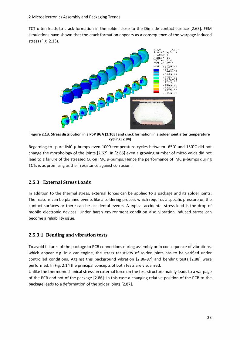
2 Microelectronics Assembly and Packaging Trends
23
TCT often leads to crack formation in the solder close to the Die side contact surface [2.65]. FEM
simulations have shown that the crack formation appears as a consequence of the warpage induced
stress (Fig. 2.13).
Figure 2.13: Stress distribution in a PoP BGA [2.105] and crack formation in a solder joint after temperature
cycling [2.84]
Regarding to pure IMC µ-bumps even 1000 temperature cycles between -65°C and 150°C did not
change the morphology of the joints [2.67]. In [2.85] even a growing number of micro voids did not
lead to a failure of the stressed Cu-Sn IMC µ-bumps. Hence the performance of IMC µ-bumps during
TCTs is as promising as their resistance against corrosion.
2.5.3 External Stress Loads In addition to the thermal stress, external forces can be applied to a package and its solder joints.
The reasons can be planned events like a soldering process which requires a specific pressure on the
contact surfaces or there can be accidental events. A typical accidental stress load is the drop of
mobile electronic devices. Under harsh environment condition also vibration induced stress can
become a reliability issue.
2.5.3.1 Bending and vibration tests
To avoid failures of the package to PCB connections during assembly or in consequence of vibrations,
which appear e.g. in a car engine, the stress resistivity of solder joints has to be verified under
controlled conditions. Against this background vibration [2.86-87] and bending tests [2.88] were
performed. In Fig. 2.14 the principal concepts of both tests are visualized.
Unlike the thermomechanical stress an external force on the test structure mainly leads to a warpage
of the PCB and not of the package [2.86]. In this case a changing relative position of the PCB to the
package leads to a deformation of the solder joints [2.87].

2 Microelectronics Assembly and Packaging Trends
24
Figure 2.14: Principal experimental setup of bending (a) and vibration tests (b) in [2.86] and [2.87]
In [2.86] vibration tests were performed at cycling frequencies between 10Hz and 27Hz, afterwards
finite element simulations were made to extend the frequency range (0.001-3450Hz). Independent
from the chosen frequency the crack formation mainly appeared in the bulk solder [2.86-87]. Curve
fitting showed a good correlation between the test results and the Basquin equation (2.17) [2.86].
Hence plastic deformation is the main reason for the fatigue of the solder joints during vibration
testing.
While the thermal stress was coupled with the CTE, the stress amplitude during the vibration test
depends on the angular acceleration (\ ), the mass of the test structure (“M” e.g. package + PCB +
additional weight), the distance from the package to the tester (L) and the contact surface (A) [2.86]:
; =S\ )⁄ 2.18 Bending tests being performed with a 3Hz cycle rate show a similar correlation between the strain
amplitude and the cycle lifetime as the vibration test results [2.87-88].
2.5.3.2 Drop tests A drop test means that a PCB with one or several packages is mounted on a metal weight which will
be dropped on a target (Fig 2.15). Drop tests are necessary to evaluate the influence of mechanical
shocks on the package reliability. When the metal weight smashes on the target an impulse goes
through the PCB and the packages [2.89]. First the breaking force bends the PCB and afterwards a
stress wave is going through the devices (e.g. with 245Hz) [2.89]. Because of the fact that the PCB is
much more deformed than the package, the PCB has to be standardized to get reproducible and
comparable test results [2.89]. A typical break force for consumer products is F~1500gn*M [2.90],
while reliability tests for harsh environment applications go up to F~10000gn*M. For future harsh
environment applications and military application also F~100000gn*M will be required.
From the first point of view a drop test is a combination of a bending and a vibration test, but due to
the huge brake force during the impact of the tested device, high strain rates appear at the solder
joints [2.89].

2 Microelectronics Assembly and Packaging Trends
25
Figure 2.15: Principal procedure for a drop test
Two typical failure pictures after TCT and drop tests on lead free solder bumps are shown in Fig. 2.16
[2.88]. Failure analysis has shown that the crack formation during drop tests often appears at the
interface between solder and IMC or in the IMC [2.88-92].
Figure 2.16: Crack formation in the solder during TCT (left), and crack formation in the IMC layer during drop
tests (right) [2.88]
In principal the deformation profile of the solder joints during the drop tests is similar to vibration or
bending test results, but drop tests show a different strain to cycle lifetime correlation (Fig. 2.17)
[2.87]. This is a clear indicator that a new failure mechanism appeared during the drop tests.
Figure 2.17: Cycles to failure vs. Board strain for vibration, bending and shock tests (left) [2.87], relative UTS
of SnAgCu and Cu-Sn IMCs at different strain rates (right) [Data: 2.93-94]
The different failures after low cycling fatigue tests (bending, vibration) or drop tests are due to the
different strain rate sensibilities of solders and IMCs [2.92]. In the case of low strain rates the
ultimate tensile strength (UTS) of solders is lower than the UTS of IMCs, but the solders are more
strain rate sensitive than the IMCs. Hence at a high strain rate, which appears during drop tests, the
UTS of the solders is greater than the UTS of the IMCs (Fig. 2.17). That means if the strain rate is high
enough the IMC becomes more fragile than the solder and the crack formation appears in the IMC. In
[2.95] it was also clarified that the crack formation often appears at the interface between the two
Cu-Sn IMCs Cu6Sn5 and Cu3Sn. Hence a weak interface between the IMCs may be more important for
the drop test reliability than the UTS of the IMCs [2.95].

2 Microelectronics Assembly and Packaging Trends
26
The main failure mechanism during drop tests as well as for bending or vibration tests is the warpage
of the PCB [2.90]. The bending wave going through the PCB is described by (2.19) [2.89] and the
maximum deformation (umax) of the board is given by (2.20). The maximum deformation of the board
depends on the fall velocity (v) which can be calculated with (2.21) when the aerodynamic resistance
is negligible.
<4L12 ∙ ?^_?_ (, ) + ?^
? (, ) = 0 (2.19)
^YEH = `24 <⁄ ∙ aS bc d ∙ e ℎLc (2.20) e = `2"[ (2.21)
ρ= mass density; lB= board length; g= acceleration; H= drop height
In general the performance of the test structure depends on the test conditions like the drop height
(velocity) or the direction of fall [2.96], the test device (board dimensions) and the shape and number
of the solder joints. It was shown that a higher number of solder joints increase the drop test
performance asymptotically to an upper limit while a decreasing contact surface adulterates the drop
test performance [2.89]. The influence of the board thickness is more complex, a thin board
increases the maximum warpage of the PCB, but a too thick PCB can also lead to a high stiffness of
the test structure, which would increase the break force [2.89]. Investigations by T. Matilla [2.97]
have shown that TCT before the drop testing improves the drop test performance of solder joints
due to annealing, but diffusion processes during temperature cycling also lead to the formation of
Kirkendall voids in the IMCs, which reduces the robustness of the solder joints when their number
becomes too high [2.97-98].
In difference to corrosion or electromigration induced reliability issues, solder bumps on Ni pads
have a reduced drop test performance compared to solder joints being directly connected to the
metal lines [2.90, 2.98]. The reduced performance is due to the Ni content in the Cu6Sn5 IMC layer,
because Ni increases the stiffness of Cu6Sn5 [2.83, 2.99].
2.5.4 Electromigration
Electromigration (EM) is a thermally activated diffusion process with a preferred direction being
defined by the momentum exchange between an electron flux and the diffusing lattice ions [2.10]. In
a few cases the electrical field defines the direction of the mass flux instead of the electron flux.
More details about electromigration and other diffusion processes in solids will be given in chapter 3
as the theoretical basis of the experimental procedure. Furthermore excellent overviews of migration
processes in general is given by Paul Shewmon [2.39] and Hans Wever [2.100].
After a period of time an electromigration induced mass flux leads to material degradation on one
side of the interconnect (anode/cathode) and a materials accumulation at the opposite side
(cathode/anode). Material accumulation can lead to hillock formation and finally to short circuits,
especially when two EM stressed structures are placed close to each other. Material degradation
leads to EM driven void formation and a disruption of the electrical contact. In general void
formation is the main failure mode.
The void formation has to be in an advanced state before a resistance increase appears [2.10, 2.101],
furthermore the accumulation of material on the opposite side of the stress can motivate a back flux
due to an increasing hydrostatic pressure (stressmigration) [2.102]. Hence the guaranteed lifetime
and the stressmigration induced back flux, also called “Blech Effect”, define a minimum current

2 Microelectronics Assembly and Packaging Trends
27
density (fYgh) where EM induced failures of electrical contacts are a relevant reliability issue. The
Blech effect depends on the length of the tested structure [2.102] and the maximum tensile stress of
the surrounding materials [2.103]. Electrical contacts also fail when void formation leads to
disruption before the volume of the displaced material is enough to establish a back flux being as
strong as the EM induced material transport [2.104].
On the IC level current densities in a range MA/cm² appear and the failure of Al or Cu interconnects
due to EM are a well-known problem since the 1960s [2.10]. Even under consideration of the rapid
down scaling due to three dimension packaging, the current density in solder bumps is several orders
of magnitude smaller than the current densities in IC interconnects (e.g. 1.1kA/cm² in [2.101] and
1.8kA/cm² in [2.65, 2.105]), but the low activation energies (melting point) of Sn solders compared to
Al or Cu lead to a high diffusivity of its lattice ions. In addition the relatively low melting point of Sn
means that the use condition of the chips (T<100°C) is much closer to the critical value, being 80% of
the material melting point, than for high melting metals like Cu or Al. Furthermore the big difference
between the metal layer and the solder bump contact surface leads to local peaks of the current
density (51kA/cm² in [2.101] and 3.6kA/cm² in [2.105]). The effect is called "current crowding" and it
is visualized in Fig 2.18 (left).
Figure 2.18: Formation of a pancake void and IMC growth as a consequence of electromigration and current
crowding (left), void in an electromigration stressed SnAgCu bump (right)
Following the JEDEC standard [2.106] the mean lifetime of solder joints under EM stress can be
approximated with the Black equation (2.22) [2.107], which is also used for interconnects.
MMO~jhk<J KLM⁄ 2.22 j= current density; nB= exponential constant
EM induced void or hillock formation is the consequence of a local difference of the mass flux
density. Using (2.23), being a more detailed model for the calculation of the EM induced mass flux
(lU-), it is possible to describe the EM influence on the material density by the divergence of the
resulting vector field [2.108]. Eq. (2.24) describes the mass flux divergence as a consequence of an
inhomogeneous temperature distribution.
lU- mnk o∗f fYgh Gq6<J KLM⁄ 2.23
N= atomic density; e= elementary charge; D0= diffusion constant; ρel = specific resistance;
Z*= effective charge of the moving ion
$re3lU-5 I <JKLM & M!s ∙ 1MN ∙ lU- ∙ "Rt$M 2.24

2 Microelectronics Assembly and Packaging Trends
28
Based on (2.24) an alternative interpolation of the expected TTF under EM stress is possible (2.25).
MMO~ 1 $re3lU-52.25 ⁄
Comparing (2.22) and (2.25) and taking into account that the temperature gradient, leading to a mass
flux divergence, can be the consequence of Joule heating (gradT~j2), the relation between “nB” in and
“j” in (2.22) becomes clear. In summary a mass flux divergence and the related void formation have
two possible reasons:
1. Void formation as a consequence of Joule heating being indicated by nB=3 in the Black equation:
nB=1 for Jvw and nB=2 for gradT due to Joule heating (~j2).
2. Material degradation at a diffusion barrier. In this case a “diffusion barrier” can be every material
with quite lower diffusivity than its neighbors (e.g. Cu next to Sn). This failure case is indicated by
nB=1 in the Black equation.
In solder joints both mechanisms are relevant for void formation. Hence the constant “n” is between
one and three [2.109-110]. If nB>3, the applied current changed one of the boundary conditions, e.g.
Joule heating significantly increased the test temperature (T), which would reduce the TTF
exponentially.
The weak point of (2.22) is that it only considers temperature gradients being the consequence of
Joule heating. This assumption is sufficient for interconnects. In case of IC packaging, and especially
for three dimensional packaging, the ICs act as hot spots leading to external temperature gradients
not being considered by the Black equation. As consequence the Black equation overestimates the
lifetime of solder joints for three dimensional packaging [2.31, 2.105]. The weak point of (2.24) is the
fact that it does not consider mass flux divergences due to local differences of the diffusivity.
In lead free solder bumps the EM induced void formation appears at the interface between the less
mobile IMC components and the more mobile solder (Fig. 2.19, right). As a consequence of current
crowding and the resulting temperature gradients an initial void is formed at one of the corners of
the contact surface (Fig 2.19, left) [2.65, 2.101]. The void formation moves the edge of the solder
joints and by the way the point where current crowding and the further void formation appears. The
result is a pancake void which finally leads to a failure of the solder bump (Fig. 2.18 right). The
dominance of current crowding induced void formation enables the determination of weak points in
the design of solder bumps and a comparison of different designs and technologies with (2.24) and
FEM analysis [2.105, 2.111-113].
Figure 2.19: Calculation of the mass flux divergence [2.105] with ANSYS® and a user developed routine
[2.108] (left), a failure picture of the related EM test (right) [2.65]

2 Microelectronics Assembly and Packaging Trends
29
The presence of IMCs in solder joints has an influence on the EM induced failure mechanisms in
solder joints. The reason for the void formation at the interface between the IMCs and the solder is
due to the low mobility of atoms in the IMCs compared to the solder [2.114]. Furthermore the
presence of an EM induced mass flux accelerates the IMC formation [2.65, 2.115-117]. Pure Cu-Sn or
Ni-Sn IMC solder joints are not affected by EM induced failures. Even under harsh test conditions
being far beyond the CSP bump test conditions no EM induced failures were observable [2.118-120].
The main reason for the high EM performance of IMC solder joints is their relatively high activation
energy compared to Sn based solders [2.114].
2.6 Transient Liquid Phase Soldering The growing importance of IMCs due to the downscaling of solder joints and the use of
microelectronic devices under harsh environment conditions as well as the promising results of IMC
micro bumps in many aspects of microelectronic packing reliability show the great importance of
TLPS for future packaging techniques. Consequently the existing models for the design of a TLPS
process step will be explained and the required material parameters will be mentioned. Afterwards
the unavailability of valid material parameters will be shown.
2.6.1 Process Design TLPS is a diffusion driven soldering process which forms an IMC solder joint out of a low and a high
melting material. The TLPS process can be performed by melting the interlayer (SLID) or by solid
diffusion only (SMB). Furthermore a combination of both TLPS techniques is possible (SLID+SMB).
Based on [2.53, 2.121-122] the four principal process steps of TLPS are shown in Fig. 2.20:
1. Interlayer Widening: Melting of the interlayer. For a Cu-Sn IMC joint the interlayer would be Sn.
Due to high concentration gradients and the low activation energy of Cu in molten Sn (0.18-
0.29eV) [2.123] a fast dissolution of Cu in the interlayer appears.
2. Homogenization of the interlayer: Cu flows into the growing interlayer and the Cu content is
balanced on a low level.
3. Solidification: When the Cu concentration reaches a critical limit (mint) the melting point of the
interlayer is above the process temperature and a preliminarily IMC is formed. After the
formation of an IMC the further process flow depends on the solid state diffusivity of Sn and Cu
in this IMC.
4. Homogenization of the bond region: Cu and Sn still diffuse through the solid preliminary IMC
layer and form the favored IMCs with a higher Cu content (Cu6Sn5 or Cu3Sn). The solid state
diffusivity of Cu and Sn is three orders of magnitude lower than their diffusivity in liquid
materials [2.124]. As a consequence the fourth process steps needs more than 90% of the
process time.
In dependence of the chosen process temperature for step (4) the interlayer stays liquid (pure SLID)
or the process temperature is reduced and the IMC formation is driven by solid state diffusion
(SLID+SMB).

2 Microelectronics Assembly and Packaging Trends
30
Figure 2.20: The principal process steps of Transient Liquid Phase Soldering (s): solid; (l): liquid
The first two steps of TLPS only need a few minutes and their relatively high process temperatures,
being critical for many microelectronic devices, are also necessary for the realization of three
dimensional packaging solutions based the reflow of conventional tin solder BGAs. In [2.125] it is
shown that the Cu6Sn5 grows in scallops form on a flat surface of Cu3Sn. Over time the size of the
scallops increases, but their growing surface area is unfavorable and as consequence their number
decreases (Fig. 2.21). If the scallops get contact before the complete interlayer is molten void
formation appears and the final solder joints are brittle [2.126]. This defines the minimum thickness
of the Sn interlayer.
Figure 2.21: Formation of IMC scallops in SnPb at 200°C for 10s (a), 40 min (b) [2.125]
The third and the fourth steps are more critical because the following IMC formation is driven by
solid state diffusion and the mass flux is dramatically reduced compared to the first two steps. A too
high process temperature could destroy the microelectronic devices and consequently several hours
are needed to form the final IMC connection [2.53, 2.115]. Against this background it can be
reasonable to reduce the process temperature of the fourth step and change from SLID to SMB.
Taken into account that the bottleneck during SLID is given by the solid IMC layer, the pure solid
state diffusion during SMB does not affect the total process time too much. Furthermore the SMB
process can be accelerated with a mass flux due to electromigration (lU-) and thermomigration
(l-). This can be done by combining the temperature storage step with a high applied current

2 Microelectronics Assembly and Packaging Trends
31
directly leading to EM and indirectly leading to TM as consequence of Joule heating. Hence the
benefits of “SLID+SMB” are a lower process temperature and the possibility to accelerate the process
with EM and TM. In fact reflow soldering being combined with the down scaling of the solder joints is
nothing else than SLID, so the conventional process flow does not have to be changed (low operation
barrier).
In [2.53, 2.121] a mathematical model for the process design of a SLID process is given: The first
process step is driven by diffusion and only needs a few seconds, like for moisture diffusion, Fick’s
law (2.10) can be used to describe the mass flux over time. The following three steps of the SLID
process are too complex for a theoretical description and consequently the power law (2.26) is used
to approximate the IMC thickness over time.
4 tx ∙ hy (2.26)
aP= pre exponential constant, nP= exponential constant.
The power law is only empirical and significant failures during the calculation of the process time can
appear. Taking into account that the IMC formation is driven by diffusion only and that the involved
materials have to pass the IMC layer the Deal-Grove model [2.127] can be used to describe the IMC
growth (Eq. 2.27). This model includes a linear part and a root function. For short process time a
linear growth of the IMC can be expected and for a long process times the square root curve
becomes more relevant. Comparing (2.26) and (2.27) leads to the conclusion that “n” depends on the
process time and should be 0.5<n<1.
ℎ() = − z2 + `z + 4o ∙ 2 ( > 0) ∧ (ℎ > 0) (2.27)
Y, ZG = constants
While the first two process steps only need a few minutes, the following process steps need several
hours, so they are most relevant for calculation of the total process time. In [2.53] a growth
approximation of the required process time in dependence of the diffusivity and the interlayer
thickness is given (2.28). Due to the difficulties to describe the third process step the calculated
process duration is several times longer than really required [2.53].
= ℎYEH b166~ ∙ I 1 − gh1 − ,-.N ∙ (<J KLM⁄ ) (2.28)
m= mass fraction
The Eq. (2.28) is not exact enough for the calculation of the process time but it allows an
interpretation of the expected IMC formation speed:
1. The final dimension (hmax) of the IMC solder joint has a strong influence on the process time. This
is relevant for high power or harsh environment applications with thick bonding layers.
If the solder joints are scaled down for high performance electronics it is more relevant that the
thickness of the interlayer has to be above a critical minimum. It is dictated by the used
temperature ramp [2.126].
2. A high maximum Cu concentration of the liquid interlayer (mint) reduces the process time.
Regarding to the phase diagram (Fig. 2.22) the maximum Cu concentration in the interlayer can
be increased with the process temperature, but this also means a higher stress load on the
microelectronic devices.

2 Microelectronics Assembly and Packaging Trends
32
3. The minimum Cu concentration of the final IMC (mIMC) is also relevant. Hence the fabrication of
a Cu3Sn or even a Cu41Sn11 IMC joint needs more time than the fabrication of Cu6Sn5 solder joints
[2.126]. Nevertheless Cu3Sn is more resistant against corrosion and electromigration than Cu6Sn5
and the relation between the process and the maximum operation temperature is better for
Cu3Sn than for Cu6Sn5 joints (Fig. 2.8).
4. The mobility of Cu and Sn in the IMCs has a very strong (exponential) influence on the process
time. Hence the process temperature and the activation energy of the materials have to be well
known before the process design is possible.
Figure 2.22: Cu-Sn phase diagram, the red line denotes a possible process temperature of 250°C [2.151]
In the case of an additional SMB step the process design has to take into account that the further
IMC growth appears due to solid state diffusion. The IMC growth due to solid state diffusion is
described by the Deal Grove model (2.27) or approximated by a square root curve as special case of
the power law [2.53, 2.115]: (2.26) with n=0.5. The IMC growth due to electro- or thermomigration
appears due to a drift of the diffusion induced mass flux and the IMC growth speed is linear time
dependent: (2.26) with n=1 [2.115].
In [2.115-117] investigations of the IMC growth during temperature storage and under the influence
of electromigration were made. In [2.115] also an illustration of the IMC formation process is given
(Fig. 2.23).
Figure 2.23: Concentration profile of a Cu on Sn contact with IMCs (a), the principal direction of the Cu and Sn
mass flux in the IMCs (b) [2.115]

2 Microelectronics Assembly and Packaging Trends
33
Before a mass flux can lead the formation of new IMC material its minimum concentration of Cu has
to be reached, hence the concentration difference between the previous and the new IMC (NCu3Sn,min-
NCu6Sn5,max or NCu6Sn5,min-NSAC) has to be overcome by the mass flux. In addition the driving forces, like
the concentration gradients, which transport material into the IMC, also transport material out of the
IMC (Fig. 2.23, right). Taken into account the presence of diffusion, electro- and thermomigration,
the general expression for the IMC growth speed in solids is be given by (2.29a-b)
e.2h 3lU- & l- & l5. 3lU- & l- & l5.h 3.,Ygh − .2h,YEH5 (2.29t)
e.h = 3lU- + l- + l5.2h − 3lU- + l- + l5J. 3.2h,Ygh − .h,YEH5 (2.29')
The required material parameters for a TLPS process design can be identified with (2.29a) and
(2.29b). The mass flux due to electromigration is described by (2.23), the mass flux due to
thermomigration can be calculated with (2.30) and the mass flux due to diffusion is given by (2.31).
l- = − ∗6KLM ∙ (− <J KLM⁄ ) ∙ "Rt$M (2.30)
l = −6 ∙ (− <J KLM⁄ ) ∙ "Rt$ (2.31)
Hence the following parameters will be needed for calculation of the migration induced movement
of Cu and Sn in Cu3Sn and Cu6Sn5.
Parameter Class Principal Sources
Specific resistance (ρel) Material Parameter Literature
Activation Energy (EA) Material Parameter, Diffusion Literature, Experimental*
Diffusion Constant (D0) Material Parameter, Diffusion Literature, Experimental*
Effective Charge (Z*) Material Parameter, Drift Literature, Experimental*
Heat of transport (Q*) Material Parameter ,Drift Experimental*
Concentration (N) Material Parameter Experimental*
Concentration Gradient Boundary Condition Experimental*
Temperature (T) Boundary Condition Experimental*, FEM**
Current Density () Boundary Condition Experimental*, FEM** Table 2.2: Material parameter and boundary conditions for the assumption of the TLPS process time.
* Experimental means own experimental results being presented in this work.
**FEM means results of ANSYS® simulations being performed during this work.
2.6.2 Available Material Parameters
During the last years several investigations on the IMC formation in different solders like SnPb or in
pure Sn were made. In general two different kinds of interconnects were used for the experimental
studies: direct solder to Cu connections without any interlayer and solder connects with a Ni
interlayer as diffusion barrier. Both are affected by IMC formation, but the migration mechanisms
and the composition of the IMCs are different (Fig. 2.24). Against this background the available
results of previous investigations will be given in two separate sections.
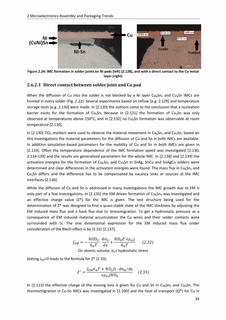
2 Microelectronics Assembly and Packaging Trends
34
Figure 2.24: IMC formation in solder joints on Ni pads (left) [2.128], and with a direct contact to the Cu metal
layer (right)
2.6.2.1 Direct contact between solder joint and Cu pad When the diffusion of Cu into the solder is not blocked by a Ni layer Cu6Sn5 and Cu3Sn IMCs are
formed in every solder (Fig. 2.22). Several experiments based on reflow [e.g. 2.129] and temperature
storage tests [e.g. 2.130] were made. In [2.130] the authors come to the conclusion that a nucleation
barrier exists for the formation of Cu3Sn, because in [2.131] the formation of Cu3Sn was only
observed at temperatures above 150°C, and in [2.132] no Cu3Sn formation was observable at room
temperature [2.130].
In [2.130] TiO2 markers were used to observe the material movement in Cu6Sn5 and Cu3Sn, based on
this investigations the material parameters for the diffusion of Cu and Sn in both IMCs are available.
In addition simulation-based parameters for the mobility of Cu and Sn in both IMCs are given in
[2.133]. Often the temperature dependence of the IMC formation speed was investigated [2.130,
2.134-139] and the results are generalized parameters for the whole IMC. In [2.138] and [2.139] the
activation energies for the formation of Cu6Sn5 and Cu3Sn in SnAg, SnCu and SnAgCu solders were
determined and clear differences in the activation energies were found. The mass flux in Cu6Sn5 and
Cu3Sn differs and the difference has to be compensated by vacancy sinks or sources at the IMC
interfaces [2.136].
While the diffusion of Cu and Sn is addressed in many investigations the IMC growth due to EM is
only part of a few investigations. In [2.135] the EM driven formation of Cu6Sn5 was investigated and
an effective charge value (Z*) for the IMC is given. The test structure being used for the
determination of Z* was designed to find a quasi-stable state of the IMC thickness by adjusting the
EM induced mass flux and a back flux due to stressmigration. To get a hydrostatic pressure as a
consequence of EM induced material accumulation the Cu wires and their solder contacts were
surrounded with Si. The one dimensional expression for the EM induced mass flux under
consideration of the Blech effect is by (2.32) [2.137].
lU- ΩDKLM ∙ $;$ & 6o∗GqjKLM 2.32
Ω= atomic volume, σH= hydrostatic stress
Setting JEM=0 leads to the formula for Z* (2.33).
o∗ lU-KLM & 6~Ω ∙ dσ dx⁄Gqj6 2.33
In [2.115] the effective charge of the moving ions is given for Cu and Sn in Cu6Sn5 and Cu3Sn. The
thermomigration in Cu-Sn IMCs was investigated in [2.100] and the heat of transport (Q*) for Cu in

2 Microelectronics Assembly and Packaging Trends
35
Cu3Sn was determined. Except for this value, the Q* for Cu and Sn is not available in the literature. All
material parameters are given in the tables 2.4 and 2.5.
Cu3Sn Cu Sn Cu3Sn Solder
EA [eV]
0.816 [2.133]
0.818 [2.130] -
0.894 [2.133]
0.827 [2.130] -
0.95 [2.138], 0.72 [2.139]
0.76 [2.130] 1.05 [2.138], 0.72 [2.139],
1.08 [2.138], 0.61 [2.139]
0.73 [2.138]
SnAg
Sn SnAgCu
SnCu
SnPb
D0 [m2/s]
2.21x10⁻⁶ [2.133]
1.8x10⁻⁸ [2.130]
2.49x10⁻⁶ [2.133]
7.9x10⁻¹⁰ [2.130]
5.63x10⁻⁷ [2.138]
2.7x10⁻⁹ [2.130]
5.95x10⁻⁶ [2.138]
1.09x10⁻⁵ [2.138]
1.85x10⁻⁹ [2.138]
SnAg
Sn
SnAgCu
SnCu
SnPb
Z* 26.6 [2.115] 23.6 [2.115] n.a. Sn
Q* [eV] -0.09 [2.100] n.a. n.a. Sn Table 2.3: Literature-available migration related material parameters for Cu3Sn. n.a.: not available
Cu6Sn5 Cu Sn Cu6Sn5 Solder
EA [eV]
0.835 [2.130] 0.88 [2.130] 0.84 [2.130]
0.75 [2.139]
0.93 [2.139]
Sn
SnCu/SnAgCu
SnAg
D0 [m2/s] 6.2x10⁻⁸ [2.130] 5.88x10⁻⁷ [2.130] 5.6x10⁻⁸ [2.130] Sn
Z* 26 [2.115] 36 [2.115] 68-87 [2.135]
Sn SnAgCu
Q* [eV] n.a. n.a. n.a. Table 2.4: Literature-available migration related material parameters for Cu6Sn5. n.a.: not available
The separate activation energies (EA) for the diffusion of Cu and Sn in Cu6Sn5 and Cu3Sn were found
to be 0.8eV, but the melting temperature of Cu6Sn5 (415°C) is lower than the melting temperature of
Cu3Sn (676°C). The melting temperature is directly related to EA [2.100]. Consequently the EA for the
motion of Cu and Sn in Cu6Sn5 should be lower than the EA of both elements in Cu3Sn, but previous
experiments do not show a difference (EA tables 2.4 and 2.5). Furthermore the given diffusion
constants (D0) of Cu and Sn in Cu3Sn differ by several orders of magnitude.
Especially for Cu the given Z* values are close to the nuclear charge. The values of Z* are the res ult
of the interaction between the atom nucleus and the electrical field and the interaction between the
surrounding electron gas and the electron wind due to the current flow. Therefore the given values
for Z* are relatively high. These high values are given without an explanation of transport
mechanisms in the Cu-Sn IMCs and it becomes clear that the mechanisms of migration in Cu-Sn IMCs
are not well understood to day.
This has the consequence that the EA, the D0 and the Z* of the moving ions have to be clarified for
both Cu-Sn IMCs. Furthermore the thermomigration in the Cu-Sn IMCs has to be investigated and Q*
values have to be extracted.

2 Microelectronics Assembly and Packaging Trends
36
2.6.2.2 Solder joints on ENIG pads When the Cu pads are covered with Ni the diffusion of Cu into solder joints is blocked and replaced
by the diffusion of Ni. The presence of Ni in the solder can lead to the formation Ni3Sn4 [2.137], but
this depends on the Cu content of the solder. Often the Ni layer is protected with a thin Au film that
leads to the formation of Au4Sn during reflow [2.137].
In [2.140] it is shown that the presence of the Cu suppresses the formation of Ni-Sn IMCs during
temperature storage by reducing the consumption rate of Ni. In [2.141] a SnAg solder joint without
Cu content was temperature stressed and the formation of Ni3Sn4 was observed. In the following EM
tests the growth speed of Ni3Sn4 was reduced by electromigration without any difference between
up- and downstream cases. The missing influence of the current direction was explained by an
opposite direction of the material exchange between Ni and Sn at the cathode and anode sides . A
thermomigration induced formation of Ni3Sn4 in SnAg micro-bumps was proven in [2.142]. It was also
shown that the Ni3Sn4 formation is suppressed below a critical temperature gradient. This critical
temperature gradient decreases rapidly for smaller bump heights.
In [2.143] EM tests with SnAgCu solders were performed: if temperature storage is combined with an
applied current Ni3Sn4 is formed in SnAgCu. In contrast with [2.141] a clear difference of the IMC
thickness was found for up- and downstream tests, this is a clear indication for an EM induced mass
flux. The only visible difference between both investigations is the use of SnAgCu in [2.143] instead of
SnAg while the current density was similar and the test temperature was even a little bit lower than
in [2.141]. Hence the presence of a current flow is necessary to form Ni3Sn4 in SnAgCu, but the
presence of a relevant EM induced mass flux or its influence on the IMC formation is not clear.
Overall only a few material parameters for the migration induced Ni3Sn4 formation are available
(Table 2.5). There is a wide range of possible activation energies and no values for SnAgCu are
available. The effective charge values in [2.144] decrease with a rising test temperature which
indicates that the used activation energy of 1.2eV is too high. Furthermore stress tests with
alternating current are necessary to suppress a directed mass flux due to EM and to show a possible
electrochemical reaction between SAC and Ni as a consequence of an electron flow. A possible Q*
value of Ni3Sn4 is mentioned in [2.142] without further explanation.
Ni Sn Ni3Sn4 Solder
EA [eV] n.a. n.a.
0.75 [2.145]
0.56 [2.147]
0.94 [2.148]
0.99 [2.146]
1.14 [2.149] 1.21 [2.144]
SnAg
SnAg
SnAg
Sn
SnAg SnAg
D0 [m2/s] n.a. n.a. n.a.
Z* n.a. n.a. -160 to (-60) [2.144] SnAg
Q* [eV] n.a. n.a. 0.08? [2.142] SnAg Table 2.5 Literature-available migration related material parameters for the Ni3Sn4 in SnAg. n.a.: not
available

2 Microelectronics Assembly and Packaging Trends
37
2.7 Conclusion
On the permanently changing market for microelectronic products the creation of innovations is a
must. The performance of a new product being related to concepts like “More Moore” or “Beyond
Moore” is important, but not the only relevant factor. In addition the costs and the risks of
development on the company’s side, as well as the benefits and the financial risks on the customer’s
side have to be taken into account. The realization of “More Moore” or “Beyond Moore”, by
downscaling on transistor level or by the creation of new transistor technologies, is coupled with
exponentially increasing costs for the equipment and increasing development risks due to quantum
mechanical effects and the growing relevance of the signal transit time for the final clock rate.
Against the background of limited financial resources, alternative concepts like “More than Moore”
were developed to drive innovations on the microelectronic market. One idea of “More than Moore”
is to replace the downscaling on transistor level by the three dimensional packing of ICs. Furthermore
the use of existing microelectronic devices under harsh environment conditions develops new
markets for the semiconductor industry. By that way the “More than Moore” concept enables the
manufacturers to be in touch with their customers’ needs and it keeps the costs and development
risks under control.
A critical consequence of three dimensional packaging is a growing number of electrical contacts per
package. A growing number of solder joints in a BGA becomes possible by downscaling of the bump
diameter. Unfortunately the reduced dimension of the solder joints means that the current density is
increased. As a consequence low melting solders like SnAgCu or SnPb are affected by EM induced
reliability issues. In addition the melting point of Sn based solders is too low for harsh environment
applications. Hence alternatives to the conventional reflow soldering with low melting materials have
to be developed.
Compared to different alternatives to reflow soldering the transformation of conventional solder
joints into IMC joints is a promising concept. IMCs like Cu6Sn5 and Cu3Sn have a higher melting point
than Sn based solders and a lower melting point than Cu. Hence the transformation of Sn based
solder joints into IMC joints can be performed at relatively low process temperatures, while the
maximum operation temperature of the final IMC joints is relatively high. In addition Cu-Sn IMC
bumps have shown very promising results in all aspects of IC packaging reliability.
The diffusion and migration driven transformation of Sn based solder joints into IMC joints is called
Transient Liquid Phase Soldering (TLPS). The process times of TLPS depend on the solid state diffusion
of Cu and Sn. A high process temperature clearly increases the IMC formation speed, but it also
induces high thermal stress values in the ICs. The presence of a current flow also accelerates the IMC
formation by inducing additional mass fluxes due to EM and TM. The benefit of an EM and TM
accelerated IMC formation is that the process temperature does not have to be increased.
Nevertheless for a prediction of the TLPS process time a general model of the diffusion and migration
driven IMC formation is needed.
Unfortunately the availability of valid material parameters for the modeling of diffusion and
migration driven IMC formation is in a stark contrast with the relevance of TLPS. Hence for the
required prediction of the IMC formation speed the diffusion, EM and TM related material
parameters have to be determined by our own experiments.
3 Theory of Diffusion and the Experimental Setup
38
3 Theory of Diffusion and the Experimental Setup
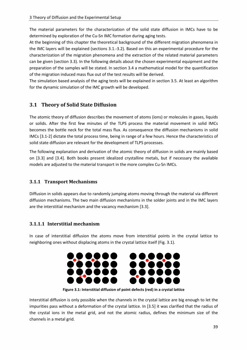
3 Theory of Diffusion and the Experimental Setup
39
The material parameters for the characterization of the solid state diffusion in IMCs have to be
determined by exploration of the Cu-Sn IMC formation during aging tests.
At the beginning of this chapter the theoretical background of the different migration phenomena in
the IMC layers will be explained (sections 3.1.-3.2). Based on this an experimental procedure for the
characterization of the migration phenomena and the extraction of the related material parameters
can be given (section 3.3). In the following details about the chosen experimental equipment and the
preparation of the samples will be stated. In section 3.4 a mathematical model for the quantification
of the migration induced mass flux out of the test results will be derived.
The simulation based analysis of the aging tests will be explained in section 3.5. At least an algorithm
for the dynamic simulation of the IMC growth will be developed.
3.1 Theory of Solid State Diffusion
The atomic theory of diffusion describes the movement of atoms (ions) or molecules in gases, liquids
or solids. After the first few minutes of the TLPS process the material movement in solid IMCs
becomes the bottle neck for the total mass flux. As consequence the diffusion mechanisms in solid
IMCs [3.1-2] dictate the total process time, being in range of a few hours. Hence the characteristics of
solid state diffusion are relevant for the development of TLPS processes.
The following explanation and derivation of the atomic theory of diffusion in solids are mainly based
on [3.3] and [3.4]. Both books present idealized crystalline metals, but if necessary the available
models are adjusted to the material transport in the more complex Cu-Sn IMCs.
3.1.1 Transport Mechanisms
Diffusion in solids appears due to randomly jumping atoms moving through the material via different
diffusion mechanisms. The two main diffusion mechanisms in the solder joints and in the IMC layers
are the interstitial mechanism and the vacancy mechanism [3.3].
3.1.1.1 Interstitial mechanism
In case of interstitial diffusion the atoms move from interstitial points in the crystal lattice to
neighboring ones without displacing atoms in the crystal lattice itself (Fig. 3.1).
Figure 3.1: Interstitial diffusion of point defects (red) in a crystal lattice
Interstitial diffusion is only possible when the channels in the crystal lattice are big enough to let the
impurities pass without a deformation of the crystal lattice. In [3.5] it was clarified that the radius of
the crystal ions in the metal grid, and not the atomic radius, defines the minimum size of the
channels in a metal grid.
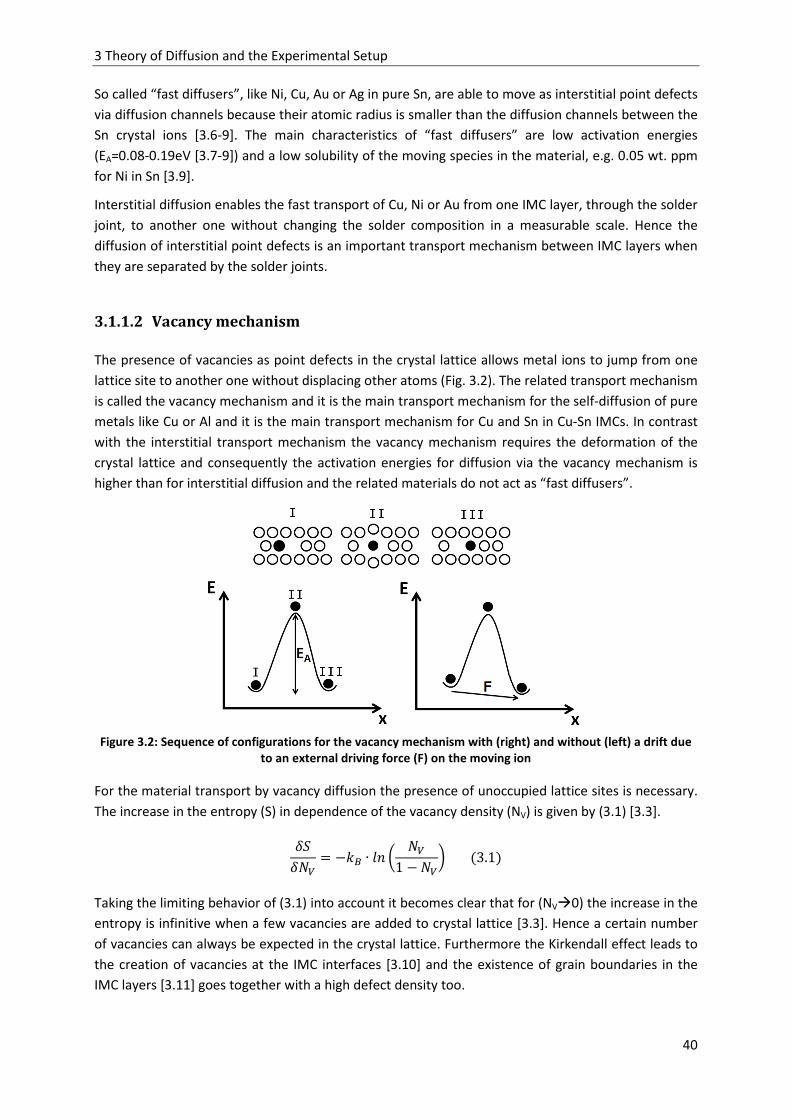
3 Theory of Diffusion and the Experimental Setup
40
So called “fast diffusers”, like Ni, Cu, Au or Ag in pure Sn, are able to move as interstitial point defects
via diffusion channels because their atomic radius is smaller than the diffusion channels between the
Sn crystal ions [3.6-9]. The main characteristics of “fast diffusers” are low activation energies
(EA=0.08-0.19eV [3.7-9]) and a low solubility of the moving species in the material, e.g. 0.05 wt. ppm
for Ni in Sn [3.9].
Interstitial diffusion enables the fast transport of Cu, Ni or Au from one IMC layer, through the solder
joint, to another one without changing the solder composition in a measurable scale. Hence the
diffusion of interstitial point defects is an important transport mechanism between IMC layers when
they are separated by the solder joints.
3.1.1.2 Vacancy mechanism
The presence of vacancies as point defects in the crystal lattice allows metal ions to jump from one
lattice site to another one without displacing other atoms (Fig. 3.2). The related transport mechanism
is called the vacancy mechanism and it is the main transport mechanism for the self-diffusion of pure
metals like Cu or Al and it is the main transport mechanism for Cu and Sn in Cu-Sn IMCs. In contrast
with the interstitial transport mechanism the vacancy mechanism requires the deformation of the
crystal lattice and consequently the activation energies for diffusion via the vacancy mechanism is
higher than for interstitial diffusion and the related materials do not act as “fast diffusers”.
Figure 3.2: Sequence of configurations for the vacancy mechanism with (right) and without (left) a drift due
to an external driving force (F) on the moving ion
For the material transport by vacancy diffusion the presence of unoccupied lattice sites is necessary.
The increase in the entropy (S) in dependence of the vacancy density (NV) is given by (3.1) [3.3].
KL ∙ S I 1 N 3.1
Taking the limiting behavior of (3.1) into account it becomes clear that for (NV0) the increase in the
entropy is infinitive when a few vacancies are added to crystal lattice [3.3]. Hence a certain number
of vacancies can always be expected in the crystal lattice. Furthermore the Kirkendall effect leads to
the creation of vacancies at the IMC interfaces [3.10] and the existence of grain boundaries in the
IMC layers [3.11] goes together with a high defect density too.

3 Theory of Diffusion and the Experimental Setup
41
3.1.2 The Random Walk Problem and the Diffusion Coefficient For the interstitial and for the vacancy mechanism the effective motion of the atoms can be defined
as a “Random Walk Problem”. This is due to the fact that the atoms in a crystal lattice are jumping
randomly from one lattice site to a neighboring one. Random walk means: even when no preferred
direction is given a certain number of atoms passes an average distance over time (Fig. 3.3)
Figure 3.3: Initial distribution of atoms (left), and distribution of atoms after a few jumps (right)
This phenomenon was observed in macroscopic particles in 1827 by Robert Brown and was later
called “Brownian Motion”. Based on the “Random Walk Problem”, which was firstly described by Karl
Pearson in 1865 [3.12], Albert Einstein developed an atomistic theory of Brownian motion in 1905
[3.13]. The following description of the model is based on the root-mean–square displacement (s)
of many atoms after many possible jumps (n) and the following assumptions:
1. The passed distance per jump (R) will always be the same, which would be correct for a face
centered cubic (fcc) crystal structure.
2. For every lattice site an atom could jump to, there will be another free lattice site in the
opposite direction. The jumping probability in both directions will be the same (Rg R).
3. The process is completely randomized, hence it has no a preferred direction. This is correct
when no driving force leads to drift of the atomic movement (Fig. 3.2).
The average distance being passed by the atoms over time (t) can be described as a sum of “n”
vectors (3.2). The number “n” is the jumping frequency of the atoms (f) multiplied with the time
(3.3).
sh R & R & R2 … Rh Rgh
g3.2 ∙ 3.3
The value of the vector sh is given by (3.4) [3.3 p. 62]:
sh ∙ sh sh Rgh
g∙ Rg & 2 ∙ Rg ∙
h
g
h
Rg Rg
h
g& 2 ∙ |Rg| ∙
h
g
h
Rg ∙ 3g,g53.4
Based on the assumption (1-3), with assumption (2) leading to cos (θi+j)=cos(θi)+/-180°, and taking
into account many jumps of many atoms (n>>1) Eq. 3.4 can be simplified to (3.5). In this case the
double summation becomes zero.

3 Theory of Diffusion and the Experimental Setup
42
sh ∙ R & 2R ∙ 3g,g5 ∙ R3.5 h
g
h
The diffusion coefficient (D) can now be defined by the root-mean–square displacement in on
direction (3.6). The diffusion coefficient depends on the jumping frequency of the atom and the
jumping distance. The factor 1/6 is due to the fact that the diffusion process appears in a three
dimensional system and two directions per dimension are available.
sh ∙ R 66 → 6 1 6⁄ ∙ ∙ R3.6 Material degradation due to diffusion is a reliability issue of IC interconnects being made of Cu or Al.
Both metals have a fcc crystal structure (Fig. 3.4) and assumptions (1-3) are sufficient. Nevertheless
even in this case the jumping frequency of the atoms is orders of magnitude smaller than their
vibration frequency (Debye frequency) [3.3]. Hence (3.6) cannot be used for the calculation of D with
common material parameters or the other way around. For the vacancy mechanism a reason for the
difference between the jumping and the Debye frequency is the fact that a vacancy has to be created
before the jump of a crystal ion is possible.
Figure 3.4: A unit cell with a face centered cubic -fcc- structure a=b=c (I), the unit cell of Cu6Sn5 (II) and the
superstructure of Cu3Sn (III) based on the CuTi3 unit cell [3.14]
The investigated Cu-Sn IMCs Cu6Sn5 and Cu3Sn have a more complex crystal structure than pure Cu or
Al (Fig. 3.4):
• The unit cell of Cu6Sn5 is based on two orthorhombic cells (a≠b≠c) with 12 Cu atoms at the regular
lattice sites and two base-centered Sn atoms with an alternating position (oB82) [3.14-15].
• The unit cell of Cu3Sn is a superstructure of 80 atoms being formed by a body-centered
orthorhombic structure of Sn atoms and Cu atoms with alternating positions on the structure
surfaces (oC80) [3.16-17].
In fcc crystals the distance between two lattice sites is always the same (r=a/2 in Eq. 3.6), but the
relatively complex crystal structure of IMCs leads to different jump distances in every direction and
as a consequence the diffusion coefficients of the IMCs are anisotropic. Furthermore the distance
between two neighboring lattice sites is different for Cu and Sn and the diffusion coefficients could
also be different.
On the other hand, if the motions of both elements seen as an interaction between two separate
crystal structures which form the IMC, the material exchange from one crystal structure to the other
should be equal. In this case the resulting diffusion constants of both elements in the IMCs would be

3 Theory of Diffusion and the Experimental Setup
43
similar [3.18]. Nevertheless this would require a vacancy mechanism leading to the replacement of
Cu sites by Sn, or the other way around, which would lead to a permanent deformation of the crystal
structure. Under these conditions the moving atoms should immediately jump back to their original
position to reduce configuration energy. Huntington mentioned the possibility of jumping cycles for
vacancies which would enable material transport as well as the rearrangement of the crystal
structure. Based on this assumption he described a vacancy mechanism based on a six jumps cycle
which described the material transport in binary alloys at low temperatures [3.18]. In the literature
similar [3.19] and very different diffusion coefficients [3.14] for Cu and Sn in Cu6Sn5 and Cu3Sn are
given, so it is not clear if a six jumps cycle or a simple vacancy mechanism is relevant for the material
transport in Cu-Sn IMCs.
Another problem which prevents the calculation of the diffusion constants for Cu-Sn IMCs with (3.6)
is the presence of grain boundaries as diffusion paths as shown in Fig. 3.5 [3.11], because their
amorphous structure disables the determination of a constant jumping distance. Overall the diffusion
coefficients of Cu and Sn in Cu6Sn5 and Cu3Sn have to be determined experimentally and the results
are empirical values being influenced by the anisotropy of the IMCs and the presence of grain
boundaries as diffusion paths.
Figure 3.5: Grain structure of Cu3Sn and Cu6Sn5 (left) and the amorphization of the crystal structure at the
grain boundaries (right) [3.11]
3.1.3 Derivation of the General Mass Flux Equation
Based on the solution of the random walk problem a general description of the migration induced
mass flux is possible. For the following description of the diffusion induced mass flux two planes in
the crystal will be defined (Fig. 3.6) and a vacancy transport mechanism will be supposed [3.3]. At
both planes a certain number of atoms will be present (nA [1/m²]). Every atom has a jumping
frequency “w” and for a successful jump to a neighboring lattice site a vacancy has to be created.
Hence the probability of a vacancy creation also has to be taken into account (pv). Finally the mass
flux at both surfaces is given by (3.7a-b).
l J ∙ ∙ ∙ $)3.7t l J ∙ ∙ ∙ $)3.7'

3 Theory of Diffusion and the Experimental Setup
44
Figure 3.6: Mass flux between two planes in a crystal lattice
For the further steps the following assumptions will be made:
1. The effective mass flux is defined by the difference between the mass flux from plane one to
plane two and the mass flux in the opposite direction: l l l.
2. The jumping frequency at both planes is the same w1=w2=w.
3. The vacancy formation probability at both planes is the same pV1=pV2=pV.
4. The planes are parallel to each other. The distance between both planes is t 3$) ∧ $)5.
5. The activity coefficient “K” is the probability that an atom jumps into the direction of +/-t. That
leads to Wand W.
6. If an external force (F) is present a drift of the diffusion induced mass flux appears because
K12≠K21, otherwise K12=K21.
Based on previous assumptions the resulting mass flux is now given by (3.8).
l ∙ ∙ W W ∙ t|t|3.8
With the volume density of the atoms 1/³ |t|⁄ , Eq. (3.8) can be transformed to (3.9).
l ∙ ∙ W W ∙ t3.9 With (3.10) the Eq. (3.9) can be transformed to (3.11), and additional theorems lead to (3.12).
W W t ∙ "Rt$W ∙ 3.10 l ∙ ∙ t ∙ "Rt$W ∙ 3.11
l ∙ ∙ t ∙ W ∙ "Rt$ & ∙ "Rt$W 3.12 Expecting a thermodynamic equilibrium, the Van`t Hoff equation [3.20] (3.13) with the
thermodynamic activity (G) (3.14) can be used to describe the chemical potential “μ” (change of
internal energy per atom). As solution the chemical potential (μ) is given in dependence of the
atomic density and the jumping probability “K“ (3.15).
∆¤ ¤ ¤ KL ∙ M ∙ ln§ 3.13 § ¨m©m© 3.14

3 Theory of Diffusion and the Experimental Setup
45
¤ ¤ & KLM ∙ S I WWN (3.15)
Taking into account the principals of thermodynamics, the mass flux should reduce the intrinsic
energy of the system. Hence the atoms have to follow the inverse direction of the chemical potential
gradients. The gradient of μ can be calculated out of (3.12) and algebraic functions lead to (3.16).
∙ WKLM ∙ "Rt$(¤) = W ∙ "Rt$() + ∙ "Rt$(W) (3.16)
Inserting (3.15) into (3.12) leads to the Nernst-Einstein equation (3.17). This step proves that the
Nernst-Einstein equation can be used for the calculation of the diffusion induced (F=0) as well as for
the calculation of the drift induced mass flux (F≠0). Hence the Nernst-Einstein equation enables the
physical interpretation of the test results in all possible cases.
l = − WtKLM ∙ "Rt$(¤) (3.17)
With |t| = |R| and = O (3.18) can be used to define D for the given system:
6 = W ∙ ∙ ∙ t (3.18)
At the moment (3.17) and (3.18) seem to be temperature independent, while (2.23), (2.30) and
(2.31) are exponentially temperature dependent. Furthermore (3.17-18) include parameters which
are difficult to measure, like the void formation probability or the jumping frequency of the atoms.
Hence it is necessary to describe a relation between these values and more basic material
parameters.
Expecting a thermodynamic equilibrium and referring to the Van`t Hoff equation the temperature
dependency of the void formation probability follows an Arrhenius relation [3.3] (3.19). In the same
manner the probability that an atom vibration leads to a jump from one lattice side to another one is
exponentially temperature dependent [3.3] (3.20).
= exp I−[KLM N (3.19) = e ∙ exp I−[YKLM N (3.20)
HV = Enthalpy change per vacancy added to an infinite crystal.
Hm= Enthalpy change per activated complex (intermediate state of an atomic interaction) added to
an infinite crystal.
vD= Debye frequency
Finally the activation energy (EA) needed for the movement of a crystal ion by the vacancy
mechanism is: EA=HV+Hm. Now D can be described by (3.21):
6 = W ∙ e ∙ t ∙ I− <JKLMN (3.21)
In addition to the EA the diffusion constant (D0) will be defined as the second temperature
independent material parameter to describe a migration induced mass flux. The D0 of a material
depends on the jumping distance, being related the lattice constant in the most simple cases, the
Debye frequency, and the probability that an atom jumps in the considered direction (3.22).

3 Theory of Diffusion and the Experimental Setup
46
6 W ∙ e ∙ t (3.22)
The final equations (3.23-24) describe the mass flux due to diffusion as well as due to the drift of
atoms as a function of the chemical potential gradient, the temperature and the generalized material
parameters EA and D0:
6 = 6 ∙ I− <JKLMN (3.23)
l = − 6KLM ∙ "Rt$(¤) ∙ I− <JKLMN (3.24)
Due to the complex crystal structure of the IMCs and the influence of diffusion paths, EA and D0 have
to be determined empirically. Nevertheless the given equations help to find experimental procedures
for the characterization of the migration processes and they enable the evaluation of the test results.
If the temperature difference between the two observed planes becomes relevant the void
formation probability (3.19) and the jumping frequency (3.20) of the atoms will not be equal
anymore. In this case the assumptions (2) and (3), which this derivation is based on, are not true
anymore. Under these conditions local mass flux divergences appear which change the material
density over time (2.24-25). The mass flux divergences are more relevant for reliability problems due
to the migration induced void formation than for the IMC formation. A detailed description of the
related mathematics is given in [3.21].
3.2 Specific Mass Flux Equations and Parameters The interpretation of the Nernst Einstein Equation leads to the following fact: if a gradient of the
chemical potential is present, the diffusion process has a preferred direction and a migration induced
mass flux appears. The mass flux goes in the reverse direction of the chemical potential gradient. The
identification of possible reasons for local differences of the chemical potential leads to the different
migration phenomena. The relevant reasons for a migration induced mass flux during the IMC
growth are:
1. concentration (N) gradients leading to the dissolution of an element in the solder joints,
2. an electric field/ an electron flux leading to electromigration,
3. temperature gradients leading to thermomigration,
4. and a difference in solubility of an element (e.g. the solubility of Cu in Cu-Sn IMCs and SnAgCu)
leading to local accumulation of this element.
Furthermore a gradient of the hydrostatic pressure can lead to stress migration, but this effect was
not found to be relevant for the IMC formation. Nevertheless the formation of Cu-Sn IMCs can lead
to high hydrostatic pressure in the solder joints [3.22-23].
The influence of the four relevant driving forces on the chemical potential leads to the mathematical
description of the related migration phenomena.

3 Theory of Diffusion and the Experimental Setup
47
3.2.1 Diffusion Expecting a concentration gradient without any additional influence on the jumping behavior of the
atoms (K=1) Eq. (3.15) can simplified to (3.25).
¤ ¤ & KLM ∙ S I N (3.25)
The gradient of the chemical potential is than given by (3.26):
"Rt$(¤) = KLM ∙ "Rt$() (3.26)
Inserting (3.26) into (3.24) leads to the mathematical description of the mass flux due to diffusion:
l = −6 ∙ "Rt$() ∙ I− <JKLMN (3.27)
Concentration gradients and the related diffusion processes will always be present in the IMC layers.
Hence in all experiments there will be an influence by diffusion and its characterization will be an
important step to prepare the following investigations of the other migration mechanisms.
3.2.2 Electro- and Stressmigration Electromigration (EM) is a thermally activated motion of atoms under the influence of a current flow.
EM is a well-known phenomenon in IC interconnects and often appears in combination with a back
flux by stressmigration. As a consequence of miniaturization EM has also appeared in solder joints.
3.2.2.1 Derivation of the mass flux equation Under the influence of an electric field the movement of ions changes their chemical potential if their
movement is directed with or against the field vectors. The chemical potential of a crystal ion in an
electrical field is given by the “effective charge of the moving ion” (eZ*) and the electrical potential
(Φ): ¤ = ∙ o∗¬ (3.28)
The gradient of the chemical potential is proportional to the gradient of the electrical potential. The
gradient of the electrical potential describes the electric field (<) and Ohms Law leads to a relation
between the current density and gradient of the chemical potential (3.29).
"Rt$(¤) = ∙ o∗"Rt$(¬) = − ∙ o∗ ∙ < = − ∙ o∗ ∙ Gq ∙ f (3.29)
The mass flux due to electromigration is given by (3.30/2.32).
lU- = 6 ∙ o∗fGqKLM ∙ I− <JKLMN (2.32/3.30)

3 Theory of Diffusion and the Experimental Setup
48
EM is often described by the statement that “electrons push the ions away from their lattice sites”.
Those statements are false because electromigration is a thermally activated mechanism because of
two reasons:
1. Respecting the fact that the maximum current density in a solid material is limited by Joule
heating, respectively its melting point, the gradient of the chemical potential of the moving ion
is much smaller than the activation energy (μ<<EA). In addition there is a big difference between
the mass and the resulting impulse of electrons and atoms.
2. A vacancy has to be created before diffusion is possible and the vacancy creation is thermally
activated (3.19).
In (2.23) the variable jmin is given as the minimum current density to cause electromigration. In (3.30)
this term is missing because it is related to a back flux due to stress migration called the Blech effect
[3.26]. A back flux appears when the mass flux due to EM leads to material accumulation at one side
of the test structure while the material density becomes lower at another one. The resulting
difference in the hydrostatic pressure (σH) leads to local stress gradients and a back flux due to the
stressmigration. The mass flux due to stressmigration can be described in the same way like the mass
flux due to EM.
The chemical potential of a single ion is given by its atomic volume (Ω) and the hydrostatic pressure
(3.31). The gradient of the chemical potential is than inserted into the Nernst-Einstein equation
which leads to the formula for the calculation of the back flux due stress migration (3.32).
¤ ∙ ; (3.31)
l- = −6 ∙ KLM ∙ "Rt$(;) ∙ I− <JKLMN (3.32)
In the following the minimum current density to cause EM is given by the equalization of (3.30) and
(3.32) ( f = fYgh):
fYgh = o∗Gq ∙ "Rt$(;) (3.33)
For the interpretation of (3.33) it is important to mention, that an EM induced elastic deformation of
the test structure is necessary to build up the hydrostatic pressure and the related stress gradients.
In case of interconnects for integrated circuits the deformation of the dielectrics and diffusion
barriers due to EM induced material accumulation leads to hydrostatic pressure and the related back
flux. As consequence the consideration of the Blech effect is a must for EM investigation on
interconnects. Nevertheless solder joints are often freestanding and no hydrostatic pressure and no
stress gradients can be created by EM. As result no Blech effect can appear in such solder joints (|fYgh| = 0).

3 Theory of Diffusion and the Experimental Setup
49
3.2.2.2 Interpretation of the effective charge of the moving ion (Z*) The determination of the effective charge of the moving ion (Z*) is one of the difficulties that have to
be overcome to describe the effect of EM on the IMC formation speed. In general the value of Z*
depends on the interaction between the electron flow (e-) and the electron shell of the metal ions
(OG). Furthermore the interaction between the electric field (<) and the atomic core (p+) has to be
taken into account (OV). As shown in Fig 3.7 the resulting driving forces have opposite directions.
Hence the difference of both driving forces leads to the effective driving force of the EM (O) and the
value of Z*. EM can follow the electron flux (Z*<0, e.g. Z*Cu=-5.5 [3.4]) or it can go into the direction
of the electric field (Z*>0 e.g. Z*Fe= 5.4 [3.4]).
Figure 3.7: Driving force (F) for electromigration, resulting from the difference between the electric field
force (Fp) and the momentum transfer due the electron flow (Fe), Z*>0
In pure metals the value of Z* should be bigger than the valence (Z) and smaller than the atomic
number. A mathematical definition of Z* based on physical parameters, like the effective electron
mass (me*), the defect density (ND) and the specific resistance of defects (ρD) is given by Huntington
[3.24].
o∗ o ∙ I12 ∙ GG∗ ∙ Gq,,YEH
Gq 1N 3.34 me= electron mass
In metals without a high defect density the effective charge is temperature independent [3.25]. In
IMCs the Kirkendall effect and the high number of grain boundaries lead to a strong influence of
vacancies on the electric field distribution. In the model of Bosvieux and Friedel [3.27] (3.35) the
vacancies are seen as an additive negative charge (–Ze) and the scattering of electrons at the crystal
defects is described by two Bessel functions (J0, J2). The resulting temperature dependent effective
charge value Z**(T) is the effective charge of a moving ion in a defective crystal lattice.
o∗∗ 12 ∙ o ∙ I1 ∙ ∙ N &
2® 3b o ∙ @l I tRN 2l I tRNC3.35 τ(T) = lifetime of the electrons, a = lattice constant, rH= Bohr radius
The temperature dependent effective charge value Z**(T) can be higher than the atomic number.
Often the Z**(T) values for EM in grain boundaries are higher than the bulk values (Z*) and the
direction of the mass flux changes: Z**Ag,GB=168, Z*Ag=-29 [3.4]. Hence the high defect density in the
IMCs could explain the relatively high Z* values in the literature (tables 2.3 and 2.4).

3 Theory of Diffusion and the Experimental Setup
50
3.2.3 Thermomigration A visual description of thermomigration (TM) is its definition as an alternative form of a heat flux
which is based on moving particles (e.g. atoms) instead of radiation (photons) or crystal vibrations
(phonons). Hence the mass flux due to TM should depend on the temperature gradients and the
moved thermal energy per atom.
3.2.3.1 Derivation of the mass flux equation The relation between the temperature and the chemical potential is relatively complex, because the
temperature has an influence on many other physical properties of the crystal lattice, like the lattice
vibration or the relation between volume and pressure.
The Euler equation describes the internal energy of a closed system (U) as the sum of energies (Ei)
being added to system by heat (Q) and work (W). The terms are given by the product of the volume
and the pressure (E=-W=-VP) and the product of the temperature and the entropy (Q=TS) (3.36). The
chemical potential is defined as the change of the internal energy per atom (3.37). The change of the
internal energy of a closed system can be described with the fundamental thermodynamic equation
(3.38).
¯ <g °g
M ∙ − F ∙ * (3.36) ¤ = $¯$ (3.37) ¤ ∙ $ = $¯ = M$ − F$* (3.38)
For the following step the term PdV will be supposed to be zero, because the volume change of solid
materials is negligible [3.28]. Furthermore many solder joints are free standing (P=0), and if a local
increase of the pressure (P σH<0) would appear, it would be removed by stressmigration:
$¯ = −F$* → ¤ = $*$ ∙ ; = Ω ∙ ; (3.39) → (3.31)
To determine the change of the chemical potential in dependence of the temperature change the
remaining terms of the fundamental thermodynamic equation are differentiated with respect to the
temperature (3.40). $¤ ∙ $ = $ ∙ $M (3.40) Taking into account the relation between the entropy change and the change of the thermal energy
(3.41), the chemical potential can be described by (3.42). TM is an alternative way to transport
thermal energy by the motion of crystal ions. Hence the material parameter to describe this effect
should be the thermal energy per ion. This parameter is called heat of transport (Q*=dQ/dN).
$ = $M (3.41) $¤ = $ ∙ $M$ ∙ M = ∗ ∙ $MM (3.42) The chemical potential at one lattice side, in dependence of the temperature, is that given by the
integration of (3.42) leading to (3.43). The gradient of the chemical potential as a consequence of a
temperature gradient is that given by (3.44).
¤ = ¤ + ∗S(M) (3.43)

3 Theory of Diffusion and the Experimental Setup
51
"Rt$¤ ∗M ∙ "Rt$M3.44
Inserting (3.44) into the Nernst Einstein equation (3.24) leads to the description of the mass flux due
to TM (3.45).
l- 6 ∙ Q∗
KLM ∙ "Rt$M ∙ I <JKLMN3.45
3.2.3.2 Interpretation of the heat of transport Q*
The characteristic parameter of the TM induced mass flux is the heat of transport Q*. An
interpretation of Q* is given by Wirtz (3.46) [3.3-4]: The value of Q* is given by the transport energy
of the moving ion HM, being multiplied with a factor βTM and subtracted by the vacancy formation at
the neighboring lattice side. The factor βTM is related to the interaction between the moving ion and
the crystal lattice during TM. The term HV can be interpreted as a thermal back flux of vacancies.
An illustration of the energy transmissions during the TM is given in Fig 3.8: to get the value of Q*,
the total amount of energy being transported per crystal ion (Hα), has to be reduced by the required
energy for the vacancy formation at the neighboring crystal site (HV). Furthermore the placement of
the ion at new lattice site needs a specific amount of energy too (Hγ). Hγ also has to be subtracted
from Hα. Often the difference between Hα and Hγ divided by HM can be interpreted as the factor βTM
(3.47).
∗ Q- ∙ [- [ 3.46 Q- 3[³ [´5 [-⁄ µ 0.83.47
Figure 3.8: Thermomigration by a vacancy mechanism; I: vacancy creation, II: mass flux, III: energy balance
Often the transported energy per crystal ion is close to the void formation energy, and the Q* values
are relatively small (e.g. Q*Cu=0.22eV [3.4]). Furthermore a material flux from the cold to the hot side
can appear if the void formation energy is bigger than the transported energy per crystal ion
(e.g. Q*Au= -0.22eV [3.4]).
In a solid compound like the investigated Cu-Sn IMCs the solubility of the elements is temperature
dependent. Hence the temperature gradients causing TM automatically lead to local differences in
the solubility. In this case the mass flux due to TM and a possible mass flux due to a temperature
induced difference in solubility have the same driving force and they cannot be separated
experimentally. Under these conditions a combined description of both effects is necessary. It was
given for binary alloys by Wever [3.4]. The model of Wever includes a term named the heat of
solution (HS). It describes the thermal energy being needed to solve or segregate an element of a
solid compound. With HS and an Arrhenius relation the temperature dependent maximum
concentration can be calculated (3.48). HS can be defined as an additional portion of transported

3 Theory of Diffusion and the Experimental Setup
52
thermal energy per ion. The resulting equation for the TM induced mass flux in a binary alloy is that
given by (3.49).
YEH ∙ I− [KLMN (3.48)
l- = −6 ∙ ∙ (Q∗ + H·)KLM ∙ "Rt$(M) ∙ I− <J + [KLM N (3.49)
For the interpretation of Q* through physical parameters Gerl divided it into two parts (3.50) [3.29].
One part describes the influence of lattice vibrations represented by phonons (Q*p) and one part
describes the influence of the electron gas (Q*e). The phonon’s influence on Q* was described by
Adolf Eugen Fick [3.4] (3.51). Nevertheless in metals the thermal transport is mainly done by the
electron gas.
∗ = V∗ + G∗ (3.50) V∗ = ;VeV ¸M (3.51)
σP= cross section for phonon scattering, vp= speed of sound, κ= thermal conductivity
The importance of the electron gas for the TM in metals indicates a relation between the effective
charge Z* and the heat of transport Q*. Gerl and Brebec [3.30] found a relation between Z* and Q*
for pure, fcc structured metals like Cu or Ag by ignoring the thermal electrical field and the electron
scattering at crystal defects (3.52).
G(¹∗,)∗ = − b6 ∙ (KLM)
Tº ∙ @1 + »?S;G(¹)?T ¼½½º
C ∙ o∗ (3.52)
ԑF= Fermi energy, σe= cross section for electron scattering
In the IMC layers the high defect density has to be taken into account. Based on the work of Bosvieux
and Friedel [3.27], Gerl developed a formula for the calculation of Q* under consideration of the
thermal electrical field (3.53) [3.29].
G(¹∗,)∗ = − G_`G∗√216bTℎx2 ∙ ¸GM
√Tº ∙ ;G(¹∗) ∙ @1 + 2 »?S;G(¹∗)?T ¼½½º
C (3.53)
hP=Planck’s constant, ε0= vacuum permittivity, κe= thermal conductivity by the electron gas
Like the model of Bosvieux and Friedel (3.35) the equation of Gerl can also be used for the
calculation of Q* under consideration of electron scattering at vacant crystal sites Q** (3.54) [3.29].
G(¹∗,)∗∗ = 12 ∙ »−o∗M + @1 + 2l(t R⁄ ) − l(t R⁄ )l(0) C ∙ G(¹∗,)∗ ¼ (3.54)
sT= thermoelectric voltage
The Eqs. (3.52) and (3.54) are not the easiest way to get Q* of Cu and Sn in Cu3Sn and Cu6Sn5, but the
relation between Q*and Z* enables the interpretation of the test results based on the following
statements:
1. Unlike the effective charge the heat of transport is temperature dependent (3.52), even when
no electron scattering at crystal defects is taken into account.

3 Theory of Diffusion and the Experimental Setup
53
2. When Z**(T) is increased due electron scattering, Q**(T) should also be increased. Investigations
on the thermomigration in Pb have shown an increased heat of transport for grain boundary
diffusion: Q**Pb,GB=0.25eV [3.31], Q*Pb=0.09eV [3.4]
3.2.4 Mass Fluxes due to Differences in Solubility During the IMC growth in solder joints the copper content in the in SnAgCu solder decreases with
increasing test time, while copper is accumulated in the IMCs [3.32]. In case of solder joints with Ni
pads as diffusion barriers no diffusion of Cu from the metal lines into the solder joints can appear and
the accumulation of Cu from the SnAgCu reservoir becomes important for the (CuNi)6Sn5 formation
[3.33]. Furthermore it was shown that an increasing Ni content in the Cu-Sn IMCs leads to a higher
formation speed of (CuNi)6Sn5 and to the dissolution of (CuNi)3Sn [3.34].
In contrast with TM in binary alloys, those intrinsic differences in solubility are not the result of local
temperature gradients. Hence the related diffusion process has to be described with a separate
model. For the modeling of the diffusion induced material accumulation a more general
interpretation of the Van`t Hoff equation will be necessary than for the previous migration
phenomena. In (3.55) the concentration with the lowest chemical potential (N0) and the
thermodynamic activity (G) are given as functions of the position.
¤H,¿,À) = ¤ + KLM ∙ S @ (H,¿,À)C = ¤ − KLM ∙ S3§(H,¿,À)5 (3.55)
The differentiation of (3.55) leads to a standard case of differential equations (3.56).
"Rt$3¤(H,¿À)5 = KLM ∙ »§(H)′§(H) (H) + §(¿)′§(¿) (¿) + §(À)′§(À) (À)¼ (3.56)
For the following steps the driving force for the diffusion driven material accumulation (Q) will
assumed to be constant:
§(H,¿,À) = § ∙ ÃQ ∙ R(H,¿,À)KLM Ä R(H,¿,À) = Ã − A − AB − BÄ (3.57t − )
When (3.57a-c) are inserted in (3.55), the accumulation process can be described by inserting (3.55)
into the Nernst Einstein equation (3.24):
l = − 6KLM ∙ Q ∙ I− <JKLMN (3.58)

3 Theory of Diffusion and the Experimental Setup
54
3.3 Experiments and Analysis
The main task of the experiments is the characterization of the migration induced Cu-Sn IMC growth
in solid SnAgCu. Based on the known theoretical models an experimental procedure for the analysis
of the different migration phenomena has to be developed and a sufficient test equipment has to be
chosen. After the experiments an analysis of the IMC geometry and the IMC composition will be
necessary. Furthermore a non-stressed package has to be analyzed to define the IMC thickness and
composition after reflow as a starting point for the IMC formation during the aging tests.
3.3.1 Experimental Procedure Independent of the chosen test conditions a mass flux due to diffusion will always be present in the
solder joints. As consequence the mass flux due to diffusion has to be characterized first. Afterwards
the influence of diffusion has to be considered for the interpretation of the following stress tests.
Overall four different experiments are necessary to characterize the migration phenomena in the
IMCs:
1. Long term and short term temperature storage tests at 150°C
Cu and Sn have to pass the IMC layer to form new IMC material. As a consequence the IMC formation
speed is reduced with increasing layer thickness. The time dependence of the IMC layer thickness is
described by the Deal Grove model (3.59a). For a short period of time the IMC growth speed can be
assumed to be constant (3.59b), but for a long period of the time the IMC thickness over time is
described by a square root curve (3.59c).
4 z2 + `z + 4o ∙ 2 ( > 0) ∧ (ℎ > 0) (3.59t)
lim→ ℎ() = oz ∙ (3.59') lim→Ç ℎ() = `o ∙ (3.59) For a correct calculation of the ICM growth speed and the related mass flux values the influence of
possible nonlinearities has to be known. Against this background the diffusion driven IMC formation
was investigated at a constant oven temperature of 150°C for one, two, four, six and eight weeks.
Based on the test results a time limit for the non-observance of a possible nonlinearity of the IMC
growth over time was defined.
2. Temperature storage tests at different temperatures
Due to the Arrhenius relation, the mass flux values and the related IMC formation speed are
exponentially temperature dependent. Hence the time limit to an observable nonlinearity of IMC
growth has to be temperature dependent too.
For the extrapolation of the diffusion induced mass flux at different temperatures the activation
energy (EA) and the diffusion constant (D0) have to be known. If the driving force of the mass flux is
temperature independent, EA can be determined by measuring the mass flux in the IMCs at two
different test temperatures. During temperature storage tests only the mass flux due to diffusion
(3.27) is relevant and the temperature gradient can be assumed to be temperature independent. By
calculating the factor of temperature acceleration (AFT) with (3.60), EA can be given by (3.61).

3 Theory of Diffusion and the Experimental Setup
55
)OM l,l, = −6 ∙ |"Rt$()| ∙ (−<J KLM⁄ )−6 ∙ |"Rt$()| ∙ (−<J KLM⁄ ) = @<JKL ∙ I 1M − 1MNC (3.60)
<J = S()OM) ∙ KL ∙ M ∙ M(M − M) (3.61)
For the determination of D0 the concentration gradients have to be known (3.62). The material
composition of the IMCs was investigated with Energy-Dispersive X-Ray Spectroscopy (EDS). The
compositional range of both IMCs is one mass percent [3.2] which is close to the accuracy of the EDS
investigation. Furthermore the skittering effect of the incident electron beam limits the lateral
resolution of the EDS in a range of 1µm. Especially the limited lateral solution of EDS complicates the
investigation of the relatively thin (h<1µm) Cu3Sn layers. Hence the known compositional ranges of
the IMCs and their dimensions have to be used to estimate the concentration gradients (3.63).
6 = l, ∙ 3<J KL⁄ M,5|"Rt$()| (3.62)
"Rt$() ≈ È(ℎ + ℎ)/2 (3.63)
For the determination of EA and D0 three additional temperature storage tests will be performed at
100°C (t=2798h), 120°C (t=784h), and 140°C (t=163h). Finally four data points between 100°C and
150°C will be available for the investigation of the diffusion induced mass flux.
3. A stress test with alternating current (AC)
An applied current always leads to Joule heating, so an EM test will always be combined with TM. An
alternating direction of the applied current suppresses a directed mass flux due to EM, while Joule
heating and TM are still present. Furthermore it is not clear why an applied current is needed to form
Ni3Sn4 in Cu containing solders joints on Ni pads. Against this background an AC test with SnAgCu
bumps on Ni pads is necessary. It will show if an electron flux leads to an electro-chemical reaction
between SnAgCu and Ni, or if a directed mass flux of Ni into the SnAgCu is necessary to form Ni3Sn4.
The AC test will be performed at an oven temperature of 120°C with an applied current of 0.8A
(j=14µA/µm²) and the chosen test time is 790h. Previous experiments on IC interconnects have
shown that a frequency of a few Hz is high enough to suppress an effective mass flux due to EM
[3.35]. The suppression of EM induced effects appears because positive mass flux divergences,
indicating EM induced material degradation, and negative mass flux divergences, indicating EM
induced material accumulation/annealing, alternate at the same sites. The required frequency to
suppress EM induced material degradation by annealing decreases with the current density [3.35].
The current density in solder joints is orders of magnitude smaller than the current densities in
interconnects, while a frequency of few Hz was enough to suppress EM induced effects in
interconnects. Hence the frequency of the normal line voltage (50Hz), being clearly higher than the
critical frequencies in [3.35],should be high enough to suppress an effective mass flux due to EM.
For the calculation of the TM induced mass flux out of the test results, the mass flux due to diffusion
has to be subtracted from the total mass flux in the IMCs (3.64). Due to Joule heating the test
temperature is higher than the oven temperature and the mass flux due to diffusion has to be
extrapolated. This was done with the results from step two (D0, EA) and (3.60).
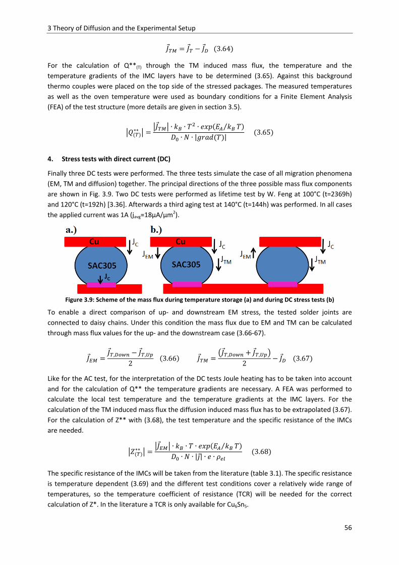
3 Theory of Diffusion and the Experimental Setup
56
l- l l3.64 For the calculation of Q**(T) through the TM induced mass flux, the temperature and the
temperature gradients of the IMC layers have to be determined (3.65). Against this background
thermo couples were placed on the top side of the stressed packages. The measured temperatures
as well as the oven temperature were used as boundary conditions for a Finite Element Analysis
(FEA) of the test structure (more details are given in section 3.5).
∗∗ l- ∙ KL ∙ M ∙ <J KL⁄ M 6 ∙ ∙ |"Rt$M | 3.65
4. Stress tests with direct current (DC)
Finally three DC tests were performed. The three tests simulate the case of all migration phenomena
(EM, TM and diffusion) together. The principal directions of the three possible mass flux components
are shown in Fig. 3.9. Two DC tests were performed as lifetime test by W. Feng at 100°C (t=2369h)
and 120°C (t=192h) [3.36]. Afterwards a third aging test at 140°C (t=144h) was performed. In all cases
the applied current was 1A (javg=18µA/µm2).
Figure 3.9: Scheme of the mass flux during temperature storage (a) and during DC stress tests (b)
To enable a direct comparison of up- and downstream EM stress, the tested solder joints are
connected to daisy chains. Under this condition the mass flux due to EM and TM can be calculated
through mass flux values for the up- and the downstream case (3.66-67).
lU- l,~Éh l,ÊV2 3.66 l- 3l,~Éh & l,ÊV52 l3.67 Like for the AC test, for the interpretation of the DC tests Joule heating has to be taken into account
and for the calculation of Q** the temperature gradients are necessary. A FEA was performed to
calculate the local test temperature and the temperature gradients at the IMC layers. For the
calculation of the TM induced mass flux the diffusion induced mass flux has to be extrapolated (3.67).
For the calculation of Z** with (3.68), the test temperature and the specific resistance of the IMCs
are needed.
o ∗∗ lU- ∙ KL ∙ M ∙ <J KL⁄ M 6 ∙ ∙ |f| ∙ ∙ Gq 3.68
The specific resistance of the IMCs will be taken from the literature (table 3.1). The specific resistance
is temperature dependent (3.69) and the different test conditions cover a relatively wide range of
temperatures, so the temperature coefficient of resistance (TCR) will be needed for the correct
calculation of Z*. In the literature a TCR is only available for Cu6Sn5.

3 Theory of Diffusion and the Experimental Setup
57
Gq ∙ 1 & M!s ∙ M M 3.69 Cu6Sn5 Cu3Sn
ρel [Ωµm] 0.175 [3.37] 89.3x10⁻³ [3.37] TCR [1/K] 3.5x10⁻³ [3.38] n.a.
Table 3.1: Specific resistance and TCR of the IMC layers.
3.3.2 Experimental Setup For all tests Amkor® Package-on-Package (PoP) structures with a size of 12x12mm were used. The
PoP structures include two packages being connected with two different Ball Grid Arrays (BGAs). An
illustration of the PoP structure is given in Fig 3.10.
Figure 3.10: An Illustration (a) [3.39] and a X-Ray picture (b) [3.36] of the PoP test structure
The BGA of the top package is formed out of 128 SnAg3.0Cu0.5 (SAC305) solder joints. Their contact
pads on the die and the board side are covered with an Electroless Nickel Gold (ENIG) layer as
diffusion barrier for Cu atoms coming from the metal lines (“closed system”).
The BGA of the bottom package includes 305 SnAg3.0Cu0.5 solder joints. Their die side contact surfaces
are directly connected to the Cu pads, while the board side contact pads are covered with NiP (Fig.
3.11). Due to the missing diffusion barrier at the die side Cu atoms can flow from the die side contact
pads into the bottom bumps (“open system”).
Figure 3.11: Illustration of a closed system with Ni diffusion barriers (left) and an open system without Ni
barrier at the die side (right)
The long term temperature storage tests were performed with single packages. For the DC-EM and
the AC-TM tests FR-4 boards with 24 packages per board were used (Fig. 3.12, left). For the thermal

3 Theory of Diffusion and the Experimental Setup
58
aging tests as well as for the DC-EM and AC-TM tests the single packages and the test boards were
placed in ovens. The test boards were designed to compare EM reliability tests with temperature
storage tests [3.36], so the contact pins in the middle of the cards allow the application of a current
on single packages. During the AC-TM and the DC-EM tests one half of the packages were current
stressed while the other packages were temperature stressed only. Afterwards the influence of a TM
or EM induced mass flux on the IMC formation was clarified by comparing the AC-TM and the DC-EM
test results with the IMCs in the temperature stressed packages.
As shown in Fig 3.12 the solder joints are connected to daisy chains. The daisy chains are divided into
sub chains: "a1" to "a4", "b1" to "b4", "c1" to "c4" and "d1" to "d4" for the bottom packages, and "A"
and "B" for the top packages. The daisy chains are accessible over contact pads on the FR-4 board
which enables resistance measurements on single sub chains.
During the DC-EM tests a constant current source (Sodilec 60V 5A) guaranteed a constant driving
force, even if the resistance of the daisy chains increases due to material degradation. That means
the performed EM tests were "constant current tests". For the AC tests normal line voltage
(230V/50Hz) was transformed (24V/50Hz) and the applied current was limited with a manual
potentiometer. For the documentation of the tests a multimeter (Keithley 2000) and a LabView®
program were used.
Figure 3.12: Test card used for electromigration tests (left), order of the daisy chains in the top and bottom
packages and position of the sub chains (right) [3.36]
3.3.3 Sample Preparation and Analysis After the stress tests the PoP structures were prepared for the following analysis steps. The short
term temperature stressed and the current stressed packages were sawn out of the FR-4 test boards
(Fig. 3.13 right). As shown in Fig 3.13 (middle) the single packages from the long term temperature
storage tests and the packages being separated from the FR-4 boards were embedded into an epoxy
resin (Struers EpoFix: see data sheet for more details). To verify the starting point of the IMC growth
during the aging tests, non-stressed packages were embedded into resin too. Afterwards the
samples were polished with sandpaper (SiC) until the cross section surface reached the BGAs. For
the SiC foils grit sizes (ISO 6344) between 220 (average particle diameter: davg= 68µm) and 2000 (davg=
10.3µm) were chosen. Afterwards the cross section surfaces were diamond polished (davg= 3µm-
0.25µm) until the IMC layers in the solder joints were clearly visible.

3 Theory of Diffusion and the Experimental Setup
59
Figure 3.13: Different steps of the sample preparation: single package (left), embedded package prepared for
optical microscopy (middle), and for SEM+EDS (right)
The identification of the IMC layers as well as most of the geometrical measurements were made
through light microscopy. For the geometrical measurements and the documentation of the results a
microscope camera and the Nikon Imaging System were used. The maximum magnification of the
light microscope was 1000x and its maximum resolution was in the range of 250nm.
With respect to the limited resolution of the light microscope a scanning electron microscope (SEM)
was used (JEOL: JSM-6100, Fig. 3.14) for the investigation of relatively thin IMC layers (h<1µm). Due
to the electrically nonconductive resin, the probes had to be coated with a silver paste and the areas
of interest had to be covered with a 10-15nm thick carbon layer (Fig 3.13, right). For the geometrical
measurements the secondary electron (SE-SEM) detector and for the identification of different IMC
layers the back scattered electron (BSE-SEM) detector were used. In addition to the electron
detection the spectrum of the X-Ray radiation was analyzed through EDS (Oxford Instruments: INCA
x-act). Taking into account the presence of the carbon layer the EDS enables the determination of
IMC composition with a precision of +/-1 mass percent.
Figure 3.14: Scanning Electron Microscope (left) and X-Ray spectrometer (right) at the IMS of the Université
Bordeaux I
The measured IMC thickness will show relatively strong variations being caused by different
influences on the final test results:
• Variations in the microstructure of the SnAgCu solder and the presence of grain boundaries as
diffusion paths. Especially during the DC and AC stress tests annealing in different degrees of
intensity can lead to a more or less intensive coarsening of the grain structure [3.40].
• Variations in the Cu content of the SnAgCu solder, being mainly relevant for the closed system
of the top bumps.
• Different starting points for the IMC growth due to variations of the process temperature and
the process time during the reflow.
• Temperature variations in the oven, in the packages and on the test boards.

3 Theory of Diffusion and the Experimental Setup
60
As consequence of possible variations of the IMC thickness, for every data point at least 24 solder
joints will be investigated. This finally leads to several hundred light microscopy pictures and dozens
of SE-SEM and BSE-SEM investigations. Furthermore several hundred EDS measurements were made
to verify the composition of the relevant materials. For the analysis of the data statistical methods
were used; mainly performed with Origin 8.5.
3.4 Migration Induced Intermetallic Compound Growth For the determination of the migration related material parameters the mass flux values have to be
extracted from the experimental results. In this section equation for the calculation of migration
induced mass flux from the IMC growth speed will be derived. In the following this equation will be
transformed for the use on Cu-Sn and Cu-Ni-Sn IMCs.
3.4.1 General Model of Migration Induced IMC Formation The first step of the derivation is the calculation of the atomic density (N) of every element in the
IMC. This was done through the mass fraction “m” being determined with EDS before.
With the mass fractions of the single elements in the IMCs (e.g. Cu or Sn) and their mass density (ρ) it
is possible to estimate the mass density of the IMCs through (3.70). The equation ignores lattice
stacking effects.
,-. Ëgg Ì 3.70)g
i = components, e.g. for (CuNi)6Sn5: i=4 for Cu, Sn, Ni and Au
With the mass density and the IMC volume (V) the mass of the IMC layer (M) can be calculated (3.71)
and with the mass fraction the partial mass of the single components (3.72).
= = ,-. ∙ *,-. (3.71) =g = = ∙ g (3.72)
With the atomic mass (M) of a component and its partial mass, the total number of its atoms in the
IMC layer (n) can be calculated (3.73). The atomic number divided by the IMC volume finally leads to
atomic density of the component (3.74).
g = = ∙ g=g (3.73) g = g*,-. = = ∙ g=g ∙ *,-. = ,-. ∙ g=g (3.74)
The change of the atom number over time defines the effective mass flux into the IMC layer (3.75).
At the contact pads the shape of the solder joints is nearly cylindrical and as a consequence only the
vertical IMC growth will be taken into account. For the calculation of the mass flux, the IMC thickness
before (h0) and after the aging tests (h) has to be known. The starting point for the IMC growth is the
IMC thickness after the reflow process. Based on these assumptions (3.76) describes the mass flux of
a chosen element (i). For the use of (3.76), the test time (ttest) is needed and the mass fraction and
the material density of the IMC have to be known as functions of time.
lg() = 1) Î3Ï(H,¿,À,)5$*Ð = 1)=g ∙ Î3Ï(H,¿,À,),-.(H,¿,À,)5$*Ð (3.75)

3 Theory of Diffusion and the Experimental Setup
61
lHg 1=g ∙ Ñ 3ÏH, ,-.H, 5$Ð/
/©3.76
For the following steps the mass flux will be assumed to be constant over the test time (ttest). Before
an accurate mass flux calculation is possible this assumption has to be checked for the chosen test
times with long term temperature tests (see section 3.3.1). In case of a nearly constant IMC growth
speed the average mass flux is given by (3.77).
∆g) lg,JÒÓ ∙ GD 1=g ∙ Ô 3ÏH, ,-.H, 5$Ð
ÕÖ×Õ/
/©$3.77
For the following step it will be assumed that:
1. an average atomic density of every component can be used for the resulting IMC. This means,
that next to the source for the inflow of the relevant component into the investigated IMC layer,
the concentration of this component has to be as high as possible (Fig. 3.15). At the opposite
interface the minimum concentration of the element in the investigated IMC layer should be
found.
2. If a critical concentration of this element is reached, the formation of a new IMC begins. This
process needs much less time than the aging tests themselves. The second point is not critical
because the Debye frequency enables hundreds of billions of reactions per second while the
aging tests go over dozens of hours.
Figure 3.15: Simplified configuration for the migration induced growth of three different IMCs with a
shrinking atomic density (N) of the element “i” e.g. i=Cu
As a consequence of these assumptions the integral over time can be replaced by a sum of the
atomic densities of the chosen element in the relevant layers (3.78). The value of Z is the number of
the relevant layers minus one. For example: if Cu flows from the contact pads (first layer) into Cu3Sn
(second layer) and the growing Cu3Sn layer replaces Cu6Sn5 (third layer) Z=2.
lg,JÒÓ 1=g ∙ GD ∙ Ñ g,hH ,-.,hH $
/ØÙÚ/Ø
¹
h 4¹ 44¹ 43.78
Z+1 = Number of the relevant layers.

3 Theory of Diffusion and the Experimental Setup
62
Taking into account that the concentration gradients in the IMCs are small compared to the atomic
density (grad(Ni)dn<<N) [3.2] the atomic density in the IMC will be defined to be isotropic. Under this
condition the mass flux in the IMC can be calculated with an additive formula (3.79a-b):
lg,JÒÓ = 1=g ∙ GD ∙ g,h,-.,h ∙ (ℎh − ℎh)¹
h (3.79t)
lg,JÒÓ = 1GD ∙ g,h ∙ (ℎh − ℎh)¹
h (3.79')
During the previous steps the geometrical values “hn” were related to specific IMC layers, this was
done for more clarity but it is not a must. Hence if a relevant concentration gradient is present in the
IMC layers, they can be divided into several parts without changing (3.79) in principle. Due to this
fact Z is related to “layers” and not to materials. Hence the use of (3.79) is possible for anisotropic
IMCs, but the value “Z” and the resulting computing time will be higher than for isotropic IMCs.
As described by the Deal-Grove model the IMC formation speed slows done over time. Hence for a
long testing time the assumption of a constant mass flux over time is not sufficient. Nevertheless the
accuracy of the calculation can be improved by a linear approximation of the resulting square root
curve. In this case the test time has to be divided into intermediate steps (tn) and the resulting mass
flux is described by a double sum (3.80). The time steps used have to be chosen through long term
temperature storage tests.
lg,JÒÓ = 1=g ∙ Û 1(Ü − Ü) ∙ g,h,-.,h ∙ (ℎh − ℎh)¹
hÝ
Þ
Ü (3.80)
GD = Þ = 0 ℎ = ℎ(ß)
3.4.2 Adaptation of the IMC Growth Model for the Cu-Ni-Sn and Cu-Sn Formation For this study Amkor® Package-on-Package (PoP) structures were used. The PoP structures are based
on two different BGAs. For the top package the contact pads are covered with a NiAu layer. As
consequence no Cu migration from the Cu Pads into the solder joints was possible: “closed system”
(Fig. 3.11).
The solder joints of the bottom package were directly connected to the Cu pads on the die side,
while the board side contact pads are covered with NiP. Hence Cu can flow from the die side contacts
into the solder joints: “open system”.
Hence the investigation of the migration induced IMC formation has to be done for two principal
cases: the “open system” with a direct contact between Cu and SnAg3.0Cu0.5 and the “closed system”
with two diffusion barriers between Cu and SnAg3.0Cu0.5. For both cases different adaptations of the
mass flux equation (3.78) will be necessary.

3 Theory of Diffusion and the Experimental Setup
63
3.4.2.1 Open System In an open system the formation of Cu3Sn and Cu6Sn5 can be expected. Both IMCs grow in two
directions: in case of Cu3Sn the IMC growth into two directions appears because the inclusion of Sn at
the Cu pads transforms Cu into the Cu3Sn, while the inflow of Cu at the Cu3Sn/Cu6Sn5 interfaces leads
to Cu3Sn formation too (Fig 3.16). During the Cu6Sn5 growth the inclusion of Sn transforms Cu3Sn to
Cu6Sn5 and at the Cu6Sn5/SnAgCu interface additional Cu6Sn5 is formed by the inflow of Cu into
SnAgCu.
Figure 3.16: Principal Cu migration during the IMC growth on an open system
The formation of IMCs in both directions leads to the measurable increase of the IMC layer thickness
during the aging tests (3.81). The mobility of Cu and Sn in Cu3Sn and Cu6Sn5 is different and the
interfaces between the IMCs act as vacancy sinks or sources [3.10]. As a consequence the mass fluxes
in Cu3Sn and Cu6Sn5 have to be calculated independent from each other. Furthermore the IMC
growth mechanism is simplified by the assumption that the IMC composition stays the same during
the aging tests. (3.82).
4 4 4Ü & 4q 3.81 lg,JÒÓ lgÜ lgq3.82 For the calculation of the mass flux values at both interfaces (3.79b) can be used with Z=0:
lgÜ 4ÜGD ∙ 3g,, g,,,53.83t lgq 4qGD ∙ 3g,,, g,,,,53.83' I,II,III= the meaning of these indices is given in table 3.2
Phase II=Cu3Sn II=Cu6Sn5
Indices I=Cu III=Cu6Sn5 I=Cu3Sn III=SnAgCu Table 3.2: Indices for the Eqs. 3.82-3.85 with NCu,SnAgCu=0 and NSn,Cu=0.
The values dr and dl cannot be measured separately, but they become available by inserting (3.83a-b)
into (3.82) and the resulting (3.84) into (3.81). The final results are Eqs. (3.85a-b).
4Ü 3g,,, g,,,,53g,, g,,,5 ∙ 4q 3.84
4Ü 4 4 ∙ 3g,,, g,,,,53g,, g,,,,5 3.85t 4q 4 4 ∙ 3g,, g,,,5
3g,, g,,,,53.85'

3 Theory of Diffusion and the Experimental Setup
64
Using (3.79b) with Z=1 and inserting (3.85a-b) into (3.79b) leads to mass flux of Cu and Sn in Cu3Sn
and Cu6Sn5 (3.86a-b). It was taken into account that the growth of the IMC layers into the solder joint
(Δh=hl) is related to the inflow of Cu from the contact pads, while the IMC growth into the opposite
direction (Δh=hr) is related to the inclusion of Sn.
l.,,, = lq = (ℎ − ℎ)GD ∙ 3.,, − .,,,53.,, − .,,,,5 ∙ 3.,,, − .,,,,5 (3.86t)
lh,,, = lÜ = (ℎ − ℎ)GD ∙ 3h,,, − h,,,,53h,, − h,,,,5 ∙ 3h,,, − h,,,,5 (3.86')
3.4.2.2 Closed System The pending question about the closed system is: if Ni3Sn4 is formed in SnAgCu during the stress test
or not and if it is formed, what are the conditions? Meanwhile the formation of (CuNi)6Sn5 is certain
for all test conditions. For the analysis of the test results two principal equations will be used. The
first describes the migration of Cu, Au and Ni when (CuNi)6Sn5 is formed. The second describes the
motion of Ni if (CuNi)6Sn5 and Ni3Sn4 are formed. For the second case an additional interpretation of
the Cu or Au flux is not necessary, because the related accumulation process (section 3.2) appears at
the SnAgCu to (CuNi)6Sn5 interface and is not affected by the Ni3Sn4 formation.
For the derivation of (3.87), describing the Ni flux from the Pad into (CuNi)6Sn5, the same principals as
for the description of the Cu flux from the contact pads into an open system can be used (3.85a).
With NNi,SAC=0 the resulting equation for the mass flux is (3.87):
lmg,.mgh = lq = (ℎ − ℎ)GD ∙ @1 − mg,.mghmg,mg C ∙ 3mg,.mgh5 (3.87)
The accumulation of Cu and Au in (CuNi)6Sn5 does not go along with an observable dissolution of the
Ni pad. Hence the mass flux equations for Cu and Au are given through (3.78b) with Z=1 (3.88):
lg,JÒÓ = (ℎ − ℎ)GD ∙ 3g,.mgh − g,J.5 (3.88)
i = Cu or Au
If Ni3Sn4 and (CuNi)6Sn5 are formed, the equation for the calculation of the Ni flux has to cover both
IMCs. In this case the growth of (CuNi)6Sn5 does not lead to a consumption of the Ni pad, but the
formation of Ni3Sn4 does. So the final equation is a sum of (3.87) and (3.88) with NNi,SAC=0 (3.89a-b):
lmg = lmg,mgh + lmg,.mgh (3.89t)
lmg = ℎmghGD ∙ @1 − mg,mghmg,mg C ∙ 3mg,mgh − mg,.mgh5 + (ℎ − ℎ).mghGD ∙ 3mg,.mgh5 (3.89') The Au concentration in Ni3Sn4 is very low. Hence (3.88) is also sufficient for the analysis of the Au
mass flux if the formation of Ni3Sn4 appears. For the mass flux of Cu the same approach as for Ni can
be used, but the consumption of the Ni pad is not relevant (3.90a-b):
l. = l.,mgh + l.,.mgh (3.90t)

3 Theory of Diffusion and the Experimental Setup
65
l. 4mghGD ∙ 3.,mgh5 & 4 4 .mghGD ∙ 3.,.mgh .,J.53.90'
3.5 Preparation of the Finite Element Analysis A Finite Element Analysis (FEA) of the test structure was performed with ANSYS® to get the exact test
temperatures under consideration of Joule heating. Furthermore the temperature gradients in the
IMC layers were needed. For the creation of the model the geometrical data of the solder joints and
the surrounding package were measured through light microscopy and implemented by the
parameter design language of ANSYS® (APDL). Afterwards the relevant material parameters for every
component were defined by literature values.
After the analysis of aging tests the resulting material parameters of the migration induced mass flux
in the IMC layers will be used for a dynamic simulation of the IMC growth. For this task a user
routine was developed.
3.5.1 Model Geometry For the FEA, two top bumps, two bottom bumps, a part of the package and a part the FR-4 test board
were modeled. A detailed illustration of the model is given by Fig. 3.17. The top and the bottom
solder joints are connected with Cu metal layers (M1-M4). For all geometrical parameters being
relevant for current crowding, like the contact pad diameters or the metal layer height, the mean
values of several dozen measurements and their standards deviations (sd) are available [3.42].
Figure 3.17: Finite Element model of the PoP (left) structure, the top (middle) and the bottom (right) bumps
M.C.: Mold Compound, S.R.M.: Solder Resist Mask
For the determination of the bump height or the metal layer thickness (table 3.3) the light
microscopy data could be used without an additional interpretation, but in case of the contact pad
diameters and the bump diameters further investigations were necessary.
M1 M2 M3 M4
29 +/- 3µm 17.8 +/- 2.5µm 13.3 +/- 2.1µm 14 +/- 1.4µm Table 3.3: Thickness of the four relevant metallization layers.
The contact pad diameters were determined through light microcopy measurements of the top side
of non-soldered bottom packages (Fig. 3.18, left). In the data sheets the principle solder bump
diameters can be found (Top: 450µm, Bottom: 300µm [3.41 p.5]), but unlike the contact pad

3 Theory of Diffusion and the Experimental Setup
66
diameters the final bump diameters depend on the pressure used during the reflow process and the
viscosity of the solder. Hence the bump diameter values in the data sheets have to be verified for the
actual test structures. A direct measurement of the diameter is impossible because the measured
diameter values on a two dimensional cross section surface do not have to be the real diameters of
the three dimensional solder bumps (Fig. 3.18, right). Nevertheless, knowing the contact diameter, it
is possible to reconstruct the bump diameters with (3.91). Furthermore the profile of the cross
section surface can be visualized by calculating its distance to the center of the bumps (3.92).
6L,YEH á6L & 6.,YEH 6.3.91 DB,max= real bump diameter; DB= measured bump diameter at the cross section surface;
DC,max= real contact pad diameter; DC= measured contact pad diameter at the cross section surface
12 ∙ @á6L,YEH 6LC 1
2 ∙ @á6.,YEH 6.C3.92 SD= Distance between the cross section surface and the center of the bump.
Figure 3.18: Contact pad on the top of a non-soldered bottom package (left), and the principal relation
between the real bump diameter and the measured diameter at the cross section surface (right)
In Fig 3.19 the measured diameters on the cross section surface of five different samples are shown.
Furthermore the related surface profiles as results of (3.92) are given. The combination of both
pictures shows the relation between the measured diameters and the cross section surface profile:
• the measured diameters strongly depend on the distance between the bump center and the cross
section surface. So the measured diameter for the samples “120°C”, “120°C/1A” and “100°C/1A”
clearly differ from the measured diameters of the samples “100°C” and “ref”.
• a warpage of the cross section surface as result of over polishing increases the standard deviation
of the diameter (sample "120°C").
• a decline of the cross section surface (sample “120°C/1A”), which appears as consequence of a
torque being created by the friction force between the rotating grinding disc and the polished
sample, leads to a distorted distribution of the bump diameter values.

3 Theory of Diffusion and the Experimental Setup
67
Figure 3.19: Box plots of the measured top bump diameters separated by the stress test conditions (left) and
the surface profile of the related samples (right) [3.42]
In addition (3.90) can be used to calculate the correct bump diameters out of the measured diameter
values. The visualization of the measured diameters (Fig. 3.20) before and after correction with
(3.90) shows better correlation of the corrected values to the expected normal distribution of the
bump diameters.
Figure 3.20: Distribution of the top bump diameters before (a) and after the adjustment (b) [3.42]
An alternative way to measure the bump diameters after the reflow process are X-Ray pictures of the
PoP structures. Nevertheless the accuracy of the X-ray measurements was limited and their relative
standard deviation was 10%, so the resulting diameters are approximate values only. Finally the
bump diameter values from four different sources can be compared (table 3.4) and the influence of
the reflow process and the package warpage on the bump diameters can be described. In general the
deformation of the solder joints appears due to the pressure being applied during the soldering and
due to the package warpage. Both effects increased the diameter bump diameters compared to data
sheet values. For the smaller bottom bumps the effect is more relevant, because the process
influences are combined with smaller bump diameters. The variation of the bump geometry has an
influence on the current crowding effect and the expected lifetime of the solder joints under EM
stress. More details about the relation between lifetime and geometry variations are given in [3.42]
Source: Data sheet Microscope X-ray Real
Top 450µm 459 +/- 21µm 470µm 481 +/- 8µm
Bottom 300µm 348 +/- 36µm 376µm 363 +/- 11µm Table 3.4: Diameter of the top and bottom bumps.

3 Theory of Diffusion and the Experimental Setup
68
3.5.2 Material Parameters and the Boundary Conditions For the thermal electrical simulation the different packaging materials have to be defined by their
specific resistance and their thermal conductivity. This was done for a temperature range from 200K
(-73.16°C) to 600K (326.84°C).
3.5.2.1 Specific resistance (ρel) All electrical conductive materials in the package are metals. Their temperature dependent specific
resistance was defined by a linear model (3.69) with a TCR (table 3.5). The TCR of the IMCs was only
available for Cu6Sn5. For (CuNi)6Sn5 the same value as for Cu6Sn5 was used. The TCR, of Cu3Sn and
Ni3Sn4 have to be extracted from the experimental results.
Material Cu Ni SnAgCu Cu6Sn5/(CuNi)6Sn5
TCR [1/K] 3.85x10⁻³ [3.43] 6.44x10⁻³ [3.44] 2.8x10⁻³ [3.43] 3.5x10⁻³ [3.38] Table 3.5: TCR of the metals and IMCs in the PoP structure.
The specific resistances of all other materials were assumed to be temperature-independent:
Material/Temperature 200K 300K 400K 500K 600K
Copper [3.43] 10.6x10⁻³ 17.4x10⁻³ 23.1 x10⁻³ 30.7x10⁻³ 37.3x10⁻³
Nickel [3.44] 23.7x10⁻³ 66.9x10⁻³ 0.11 0.153 0.196
NiP [3.45-46] 0.669 0.7 0.732 0.763 0.795
Cu6Sn5/(CuNi)6Sn5 [3.37] 93.6x10⁻³ 0.175 0.254 0.333 0.411
S.R.M. [3.47] 0.2x10¹⁸
FR-4 [3.48] 0.5x10¹⁵
SnAgCu [3.43] 96x10-3 0.132 0.169 0.207 0.244
Resin [3.49] 1x10¹⁸
M.C.[3.50] 10x1015
Cu3Sn* [3.37] 61.9x10⁻³ 89.3x10⁻³ 0.117 0.144 0.172
Ni3Sn4 [3.37] 87.2x10⁻³ 0.285 0.483 0.681 0.878 Table 3.6: Specific resistances of the used materials [Ωµm].
3.5.2.2 Thermal conductivity (κ) In metals the thermal transport is mainly done by the electron gas and as a consequence the thermal
conductivity is proportional to the electrical conductivity. The relation between the thermal and the
electrical conductivity is described by the Wiedemann Franz law (3.93):
¸ b ∙ KL3 ∙ ∙ M ∙ 1 + M!s ∙ (M − M) (3.93)
For the nonmetals temperature independent values were implemented. Due to the fiberglass
content the thermal conductivity of the FR-4 board is anisotropic. For (CuNi)6Sn5 the same value as
for Cu6Sn5 were used.

3 Theory of Diffusion and the Experimental Setup
69
Material/Temperature 200K 300K 400K 500K 600K
Copper [3.43] 460x10-6 421x10-6 405x10-6 398x10-6 393x10-6
Nickel [3.44] 0.206x10⁻³ 0.11x10⁻³ 88.8x10⁻⁶ 79.8x10⁻⁶ 73.8x10⁻⁶
Cu6Sn5/(CuNi)6Sn5 [3.37] 62x10-6 33.1x10⁻⁶ 23.5x10⁻⁶ 17.9x10⁻⁶ 13.5x10⁻⁶
S.R.M. [3.47] 0.21x10⁻⁶
FR-4 [3.48]
x 1.05x10-6
y 0.34x10⁻⁶
z 1.05x10⁻⁶
SnAgCu [3.43] 50.83x10⁻⁶ 55.52x10⁻⁶ 57.82x10⁻⁶ 59x10-6 60.07x10⁻⁶
NiP [3.45-46] 8.83x10⁻⁶ 8.0x10⁻⁶ 7.66x10⁻⁶ 7.34x10⁻⁶ 7.05x10⁻⁶
Resin [3.49] 0.2x10⁻⁶
M.C.[3.50] 0.167x10⁻⁶
Cu3Sn [3.37] 0.1x10⁻³ 70.4x10⁻⁶ 53.9x10⁻⁶ 43.6x10⁻⁶ 36.6x10⁻⁶
Ni3Sn4 [3.37] 63.1x10⁻⁶ 19.6x10⁻⁶ 11.6x10⁻⁶ 8.21x10⁻⁶ 6.36x10⁻⁶ Table 3.7: Thermal conductivity of the used materials [W/(µmK)].
3.5.2.3 Implementation of the Boundary Conditions The main task of the simulation is the calculation of the test temperature at the IMC layers and the
determination of temperature distribution under consideration of Joule heating. Against this
background thermocouples were placed on the PoP structures and the package temperature was
recorded during the AC and the DC stress tests. Later the measured temperatures were used to
define the thermal boundary conditions for the FEA.
At upper ends of the metal layers the input currents and the grounds were placed (Fig. 3.21, left).
The arrangement of the metal lines represents the bump chains in the real packages and enables the
simulation of the up- and the downstream case. To ensure a correct calculation of the local
temperature gradients at the contact surfaces, the model also includes IMC layers (Fig. 3.21, middle,
right).
Figure 3.21: FE Model of the bump chain (left) and a detailed view on the implemented IMC layers (right)
On the free standing surfaces of the Finite Element (FE) model a temperature dependent heat
transmission coefficient (HTC) has to be defined. The HTC represents the heat loss due to convection
and radiation. A model of four solder joints represents only a small part of the package or the whole
test board surface. Hence a variable HTC was set up at the top and the bottom surface of the FE
model, while the oven temperature was set as ambient temperature. Afterwards an optimization
algorithm of ANSYS® was used to determine an HTC which represents the heat flux over the total
package or test board surface. The target values of the optimization algorithm are the recorded
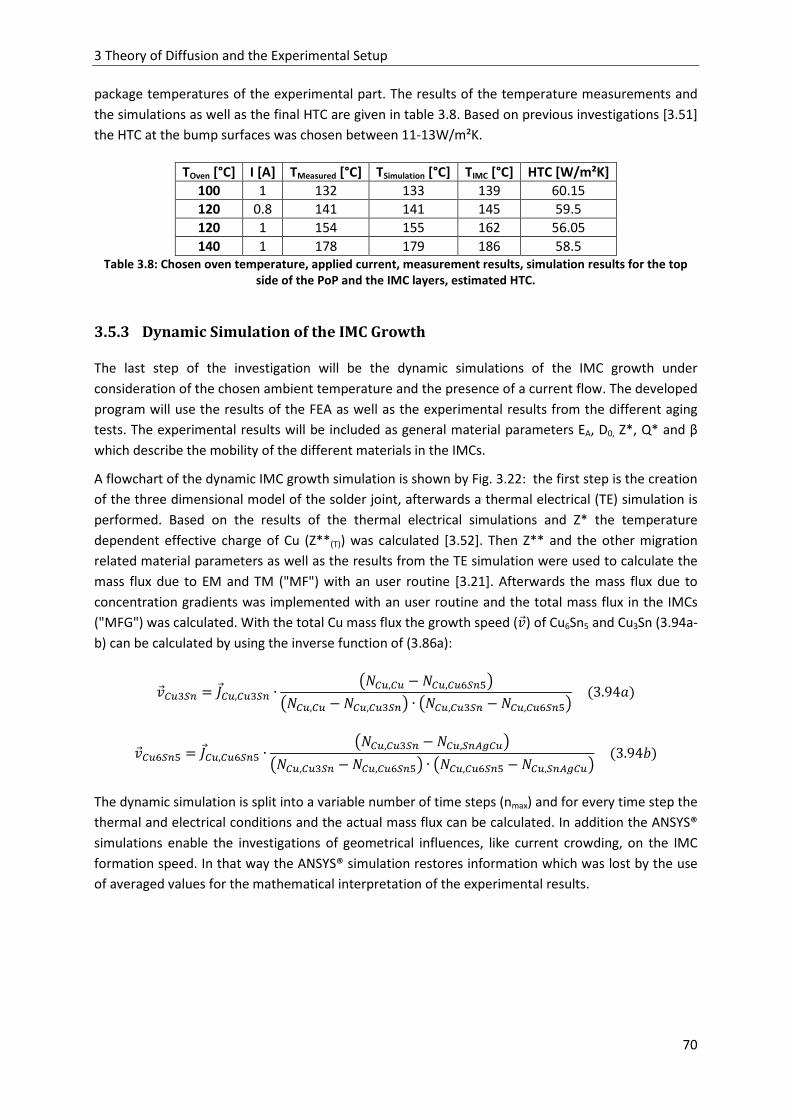
3 Theory of Diffusion and the Experimental Setup
70
package temperatures of the experimental part. The results of the temperature measurements and
the simulations as well as the final HTC are given in table 3.8. Based on previous investigations [3.51]
the HTC at the bump surfaces was chosen between 11-13W/m²K.
TOven [°C] I [A] TMeasured [°C] TSimulation [°C] TIMC [°C] HTC [W/m²K]
100 1 132 133 139 60.15
120 0.8 141 141 145 59.5
120 1 154 155 162 56.05
140 1 178 179 186 58.5 Table 3.8: Chosen oven temperature, applied current, measurement results, simulation results for the top
side of the PoP and the IMC layers, estimated HTC.
3.5.3 Dynamic Simulation of the IMC Growth The last step of the investigation will be the dynamic simulations of the IMC growth under
consideration of the chosen ambient temperature and the presence of a current flow. The developed
program will use the results of the FEA as well as the experimental results from the different aging
tests. The experimental results will be included as general material parameters EA, D0, Z*, Q* and β
which describe the mobility of the different materials in the IMCs.
A flowchart of the dynamic IMC growth simulation is shown by Fig. 3.22: the first step is the creation
of the three dimensional model of the solder joint, afterwards a thermal electrical (TE) simulation is
performed. Based on the results of the thermal electrical simulations and Z* the temperature
dependent effective charge of Cu (Z**(T)) was calculated [3.52]. Then Z** and the other migration
related material parameters as well as the results from the TE simulation were used to calculate the
mass flux due to EM and TM ("MF") with an user routine [3.21]. Afterwards the mass flux due to
concentration gradients was implemented with an user routine and the total mass flux in the IMCs
("MFG") was calculated. With the total Cu mass flux the growth speed (e) of Cu6Sn5 and Cu3Sn (3.94a-
b) can be calculated by using the inverse function of (3.86a):
e.2h l.,.2h ∙ 3.,. − .,.h53.,. − .,.2h5 ∙ 3.,.2h − .,.h5 (3.94t)
e.h = l.,.h ∙ 3.,.2h − .,hJÓ.53.,.2h − .,.h5 ∙ 3.,.h − .,hJÓ.5 (3.94')
The dynamic simulation is split into a variable number of time steps (nmax) and for every time step the
thermal and electrical conditions and the actual mass flux can be calculated. In addition the ANSYS®
simulations enable the investigations of geometrical influences, like current crowding, on the IMC
formation speed. In that way the ANSYS® simulation restores information which was lost by the use
of averaged values for the mathematical interpretation of the experimental results.

3 Theory of Diffusion and the Experimental Setup
71
Figure 3.22: Flowchart for the dynamic simulation of the IMC growth
3.6 Conclusion For the IMC formation in solder joints different migration phenomena are relevant. Based on
different aging tests these phenomena have to be described separately and a general model of the
IMC growth has to be developed.
During the aging tests two transport mechanisms are relevant: the interstitial diffusion of noble
metals in the tin solder and the vacancy mechanism for the material transport in the IMCs. Based on
the solution of the random walk problem and the resulting Nernst-Einstein equation the physical
interpretation of the diffusion related material parameters like the activation energy (EA), the
diffusion coefficient (D) and the diffusion constant (D0) is possible. Nevertheless the complex crystal
structure of the IMCs and the presence of grain boundaries do not allow a direct calculation of these
parameters from known material values. Nevertheless the Nernst-Einstein equation can be used to
describe migration phenomena due to external driving forces, like an applied current (EM),
temperature gradients (TM) or local differences in the solubility of an element in the investigated
binary compounds. Furthermore the definition of independent material parameters for the different
migration phenomena is possible: like the effective charge of the moving ion (Z*) in case of EM, the
heat of transport (Q*) for TM, as well as an driving force “β” for the migration due to differences in
the solubility. As for EA and D0 the complex crystal structure of the IMCs and the high defect density
due to grain boundaries disables the direct calculation of the migration related material parameters.
Hence an experimental determination is needed. Overall four different experiments have to be
performed to characterize the IMC formation in the solder joints (table 3.9).

3 Theory of Diffusion and the Experimental Setup
72
Test Migration mechanism IMC features Parameter extracted
Temperature storage
long term
Diffusion
Accumulation
Time dependency of
the IMC formation
speed
Time limit for a
constant IMC
formation speed.
Temperature storage
short term
Diffusion
Accumulation
Temperature
dependency of the
IMC formation speed
Activation Energy (EA)
Diffusion Constant (D0)
Driving force (β)
Temperature storage
+ AC current load
Diffusion + Accumulation
+ Thermomigration
Increased/Decreased
IMC formation speed
at the die/board side
TM downstream
Heat of transport (Q*)
Temperature storage + DC current load
(use case)
Diffusion + Accumulation + Thermomigration
+ Electromigration
Downstream case
Increased/Decreased
IMC formation speed at the die/board side
Upstream case
Decreased/Increased
IMC formation speed
at the die/board side
Effective charge (Z*) Heat of transport (Q*)
Heat of solution (H)
Table 3.9.Summary of the test procedures and the extracted material parameters.
For the experiments single packages and test boards with 24 packages will be used. After the aging
tests cross sections of the packages will be made. Afterwards the dimensions of the IMCs will be
measured with light microscopy and SEM and their material composition has to be determined with
EDS.
The main result of the aging tests should be an increased IMC layer thickness compared to the
starting point. The starting point was defined by the IMC layer thickness after the reflow soldering.
Against this background a mathematical model for the calculation of the average mass flux in the
IMCs was developed from their growth speed during the aging test.
The applied current, which is needed for the EM and TM tests, leads to Joule heating. Hence a FEA
will be needed to get the exact test temperature at the IMC layers and the temperature gradients.
The temperature gradients were used for the analysis of the TM induced mass flux and for the
determination of Q*.
When all migration related material parameters are available, the FEM will also be used to perform a
dynamic simulation of the IMC growth. The simulations will be done under the consideration of the
ambient temperature, the applied current and the three dimensional shape of the investigated
solder joints.

4 Migration Induced IMC Growth in SnAgCu Solder Bumps
73
4 Migration Induced IMC Growth in SnAgCu Solder Bumps

4 Migration Induced IMC Growth in SnAgCu Solder Bumps
74
In this chapter the results of the temperature storage (TS) tests, the TM-AC tests and the EM-DC tests
will be given for the bottom bumps (“open system”) and the top bumps (“closed system”).
By comparing the IMC formation speed at different test conditions the mass flux values due
diffusion, material accumulation, TM and EM will be extracted. Based on these values the
experimental material parameters will be calculated. If necessary a further interpretation of these
values will be given. In this case especially the difference between the crystal structure of fcc metals
and the IMCs will be taken into account. The final results will be the activation energies (EA), the
diffusion constants (D0), the driving forces for material accumulation (β), the heat of transport (Q*)
and the effective charge of the moving ions (Z*) for all relevant materials (Cu, Sn, Ni, Au) in the IMCs
Cu3Sn, Cu6Sn5, (CuNi)6Sn5 and Ni3Sn4.
4.1 Long- and Short Term Behavior of IMC Formation During Temperature
Storage
All aging or stress tests on solder joints go along with TS, leading to diffusion along concentration
gradients. Hence the characterization of the diffusion driven IMC formation is the first step of the
investigation. Afterwards other migration phenomena like EM or TM will be investigated. Against this
background the long- and the short-term behavior of the IMC growth in the top and bottom bumps
will be investigated. The long term tests were performed with single packages being stored in an
oven at 150°C. Afterwards three additional short term TS tests at 100°C, 120°C, 140°C were
performed to extrapolate the EA and the D0 of the material movement in the IMCs. For the short
term tests the packages were placed on test cards.
4.1.1 Bottom Bumps “Open System”
The die side contacts of the bottom bumps are directly connected to the Cu pads. As a consequence
the Cu migrated from the pads into the solder joints and Cu6Sn5 and Cu3Sn IMC layers were formed.
The IMC formation begins during the reflow soldering. During the TS the inflow of Cu leads to a
further growth of the two different Cu-Sn IMCs (Fig. 4.1).
The Cu content of Cu3Sn is higher than the Cu content of Cu6Sn5. In general the Cu3Sn IMC layer is
several times thinner than the neighboring Cu6Sn5 layer, and it grows more slowly. The board pads
are covered with NiP. The NiP layer is a diffusion barrier for Cu coming from the metal lines.
Furthermore the diffusion of Ni into the IMCs suppresses the formation of (CuNi)3Sn [4.1]. Hence the
only observable IMC layer at the board side contacts was (CuNi)6Sn5.
Figure 4.1: SEM pictures and Cu concentration profiles of Cu6Sn5 and Cu3Sn after 168h (a) and 672h (b) TS at
150°C

4 Migration Induced IMC Growth in SnAgCu Solder Bumps
75
4.1.1.1 Long term temperature storage
During the IMC formation Cu and Sn have to flow through the IMC layers to form new material. As a
consequence the IMC growth speed is reduced with the growing layer thickness (Fig. 4.2a). This
indicates a limited mobility of Cu and Sn in the IMCs. The resulting IMC formation can be described
with the Deal Grove model. The curves of the IMC growth profiles were fitted with the power law
(4.1).
4 tx ∙ hy 4.1 For the Deal-Grove model the exponential factor “n” should be one for the beginning IMC formation,
and 0.5 for a long term test with saturation effects on the IMC growth. The exponent of the Cu6Sn5
growth profile is n=0.6, while the exponent of the Cu3Sn profile is n=0.72. The different exponents
indicate that the formation of Cu6Sn5 was driven into saturation earlier than the Cu3Sn formation. A
possible reason is the higher growth speed of Cu6Sn5, leading to the earlier appearance of saturation
effects.
Figure 4.2: Cu3Sn and Cu6Sn5 growth for TS at 150°C. Layer thickness a) and cumulative Cu atoms b). Mass
flux (b) changes between mode I (linear) and mode II (saturation). G= 109
For the determination of the Cu and Sn mass flux during the stress tests, the atomic density (N) of
the single components and the mass density (ρ) of the IMC layers have to be known. The mass
fractions (m) of the IMCs were determined with EDS. Afterward the mass density of the related IMCs
was calculated with (4.2). Finally the atomic density of the components was determined with (4.3).
,-. Ëgg Ì 4.2
g
i = components, e.g. for (CuNi)6Sn5: i=4 for Cu, Sn, Ni and Au
g ,-. ∙ g=g 4.3 M = atomic mass of the component
The material composition of the IMCs, their mass density and the resulting atomic density of the
components are given in the tables 4.1-2. The mass fractions given are the mean values of several
dozen measurements and their standard deviations (SD). The relatively high SD of Cu3Sn compared to
Cu6Sn5 is due to its thin layer thickness and the limited resolution of EDS. Despite their differences in
composition Cu6Sn5 and (CuNi)6Sn5 have similar mass densities. Ag could not be found in the IMC
layers because Ag forms stable Ag3Sn grains in the solder and remains there during the stress tests.

4 Migration Induced IMC Growth in SnAgCu Solder Bumps
76
Cu3Sn Cu6Sn5
Element Cu Sn Cu Sn Ni Au
m [%] 63.5 ± 8.3 36.5 ± 8.3 33.6 ± 2.1 62.1 ± 1.4 1.6 ± 1.1 1.7 ± 0.9
ρIMC [g/cm³] 8.2 7.9
N [1/m³] 3.9 × 1028 1.55 × 1028 2.6 × 1028 2.5 × 1028 1.6 × 1027 3.8 × 1026
Table 4.1: Material composition of Cu3Sn and Cu6Sn5 at the die side contact surfaces.
Cu Sn Ni Au
Mass [%] 27.2 ± 1.9 62.1 ± 1.4 8.8 ± 1.1 1.9 ± 0.9
ρIMC [g/cm³] 7.9 Table 4.2: Material composition of (CuNi)6Sn5 at the board side contacts of the bottom bumps.
Based on the material composition of the IMCs and the difference in the IMC layer thickness before
and after TS (table 4.3), the average mass flux over time can be calculated with (4.4a-b).
Test time [h] Reflow (0) 168 336 672 1008 1344
Cu3Sn [µm] 0.6 ± 0.06 1.1 ± 0.1 1.4 ± 0.14 1.9 ± 0.15 2.5 ± 0.13 3.1 ± 0.28
Cu6Sn5 [µm] 2.0 ± 0.2 3.2 ± 0.3 3.5 ± 0.7 5.3 ± 0.3 6.1 ± 0.37 6.7 ± 0.65 Table 4.3: IMC dimensions after reflow and after the TS tests.
l.,,, = (ℎ − ℎ)GD ∙ 3.,, − .,,,53.,, − .,,,,5 ∙ 3.,,, − .,,,,5 (4.4t)
lh,,, = (ℎ − ℎ)GD ∙ 3h,,, − h,,,,53h,, − h,,,,5 ∙ 3h,,, − h,,,,5 (4.4')
Phase II=Cu3Sn II=Cu6Sn5
Indices I=Cu III=Cu6Sn5 I=Cu3Sn III=SnAgCu
Table 4.4: Indices for the Eqs. 4.4a-b with NCu,SnAgCu=0 and NSn,Cu=0.
After 336h of TS the decelerated IMC formation speed led to a reduction of average mass flux in both
IMCs (Fig. 4.2b). Against this background a test time of 336h at 150°C was defined as an empirical
limit for the consideration of saturation effects. The IMC formation speed and the related average
mass flux values for Cu and Sn in Cu6Sn5 and Cu3Sn at 150°C are given in table 4.5.
Cu3Sn Cu6Sn5
Test time [h] v[nm/h] JCu[1/µm²s] JSn[1/µm²s] v[nm/h] JCu[1/µm²s] JSn[1/µm²s] I <336h 2.54 1.1x10⁴ -3.6x10³ 7.53 6.1x10⁴ -2.3x10⁴ II >336h 1.77 7.2x10³ -3.5x10³ 2.17 1.4x10⁴ -7.2x10³ Table 4.5: IMC growth speed and the related mass flux during TS tests at 150°C.

4 Migration Induced IMC Growth in SnAgCu Solder Bumps
77
4.1.1.2 Short term temperature storage Based on the long term TS tests a time limit for saturation is known. Nevertheless for the
characterization of the diffusion driven IMC formation and the extrapolation of the time limit to
other test temperatures D0 and EA will be needed.
For the determination of the EA TS tests were performed at three additional temperatures between
100°C and 140°C. The resulting IMC layer dimensions are given in table 4.6. For the long term tests
single packages were used, while the short term tests were performed on test boards. As a
consequence the IMC dimension after reflow, being the starting point for the investigated IMC
growth, differ by nearly one micrometer.
Reflow 100°C-2798h 120°C-784h 140°C-164h
Cu3Sn [µm] 0.57 ± 0.08 0.93 ± 0.14 0.97 ± 0.2 0.74 ± 0.15
v[nm/h] - 0.13 0.51 1.04
Cu6Sn5 [µm] 2.8 ± 0.4 5.8 ± 1.19 5.5 ± 1.3 3.3 ± 0.87
v[nm/h] - 1.07 3.4 9.1 Table 4.6: IMC dimensions at the die side contacts of the bottom bumps after reflow and after the TS tests.
If the driving force for the migration process (in this case it’s the concentration gradient) stays the
same, the IMC growth speeds at two different temperatures enable the calculation of the factor of
temperature acceleration (AFT). The Arrhenius equation of the AFT includes EA and the test
temperature. Hence the IMC growth speeds at different temperatures and the inverted function of
the AFT enable the calculation of EA with (4.5):
<J S)OM ∙ KL ∙ M ∙ MM M 4.5 For the determination of the EA through the four given data points a curve fitting procedure, based
on (4.5), was used. The average mass flux values for Cu and Sn in Cu6Sn5 and Cu3Sn are given in Fig.
4.3 and 4.4. The y-axis is the mass flux in logarithmic scale. The x-axis is the exponential term of the
Arrhenius function. For every data point the mean and standard deviation of several measurements
are given. The fitted curves in the Figures show the EA of Cu and Sn as exponential constants. The
linear constants are the products of D0 and the concentration gradients.
Figure 4.3: Mass flux of Cu (a) and Sn (b) in Cu3Sn at different TS temperatures (mean ± SD)
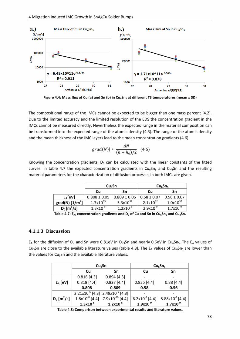
4 Migration Induced IMC Growth in SnAgCu Solder Bumps
78
Figure 4.4: Mass flux of Cu (a) and Sn (b) in Cu6Sn5 at different TS temperatures (mean ± SD)
The compositional range of the IMCs cannot be expected to be bigger than one mass percent [4.2].
Due to the limited accuracy and the limited resolution of the EDS the concentration gradient in the
IMCs cannot be measured directly. Nevertheless the expected range in the material composition can
be transformed into the expected range of the atomic density (4.3). The range of the atomic density
and the mean thickness of the IMC layers lead to the mean concentration gradients (4.6).
|"Rt$ | µ È4 & 4 /2 4.6
Knowing the concentration gradients, D0 can be calculated with the linear constants of the fitted
curves. In table 4.7 the expected concentration gradients in Cu6Sn5 and Cu3Sn and the resulting
material parameters for the characterization of diffusion processes in both IMCs are given.
Cu3Sn Cu6Sn5
Cu Sn Cu Sn
EA[eV] 0.808 ± 0.05 0.809 ± 0.05 0.58 ± 0.07 0.56 ± 0.07
grad(N) [1/m4] 1.7x1033 5.3x1032 2.1x1032 1.0x1032
D0 [m²/s] 1.3x10⁻⁸ 1.2x10⁻⁸ 2.9x10⁻⁹ 1.7x10⁻⁹ Table 4.7: EA, concentration gradients and D0 of Cu and Sn in Cu6Sn5 and Cu3Sn.
4.1.1.3 Discussion
EA for the diffusion of Cu and Sn were 0.81eV in Cu3Sn and nearly 0.6eV in Cu6Sn5. The EA values of
Cu3Sn are close to the available literature values (table 4.8). The EA values of Cu6Sn5 are lower than
the values for Cu3Sn and the available literature values.
Cu3Sn Cu6Sn5
Cu Sn Cu Sn
EA [eV]
0.816 [4.3]
0.818 [4.4]
0.808
0.894 [4.3]
0.827 [4.4]
0.809
-
0.835 [4.4]
0.58
-
0.88 [4.4]
0.56
D0 [m2/s]
2.21x10⁻⁶ [4.3]
1.8x10⁻⁸ [4.4]
1.3x10⁻⁸
2.49x10⁻⁶ [4.3]
7.9x10⁻¹⁰ [4.4]
1.2x10⁻⁸
-
6.2x10⁻⁸ [4.4]
2.9x10⁻⁹
-
5.88x10⁻⁷ [4.4]
1.7x10⁻⁹
Table 4.8: Comparison between experimental results and literature values.

4 Migration Induced IMC Growth in SnAgCu Solder Bumps
79
The main transport mechanism in the IMCs is a vacancy mechanism. The EA of the vacancy
mechanism is related to the melting temperature of the material [4.5]. The melting temperature of
Cu6Sn5 (415°C) is lower than the melting temperature of Cu3Sn (676°C) [4.6]. Hence a higher EA for
material transport in Cu3Sn can be expected. Independent of the lower EA the formation speed of
Cu6Sn5 during this investigation was not significantly faster than in previous investigations. Compared
to the literature the lower EA of this investigation is compensated by relatively low diffusion
constants.
In this investigation the D0 of Cu and Sn were found to be similar for Cu6Sn5 as well as for Cu3Sn. The
D0 of Cu and Sn in Cu6Sn5 were one order of magnitude smaller than the D0 for Cu3Sn. The D0 of Cu in
Cu3Sn was in the range of [4.4]. In this investigation the D0 of Sn in Cu3Sn was close to the Cu value,
while in [4.4] a reduced mobility of Sn in Cu3Sn was found. In [4.3] the D0 of Cu and Sn in Cu3Sn were
also similar, but both D0 values were two orders of magnitude higher than in this investigation.
In [4.4] the difference in the mobilities of Sn and Cu in Cu3Sn was explained by the difference in the
related mass fractions. Due to the relatively high Cu content in Cu3Sn the number of regular lattice
sides for Cu is higher than for Sn. Consequently a motion of Sn, without crystal deformation, would
require jumps over larger distances than for Cu. As a consequence the motion of Sn atoms would be
less probable than the motion of Cu atoms and the D0 of Sn would be lower. Nevertheless in [4.4] the
diffusion constant of Sn in Cu6Sn5 is also lower than for Cu, while their material fraction is similar.
Based on a theory of Huntington a diffusion mechanism, including crystal deformation, is given for
binary alloys [4.7]. In this case the material motion is based on a six jump motion cycle of vacancies
that allows Cu atoms to jump on to Sn lattice sides, or the other way around. In this case the
effective jump distance for Sn and Cu is the same and the D0 of Cu and Sn would be similar in Cu6Sn5
and in Cu3Sn.
Overall the similarities of D0 in [4.3] and in this investigation indicate the presence of a six jump
vacancy mechanism in the Cu-Sn IMCs. As in [4.4], also in this investigation a smaller mass flux of Sn
in Cu3Sn was found, but this is due to the lower atomic density and the smaller concentration
gradient of Sn compared to Cu.
EA can be used to define time limits for the consideration of saturation effects during the IMC
formation. Furthermore EA will be used to extrapolate the diffusion induced mass flux in the solder
joints during the TM and EM stress tests. In table 4.9 the time limits for the relevant TS test
temperatures are given. If the test time is below the calculated limit for the given test temperature
and the related IMC, the value in the table is marked green. If the test time is above the limit the
value in the table is marked red and saturation effects have to be taken into account when the
average mass flus is calculated.
Temperature: 100°C 120°C 140°C 150°C
Cu3Sn (0.8eV) 6108h 1753h 568h 336h
Cu6Sn5 (0.56eV) 2674h 1095h 487h 336h
Test time: 2798h 784h 163h 336h Table 4.9: Time limits for the consideration of saturation effects during the IMC growth.
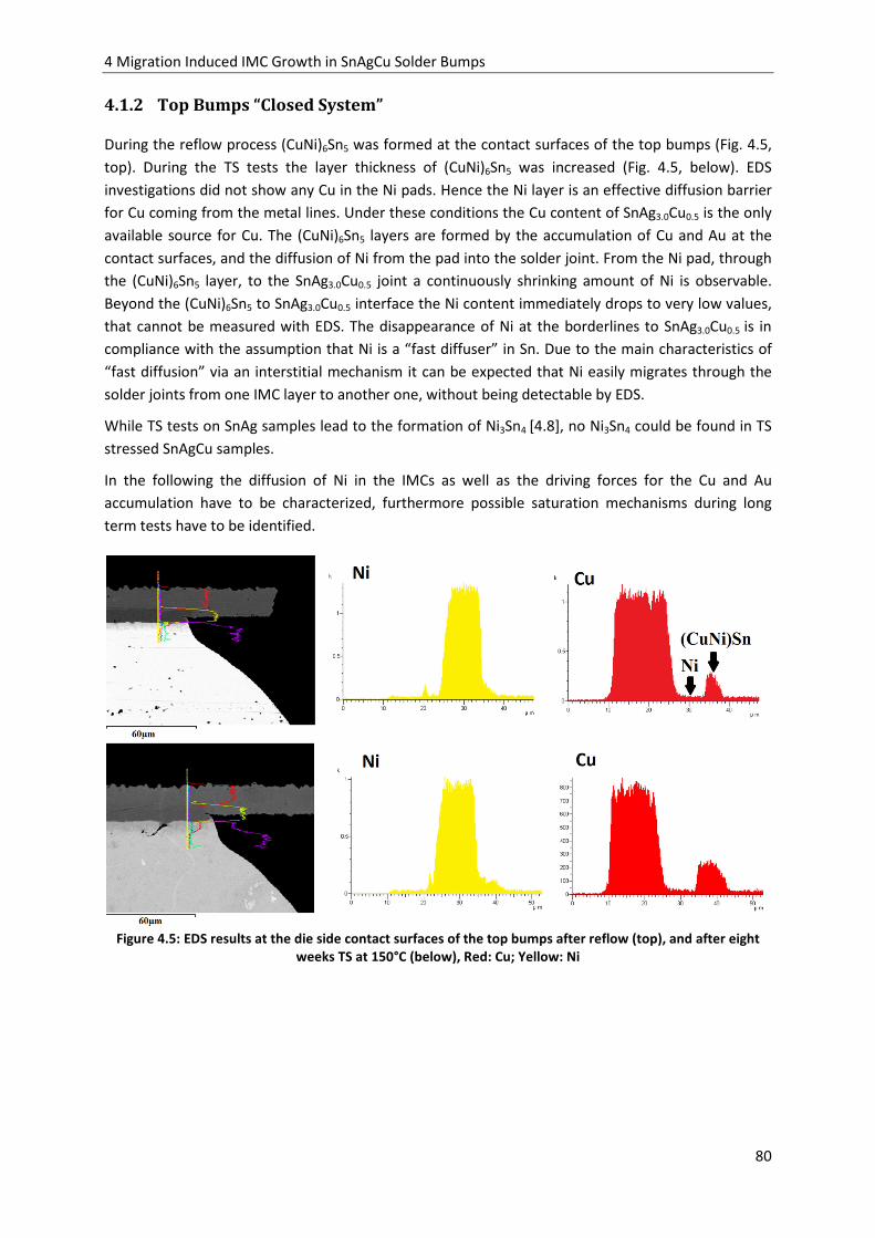
4 Migration Induced IMC Growth in SnAgCu Solder Bumps
80
4.1.2 Top Bumps “Closed System”
During the reflow process (CuNi)6Sn5 was formed at the contact surfaces of the top bumps (Fig. 4.5,
top). During the TS tests the layer thickness of (CuNi)6Sn5 was increased (Fig. 4.5, below). EDS
investigations did not show any Cu in the Ni pads. Hence the Ni layer is an effective diffusion barrier
for Cu coming from the metal lines. Under these conditions the Cu content of SnAg3.0Cu0.5 is the only
available source for Cu. The (CuNi)6Sn5 layers are formed by the accumulation of Cu and Au at the
contact surfaces, and the diffusion of Ni from the pad into the solder joint. From the Ni pad, through
the (CuNi)6Sn5 layer, to the SnAg3.0Cu0.5 joint a continuously shrinking amount of Ni is observable.
Beyond the (CuNi)6Sn5 to SnAg3.0Cu0.5 interface the Ni content immediately drops to very low values,
that cannot be measured with EDS. The disappearance of Ni at the borderlines to SnAg3.0Cu0.5 is in
compliance with the assumption that Ni is a “fast diffuser” in Sn. Due to the main characteristics of
“fast diffusion” via an interstitial mechanism it can be expected that Ni easily migrates through the
solder joints from one IMC layer to another one, without being detectable by EDS.
While TS tests on SnAg samples lead to the formation of Ni3Sn4 [4.8], no Ni3Sn4 could be found in TS
stressed SnAgCu samples.
In the following the diffusion of Ni in the IMCs as well as the driving forces for the Cu and Au
accumulation have to be characterized, furthermore possible saturation mechanisms during long
term tests have to be identified.
Figure 4.5: EDS results at the die side contact surfaces of the top bumps after reflow (top), and after eight
weeks TS at 150°C (below), Red: Cu; Yellow: Ni

4 Migration Induced IMC Growth in SnAgCu Solder Bumps
81
4.1.2.1 Long term temperature storage
During the (CuNi)6Sn5 formation Ni has to cover a growing distance before it can add to the IMC. In
addition the consumption of Cu and Au during the IMC formation reduces their concentration in the
solder joint [4.9]. As for the open system the required motion of Ni through the IMC layer leads to a
saturation effect on the (CuNi)6Sn5 formation during long term TS tests (Fig. 4.6, left). For the
(CuNi)6Sn5 formation Cu is also required and in difference to the open system the amount of available
Cu is shrinking during the IMC growth. As a consequence the fitted curve of the (CuNi)6Sn5 profile
(4.1) has a “n” value below 0.5 for the long term case. Finally the limitation of available Cu should
limit the maximum thickness of (CuNi)6Sn5 (t∞, n0) .
As for the open system the mass flux of Cu, Au and Ni in the closed system can be calculated through
the IMC growth speed, when IMC dimensions and the composition are known (4.7-8).
lmg 4 4 GD ∙ @1 mg,.mghmg,mg C ∙ 3mg,.mgh54.7
l.,J 4 4 GD ∙ 3.,J;.mgh .,J;J.54.8
Figure 4.6: TS induced (CuNi)6Sn5 growth at 150°C (a), Cu accumulation (b) [4.10]: the mass flux changes
between mode I (linear) and mode II (saturation) G=109
The composition of (CuNi)6Sn5 in the top bumps differs from the composition of the Cu-Ni-Sn IMCs on
the board side of the bottom bumps. This is due to the fact that the test board contact pads are
covered with NiP, while the contact pads in the PoP structure are covered with NiAu. The thin
(~50nm) Au layers on the Ni pads were dissolved during the reflow process and afterwards Au
accumulates in the (CuNi)6Sn5 layers. The phosphorus prevents Ni from moving into the IMC layers.
Hence the Ni content of Cu-Ni-Sn IMCs on NiAu contact pads is higher than the Ni content of IMCs on
NiP pads. Due to the presence of Cu diffusion barriers on both sides of the top bumps the Cu content
in the Cu-Ni-Sn IMCs is lower than in the bottom bumps. While the composition of the IMCs in the
bottom bumps remains the same, the TS changed the composition of the (CuNi)6Sn5 layers. The
amount of Cu and especially Au is clearly increased, while the mass fraction of Ni is reduced (table
4.10).The formation of Ni3Sn4 requires a relatively high Ni content, so taking into account the
shrinking mass fraction of Ni during TS, the missing Ni3Sn4 formation in SnAgCu solders is not
surprising anymore. As for the bottom bumps, the Ag in the top bumps forms Ag3Sn grains with the
solder. The Ag3Sn grains remain in the solder during the stress tests. Consequently no Ag was found
in the IMC layers of the top bumps.

4 Migration Induced IMC Growth in SnAgCu Solder Bumps
82
Cu Sn Ni Au
Reflow
Mass [%] 17 ± 2.0 70 ± 3.0 12.0 ± 2.4 1.0 ± 0.1
ρIMC [g/cm³] 7.8
N [1/m³] 1.25 x 1028 2.7 x 1028 9.9 x 1027 2.4 x 1026
TS
Mass [%] 19 ± 1.3 68 ± 2.0 9 ± 0.8 3.0 ± 0.7
ρIMC [g/cm³] 7.9
N [1/m³] 1.4 x 1028 2.7 x 1028 7.1 x 1027 9.6 x 1026 Table 4.10: Material composition of (CuNi)6Sn5 after reflow, and after the TS tests.
Test time [h] Reflow (0) 168 336 672 1008 1344
(CuNi)6Sn5 [µm] 1.3 ± 0.2 2.5 ± 0.4 3.0 ± 0.3 3.3 ± 0.3 3.9 ± 0.37 3.3 ± 0.65 Table 4.11: (CuNi)6Sn5 dimensions after reflow and after the TS tests.
The IMC dimensions after the short- and the long term TS tests are given in table 4.11. The saturation
effects on the (CuNi)6Sn5 lead to clear reduction of the mass flux of all three components. As a
consequence, for a test time of more than 336h, the mass flux in the IMC layers is reduced to 36% of
the starting values (table 4.12).
(CuNi)6Sn5
Test time [h] v[nm/h] JCu[1/µm²s] JNi[1/µm²s] JAu[1/µm²s]
<336h 5.4 3.9x10⁴ 1.9x10⁴ 3.5x10³
>336h 1.2 1.4x10⁴ 7.2x10³ 1.0x10³ Table 4.12: (CuNi)6Sn5 growth speed and the related mass flux during the TS tests at 150°C.
4.1.2.2 Short term temperature storage As for the open system, three short term TS test between 100°C and 140°C were performed in
addition to the TS tests at 150°C. The resulting IMC dimensions are given in table 4.13. In contrast
with to the long term TS tests the packages were soldered on a test board and two contact surfaces
per solder joint can be investigated. Compared to the results of the open system, the SDs of the
closed system are higher, because the intrinsic characteristics of the test devices (e.g. the
compositional range of SnAgCu) have a stronger influence on the IMC formation speed. The IMC
formation speed at the die side contacts was higher than at the board side contacts. The board side
results fit better to the long term results. A possible reason for the increased IMC formations speed
at the Die side contacts is a higher concentration of Cu and Au at the upper part of the solder joints.
Reflow 100°C-2798h 120°C-784h 140°C-164h
Die side (CuNi)6Sn5 [µm] 1.3 ± 0.2 2.8 ± 0.4 2.4 ± 0.3 2.8 ± 0.4
v[nm/h] - 0.54 1.4 9.1
Board side (CuNi)6Sn5 [µm] 1.25 ± 0.14 2.3 ± 0.4 1.6 ± 0.25 2.2 ± 0.3
v[nm/h] - 0.36 0.51 5.8 Table 4.13: IMC dimensions at both contact surfaces after reflow and after the TS tests.
Based on the different TS results the EA for the motion of Ni, Cu and Au were determined with a
curve fitting procedure (Fig. 4.7).

4 Migration Induced IMC Growth in SnAgCu Solder Bumps
83
Figure 4.7 Mass flux of Ni (a) [4.10] and Cu (b) in (CuNi)6Sn5 at different TS temperatures (mean ± 3*SD)
As for the bottom bumps the linear constant of the fitted Ni curve is the product of the concentration
gradient and the diffusion constant (Fig. 4.7, left). In contrast with the 1% compositional range of the
Cu-Sn IMCs in the bottom bumps, the compositional range of Ni in Cu-Ni-Sn is 100%: mNi≈100% in the
pad, and mNi≈0% in SnAgCu. This enables the direct measurement of the Ni concentration gradient in
(CuNi)6Sn5 with EDS. Afterwards D0 was calculated with (4.7).
The linear constant of the fitted Cu curve (Fig. 4.7, right) and the Au curve include the D0 of both
elements in SnAgCu and the driving forces for accumulation (β). The driving force “β” cannot be
measured directly and the extraction of D0 and β from of one experiment is impossible. Hence for Cu
and Au, literature values of D0 were used and β was extracted from the experimental results [4.11-
12]. The material parameters for the diffusion of Ni and the accumulation of Cu and Au are given in
table 4.14.
Ni Cu Au
EA[eV] 0.814-0.88 0.825-0.85 0.80-0.81
D0 [m²/s] 0.5-9.3 x 10⁻⁷ 2.4 x 10⁻⁷ [4.11] 1.6 x 10⁻⁵ [4.12]
grad(N) [1/m4] 6.9x1032 - -
β [N] - 3.6-7.8 x 10⁻¹⁶ 0.6-2.6 x 10⁻¹⁸ Table 4.14 Activation energies, concentration gradients, diffusion constants and β of Cu and Ni and Au.
4.1.2.3 Discussion
During the TS tests on the closed system the Ni pads prevent the motion of Cu from the metal lines
into the solder joints. Instead the diffusion of Ni into the solder, and the accumulation of Cu and Au,
coming from the solder led to the formation of a (CuNi)6Sn5 layer. The formation of (CuNi)3Sn was
suppressed by the relatively high Ni content [4.1]. In contrast with previous stress tests on SnAg
solders the TS did not lead to the formation of Ni3Sn4. The presence of 0.5% Cu in the SnAgCu solder
reduced the Ni consumption. As a consequence the Ni content in the IMC layers was too low for a
Ni3Sn4 formation [4.13]. The IMC growth speed in the closed system is more dependent on the
intrinsic conditions in the solder joints, than for the open system. Hence the SD of the IMC
dimensions is higher for the closed than for the open system. Against this background the extraction
of exact material parameters is more difficult than for the closed system.
EA for the motion of Cu, Ni and Au in the Cu-Ni-Sn IMCs was a round 0.8eV. The D0 of Ni in the IMCs
was relatively high compared to the mobility of Cu and Sn in the Cu-Sn IMCs of the open system.
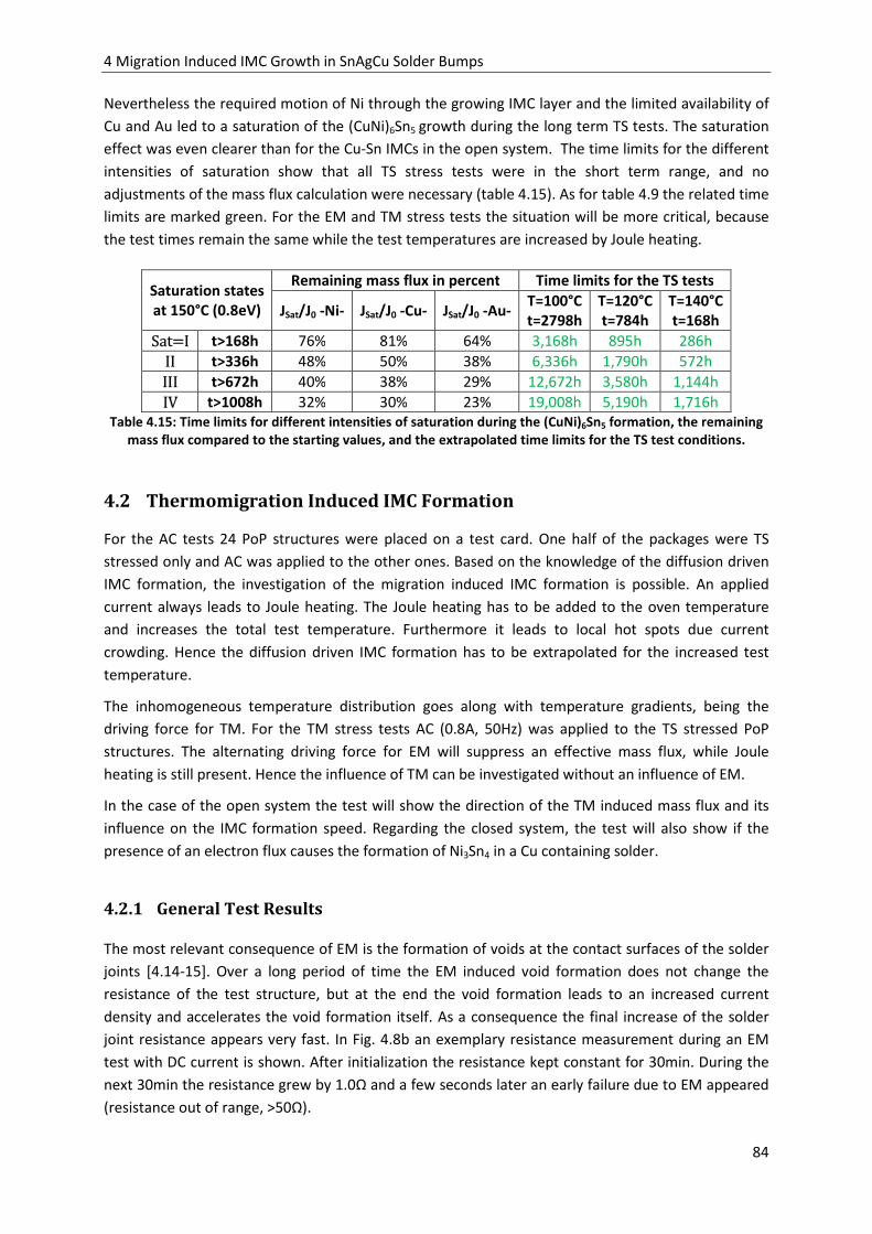
4 Migration Induced IMC Growth in SnAgCu Solder Bumps
84
Nevertheless the required motion of Ni through the growing IMC layer and the limited availability of
Cu and Au led to a saturation of the (CuNi)6Sn5 growth during the long term TS tests. The saturation
effect was even clearer than for the Cu-Sn IMCs in the open system. The time limits for the different
intensities of saturation show that all TS stress tests were in the short term range, and no
adjustments of the mass flux calculation were necessary (table 4.15). As for table 4.9 the related time
limits are marked green. For the EM and TM stress tests the situation will be more critical, because
the test times remain the same while the test temperatures are increased by Joule heating.
Saturation states
at 150°C (0.8eV)
Remaining mass flux in percent Time limits for the TS tests
JSat/J0 -Ni- JSat/J0 -Cu- JSat/J0 -Au- T=100°C
t=2798h
T=120°C
t=784h
T=140°C
t=168h
SatI t>168h 76% 81% 64% 3,168h 895h 286h
II t>336h 48% 50% 38% 6,336h 1,790h 572h
III t>672h 40% 38% 29% 12,672h 3,580h 1,144h
IV t>1008h 32% 30% 23% 19,008h 5,190h 1,716h Table 4.15: Time limits for different intensities of saturation during the (CuNi)6Sn5 formation, the remaining
mass flux compared to the starting values, and the extrapolated time limits for the TS test conditions.
4.2 Thermomigration Induced IMC Formation
For the AC tests 24 PoP structures were placed on a test card. One half of the packages were TS
stressed only and AC was applied to the other ones. Based on the knowledge of the diffusion driven
IMC formation, the investigation of the migration induced IMC formation is possible. An applied
current always leads to Joule heating. The Joule heating has to be added to the oven temperature
and increases the total test temperature. Furthermore it leads to local hot spots due current
crowding. Hence the diffusion driven IMC formation has to be extrapolated for the increased test
temperature.
The inhomogeneous temperature distribution goes along with temperature gradients, being the
driving force for TM. For the TM stress tests AC (0.8A, 50Hz) was applied to the TS stressed PoP
structures. The alternating driving force for EM will suppress an effective mass flux, while Joule
heating is still present. Hence the influence of TM can be investigated without an influence of EM.
In the case of the open system the test will show the direction of the TM induced mass flux and its
influence on the IMC formation speed. Regarding the closed system, the test will also show if the
presence of an electron flux causes the formation of Ni3Sn4 in a Cu containing solder.
4.2.1 General Test Results The most relevant consequence of EM is the formation of voids at the contact surfaces of the solder
joints [4.14-15]. Over a long period of time the EM induced void formation does not change the
resistance of the test structure, but at the end the void formation leads to an increased current
density and accelerates the void formation itself. As a consequence the final increase of the solder
joint resistance appears very fast. In Fig. 4.8b an exemplary resistance measurement during an EM
test with DC current is shown. After initialization the resistance kept constant for 30min. During the
next 30min the resistance grew by 1.0Ω and a few seconds later an early failure due to EM appeared
(resistance out of range, >50Ω).

4 Migration Induced IMC Growth in SnAgCu Solder Bumps
85
Figure 4.8: Resistance measurements during 790h AC-TM stress at 141°C (a), and one hour DC-EM stress at
178°C (b)
Even after 790h of testing the AC load did not show a significant increase of the solder joints
resistance, and no voids were found at the contact surface of the solder joints. The related resistance
measurement is shown in Fig 4.8a. The mean resistance was 19.7Ω. The noise (±0.4Ω) is due to the
test equipment, including non-shielded cables, connectors and potentiometers.
During the AC tests a thermocouple was placed on the top side of the PoP structures. The oven
temperature was 120°C and the temperature measurements show a package temperature of 141°C.
This information was used to calculate the temperature of IMC layers and their local temperature
gradients with the FEM. The simulation results show a further heating in the center of the PoP. The
IMC temperature is 145°C, so the applied current of 0.8A led to 25°C Joule heating in the IMC layers
(Fig. 4.9, left).
As a consequence of current crowding, being a well-known effect in our test structure [4.14], the
temperature gradients in the IMC layers are not homogenous.
Figure 4.9: Temperature [K] distribution in the PoP structure (left), and the temperature gradients [K/µm] in
the solder joints (right)

4 Migration Induced IMC Growth in SnAgCu Solder Bumps
86
For the further interpretation of the experimental results an average temperature gradient will be
used (4.9).
"Rt$M JÒÓ 1)Y ∙ "Rt$(Mh) ∙ )hm
h (4.9)
ASum= contact surface, N= number of finite elements, An= partial contact surface of a finite element, grad(Tn)= local temperature gradient
Previous infrared observations of solder joints have shown temperature gradients in an order of
10,000 K/m [4.16]. The maximum temperature gradients in the PoP structure appeared in the NiP
layers; they were of the order of 3000 K/m. The temperature gradients in the good thermally
conducting IMC layers are lower. The average gradients in the three relevant IMC layers are given in
table 4.16. The high thermal conductivity of Cu3Sn compared to Cu6Sn5 and (CuNi)6Sn5 leads to
smaller temperature gradients. The relatively low average temperature gradient in (CuNi)6Sn5 is a
consequence of a smaller current density, due to the larger contact surfaces of the top bumps. The
averaged gradients will be used for calculation of the Q** values. In table 4.16 also the maximum
temperature gradients are given. Due to current crowding their values are above 1000 K/m for
Cu6Sn5 and (CuNi)6Sn5.
IMC Cu3Sn Cu6Sn5 (CuNi)6Sn5
grad(T)Avg [K/m] 125 302 203
grad(T)max[K/m] 473 1049 1392 Table 4.16: Average temperature gradients in the IMC layers during the AC test.
4.2.2 Bottom Bumps “Open System” A comparison between the AC stressed and the TS stressed packages shows the influence of TM on
the IMC formation. The mean IMC dimensions of the temperature stressed and the AC stressed
packages are given in table 4.17. The test results show an accelerated IMC formation speed in the AC
stressed solder joints. Furthermore no difference between the formal upstream and the downstream
case was observable. The absence of a significant difference between the IMC growth speed for the
up- and downstream cases indicates the suppression of an EM induced IMC formation.
Test Downstream Upstream
Cu3Sn [µm] Cu6Sn5 [µm] Cu3Sn [µm] Cu6Sn5 [µm]
120°C/0 A 0.79 ± 0.1 3.52 ± 0.49
v[nm/h] 0.28 0.91
145°C/0.8 A 1.33 ± 0.13 5.6 ± 0.68 1.35 ± 0.14 5.5 ± 0.6
v[nm/h] 0.96 3.54 0.99 3.41 Table 4.17: IMC dimensions in the bottom bumps after 790h TM stress at 145°C.
Before an investigation of the TM induced mass flux is possible the diffusion due to the TS stress has
to be estimated and subtracted from the total mass flux (4.10). The diffusion induced mass flux at
120°C is known from the short term TS results. The acceleration due to Joule heating (AFT) can be
calculated with the EA taken from section 4.1.1.
l- = lY − )O ∙ l, (4.10) AF= acceleration factor
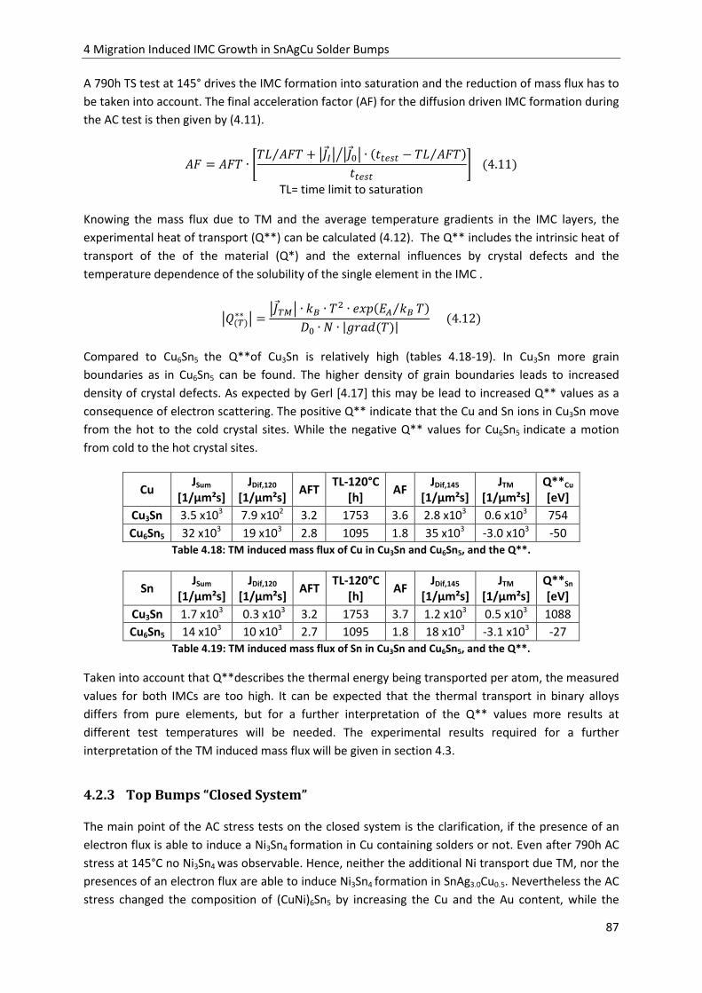
4 Migration Induced IMC Growth in SnAgCu Solder Bumps
87
A 790h TS test at 145° drives the IMC formation into saturation and the reduction of mass flux has to
be taken into account. The final acceleration factor (AF) for the diffusion driven IMC formation during
the AC test is then given by (4.11).
)O )OM ∙ »Mè )OM + l, l ∙ (GD − Mè )OM⁄ )c⁄ GD ¼ (4.11)
TL= time limit to saturation
Knowing the mass flux due to TM and the average temperature gradients in the IMC layers, the
experimental heat of transport (Q**) can be calculated (4.12). The Q** includes the intrinsic heat of
transport of the of the material (Q*) and the external influences by crystal defects and the
temperature dependence of the solubility of the single element in the IMC .
()∗∗ = l- ∙ KL ∙ M ∙ (<J KL⁄ M)6 ∙ ∙ |"Rt$(M)| (4.12)
Compared to Cu6Sn5 the Q**of Cu3Sn is relatively high (tables 4.18-19). In Cu3Sn more grain
boundaries as in Cu6Sn5 can be found. The higher density of grain boundaries leads to increased
density of crystal defects. As expected by Gerl [4.17] this may be lead to increased Q** values as a
consequence of electron scattering. The positive Q** indicate that the Cu and Sn ions in Cu3Sn move
from the hot to the cold crystal sites. While the negative Q** values for Cu6Sn5 indicate a motion
from cold to the hot crystal sites.
Cu JSum
[1/µm²s]
JDif,120
[1/µm²s] AFT TL-120°C
[h] AF
JDif,145
[1/µm²s]
JTM
[1/µm²s]
Q**Cu
[eV]
Cu3Sn 3.5 x10³ 7.9 x10² 3.2 1753 3.6 2.8 x10³ 0.6 x10³ 754
Cu6Sn5 32 x103 19 x103 2.8 1095 1.8 35 x103 -3.0 x10³ -50
Table 4.18: TM induced mass flux of Cu in Cu3Sn and Cu6Sn5, and the Q**.
Sn JSum
[1/µm²s]
JDif,120
[1/µm²s] AFT TL-120°C
[h] AF
JDif,145
[1/µm²s]
JTM
[1/µm²s]
Q**Sn
[eV]
Cu3Sn 1.7 x10³ 0.3 x10³ 3.2 1753 3.7 1.2 x10³ 0.5 x10³ 1088
Cu6Sn5 14 x103 10 x103 2.7 1095 1.8 18 x103 -3.1 x10³ -27
Table 4.19: TM induced mass flux of Sn in Cu3Sn and Cu6Sn5, and the Q**.
Taken into account that Q**describes the thermal energy being transported per atom, the measured
values for both IMCs are too high. It can be expected that the thermal transport in binary alloys
differs from pure elements, but for a further interpretation of the Q** values more results at
different test temperatures will be needed. The experimental results required for a further
interpretation of the TM induced mass flux will be given in section 4.3.
4.2.3 Top Bumps “Closed System”
The main point of the AC stress tests on the closed system is the clarification, if the presence of an
electron flux is able to induce a Ni3Sn4 formation in Cu containing solders or not. Even after 790h AC
stress at 145°C no Ni3Sn4 was observable. Hence, neither the additional Ni transport due TM, nor the
presences of an electron flux are able to induce Ni3Sn4 formation in SnAg3.0Cu0.5. Nevertheless the AC
stress changed the composition of (CuNi)6Sn5 by increasing the Cu and the Au content, while the
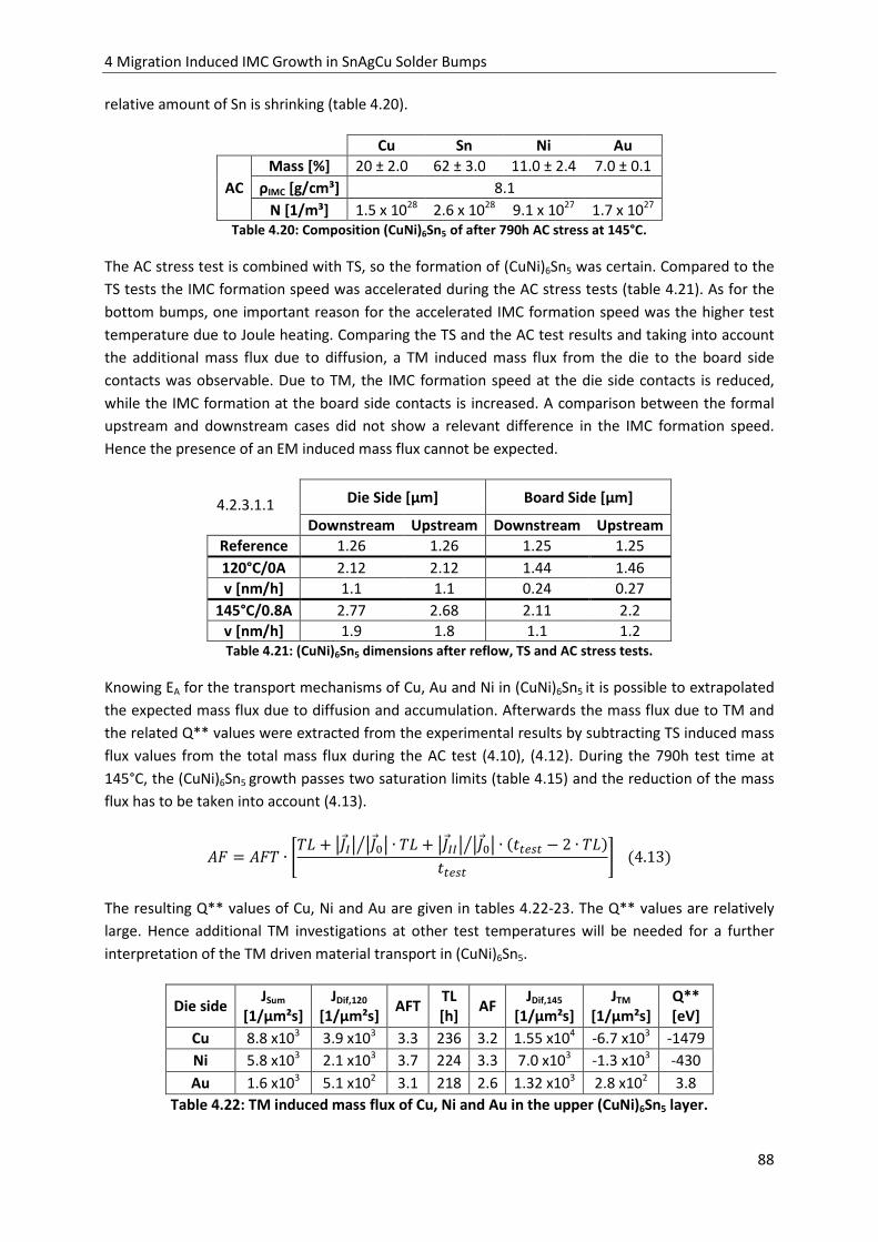
4 Migration Induced IMC Growth in SnAgCu Solder Bumps
88
relative amount of Sn is shrinking (table 4.20).
Cu Sn Ni Au
AC
Mass [%] 20 ± 2.0 62 ± 3.0 11.0 ± 2.4 7.0 ± 0.1
ρIMC [g/cm³] 8.1
N [1/m³] 1.5 x 1028 2.6 x 1028 9.1 x 1027 1.7 x 1027 Table 4.20: Composition (CuNi)6Sn5 of after 790h AC stress at 145°C.
The AC stress test is combined with TS, so the formation of (CuNi)6Sn5 was certain. Compared to the
TS tests the IMC formation speed was accelerated during the AC stress tests (table 4.21). As for the
bottom bumps, one important reason for the accelerated IMC formation speed was the higher test
temperature due to Joule heating. Comparing the TS and the AC test results and taking into account
the additional mass flux due to diffusion, a TM induced mass flux from the die to the board side
contacts was observable. Due to TM, the IMC formation speed at the die side contacts is reduced,
while the IMC formation at the board side contacts is increased. A comparison between the formal
upstream and downstream cases did not show a relevant difference in the IMC formation speed.
Hence the presence of an EM induced mass flux cannot be expected.
4.2.3.1.1 Die Side [µm] Board Side [µm]
Downstream Upstream Downstream Upstream
Reference 1.26 1.26 1.25 1.25
120°C/0A 2.12 2.12 1.44 1.46
v [nm/h] 1.1 1.1 0.24 0.27
145°C/0.8A 2.77 2.68 2.11 2.2
v [nm/h] 1.9 1.8 1.1 1.2 Table 4.21: (CuNi)6Sn5 dimensions after reflow, TS and AC stress tests.
Knowing EA for the transport mechanisms of Cu, Au and Ni in (CuNi)6Sn5 it is possible to extrapolated
the expected mass flux due to diffusion and accumulation. Afterwards the mass flux due to TM and
the related Q** values were extracted from the experimental results by subtracting TS induced mass
flux values from the total mass flux during the AC test (4.10), (4.12). During the 790h test time at
145°C, the (CuNi)6Sn5 growth passes two saturation limits (table 4.15) and the reduction of the mass
flux has to be taken into account (4.13).
)O )OM ∙ »Mè + l, lc ∙ Mè + l,, lc ∙ (GD − 2 ∙ Mè)GD ¼ (4.13)
The resulting Q** values of Cu, Ni and Au are given in tables 4.22-23. The Q** values are relatively
large. Hence additional TM investigations at other test temperatures will be needed for a further
interpretation of the TM driven material transport in (CuNi)6Sn5.
Die side JSum
[1/µm²s]
JDif,120
[1/µm²s] AFT TL
[h] AF
JDif,145
[1/µm²s]
JTM
[1/µm²s]
Q**
[eV]
Cu 8.8 x10³ 3.9 x10³ 3.3 236 3.2 1.55 x10⁴ -6.7 x10³ -1479
Ni 5.8 x10³ 2.1 x10³ 3.7 224 3.3 7.0 x10³ -1.3 x10³ -430
Au 1.6 x10³ 5.1 x10² 3.1 218 2.6 1.32 x10³ 2.8 x10² 3.8
Table 4.22: TM induced mass flux of Cu, Ni and Au in the upper (CuNi)6Sn5 layer.

4 Migration Induced IMC Growth in SnAgCu Solder Bumps
89
Board side JSum
[1/µm²s]
JDif,120
[1/µm²s] AFT TL-1
[h] AF
JDif,145
[1/µm²s]
JTM
[1/µm²s]
Q**
[eV]
Cu 6.3 x10³ 1.6 x10³ 3.5 221 3.2 5.1 x10³ 1.3 x10³ -519
Ni 2.7 x10³ 7.9 x10² 3.2 218 2.9 2.3 x10³ 3.3 x10² -299
Au 1.22 x10³ 3.97 x10² 3.2 218 2.59 1.28 x10³ -0.6 x10² 3.3
Table 4.23: TM induced mass flux of Cu, Ni and Au in the lower (CuNi)6Sn5 layer.
4.2.4 Conclusion During the AC stress tests no void formation and no migration induced failure of the bump chains
were observable. In the top- or bottom bumps no difference in the IMC formation speed was
observable for the formal up- or downstream case. Hence it can be assumed that the chosen
frequency of 50Hz was high enough to suppress an effective mass flux due to EM.
The applied current of 0.8A led to 25°C Joule heating and current crowding appeared at the corners
of the solder joints. The combination of Joule heating and current crowding led to an inhomogeneous
temperature distribution in the solder joints. The resulting temperature gradients are a driving force
for TM.
The presence of TM in the IMCs had a clear influence on the IMC formation speed in the top and the
bottom bumps. Nevertheless the influence of TM was not strong enough to induce a Ni3Sn4
formation in SnAg3.0Cu0.5. As a consequence only a directed mass flux due to EM can expected to be a
possible driving force for the Ni3Sn4 formation in Cu containing solders.
With the EA of the different transport mechanism for Cu, Sn, Ni and Au in the IMC layers it was
possible to predict the influence of diffusion and material accumulation on the AC test results.
Afterwards the extraction of the TM induced mass flux was possible. Knowing the TM induced mass
flux and the temperature gradients the Q** values were extracted.
The single Q** values of Cu and Sn in Cu3Sn and Cu6Sn5 and of Cu, Ni and Au in (CuNi)6Sn5 were
calculated. Nevertheless one data point does not allow a further interpretation of the TM driven
material transport in binary or even more complex alloys. Hence the presence of TM during the DC
tests will be used for an extraction of three additional Q** values at different test temperatures.

4 Migration Induced IMC Growth in SnAgCu Solder Bumps
90
4.3 Electromigration Induced IMC Formation
The EM tests were performed at three different oven temperatures: 100°C, 120°C and 140°C. For the
EM tests the TS is combined with a DC of 1A. During the DC tests, diffusion, material accumulation,
TM and EM appeared. The DC tests are close to the use case of BGAs and they can be used to
simulate a migration accelerated TLPS process. For the interpretation of the DC test results, the
previous test results from the TS and the AC stress tests are relevant. Furthermore EM is able to
induce Ni3Sn4 formation in Cu containing solders.
4.3.1 General Test Results
The applied current of 1A leads to Joule heating. Hence the test temperature is higher than the
chosen oven temperature. As for the AC tests thermocouples were used for temperature
measurements, being the boundary conditions for a FEA. The test temperatures at the IMC layers
are: 138°C, 161°C and 185°C. Hence Joule heating increased the test temperature by +38°C from
100°C, and by +45°C from 140°C. The reason for more Joule heating at higher oven temperatures is a
higher specific resistance of the metal lines and the solder joints. While the resistance of the bump
chain was increased due to the rising temperature a LabView® program increased the voltage to
keep a constant current of 1A. By that way the applied electrical power was also increased.
As for AC tests the DC tests are also influenced by current crowding (Fig. 4.10). The consequences are
temperature gradients in the solder joints and in the IMC layers (table 4.24), as well as mass flux
divergences of the EM (3.24).
Figure 4.10: Current density [A/µm²] (left) and temperature gradient distribution [K/µm] at the die side
contact surfaces of the top solder joints (right) [4.10]
Ttest [°C] Cu3Sn [K/m] Cu6Sn5 [K/m] (CuNi)6Sn5 [K/m] Ni3Sn4 [K/m]
avg max avg max avg max avg max
138 195 601 509 1435 293 1627 297 2520
161 220 663 575 1605 313 1576 313 2377
185 247 659 636 1599 344 1739 344 2655 Table 4.24: Averaged and maximum temperature gradients in the IMC layers.
In contrast with the AC tests, the DC tests led to an effective mass flux by EM. The divergences of the
EM induced mass flux led to migration induced void formation (Fig. 4.11). Hence the EM DC tests can
lead to failures of the bump chain, while the TS or AC tests cannot.

4 Migration Induced IMC Growth in SnAgCu Solder Bumps
91
Figure 4.11: EM induced void formation as consequence of current crowding at the top bump (left) and the
bottom bump contact surfaces (right) [4.18]
4.3.2 Bottom Bumps “Open System”
For both the AC and the DC experiments, test cards with 24 PoP structures were used. One half of
the packages were TS stressed only, the others were TS and DC stressed. Afterwards the IMC
dimensions of the DC stressed and TS stressed packages were compared.
4.3.2.1 Parameter extraction Compared to the TS tests the formation speeds of Cu6Sn5 and Cu3Sn were increased (table 4.25). One
reason for the accelerated IMC formation is Joule heating and the resulting difference in the test
temperatures for the TS and the EM tests.
In contrast with the AC tests, DC stress led to different results for the up- and the downstream cases.
The IMC formation speeds of Cu6Sn5 and Cu3Sn were accelerated for the upstream and decelerated
for the downstream case. In all cases at the board side contact surfaces only a thin (CuNi)6Sn5 layer
was observable. Hence the presence of phosphorus in the Ni pad suppressed the Ni3Sn4 formation,
even under DC stress at 185°C.
Upstream Downstream
Test Surface Cu3Sn [µm] Cu6Sn5 [µm] Cu3Sn [µm] Cu6Sn5 [µm]
138°C/1 A
2369 h
Upper 1.15 ± 0.1 6.4 ± 1.0 1.34 ± 0.17 8.7 ± 0.73
Lower - 3.2 ± 0.6 - 2.9 ± 0.5
161°C/1 A
192 h
Upper 1.5 ± 0.34 6.9 ± 1.1 1.6 ± 0.24 8.8 ± 1.25
Lower - 3.5 ± 1.14 - 3.1 ± 0.8
185°C/1 A
144 h
Upper 1.6 ± 0.4 9.67 ± 1.87 2.0 ± 0.32 11.4 ± 2.4
Lower - 7.4 ± 1.4 - 6.6 ± 1.7
Table 4.25: Cu3Sn and Cu6Sn5 dimensions after the EM stress tests.
As a consequence of current crowding the IMC formation speed at the corners of the solder joints
should differ from the IMC formation speed at the center of the solder joints. The direct observation
of EM by current crowding was difficult: the upstream case led to relatively homogenous IMC layers
(Fig. 4.12, left), while the current crowding induced degradation of the IMC layer (Fig 4.12, right)
became visible for the upstream case. The reason why the IMC formation in the bottom bumps was
not clearly affected by current crowding has to be clarified with FEA (chapter 5).

4 Migration Induced IMC Growth in SnAgCu Solder Bumps
92
Figure 4.12: IMC layers at the die sided contact surfaces of a downstream (left) and an upstream stressed
(right) bump after 2769h EM at 138°C
As a consequence of the missing current crowding effect on the IMC formation, statistics were used
to clarify the influence of EM on the IMC formation speed for the up- and downstream cases (Fig.
4.13).
Figure 4.13: Box plots of the IMC dimensions after the up- and downstream EM stress tests for three
different test temperatures
The extraction of the EM induced mass flux was done by comparing the up- and downstream cases
(4.14). The benefit of this method is the fact that no extrapolation of the diffusion induced mass flux
is necessary. Due to Joule heating, an extrapolation of the diffusion induced mass flux was necessary
for the extraction of the TM induced mass flux (4.15).
lU- l,~Éh l,ÊV2 4.14 l- 3l,~Éh & l,ÊV52 l, l,. 4.15 The EM DC tests are life time tests and downtimes without Joule heating appeared, because bump
chains failed due to void formation. Afterwards the system had to be reset. During the resulting
downtimes only a diffusion driven mass flux at the oven temperature appeared in the formally DC
stressed solder joints. The mass flux during the downtimes was taken into account by transforming
the AF (4.11) to AF* (4.16).
)O∗ )O ∙ Ë1 & I .)O ∙ . NÌ4.16 tTS= total test time including all downtimes, tDC= test time without downtimes
The resulting mass flux values of Sn and Cu in Cu3Sn and Cu6Sn5 are given in the tables 4.26-29. In
Cu3Sn the TM induced mass flux is higher than the EM induced mass flux. In the Cu6Sn5 layer both
kinds of migration lead to similar math flux values. The relatively high TM values in both IMCs have to
be explained by a further analysis of the test results.

4 Migration Induced IMC Growth in SnAgCu Solder Bumps
93
Cu3Sn
-Cu-
JDown
[1/µm²s]
JUp
[1/µm²s]
JEM,Cu
[1/µm²s]
JDif,TS
[1/µm²s] AFT TL
[h] AF AF*
JDif,DC-EM
[1/µm²s]
JTM,Cu
[1/µm²s]
138°C 1.2 x10³ 0.75 x10³ 0.24 x10³ 0.1 x10³ 10 646 8.0 8.2 0.8 x10³ 0.2 x10³
161°C 22 x103 20 x103 1.0 x10³ 1.3 x10³ 9.5 192 9.5 12 16 x103 3.9 x10³
185°C 34 x103 26 x103 3.0 x10³ 2.4 x10³ 9.3 62 7.7 7.8 19 x103 11 x103
Table 4.26: Total mass flux during the up- and downstream tests, the mass flux due to EM, the diffusion
induced mass flux, the AFs and the TM induced mass flux. All values for Cu in Cu3Sn.
Cu3Sn
-Sn-
JDown
[1/µm²s]
JUp
[1/µm²s]
JEM,Sn
[1/µm²s]
JDif,TS
[1/µm²s] AFT TL
[h] AF AF*
JDif,DC-EM
[1/µm²s]
JTM,Sn
[1/µm²s]
138°C 0.5 x10³ 0.3 x10³ 0.1 x10³ 0.4 x10² 10 646 8.0 8.2 0.3 x10³ 0.1 x10³
161°C 8.9 x10³ 8.1 x10³ 0.4 x10³ 0.5 x10³ 9.5 192 9.5 12 6.2 x10³ 2.0 x10³
185°C 14 x103 11 x103 1.7 x10³ 1.0 x10³ 9.3 62 7.7 7.8 7.8 x10³ 3.4 x10³
Table 4.27: Total mass flux during the up- and downstream tests, the mass flux due to EM, the diffusion
induced mass flux, the AFs and the TM induced mass flux. All values for Sn in Cu3Sn.
Cu6Sn5
-Cu-
JDown
[1/µm²s]
JUp
[1/µm²s]
JEM,Cu
[1/µm²s]
JDif,TS
[1/µm²s] AFT TL
[h] AF AF*
JDif,DC-EM
[1/µm²s]
JTM,Cu
[1/µm²s]
138°C 21 x103 13 x103 3.7 x 10³ 10 x103 5.2 533 2.0 2.2 22 x103 -5.2 x10³
161°C 2.6 x10⁵ 1.9 x10⁵ 37 x103 31 x103 5.0 225 5.0 8.1 2.5 x10⁵ -25 x103
185°C 5.5 x10⁵ 3.4 x10⁵ 1.1 x10⁵ 1.2 x10⁵ 3.9 100 3.7 3.0 5.0 x10⁵ -53 x103
Table 4.28: Total mass flux during the up- and downstream tests, the mass flux due to EM, the diffusion
induced mass flux, the AFs and the TM induced mass flux. All values for Cu in Cu6Sn5.
Cu6Sn5
-Sn-
JDown
[1/µm²s]
JUp
[1/µm²s]
JEM,Sn
[1/µm²s]
JDif,TS
[1/µm²s] AFT TL
[h] AF AF*
JDif,DC-EM
[1/µm²s]
JTM,Sn
[1/µm²s]
138°C 8.8 x10³ 5.8x10³ 1.4 x10³ 3.2 x10³ 5.0 525 2.3 2.5 10 x103 -2.0 x10³
161°C 1.1 x10⁵ 0.8 x10⁵ 16 x103 13 x103 3.8 227 3.8 7.9 1.0 x10⁵ -5.9 x10³
185°C 2.4 x10⁵ 1.5 x10⁵ 37 x103 54 x103 3.7 104 3.8 3.9 2.1 x10⁵ -11 x103
Table 4.29: Total mass flux during the up- and downstream tests, the mass flux due to EM, the diffusion
induced mass flux, the AFs and the TM induced mass flux. All values for Sn in Cu6Sn5.
The extracted mass flux values of the EM and TM during the DC tests enabled the calculation of the
related Z** (4.17) and Q** (4.12) values. The results are given in table 4.30. For the calculation of Z**
the specific resistances of the IMCs and their TCRs have to be known. The specific resistances of
Cu3Sn and Cu6Sn5 are available in the literature, but a TCR is only available for Cu6Sn5 (table 3.1).
Hence the Z** values were calculated with a temperature independent specific resistance. The
consequence is a temperature dependency of the Z** values. The Q** values are regularly
temperature dependent.
o ∗∗ = lU- ∙ KL ∙ M ∙ (<J KL⁄ M)6 ∙ ∙ |f| ∙ ∙ Gq (4.17)
Cu3Sn Cu6Sn5
Cu Sn Cu Sn
Ttest [°C] Z** Q**[eV] Z** Q**[eV] Z** Q**[eV] Z** Q**[eV]
138 29 908 56 1115 14 -50 6 -20
161 45 645 71 665 28 -43 15 -13
185 61 491 84 68 37 -38 16 -11 Table 4.30: Z** and Q** values of Cu and Sn in Cu3Sn and Cu6Sn5.

4 Migration Induced IMC Growth in SnAgCu Solder Bumps
94
4.3.2.2 Discussion
The DC tests reproduced the Q** values of the AC test. Nevertheless all Q** and Z** values are too
high for single ions, and they are strongly temperature dependent. The equations being used for the
calculation of Z** and Q** are appropriate for metals with a fcc crystal structure. The main
difference between the IMCs and an idealized fcc structure is the presence of grain boundaries. The
presence of grain boundaries leads to a high defect density. Hence the interpretation of the
extracted Z** values has to be done under consideration of electron scattering at crystal defects.
In metals, heat transmission is mainly influenced by the electron gas. Hence electron scattering in the
IMC does not only lead to increased Z** values, it also leads to high Q** values. As a consequence of
smaller grains and a higher density of grain boundaries the Q** values of Cu3Sn were relatively large
compared to Cu6Sn5.
A model for the determination of temperature independent Z* under consideration of crystal defects
is given by Bosvieux and Friedel (4.18). More details are available in section 3.2.2.
o∗∗() = 12 ∙ o ∙ I1 − ∙ ∙ N + 2®()3b o ∙ @l I tRN − 2l I tRNC (3.35/4.18)
The Bohr radius (rH) of the elements, the lattice constants of the IMCs (a) and the results of the
Bessel functions are given table 4.31. All results of the Bessel functions are negative.
b [nm] rH-Cu [nm] rH-Sn [nm] (J0-2J2) -Cu- (J0-2J2) -Sn-
Cu3Sn 0.56 0.128 0.145 -0.86 -1,2
Cu6Sn5 0.5 0.128 0.145 -1.17 -1.3 Table 4.31: Result of the Bessel functions for Cu and Sn in Cu3Sn and Cu6Sn5.
The Z** values depend on the average lifetime of the moving electrons (τ). Furthermore the TCRs of
the IMCs were not taken into account. The result is a nonlinear temperature dependence of Z**.
In the following most of the material parameters in (4.18) will be summarized in Z*. The nonlinear
part of (4.19) is related the to influence of the electron’s lifetime, also being the main part of the
TCR. The linear part (α) of (4.19) is related to the temperature dependence of the relative defect
density (1-NρD/NDρ). Due to the negative results of the Bessel functions the nonlinear part of (4.19) is
negative too.
o()∗∗ = o∗ ∙ 1 + ∙ (M − 300W) − o∗ ∙ 1 + M!s ∙ (M − 300W) (4.19)
By curve fitting the data points of Z** (Fig. 4.14) the TCR, α and Z* can be approximated through the
linear terms (A, B, C) of the trend line (4.20).
o()∗∗ = −!∆M + P∆M + ) (4.20)
The term A, includes Z* (4.21). The terms C and B include the TCR (4.22) and α (4.23).
o(,)∗ = 0.5 ± `(0.25) − ) (4.21) M!s = `−! o∗⁄ (4.22)
= P + 2 ∙ o∗ ∙ M!so∗ (4.23)
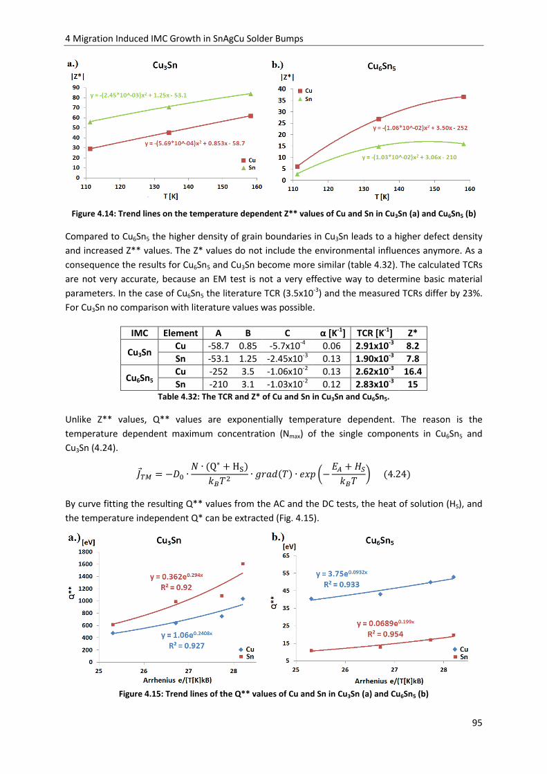
4 Migration Induced IMC Growth in SnAgCu Solder Bumps
95
Figure 4.14: Trend lines on the temperature dependent Z** values of Cu and Sn in Cu3Sn (a) and Cu6Sn5 (b)
Compared to Cu6Sn5 the higher density of grain boundaries in Cu3Sn leads to a higher defect density
and increased Z** values. The Z* values do not include the environmental influences anymore. As a
consequence the results for Cu6Sn5 and Cu3Sn become more similar (table 4.32). The calculated TCRs
are not very accurate, because an EM test is not a very effective way to determine basic material
parameters. In the case of Cu6Sn5 the literature TCR (3.5x10⁻³) and the measured TCRs differ by 23%.
For Cu3Sn no comparison with literature values was possible.
IMC Element A B C α [K-1] TCR [K-1] Z*
Cu3Sn Cu -58.7 0.85 -5.7x10⁻⁴ 0.06 2.91x10⁻³ 8.2
Sn -53.1 1.25 -2.45x10⁻³ 0.13 1.90x10⁻³ 7.8
Cu6Sn5 Cu -252 3.5 -1.06x10⁻² 0.13 2.62x10⁻³ 16.4
Sn -210 3.1 -1.03x10⁻² 0.12 2.83x10⁻³ 15
Table 4.32: The TCR and Z* of Cu and Sn in Cu3Sn and Cu6Sn5.
Unlike Z** values, Q** values are exponentially temperature dependent. The reason is the
temperature dependent maximum concentration (Nmax) of the single components in Cu6Sn5 and
Cu3Sn (4.24).
l- 6 ∙ ∙ Q∗ & H· KLM ∙ "Rt$M ∙ I <J & [KLM N 4.24
By curve fitting the resulting Q** values from the AC and the DC tests, the heat of solution (HS), and
the temperature independent Q* can be extracted (Fig. 4.15).
Figure 4.15: Trend lines of the Q** values of Cu and Sn in Cu3Sn (a) and Cu6Sn5 (b)

4 Migration Induced IMC Growth in SnAgCu Solder Bumps
96
Taking into account the temperature dependent solubility of single components in the binary IMCs,
the resulting Q* values for Cu and Sn are closer to the expected range, being defined by the physical
model of thermomigration (table 4.33). Furthermore the results for Cu3Sn and Cu6Sn5 do not differ by
two orders anymore. Compared to the Q* values of Cu, the Q* values of Sn in both IMCs are
relatively small.
IMC Element EA,Dif [eV] H [eV] EA,TM = (EA + HS) [eV] Q* + HS [eV] Q* [eV]
Cu3Sn Cu 0.81 -0.24 0.57 1.1 1.34
Sn 0.81 -0.29 0.52 0.36 0.65
Cu6Sn5 Cu 0.58 -0.09 0.49 -3.75 -3.7
Sn 0.56 -0.2 0.36 -0.07 0.13
Table 4.33: The HS and the Q* values of Cu and Sn in Cu3Sn and Cu6Sn5.
4.3.3 Top Bumps “Closed System” As for the open system, the results of the DC stress tests of the closed system were extracted by
comparing the DC and the TS test results. Afterwards the Q** and Z** values were calculated
through the related mass flux values of TM and EM. Finally a physical interpretation of the material
values is needed.
4.3.3.1 Parameter extraction
The presence of a non-alternating current flow leads to the formation of Ni3Sn4 in the SnAgCu solder
joints. Furthermore a (CuNi)6Sn5 layer is formed. The resulting IMC layer dimensions at the die and
the board side contact surfaces are given in the tables 4.34-35. The influence of the current flow on
the two different IMC layers is different. As in [4.8], and in contrast with [4.9], the direction of the
current flow had no significant influence on the Ni3Sn4 formation speed. Following the interpretation
of [4.8] a possible reason for the missing influence of the current direction is an equal exchange of Ni
and Sn at the Ni3Sn4 to Ni interface.
(CuNi)6Sn5 [µm] Ni3Sn4 [µm]
Down Up Down Up
138°C/1A 3.85±0.44 3.98±0.8 1.14±0.36 1.33±0.37
161°C/1A 3.84±1.25 6.47±0.9 2.94±0.58 2.64±0.48
185°C/1A 3.86±1.17 6.08±0.65 3.02±0.18 3.5±1.1 Table 4.34: IMC dimensions and the SD at the die side contacts after the EM stress tests.
(CuNi)6Sn5 [µm] Ni3Sn4 [µm]
Down Up Down Up
138°C/1A 3.39±0.87 3.9±0.8 1.26±0.5 1.74±0.9
161°C/1A 5.0±0.53 3.29±0.73 3.93±0.92 3.83±1.0
185°C/1A 5.28±0.74 3.57±0.89 5.17±0.71 5.0±0.46 Table 4.35: IMC dimensions and the SD at the board side contacts after the EM stress tests.
The direction of the current flow has a clear influence on the (CuNi)6Sn5 growth speed. The main
reason is the NiAu diffusion barrier: e.g. for the downstream case Cu is moving, via interstitial
diffusion, from the die side contact surfaces to the board side ones. The missing Cu from the die side
accumulates at the board side and cannot be replaced by Cu from the metal lines. In the upstream

4 Migration Induced IMC Growth in SnAgCu Solder Bumps
97
case the same effect appears in an opposite direction. In combination with current crowding the
disappearance of Cu did not only reduce the (CuNi)6Sn5 formation speed, it led to a complete
dissolution of the (CuNi)6Sn5 layer (Fig. 4.16). This also led to a relatively high SD of the (CuNi)6Sn5
dimensions for the downstream case on the die side, or for the upstream case at the board side.
Figure 4.16: IMCs at the contact surfaces of a top bump after 144h DC stress at 185°C [4.10]
As the AC test the DC tests also changed the composition of (CuNi)6Sn5 (table 4.36). In addition the
composition of Ni3Sn4 had to be investigated (table 4.37). Compared to the TS or the AC tests the
amount of Ni in (CuNi)6Sn5 was increased. The mass fractions of Au and Cu are nearly the same.
Cu Sn Ni Au
(CuNi)6Sn5
Mass [%] 19 ± 1.3 60 ± 2.0 12.5 ± 0.8 7.5 ± 0.7
ρIMC [g/cm³] 8.2
N [1/m³] 1.4 x 1028 2.5 x 1028 1.1 x 1028 2.1 x 1027 Table 4.36: Material composition of (CuNi)6Sn5 after the EM stress tests.
Cu Sn Ni Au
Ni3Sn4
Mass [%] 5 ± 0.8 73 ± 1.0 22 ± 1.4 0
ρIMC [g/cm³] 7.7
N [1/m³] 3.6 x 1027 2.8 x 1028 1.7 x 1028 0 Table 4.37: Material composition of Ni3Sn4 after the EM stress tests.
The EM induced mass flux leads to an increasing amount of Ni in (CuNi)6Sn5. If an atomic
concentration of 25% is reached, the (CuNi)6Sn5 in transformed into Ni3Sn4 (Fig. 4.17). During this
process the Au vanishes and the Cu content is reduced to a few mass percent.
Figure 4.17: Material composition of the die side contact surface of a TS top bump (a) and the board side of a
EM stressed top bump (b) [4.20]
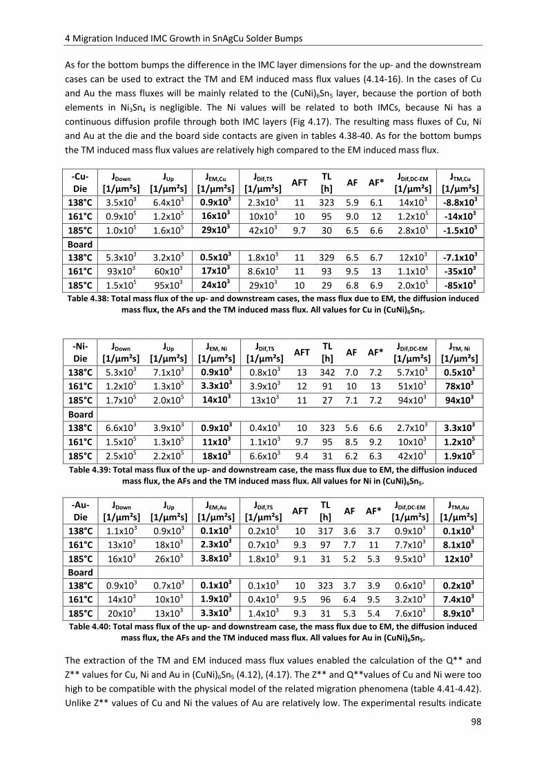
4 Migration Induced IMC Growth in SnAgCu Solder Bumps
98
As for the bottom bumps the difference in the IMC layer dimensions for the up- and the downstream
cases can be used to extract the TM and EM induced mass flux values (4.14-16). In the cases of Cu
and Au the mass fluxes will be mainly related to the (CuNi)6Sn5 layer, because the portion of both
elements in Ni3Sn4 is negligible. The Ni values will be related to both IMCs, because Ni has a
continuous diffusion profile through both IMC layers (Fig 4.17). The resulting mass fluxes of Cu, Ni
and Au at the die and the board side contacts are given in tables 4.38-40. As for the bottom bumps
the TM induced mass flux values are relatively high compared to the EM induced mass flux.
-Cu-
Die
JDown
[1/µm²s]
JUp
[1/µm²s]
JEM,Cu
[1/µm²s]
JDif,TS
[1/µm²s] AFT TL
[h] AF AF*
JDif,DC-EM
[1/µm²s]
JTM,Cu
[1/µm²s]
138°C 3.5x10³ 6.4x10³ 0.9x10³ 2.3x10³ 11 323 5.9 6.1 14x103 -8.8x10³
161°C 0.9x10⁵ 1.2x10⁵ 16x103 10x103 10 95 9.0 12 1.2x10⁵ -14x103
185°C 1.0x10⁵ 1.6x10⁵ 29x103 42x103 9.7 30 6.5 6.6 2.8x10⁵ -1.5x10⁵
Board
138°C 5.3x10³ 3.2x10³ 0.5x10³ 1.8x10³ 11 329 6.5 6.7 12x103 -7.1x10³
161°C 93x103 60x103 17x103 8.6x10³ 11 93 9.5 13 1.1x10⁵ -35x103
185°C 1.5x10⁵ 95x103 24x103 29x103 10 29 6.8 6.9 2.0x10⁵ -85x103
Table 4.38: Total mass flux of the up- and downstream cases, the mass flux due to EM, the diffusion induced
mass flux, the AFs and the TM induced mass flux. All values for Cu in (CuNi)6Sn5.
-Ni-
Die
JDown
[1/µm²s]
JUp
[1/µm²s]
JEM, Ni
[1/µm²s]
JDif,TS
[1/µm²s] AFT TL
[h] AF AF*
JDif,DC-EM
[1/µm²s]
JTM, Ni
[1/µm²s]
138°C 5.3x10³ 7.1x10³ 0.9x10³ 0.8x10³ 13 342 7.0 7.2 5.7x10³ 0.5x10³
161°C 1.2x10⁵ 1.3x10⁵ 3.3x10³ 3.9x10³ 12 91 10 13 51x103 78x103
185°C 1.7x10⁵ 2.0x10⁵ 14x103 13x103 11 27 7.1 7.2 94x103 94x103
Board
138°C 6.6x10³ 3.9x10³ 0.9x10³ 0.4x10³ 10 323 5.6 6.6 2.7x10³ 3.3x10³
161°C 1.5x10⁵ 1.3x10⁵ 11x103 1.1x10³ 9.7 95 8.5 9.2 10x103 1.2x10⁵
185°C 2.5x10⁵ 2.2x10⁵ 18x103 6.6x10³ 9.4 31 6.2 6.3 42x103 1.9x10⁵
Table 4.39: Total mass flux of the up- and downstream case, the mass flux due to EM, the diffusion induced
mass flux, the AFs and the TM induced mass flux. All values for Ni in (CuNi)6Sn5.
-Au-
Die
JDown
[1/µm²s]
JUp
[1/µm²s]
JEM,Au
[1/µm²s]
JDif,TS
[1/µm²s] AFT TL
[h] AF AF*
JDif,DC-EM
[1/µm²s]
JTM,Au
[1/µm²s]
138°C 1.1x10³ 0.9x10³ 0.1x10³ 0.2x10³ 10 317 3.6 3.7 0.9x10³ 0.1x10³
161°C 13x103 18x103 2.3x10³ 0.7x10³ 9.3 97 7.7 11 7.7x10³ 8.1x10³
185°C 16x103 26x103 3.8x10³ 1.8x10³ 9.1 31 5.2 5.3 9.5x10³ 12x103
Board
138°C 0.9x10³ 0.7x10³ 0.1x10³ 0.1x10³ 10 323 3.7 3.9 0.6x10³ 0.2x10³
161°C 14x103 10x103 1.9x10³ 0.4x10³ 9.5 96 6.4 9.5 3.2x10³ 7.4x10³
185°C 20x103 13x103 3.3x10³ 1.4x10³ 9.3 31 5.3 5.4 7.6x10³ 8.9x10³
Table 4.40: Total mass flux of the up- and downstream case, the mass flux due to EM, the diffusion induced
mass flux, the AFs and the TM induced mass flux. All values for Au in (CuNi)6Sn5.
The extraction of the TM and EM induced mass flux values enabled the calculation of the Q** and
Z** values for Cu, Ni and Au in (CuNi)6Sn5 (4.12), (4.17). The Z** and Q**values of Cu and Ni were too
high to be compatible with the physical model of the related migration phenomena (table 4.41-4.42).
Unlike Z** values of Cu and Ni the values of Au are relatively low. The experimental results indicate

4 Migration Induced IMC Growth in SnAgCu Solder Bumps
99
that the Ni and Au ions move from hot to cold crystal sites, while Cu ions move from cold to hot sites.
All values are temperature dependent. Hence a further discussion of the values and their physical
background is necessary.
Die Side Cu Ni Au
Ttest [°C] Z** Q**[eV] Z** Q**[eV] Z** Q**[eV]
138 63 -1577 96 253 0.3 2.5
145 - -1479 - 430 - 3.8
161 193 -856 79 389 1.5 24
185 171 -2559 71 227 1.6 10 Table 4.41: Z** and Q** values of Cu, Ni and Au in (CuNi)6Sn5, die side contact surface.
Board Side Cu Ni Au
Ttest [°C] Z** Q**[eV] Z** Q**[eV] Z** Q**[eV]
138 68 -2538 279 740 0.5 8.6
145 - -519 - 300 - 3.4
161 312 -3706 603 109 1.2 55
185 256 -2765 446 84 1.2 21 Table 4.42: Z** and Q** values of Cu, Ni and Au in (CuNi)6Sn5, board side contact surface.
4.3.3.2 Discussion
The Q** and Z** values in the tables 4.41-42 are temperature dependent and do not fit to the
physical background of the related EM and TM phenomena. The equations being used for extraction
of Q** and Z** were derived for pure fcc metals. Hence for the interpretation of migration
phenomena in an IMC layer with three components an adaptation of the equation used will be
needed.
An important fact is an exponential temperature dependence of Z**. The Z** values of Ni and Cu
decrease with increasing test temperatures, while the Au values are growing. This behavior indicates
a difference in the EA values between the TS tests, as the source of EA, and the DC tests. Taking into
account the shift “ΔE” (4.25), reasonable Z* values for all three materials are available (table 4.43).
6 6 ∙ I− (<J − ∆<)KLM N (4.25)
A possible reason for the shift of EA during the DC tests is the formation of a Ni3Sn4 layer. It leads to a
new Ni to Ni3Sn4 interface that could influence the Ni migration. Another possible reason for the EA
shift is the influence of the current flow on the crystal structure of the SnAgCu bumps (current driven
annealing) [4.21]. A changing crystal structure would explain the influence of the DC tests on Cu and
Au migration and the EA shift during the AC test, without the presence of the Ni3Sn4 layer.
As for the binary IMCs Cu3Sn and Cu6Sn5, a temperature dependent solubility of the single
components should exist in the three component system (CuNi)6Sn5 too. In case of Ni the heat of
solution (HS) could be extracted (table 4.43), but for Cu and Au the variance between the Q** values
was not regular enough. One reason for the irregular variation of the Cu and Au values is the fact that
a material accumulation and not a diffusion process takes place. The driving force β of the
accumulation process has its own range of variation and that covers a possible regularity in the Q**
values. In addition literature values for the diffusion constants of Cu and Au had to be used. These
values were chosen with the assumption of an interstitial transport mechanism of Cu and Au in Sn,
but differences between the experimental setup in the literature and the PoP devices could not be

4 Migration Induced IMC Growth in SnAgCu Solder Bumps
100
taken into account. The consequences are relatively large Q* values for Cu and Au in (CuNi)6Sn5.
EA [eV] ΔE [eV] EA-EM [eV] Z* HS [eV] EA-TM [eV] Q* [eV]
Cu 0.825-0.85 0.11-0.14 0.71-0.72 7.0-11 - 0.71-0.72 (-54)-(-96)
Ni 0.81-0.88 0.11-0.21 0.6-0.77 2.0-3.6 (-0.25)-(-0.27) 0.56-0.61 0.35-0.52
Au 0.80-0.81 -0.03 0.84 3.6-3.7 - 0.84 22-26
Table 4.43: EM and TM related material parameters for Cu, Au, and Ni in (CuNi)6Sn5 and Ni3Sn3.
4.4 Conclusion The IMC formation in SnAgCu solder joints during TS, AC and DC tests was investigated. The tests
were performed on direct solder to Cu contacts (“open system”) and on solder joints with NiAu pads
(“closed system”). In the open system Cu could flow from the metal lines into the solder joints. As a
consequence in all solder joints, including the non-stressed ones, Cu3Sn and Cu6Sn5 IMC layers could
be found. In the closed system Cu and Au were accumulated at the contact surfaces and Ni was
diffusing into the solder joint. As a consequence the formation of a three component (CuNi)6Sn5 IMC
layer took place.
TS tests lead to an ongoing IMC formation. While the composition of Cu3Sn and Cu6Sn5 stayed the
same the material composition of (CuNi)6Sn5 changed. During the TS tests the Cu and the Au portion
in (CuNi)6Sn5 increased, while the relative Ni content decreased. In contrast with the TS tests on SnAg
bumps, the TS of SnAgCu bumps did not lead to a Ni3Sn4 formation at the interfaces between the Ni
pads and the solder joints.
The IMC formation in the closed and open systems can be described by the Deal-Grove model,
because single components like Cu or Ni have to move through the IMC layers before new IMC
material can be formed. The consequence is a reduced IMC formation speed during long term TS
tests. The time limits for the appearance of a relevant saturation effect were 336h for the open, and
168h for the closed system.
Based on this knowledge, short term TS tests at different temperatures were performed and the
activation energies (EA) and diffusion constants (D0) for the motion of Cu and Sn in Cu3Sn and Cu6Sn5
and the diffusion of Ni in (CuNi)6Sn5 were extracted. In the case of the Cu and Au accumulation in
(CuNi)6Sn5 the EA and the driving force for the accumulation process (β) were extracted. For D0,
literature values were used.
In the following, the SnAgCu bumps were AC and DC stressed. The TS and the current driven stress
tests were performed on the same test cards. A comparison between the TS and AC test results
enabled the identification of possible effects of the AC on the IMC formation. During the AC test
Joule heating was observed. Against this background simulations were performed to calculate the
test temperature and the temperature gradients in the IMC layers. The investigation of the closed
and the open system has shown an accelerated IMC growth due to TM. The heat of transport (Q*) of
Cu and Sn in Cu3Sn and Cu6Sn5, and the Q* of Cu, Ni and Au in (CuNi)6Sn5 could be extracted. The AC
stress did not lead to a Ni3Sn4 formation at the Ni contact pads of the top bumps.
The last steps of the experimental procedure were three DC tests. DC leads to an effective mass flux
due to EM, and to Joule heating. As a consequence of Joule heating, temperature gradients appeared
as a driving force of TM. That means, during the DC tests all relevant forms of migration appeared. In
the closed and in the open system diffusion, EM and TM lead to an increased IMC formation speed.

4 Migration Induced IMC Growth in SnAgCu Solder Bumps
101
In addition a Ni3Sn4 layer was formed at the Ni contact pads of the top bumps.
The presence of EM leads to different IMC formation speeds during the upstream and the
downstream tests. Based on the resulting IMC growth speeds the TM and the EM induced mass flux
values of the open and closed systems could be extracted. Through the mass flux values the effective
charge (Z*) and Q* of Cu and Sn in Cu3Sn and Cu6Sn5 could be extracted, and Z* and Q* of Cu, Ni and
Au in (CuNi)6Sn5 and Ni3Sn4.
A good compliance between the Q* values of the AC tests and DC tests was found. The knowledge of
Z* and Q* values at different test temperature enabled the interpretation of the EM and TM driven
migration in the IMCs. In the case of the EM and TM induced material transport in Cu3Sn and Cu6Sn5
a strong influence of crystal defects was found. The TM was also influenced by the temperature
dependent solubility of the single components. Taking into account these special conditions in the
IMC layers, temperature independent Q* and Z*, being compatible to existing physical models, could
be extracted.
In the closed system the presence of the Ni3Sn4 changed the EA for the Ni diffusion. Due to annealing
the current flow changed the crystal structure of the solder. The accumulation of Cu and Au is
influenced by the crystal structure of the SnAgCu solder. Hence the EA of the Cu and Au accumulation
was changed too. By considering the resulting shift of the EA, it was possible to extract promising Z*
values for the EM driven motion of Ni, Cu and Au in Ni3Sn4 and (CuNi)6Sn5.
For the extraction of Q* through the TM driven motion of Ni the temperature dependency of its
solubility in the IMCs was taken into account. For Cu and Au no conclusion like that was found. One
reason for the missing regularity of the Q** values of Cu and Au, is the temperature dependency of
the accumulation process and the resulting variation of the related driving force β. Furthermore the
use of literature D0 values for the given test devices does not have to lead to correct results for the
following migration parameters. Finally a complete characterization of the TM driven migration
process in the closed system was only possible for Ni.
Based on the material parameters a general description of the migration driven IMC growth in
SnAgCu solder joints under consideration of TM and EM is possible. Against this background the
available material parameters will be used to simulate the migration driven IMC formation in solder
joints.

5 Simulation of the Material Transport in IMCs
102
5 Simulation of the Material Transport in IMCs

5 Simulation of the Material Transport in IMCs
103
Based on experimental results, migration related material parameters were extracted. In this chapter
the available parameters will be used to calculate the mass flux values of Cu, Sn, Au and Ni in the IMC
layers of the top and the bottom bumps. For the calculations user developed routines will be used.
First the resulting mass flux values will be compared with experimental results to validate the used
material parameters. Afterwards the simulation results will enable a further interpretation of IMC
formation during the stress tests.
The extraction of the general material parameters led to the loss of all local information. FEA enables
the reconstruction of geometrical effects on the IMC formation. Especially the influence of current
crowding during the DC tests has to be clarified, because the resulting IMC profiles did not always fit
the expected results.
5.1 Bottom Bumps “Open System” During the TS tests different migration phenomena appeared in the open and closed systems. Hence
two different simulation procedures will be needed for the investigation of the migration induced
IMC growth. Following the diffusion, the EM and the TM induced mass flux of Cu in the open system
will be simulated. Afterward a dynamic simulation of the IMC growth will be performed.
5.1.1 Simulation of the Diffusion Induced Mass Flux
The mass flux due to diffusion is a relevant driving force of the IMC formation. Diffusion appeared
during all stress tests (TS, DC and AC). Hence eight data points for the verification of the diffusion
related material parameter are available. The material values being used for the simulation are given
in table 5.1.
EA[eV] N [1/m³] grad(N) [1/m4] D0 [m²/s]
Cu3Sn 0.808 3.9 × 1028 1.7x1033 1.3x10⁻⁸
Cu6Sn5 0.58 2.6 × 1028 2.1x1032 2.9x10⁻⁹ Table 5.1: Material parameters for the calculation of the Cu mass flux in Cu3Sn and Cu6Sn5.
The equation of the diffusion induced mass flux (5.1) was implemented with the “ANSYS Parametric
Design Language” (APDL). The diffusion induced mass flux values in all finite elements were
calculated separately. The required temperature values became available by the thermal electrical
(TE) simulations. The mean concentration gradient over time (5.2) was used as the thermoelectric
driving force. Hence the influence of diffusion on the IMC formation is only correct when the total
test time was observed. For a shorter duration its influence on the resulting IMC dimensions would
be too weak, and for a longer duration it would be too strong.
l 6 ∙ "Rt$() ∙ I− <JKLMN (5.1)
|"Rt$()| ≈ È(ℎ + ℎ)/2 (5.2)
The Cu mass flux values from the experimental results and the simulation result for Cu3Sn are given
in table 5.2.

5 Simulation of the Material Transport in IMCs
104
100°C 120°C 138°C 140°C 145°C 150°C 161°C 185°C
Exp. 0.41x10³ 1.26x10³ 3.4x10³ 2.42x10³ 2.8x10³ 11x103 16x103 19 x103
Sim. 0.36x10³ 1.28x10³ 3.9x10³ 3.0x10³ 6.15x10³ 6.9 x10³ 13x103 40 x103 Table 5.2: Experimental and simulation results for the diffusion induced mass of Cu in Cu3Sn.
In the main the simulation results fit to the experimental results (Fig. 5.1, right). Differences between
the simulation and the test results were found for 140°C, 150°C and 185°C. The reason for this
differences is the fact, that the EA used is based on the trend line of the diffusion induced mass flux
values during the TS at 100°C, 120°C ,140°C and 150°C (Fig. 5.2, left). While the values for 100°C and
120°C were close to the trend line, the mass flux value at 140°C was below, and the value at 150°C
was above the trend line. The mass flux values at 185°C were extrapolated from the test results at
140°C.
Figure 5.1: Interpolation of EA from experimental results (left), mass flux values being calculated with EA
(right)
The experimental and the calculated Cu mass flux values for Cu6Sn5 are given in table 5.3. The
simulation does not take into account saturation effects. As a result the estimated mass flux at 138°C
was too high (Fig. 5.2, right). Like for Cu3Sn, a difference between the simulation and the test results
appeared for 140°C and 150°C. This is due to the mismatch between the trend line of the diffusion
induced mass flux and the test results for 140°C and 150°C (Fig. 5.2, left).
100°C 120°C 138°C 140°C 145°C 150°C 161°C 185°C
Exp. 10x103 31 x103 22 x103 1.0 x10⁵ 30x103 57x103 2.5x10⁵ 3.0x10⁵
Sim. 12x103 29x103 64x103 66x103 81x103 97x103 1.5x10⁵ 3.7x10⁵ Table 5.3: Experimental results for the diffusion induced mass of Cu in Cu6Sn5 and the related simulation
results.
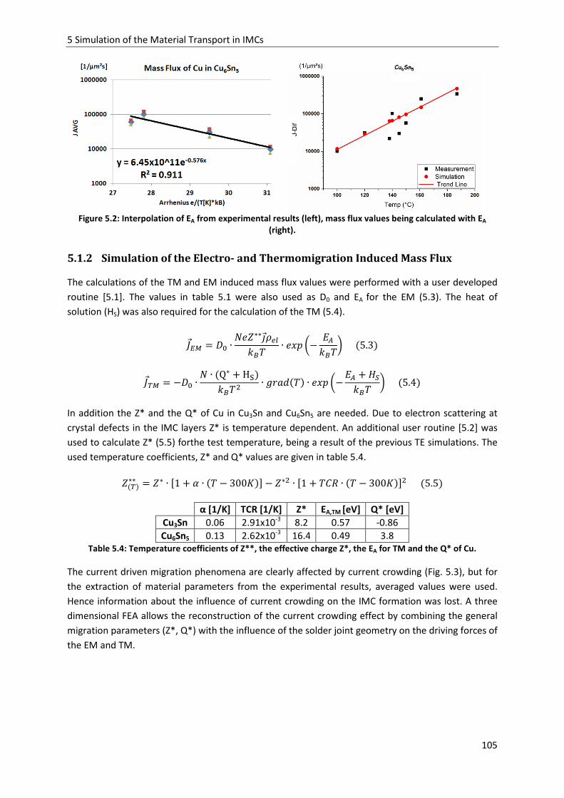
5 Simulation of the Material Transport in IMCs
105
Figure 5.2: Interpolation of EA from experimental results (left), mass flux values being calculated with EA
(right).
5.1.2 Simulation of the Electro- and Thermomigration Induced Mass Flux
The calculations of the TM and EM induced mass flux values were performed with a user developed
routine [5.1]. The values in table 5.1 were also used as D0 and EA for the EM (5.3). The heat of
solution (HS) was also required for the calculation of the TM (5.4).
lU- 6 ∙ o∗∗fGqKLM ∙ I <JKLMN 5.3
l- 6 ∙ ∙ Q∗ & H· KLM ∙ "Rt$M ∙ I<J &[KLM N5.4 In addition the Z* and the Q* of Cu in Cu3Sn and Cu6Sn5 are needed. Due to electron scattering at
crystal defects in the IMC layers Z* is temperature dependent. An additional user routine [5.2] was
used to calculate Z* (5.5) forthe test temperature, being a result of the previous TE simulations. The
used temperature coefficients, Z* and Q* values are given in table 5.4.
o ∗∗ o∗ ∙ 1 & ∙ M 300W o∗ ∙ 1 & M!s ∙ M 300W 5.5 α [1/K] TCR [1/K] Z* EA,TM [eV] Q* [eV]
Cu3Sn 0.06 2.91x10⁻³ 8.2 0.57 -0.86
Cu6Sn5 0.13 2.62x10⁻³ 16.4 0.49 3.8 Table 5.4: Temperature coefficients of Z**, the effective charge Z*, the EA for TM and the Q* of Cu.
The current driven migration phenomena are clearly affected by current crowding (Fig. 5.3), but for
the extraction of material parameters from the experimental results, averaged values were used.
Hence information about the influence of current crowding on the IMC formation was lost. A three
dimensional FEA allows the reconstruction of the current crowding effect by combining the general
migration parameters (Z*, Q*) with the influence of the solder joint geometry on the driving forces of
the EM and TM.
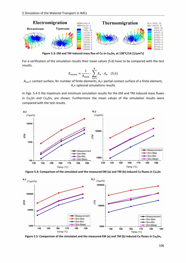
5 Simulation of the Material Transport in IMCs
106
Figure 5.3: EM and TM induced mass flux of Cu in Cu6Sn5 at 138°C/1A [1/µm²s]
For a verification of the simulation results their mean values (5.6) have to be compared with the test
results.
êYGEh 1)Y ∙ êh ∙ )h
m
h5.6
ASum= contact surface, N= number of finite elements, An= partial contact surface of a finite element,
Xn= optional simulations results
In Figs. 5.4-5 the maximum and minimum simulation results for the EM and TM induced mass fluxes
in Cu3Sn and Cu6Sn5 are shown. Furthermore the mean values of the simulation results were
compared with the test results.
Figure 5.4: Comparison of the simulated and the measured EM (a) and TM (b) induced Cu fluxes in Cu3Sn
Figure 5.5: Comparison of the simulated and the measured EM (a) and TM (b) induced Cu fluxes in Cu6Sn5
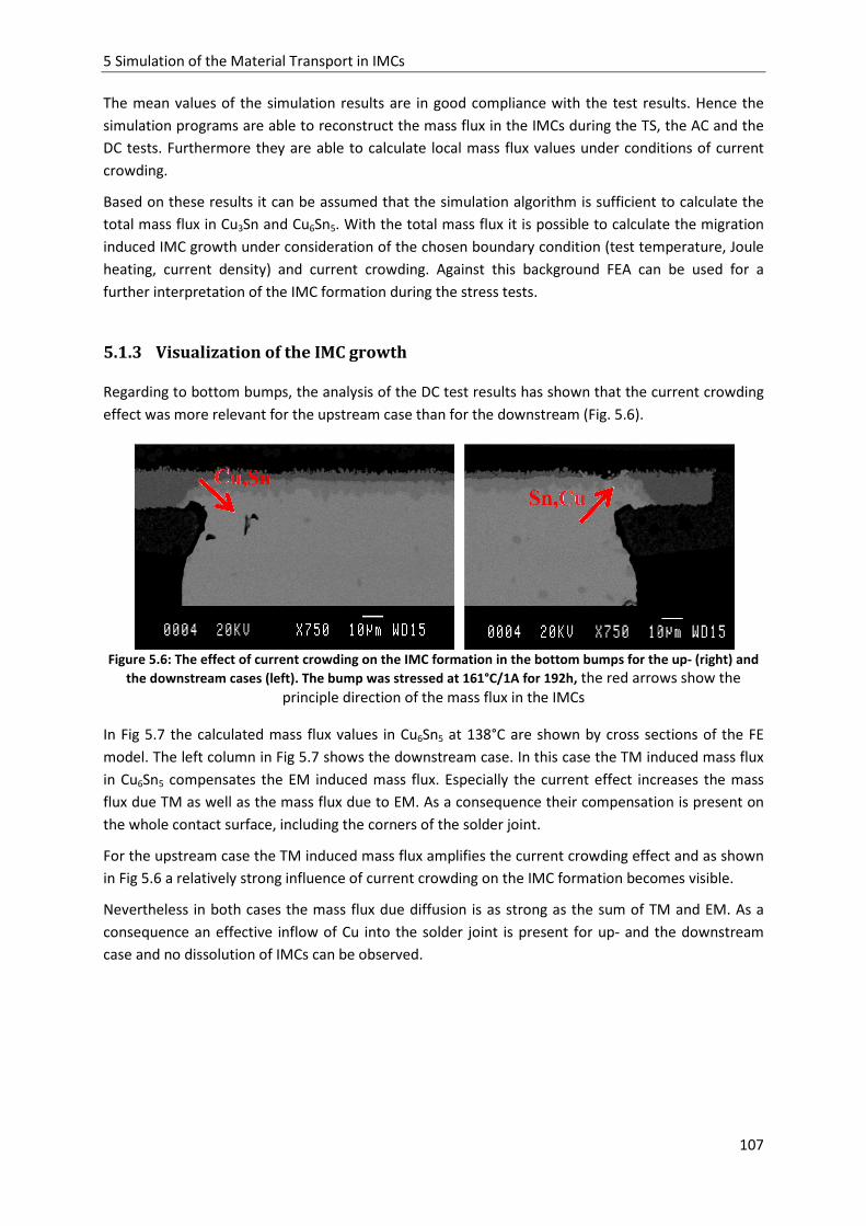
5 Simulation of the Material Transport in IMCs
107
The mean values of the simulation results are in good compliance with the test results. Hence the
simulation programs are able to reconstruct the mass flux in the IMCs during the TS, the AC and the
DC tests. Furthermore they are able to calculate local mass flux values under conditions of current
crowding.
Based on these results it can be assumed that the simulation algorithm is sufficient to calculate the
total mass flux in Cu3Sn and Cu6Sn5. With the total mass flux it is possible to calculate the migration
induced IMC growth under consideration of the chosen boundary condition (test temperature, Joule
heating, current density) and current crowding. Against this background FEA can be used for a
further interpretation of the IMC formation during the stress tests.
5.1.3 Visualization of the IMC growth Regarding to bottom bumps, the analysis of the DC test results has shown that the current crowding
effect was more relevant for the upstream case than for the downstream (Fig. 5.6).
Figure 5.6: The effect of current crowding on the IMC formation in the bottom bumps for the up- (right) and
the downstream cases (left). The bump was stressed at 161°C/1A for 192h, the red arrows show the
principle direction of the mass flux in the IMCs
In Fig 5.7 the calculated mass flux values in Cu6Sn5 at 138°C are shown by cross sections of the FE
model. The left column in Fig 5.7 shows the downstream case. In this case the TM induced mass flux
in Cu6Sn5 compensates the EM induced mass flux. Especially the current effect increases the mass
flux due TM as well as the mass flux due to EM. As a consequence their compensation is present on
the whole contact surface, including the corners of the solder joint.
For the upstream case the TM induced mass flux amplifies the current crowding effect and as shown
in Fig 5.6 a relatively strong influence of current crowding on the IMC formation becomes visible.
Nevertheless in both cases the mass flux due diffusion is as strong as the sum of TM and EM. As a
consequence an effective inflow of Cu into the solder joint is present for up- and the downstream
case and no dissolution of IMCs can be observed.

5 Simulation of the Material Transport in IMCs
108
Figure 5.7: The EM (“J-EM”), TM (“J-TM”), and diffusion induced (J-Dif) mass fluxes of Cu in Cu6Sn5, the total
mass flux (“J-Sum”) of Cu [1/µm²s]
With the total mass flux of Cu it is possible to calculate the momentary growth speed of Cu3Sn and
Cu6Sn5 (5.7-8).
e.2h l.,.2h ∙ 3.,. .,.h53.,. .,.2h5 ∙ 3.,.2h .,.h5 5.7
e.h l.,.h ∙ 3.,.2h .,hJÓ.53.,.2h .,.h5 ∙ 3.,.h .,hJÓ.55.8
For the dynamic simulation of the IMC formation during the stress tests, the test time was divided
into 100 time steps. For every time step the IMC growth speed was calculated and the IMC layer
thickness was increased by the product of the momentary IMC growth speed and the duration of the
time step (for more details see section 3.5.3).
The IMC dimensions at the starting point and at the end of the test time are shown in Fig. 5.8. As for
the experimental results a relatively thick and homogenous IMC layer was formed during the
downstream tests, and a relatively thin IMC layer with a clear current crowding profile was formed
during the upstream tests.
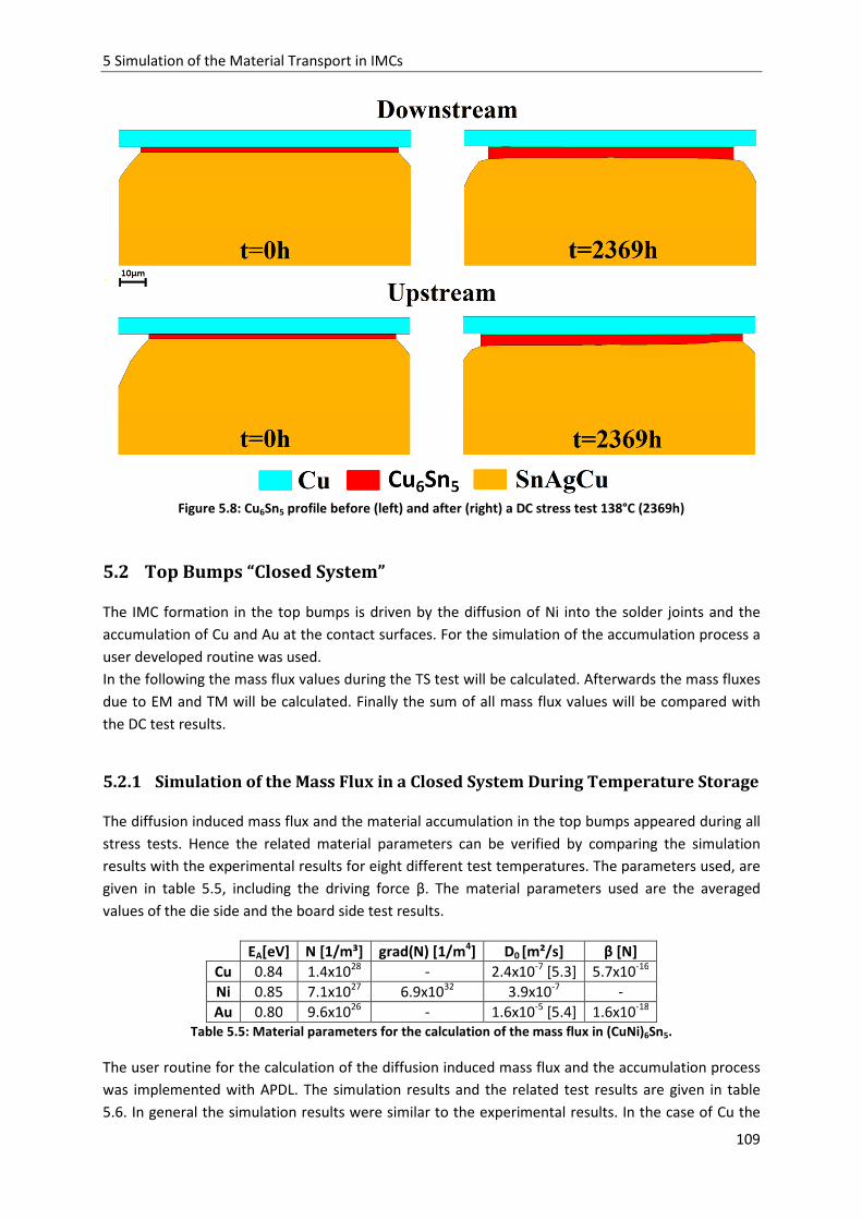
5 Simulation of the Material Transport in IMCs
109
Figure 5.8: Cu6Sn5 profile before (left) and after (right) a DC stress test 138°C (2369h)
5.2 Top Bumps “Closed System” The IMC formation in the top bumps is driven by the diffusion of Ni into the solder joints and the
accumulation of Cu and Au at the contact surfaces. For the simulation of the accumulation process a
user developed routine was used.
In the following the mass flux values during the TS test will be calculated. Afterwards the mass fluxes
due to EM and TM will be calculated. Finally the sum of all mass flux values will be compared with
the DC test results.
5.2.1 Simulation of the Mass Flux in a Closed System During Temperature Storage The diffusion induced mass flux and the material accumulation in the top bumps appeared during all
stress tests. Hence the related material parameters can be verified by comparing the simulation
results with the experimental results for eight different test temperatures. The parameters used, are
given in table 5.5, including the driving force β. The material parameters used are the averaged
values of the die side and the board side test results.
EA[eV] N [1/m³] grad(N) [1/m4] D0 [m²/s] β [N]
Cu 0.84 1.4x1028 - 2.4x10⁻⁷ [5.3] 5.7x10⁻¹⁶
Ni 0.85 7.1x1027 6.9x1032 3.9x10⁻⁷ -
Au 0.80 9.6x1026 - 1.6x10⁻⁵ [5.4] 1.6x10⁻¹⁸ Table 5.5: Material parameters for the calculation of the mass flux in (CuNi)6Sn5.
The user routine for the calculation of the diffusion induced mass flux and the accumulation process
was implemented with APDL. The simulation results and the related test results are given in table
5.6. In general the simulation results were similar to the experimental results. In the case of Cu the
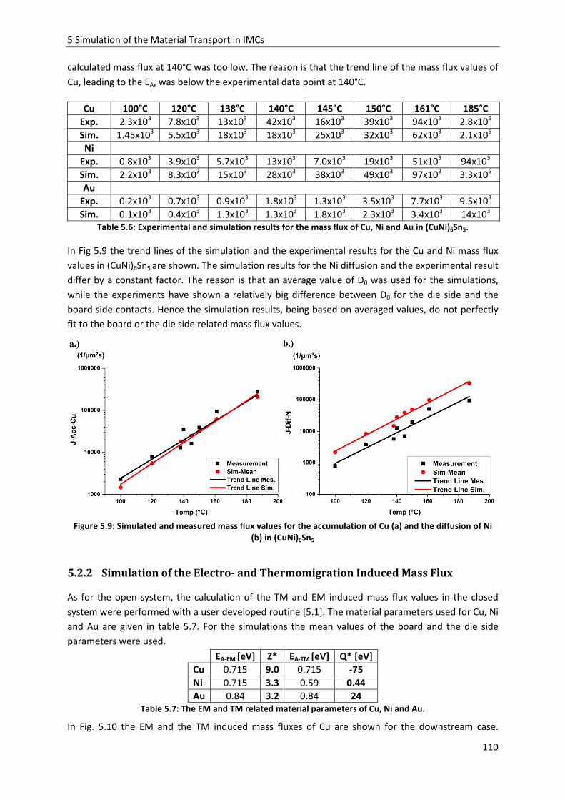
5 Simulation of the Material Transport in IMCs
110
calculated mass flux at 140°C was too low. The reason is that the trend line of the mass flux values of
Cu, leading to the EA, was below the experimental data point at 140°C.
Cu 100°C 120°C 138°C 140°C 145°C 150°C 161°C 185°C
Exp. 2.3x10³ 7.8x10³ 13x103 42x103 16x103 39x103 94x103 2.8x10⁵
Sim. 1.45x10³ 5.5x10³ 18x103 18x103 25x103 32x103 62x103 2.1x10⁵
Ni
Exp. 0.8x10³ 3.9x10³ 5.7x10³ 13x103 7.0x10³ 19x103 51x103 94x103
Sim. 2.2x10³ 8.3x10³ 15x103 28x103 38x103 49x103 97x103 3.3x10⁵
Au
Exp. 0.2x10³ 0.7x10³ 0.9x10³ 1.8x10³ 1.3x10³ 3.5x10³ 7.7x10³ 9.5x10³
Sim. 0.1x10³ 0.4x10³ 1.3x10³ 1.3x10³ 1.8x10³ 2.3x10³ 3.4x10³ 14x103 Table 5.6: Experimental and simulation results for the mass flux of Cu, Ni and Au in (CuNi)6Sn5.
In Fig 5.9 the trend lines of the simulation and the experimental results for the Cu and Ni mass flux
values in (CuNi)6Sn5 are shown. The simulation results for the Ni diffusion and the experimental result
differ by a constant factor. The reason is that an average value of D0 was used for the simulations,
while the experiments have shown a relatively big difference between D0 for the die side and the
board side contacts. Hence the simulation results, being based on averaged values, do not perfectly
fit to the board or the die side related mass flux values.
Figure 5.9: Simulated and measured mass flux values for the accumulation of Cu (a) and the diffusion of Ni
(b) in (CuNi)6Sn5
5.2.2 Simulation of the Electro- and Thermomigration Induced Mass Flux
As for the open system, the calculation of the TM and EM induced mass flux values in the closed
system were performed with a user developed routine [5.1]. The material parameters used for Cu, Ni
and Au are given in table 5.7. For the simulations the mean values of the board and the die side
parameters were used.
EA-EM [eV] Z* EA-TM [eV] Q* [eV]
Cu 0.715 9.0 0.715 -75
Ni 0.715 3.3 0.59 0.44
Au 0.84 3.2 0.84 24
Table 5.7: The EM and TM related material parameters of Cu, Ni and Au.
In Fig. 5.10 the EM and the TM induced mass fluxes of Cu are shown for the downstream case.

5 Simulation of the Material Transport in IMCs
111
Furthermore the accumulation was taken into account. The TM and the EM are strongly affected by
current crowding and the related mass fluxes densities are higher than the mass flux densities due to
material accumulation. This is a clear difference to the bottom bumps, because the related mass flux
values due to diffusion were as high as the sum of TM and EM.
Figure 5.10: The EM (left), TM (middle) induced mass fluxes and the accumulation (right) of Cu at the die and
the board side contact surfaces of a downstream stressed top bumps (138°C, 1A) [1/µm²s]
As shown in Fig. 5.11, the strong influence of EM can lead to a dissolution of the (CuNi)6Sn5 layer. The
dissolution of (CuNi)6Sn5 appeared at the die side contacts during the downstream tests. For the
upstream case a similar, but weaker, dissolution effect of (CuNi)6Sn5 was observed at the board side
contacts.
The formation of (CuNi)6Sn5 mainly depends on the Cu mass flux. The simulation results of the total
mass flux show that the reason for the dissolution of (CuNi)6Sn5 was the disappearance of Cu due the
EM induced mass flux. The TM and EM have opposite directions. Hence they should compensate
each other, but the current crowding led to smaller temperature gradients. As a consequence a
reduced mass flux due to TM was observed. The increased Joule heating due to current crowding
locally warmed up the relatively cold top bumps. Consequently the temperature of the affected
regions was closer to the maximum package temperature in the package and the temperature
gradients and the related mass flux due to TM become smaller. Under these conditions the EM
induced mass flux was not compensated by TM. In addition the EM induced mass flux was stronger
than the mass flux due to material accumulation.
At the board side contacts the TM and EM induced mass fluxes were able to compensate each other
and the IMC growth profile was relatively uniform.

5 Simulation of the Material Transport in IMCs
112
Figure 5.11: IMC dissolution after downstream DC stress (left) [5.5] and the sum of all Cu mass flux values
(right). [1/µm²s]
In addition to the migration of Cu, the EM and TM induced mass fluxes of Au and Ni were calculated.
The mass fluxes of Au and Ni did not have an influence on the (CuNi)6Sn5 formation speed, and the
Ni3Sn4 formation, as a consequence of EM driven Ni motion, was independent of the direction of the
current flow. Nevertheless the validation of the Z* and Q* values of Cu and Ni was possible by
comparing the mean value of the simulation results with the experimental results (Fig. 5.12-13).
In the main the calculated mass flux values due to EM fit to the experimental results. Only the mass
flux of Cu at 138°C was overestimated, because the simulation program does not take into account
the strong saturation effect on the Cu accumulation during the long term TS tests. The simulated and
the measured mass flux values due TM are similar in all cases.
Figure 5.12: Comparison of the simulated and the measured EM induced mass flux values of Cu, Ni and Au in
the top bumps [1/µm²s]
Figure 5.13: Comparison of the simulated and the measured TM induced mass flux values of Cu, Ni and Au in
the top bumps [1/µm²s]
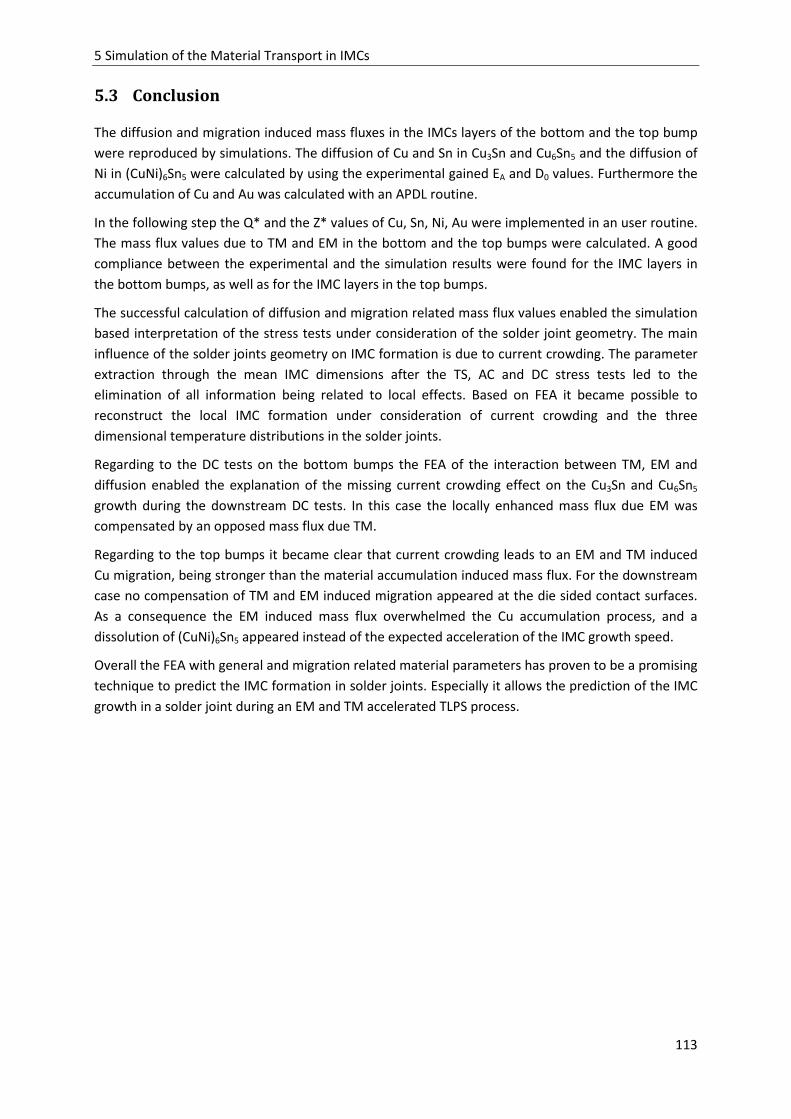
5 Simulation of the Material Transport in IMCs
113
5.3 Conclusion The diffusion and migration induced mass fluxes in the IMCs layers of the bottom and the top bump
were reproduced by simulations. The diffusion of Cu and Sn in Cu3Sn and Cu6Sn5 and the diffusion of
Ni in (CuNi)6Sn5 were calculated by using the experimental gained EA and D0 values. Furthermore the
accumulation of Cu and Au was calculated with an APDL routine.
In the following step the Q* and the Z* values of Cu, Sn, Ni, Au were implemented in an user routine.
The mass flux values due to TM and EM in the bottom and the top bumps were calculated. A good
compliance between the experimental and the simulation results were found for the IMC layers in
the bottom bumps, as well as for the IMC layers in the top bumps.
The successful calculation of diffusion and migration related mass flux values enabled the simulation
based interpretation of the stress tests under consideration of the solder joint geometry. The main
influence of the solder joints geometry on IMC formation is due to current crowding. The parameter
extraction through the mean IMC dimensions after the TS, AC and DC stress tests led to the
elimination of all information being related to local effects. Based on FEA it became possible to
reconstruct the local IMC formation under consideration of current crowding and the three
dimensional temperature distributions in the solder joints.
Regarding to the DC tests on the bottom bumps the FEA of the interaction between TM, EM and
diffusion enabled the explanation of the missing current crowding effect on the Cu3Sn and Cu6Sn5
growth during the downstream DC tests. In this case the locally enhanced mass flux due EM was
compensated by an opposed mass flux due TM.
Regarding to the top bumps it became clear that current crowding leads to an EM and TM induced
Cu migration, being stronger than the material accumulation induced mass flux. For the downstream
case no compensation of TM and EM induced migration appeared at the die sided contact surfaces.
As a consequence the EM induced mass flux overwhelmed the Cu accumulation process, and a
dissolution of (CuNi)6Sn5 appeared instead of the expected acceleration of the IMC growth speed.
Overall the FEA with general and migration related material parameters has proven to be a promising
technique to predict the IMC formation in solder joints. Especially it allows the prediction of the IMC
growth in a solder joint during an EM and TM accelerated TLPS process.

6 Conclusion & Perspectives
114
6 Conclusion & Perspectives

6 Conclusion & Perspectives
115
6.1 Conclusion
In this work the material motion, leading to the IMC formation during stress tests on SnAgCu solder
joints, was characterized with temperature storage (TS) tests that were partially combined with an
additional DC or AC load. The IMC growth during the TS tests appeared due to diffusion. If a current
was applied to the test structure also mass fluxes due to electro- (EM) and thermomigration (TM)
appeared.
All stress test were performed in ovens at a minimum temperature of 100°C. Hence the investigation
of the EM or TM related IMC formation, and the extraction of related material parameters was only
possible after the diffusion induced mass fluxes in the solder bumps were determined. Against this
background short term and long term TS tests were performed at 150°C. Afterwards the short term
tests were repeated at 100°C, 120°C and 140°C.
In case of the bottom bumps the diffusion of Cu from the metal line into the solder joints led to the
formation Cu3Sn and Cu6Sn5. During the long term tests the formation speed of both IMCs was
reduced with increasing layer thickness. Shrinking concentration gradients and a longer distance for
Cu to pass were identified as possible reasons for the long term effect. Being aware of possible long
term saturation affects, the TS tests at 150°C and the three additional TS tests could be used to
characterize the diffusion of Cu and Sn in Cu3Sn and Cu6Sn5. As results the activation energies (EA)
and the diffusion constants (D0) of Cu and Sn were extracted for both IMCs. The results were
compared with literature values. By that way the mathematical model for the mass flux extraction
could be validated and a six jump cycle, firstly described by Huntington, could be identified as the
most relevant transport mechanism for the motion of Sn and Cu in the investigated Cu3Sn and Cu6Sn5
layers.
In case of the top bumps the Ni pads acted as diffusion barrier for the motion of Cu coming from the
metal lines. Nevertheless during the TS tests a (CuNi)6Sn5 layer was formed by the accumulation of
Cu and the diffusion of Ni form the pads into the solder joints. As shown by previous experiments no
Ni3Sn4 formation was observable after the TS tests on Cu containing solder joints. The Cu source for
the (CuNi)6Sn5 formation was the 0.5% Cu content in SnAgCu. As a consequence the Cu content in the
solder was reduced during (CuNi)6Sn5 formation and a clear declaration of the (CuNi)6Sn5 formation
was observed during the long term TS tests. Taking into account the long term effects on the
(CuNi)6Sn5 formation, it was possible to characterize the diffusion of Ni and the accumulation of Cu by
extracting the mass flux values for four different storage temperatures. Like for the bottom bumps,
the EA for the motion Cu and Ni was determined. Before this step no literature values for the motion
of single elements in (CuNi)6Sn5 were available. For a more general description of the accumulation
related migration process the Nernst-Einstein equation was used to define a driving force “β”, being
responsible for the directed motion of the Cu atoms to contact surfaces. In difference to the Ni
diffusion the driving force β and the D0 of the Cu accumulation are part of one equation and only one
parameter could be extracted. Hence the D0 of Cu was taken from literature and β was calculated
from the mass flux values.
AC (0.8A/50Hz) stress tests at 145°C led to Joule heating and TM, but they also suppressed an
effective mass flux due to EM. The tests did not show any EM induced void formation in the solder
joints. Nevertheless the IMC formation in the top and in the bottom bumps was accelerated. The IMC
formation speed was independent from the direction of the current flow. Hence the presence of a

6 Conclusion & Perspectives
116
TM induced mass flux can be expected. At the contact surfaces of the top bumps no Ni3Sn4 was
found. Hence it became clear that a directed mass flux due to EM is needed to increase the Ni
portion in IMCs above the critical value for the Ni3Sn4 formation.
Taking into account that the applied current increases the test temperature, the expected mass flux
due diffusion was extrapolated with the EA and D0 values from the TS tests. Afterwards an extraction
of the TM induced mass flux in the top and bottom bumps was possible. Based on the TM induced
mass flux values the heat of transport (Q*) values for the TM induced motion of Cu and Sn in Cu3Sn
and Cu6Sn5 as well as for the Cu, Ni motion in (CuNi)6Sn5 could be determined.
Unlike the TS and TM tests, the DC tests led to the formation of a Ni3Sn4 IMC layer at the contact
surfaces of the top bumps. The EM induced mass flux increased the Ni content in (CuNi)6Sn5. EDS
investigations have shown that an atomic concentration of 25% is the critical amount of Ni being
needed for the Ni3Sn4 formation. Like for the AC tests an accelerated IMC formation speed was
observable in the top and in the bottom bumps. The applied DC led to void formation in the solder
joints and the IMC formation speed was influenced by the direction of the current flow. Both effects
clearly indicate the presence of EM. A difference between the mean IMC dimensions at the board
and the die side contact surfaces also indicate the presence of a TM induced mass flux.
By comparing the IMC dimensions for upstream and the downstream case the EM induced mass flux
in bottom and in the top bumps could be extracted. After the extrapolation of the diffusion and
material accumulation related mass flux values also the TM induced mass flux was available. Based
on these additional results effective charge values (Z*) at three different temperatures and Q* values
for four different test temperatures were extracted. These values were used to describe the
temperature dependency of the EM and the TM induced mass fluxes in Cu3Sn, Cu6Sn5, (CuNi)6Sn5 and
Ni3Sn4.
The results of this analysis are temperature independent values of Z* and Q* for the calculation of
the EM and TM induced mass flux in the IMCs. Combined with the influence by diffusion and the
related parameters (EA, D0) they can be used for the prediction of the IMC growth speed in solder
joints for a broad range of boundary conditions.
For the interpretation of the experimental results and the extraction of the material parameters
averaged values were used. Hence localized effects like current crowding could not be investigated.
Based on the three dimensional FE model the test conditions could be reconstructed and the IMC
profile after the DC tests could be explained by taking into account the influence of current crowding
on the IMC formation speed.
In case of the bottom bumps the EM and the TM induced mass fluxes compensate each other for the
downstream case and were added for the upstream case. The sum of the mass fluxes due to TM and
EM was as big as the mass flux due to diffusion. Hence the interaction between the three mass flux
values could explain why the IMC profile was relatively homogenous for the downstream case, while
the influence of current crowding became clearly visible for the upstream case.
Regarding to the top bumps the mass flux values due to TM and EM were added for the downstream
case and they compensated each for the upstream case. In difference to the bottom bumps the TM
and EM induced mass fluxes were stronger than the mass flux due material accumulation. Hence the
simulations could show why the downstream case shows a complete dissolution of the (CuNi)6Sn5
layer.

6 Conclusion & Perspectives
117
6.2 Perspectives
Based on this work it is possible to predict the IMC formation speed in SnAgCu solder joints for a
wide variation of process temperatures under consideration of EM and TM induced mass fluxes. A
prediction of the IMC formation, being based on temperature independent material values, enables
the simulation based optimization of the TLPS process parameters and the solder joint geometry. The
availability of temperature independent Z* and Q* also enables the development and the
optimization of EM and TM accelerated TLPS. EM and TM enhanced TLPS could enable the reduction
of the process temperature or the application of TLPS on Sn layers being normally too thick to
transform into an IMC joint in a reasonable time. This can be done for direct metal to solder contacts
as well as for solder joints on Ni/Au contact pads.
The experimental approach of this work and the related model for the IMC formation describe a
general method for the characterization of the IMC formation due to EM and TM. Hence an EM and
TM accelerated TLPS could also be developed for alternatives to SnCu IMCs, like AuSn or Au5Sn.
In addition the prediction of the IMC formation with respect to the influences by EM and TM
supports the development of simulation tools for the investigation of aging effects on conventional
SnAgCu solder joints.
References
118
References
Chapter 2:
[2.1] E.M Rogers, "Diffusion of Innovations 5th Edition", Free Press, New York, 2003, pp. 234, 281.
[2.2] S. Ram, J. N. Sheth, "Consumer Resistance to Innovations: The Marketing Problem and its
Solutions ", The Journal of Consumer Marketing, Vol.6 No.2 (1989), pp. 5-13.
[2.3] J. N. Sheth, S. Ram, "Bringing innovation to market: how to break corporate and customer
barriers", Wiley, New Jersey, 1987, pp.3-4, 64.
[2.4] S . Ram, J. N. Sheth, " Marketing Barriers to Innovations: The case of the Entrepreneur", AMA
Symposium on Research Activities in Marketing Entrepreneurship, 1988, pp. 403-409.
[2.5] G. E. Moore, “Cramming more Components onto Integrated Circuits,” Electronics, Vol. 38
No. 8 (1965), reproduced in IEEE Proceedings Vol. 86 No. 1 (1998) pp. 82-85.
[2.6] R. H. Dennard, F. H. Gänßlen, H. N. Yu et al., “Design of ion-implanted MOSFETs with very
small physical dimensions”, IEEE, Journal of Solid-State Circuits, Vol. 9 (1974), p.256 -268.
[2.7] M. Kawano, S. Uchiyama, Y. Egawa et al. "A 3D Packaging Technology for 4 Gbit Stacked
DRAM with 3 Gbps Data Transfer", IEEE, International Electron Devices Meeting (IEDM), San
Francisco, December 2006, pp. 1-3.
[2.8] Raymond A. Fournelle, „Lead-Free Solders and Processing Issues in Microelectronics“, JOM,
2003, pp. 49.
[2.9] G. Philip, "Wafer Level Chip Scale Packaging (WL-CSP): An Overview", IEEE, Transactions
Advanced Packaging, Vol. 23, No. 2, MAY 2000, pp. 198-205.
[2.10] Y. Nishi, R. Doering, "Handbook of Semiconductor Manufacturing Technology ", 2nd Edition,
CRC Press, Boca Raton, Florida, 2007, chapter 4, 11, 30, 35.
[2.11] C. Auth, C. Allen, A. Blattner et al., " A 22nm High Performance and Low-Power CMOS
Technology Featuring Fully-Depleted Tri-Gate Transistors, Self-Aligned Contacts and High
Density MIM Capacitors ", IEEE, Symposium on VLSI Technology Digest of Technical Papers,
Honulu, Hawai, 2012, pp. 131-132.
[2.12] C.-H. Jan, U. Bhattacharya, R. Brain et al., "A 22nm SoC Platform Technology Featuring 3-D
Tri-Gate and High-k/Metal Gate, Optimized for Ultra Low Power, High Performance and High
Density SoC Applications", IEEE, International Electron Devices Meeting (IEDM), San
Francisco, December 2012, pp. 44-47.
[2.13] R. H. Havemann, J. A. Hutchby, "High-Performance Interconnects: An Integration Overview",
IEEE Proceedings Vol. 86 No. 5 (2001) pp. 586-601.
[2.14] S. Borkar, "Design challenges of technology scaling", IEEE, Micro, Vol. 14 No. 4 (1999), pp. 23-
29.
[2.15] S. E. Thompson, S. Parthasarathy, "Moore's law: the future of Si microelctronics", materials
today, Vol. 9 No. 6 (2006), pp. 20-25.
[2.16] G. Messner, "Cost-Density Analysis of Interconnections", IEEE, Components, Hybrids, and
Manufacturing Technology, Vol. 10 No. 2 (1987), pp. 143-151.

References
119
[2.17] K. Rupp, S. Selberherr, "The Economic Limit to Moore’s Law", IEEE, Transactions on
Semiconducter Manufactoring, Vol. 24, No. 1 (2011), pp. 1-3.
[2.18] International Monetary Fund, "World Ecomoic Outlook Update", Wshignton D.C., USA, 2012,
pp. 1-8.
[2.19] R. K. Cavin, P. Lugli, V. V. Zhirnov, "Science and Engineering Beyond Moore’s Law", IEEE
Proceedings Vol. 100 (2012) pp. 1720-1749.
[2.20] Semiconductor Industry Association, The International Technology Roadmap for
Semiconductors, 2009.
[2.21] W. Arden, M. Brillouët, P. Cogez, et al. "Towards a Moore Than Moore Roadmap", CATRENE©
Scientific Committee, 2011.
[2.22] R. W. Johnson, J. L. Evans, P. Jacobsen, The Changing Automotive Environment: High-
Temperature Electronics, IEEE, Transactions Electronics Packaging Manufacturing, Vol. 27 No.
3 (2004), pp. 164-176.
[2.23] M. L. ElGizawy, "Continuous Measurement-While-Drilling Surveying System Utilizing MEMS
Inertial Sensors", Dissertation, University of Calgary, Department of Geomatics Engineering,
Calgary, Alberta, 2009.
[2.24] F. G. Kuper, "Automotive IC reliability: Elements of the battle towards zero defects", “, IEEE,
Microelectronics Reliability, Vol. 48 (2008), pp. 1459-1463.
[2.25] R. Kisiel, Z. Szczepański, „Trends in assembling of advanced IC packages“, Journal of
Telecommunication and Information technology, 2005, pp. 63-69.
[2.26] R. R. Tummala, E. J. Rymaszewski, A. G. Klopfenstein, “Microelectronics Packaging
Handbook”, 2nd Edition, Springer Science and Business Media, Berlin, Germany, 1997, pp.
65, 84, 470, 476.
[2.27] K. DeHaven, J. Dietz, „Controlled Collapse Chip Connection (C4) - An Enabling Technology“,
IEEE, Electronic Components and Technology Conference (ECTC), Washington D.C. , June
1994, pp. 1-6.
[2.28] Semiconductor Industry Association, The International Technology Roadmap for
Semiconductors 2010 Update, 2010.
[2.29] P. Ramm, J. J. Q. Lu, M. M. V. Taklo, "Handbook of Waferbonding", Wiley-VCH Verlag,
Weinheim, Germany, 2012, pp. 162-167, 181-185, 204-209, 305.
[2.30] J. Cheng Lin, J. Yu, B. Chung et. al : “Development on Ultra High Density Memory Package
with PoP Structure “, IEEE, Electronic Components and Technology Conference (ECTC) 2011,
Orlando, pp. 1136-1140.
[2.31] L. Meinshausen, K. Weide-Zaage, H. Frémont, „Thermal Management for Stackable Packages
with Stacked ICs", IEEE, Mechanical & Multi-Physics Simulation, and Experiments in
Microelectronics and Microsystems (EuroSimE), Lisbon, 2012, pp. 1-6.
[2.32] H. Gan, S.L. Wright, R. Polastre, et al., "Pb-free Micro-joints (50 μm pitch) for the Next
Generation Micro-systems: the Fabrication, Assembly and Characterization", IEEE, Electronic
Components and Technology Conference (ECTC), 2006, Marina, California, pp. 1210-1215.

References
120
[2.33] S. Gee, N. Kelkar, J. Huang, “Lead-Free and PbSn Bump Electromigration Testing”, ASME
International Technical Conference and Exhibition on Packaging and Integration of Electronic
and Photonic Microsystems (InterPACK), 2005, San Francisco, pp. 1-9.
[2.34] B. Salam, N. N. Ekere, D. Rajkumar, "Study of the Interface Microstructure of Sn-Ag-Cu Lead-
Free Solders and the Effect of Solder Volume on Intermetallic Layer Formation", IEEE,
Electronic Components and Technology Conference (ECTC), 2001, Orlando, Florida, pp. 1-7.
[2.35] L. Meinshausen, H. Frémont, K. Weide-Zaage, „Migration induced IMC formation in SAC305
solder joints on Cu, NiAu and NiP metal layers“, IEEE, Microelectronics Reliability, Vol. 52 No
9-10 (2012), pp. 1827-1832.
[2.36] Semiconductor Industry Association, The International Technology Roadmap for
Semiconductors, 2002.
[2.37] Semiconductor Industry Association, The International Technology Roadmap for
Semiconductors 2012 Update, 2012.
[2.38] M. Abtewa, G. Selvaduray, "Lead-free Solders in Microelectronics", Materials Science and
Engineering, Vol. 27 (2000), pp. 95-141.
[2.39] P. G. Shewmon, "Diffusion in Solids", 2nd Edition, Wiley, New York City, 1989, pp. 37, 54-74.
[2.40] J. Philibert, “Creep and Diffusion”, Solid State Ionics, Vol. 12 (1984), pp. 321-336.
[2.41] M.D. Mathew, H. Yang, S. Movva, „Creep Deformation Characteristics of Tin and Tin-Based
Electronic Solder Alloys“, Metallurgical and Materials Transactions A, Vol. 36A (2005), pp. 99-
105.
[2.42] M. R. Werner, „Review on materials, microsensors, systems and devices for high-
temperature and harsh-environment applications“, IEEE, Industrial Electronics, Vol. 48 No. 2
(2001), pp. 249-257.
[2.43] R. Klieber, „Evaluation of materials for high temperature IC packaging“, 15th International
Workshop on Thermal Investigations of ICs and Systems (THERMINIC), Leuven, Belgium,
2009, pp. 117-120.
[2.44] R. G. Azevedo, „A SiC MEMS Resonant Strain Sensor for Harsh Environment Applications“,
IEEE, Sensors Journal, Vol. 7 No. 4 (2007), pp. 568-576.
[2.45] K. N. Chen, „Microstructure examination of copper wafer bonding“, Journal of Electronic
Materials, Vol. 30 No. 4 (2001), pp. 331-335.
[2.46] T. H. Kim, M. M. R. Howlader, T. Itoh, et al. "Room temperature Cu–Cu direct bonding using
surface activated bonding method", Journal of Vacuum Science & Technology A: Vacuum,
Surfaces, and Films, Vol. 21 No. 2, p. 449-453.
[2.47] P. Gueguen, L. Di Cioccio, P. Gergaud, "Copper Direct-Bonding Characterization and Its
Interests for 3D Integration", The Electrochemical Society, Vol. 16 No. 8 (2008), pp. 31-37.
[2.48] E. Ide, S. Angata, A. Hirose, "Metal–metal bonding process using Ag metallo-organic
nanoparticles", Acta Materialia, Vol. 53 (2005), pp. 2385–2393.
[2.49] G. Zou, J. Yan, F. Mu, "Low Temperature Bonding of Cu Metal through Sintering of Ag
Nanoparticles for High Temperature Electronic Application", The Open Surface Science
Journal, Vol. 3 (2011), pp. 70-75.

References
121
[2.50] A. Hu, J. Y. Guo, H. Alarifi, "Low temperature sintering of Ag nanoparticles for flexible
electronics packaging", Applied Physics Letters , Vol. 97 (2010), pp. 1-3.
[2.51] A. Moujbani, J. Kludt, K. Weide-Zaage, “Dynamic Simulation of Migration Induced Failure
Mechanism in Integrated Circuit Interconnects”, IEEE, Microelectronics Reliability, Vol. 53
(2013), pp. 1365-1369.
[2.52] N. Watanabe, T. Kojima, T. Asano, "Wafer-level Compliant Bump for Three-Dimensional LSI
with High-Density Area Bump Connections", International Electron Devices Meeting (IEDM),
Washington D. C., December 2005, pp. 671-673.
[2.53] I. Tuah-Poku, M. Dollar, T. B. Massalski, "A Study of the Transient Liquid Phase Bonding
Process Applied at Ag/Cu/Ag Sandwich Joint", Mtallurgical Transactions A, Vol. 19A (1988),
pp. 675-686.
[2.54] R. Agarwal, W. Zhang, P. Limaye, "Cu/Sn Microbumps Interconnect for 3D TSV Chip Stacking",
IEEE, Electronic Components and Technology Conference (ECTC), 2010, Las Vegas, pp. 858-
863.
[2.55] K. Guth, D. Siepe, J. Görlich, et al., „New assembly and interconnects beyond sintering
methods“, Power Conversion and Inteligent Motion (PCIM), Nürnberg, Germany, 2010, pp. 1-
6.
[2.56] K.S. Kim, S.H. Huh, K. Suganuma, "Effects of intermetallic compounds on properties of Sn–
Ag–Cu lead-free soldered joints", Journal of Alloys and Compounds, Vol. 352 (2003), pp. 226–
236.
[2.57] H. B. FAN, E. K. L. Chan, C. K.Y. Wong, "Moisture Diffusion Study in Electronic Packaging using
Molecular Dynamic Simulation", IEEE, Electronic Components and Technology Conference
(ECTC), 2006, Marina, California, pp. 1425-1428.
[2.58] M. Kitano, A. Nishimura, S. Kawai, et al. "Analysis of Package Cracking During Reflow
Soldering Process", IEEE, 26th International Reliability Physics Symposium, Monterey,
California, 1988, pp. 90-95.
[2.59] I.Fukuzawa, S.Ishiguro, S.Nanbu et al., "Moisture Resistance Degardation of Plastic LSIs by
Reflow Soldering", IEEE, 23rd International Reliability Physics Symposium, New York, 1985,
pp. 192-197.
[2.60] K. Weide-Zaage, W. Horaud, H. Frémont, "Moisture diffusion in Printed Circuit Boards :
Measurements and Finite- Element- Simulations", IEEE, Microelectronics Reliability, Vol. 45
(2005), pp. 1662-1667.
[2.61] JEDEC JESD22-A101C, “Steady State Temperature Humidity Bias Life Test”, March 2009.
[2.62] Kh. G. Schmitt-Thomas, S. Wege, H. Schweigart, "Elektrochemische Migration - eine typische
Korrosionserscheinung in der Mikroelektronik", Materials and Corrosion, Vol. 46 (1995), pp.
366-369, in German.
[2.63] E. H. Wong, K.C. Chan, R. Rajoo, "The Mechanics and Impact of Hygroscopic Swelling of
Polymeric Materials in Electronic Packaging", IEEE, Electronic Components and Technology
Conference (ECTC), 2000, Las Vegas, pp. 576-580.
References
122
[2.64] E. H. Wong, Y. C. Teo, T. B. Lim, " Moisture Diffusion and Vapour Pressure Modeling of IC
Packaging", IEEE, Electronic Components and Technology Conference (ECTC), 1998, Seattle,
USA, pp. 1372-1378.
[2.65] W. Feng, “Caractérisation Expérimentale et Simulation Physique des Mécanismes de
dégradation de Interconnexions sans plomb dans les technologies d’assemblage a très forte
densité d’intégration “”Boitier sur Boitier”, Dissertation, Université Bordeaux I, Talence,
France, 2010, in French.
[2.66] J. W. Yoon, B.-I. Noh, Y.-H. Lee, "Effects of isothermal aging and temperature–humidity
treatment of substrate on joint reliability of Sn–3.0Ag–0.5Cu/OSP-finished Cu CSP solder
joint", Microelectronics Reliability, Vol. 48 (2008), pp. 1864–1873.
[2.67] H. Huebner, S. Penka, B. Barchmann et al., „Microcontacts with sub-30 μm pitch for 3D chip-
on-chip integration, Microelectronic Engineering“, Microelectronic Engineering, Vol. 83 No.
11–12 (2006), pp. 2155-2162,
[2.68] P. J. Boddys, R. H. Delaney, J. N. Lahti, "Accelarated Life Testing of Flexible Printing Circuits",
14th Reliability Physics Symposium, Las Vegas, 1976, pp. 108-117.
[2.69] D. Q. Yu, W. Jillek , E. Schmitt, "Electrochemical migration of lead free solder joints", Journal
of Materials Science: Materials in Electronics, Vol. 17 (2006), pp. 229–241.
[2.70] K. M. Striny, A. W. Schelling, "Reliability Evaluation of Aluminum-Metallized MOS Dynamic
RAM's in Plastic Packages in High Humidity and Temperature Environments", IEEE,
Transactions on Components Hybrids and Manufactoring, Vol. 4 No. 4 (1981), pp. 476-481.
[2.71] M. S. Jung, S. B. Lee, H. Y. Lee, " Improvement of Electrochemical Migration Resistance by
Cu/Sn Inter-Metallic Compound Barrier on Cu in Printed Circuit Board ", IEEE, Transactions on
Device and Materials Reliability, Vol. 99 (2012), pp. 1-8.
[2.72] C. Xu, Y. Zhang, C. Fan, “Understanding Whisker Phenomenon – Driving Force for the Whisker
Formation”, IPC, Surface Mount Equipment Manufacturers Association, 2006, pp. 1-6.
[2.73] JEDEC JESD22-B112A, „Package Warpage Measurement of Surface-Mount Integrated Circuits
at Elevated Temperature“, October 2009.
[2.74] W.W. Lee, L.T. Nguyen, G.S. Selvaduray et al. „Solder joint fatigue models: review and
applicability to chip scale packages“, Microelectronics Reliability, Vol. 40 (2000), pp. 231–
243.
[2.75] JEDEC JESD22-A104D, „Temperature Cycling“, March 2009.
[2.76] S. S. Manson, “Fatique: A Complex Subject – Some Simple Approximations”, Experimental
Mechanics, 1964, pp. 193-226.
[2.77] S.B. Brown, K.H. Kim, L. Anand, “An internal variable constitutive model for hot working of
metals”, International Journal of Plasticity, vol. 5 (1989), pp. 95-130.
[2.78] M. Pei and J. Qu, “Constitutive modeling of lead-free solders,” ASME: Adv. Electron. Package,
pp. 1307–1311, 2005.
[2.79] Y. Liu, S. Irving, T. Luk et al., „3D Modeling of Electromigration Combined with Thermal-
Mechanical Effect for IC Device and Package “, Microelectronics Reliability, Vol. 48 (2008),
pp. 811–823.

References
123
[2.80] Y. L. Huang, K. L. Lin, „Microstructure evolution and micro impact performance of Sn–Ag–Cu
solder joints under thermal cycle test“, Journal of Materials Research, Vol. 25 No. 7, 2010, pp.
1312-1320.
[2.81] M. Meilunas, A. Primavera, O. Steven, „Reliability and Failure Analysis of Lead-Free Solder
Joints“, Proceedings of the IPC Annual Meeting, 2003, Minneapolis, USA, pp. 1-15.
[2.82] J. Y. Kim, J. Yu, „Effects of residual impurities in electroplated Cu on the Kirkendall void
formation during soldering“, Applied Physics Letters , Vol, 92 No. 9 (2008), pp. 1-3.
[2.83] L. Xu, J. H.L. Pang, F. Che, „Impact of Thermal Cycling on Sn-Ag-Cu Solder Joints and Board-
Level Drop Reliability“, Journal of Eelctronic Materials, Vol. 37, No. 6 (2008), pp. 880-886.
[2.84] J. Y. Lee, T. K. Hwang, J.Y. Kim: „Study on the Board Level Reliability Test of Package on
Package (PoP) with 2nd Level Underfill“, IEEE, Electronic Components and Technology
Conference (ECTC), 2007, pp.1905-1910.
[2.85] R. Labie, P. Limaye, K.W. Lee et al. “Reliability testing of Cu-Sn intermetallic micro-bump
interconnections for 3D-device stacking”, Electronic System-Integration Technology
Conference (ESTC), Berlin, 2010, pp. 1-5.
[2.86] Y. B. Kim, H. Noguchi, M. Amagai, „Vibration fatigue reliability of BGA-IC package with Pb-
free solder and Pb–Sn solder“, Microelectronics Reliability, Vol. 46 (2006), pp. 459–466.
[2.87] S. F. Wong, P. Malatkar, C. Rick et al., „Vibration Testing and Analysis of Ball Grid Array
Package Solder Joints“, IEEE, Electronic Components and Technology Conference (ECTC),
2007, Reno, Nevada, USA, pp. 373-380.
[2.88] T. Pringle, P. Raghavan, P. Malatkar, „Solder Joint Reliability of BGA Package under End-User
Handling Test Conditions“, IEEE, Electronic Components and Technology Conference (ECTC),
2007, Reno, Nevada, USA, pp. 400-406.
[2.89] E.H. Wong, K.M. Lim, N. Lee et al., „Drop Impact Test - Mechanics & Physics of Failure“, 4th
Electronics Packaging Technology Conference (EPTC), Singapore, 2002, pp. 327-333
[2.90] T.C. Chai, S. Quek, W. Y. Hnin et al., „Board Level Drop Test Reliability of IC Packages“, IEEE,
Electronic Components and Technology Conference (ECTC), 2005, Lake Buena Vista, Florida,
pp. 630-636.
[2.91] JEDEC JESD22-B111, „Board Level Drop Test Method of Components for Handheld Electronic
Products“, July 2003.
[2.92] J. M. Song, B. R. Huang, C. Y. Liu, „Nanomechanical responses of intermetallic phase at the
solder joint interface – Crystal orientation and metallurgical effects“, Materials Science and
Engineering, A 534 (2012), pp. 53– 59.
[2.93] J. M. Song, Y. L. Shen, C.-W. Su et al., „Strain Rate Dependence on Nanoindentation
Responses of Interfacial Intermetallic Compounds in Electronic Solder Joints with Cu and Ag
Substrates“, Materials Transactions, Vol. 50 No. 5 (2009), pp. 1231-1234.
[2.94] H. John , L. Pang, B. S: Xiong et al., „Modeling Stress Strain Curves For Lead-Free 95.5Sn-
3.8Ag-0.7Cu Solder“ ,IEEE, Mechanical & Multi-Physics Simulation, and Experiments in
Microelectronics and Microsystems (EuroSimE), Brussels, Belgium, 2004, pp. 449-453.

References
124
[2.95] C. C. Lee, P. J. Wang, J. S. Kim, „Are Intermetallics in Solder Joints Really Brittle?“, IEEE,
Electronic Components and Technology Conference (ECTC), 2007, Reno, Nevada, USA, pp.
648-652.
[2.96] S .K. W. Seah, C.T. Lim, E. H. Wong, „Mechanical Response of PCBs in Portable Electronic
Products During Drop Impact“, 4th Electronics Packaging Technology Conference (EPTC),
Singapore, 2002, pp. 120-125.
[2.97] T. Mattila, „ Reliability of High Density Lead-Free Solder Interconnections Under Thermal
Cycling and Mechanical Shock Loading”, Dissertation, Helsinki, Helsinki University of
Technology, Laboratory of Electronics Production Technology, 2005.
[2.98] X. Yanghua, L. Chuanyan, X. Xiaoming, “Effect of Interfacial Reactions on the Reliability of
Lead-Free Assemblies after Board Level Drop Tests”, Journal of Electronic Materials, Vol. 36
No. 9 (2007), pp. 1129-1136.
[2.99] D. Y.R. Chong , F.X. Che, J. H.L. Pang, „Drop impact reliability testing for lead-free and lead-
based soldered IC packages“, Microelectronics Reliability, Vol. 46 (2006), pp. 1160–1171.
[2.100] H. Wever, “Elektro und Thermotransport in Metallen”, Johann Ambrosius Barth, Lebzig, 1973,
in German, pp. 56, 232.
[2.101] C. Chen, H.M. Tong, K.N. Tu, “Electromigration and Thermomigration in Pb-Free Flip-Chip
Solder Joints”, Annual Review of Materials Research, Vol. 40 (2010), pp. 531-555.
[2.102] I. A. Blech, “Electromigration in thin aluminum films on titanium nitride“, Journal of Applied
Physics, Vol. 47 (1976), pp. 1203-1208.
[2.103] Y. Hou, C. M. Tan, „Blech Effect in Cu Interconnects with Oxide and Low-k Dielectrics“, 14th
International Symposium on the Physical and Failure Analysis of Integrated Circuits (IPFA),
2007, Bangalore, India, pp. 65-69.
[2.104] V.M. Dwyer, „Analysis of critical-length data from Electromigration failure studies“,
Microelectronics Reliability, Vol. 51 (2011), pp. 1568–1572.
[2.105] L. Meinshausen, K. Weide-Zaage, H. Frémont, “Electro- and Thermomigration induced Failure
Mechanisms in Package on Package“, IEEE, Microelectronics Reliability, Vol. 52 No 12 (2012),
pp. 2889-2906.
[2.106] JEDEC JEP154, “Guideline for Characterizing Solder Bump Electromigration under Constant
Current and Temperature Stress”, January 2008.
[2.107] J. R. Black, “Electromigration of Al-Si Alloy Films”, IEEE, 16th Annual International Reliability
Physics Symposium (IRPS), San Diego, California, 1978, pp. 233-236.
[2.108] K. Weide-Zaage, “Untersuchungen von Stromdichte-, Temperatur- und
Massenflussverteilungen in Viastrukturen integrierter Schaltungen”, Dissertation, VDI Verlag,
Düsseldorf, 1994, in German.
[2.109] C. Hau-Riege, R. Zang, Y. W. Yau, et al. „Electromigration Studies of Lead-Free Solder Balls
used for Wafer-Level Packaging“, IEEE, Electronic Components and Technology Conference
(ECTC), 2011, Lake Buena Vista, Florida, pp. 717-721.

References
125
[2.110] K. Nakagawa, S. Baba, M. Watanabe, et al. „Thermo-Electromigration Phenomenon of Solder
Bump, Leading to Flip-Chip devices with 5,000 Bumps“, IEEE, Electronic Components and
Technology Conference (ECTC), 2001, Orlando, Florida, pp. 1-7.
[2.111] K. Weide-Zaage, H. Frémont, L. Wang, “Simulation of migration effects in PoP“,IEEE,
Mechanical & Multi-Physics Simulation, and Experiments in Microelectronics and
Microsystems (EuroSimE), Freiburg, Germany, 2008, pp. 1-7.
[2.112] K. Weide-Zaage, “Simulation of Migration Effects in Solder Bumps”, IEEE, Transactions on
Device and Materials Reliability, Vol. 8 No. 3 (2008), pp. 442-448.
[2.113] L. Meinshausen, K. Weide-Zaage, M. Petzold, “Electro- and thermomigration in microbump
interconnects for 3D integration”, IEEE, Electronic Components and Technology Conference
(ECTC), 2011, Lake Buena Vista, Florida, pp. 1444-1451.
[2.114] L. Meinshausen, K. Weide-Zaage , H. Frémont, „Migration induced material transport in Cu-
Sn IMC and SnAgCu micro bumps“, IEEE, Microelectronics Reliability, Vol. 51 No 9-11, 2011,
pp. 1860-1863.
[2.115] B. H. L. Chao, X. Zhang, S. H. Chae, P. S. Ho, „Recent advances on kinetic analysis of
electromigration enhanced intermetallic growth and damage formation in Pb-free solder
joints“, IEEE, Microelectronics Reliability, Vol. 49 No. 9-11, 2009, pp. 253-263.
[2.116] B. Chao, S. H. Chae, Xuefeng Zhang, et al. „Electromigration enhanced intermetallic growth
and void formation in Pb-free solder joints“, Journal of Applied Physics, Vol. 100 (2006), pp.1-
10.
[2.117] S. H. Chae, B. Chao, X. Zhang, „ Investigation of Intermetallic Compound Growth Enhanced by
Electromigration in Pb-Free Solder Joints“, IEEE, Electronic Components and Technology
Conference (ECTC), 2007, Reno, Nevada, USA, pp. 1442-1449.
[2.118] A. Syeed, K. Dhandapani, R. Moody, et al. “Cu Pillar and μ-bump electromigration reliability
and comparison with high pb, SnPb, and SnAg bumps”, IEEE, Electronic Components and
Technology Conference (ECTC), 2011, Lake Buena Vista, Florida, pp. 332-339.
[2.119] R. Labie, P. Limaye, K. W. Lee, „Reliability testing of Cu-Sn intermetallic micro-bump
interconnections for 3D-device stacking“, 3rd Electronic System-Integration Technology
Conference (ESTC),Berlin, 2010, pp. 1-5.
[2.120] F. Y. Ouyang, H. Hsu, Y. P. Su, et al., „Electromigration induced failure on lead-free micro
bumps in three-dimensional integrated circuits packaging“, Journal of Applied Physics, Vol.
112 (2012), pp.1-5.
[2.121] W. D. MacDonald, T.W. Eagar, “Transient Liquid Phase Bonding”, Annual Review of Materials
Science, Vol. 22 (1992), pp. 23-46.
[2.122] D.Q. Yu, L. Wang, „The growth and roughness evolution of intermetallic compounds of Sn–
Ag–Cu/Cu interface during soldering reaction“, Journal of Alloys and Compounds, Vol. 458
(2008), pp. 542–547.
[2.123] C. H. Ma, R. A Swalin, “A study of solute diffusion in liquid tin” Acta Metallurgica, Vol. 8, No. 6
(1960), pp. 388-395.

References
126
[2.124] K. N. Tu, T. Y. Lee, „Wetting reaction versus solid state aging of eutectic SnPb on Cu“, Journal
of Applied Physics, Vol. 89 No. 9 (2001), pp. 4843-4849.
[2.125] K. N. Tu, K. Zeng, „Tin-lead (SnPb) solder reaction in flip chip technology“, Materials Science
and Engineering, R 34 (2001), pp. 1-58.
[2.126] N.S. Bosco, F.W. Zok, „Critical interlayer thickness for transient liquid phase bonding in the
Cu–Sn system“, Acta Materialia, Vol. 52 (2004), pp. 2965–2972.
[2.127] B. E. Deal, A. S. Grove, “General Relationship for the Thermal Oxidation of Silicon”, Journal of
Applied Physics, Vol. 36 (1965), pp. 3770-3778.
[2.128] L. Meinshausen, H. Frémont, K. Weide-Zaage et al., “Electro- and Thermomigration-induced
IMC Formation in SnAg3.0Cu0.5 Solder Joints on Nickel Gold Pads”, IEEE, Microelectronics
Reliability, Vol. 53 (2013), pp. 1575-1580.
[2.129] B. Salam, N. N. Ekere, D. Rajkumar, “Study of the Interface Microstructure of Sn-Ag-Cu Lead-
Free Solders and the Effect of Solder Volume on Intermetallic Layer Formation”, IEEE, 51th
Electronic Components and Technology Conference (ECTC), Orlando, USA, 2001, pp. 471-477.
[2.130] A. Paul, C. Ghosh, W. J. Boettinger, „Diffusion Parameters and Growth Mechanism of Phases
in the Cu-Sn System“, Metallurgical and Materials Transactions A, Vol. 42A (2011), pp. 952-
963.
[2.131] K.N. Tu, R.D. Thompson, „Kinetics of interfacial reaction in bimetallic Cu-Sn thin films, Acta
Metallurgica, Vol. 30 No. 5 (1982), pp. 947-952.
[2.132] P. T. Vianco, D. R. Frear, „Issues in the replacement of lead-bearing solders“, JOM, Vol. 45 No.
7 (1993), pp 14-19.
[2.133] F. Gao, J. Qu, „Calculating the diffusivity of Cu and Sn in Cu3Sn intermetallic by molecular
dynamics simulations“, Materials Letters, Vol. 73 (2012), pp. 92–93.
[2.134] H. Gan H, K. N. Tu, “Polarity effect of electromigration on kinetics of intermetallic compound
formation in Pb-free solder V-groove samples„ Journal of Applied Physics, Vol. 97 (2005),
pp.1-10.
[2.135] S. Ou, K. N. Tu, “A Study of Electromigration in Sn3.5AG and Sn3.8Ag0.7Cu Solder Lines”,
IEEE, 55th Electronic Components and Technology Conference (ECTC), Orlando, USA, 2005,
pp. 1445-1450.
[2.136] B. Pieraggi, R. A. Rapp, F. J. J. van Loo, “Interfacial Dynamics in Diffusion-Driven Phase
Transformations”, Acta Metallurgica et Materialia, Vol. 38 No. 9 (1990), p. 1781-1788.
[2.137] K. N. Tu, “Solder Joint Technology Material Properties Reliability”, Springer Science and
Business Media, New York, 2007, pp. 113, 198, 257.
[2.138] T.Y. Lee, W.J. Choi, K.N. Tu, „Morphology, kinetics, and thermodynamics of solid-state aging
of eutectic SnPb and Pb-free solders (Sn–3.5Ag, Sn–3.8Ag–0.7Cu and Sn–0.7Cu) on Cu“,
Journal of Materials Research, Vol. 17 No. 2 (2002), pp. 291-301.
[2.139] T.A. Siewert, J.C. Madeni, S. Liu, “Formation and Growth of Intermetallics at the Interface
Between Lead-free Solders and Copper Substrates”, NIST, 2003.

References
127
[2.140] Y. D. Jeon, K. W. PAIK, A. OSTMANN, et al. „Effects of Cu Contents in Pb-Free Solder Alloys on
Interfacial Reactions and Bump Reliability of Pb-Free Solder Bumps on Electroless Ni-P Under-
Bump Metallurgy“, Journal of Electronic Materials, Vol. 34 No. 1 (2005), pp. 80-90.
[2.141] A. Kumar, M. He, Z. Chen, „Effect of electromigration on interfacial reactions between
electroless Ni-P and Sn–3.5% Ag solder“, Thin Solid Films, Vol. 462–463 (2004), pp. 413– 418.
[2.142] F. Y. Ouyang, W. C. Jhu, „Comparison of thermomigration behaviors between Pb-free flip chip
solder joints and microbumps in three dimensional integrated circuits: Bump height effect“,
Journal of Applied Physics, Vol. 113 (2013), pp. 1-8.
[2.143] M.L. Huang, S. Ye, N. Zhao, „Current-induced interfacial reactions in Ni/Sn–3Ag
0.5Cu/Au/Pd(P)/Ni–P flip chip interconnect“, Journal of Materials Research, Vol. 26 No. 24
(2011), pp. 3009-3019.
[2.144] C.-M. Chen, S.-W. Chen, „Electromigration effect upon the Sn/Ag and Sn/Ni interfacial
reactions at various temperatures“, Acta Materialia, Vol. 50 (2002), pp. 2461–2469.
[2.145] C. B. Lee, J. W. Yoon, S. J. Suh, “Intermetallic compound layer formation between Sn-
3.5mass% Ag BGA solder ball and (Cu, immersion Au/Electroless Ni-P/Cu) substrate”, Journal
of Materials Science: Materials in Electronics, Vol. 14 (2003), pp. 487-493.
[2.146] C. Gosh, “Study on important diffusion parameters of binary Ni3Sn4 phase”, Journal of
Materials Science: Materials in Electronics, Vol. 24 (2013), pp. 2558-2561.
[2.147] H. D. Blair, T. Y. Pan, J. M. Nicholson, „Intermetallic compound growth on Ni, Au/Ni, and
Pd/Ni substrates with Sn/Pb, Sn/Ag, and Sn solders [PWBs]“, IEEE, Electronic Components
and Technology Conference (ECTC), 1998, Seattle, USA, pp. 259-267.
[2.148] M. He, A. Kumar, P.T. Yeo, „Interfacial reaction between Sn-rich solders and Ni-based
metallization“, Thin Solid Films, Vol. 462–463 (2004), pp. 387– 393.
[2.149] M. He, Z. Chen, G. Qi, „Solid state interfacial reaction of Sn–37Pb and Sn–3.5Ag solders with
Ni–P under bump metallization“, Acta Materialia, Vol. 52 (2004), pp. 2047–2056.
[2.150] Prof. Dr. Ing. Hans Jürgen Albrecht, Siemens AG, personal communication, January, 2014.
[2.151] NIST, “Phase Diagrams & Computational Thermodynamics: Cu-Sn System”,
http://www.metallurgy.nist.gov/phase/solder/cusn.html (04.05.2014).
Chapter 3:
[3.1] I. Tuah-Poku, M. Dollar, T. B. Massalski, "A Study of the Transient Liquid Phase Bonding
Process Applied at Ag/Cu/Ag Sandwich Joint", Mtallurgical Transactions A, Vol. 19A (1988),
pp. 675-686.
[3.2] B. H. L. Chao, X. Zhang, S. H. Chae, P. S. Ho, „Recent advances on kinetic analysis of
electromigration enhanced intermetallic growth and damage formation in Pb-free solder joints“, IEEE, Microelectronics Reliability, Vol. 49 No. 9-11, 2009, pp. 253-263.
[3.3] P. G. Shewmon, "Diffusion in Solids", 2nd Edition, Wiley, New York City, 1989, pp. 54-74, 233.
[3.4] H. Wever, “Elektro und Thermotransport in Metallen”, Johann Ambrosius Barth, Lebzig, 1973,
in German, pp. 45, 52-56, 104-107, 146, 216-217, 249.
[3.5] B. F. Dyson, T. Anthony, D. Turnbull, „Interstitial Diffusion of Copper and Silver in Lead“,
Journal of Applied Physics, Vol. 37 No. 6 (1966), pp. 2370-2373.
References
128
[3.6] J. R. Lloyd, K.-N. Tu, J. Jaspal, “Handbook of Lead-Free Solder Technology for Microelectronic
Assemblies”, CRC Press, 2004, p. 834-836.
[3.7] B. F. Dyson, „Diffusion of Gold and Silver in Tin Single Crystals, Vol. 37 No 6 (1966), pp. 2375-
2377.
[3.8] B. F. Dyson, T. Anthony, D. Turnbull, „Interstitial Diffusion of Copper in Tin“, Journal of
Applied Physics, Vol. 38 (1967), pp. 3408-3409.
[3.9] D. C. Yeh and H. B. Huntington, „Extreme Fast-Diffusion System: Nickel in Single-Crystal Tin“,
Physical Review Letters, Vol. 53 No 15 (1984), pp. 1469-1472.
[3.10] B. Pieraggi, R. A. Rapp, F. J. J. van Loo, “Interfacial Dynamics in Diffusion-Driven Phase
Transformations”, Acta Metallurgica et Materialia, Vol. 38 No. 9 (1990), p. 1781-1788
[3.11] P.J. Shang, Z.Q. Liu, X.Y. Pang et al., „Growth mechanisms of Cu3Sn on polycrystalline and
single crystalline Cu substrates“, Acta Materialia, Vol. 57 (2009), pp. 4697-4706.
[3.12] K. Pearson, “The Problem of the Random Walk”, Nature, Vol. 72 No. 1875 (1905), pp. 293.
[3.13] A. Einstein, “Über die von der molekularkinetischen Theorie der Wärme geforderte
Bewegung von in ruhenden Flüssigkeiten suspendierten Teilchen”, (1905), Annalen der
Physik Vol. 17, pp. 549-560, in German.
[3.14] A. Paul, C. Ghosh, W. J. Boettinger, „Diffusion Parameters and Growth Mechanism of Phases
in the Cu-Sn System“, Metallurgical and Materials Transactions A, Vol. 42A (2011), pp. 952-
963.
[3.15] J.O. Suh, K.N. Tu, and N. Tamura, „A Synchrotron Radiation X-Ray Microdiffraction Study on
Orientation Relationships between a Cu6Sn5 and Cu Substrate in Solder Joints“, JOM, 2006,
pp. 63-66.
[3.16] Y. Watanabe, Y. Funjinaga, H. Iwasaki, “Lattice Modulation in the long period structure of
Cu3Sn”, Acta Crystallographica Section B, Vol. 39 No. 3 (1983), pp. 306-311.
[3.17] X.Y. Pang, S.Q. Wang, L. Zhang, et al., „First principal calculation of elastic and lattice
constants of orthorhombic Cu3Sn crystal“, Journal of Alloys and Compounds, Vol. 466 (2008), pp. 517-520.
[3.18] E. W. Elcock , C. W. Mccombie, „Vacancy Diffusion in Binary Ordered Alloys“, Physical Review,
Vol. 109 No. 2 (1958), pp. 605-606.
[3.19] F. Gao, J. Qu, „Calculating the diffusivity of Cu and Sn in Cu3Sn intermetallic by molecular
dynamics simulations“, Materials Letters, Vol. 73 (2012), pp. 92–93.
[3.20] J. H. Van’t Hoff, “Etudes de Dynamique Chimique”, Frederik Muller & Co., Amsterdam, 1884,
p. 116, in French.
[3.21] K. Weide-Zaage, “Untersuchungen von Stromdichte-, Temperatur- und
Massenflussverteilungen in Viastrukturen integrierter Schaltungen”, Dissertation, VDI Verlag, Düsseldorf, 1994, pp. 9-11, in German.
[3.22] S. H. Chae, B. Chao, X. Zhang, „ Investigation of Intermetallic Compound Growth Enhanced by
Electromigration in Pb-Free Solder Joints“, IEEE, Electronic Components and Technology
Conference (ECTC), 2007, Reno, Nevada, USA, pp. 1442-1449.
[3.23] K.N. Tu, Hsiang-Yao Hsiao, Chih Chen, „Transition from flip chip solder joint to 3D IC
microbump: Its effect on microstructure anisotropy“, IEEE, Microelectronics Reliability, Vol.
53 (2013), pp. 2-6.
[3.24] H. B. Huntington, A. R. Crone, „Current Induced Marker Motion in Gold Wires“, Journal of
Physics and Chemistry of Solids, Vol. 20 (1961), pp. 76-87.

References
129
[3.25] H. M. Gilder, D. Lazarus, „Effect of High Electronic Current Density on the Motion of Au"' and
Sb"' in Gold“, Physical Review, Vol. 145 No. 2 (1966), pp. 507-518.
[3.26] I. A. Blech, “Electromigration in thin aluminum films on titanium nitride“, Journal of Applied
Physics, Vol. 47 (1976), pp. 1203-1208.
[3.27] C. Bosvieux, J. Friedel, „Sur L’électrolyse des Alliages Métalliques“, Journal of Physics and
Chemistry of Solids, Vol. 23 (1962), pp. 123-136, in French.
[3.28] K. Weide-Zaage, „Simulation von Ausfallmechanismen auf Package- und Chiplevel“,
Hannover, Gottfried Wilhelm Leibniz Universität Hannover, Laboratorium für
Informationstechnologie, Habilitation, 2010, in German.
[3.29] M. Gerl, „Contribution au Calcul des Forces Agissant sur une Impurete d’un Metal Soumis a
un Gradient de Temperature“, Journal of Physics and Chemistry of Solids, Vol. 28 (1967), pp.
725-736, in French.
[3.30] G. Brebec, N. Von Doan, M. Gerl, “Relation entre chaleur de transport et valence efficace”,
Scripta Metallurgica, Vol. 2 No. 6 (1968), pp. 323-326, in French.
[3.31] R. A. Johns, D. A. Blackburn, „Grain Boundaries and their Effect on Thermomigration in pure
Lead at low Diffusion Temperatures“, Thin Solid Films, Vol. 25 (1975), pp. 291-300.
[3.32] M.L. Huang, S. Ye, N. Zhao, „Current-induced interfacial reactions in Ni/Sn–3Ag
0.5Cu/Au/Pd(P)/Ni–P flip chip interconnect“, Journal of Materials Research, Vol. 26 No. 24
(2011), pp. 3009-3019.
[3.33] L. Meinshausen, H. Frémont, K. Weide-Zaage et al., “Electro- and Thermomigration-induced
IMC Formation in SnAg3.0Cu0.5 Solder Joints on Nickel Gold Pads”, , IEEE, Microelectronics
Reliability, Vol. 53 No 9-11, 2013, pp. 1575-1580.
[3.34] H. Yu, V. Vuorinen, J. Kivilahti, „Effect of Ni on the Formation of Cu6Sn5 and Cu3Sn
Intermetallics, IEEE, Electronic Components and Technology Conference (ECTC), San Diego,
May-June 2006, pp. 1204-1209.
[3.35] J. Tao, J. F. Chen, N. W. Cheung, "Modeling and Characterization of Electromigration Failures Under Bidirectional Current Stress", IEEE, Transactions on Electron Devices, Vol. 43 No. 5
(1996), pp. 800-808.
[3.36] W. Feng, “Caractérisation Expérimentale et Simulation Physique des Mécanismes de
dégradation de Interconnexions sans plomb dans les technologies d’assemblage a très forte
densité d’intégration “”Boitier sur Boitier”, Dissertation, Université Bordeaux I, Talence,
France, 2010, in French.
[3.37] R. J. Fields and S. R. Low, "Physical And Mechanical Properties Of Intermetallic Compounds
Commonly Found in Solder Joints", The National Institute of Standards and Technology
(NIST), 1991.
[3.38] W. C. Kuan, S.W. Liang, C. Chen, " Effect of bump size on current density and temperature
distributions in flip-chip solder joints", IEEE, Microelectronics Reliability , Vol. 49 (2009) , pp.
544–550.
[3.39] L. Meinshausen, K. Weide-Zaage, H. Frémont, “Electro- and Thermomigration induced Failure
Mechanisms in Package on Package“, IEEE, Microelectronics Reliability, Vol. 52 No 12 (2012),
pp. 2889-2906.
[3.40] N. Saud, A. Jalar, „Sn-Rich Phase Coarsening in Sn-Ag-Cu Solder Joint during Moderate
Current Stressing“, Advanced Materials Research, Vols. 264-265 (2011), pp. 212-216.
[3.41] Practical Components, “Dummy Components, Test Boards, Solder Training Kits, Tools and
Supplies”, Los Alamitos, California, 2008, p.5.

References
130
[3.42] L. Meinshausen, H. Frémont, K. Weide-Zaage et al., Electro- and Thermomigration-induced
IMC Formation in SnAg3.0Cu0.5 Solder Joints on Nickel Gold Pads, IEEE, 14th Mechanical &
Multi-Physics Simulation, and Experiments in Microelectronics and Microsystems (EuroSimE),
Wroclaw, Poland, 15-17 April, 2013, pp. 1-7.
[3.43] Yi- Shao Lai, Kuo- Ming Chen, Chin-Li Kao et al., "Electromigration of Sn-37Pb and Sn-3Ag-
1.5Cu/Sn-3Ag-0.5Cu composite flip-chip solder bumps with Ti/Ni(V)/Cu under bump metallurgy", Microelectronics Reliability, Vol.47 (2007), pp. 1273-1279.
[3.44] Robert C. Weast, Ed. 62 Edition - CRC Handbook of Chemistry and Physics - CRC Press, Boca
Raton, FL, 1981.
[3.45] R. Parkinson, “Properties and applications of electroless nickel (10081)”, Nickel Development
Institute 37, 1997, p.6.
[3.46] N. Miura, Y. Fuura, A. Kazami, “Electroless Nickel Resistors Formed on IMST Substrate, IEEE,
Transactions on Components; Hybrids and Manufacturing Technology, Vol. 4 No. 4 (1981),
pp. 532-535.
[3.47] P. Tsotra, K. Friedrich, "Thermal, mechanical, and electrical properties of epoxy Resin
/polyaniline -dodecylbenzenesulfonic acid blends", Synthetic Metals, Vol. 143 (2004), pp. 237-242.
[3.48] Hua Ye, Cemal Basaran , Douglas C. Hopkins, "Mechanical degradation of microelectronics
solderjoints under current stressing", International Journal of Solids and Structures, Vol. 40
(2003), pp. 7269- 7283.
[3.49] W. Feng, H. Frémont, A. Guédon-Gracia, F. Verdier et. al: “Analytical Model for Thermally-
induced Warpage of PoP”, IEEE- EuroSimE, 2008.
[3.50] ESA Publications Division ESTEC: "Data for Selection of Space Materials", Paris (1994),
European Space Agency.
[3.51] K. Weide-Zaage, "Simulation of Migration Effects in Solder Bumps", IEEE, Transactions on Device and Materials Reliability, Vol. 8, No. 3 (2008), pp. 442-448.
[3.52] Programming was made by Dipl. Ing. Jörg Kludt, Leibniz Universität Hannover, Laboratorium
für Informationstechnologie.
[3.53] K. Weide-Zaage, “Exemplified calculation of stress migration in a 90nm node via structure”,
IEEE, Mechanical & Multi-Physics Simulation and Experiments in Microelectronics and
Microsystems (EuroSimE), 2010.
Chapter 4:
[4.1] H. Yu, V. Vuorinen, J. Kivilahti, „Effect of Ni on the Formation of Cu6Sn5 and Cu3Sn
Intermetallics, IEEE, Electronic Components and Technology Conference (ECTC), San Diego,
May-June 2006, pp. 1204-1209.
[4.2] B. H. L. Chao, X. Zhang, S. H. Chae, P. S. Ho, „Recent advances on kinetic analysis of
electromigration enhanced intermetallic growth and damage formation in Pb-free solder
joints“, IEEE, Microelectronics Reliability, Vol. 49 No. 9-11, 2009, pp. 253-263.
[4.3] F. Gao, J. Qu, „Calculating the diffusivity of Cu and Sn in Cu3Sn intermetallic by molecular
dynamics simulations“, Materials Letters, Vol. 73 (2012), pp. 92–93.
References
131
[4.4] A. Paul, C. Ghosh, W. J. Boettinger, „Diffusion Parameters and Growth Mechanism of Phases
in the Cu-Sn System“, Metallurgical and Materials Transactions A, Vol. 42A (2011), pp. 952-
963.
[4.5] H. Wever, “Elektro und Thermotransport in Metallen”, Johann Ambrosius Barth, Lebzig, 1973,
in German, p. 56.
[4.6] K. Guth, D. Siepe, J. Görlich, et al., „New assembly and interconnects beyond sintering
methods“, Power Conversion and Inteligent Motion (PCIM), Nürnberg, Germany, 2010, pp. 1-
6.
[4.7] E. W. Elcock , C. W. Mccombie, „Vacancy Diffusion in Binary Ordered Alloys“, Physical Review,
Vol. 109 No. 2 (1958), pp. 605-606.
[4.8] A. Kumar, M. He, Z. Chen, „Effect of electromigration on interfacial reactions between
electroless Ni-P and Sn–3.5% Ag solder“, Thin Solid Films, Vol. 462–463 (2004), pp. 413– 418.
[4.9] M.L. Huang, S. Ye, N. Zhao, „Current-induced interfacial reactions in Ni/Sn–3Ag
0.5Cu/Au/Pd(P)/Ni–P flip chip interconnect“, Journal of Materials Research, Vol. 26 No. 24
(2011), pp. 3009-3019.
[4.10] L. Meinshausen, H. Frémont, K. Weide-Zaage et al., “Electro- and Thermomigration-induced
IMC Formation in SnAg3.0Cu0.5 Solder Joints on Nickel Gold Pads”, IEEE, Microelectronics
Reliability, Vol. 53 No 9-11, 2013, pp. 1575-1580.
[4.11] B. F. Dyson, T. Anthony, D. Turnbull, „Interstitial Diffusion of Copper in Tin“, Journal of
Applied Physics, Vol. 38 (1967), pp. 3408-3409.
[4.12] B. F. Dyson, „Diffusion of Gold and Silver in Tin Single Crystals, Vol. 37 No 6 (1966), pp. 2375-
2377.
[4.13] Y. D. Jeon, K. W. Paik, A. Ostmann, et al. „Effects of Cu Contents in Pb-Free Solder Alloys on
Interfacial Reactions and Bump Reliability of Pb-Free Solder Bumps on Electroless Ni-P Under-
Bump Metallurgy“, Journal of Electronic Materials, Vol. 34 No. 1 (2005), pp. 80-90.
[4.14] L. Meinshausen, K. Weide-Zaage, H. Frémont, “Electro- and Thermomigration induced Failure
Mechanisms in Package on Package“, IEEE, Microelectronics Reliability, Vol. 52 No 12 (2012),
pp. 2889-2906.
[4.15] W. Feng, “Caractérisation Expérimentale et Simulation Physique des Mécanismes de
dégradation de Interconnexions sans plomb dans les technologies d’assemblage a très forte
densité d’intégration “”Boitier sur Boitier”, Dissertation, Université Bordeaux I, Talence,
France, 2010, in French.
[4.16] C. Chen, H.M. Tong, K.N. Tu, “Electromigration and Thermomigration in Pb-Free Flip-Chip
Solder Joints”, Annual Review of Materials Research, Vol. 40 (2010), pp. 531-555.
[4.17] M. Gerl, „Contribution au Calcul des Forces Agissant sur une Impurete d’un Metal Soumis a
un Gradient de Temperature“, Journal of Physics and Chemistry of Solids, Vol. 28 (1967), pp.
725-736, in French.
[4.18] L. Meinshausen, H. Frémont, K. Weide-Zaage et al., Influence of contact geometry variations
on the life time distribution of IC packages during electromigration testing, IEEE, 14th
Mechanical & Multi-Physics Simulation, and Experiments in Microelectronics and
Microsystems (EuroSimE), Wroclaw, Poland, 15-17 April, 2013, pp. 1-7.

References
132
[4.19] M.L. Huang, S. Ye, N. Zhao, „Current-induced interfacial reactions in Ni/Sn–3Ag
0.5Cu/Au/Pd(P)/Ni–P flip chip interconnect“, Journal of Materials Research, Vol. 26 No. 24
(2011), pp. 3009-3019.
[4.20] L. Meinshausen, H. Frémont, K. Weide-Zaage, „Migration induced IMC formation in SAC305
solder joints on Cu, NiAu and NiP metal layers“, IEEE, Microelectronics Reliability, Vol. 52 No
9-10, 2012, pp. 1827-1832.
[4.21] N. Saud, A. Jalar, „Sn-Rich Phase Coarsening in Sn-Ag-Cu Solder Joint during Moderate
Current Stressing“, Advanced Materials Research, Vols. 264-265 (2011), pp. 212-216.
Chapter 5:
[5.1] K. Weide-Zaage, “Exemplified calculation of stress migration in a 90nm node via structure”,
IEEE, Mechanical & Multi-Physics Simulation and Experiments in Microelectronics and
Microsystems (EuroSimE), 2010.
[5.2] The programming was made by Dipl. Ing. Jörg Kludt, Leibniz Universität Hannover,
Laboratorium für Informationstechnologie.
[5.3] B. F. Dyson, T. Anthony, D. Turnbull, „Interstitial Diffusion of Copper in Tin“, Journal of
Applied Physics, Vol. 38 (1967), pp. 3408-3409.
[5.4] B. F. Dyson, „Diffusion of Gold and Silver in Tin Single Crystals, Vol. 37 No 6 (1966), pp. 2375-
2377.
[5.5] L. Meinshausen, H. Frémont, K. Weide-Zaage et al., “Electro- and Thermomigration-induced
IMC Formation in SnAg3.0Cu0.5 Solder Joints on Nickel Gold Pads”, IEEE, Microelectronics
Reliability, Vol. 53 No 9-11, 2013, pp. 1575-1580.

Attachments: Curriculum Vitae and Publications
133
Attachments: Curriculum Vitae and Publications
I. Contact Information
Full Name: Lutz Meinshausen
Address: Striehlstr. 4, 30159 Hanover, Germany
Home Tel.: 0049 - 511 - 1319566
Mobile: 0049 -173 - 2309788
E-Mail [email protected]
II. Research
Research field: Reliability of IC interconnects and ball grid arrays, regarding migration effects,
thermal expansion and intermetallic compound formation
01.01.2011-
01.01.2014
Ph.D. student in France and Germany with binational doctoral advisers (“cotutelle
de thèse”). Financed by a grant from the French Ministry for Higher Education &
Science (MESR)
Dissertation: “Modelling the SAC microstructure evolution under thermal,
thermo mechanical and electrical constraints”
01.01.2013-
31.12.2013
Ph.D. student, Information Technology Laboratory (LFI),
University of Hanover (Leibniz Universitaet Hannover).
01.09.2011-
31.12.2012
Research working at the “Laboratoire de l'Intégration du
Matériau au Système“ IMS („Laboratory for the integration of
materials into systems“), University of Bordeaux 1, France.
01.01.2011-
31.08.2011
Ph.D. student, Information Technology Laboratory (LFI),
University of Hanover (Leibniz Unversitaet Hannover).
01.03.2010-
31.12.2010
Member of research staff, Information Technology Laboratory (LFI), University of
Hanover
− Preparing project proposals
− Presenting project results at international conferences
− Finite element analysis of reliability issues in package on package (PoP)
structures under consideration of electromigration, thermomigration and CTE
mismatch
01.01.2010-
28.02.2010
Student Research Assistant, LFI, University of Hanover
− Finite element analysis of reliability issues in package on package (PoP)
structures under consideration of electromigration, thermomigration and CTE
mismatch.
Attachments: Curriculum Vitae and Publications
134
III. Further professional training
01.09.2009 -
21.12.2009
Internship, Quality & Reliability Department (QRE), Global Foundries, Dresden
Improvement of an existing fast waver level electromigration test (inline
measurements), to enable the reproduction of package level tests.
02.08.2004 -
24.09.2004
Internship, Department of Professional Education, Siemens, Hanover
Construction of a power supply unit.
IV. Education
01.10.2004 -
26.01.2010
University of Hanover
Diplom-Ingenieur (Dipl. Ing.): advanced academic degree in engineering being
equivalent to Master level. Specialization: Microelectronics
V. Publications
L. Meinshausen, H. Frémont, K. Weide-Zaage et al., “Electro- and Thermomigration-induced IMC
Formation in SnAg3.0Cu0.5 Solder Joints on Nickel Gold Pads”, IEEE, Microelectronics Reliability, Vol. 53
No 9-11, 2013, pp. 1575-1580.
A. Moujbani, J. Kludt, K. Weide-Zaage, M. Ackermann, V. Hein, L. Meinshausen, "Dynamic Simulation
of Migration Induced Failure Mechanism in Integrated Circuit Interconnects", IEEE, Microelectronics
Reliability, Vol. 53 No 9-11, 2013, pp. 1365-1369.
L. Meinshausen, H. Frémont, K. Weide-Zaage et al., Influence of contact geometry variations on the
life time distribution of IC packages during electromigration testing, IEEE, 14th Mechanical & Multi-
Physics Simulation, and Experiments in Microelectronics and Microsystems (EuroSimE), Wroclaw,
Poland, 15-17 April, 2013, pp. 1-7.
L. Meinshausen, H. Frémont, K. Weide-Zaage, „Migration induced IMC formation in SAC305 solder
joints on Cu, NiAu and NiP metal layers“, IEEE, Microelectronics Reliability, Vol. 52 No 9-10, 2012, pp.
1827-1832.
L. Meinshausen, K. Weide-Zaage, H. Frémont, “Electro- and Thermomigration induced Failure
Mechanisms in Package on Package“, IEEE, Microelectronics Reliability, Vol. 52 No 12, 2012, pp.
2889-2906.
L. Meinshausen, K. Weide-Zaage, H. Frémont, „Thermal Management for Stackable Packages with
Stacked ICs", IEEE, Mechanical & Multi-Physics Simulation, and Experiments in Microelectronics and
Microsystems (EuroSimE), April 2012, pp. 1-6.
K. Weide-Zaage, L. Meinshausen, H. Fremont, "Prediction of Electromigration Induced Void
Formation in TSV and SAC Contacts", IEEE Congress on Engineering and Technology (CET), Shanghai
2011, IEEE Cat. Num.: CFP1148NCDR, ISBN: 978-1-61284-362-9, p. 376-382.
I. Bauer, K. Weide-Zaage, L. Meinshausen, „Influence of Air Gaps on the Thermal Electrical
Mechanical Behavior of a Copper Metallization“, IEEE, Microelectronics Reliability, Vol. 51 No 9-11,
2011, pp. 1587-1591.

Attachments: Curriculum Vitae and Publications
135
L. Meinshausen, K. Weide-Zaage, H. Frémont, „Migration induced material transport in Cu-Sn IMC
and SnAgCu micro bumps“,IEEE, Microelectronics Reliability, Vol. 51 No 9-11, 2011, pp. 1860-1864.
L. Meinshausen, K. Weide-Zaage, M. Petzold, “Electro- and thermomigration in microbump
interconnects for 3D integration”, IEEE, Electronic Components and Technology Conference (ECTC),
June 2011, pp. 1444-1451.
L. Meinshausen, K. Weide-Zaage, “Exploration of Migration and Stress Effects in PoPs Considering
Inhomogeneous Temperature Distribution”, International Wafer-Level Packaging Conference
(IWLPC), October 2010, pp. 137-145.
K. Weide-Zaage, L. Meinshausen, H. Frémont, “Characterisation of thermal-electrical and mechanical
behaviour of PoP”, Surface Mount Technology Association, SMTAI Orlando, October 2010, personal
invited.
L. Meinshausen, K. Weide-Zaage, H. Frémont, “Underfill and Mold Compound Influence on PoP Aging
under High Current and High Temperature Stress”, IEEE, Electronics System Integration Technology
Conference (ESTC), September 2010.
L. Meinshausen, K. Weide-Zaage, H. Frémont, W. Feng, „PoP: ‘Prototyping by determination of
matter transport effect”, CPMT Symposium Japan, 2010 IEEE, p. 1-4.
L. Meinshausen, K. Weide-Zaage, H. Frémont, „Underfill and mold compound influence on PoP
ageing under high current and high temperature stresses”, Electronic System-Integration Technology
Conference (ESTC), 2010 3rd, p.1-6.
L. Meinshausen, K. Weide-Zaage, H. Frémont, W. Feng, „Virtual prototyping of PoP interconnections
regarding electrically activated mechanisms", IEEE, Mechanical & Multi-Physics Simulation, and
Experiments in Microelectronics and Microsystems (EuroSimE), April 2010, pp. 1-8.
VIII. Presentations
K. Weide-Zaage, J. Kludt, L. Meinshausen, A. Farajzadeh, “Synergiepotenzial von finite Elemente
Simulationen bei der Optimierung des Entwurfsprozesses von Metallisierungen”, GMM CfP TuZ,
February 2013, Dresden, Germany.
L. Meinshausen, H. Frémont, K. Weide-Zaage, „Preparation of reliability experiments for three
dimensional packaging”, Smart Failure Analysis for New Materials in Electronic Devices (smart-FA),
September 2012, Dresden, Germany.
L. Meinshausen, H. Frémont, „Influence of the fabrication process and the preparation on
electromigration induced IMC formation in PoP”, analyse de défaillance de composants
électroniques (anadef), June 2012, Seignosses, France.
K. Weide-Zaage, L. Meinshausen, J. Kludt: "Simulation von Phasenbildung in Metallisierungen und
Bumps", VDE-ITG Fachgruppe 8.5.6 fWLR/ Wafer Level Reliability, Zuverlässigkeits- Simulation &
Qualifikation, May 2012, München, Germany.
L. Meinshausen, O. Aubel, H. Schmidt, "Ermittlung optimierter Ausfallkriterien für den Vergleich zwischen PL-EM und Isothermal Tests", VDE ITG fWLR Workshop, November 2009, Dresden,
Germany.
Related Documents