Journal of Modeling and Simulation of Microsystems, Vol. 2, No. 1, Pages 21-34, 2001. Computational Publications, ISSN 1524-2021. MODELING OPTICAL MEM SYSTEMS T.P. Kurzweg † , J.A. Martinez, S.P. Levitan, and M.T. Shomsky Department of Electrical Engineering, University of Pittsburgh, Pittsburgh, PA 15261, U.S.A. P.J. Marchand Department of Electrical and Computer Engineering, University of California/San Diego, La Jolla, CA 92093, U.S.A. D.M. Chiarulli Department of Computer Science, University of Pittsburgh, Pittsburgh, PA 15261, U.S.A. Abstract Optical MEMS have the potential to drastically reduce the size and cost of digital communications and computation systems. However, the multiple technologies (optical, electrical, and mechanical) utilized in optical MEM systems has led to new chal- lenges in the creation of computer aided design tools for these systems. This paper presents a system level opto-electro-mechani- cal CAD tool, Chatoyant, developed to meet the needs of mixed technology systems designers. We introduce signal models and analysis techniques that enable our tool to support optical MEMS design. We demonstrate these results with the analysis of two mixed-signal systems: a full opto-electronic communications link and an actively aligned optical MEM beam steering system. Keywords: Optical modeling, MEMS, MOEMS, systems 1. Introduction For integrated micro-systems composed of electrical, optical, and mechanical components, the need to model large numbers of linear and non-linear components with sufficient accuracy to analyze cross-talk, noise, and tolerancing in a interactive environment leads to the requirement of an efficient yet accurate mixed-technology simulation technique. Beyond functional design, mixed technology tools, working at the system level, must support the traditional models of performance (e.g., speed, power, and area) as well as the special needs of mixed technology systems, such as noise, crosstalk, and mechanical tolerancing. Most importantly, the tools must be able to capture the interaction of these constraints in order to support the designer in making both architectural and technological tradeoffs. These requirements imply a need for high level models for optical, optoelectronic, and electromechanical micro-components, accurate and computationally efficient simulation, and an expanded scope for performance and reliability modeling. Currently, no single CAD tool completely models the complexity of these mixed- signal systems. Therefore, designers must use a collection of tools to model, simulate, and analyze each stage of the design. We attempt to fill this void with our tool. Our work began with the investigation of methods for modeling digital free space optoelectronic systems. These are systems that incorporate electronic digital and analog components, optoelectronic interface devices, such as laser and detector arrays, and free space optical interconnects including passive and active optical elements. These models have been successfully incorporated into an optoelectronic system-level design tool called Chatoyant [1,2]. However, these tools and algorithms were predicated on the use of macro-scale optoelectronic components with system dimensions on the order of meters down to millimeters. While such systems have been built, and are continuing to show utility in such applications as high-speed communications, new device and fabrication technology is enabling micro-scale optoelectronic systems. The confluence of system on a chip (SOC) integration levels with new micro-scale optical, optoelectronic, and electromechanical components has enabled the fabrication of an entirely new class of systems, optical micro-electro-mechanical systems (OMEMS). Recently, we have extended Chatoyant to support modeling and simulating of micro-opto-electro-mechanical systems by including micro-optical and mechanical components, along with a tolerancing analysis package for the precise alignment required for the correct operation of these systems [3,4]. This has enabled us to simulate and analyze mixed-signal optical MEM systems, by modeling both the individual signals and their interactions, while performing system level analyses. In this paper, we present the features of Chatoyant that are useful in the modeling, simulating, and analysis of optical MEM systems. We first present an overview of system level modeling for mixed-technology systems. Next, we introduce electrical, mechanical, and optical models that are used as building blocks in optical MEM system design. We then focus on two optical mixed-signal systems simulated within Chatoyant and present results that illustrate our model implementations and analysis techniques. †. [email protected]

Welcome message from author
This document is posted to help you gain knowledge. Please leave a comment to let me know what you think about it! Share it to your friends and learn new things together.
Transcript
Journal of Modeling and Simulation of Microsystems
, Vol. 2, No. 1, Pages 21-34, 2001.
Computational Publications
, ISSN 1524-2021.
MODELING OPTICAL MEM SYSTEMS
T.P. Kurzweg
†
, J.A. Martinez, S.P. Levitan, and M.T. Shomsky
Department of Electrical Engineering, University of Pittsburgh, Pittsburgh, PA 15261, U.S.A.
P.J. Marchand
Department of Electrical and Computer Engineering, University of California/San Diego, La Jolla, CA 92093, U.S.A.
D.M. Chiarulli
Department of Computer Science, University of Pittsburgh, Pittsburgh, PA 15261, U.S.A.
Abstract
Optical MEMS have the potential to drastically reduce the size and cost of digital communications and computation systems.However, the multiple technologies (optical, electrical, and mechanical) utilized in optical MEM systems has led to new chal-lenges in the creation of computer aided design tools for these systems. This paper presents a system level opto-electro-mechani-cal CAD tool, Chatoyant, developed to meet the needs of mixed technology systems designers. We introduce signal models andanalysis techniques that enable our tool to support optical MEMS design. We demonstrate these results with the analysis of twomixed-signal systems: a full opto-electronic communications link and an actively aligned optical MEM beam steering system.
Keywords:
Optical modeling, MEMS, MOEMS, systems
1. Introduction
For integrated micro-systems composed of electrical, optical,and mechanical components, the need to model large numbersof linear and non-linear components with sufficient accuracyto analyze cross-talk, noise, and tolerancing in a interactiveenvironment leads to the requirement of an efficient yetaccurate mixed-technology simulation technique. Beyondfunctional design, mixed technology tools, working at thesystem level, must support the traditional models ofperformance (e.g., speed, power, and area) as well as thespecial needs of mixed technology systems, such as noise,crosstalk, and mechanical tolerancing. Most importantly, thetools must be able to capture the interaction of theseconstraints in order to support the designer in making botharchitectural and technological tradeoffs. These requirementsimply a need for high level models for optical, optoelectronic,and electromechanical micro-components, accurate andcomputationally efficient simulation, and an expanded scopefor performance and reliability modeling. Currently, no singleCAD tool completely models the complexity of these mixed-signal systems. Therefore, designers must use a collection oftools to model, simulate, and analyze each stage of the design.We attempt to fill this void with our tool.
Our work began with the investigation of methods formodeling digital free space optoelectronic systems. These aresystems that incorporate electronic digital and analogcomponents, optoelectronic interface devices, such as laserand detector arrays, and free space optical interconnectsincluding passive and active optical elements. These modelshave been successfully incorporated into an optoelectronic
system-level design tool called Chatoyant [1,2]. However,these tools and algorithms were predicated on the use ofmacro-scale optoelectronic components with systemdimensions on the order of meters down to millimeters. Whilesuch systems have been built, and are continuing to showutility in such applications as high-speed communications,new device and fabrication technology is enabling micro-scaleoptoelectronic systems. The confluence of system on a chip(SOC) integration levels with new micro-scale optical,optoelectronic, and electromechanical components hasenabled the fabrication of an entirely new class of systems,optical micro-electro-mechanical systems (OMEMS).
Recently, we have extended Chatoyant to support modelingand simulating of micro-opto-electro-mechanical systems byincluding micro-optical and mechanical components, alongwith a tolerancing analysis package for the precise alignmentrequired for the correct operation of these systems [3,4]. Thishas enabled us to simulate and analyze mixed-signal opticalMEM systems, by modeling both the individual signals andtheir interactions, while performing system level analyses. Inthis paper, we present the features of Chatoyant that are usefulin the modeling, simulating, and analysis of optical MEMsystems. We first present an overview of system levelmodeling for mixed-technology systems. Next, we introduceelectrical, mechanical, and optical models that are used asbuilding blocks in optical MEM system design. We then focuson two optical mixed-signal systems simulated withinChatoyant and present results that illustrate our modelimplementations and analysis techniques.
JMSM,
Vol. 2, No. 1, Pages 21-34, 2001.
22
2. Mixed-Signal Optical MEM Simulation Tool: Chatoyant
Chatoyant, is a multi-level, multi-domain CAD tool that hasbeen successfully used to design and simulate free spaceoptoelectronic interconnect systems [1,5]. Static simulationsanalyze mechanical tolerancing, power loss, insertion loss,and crosstalk, while dynamic simulations are used to analyzedata streams with techniques such as noise analysis and biterror rate (BER) calculation. Chatoyant is based on amethodology of system level architecture design. In thismethodology, architectures are defined in terms of models for"modules", the "signals" that pass between them, and the"dynamics" of the system behavior. For electrical,mechanical, and optical systems, our signals are representedas electronic waveforms, mechanical deformations, andmodulated carriers, i.e., beams of light. Using thecharacteristics of these signals, we define models for thesystem components in terms of the ways they transform thecharacteristic parameters of these signals.
Chatoyant is built upon the object-oriented simulation enginePtolemy [6]. Chatoyant's component models are written inC++ with sets of user defined parameters for thecharacteristics of each module instance. The signalinformation is carried between modules using a "messageclass". To maximize our modeling flexibility, our signals arecomposite types, representing the attributes of position andorientation for both optical and mechanical signals, voltagesand impedances for electronic signals, and wavefront, phase,and intensity for optical signals. The composite type isextensible, allowing us to add new signal characteristics asneeded. The Ptolemy simulation method used in Chatoyant iscalled "Dynamic Data Flow" (DDF) with the modificationthat timing information is added to each message to supportmultiple and run-time-rate variable streams of data flowingthrough the system, which is essential for multiple domains.
Component models are based on three modeling techniques.The first is a "derived model" technique. That is, analyticmodels based on an underlying physical model of the device.These can be very abstract "0th-order" models, or morecomplex models involving time varying functions, internalstate, or memory. The second class of models is based onempirical measurements from fabricated devices. Thesemodels use measured data and interpolation techniques todirectly map input signal values to output values. The thirdtechnique is reduced order or response surface models. Forthese models, we use the results of low level simulations,such as finite element solvers, or simulators, and generate areduced order model, which covers the range of operatingpoints for the component by producing a polynomial curve fit,or simple interpolation over the range of operation. We havesuccessfully used all three of these methods in the creation offour component libraries. The Optoelectronic Libraryincludes vertical cavity surface emitting lasers (VCSELs),multiple quantum well (MQW) modulators, and p-i-ndetectors. The Optical Library contains components such asrefractive and diffractive lenses, lenslets, mirrors, andapertures. The Electrical Library includes CMOS drivers andtransimpedance amplifiers, and the Mechanical Librarycontains scratch drive actuators and other electro-staticdevices.
In the remainder of this section, we present our techniques forsystem level modeling, followed by the methodologies forelectrical, mechanical, and optical signal modeling.
2.1. System Simulation
As previously mentioned, the simulation of optical MEMsystems involves signals of very different structures withvaried dynamics. The use of the object-oriented Ptolemyframework permits a large degree of abstraction for thesimulation of such systems. This is in contrast to simulatorsbased on potential/field gradients or finite element analysis. InPtolemy's abstraction framework, the system is decomposedinto component modules that are individually characterizedand joined together by the mutual exchange of information.The nature of this information can be optical, electrical,mechanical, or any combination of these.
The information flow is handled using a "message class", aheterogeneous interface that allows for the transmission of atoken, or particle, of data information between components.The advantage of using such a class is that one singlemessage contains optical, electrical, or mechanicalinformation, and each component type-checks the data,extracting the relevant information. The message class alsocarries time information for each message in the stream ofdata. This allows for the dynamic insertion and deletion ofsamples by any component, as discussed below.
In this model of computation, the simulation schedulercreates a dynamic schedule based on the flow of data betweenthe modules. In other words, the order of the modules'execution is set during run time. This allows modeling ofmulti-dynamic systems where every component can alter therate of consumed/produced data during simulation. Thescheduler also provides the system with buffering capability.This allows the system to keep track of all the particlesarriving at one module when multiple input streams of dataare involved.
Before the discussion of individual signal models and tofurther understand the development of our system-levelsimulation tool, we first introduce our device and componentmodeling methodology.
2.1.1. Device and component models
We make a distinction between device level and componentlevel modeling. Device level models focus on explicitlymodeling the processes within the physical geometry of adevice such as fields, fluxes, stresses, and thermal gradients.Conversely, in component level models these distributedeffects are characterized in terms of device parameters, andthe models focus on the relationships between theseparameters and state variables (e.g., optical intensity, phase,current, voltage, displacement, or temperature) as a set oflinear or non-linear differential equations (DE). In theelectronic domain these are called "circuit models."
Circuit-level (or more generally, component-level) modelingtechniques can be used for optoelectronic device modeling,but, for most models, the degree of accuracy does not matchthat required for performance analysis in these type ofdevices. Fast Transient phenomena, dependencies on thephysical geometry of the device, and large signal operation

23
Modeling Optical MEM Systems
are generally not well characterized by these kinds of models.On the other hand, device level simulation techniques offerthe degree of accuracy required to model fast transients (e.g.,chirp), fabrication geometry dependencies, as well as steady-state solutions in the optical device [7]. However, modelingthese processes requires specialized techniques and largecomputational resources. Further, these simulations produceresults that are generally not compatible with the specializedsimulators required for other domains. For instance, it isdifficult to model the behavior of a laser in terms of carrierpopulation densities, and at the same time, the emitted light interms of its electro-magnetic fields.
There are two basic techniques to deal with this problem ofdevice simulation vs. circuit simulation. The first is the use oftwo levels of simulation, a device level simulation for eachunique domain, coupled to a common circuit level simulationthat coordinates the results of each. The idea is analogous tothe technique of using a digital simulation backbone to tietogether analog simulations for mixed-signal VLSI. However,for the case of device and circuit co-simulation, this techniquehas all the drawbacks previously mentioned for the devicelevel simulation and the additional computational resources tocoordinate both simulators and make them converge to acommon point of operation [8,9].
Rather, our approach is to increase the accuracy of the circuit-level (component level) models. That is, to incorporate thetransient solution, along with other second order effects, ofthe device analysis within the circuit level simulation. This isaccomplished by creating circuit models for these higherorder effects and incorporating them into the circuit model ofthe optoelectronic device. Different methodologies could beused to translate the device level expressions, whichcharacterize the semiconductor device operation (e.g.,Poisson's, the carrier current, and the carrier continuityequation) into a set of temporal linear/non-linear differentialequations [7,10]. The advantage of having this representationis that we can simulate electronic and optoelectronic modelsin a single mixed-domain component level simulator.
Our component models fit well with the Ptolemy simulationengine. It allows a conceptual and abstract representation ofthe system consisting of a set of modules interchanginginformation (energy signals). However, this approach bringsthe challenge of choosing which circuit/component modelingtechniques will be optimal for accurate and fastcharacterization of the different modules involved in thissystem.
2.1.2. Simulation issues
Traditional circuit simulators based on numerical integrationsolvers offer the required accuracy to solve linear and non-linear DE systems, however, they are too computationallyexpensive to consider for evaluating individual modules in amixed domain framework [11,12]. In the linear case,successful low order reduction techniques have been used tomodel high-density interconnection networks with excellentcomputational efficiency [13-16]. In the non-linear case,however, the success is only partial. Work has been conducedto apply reduction techniques to obtain macro-models for the
interconnection section and use them in circuit simulators,such as SPICE [17], as a way to simplify the computationaltask carried on by such solvers [12,16]. Merging bothtechniques maintains the accuracy offered by circuitsimulators, but also the problems associated with them.
Two problems with this technique are the difficultiesguaranteeing the convergence of the solution and therelatively high computational load. Pioneer non-linearnetwork modeling using piece-wise models in a timingsimulator RSIM [18] was conducted by Kao and Horowitz[19]. While well suited for delay estimation in dense non-linear networks, the limited complexity of models and treeanalysis technique used do not allow piecewise linear timinganalyzers to simulate higher order effects which are ofsignificant importance in the modeling of typicaloptoelectronic devices.
The fact that the density of the network generated formodeling of our opto-electro-mechanical devices is moderateallows us to consider piecewise linear (PWL) modelingmerged with linear numerical analysis as a way to achieve thedesired accuracy with a lower computational demand. Moreimportantly, the amount of feedback between active devicesin such models is limited, when compared with dense VLSInetworks, which makes the scheduling task feasible even forincreased numbers of regions of operation for each device.
For simulation, we perform a linear numerical analysis inorder to solve the DE set necessary to obtain an accuratesolution, using piecewise modeling to overcome the iterationprocess encountered in the integration technique used intraditional circuit simulators for the non-linear case.Linearizing the behavior of the non-linear devices by regionsof operation simplifies the computational task to solve thesystem. This also allows us to trade accuracy for speed. Mostimportantly, PWL models for these devices allow us tointegrate mechanical, electrical and optical components in thesame simulation. We have successfully used this technique tomodel electric and optoelectronic components and arecurrently expanding this same methodology to incorporatemechanical models. These models will be discussed next.
2.2. Optoelectronic Models
2.2.1. Piecewise linear electrical modeling
Our optoelectronic modeling is accomplished as shown inFig. 1. We perform linear and non-linear sub-blockdecomposition of the circuit model of the device. Thisdecomposes the design into a linear multi-port sub-blocksection and non-linear sub-blocks. The linear multi-port sub-block can be thought of as characterizing the interconnectionnetwork or parasitics while the non-linear sub-blockscharacterize the active devices.
Then, Modified Nodal Analysis (MNA) [20] is used to createa matrix representation for the device, shown in Fig. 2. In thisexpression, [
S
] is the storage element matrix, [
G
] is theconductance matrix, [
x
] is the vector of state variables, [
b
] is aconnectivity matrix, [
u
] is the excitation vector, and [
I
] is thecurrent vector.

JMSM,
Vol. 2, No. 1, Pages 21-34, 2001.
24
Fig. 1: Piecewise Modeling for Electical/Optoelectical Devices.
The linear sub-block elements can be directly matched to thisrepresentation but the non-linear elements need to firstundergo a further transformation. We perform piecewisemodeling of the active devices for each non-linear sub-block.When we form each non-linear sub-block, a MNA template isused for each device in the network. The use of piecewisemodels is based on the ability to change these models for theactive devices depending on the changes in conditions in thecircuit, and thus the regions of operation.
The templates generated can be integrated to the generalMNA containing the linear components adding their matrixcontents to their corresponding counterparts. This process isshown in Fig. 2 for the
S
matrix. This same composition isdone for the other matrices. The size of each of the templatematrices is bounded to the number of nodes connected to thenon-linear element.
Fig. 2: MNA Representation and Template Integration.
Once the integrated MNA is formed, a linear analysis in thefrequency domain can be performed to obtain the solution ofthe system. Constraining the signals in the system to bepiecewise in nature allows us to use simple transformation tothe time domain without the use of costly numericalintegration.
During each time step in the simulation, the state variables inthe module will change and might cause the active devices tochange their modes of operation. Therefore, we re-computeand re-characterize the PWL solution caused by changesbetween piecewise models. Depending on the number of
segments used in the piecewise linear model, on average therewill be a large number of time steps during which the systemrepresentation is unchanged, justifying the computationalsavings of this technique.
Understanding that the degree of accuracy of piecewise linearmodels depends mainly on the step size chosen for the timebase, an adaptive control method for the time steps is added tothe models [20]. A binary search over the time step interval isthe basis for this dynamic algorithm. The algorithm discardsnon-significant samples, which do not appreciatively affectthe output, and adds samples when the output change isgreater than a user defined tolerance. The inclusion of thesamples during fast transitions or suppression of time-pointsduring "steady state" periods optimizes the number of eventsused in the simulation.
To support electrical signals, Chatoyant's message classcontains parameters that represent general electrical signalsthat are passed between electrical devices. Three parametersthat are in the message class for electrical signals are outputpotential,
V
, capacitance,
C
sb
, and conductance,
g
sb
. The lasttwo fields define the output impedance of the signal, aidingimpedance matching between electrical devices. We nextshow an example of how we use our electrical technique inthe modeling of CMOS circuits.
2.2.2. Modeling of CMOS circuits
To illustrate our modeling of the active optoelectronic devicesin modular networks, we focus on CMOS driver circuitsbased on the simple complementary inverter. Considering theclassical non-linear V-I equations for MOS transistors (LevelII) as characterizing the behavior of every FET device, alinearization of drain-source current (
I
ds
) is presented using:
, (1)
where,
P
represents the piecewise linear region of operationfor the device. Transconductance (
g
m
) and conductance (
g
ds
)are the parameters characterizing the device. In Fig. 3 (a), theparasitic effects (
C
ds
,
C
gs
, and
C
ds
) are introduced. A MNAtemplate is created from this representation and is shown inFig. 3 (b). This MNA formulation allows us to incorporate theFET as a three-port element into the MNA of a completeoptoelectronic module. The non-linear nature of the FET ismodeled by piecewise changes in values of the parameters(
g
ds
, g
m
, C
ds
, C
gs
, and
C
ds
) depending on the region ofoperation and are thus functions of
V
g
,
V
d
, and
V
s
.
To show the speed and accuracy of the PWL approach, weperformed several experiments comparing our results to thatof Spice 3f4 (Level II). The test was a multistage amplifierwith a significant number of drivers. PWL models were testedversus Spice at 10 and 1000
MHz
. Fig. 4 shows that the speedup achieved for the same number of timepoints is at least twoorders of magnitude faster than Spice. Accuracy was less than10% RMS error. These results show that PWL models arewell suited to perform accurate and fast simulations for thetypical multistage CMOS drivers and transimpedanceamplifiers widely used in optoelectronic applications. In thenext section, we show how this same procedure for modelingelectronic signals can be extended for modeling mechanicalstructures.
Linear solver(s domain)
In
Out
Linear
Non-linear
MNAtemplate
Piecewise model
MNA composition
u
g
Device
Modified Nodal Analysis
Modified Nodal Matrix[S][x’ ] = -[G][x] + [b][u]; [I] = [bT][x]
[S] Storage element matrix[G]Conductance matrix[x] State variables[b] Connectivity matrix[u] Excitation vector[I] Current vector.C
L
0
0
CT
LT
[S]
[S]T Template from abounded non-linearelement (i.e., nodes <N)
nodes= N
∆Ids gm P( )∆vgs gds P( )∆vds+=

25
Modeling Optical MEM Systems
Fig. 3: MFET (a) Model (b) Template.
Fig. 4: Spice vs. PWL Models in a System of Multiple FETs.
2.3. Mechanical Models
The general module for solving sets of non-linear differentialequations using PWL can be used to integrate complexmechanical models in our design tool. The model for amechanical device can be summarized in a set of differentialequations that define its dynamics as reaction to externalforces. This model then must be converted to the form seen inthe electrical case to be given to the PWL solver forevaluation.
In the field of MEM modeling, there has been an increasingamount of work that uses a set of Ordinary DifferentialEquations (ODEs) to characterize MEM devices [21-23].ODE modeling is used instead of techniques such as finiteelement analysis, to reduce the time and amount ofcomputational resources necessary for simulation. The modeluses non-linear differential equations in multiple degrees offreedom and in mixed domains. The technique models aMEM device by characterizing its different basic componentssuch as beams, plate-masses, joints, and electrostatic gaps,and by using local interactions between components.
Our approach to modeling mechanical elements is to reducethe mechanical ODE representation to a form matching theelectronic counterpart, seen in the equation in Fig. 2. Thisenables the use of the piecewise linear technique previouslydiscussed for simulating the dynamic behavior of electricalsystems.
With damping forces proportional to the velocity, the motionequation of a mechanical structure with viscous dampingeffects is [22]:
, (2)
where, [
K
] is the stiffness matrix,
U
is the displacementvector, [
B
] is the damping matrix,
V
is the velocity vector, [
M
]is the mass matrix,
A
is the acceleration vector, and
F
is thevector of external forces affecting the structure. Obviously,knowing that the velocity is the first derivative and theacceleration is the second derivative of the displacement, theabove equation can be recast to:
(3)
Similar to the electrical modeling, this equation represents aset of linear ODEs if the characteristic matrices [
K
], [
B
], and[
M
] are static and independent of the dynamics in the body. Ifthe matrixes are not static and independent (e.g., aerodynamicload effect), they represent a set of non-linear ODEs.
To reduce the above equation to a standard form, we use amodification of Duncan's reduction technique for vibrationanalysis in damped structural systems [24]. This modificationallows for the above general mechanical motion equation tobe reduced to a standard first order form, similar to Equation1, which allows complete characterization of a mechanicalsystem.
(4)
Using substitutions, the equation is rewritten as:
, (5)
where the new state variable vector .
Each mechanical element (beam, plate, etc.) is characterizedby a template consisting of the set of matrices [
Mb
] and [
Mk
],composed of matrices [
B
], [
M
], and [
K
] in the specified formseen above. If the dimensional displacements are constrainedto be small and the shear deformations are ignored, thederivation of [
Mb
] and [
Mk
] is simplified and independent ofthe state variables in the system. Additionally, the model forelements is formulated assuming a one-element idealization(e.g., two nodes for a beam). Consequently, only the staticresonant mode is considered. Multiple-element idealizationcan be performed combining basic elements to characterizehigher order modes.
As an example of our mechanical technique, we present the
=−
−−
i
i
i
xD
G
S
n*
0 0 0 1 0 0
0 0 0 0 1 0
0 0 0 0 0 1
( )( )
( )
C C C C
C C C C
C C C C
v
v
v
i
i
i
gds gmgd ds gd ds
gd gd gs gs
ds gs gs ds
d
g
s
d
g
s
+ − −
− + −
− − +
= −
0 0 0
0 0 0
0 0 0
0 0 0 0 0 0
0 0 0 0 0 00 0 0 0 0 0
*
.
.
.
.
.
.
( )
( )
− − −−
− − −−
−−
+ −−
−
gds gm
gds gm gds gm
v
v
v
i
i
i
d
g
s
d
g
s
1 0 0
0 0 0 0 1 0
0 0 1
1 0 0 0 0 0
0 1 0 0 0 0
0 0 1 0 0 0
0 0 0
0 0 00 0 0
1 0 00 1 0
0 0 1
*
u
u
u
d
g
s
*
S x G x b u I bT x.
(a) (b)
∆νgs
Cgd
S
D
G
∆νds
∆Ιdsn
gdsgm∆νgsCdb
Cgs
Spice vs PWL
1
10
100
1000
0 50 100 150 200Size (# of Fets)
Tim
e (s
ec)
Spice (10 MHz) Spice (1 GHz)PWL(10 MHz) PWL(1 GHz)
F K[ ]U B[ ]V M[ ]A+ +=
F K[ ]U B[ ]U′ M[ ]U′′+ +=
0 M
M B
U′′U′
M– 0
0 K
U′U
+ 0
IF=
Mb[ ]X′ Mk[ ]X+ E[ ]F=
XU′U
=
JMSM, Vol. 2, No. 1, Pages 21-34, 2001.
26
response of an anchored beam in a 2D plane with an externalforce applied on the free end. The template for theconstrained beam is composed of the following matrices [25]:
(6)
where, E is Young's modulus, Iz is the inertia momentum in z,A is the area of the beam, l is the length, is the density ofthe material, and is the viscosity factor in the system actingover x and y components.
The analysis of this element is obtained using the piecewiselinear technique presented above. Constraining the input/output signals to a piecewise linear wave, the time domainresponse is completed in one step, without costly numericalintegration.
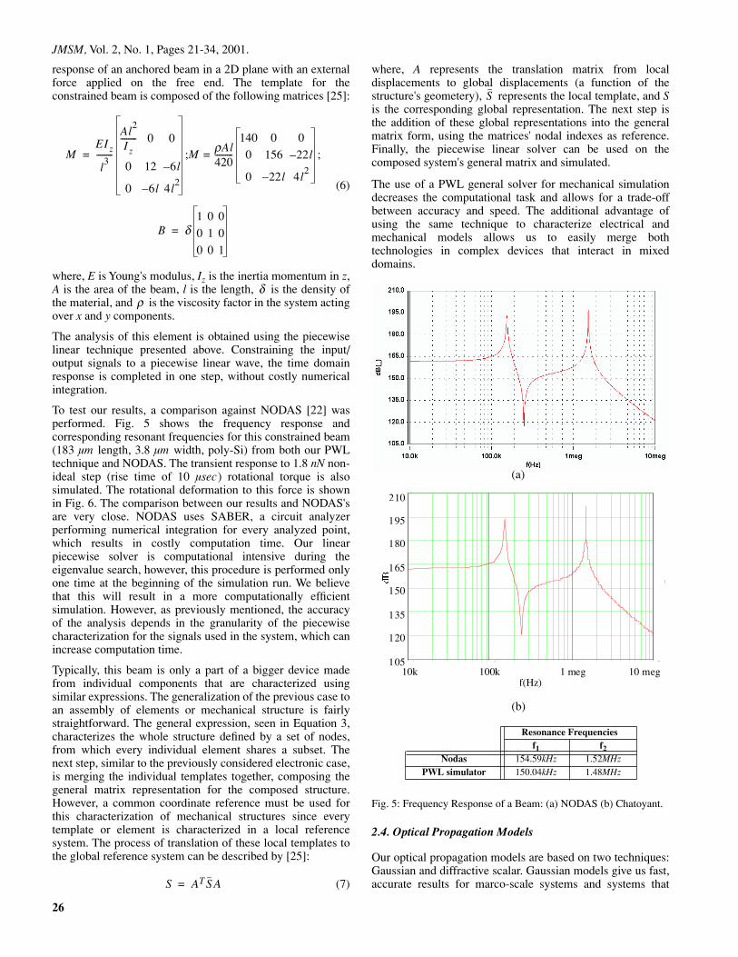
To test our results, a comparison against NODAS [22] wasperformed. Fig. 5 shows the frequency response andcorresponding resonant frequencies for this constrained beam(183 µm length, 3.8 µm width, poly-Si) from both our PWLtechnique and NODAS. The transient response to 1.8 nN non-ideal step (rise time of 10 µsec) rotational torque is alsosimulated. The rotational deformation to this force is shownin Fig. 6. The comparison between our results and NODAS'sare very close. NODAS uses SABER, a circuit analyzerperforming numerical integration for every analyzed point,which results in costly computation time. Our linearpiecewise solver is computational intensive during theeigenvalue search, however, this procedure is performed onlyone time at the beginning of the simulation run. We believethat this will result in a more computationally efficientsimulation. However, as previously mentioned, the accuracyof the analysis depends in the granularity of the piecewisecharacterization for the signals used in the system, which canincrease computation time.
Typically, this beam is only a part of a bigger device madefrom individual components that are characterized usingsimilar expressions. The generalization of the previous case toan assembly of elements or mechanical structure is fairlystraightforward. The general expression, seen in Equation 3,characterizes the whole structure defined by a set of nodes,from which every individual element shares a subset. Thenext step, similar to the previously considered electronic case,is merging the individual templates together, composing thegeneral matrix representation for the composed structure.However, a common coordinate reference must be used forthis characterization of mechanical structures since everytemplate or element is characterized in a local referencesystem. The process of translation of these local templates tothe global reference system can be described by [25]:
(7)
where, A represents the translation matrix from localdisplacements to global displacements (a function of thestructure's geometery), represents the local template, and Sis the corresponding global representation. The next step isthe addition of these global representations into the generalmatrix form, using the matrices' nodal indexes as reference.Finally, the piecewise linear solver can be used on thecomposed system's general matrix and simulated.
The use of a PWL general solver for mechanical simulationdecreases the computational task and allows for a trade-offbetween accuracy and speed. The additional advantage ofusing the same technique to characterize electrical andmechanical models allows us to easily merge bothtechnologies in complex devices that interact in mixeddomains.
Fig. 5: Frequency Response of a Beam: (a) NODAS (b) Chatoyant.
2.4. Optical Propagation Models
Our optical propagation models are based on two techniques:Gaussian and diffractive scalar. Gaussian models give us fast,accurate results for marco-scale systems and systems that
MEIz
l3
--------
Al2
Iz-------- 0 0
0 12 6l–
0 6l– 4l2
MρAl420---------
140 0 0
0 156 22l–
0 22l– 4l2
= ;;=
B δ1 0 0
0 1 0
0 0 1
=
δρ
S AT SA=
S
(b)
(a)
Resonance Frequenciesf1 f2
Nodas 154.59kHz 1.52MHzPWL simulator 150.04kHz 1.48MHz
4 5 6 7
10k 100k 1 meg 10 meg
210
195
180
165
150
135
120
105
f(Hz)

27
Modeling Optical MEM Systems
exhibit limited diffraction. Slower diffractive scalar modelsmust be used when diffraction effects dominate the system.
2.4.1. Gaussian models
The optical propagation is based on Gaussian beam analysis,allowing paraxial light to be modeled by nine scalarparameters, and components to be modeled by an opticalABCD matrix, which describes how light is effected by acomponent [1]. The Gaussian beam is defined by theparameters seen in Table 1.
As the parameters in the table discretely allude to, our opticalpropagation is actually a mixture of ray analysis and Gaussiananalysis. We first find the position and direction of the centerof the Gaussian beam, using typical ray methods. We then"superimpose" the Gaussian beam over this ray-traced beamto model intensity, waist, phase, and depth of focus. Theadvantage of using Gaussian beam analysis is in thecomputational speed in which propagated light can bemodeled. This allows for interactive system level design,however, for some micro systems, where diffractive effectsdominate, another optical propagation method has to be used,as seen later.
These nine scalar parameters are contained in Chatoyant'smessage class, and passed between components. It is thecomponent's responsibility to "construct" the beam from theparameters, alter the beam according to its function, and"decompose" the beam back into parameters, which arereturned to the message class and passed to the next object.Using Gaussian beam propagation, components are modeledwith the previously mentioned ABCD matrix. For example,we examine the interaction between a Gaussian beam and athin lens. To study the beam/lens interaction, we start with adefinition of the Gaussian beam's q-parameter, whichcharacterizes a Gaussian beam of known peak amplitude [26]:
, (8)
where, the real part is the distance to the minimum waist, andthe imaginary is the Rayleigh range, from which the waist ofthe beam is determined. The new Gaussian beam is definedby the following:
, (9)
where, ABCD is the matrix that defines a component. In thecase of a thin lens, A=1, B=0, C=-1/f, D=1, where f is thefocal length of the lens. Solving for q2, and determining thereal and imaginary parts, the new z0' and zw0' for theemerging Gaussian beam can be found:
(10)
(11)
The position and direction of the beam is determined fromcommon Ray tracing techniques:
(12)
Fig. 6: Transient Response of a Beam: (a) NODAS (b) Chatoyant.
However, as the systems that we wish to design continue todiminish in size, diffractive effects are a major concern. Forexample, in optical MEM design, the size of the components,apertures, and small structures bring diffractive effects intoplay, along with the use of diffractive elements such asFresnel zone plates, binary lenses, gratings, and computergenerated holograms (CGH) [27]. Therefore, new designtools are needed that utilize optical models that can provideaccurate diffractive results with reasonable computationalcosts. In addition to diffractive effects, other characteristics ofoptical signals are important, such as polarization, scattering,phase, frequency (wavelength) dependence, and dispersion.This last being a requirement for modeling fiber opticcomponents.
q zw0 jz0+=
q2
Aq1 B+
Cq1 D+--------------------=
z0′ f 2 z0⋅
f zw0–( )2 z02
+-----------------------------------------=
zw0′ f f zw0 zw02– z02–⋅( )
f zw0–( )2 z02
+-----------------------------------------------------------=
Table 1: Gaussian Beam Parameters.
Parameter Descriptionx,y Center position of the Gaussian beam
Rho, theta Directional cosines of the Gaussian beamIntensity Peak intensity of the Gaussian beam
z0 Rayleigh range, or depth of focusZw0 Distance to the next minimum waist
Lambda Wavelength of the lightPhase Phase of the central peak of the beam
y2 Ay1 Bθ1+= θ2 Cy1 Dθ1+=
0 10µ 20µ 30µ 40µ 50µ 60µ 70µ 80µ 90µ 100µ
0.3
0.27
0.24
0.21
0.18
0.15
0.12
0.09
0.06
0.03
0.0
rad
sec(b)
(a)

JMSM, Vol. 2, No. 1, Pages 21-34, 2001.
28
Fig. 7: Scalar Modeling Techniques.
2.4.2. Scalar diffractive models
A diffractive optical propagation methodology is required tomodel light propagating through small sized components andthe diffractive elements found in optical MEM systems. Toidentify which modeling technique is best suited for ourimplementation, we need to analyze the optical MEMsystems that we wish to model and evaluate the availableoptical propagation techniques. Current optical MEMsystems have component sizes of roughly ten to hundreds ofmicrons and propagation distances in the hundreds ofmicrons. With these sizes and distances on the order of ten toa thousand times the wavelength of light, optical diffractivemodels are required. Fig. 7 is a tree that begins at the top withthe vector wave equations, or Maxwell's equations, andbranches through the different abstraction levels of scalarmodeling techniques. Along the arrows, notes are addedstating the limitations and approximations that are made foreach formulation. We start our search for the appropriateoptical propagation method with scalar diffraction models,due to our intuition that these models will be accurate in theoptical MEM domain, and have a smaller computation timethan the full vector method.
Scalar equations are directly descended from Maxwell'sEquations. Maxwell equations, with the absence of freecharge, are [28-30]:
(13)
These equations can be recast into the following form:
(14)
If we assume that the dielectric medium is linear, isotropic,
homogeneous, and nondispersive, all components in theelectric and magnetic field can be summarized by the scalarwave equation:
(15)
For monochromatic light, U(P,t) is the positional complexwave function, where P is the position of a point in space:
(16)
By placing the positional complex wave function into thescalar wave equation, the result is the time-independentHelmholtz equation, which every scalar wave must satisfy:
, (17)
where,
The challenge is to determine the scalar wave function as itpropagates through a diffractive element. One answer is basedon the Huygens-Fresnel principle that states that everyunobstructed point of a wavefront at a given time serves as asource of spherical wavelets with the same frequency as theprimary wave. The Huygens-Fresnel principlemathematically describes the Rayleigh-Sommerfeld scalardiffraction formulation:
, (18)
where, and are the coordinates of the aperture plane, andx and y are the coordinates of the obsevation plane.
All scalar diffraction solutions are limited by twoassumptions; the diffracting structures must be "large"compared with the wavelength of the light and theobservation screen can not be "too close" to the diffracting
Vector Wave Equations – Maxwell Equations
Scalar Equations
Fresnel-Kirchoff Rayleigh-Sommerfeld
Fresnel Approximation Fraunhofer Approximation
Diffracting element >> λObservation plane not close to diffracting element
Boundary conditions on field strengthand normal derivative
Use for non-planar components
Boundary conditions on field strength ornormal derivative, since they are related
Use for planar components
Binomial expansion for the distance fromaperture to observation plane
Spherical wave replaced by quadraticphase exponential (parabolic fronts)
Quadratic phase exponential = 1Solve with Fourier Transform
∇ E× µ H∂t∂
-------–= ∇ H× ε E∂t∂
------–=
∇ εE• 0= ∇ µH• 0=
∇2En2
c2-----
t
2
∂∂
E– 0= ∇2Hn2
c2-----
t
2
∂∂
H– 0=
∇2Un2
c2-----
t
2
∂∂
U– 0=
U P t,( ) a P( )e jϕ P( )e j2πv=
∇2 k2+( )U P( ) 0=
k2πλ
-------=
U2 x y,( ) zjλ------ U1 ξ η,( )e jkr12
r122
------------- ξ η∂∂∫∫=
ξ η

29
Modeling Optical MEM Systems
structure. However, these dimensions are not clearly defined,questioning if scalar optical models are valid for all opticalMEM systems. For some extremely small optical MEMsystems, our initial intuition of "adequate" scalar models,might be invalid, and full wave propagation models must beused.
When modeling scalar formulations, explicit integration ofthe wave front is performed at each interface, severelyincreasing the computation time. Using approximations to thescalar formulations, as seen in Fig. 7, can reduce this time.For example, the Fraunhofer approximation is solved using aFourier transform, where common FFT algorithms enable anefficient solution. However, the valid propagation ranges limitwhen these approximations can be used. Fig. 8 shows wherethese different modeling techniques are valid with respect tothe distance propagated past a diffracting element.
Fig. 8: Valid Propagation Distances of Scalar Modeling Techinques.
Enabling diffraction propagation in Chatoyant requiresadditional parameters in the message class. The class nowcontains the user's requested optical propagation method (ray,Gauss, or scalar diffractive), along with the complexwavefront of the beam as it propagates through the system.The wavefront is gridded, defining the degree of accuracy ofthe model of the wave. As with the Gaussian propagation, it isthe component's responsibility to alter the wavefront as thecomponent interacts with the light beam and return the resultback into the message class.
We have currently implemented the Rayleigh-Sommerfelddiffractive formulation, using a 96-point Gaussian quadraturemethod for our integration technique. In Fig. 9, we showsimulation results of a 850 nm plane wave propagating thougha 50 µm aperture and striking an observation plane 300 µmaway. We compare our simulations with a "basecase" from MathCAD, which uses a Romberg integrationtechnique. The table in Fig. 9 shows the computation time andrelative error of the system (compared with the base case) fordifferent grid spacing. Using our integration technique we candecrease the computation time an order of magnitude and stillremain within 2% accuracy.
3. Simulations and Analyses Of Optical MEM Systems
In this section, we show how Chatoyant can model andsimulate complete mixed-signal systems. The first systemuses both electrical and optical signals to simulate a complete4f optoelectronic link. The second example, building from thetwo signal 4f link, adds mechanical signals for simulation andanalysis of an optical MEM system. This set of examplesystems is centered on an optical MEM scanning mirror. Withthis device we are able to simulate an optical scanning system
and a self-aligning optical detection system. These systemsshow Chatoyant's ability to model a mixed system ofmechanical MEMs, optics, and electronic feedback.
Fig. 9: Computation Time vs. Accuracy using Chatoyant's ScalarPropagation Models.
3.1. Full Link Example
A complete optoelectronic simulation of a 4f opticalcommunication link in Chatoyant is presented in Fig. 10. Thedistance between the VSCEL array and the first lens, and thedistance between the second lens and the detector array areboth 1 mm. The distance between the lenses is 2 mm, withboth lenses having a focal length of 1 mm. The top third of thefigure shows the system as represented in Chatoyant. Eachicon represents a component model, and each line representsa signal path (either optical or electrical) connecting theoutputs of one component to the inputs of the next. Several ofthe icons, such as the VCSELs and receivers, model theoptoelectronic components themselves, while others, such asthe output graph, are used to monitor and display the behaviorof the system. The input to the system is an electrical signalwith speed varying from 300 MHz to 1.5 GHz. A Gaussiannoise with variance of 0.5 V has been added to the multistagedriver system to show the ability of our models to respond toarbitrary waveforms.
In the center of the figure, three snapshots (before theVCSEL, after the VCSEL, and after the detector) show thebehavior of the CMOS drivers under a 300 MHz noisy signal.In these snapshots, one can see the amplification of thesystem noise through the CMOS drivers, the clipping of sub-threshold noise in the VCSEL, and the frequency response onthe quality of the received signal. This last observation isbetter seen in the three eye diagrams, shown in the bottom ofFig. 10, analyzed at 300 MHz, 900 MHz, and 1.5 GHz. For thecomponent values chosen, the system operates withreasonable BER up to about 1 GHz.
FresnelApproximation
FraunhoferApproximation
ScalarVector
Full WaveEquation
Rayleigh-SommerfeldFresnel-Kirchoff
λ>>z 3 22 ])()[(4
ηξπ −+−>> yxz2
)( max22 ηξ +>> kz
80 80×
300µm
200 200
80 80 40 40 20 20
80 80
Chatoyant MathCADTime(min) Error(%)* Time(min) Error(%)*
160x160 17.75 X X X80x80 4.45 0.637 120 040x40 .1 1.67 20 1.5420x20 0.29 3.37 7 4.32 *RMS Error of grid cells with respect to 80x80 MathCAD

JMSM, Vol. 2, No. 1, Pages 21-34, 2001.
30
Fig. 10: Chatoyant Analysis of an Opto-electronic 4f Communications Link.
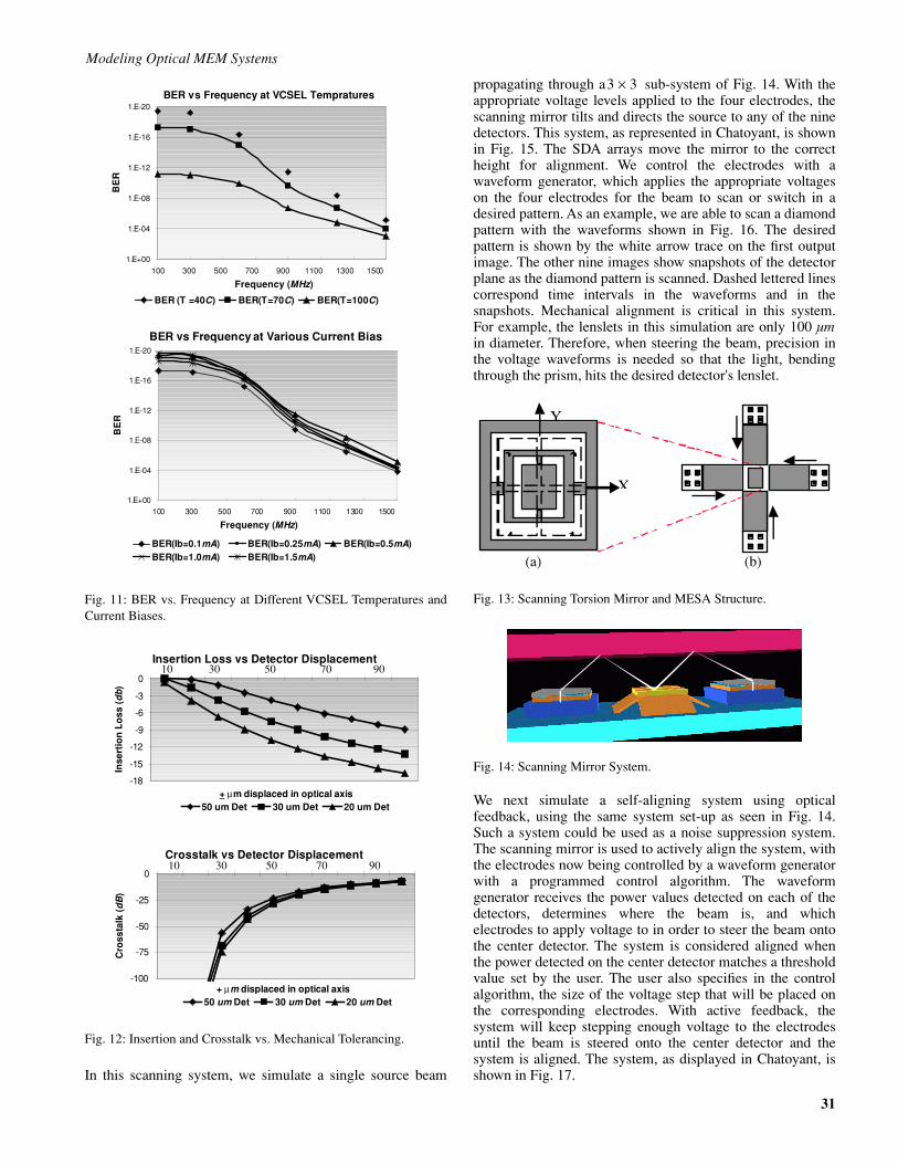
For this 4f system, the VCSEL and driver circuits explicitlymodel the effects of bias current and temperature on the L-Iefficiency of the lasers. Fig. 11 shows the effects oftemperature, T, and current bias, Ib, on the BER of the link.Generally, the frequency response of the link is dominated bythe design of the receiver circuit, however it is interesting tonote that both the VCSEL temperature and bias have asignificant effect on system performance, due to their impactin the power through the link. Perhaps most interesting is thefact that increasing bias current does not always correspond tobetter performance over the whole range of frequenciesexamined. Note that the curve for 1 mA bias offers the bestperformance below 600 MHz, however the 0.5 mA bias (thenominal threshold of the VCSEL), crosses the curve for 1 mAand achieves the best performance at higher frequencies.
As an example of our mechanical tolerancing, we analyze thesystem with varying sized photo-detectors (50, 30, and 20µm). The detectors are displaced from ±10 µm to ±100 µm indetector position along the axis of optical propagation. Thisresults in defocusing of the beam relative to the detectorarray. We calculate both the insertion loss and the worst caseoptical crosstalk as the detectors are displaced. The results areshown in Fig. 12. System components can be analyzed fortheir sensitivity to mechanical tolerances using our MonteCarlo tolerancing method described in [3,4].
Two additional optical analyses are also shown in theChatoyant representation in Fig. 10. The first is the beamprofile analysis, which graphically displays one beam's waistas it propagates between components, showing the possibilityof clipping at the lenses. The second analysis shows theoptical signals as they strike the detector array. This analysisalso gives the user the amount of optical power captured oneach of the detectors. From this analysis, optical crosstalk andsystem insertion loss can be calculated.
3.2. Optical Beam Steering/Alignment System
An optical MEM component that we have modeled inChatoyant and used in system level simulations is a torsion-scanning mirror. This is a micromachined 2D mirror builtupon a Micro Elevator by Self Assembly (MESA) structure[31,32]. The mirror and MESA structure are shown in Fig. 13(a) and (b), respectively. The scanning mirror can tilt alongthe torsion bars in both the x and y directions and is controlledelectrostatically through four electrodes beneath the mirror,outlined in Fig. 13 (a) by the dashed boxes. For example, themirror tilts in the positive x direction when voltage is appliedto electrodes 1 and 2, and the mirror tilts in the negative ydirection when voltage is applied to electrodes 1 and 4. TheMESA structure is shown in Fig. 13 (b). The mirror iselevated by four scratch drive accuators (SDA) [33] setspushing the support plates together, allowing for the scanningmirror to buckle and rise up off the substrate. The MESAstructure's height is required to be large enough such that thetilt of the mirror will not cause the mirror to hit the substrate.System alignment can also be possibly aided by this MESAstructure.
Fig. 14 shows the torsion-scanning mirror system that we aresimulating with Chatoyant. VCSELs emit light verticallythrough a prism and reflects off a plane mirror. The light isthen reflected off of the optical MEM scanning mirror, backto the plane mirror, and captured through a prism ontodetectors. With the flexibility of the scanning mirror, thissystem could act as a switch, an optical scanner, or areconfigurable optical interconnect. We have simulatedsystems using this scanning mirror configuration forswitching and self-alignment through optical feedback. Wefirst demonstrate an optical scanning system.
DIGITAL DRIVER
VCSEL
4f Optical System
(300 MHz)
Receiver
Gaussian Waist Analysis
Power Analysis
31
Modeling Optical MEM Systems
Fig. 11: BER vs. Frequency at Different VCSEL Temperatures andCurrent Biases.
Fig. 12: Insertion and Crosstalk vs. Mechanical Tolerancing.
In this scanning system, we simulate a single source beam
propagating through a sub-system of Fig. 14. With theappropriate voltage levels applied to the four electrodes, thescanning mirror tilts and directs the source to any of the ninedetectors. This system, as represented in Chatoyant, is shownin Fig. 15. The SDA arrays move the mirror to the correctheight for alignment. We control the electrodes with awaveform generator, which applies the appropriate voltageson the four electrodes for the beam to scan or switch in adesired pattern. As an example, we are able to scan a diamondpattern with the waveforms shown in Fig. 16. The desiredpattern is shown by the white arrow trace on the first outputimage. The other nine images show snapshots of the detectorplane as the diamond pattern is scanned. Dashed lettered linescorrespond time intervals in the waveforms and in thesnapshots. Mechanical alignment is critical in this system.For example, the lenslets in this simulation are only 100 µmin diameter. Therefore, when steering the beam, precision inthe voltage waveforms is needed so that the light, bendingthrough the prism, hits the desired detector's lenslet.
Fig. 13: Scanning Torsion Mirror and MESA Structure.
Fig. 14: Scanning Mirror System.
We next simulate a self-aligning system using opticalfeedback, using the same system set-up as seen in Fig. 14.Such a system could be used as a noise suppression system.The scanning mirror is used to actively align the system, withthe electrodes now being controlled by a waveform generatorwith a programmed control algorithm. The waveformgenerator receives the power values detected on each of thedetectors, determines where the beam is, and whichelectrodes to apply voltage to in order to steer the beam ontothe center detector. The system is considered aligned whenthe power detected on the center detector matches a thresholdvalue set by the user. The user also specifies in the controlalgorithm, the size of the voltage step that will be placed onthe corresponding electrodes. With active feedback, thesystem will keep stepping enough voltage to the electrodesuntil the beam is steered onto the center detector and thesystem is aligned. The system, as displayed in Chatoyant, isshown in Fig. 17.
BER vs Frequency at Various Current Bias1.E-20
1.E-16
1.E-12
1.E-08
1.E-04
1.E+00100 300 500 700 900 1100 1300 1500
Frequency (MHz)
BE
R
BER(Ib=0.1mA) BER(Ib=0.25mA) BER(Ib=0.5mA)BER(Ib=1.0mA) BER(Ib=1.5mA)
BER vs Frequency at VCSEL Tempratures1.E-20
1.E-16
1.E-12
1.E-08
1.E-04
1.E+00100 300 500 700 900 1100 1300 1500
Frequency (MHz)
BE
R
BER (T =40C) BER(T=70C) BER(T=100C)
Insertion Loss vs Detector Displacement
-18
-15
-12
-9
-6
-3
0
+ µm displaced in optical axis
Inse
rtio
n L
oss
(d
b)
50 um Det 30 um Det 20 um Det
Crosstalk vs Detector Displacement
-100
-75
-50
-25
0
+ µm displaced in optical axis
Cro
ssta
lk (
dB
)
50 um Det 30 um Det 20 um Det
10 30 50 70 90
10 30 50 70 90
3 3×
1
23
4
X
Y
(a) (b)

JMSM, Vol. 2, No. 1, Pages 21-34, 2001.
32
Fig. 15: Scanning System Represented in Chatoyant.
Fig. 16: Scanning Waveforms and Scanned Diamond Pattern.
To simulate this self-aligning system, we introduced randomoffsets in the lenses and in the VCSEL position and observeas the beam moves towards focus on the center detector.Snapshots of the image at the detectors are given in Figure 18
for three cases. The first results, shown in Figure 18(a), iswhen the second lens is offset 35 µm in the x direction. Figure18(b) shows the results of the second lenslet offset in both the-x and y direction by 35 µm . The final case has both lensesoffset. The first is offset by 5 µm in the x direction, and thesecond lens is offset by 35 µm in the -x direction and 5 µm inthe y direction. The results are seen in Figure 18(c). Noticethat the beam on the final images is not exactly in the centerof the middle detector. This is due to the power being detectedat this point exceeding the power threshold (98.6%) we set foralignment.
4. Summary and Conclusions
Multi-domain modeling and multi-rate simulation tools arerequired to support mixed technology system design. Thispaper has shown Chatoyant's support for simulating andanalyzing optical MEM systems with models for optical,electrical, and mechanical models for components andsignals. By supporting a variety of component and signalmodeling techniques and multiple abstraction levels,Chatoyant has the ability to perform and analyze mixed-signal trade-offs, which makes it valuable to optical MEMdesigners. Keeping simulations, along with analysistechniques such as Monte Carlo for mechanical tolerancing,BER, crosstalk, and insertion loss, within the Chatoyantframework allows for quick and efficient analysis throughoutmultiple domains.
Acknowledgments
This work was supported by DARPA, under Grant No.F3602-97-2-0122 and NSF, under Grant No. ECS-9616879.
Fig. 17: Self-aligning System Using Optical Feedback.
Electrode 1Electrode 4
Electrode 3 Electrode 2
A B C D EA B C D E
A B
C D E
33
Modeling Optical MEM Systems
Fig. 18: Self alignment Results.
References
[1] S. P. Levitan, T. P. Kurzweg, P. J. Marchand, M. A.Rempel, D. M. Chiarulli, J. A. Martinez, J. M. Brid-gen, C. Fan, F. B. McCormick, "Chatoyant: a com-puter-aided design tool for free-space optoelectronicsystems," Applied Optics, Vol. 37, No. 26, September,1998, pp. 6078-6092.
[2] S. P. Levitan, P. J. Marchand, T. P. Kurzweg, M. A.Rempel, D. M. Chiarulli, C. Fan, F. B. McCormick,"Computer-Aided Design of Free-Space Opto-Elec-tronic Systems," Proceedings of the 1997 DesignAutomation Conference, Anaheim, CA, June 1997,Best Paper Award, pp. 768-773.
[3] T. P. Kurzweg, S. P. Levitan, P. J. Marchand, J. A.Martinez, K. R. Prough, D. M. Chiarulli, "CAD forOptical MEMS," Proceedings of the 36th IEEE/ACMDesign Automation Conference (DAC'99), NewOrleans, LA, June 20-25, 1999.
[4] T. P. Kurzweg, S. P. Levitan, P. J. Marchand, J. A.Martinez, K. R. Prough, D. M. Chiarulli., "Modelingand Simulating Optical MEMS using Chatoyant,"Design, Test, and Microfabrication of MEMS/MOEMS, Paris, France, March 30 - April 1, 1999.
[5] J. A. Martinez, S. P. Levitan, T. P. Kurzweg, E. N.Reiss, M. T. Shomsky, P. J. Marchand, D. M.Chiarulli, "Modeling Free Space Optoelectronic Inter-
connects," IEEE Conference on Parallel Interconnects(PI'99), Anchorage, Alaska, October 17-19, 1999.
[6] J. Buck, S. Ha, E. A. Lee, Messerschmitt, D.,"Ptolemy: a framework for simulating and prototypingheterogeneous systems," Int. J. Computer Simulation,Vol. 4, 1994, pp. 155-182.
[7] J. Morikuni, S. Kang, Computer -Aided Design ofOptoelectronic Integrated Circuits and Systems, Pren-tice-Hall, Inc., New Jersey, Chapter 6, 1997.
[8] E. M. Buturla, P. E. Cottrell, B. M. Grossman, K. A.Salsburg, "Finite element analysis of semiconductordevices: the FIELDAY program," IBM Journal ofResearch and Development, vol. 25, 1981, pp. 218-231.
[9] M. R. Pinto, C. S. Rafferty, R. W. Dutton, "PISCES II- Poisson and continuity equation solver," StanfordElectronics Laboratory Technical Report, StandardUniversity, September 1984.
[10] P. C. H Chan and C. T. Sah, "Exact equivalent circuitmodel for steady-state characterization of semicon-ductor devices with multiple energy-level recombina-tion centers," IEEE Transactions of ElectronicDevices, Vol. ED-26, 1979, pp. 924-936.
[11] R. Kielkowski, "SPICE, Overcoming the obstacles ofcircuit simulation," McGraw-Hill, Inc., chapter 4.1994.
[12] S. Kim, N. Gopal, L. T. Pillage, "Time-Domain Mac-romodels for VLSI Interconnect Analysis," IEEE Tran.
Time
Time
(a)
(b)
(c)
JMSM, Vol. 2, No. 1, Pages 21-34, 2001.
34
on CAD of Integrated Circuits and Systems, Vol. 13,No. 10, pp. 1257-1270, October 1994.
[13] A. Devgan and R. A. Rohrer, "Adaptively ControlledExplicit Simulation," IEEE Tran. on CAD of Inte-grated Circuits and Systems, pp. 746-762, June 1994.
[14] P. Feldmann and R. W. Freund, "Efficient linear circuitanalysis by PadÈ approximation via the Lanczos pro-cess," IEEE Trans. Computer-Aided Design, vol. 14,pp. 639-649, May. 1995.
[15] A. Odabasioglu, M. Celik, L. T. Pileggi, "PRIMA:Passive Reduced-Order Interconnect MacromodelingAlgorithm," IEEE Trans. Computer-Aided Design,vol. 17, No. 8, 1998, pp 645-654.
[16] L. T. Pillage and R. A. Rohrer, "Asymptotic waveformevaluation for timing analysis," IEEE Trans. Com-puter-Aided Design, vol. 9, No. 4, pp. 352-366, Apr.1990.
[17] L. W. Nagel,"SPICE2, a computer program to simu-late semiconductor circuits," Tech. Rep. Memo UCB/ERL M520, Univ. of California, Berkeley, CA, May1975.
[18] A. Salz and M. Horowitz, "IRSIM: an IncrementalMOS Switch-Level Simulator," Proceedings of the26th Design Automation Conference, pp. 173-178,1989.
[19] R. Kao and M. Horowitz, "Timing Analysis for Piece-wise Linear Rsim," IEEE Trans. Computer-AidedDesign, vol. 13, No. 12, 1994, pp 1498-1512.
[20] J. Vlach and K. Singhai, Computer Methods for Cir-cuit Analysis and Design.
[21] J. Clark, N. Zhou, S. Brown, and K. S. J. Pister,"Nodal Analysis for MEMS Simulation and Design,"Proc. Modeling and Simulation of MicrosystemsWorkshop, Santa Clara, CA, April 6-8, 1998.
[22] J. E. Vandemeer, "Nodal Design of Actuators and Sen-sors (NODAS)", M.S. Thesis, (Department of Electri-cal and Computer Engineering, Carniege MellonUniversity, Pittsburgh, PA., 1997).
[23] J. E. Vandemeer, M. S. Kranz, G. K. Fedder, "Hierar-chical Representation and Simulation of Microma-chined Inertial Sensors," Proc. Modeling andSimulation of Microsystems Workshop, Santa Clara,CA, April 6-8, 1998.
[24] W. J. Duncan, "Reciprocation of Triply PartitionedMatricies," J. Roy. Aeron. Soc., vol. 60, 1956, pp. 131-132.
[25] J. S. Przemieniecki, Theory of Matrix Structural Anal-ysis, (McGraw-Hill, New York, New York, 1968).
[26] B. E. A Saleh and M. C. Teich, Fundamentals of Pho-tonics (New York: Wiley-Interscience, 1991).
[27] S. J. Walker and D. J. Nagel, "Optics & MEMS,"Navel Research Lab, NRL/MR/6336-99-7975
[28] M. Born, E. Wolf, Principles of Optics, (PergamonPress, 1959).
[29] J. W. Goodman, Introduction to Fourier Optics, Sec-ond Edition (The McGraw-Hill Companies, Inc.,1996).
[30] E. Hecht, Optics, Second Edition (Addison-WesleyPublishing Company, 1987).
[31] M. C. Wu, "Micromachining for optical and Optoelec-tronic Systems," Proceedings of the IEEE, Vol. 85, No.11, (November 1997), pp. 1833-1856.
[32] W. Piyawattanametha, L. Fan, S. S. Lee, J. G. D. Su,M. C. Wu, "MEMS Technology for Optical Crosslinkfor Micro/Nano Satellites," International Conferenceof Integrated Nano/Microtechnolgy for Space Appli-cations (NANOSPACE98), NASA/Johnson SpaceCenter, Houston, TX, Nov 1-6, 1998.
[33] T. Akiyama, D. Collard, H. Fujita, "Scratch drive actu-ator with mechanical links for self-assembly of three-dimensional MEMS," Journal of Microelectromechan-ical Systems, Vol. 6, No. 1., March 1997, pp. 10-17.
Received in Cambridge, MA, USA, November 13 1999
Paper 2/01775
Related Documents