Institut für integrierte Systeme Integrated Systems Laboratory Modeling of Leakage Currents in Ultra Shallow Junctions Andreas Schenk, Artur Scheinemann ETH Zürich, Integrated Systems Laboratory

Welcome message from author
This document is posted to help you gain knowledge. Please leave a comment to let me know what you think about it! Share it to your friends and learn new things together.
Transcript
Institut für integrierte Systeme Integrated Systems Laboratory
Modeling of Leakage Currents in Ultra
Shallow Junctions
Andreas Schenk, Artur Scheinemann
ETH Zürich, Integrated Systems Laboratory
Institut für integrierte Systeme Integrated Systems Laboratory ETH Zürich
E-MRS, Strasbourg, 28.5.2013
A.Schenk – [email protected]
2
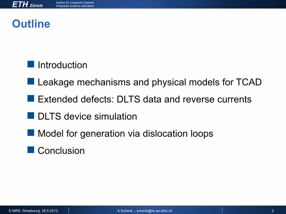
Outline
Introduction
Leakage mechanisms and physical models for TCAD
Extended defects: DLTS data and reverse currents
DLTS device simulation
Model for generation via dislocation loops
Conclusion
Institut für integrierte Systeme Integrated Systems Laboratory ETH Zürich
E-MRS, Strasbourg, 28.5.2013
A.Schenk – [email protected]
3
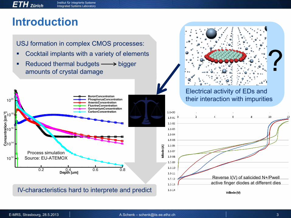
Introduction
Electrical activity of EDs and
their interaction with impurities
? USJ formation in complex CMOS processes:
Cocktail implants with a variety of elements
Reduced thermal budgets bigger
amounts of crystal damage
IV-characteristics hard to interprete and predict
Reverse I(V) of salicided N+/Pwell
active finger diodes at different dies
Process simulation
Source: EU-ATEMOX
Institut für integrierte Systeme Integrated Systems Laboratory ETH Zürich
E-MRS, Strasbourg, 28.5.2013
A.Schenk – [email protected]
4
Leakage mechanisms and physical
models for TCAD
Institut für integrierte Systeme Integrated Systems Laboratory ETH Zürich
E-MRS, Strasbourg, 28.5.2013
A.Schenk – [email protected]
5
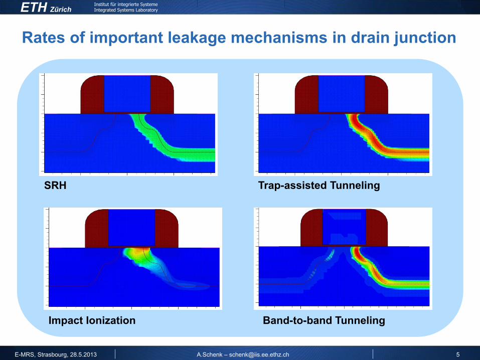
Rates of important leakage mechanisms in drain junction
SRH
Impact Ionization
Trap-assisted Tunneling
Band-to-band Tunneling
Institut für integrierte Systeme Integrated Systems Laboratory ETH Zürich
E-MRS, Strasbourg, 28.5.2013
A.Schenk – [email protected]
6
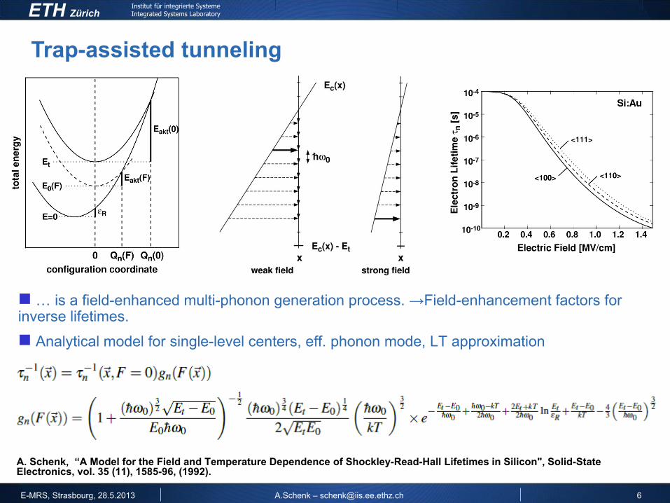
Trap-assisted tunneling
A. Schenk, “A Model for the Field and Temperature Dependence of Shockley-Read-Hall Lifetimes in Silicon", Solid-State Electronics, vol. 35 (11), 1585-96, (1992).
… is a field-enhanced multi-phonon generation process. →Field-enhancement factors for inverse lifetimes.
Analytical model for single-level centers, eff. phonon mode, LT approximation
Institut für integrierte Systeme Integrated Systems Laboratory ETH Zürich
E-MRS, Strasbourg, 28.5.2013
A.Schenk – [email protected]
7
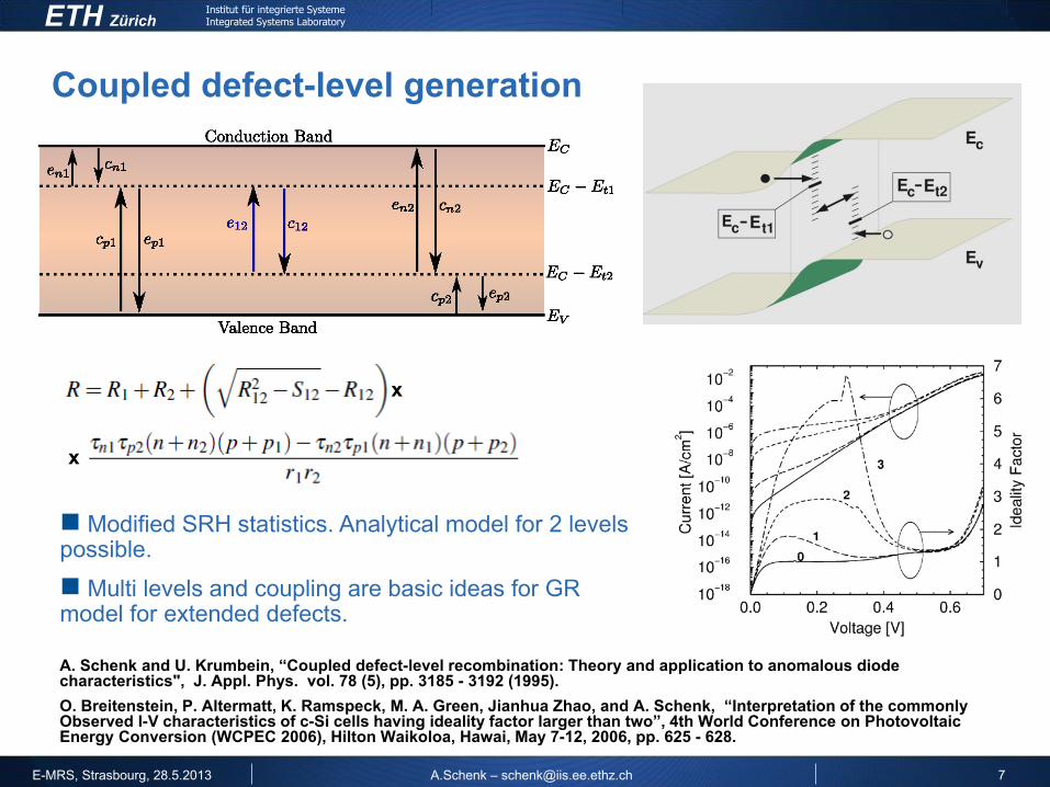
Coupled defect-level generation
Modified SRH statistics. Analytical model for 2 levels possible.
Multi levels and coupling are basic ideas for GR model for extended defects.
A. Schenk and U. Krumbein, “Coupled defect-level recombination: Theory and application to anomalous diode characteristics", J. Appl. Phys. vol. 78 (5), pp. 3185 - 3192 (1995).
O. Breitenstein, P. Altermatt, K. Ramspeck, M. A. Green, Jianhua Zhao, and A. Schenk, “Interpretation of the commonly Observed I-V characteristics of c-Si cells having ideality factor larger than two”, 4th World Conference on Photovoltaic Energy Conversion (WCPEC 2006), Hilton Waikoloa, Hawai, May 7-12, 2006, pp. 625 - 628.
x
x
Institut für integrierte Systeme Integrated Systems Laboratory ETH Zürich
E-MRS, Strasbourg, 28.5.2013
A.Schenk – [email protected]
8
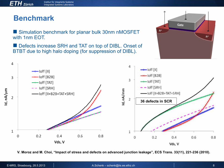
Simulation benchmark for planar bulk 30nm nMOSFET with 1nm EOT.
Defects increase SRH and TAT on top of DIBL. Onset of BTBT due to high halo doping (for suppression of DIBL).
V. Moroz and M. Choi, “Impact of stress and defects on advanced junction leakage”, ECS Trans. 33(11), 221-236 (2010).
36 defects in SCR
Benchmark

Institut für integrierte Systeme Integrated Systems Laboratory ETH Zürich
E-MRS, Strasbourg, 28.5.2013
A.Schenk – [email protected]
9
Extended defects: DLTS data and
reverse currents

Institut für integrierte Systeme Integrated Systems Laboratory ETH Zürich
E-MRS, Strasbourg, 28.5.2013
A.Schenk – [email protected]
10
Source:
Claverie et. Al., Materials Science in Semiconductor
Processing 3, (2000)
Calvo et. Al., NIM B (2004)
K. Sumino, Materials Science & Engineering B (2000)
Zoo of Extended Defects
Dislocation Loops {311} defects
Copper precipitates
on dislocations Stacking faults
Complex variety of extended defects with dependence on
Implant conditions
Thermal budget
Mechanical stress
Interactions with point-like defects contained in the crystal
Institut für integrierte Systeme Integrated Systems Laboratory ETH Zürich
E-MRS, Strasbourg, 28.5.2013
A.Schenk – [email protected]
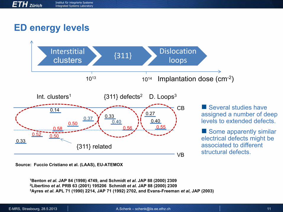
ED energy levels
1Benton et al. JAP 84 (1998) 4749, and Schmidt et al. JAP 88 (2000) 2309 2Libertino et al. PRB 63 (2001) 195206 Schmidt et al. JAP 88 (2000) 2309 3Ayres et al. APL 71 (1990) 2214, JAP 71 (1992) 2702, and Evans-Freeman et al, JAP (2003)
Interstitial clusters
{311} Dislocation
loops
Implantation dose (cm-2) 1014 1013
0.52 0.50 0.33
VB
CB
0.58
0.37 0.50
0.14
0.40
0.27
0.40
0.55 0.56
0.33
Int. clusters1 {311} defects2 D. Loops3
{311} related
Several studies have assigned a number of deep levels to extended defects.
Some apparently similar electrical defects might be associated to different structural defects.
Source: Fuccio Cristiano et al. (LAAS), EU-ATEMOX
11
Institut für integrierte Systeme Integrated Systems Laboratory ETH Zürich
E-MRS, Strasbourg, 28.5.2013
A.Schenk – [email protected]
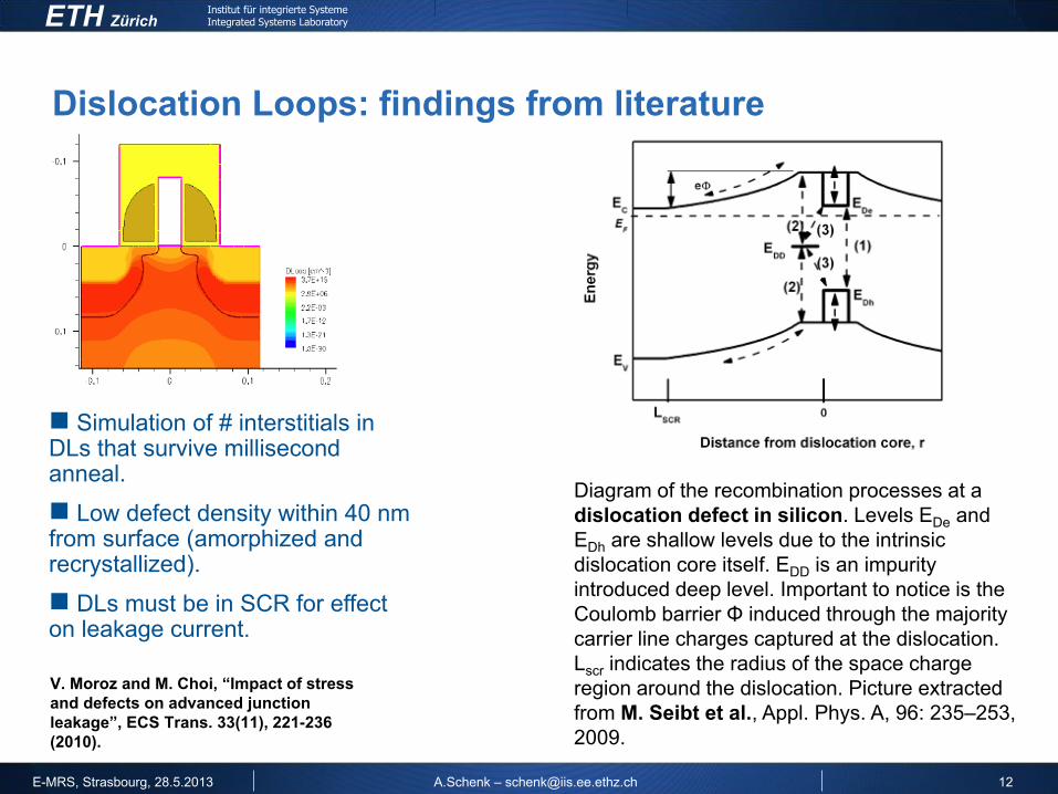
Dislocation Loops: findings from literature
V. Moroz and M. Choi, “Impact of stress
and defects on advanced junction
leakage”, ECS Trans. 33(11), 221-236
(2010).
Simulation of # interstitials in DLs that survive millisecond anneal.
Low defect density within 40 nm from surface (amorphized and recrystallized).
DLs must be in SCR for effect on leakage current.
Diagram of the recombination processes at a
dislocation defect in silicon. Levels EDe and
EDh are shallow levels due to the intrinsic
dislocation core itself. EDD is an impurity
introduced deep level. Important to notice is the
Coulomb barrier Φ induced through the majority
carrier line charges captured at the dislocation.
Lscr indicates the radius of the space charge
region around the dislocation. Picture extracted
from M. Seibt et al., Appl. Phys. A, 96: 235–253,
2009.
12
Institut für integrierte Systeme Integrated Systems Laboratory ETH Zürich
E-MRS, Strasbourg, 28.5.2013
A.Schenk – [email protected]
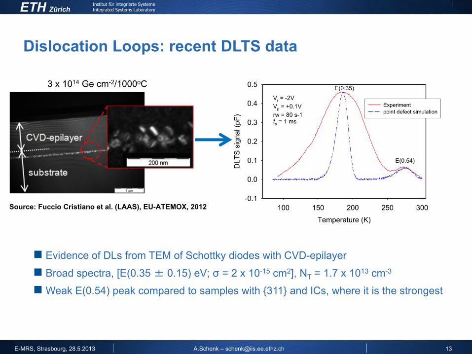
Dislocation Loops: recent DLTS data
3 x 10¹⁴ Ge cm-2/1000oC
Temperature (K)
100 150 200 250 300
DLT
S s
ignal (p
F)
-0.1
0.0
0.1
0.2
0.3
0.4
0.5
Experiment
point defect simulation
E(0.35)
E(0.54)
Vr = -2V
Vp = +0.1V
rw = 80 s-1tp = 1 ms
Evidence of DLs from TEM of Schottky diodes with CVD-epilayer
Broad spectra, [E(0.35 ± 0.15) eV; σ = 2 x 10-15 cm2], NT = 1.7 x 1013 cm-3
Weak E(0.54) peak compared to samples with {311} and ICs, where it is the strongest
Source: Fuccio Cristiano et al. (LAAS), EU-ATEMOX, 2012
13
Institut für integrierte Systeme Integrated Systems Laboratory ETH Zürich
E-MRS, Strasbourg, 28.5.2013
A.Schenk – [email protected]
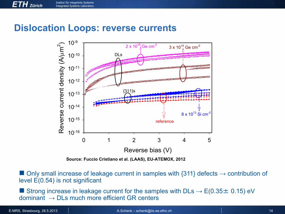
Dislocation Loops: reverse currents
Only small increase of leakage current in samples with {311} defects → contribution of level E(0.54) is not significant
Strong increase in leakage current for the samples with DLs → E(0.35± 0.15) eV dominant → DLs much more efficient GR centers
Source: Fuccio Cristiano et al. (LAAS), EU-ATEMOX, 2012
Reverse bias (V)
0 1 2 3 4 5
Revers
e c
urr
ent density (
A/
m2)
10-16
10-15
10-14
10-13
10-12
10-11
10-10
10-9
8 x 10¹³
Si cm-2
reference
DLs
{311}s
3 x 10¹⁴
Ge cm-22 x 10
15 Ge cm
-2
14

Institut für integrierte Systeme Integrated Systems Laboratory ETH Zürich
E-MRS, Strasbourg, 28.5.2013
DLTS device simulation
15

Institut für integrierte Systeme Integrated Systems Laboratory ETH Zürich
E-MRS, Strasbourg, 28.5.2013
A.Schenk – [email protected]
16
Transient Spectroscopy (principle)
Arrhenius shift in
Temperature of
iso-occupational
lines

Institut für integrierte Systeme Integrated Systems Laboratory ETH Zürich
E-MRS, Strasbourg, 28.5.2013
A.Schenk – [email protected]
17
Defect Occupation
Analytical solution by omission of:
Transition between occupied / unoccupied state is governed by microscopic properties
of the defect: ET , σn,p

Institut für integrierte Systeme Integrated Systems Laboratory ETH Zürich
E-MRS, Strasbourg, 28.5.2013
A.Schenk – [email protected]
18
Analytical solution is only valid under simplifying assumptions:
■ en » ep, cn, cp or at least eν » cν, otherwise free carrier profiles needed.
■ For different coupled defect species no analytical solution is possible.
■ Spatial distribution of defect profiles NT(r) can not be evaluated.
Numerical integration of from initial condition
Simple numerical integration
of n(t,T) leaving NT constant
and omitting carrier capture
Using carrier and defect
profiles obtained by process
and device simulation to run
integration on 1D/2D device
Use of advanced device
simulation software for
transient simulations of
DLTS profiles
Defect Occupation (2)

Institut für integrierte Systeme Integrated Systems Laboratory ETH Zürich
E-MRS, Strasbourg, 28.5.2013
A.Schenk – [email protected]
19
Defect Occupation (3)
10 uncoupled levels around ET = EC – 0.35 eV, NT,i = 1e12 cm-3, σn = 1e-15 cm2.
Distributed over energy interval ΔE.
With increasing ΔE the DLTS peak broadens and slightly shifts to lower T.
Sentaurus-Device DLTS simulation of Schottky diode with CVD-epilayer:
Shift of the level ET from mid-gap to EC shifts the DLTS peak to lower temperatures. Reason: Tmax “~” EC - ET
Peak height reaches a maximum where ET EF. Reason: also hole and capture processes in transient device simulation.

Institut für integrierte Systeme Integrated Systems Laboratory ETH Zürich
E-MRS, Strasbourg, 28.5.2013
A.Schenk – [email protected]
20
0
1e-12
2e-12
3e-12
4e-12
5e-12
150 200 250 300 350
DLT
S [
pF
]
Temperature [K]
Varying CouplingUncoupled Signal
0.1
1
10
100
1000
Co
up
lin
g [
1/s]
Coupling of 2 defect levels
Numerical integration is easily extended to 2 defect levels with mutual coupling.
ET1 = EC – 0.35 eV, ET2 = EC – 0.55 eV, N1 = 1e12 cm-3, N2 = 1.5e12 cm-3 , σn = 1e-15 cm2
With increasing coupling strength one DLTS peak is “absorbed” by the peak closest to the band. → Peak of the mid-gap level disappears.

Institut für integrierte Systeme Integrated Systems Laboratory ETH Zürich
E-MRS, Strasbourg, 28.5.2013
A.Schenk – [email protected]
21
Coupling of L defect levels
10 coupled levels around ET = EC – 0.35 eV, NT,i = 1e12 cm-3, σn = 1e-15 cm2.
With increasing coupling rate the peak height grows up to x2 and the maximum shifts to the position of the peak closest to the band.

Institut für integrierte Systeme Integrated Systems Laboratory ETH Zürich
E-MRS, Strasbourg, 28.5.2013
A.Schenk – [email protected]
22
Model for generation via dislocation
loops
Institut für integrierte Systeme Integrated Systems Laboratory ETH Zürich
E-MRS, Strasbourg, 28.5.2013
A.Schenk – [email protected]
23
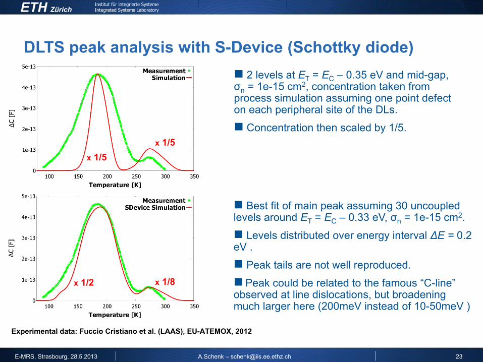
DLTS peak analysis with S-Device (Schottky diode)
Experimental data: Fuccio Cristiano et al. (LAAS), EU-ATEMOX, 2012
2 levels at ET = EC – 0.35 eV and mid-gap, σn = 1e-15 cm2, concentration taken from process simulation assuming one point defect on each peripheral site of the DLs.
Concentration then scaled by 1/5.
x 1/5
x 1/2
Best fit of main peak assuming 30 uncoupled levels around ET = EC – 0.33 eV, σn = 1e-15 cm2.
Levels distributed over energy interval ΔE = 0.2 eV .
Peak tails are not well reproduced.
Peak could be related to the famous “C-line” observed at line dislocations, but broadening much larger here (200meV instead of 10-50meV )
x 1/8
x 1/5
Institut für integrierte Systeme Integrated Systems Laboratory ETH Zürich
E-MRS, Strasbourg, 28.5.2013
A.Schenk – [email protected]
24
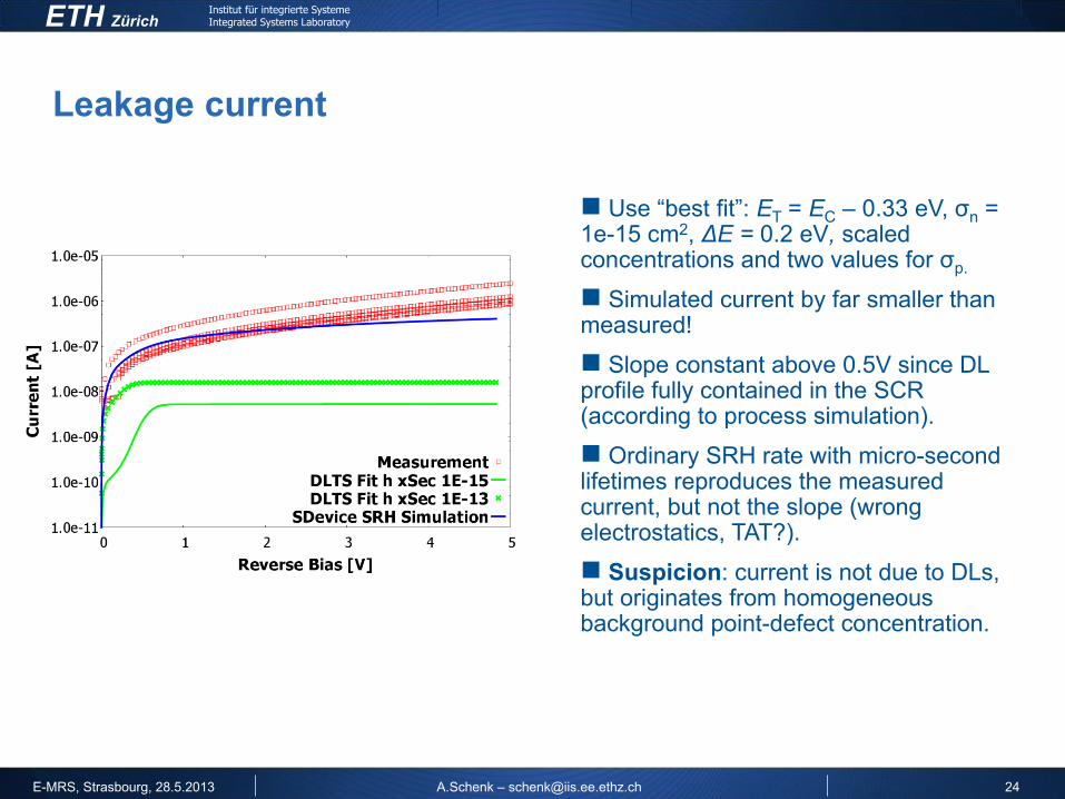
Leakage current
Use “best fit”: ET = EC – 0.33 eV, σn = 1e-15 cm2, ΔE = 0.2 eV, scaled concentrations and two values for σp.
Simulated current by far smaller than measured!
Slope constant above 0.5V since DL profile fully contained in the SCR (according to process simulation).
Ordinary SRH rate with micro-second lifetimes reproduces the measured current, but not the slope (wrong electrostatics, TAT?).
Suspicion: current is not due to DLs, but originates from homogeneous background point-defect concentration.
Institut für integrierte Systeme Integrated Systems Laboratory ETH Zürich
E-MRS, Strasbourg, 28.5.2013
A.Schenk – [email protected]
25
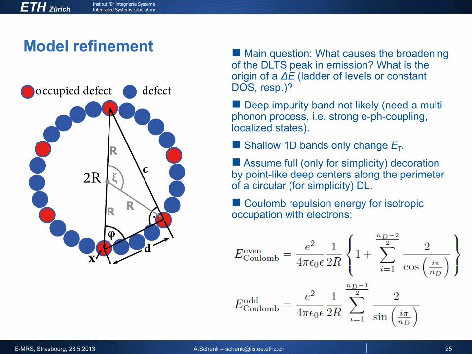
Model refinement Main question: What causes the broadening of the DLTS peak in emission? What is the origin of a ΔE (ladder of levels or constant DOS, resp.)?
Deep impurity band not likely (need a multi-phonon process, i.e. strong e-ph-coupling, localized states).
Shallow 1D bands only change ET.
Assume full (only for simplicity) decoration by point-like deep centers along the perimeter of a circular (for simplicity) DL.
Coulomb repulsion energy for isotropic occupation with electrons:
Institut für integrierte Systeme Integrated Systems Laboratory ETH Zürich
E-MRS, Strasbourg, 28.5.2013
A.Schenk – [email protected]
26
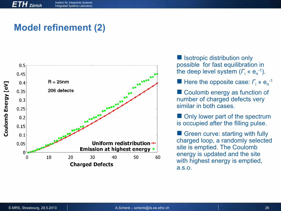
Model refinement (2)
Isotropic distribution only possible for fast equilibration in the deep level system (Γi « en
-1).
Here the opposite case: Γi » en-1
Coulomb energy as function of number of charged defects very similar in both cases.
Only lower part of the spectrum is occupied after the filling pulse.
Green curve: starting with fully charged loop, a randomly selected site is emptied. The Coulomb energy is updated and the site with highest energy is emptied, a.s.o.

Institut für integrierte Systeme Integrated Systems Laboratory ETH Zürich
E-MRS, Strasbourg, 28.5.2013
A.Schenk – [email protected]
27
Model refinement (3)
DLTS simulation of the Schottky diode with all quantities extracted from Sentaurus-Device.
Cascade process from Coulomb levels assumed.
ET = EC – 0.35 eV, σn = 1e-15 cm2, R & profile from process simulation
Broadening and energetic shift.
New ET would be EC – 0.4 eV

Institut für integrierte Systeme Integrated Systems Laboratory ETH Zürich
E-MRS, Strasbourg, 28.5.2013
A.Schenk – [email protected]
28
Conclusion
Institut für integrierte Systeme Integrated Systems Laboratory ETH Zürich
E-MRS, Strasbourg, 28.5.2013
A.Schenk – [email protected]
29
Conclusion
Based on the information of one broadened DLTS peak we suggest:
The generation behavior of DLs is due to decoration with point-like
defects along the perimeter (transition metals, oxygen,…).
The states of trapped electrons are localized.
The proximity of the trapped point charges causes a (non-
equidistant) Coulomb ladder of energy levels (Coulomb repulsion,
Hartree energy).
During release pulse electrons are emitted in a cascade process so
that the highest occupied energy level moves downwards.
This results in the observed broadening, but also in a deeper
ground state energy ET.

Institut für integrierte Systeme Integrated Systems Laboratory ETH Zürich
E-MRS, Strasbourg, 28.5.2013
A.Schenk – [email protected]
30
Source junction leakage (DIBL)
thermionic emission
Y. Taur and T. Ning. Fundamentals of Modern VLSI Devices.
Cambridge University Press, dec 1998.
BSIM model
DIBL empirically by

Institut für integrierte Systeme Integrated Systems Laboratory ETH Zürich
E-MRS, Strasbourg, 28.5.2013
A.Schenk – [email protected]
31
Band-to-band tunneling (GIDL)
“Dynamic Nonlocal Path BTBT Model” of Sentaurus-Device from Synopsys.
WKB expression with numerical action integral and tunneling path dynamically searched for. Carrier generation at the classical turning points => spatial separation between electrons and holes.
“Schenk Model”
Various fit expressions without occupation factors
E. O. Kane, J. Phys. Chem. Solids 12, 181 (1959)
A. Schenk, "Rigorous Theory and Simplified Model of the Band-to-Band Tunneling in Silicon", Solid-State Electronics, vol. 36 (1), pp. 19-34 (1993).
Synopsys Inc., Sentaurus-Device User Guide, version 2013.03, Mountain View, California, (2013).
Institut für integrierte Systeme Integrated Systems Laboratory ETH Zürich
E-MRS, Strasbourg, 28.5.2013
A.Schenk – [email protected]
32
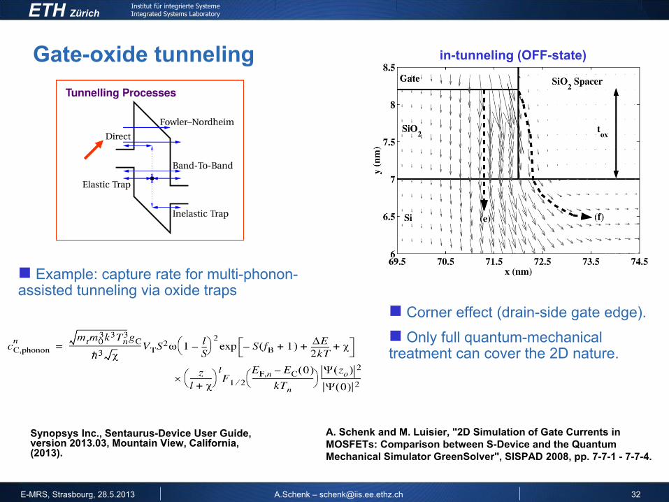
Gate-oxide tunneling in-tunneling (OFF-state)
Corner effect (drain-side gate edge).
Only full quantum-mechanical treatment can cover the 2D nature.
A. Schenk and M. Luisier, "2D Simulation of Gate Currents in
MOSFETs: Comparison between S-Device and the Quantum
Mechanical Simulator GreenSolver", SISPAD 2008, pp. 7-7-1 - 7-7-4.
Synopsys Inc., Sentaurus-Device User Guide, version 2013.03, Mountain View, California, (2013).
Example: capture rate for multi-phonon-assisted tunneling via oxide traps

Institut für integrierte Systeme Integrated Systems Laboratory ETH Zürich
E-MRS, Strasbourg, 28.5.2013
A.Schenk – [email protected]
33
USJ leakage simulation of
industrial samples
Institut für integrierte Systeme Integrated Systems Laboratory ETH Zürich
E-MRS, Strasbourg, 28.5.2013
A.Schenk – [email protected]
34
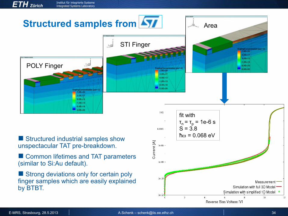
Area
STI Finger
POLY Finger
Structured samples from
fit with
τn = τp = 1e-6 s
S = 3.8
ħ = 0.068 eV Structured industrial samples show unspectacular TAT pre-breakdown.
Common lifetimes and TAT parameters (similar to Si:Au default).
Strong deviations only for certain poly finger samples which are easily explained by BTBT.
Institut für integrierte Systeme Integrated Systems Laboratory ETH Zürich
E-MRS, Strasbourg, 28.5.2013
A.Schenk – [email protected]
35
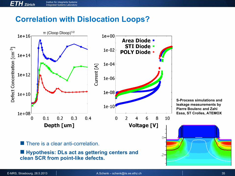
Correlation with Dislocation Loops?
There is a clear anti-correlation.
Hypothesis: DLs act as gettering centers and clean SCR from point-like defects.
S-Process simulations and
leakage measurements by
Pierre Boulenc and Zahi
Essa, ST Crolles, ATEMOX
π (Cloop Dloop)1/2
Related Documents