Proceedings of IMECE2006 2006 ASME International Mechanical Engineering Congress and Exposition November 5-10, 2006, Chicago, Illinois USA IMECE2006-13175 MODELING AND INPUT OPTIMIZATION UNDER UNCERTAINTY FOR A COLLECTION OF RF MEMS DEVICES M. S. Allen * J. E. Massad R. V. Field, Jr. Applied Mechanics Development, Org. 1526 Sandia National Laboratories 1 Albuquerque, New Mexico 87185 ABSTRACT The dynamic response of an RF MEMS device to a time- varying electrostatic force is optimized to enhance robustness to variations in material properties and geometry. The device func- tions as an electrical switch, where an applied voltage is used to close a circuit. The objective is to minimize the severity of the mechanical impact that occurs each time the switch closes, be- cause severe impacts have been found to significantly decrease the design life of these switches. The switch is modeled as a classical vibro-impact system: a single degree-of-freedom oscil- lator subject to mechanical impact with a single rigid barrier. Certain model parameters are described as random variables to represent the significant unit-to-unit variability observed during fabrication and testing of the collection of nominally-identical switches; these models for unit-to-unit variability are calibrated to available experimental data. Our objective is to design the shape and duration of the voltage waveform so that impact ve- locity at switch closure for the collection of nominally-identical switches is minimized subject to design constraints. The method- ology is also applied to search for design changes that reduce the impact velocity and to predict the effect of fabrication pro- cess improvements. INTRODUCTION Radio Frequency Micro Electro Mechanical System (RF MEMS) switches have been the subject of study for a number of applications because they can potentially provide very low power consumption, high isolation, and greater linearity at low cost and * Address all correspondence to this author. Email: [email protected]. 1 Sandia is a multiprogram laboratory operated by Sandia Corporation, a Lockheed Martin Company, for the United States Department of Energy’s Na- tional Nuclear Security Administration under Contract DE-AC04-94AL85000. in a compact package [1] [2] [3]. Unfortunately, current designs for RF switches fail to achieve the high reliability demanded for many applications. The high velocity with which the switches can impact the electrical contacts is one contributing factor. Re- cent research at Sandia has revealed that the actuating voltage pulse can be shaped to limit the velocity with which the plate im- pacts the electrical contacts, increasing a switch’s life by orders of magnitude. Unfortunately, there is considerable unit-to-unit variability in the dimensions and the properties of these switches, so a waveform designed to minimize the contact velocity, or pro- vide a soft landing, for the nominal switch is not effective for a batch of switches manufactured using current processes. This work demonstrates that the actuating voltage waveform can be optimized for a collection of RF switches with random physical parameters in order to minimize the contact velocity ex- perienced by the ensemble. This can be cast as a problem of optimization under uncertainty or Reliability-Based Design Op- timization (RBDO) [4]. The procedure is also used to optimize the design of the RF switches to reduce the contact velocity of the ensemble and to study the effect of reducing the degree of variation due to the manufacturing process. Reliability-Based Design Optimization has received consid- erable attention in recent years. A few researchers have applied RBDO to MEMS systems in order to improve the robustness of device designs, in part because MEMS systems tend to suffer from significant manufacturing variation and exhibit complex or uncertain physical phenomena. Optimization under uncertainty methodologies can be classified as Robust Design Optimization (RDO) methods or as Reliability- Based Design Optimization (RBDO) methods [4]. RDO methods use deterministic analysis to attempt to maximize deterministic performance while mini- mizing the sensitivity of the optimum design to uncertain or ran- dom parameters. For example, Han and Kwak [5] used this ap- 1 Copyright c 2006 by ASME

Welcome message from author
This document is posted to help you gain knowledge. Please leave a comment to let me know what you think about it! Share it to your friends and learn new things together.
Transcript
Proceedings of IMECE20062006 ASME International Mechanical Engineering Congress and Exposition
November 5-10, 2006, Chicago, Illinois USA
IMECE2006-13175
MODELING AND INPUT OPTIMIZATION UNDER UNCERTAINTY FOR ACOLLECTION OF RF MEMS DEVICES
M. S. Allen∗J. E. MassadR. V. Field, Jr.
Applied Mechanics Development, Org. 1526Sandia National Laboratories1
Albuquerque, New Mexico 87185
ABSTRACTThe dynamic response of an RF MEMS device to a time-
varying electrostatic force is optimized to enhance robustness tovariations in material properties and geometry. The device func-tions as an electrical switch, where an applied voltage is used toclose a circuit. The objective is to minimize the severity of themechanical impact that occurs each time the switch closes, be-cause severe impacts have been found to significantly decreasethe design life of these switches. The switch is modeled as aclassical vibro-impact system: a single degree-of-freedom oscil-lator subject to mechanical impact with a single rigid barrier.Certain model parameters are described as random variables torepresent the significant unit-to-unit variability observed duringfabrication and testing of the collection of nominally-identicalswitches; these models for unit-to-unit variability are calibratedto available experimental data. Our objective is to design theshape and duration of the voltage waveform so that impact ve-locity at switch closure for the collection of nominally-identicalswitches is minimized subject to design constraints. The method-ology is also applied to search for design changes that reducethe impact velocity and to predict the effect of fabrication pro-cess improvements.
INTRODUCTIONRadio Frequency Micro Electro Mechanical System (RF
MEMS) switches have been the subject of study for a number ofapplications because they can potentially provide very low powerconsumption, high isolation, and greater linearity at low cost and
∗Address all correspondence to this author. Email: [email protected] is a multiprogram laboratory operated by Sandia Corporation, a
Lockheed Martin Company, for the United States Department of Energy’s Na-tional Nuclear Security Administration under Contract DE-AC04-94AL85000.
in a compact package [1] [2] [3]. Unfortunately, current designsfor RF switches fail to achieve the high reliability demanded formany applications. The high velocity with which the switchescan impact the electrical contacts is one contributing factor. Re-cent research at Sandia has revealed that the actuating voltagepulse can be shaped to limit the velocity with which the plate im-pacts the electrical contacts, increasing a switch’s life by ordersof magnitude. Unfortunately, there is considerable unit-to-unitvariability in the dimensions and the properties of these switches,so a waveform designed to minimize the contact velocity, or pro-vide a soft landing, for the nominal switch is not effective for abatch of switches manufactured using current processes.
This work demonstrates that the actuating voltage waveformcan be optimized for a collection of RF switches with randomphysical parameters in order to minimize the contact velocity ex-perienced by the ensemble. This can be cast as a problem ofoptimization under uncertainty or Reliability-Based Design Op-timization (RBDO) [4]. The procedure is also used to optimizethe design of the RF switches to reduce the contact velocity ofthe ensemble and to study the effect of reducing the degree ofvariation due to the manufacturing process.
Reliability-Based Design Optimization has received consid-erable attention in recent years. A few researchers have appliedRBDO to MEMS systems in order to improve the robustness ofdevice designs, in part because MEMS systems tend to sufferfrom significant manufacturing variation and exhibit complex oruncertain physical phenomena. Optimization under uncertaintymethodologies can be classified as Robust Design Optimization(RDO) methods or as Reliability- Based Design Optimization(RBDO) methods [4]. RDO methods use deterministic analysisto attempt to maximize deterministic performance while mini-mizing the sensitivity of the optimum design to uncertain or ran-dom parameters. For example, Han and Kwak [5] used this ap-
1 Copyright c© 2006 by ASME
proach to optimize the design of a MEMS accelerometer and aresonant-type micro probe by augmenting their objective func-tion with the gradient of the objective function with respect tothe random parameters. Some limitations of RDO methods arethat they cannot provide information about the probability that adevice will fail and, because they are gradient based, they maynot perform properly if the objective function is noisy or highlynonlinear over the range spanned by the uncertain parameters.
RBDO methods are based on stochastic analysis and aretherefore preferred in many applications because they providean estimate of the reliability of a design and can more accuratelyaccount for variability in uncertain parameters. Heo, Yoon andKim used what may be classified as an RBDO method to op-timize the design of a MEMS thermal actuator [6]. Allen etal [7], presented an application of RBDO to a variable capac-itance MEMS capacitor. They validated the First-Order Relia-bility Method (FORM) for their application by comparing it toMonte Carlo Simulation (MCS) and then used FORM to opti-mize the design of the capacitor. FORM can be significantly lesscomputationally expensive than MCS, yet FORM may be inac-curate if the response is non-Gaussian or if the failure boundaryis not well approximated by a linear function. Allen et al ob-served that the FORM algorithm worked well even though theirsystem was nonlinear, yet all of the uncertain variables in theirsystem were assumed to be Gaussian with relatively small coef-ficients of variation. This assumption is often inappropriate forMEMS applications. Maute and Frangopol also used the FORMalgorithm as part of an optimization strategy for a MEMS de-vice [4]. One potential limitation of the FORM algorithm is thatit includes an iterative search cast as an optimization problem tofind the most probable point of failure. As a result, the FORMalgorithm becomes much more difficult to apply as the numberof uncertain parameters, and hence the dimension of this iterativeoptimization problem, increases. Also, because FORM is basedon optimization, one may encounter situations in which slow orlocal convergence is obtained, greatly increasing the complexityof implementing FORM and diminishing its computational effi-ciency. Neither Allen et al for Maute and Frangopol mentionedany difficulties obtaining convergence with the FORM algorithm,although their problems were limited to a small number of uncer-tain variables.
The work discussed here involves an objective function thatis highly nonlinear due to mechanical impact and whose uncer-tainties are large and highly non-Gaussian. For these reasons,Monte Carlo Simulation (MCS) was used to evaluate unit-to-unitvariability in these RF MEMS switches. Also, a low order math-ematical model exists that captures the physics of the device re-markably well, so the computational burden is low enough thatthe problem is tractable with MCS.
This paper is organized as follows. We first present a deriva-tion of a reduced order model that provides a good representationof the dynamics of the RF Switch to an actuating voltage. Theobjective function and optimization procedure are then discussedand some results presented. Finally, the effects of design and pro-cess improvement is illustrated followed by some conclusions.
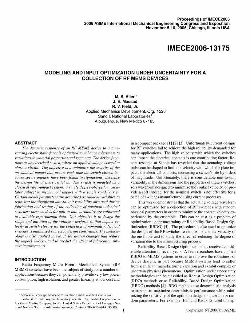
Figure 1. Schematic of RF MEMS switch.
MODEL DEFINITIONThe RF MEMS switch design of interest is shown in Fig. 1.
The switch consists of a stiff plate supported above a rigid sub-strate by four flexible supports. A 100 nm thick electrostatic padis adhered to the substrate below the switch plate to provide elec-trostatic actuation. When voltage is applied to the pad, the platedeflects downward and the contact tabs make mechanical contactwith the waveguide to close the circuit. Dyck et al described thedesign and characterization of this switch in [1].
A single degree-of-freedom model for the RF switch is usedfor analysis. Previous works have demonstrated the accuracyand utility of this model for these systems, especially whenthe input is shaped to limit excitation to higher frequencymodes [8] [9] [10]. Let X(t) denote the displacement of thecontact tabs; the equations of motion are
M X(t)+K X(t) =εa2
[u(t)
G−X(t)
]2
, X(0) = X(0) = 0, (1)
where M and K denote the effective mass and stiffness of theswitch plate, respectively. The right hand side of Eq. (1) definesthe applied electrostatic force, where ε and a denote the electricpermittivity of air and the surface area of the switch plate,respectively, G is the gap distance between the switch plate andelectrostatic pad at X = 0, and u(t) is the voltage waveformapplied to the pad. Mechanical impact between the contacttabs and waveguide is included by introducing the followingkinematic constraint
X(t+) =
{X(t−) if X(t−) < D,
−η X(t−) if X(t−) = D,(2)
where D denotes the travel distance for switch closure, andη ∈ (0,1] is the (deterministic) coefficient of restitution. A simi-lar model has been used to study the dynamic response of a col-lection of MEMS inertial switches [11]. Our convention is todenote all deterministic quantities with lower-case letters or sym-bols and all random quantities with upper-case letters or symbols.
MODEL CALIBRATIONGiven a small set of experimentally observed quantities, we
need to calibrate the model defined by Eqs. (1) and (2). Many ofthe parameters in Eqs. (1) and (2) cannot be measured directly,
2 Copyright c© 2006 by ASME
80 85 90 95 100 105
E (GPa)
PD
F
80 85 90 95 100 1050
1
2
3
Cou
nt
(a)
3.4 3.6 3.8 4 4.2
G (µm)
PD
F
3.4 3.6 3.8 4 4.20
1
2
Cou
nt
(b)
6 6.5 7 7.5 8
T (µm)
PD
F
6 6.5 7 7.5 80
1
2C
ount
(c)
2 2.5 3
D (µm)
PD
F
2 2.5 30
1
2
Cou
nt
(d)
3 3.5 4
x 10−9M (kg)
PD
F e
st
3 3.5 4
x 10−9
(e)
20 40 60 80 100
K (N/m)
PD
F e
st
20 40 60 80 100
(f)
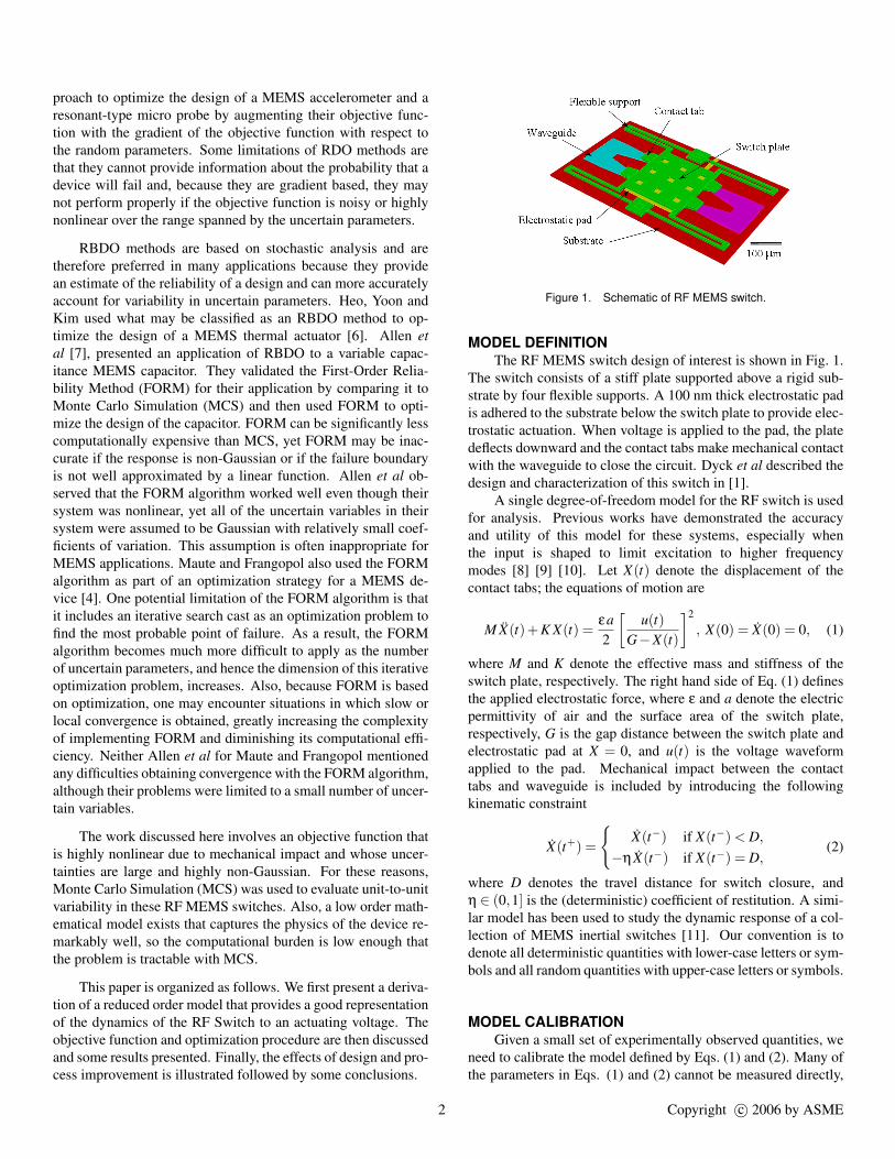
Figure 2. Models and available data for: (a) elastic modulus of plate,(b) electrostatic gap, (c) plate thickness, and (d) travel distance. One thou-sand sample histogram and PDF estimate of resulting correlated variables(e) effective mass and (f) effective stiffness.
so some effort was required to obtain them from the measureddata. The following experimentally observable quantities have asignificant effect on the switch model, and have been found to ex-hibit significant variability: modulus (E), gap (G), thickness (T )and travel distance (D). The data is shown in Figure 2 (a)-(d).(The modulus is actually not directly measurable, yet it can bededuced from the pull in voltage Upi as will be explained.) Themodel calibration procedure consists of first estimating proba-bilistic models of E, G, T , and D and then relating these quanti-ties to the parameters of Eqs. (1) and (2).
Expert opinion and past experience with the manufactur-ing process have found that G and D tend to be skewed to theright. A Beta distribution was fit to the available data for G andD because its parameters can be chosen so that it describes aslightly skewed, yet bounded distribution. Limited informationwas available for E and T , so these were taken to be uniformlydistributed in the interval bounded by ±25% of their nominalvalues.
These random variables must now be related to the modelparameters in Eqs. (1) and (2). The quasi-static voltage atwhich the switch closes, dubbed the ”pull-in voltage” Upi can berelated to the model parameters as follows. The system in Eq. (1)exhibits a snapping phenomenon, in which the effective stiffnessof the switch becomes negative for sufficiently large voltageU . The snap through point, found by solving for the positionof the switch at which the stiffness changes sign is X = G/3.
Substituting this position for X in Eq. (1) and neglecting inertiasince the pull in tests are performed quasi-statically, one obtainsteh following expression for Upi.
Upi =
√827
K G3
εa. (3)
A three dimensional static finite element analysis was used tofind the effective stiffness of the switch for various values of theswitch thicknesses. The following polynomial relationship be-tween the effective stiffness of the switch and its thickness andmodulus was then fit to the FEA results for thickness rangingfrom 5µm to 9µm.
K (E,T ) = a2 E T (T −a1) (4)
where E is the Young’s modulus, T is the switch thickness, anda1 = 3.1458 and a2 = 0.027186 are the coefficients of the poly-nomial fit. Equation (4) can be substituted into (3) to solve forthe modulus in terms of Upi, T , and G. The four parametersdefining the switch, D, G, T and E are assumed to be indepen-dent, while it is noted that the procedure for determining E couldlead to artificial correlation between them if the measurements orstatic Finite Element model contain large errors.
The thickness and modulus of the switches both determinethe effective stiffness of the single degree of freedom modelthrough Eq. (4). The effective mass is found using the follow-ing procedure. A dynamic finite element model was used to de-termine the following relationship between the natural frequencyof the switch plate bounce mode fb and the plate thickness andmodulus
fb =√
E b1 (T +b0) (5)
where the coefficients b0 = 0.43613 and b1 = 311.79 are validover the same range as a1 and a2. Assuming that the static stiff-ness K is approximately equal to the dynamic stiffness of the sys-tem oscillating in its bounce mode only, the effective mass canbe found using the familiar relationship f = 2π
√K/M yielding
M =K
(2π fb)2 . (6)
This procedure was verified by solving for both the stiffness andmass using the mode shape and natural frequency of the bouncemode and comparing them to the values obtained by the proce-dure described previously. The stiffness and mass values foundusing each method were found to agree to within a few percent.
The effective mass is actually a function of the thicknessonly, as can be seen by substituting the polynomials in Eqs. (4)and (5) into Eq. (6) resulting in
M =a2 T (T −a1)
(2πb1 (T +b0))2 . (7)
3 Copyright c© 2006 by ASME

Histograms of M and K, generated from 1000 samples of theindependent random variables D, G, T and E, are shown in Fig. 2(e) and (f) respectively. Note that, by Eq. (6) and (4), M and Kare dependent random variables. Samples of D, G, K and M areused to perform Monte Carlo simulations of Eqs. (1) and (2). Thecoefficient of restitution is taken to be η = 0.5, which was foundto adequately describe the rebound of an elastic 3D finite elementmodel of the switch that included contact.
PERFORMANCE METRICSThe objective of waveform optimization is to maximize the
life of the RF switches while maintaining acceptable time toclosure. Previous investigations have found that switch life in-creases by a few orders of magnitude when the voltage wave-form is designed to minimize the velocity with which a switchimpacts the electrical contacts. The present study is concernedwith minimizing the contact velocity for an ensemble of switcheswith random parameters. The maximum contact velocity V for agiven switch is defined as the maximum velocity X at the instantst−k just before the switch rebounds from the contacts,
V = max∣∣X (
t−k)∣∣ . (8)
The contact velocity for the ensemble was minimized by mini-mizing the velocity vu of the switch at the 10% upper quantiledefined as
P(V > vu) = 0.1. (9)
The velocity vu represents the worst case impact velocity for 90%of the ensemble and will be referred to as the upper velocitythroughout this work. The upper velocity is estimated by as
vu = F−1 (0.9) (10)
where F is an approximation for the cumulative distributionfunction of V [12]. An optimum waveform must also assure thatthe probability of a switch remaining unclosed pnc for a largetime is small This was estimated as the ratio of the number ofswitches that did not close within 250µs to the total number ofswitches in the MCS. The following objective function accountsfor both of these considerations and was used in the followingsection to optimize the voltage waveform.
g = vu + c1 pnc (11)
The relative importance of contact velocity and failure to close isspecified by the constant c1. A value of c1 = 0.0025 was used inthis study for upper velocities in cm/s.
OPTIMIZATION PROCEDUREA computational routine was created to solve the equation
of motion, Eq. (1), subject to the constraint in Eq. (2) using an
0 10 20 30 400
50
100
150
200
time (µs)
Vo
ltag
e (V
olt
s)
ts(1)
tr(1)
tp(1)
u1
ts(2)
u2
tr(2)
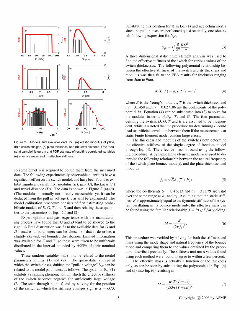
Figure 3. Sample actuation voltage waveform and parameter definitions.
adaptive Runge-Kutta time integration routine (Matlab’s ode45).The equation of motion was solved for 200 independent realiza-tions of the random variables D, G, K and M sampled from thedistributions described previously. The upper velocity vu and theprobability of a switch not closing Pnc were estimated for eachMonte Carlo simulation, yielding a single value for the objectivefunction g for each Monte Carlo simulation via Eq. (11). TheMonte Carlo simulation was repeated for various voltage wave-forms in order to arrive at an optimum voltage waveform.
The voltage waveform was parameterized by sets of four pa-rameters per pulse in order to simplify the optimization proce-dure. These parameters are illustrated in Fig. 3 for a two-pulsewaveform. Pulse i is parameterized by its start time t(i)s , rise timet(i)r , peak time t(i)p and peak voltage ui. The fall time of eachpulse is identical to its rise time. This is a generalization of thepulse/coast waveform used in [8].
Initially, we restrict the analysis to waveforms with twopulses. The optimization procedure was simplified by first con-sidering each pulse independently. The purpose of the first pulseis to bring the ensemble of switches near to the closed positionwith minimal velocity. Because of the nonlinear dependence ofthe force applied to the oscillator on (G−X(t))−2, one wouldexpect that longer forces will tend to increase the width of thedistribution of the ensemble displacement and velocity. For thisreason, the voltage of the first pulse was set at u1 = 150 volts,which is near the maximum allowable voltage, so its width couldbe minimum while imparting the necessary amount of energy tothe switch. The rise time for this pulse was set at t(1)
r = 4µs,which was found previously to be the fastest rise time that couldbe used without exciting higher modes of the switch. The widthof this pulse was increased from zero with the other parametersfor this pulse fixed and with the second pulse nullified until apulse width was found that resulted in a maximum contact ve-locity of about 10cm/s over the ensemble of switches.
Once the peak time of the first pulse had been determined,Monte Carlo analysis was performed for various values of t(2)
s ,t(2)r and u2, typically four values of t(2)
s and three values each ofthe other two. The set of parameters that minimized the costfunction were then used as starting values for a Nelder-Mead
4 Copyright c© 2006 by ASME
simplex algorithm (Matlab’s ’fminsearch’) [13]. This algorithmvaried the values for t(1)
p , t(2)s , t(2)
r and u2 until the objective func-tion defined by Eq. (11) was minimized. This typically entailed100-200 runs of the Monte Carlo simulation and improved themean and upper contact velocities by about 1−2cm/s comparedto the starting values.
The DIRECT algorithm in [14] was also applied to this prob-lem in an effort to perform the optimization in a single step, yetit was abandoned when it failed to obtain the optimum inputwaveform after 350 evaluations of the Monte Carlo simulation.However, the DIRECT algorithm was helpful in finding optimumparameters for a three pulse waveform, because there were toomany unknown parameters to use the simple optimization proce-dure described previously. Unfortunately, the three pulse wave-form did not significantly reduce the contact velocity relative tothe two-pulse waveform, and it was significantly more difficultto optimize its parameters, so it was abandoned.
RESULTSThe contact velocity for the ensemble of switches described
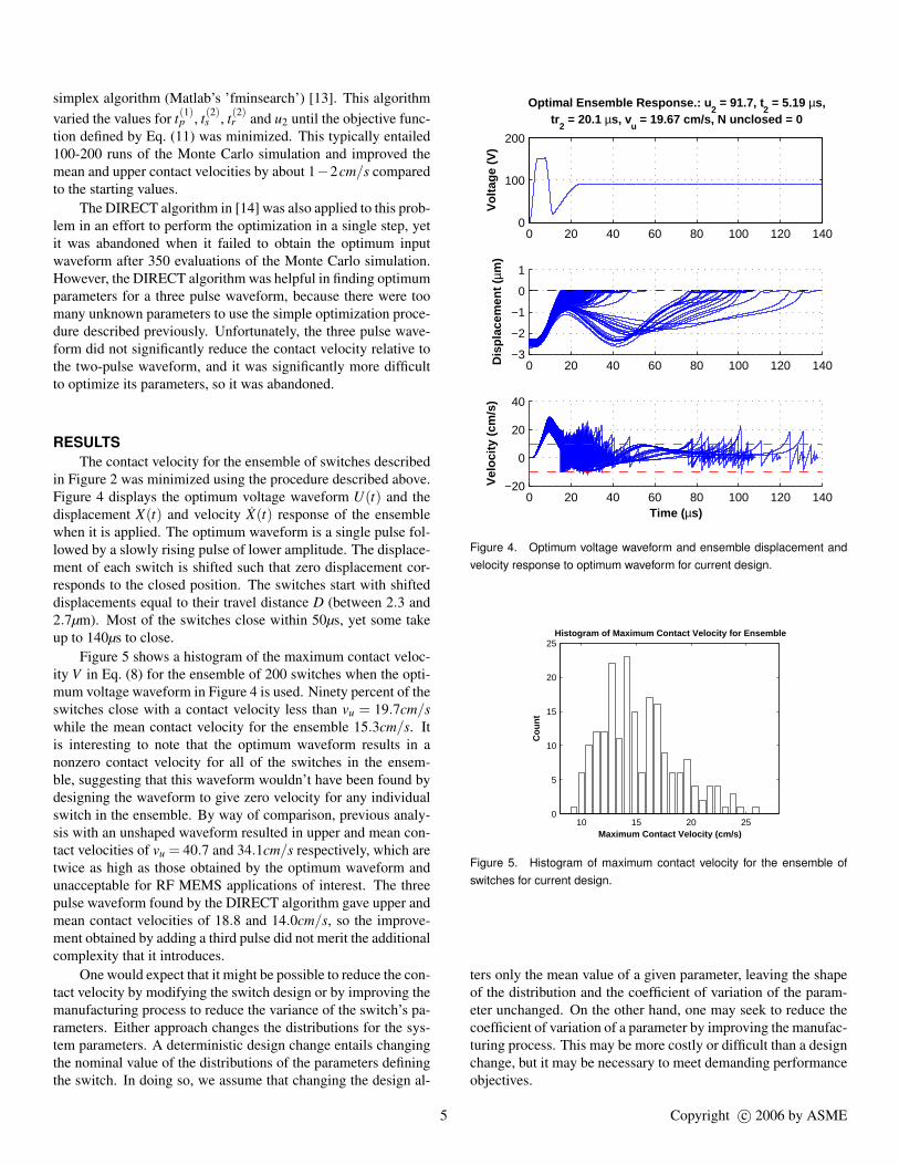
in Figure 2 was minimized using the procedure described above.Figure 4 displays the optimum voltage waveform U(t) and thedisplacement X(t) and velocity X(t) response of the ensemblewhen it is applied. The optimum waveform is a single pulse fol-lowed by a slowly rising pulse of lower amplitude. The displace-ment of each switch is shifted such that zero displacement cor-responds to the closed position. The switches start with shifteddisplacements equal to their travel distance D (between 2.3 and2.7µm). Most of the switches close within 50µs, yet some takeup to 140µs to close.
Figure 5 shows a histogram of the maximum contact veloc-ity V in Eq. (8) for the ensemble of 200 switches when the opti-mum voltage waveform in Figure 4 is used. Ninety percent of theswitches close with a contact velocity less than vu = 19.7cm/swhile the mean contact velocity for the ensemble 15.3cm/s. Itis interesting to note that the optimum waveform results in anonzero contact velocity for all of the switches in the ensem-ble, suggesting that this waveform wouldn’t have been found bydesigning the waveform to give zero velocity for any individualswitch in the ensemble. By way of comparison, previous analy-sis with an unshaped waveform resulted in upper and mean con-tact velocities of vu = 40.7 and 34.1cm/s respectively, which aretwice as high as those obtained by the optimum waveform andunacceptable for RF MEMS applications of interest. The threepulse waveform found by the DIRECT algorithm gave upper andmean contact velocities of 18.8 and 14.0cm/s, so the improve-ment obtained by adding a third pulse did not merit the additionalcomplexity that it introduces.
One would expect that it might be possible to reduce the con-tact velocity by modifying the switch design or by improving themanufacturing process to reduce the variance of the switch’s pa-rameters. Either approach changes the distributions for the sys-tem parameters. A deterministic design change entails changingthe nominal value of the distributions of the parameters definingthe switch. In doing so, we assume that changing the design al-
0 20 40 60 80 100 120 1400
100
200
Vo
ltag
e (V
)
Optimal Ensemble Response.: u2 = 91.7, t
2 = 5.19 µs,
tr2 = 20.1 µs, v
u = 19.67 cm/s, N unclosed = 0
0 20 40 60 80 100 120 140−3
−2
−1
0
1
Dis
pla
cem
ent
(µm
)0 20 40 60 80 100 120 140
−20
0
20
40
Time (µs)
Vel
oci
ty (
cm/s
)
Figure 4. Optimum voltage waveform and ensemble displacement andvelocity response to optimum waveform for current design.
10 15 20 250
5
10
15
20
25
Maximum Contact Velocity (cm/s)
Co
un
t
Histogram of Maximum Contact Velocity for Ensemble
Figure 5. Histogram of maximum contact velocity for the ensemble ofswitches for current design.
ters only the mean value of a given parameter, leaving the shapeof the distribution and the coefficient of variation of the param-eter unchanged. On the other hand, one may seek to reduce thecoefficient of variation of a parameter by improving the manufac-turing process. This may be more costly or difficult than a designchange, but it may be necessary to meet demanding performanceobjectives.
5 Copyright c© 2006 by ASME
Design ChangesThe optimization methodology was also applied to study the
effect of design changes on switch contact velocity. Determin-istic analysis of Eq. (1) reveals that the system has an unstableequilibrium at X = G/3. With the current design, most of theswitches close between 0.59 ≤ D/G ≤ 0.75. The design wasmodified to reduce this ratio (resulting in 0.41≤D/G≤ 0.52 forthe new design) and a new optimum waveform was found forthe modified design. The modified design is described by a newcollection of random variables D′, G′, K′ and M′, whose meanvalues have been altered. The new random variables are obtainedfrom the old such that the coefficient of variation of each remainsunchanged, i.e.
Y ′ =(
1+∆µµ
)Y, (12)
where Y ′ is the distribution whose mean value µ has shifted by∆µ. In order to preserve a feasible design, the values of D andG were increased and decreased respectively by only 0.5µm, andthe mean value of the distribution that defines the thickness ofthe switches was increased by 0.6µm. Samples of D′, G′, T ′ andE ′ were used to generate correlated samples for K′ and M′.
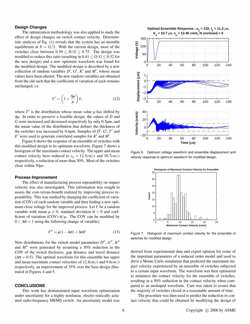
Figure 6 shows the response of an ensemble of switches withthis modified design to its optimum waveform. Figure 7 shows ahistogram of the maximum contact velocity. The upper and meancontact velocity have reduced to vu = 12.5cm/s and 10.7cm/srespectively, a reduction of more than 30%. Most of the switchesclose within 50µs.
Process ImprovementThe effect of manufacturing process repeatability on impact
velocity was also investigated. This information was sought toassess the cost-versus-benefit realized by improving process re-peatability. This was studied by changing the coefficient of varia-tion (COV) of each random variable and then finding a new opti-mum close voltage for the improved process. Let Y be a randomvariable with mean µ 6= 0, standard deviation σ > 0 and coef-ficient of variation (COV) σ/µ. The COV can be modified by0 < ∆σ < 1 using the following change of variables:
Y ′′ = µ(1−∆σ)+∆σY (13)
New distributions for the switch model parameters D′′, G′′, K′′
and M′′ were generated by assuming a 50% reduction in theCOV of the switch thickness, gap distance and travel distance(∆σ = 0.5). The optimal waveform for this ensemble has upperand mean maximum contact velocities of 12.8cm/s and 9.6cm/srespectively, an improvement of 35% over the base design illus-trated in Figures 4 and 5.
CONCLUSIONSThis work has demonstrated input waveform optimization
under uncertainty for a highly nonlinear, electro-statically actu-ated radio-frequency MEMS switch. An uncertainty model was
0 20 40 60 80 100 120 1400
50
100
150
Vo
ltag
e (V
)
Optimal Ensemble Response.: u2 = 132, t
2 = 11.3 µs,
tr2 = 10.7 µs, v
u = 12.46 cm/s, N unclosed = 0
0 20 40 60 80 100 120 140−3
−2
−1
0
1
Dis
pla
cem
ent
(µm
)0 20 40 60 80 100 120 140
−20
0
20
40
Time (µs)
Vel
oci
ty (
cm/s
)
Figure 6. Optimum voltage waveform and ensemble displacement andvelocity response to optimum waveform for modified design.
0 5 10 15 20 250
5
10
15
20
25
30
35
Maximum Contact Velocity (cm/s)
Co
un
t
Histogram of Maximum Contact Velocity for Ensemble
Figure 7. Histogram of maximum contact velocity for the ensemble ofswitches for modified design.
derived from experimental data and expert opinion for some ofthe important parameters of a reduced order model and used todrive a Monte Carlo simulation that predicted the maximum im-pact velocity experienced by an ensemble of switches subjectedto a certain input waveform. The waveform was then optimizedto minimize the contact velocity for the ensemble of switches,resulting in a 50% reduction in the contact velocity when com-pared to an unshaped waveform. Care was taken to assure thatthe majority of switches closed in a reasonable amount of time.
The procedure was then used to predict the reduction in con-tact velocity that could be obtained by modifying the design of
6 Copyright c© 2006 by ASME

the switch, and one design was presented that reduced the contactvelocity by 30%. Other modifications of this class are currentlybeing investigated considering all of the manufacturing and elec-trical performance constraints on the switches. Finally, the pro-cedure was used to predict the effect of improving the processon the contact velocity, revealing that a 50% reduction in thecoefficient of variation of the process resulted in a 35% in thecontact velocity of the ensemble of switches. This information isvaluable when performing cost-benefit analyses to justify futureinvestments to improve the fabrication process and to allocateproject resources between design and process improvement.
ACKNOWLEDGEMENTSThe authors gratefully acknowledge the technical contribu-
tions of Christopher W. Dyck and William D. Cowan in thiswork.
REFERENCES[1] Dyck, C., Plut, T. A., Nordquist, C. D., Finnegan, P. S.,
Austin, F., and Reines, I., 2004. “Fabrication and char-acterization of ohmic contacting rf mems switches”. InSPIE Conference on Micromachining and Microfabrica-tion, Vol. 5344, pp. 79–88.
[2] Marchetti, B., Cannella, F., Caso, T., and Margesin, B.,2006. “Experimental numerical dynamic characterizationof series rf mems”. In 24th International Modal AnalysisConference (IMAC XXIV).
[3] Yao, J., 2000. “Rf mems from a device perspective”. J.Micromech. Microeng., 10, pp. R9–R38.
[4] Maute, K., and Frangopol, D. M., 2003. “Reliability-baseddesign of mems mechanisms by topology optimization”.Computers and Structures, 81, pp. 813–824.
[5] Han, J. S., and Kwak, B. M., 2004. “Robust optimizationusing a gradient index: Mems applications”. Struct Multi-disc Optim, 27, pp. 469–478.
[6] Heo, S., Yoon, G. H., and Kim, Y. Y., 2004. “The ro-bust design for micro electro-thermal actuators”. In SmartStructures and Materials 2004: Smart Electronics, MEMS,BioMEMS, and Nanotechnology, V. K. Varadan, ed., Pro-ceedings of SPIE Vol. 5389.
[7] Allen, M., Raullin, M., Maute, K., and Frangopol, D. M.,2004. “Reliability-based analysis and design optimizationof electrostatically actuated mems”. Computers and Struc-tures, 82, pp. 1007–1020.
[8] Czaplewski, D., Dyck, C., Sumali, H., Massad, J., Kup-pers, J., Reines, I., Cowan, W., and Tigges, C., 2006. “Asoft landing waveform for actuation of a single pole sin-gle throw ohmic rf mems switch”. Journal of Micromech.Microeng.(accepted).
[9] Sumali, H., Kuppers, J., Czaplewski, D., Massad, J., andDyck, C., 2005. “Structural dynamics of an rf memsswitch”. In 2005 ASME International Mechanical Engi-neering Congress and Exposition (IMECE).
[10] Massad, J., Sumali, H., Epp, D. S., and Dyck, C., 2005.“Modeling, simulation, and testing of the mechanical dy-
namics of an rf mems switch”. In Proceedings of the 2005International Conference on MEMS, NANO and SmartSystems (ICMENS05), pp. 237–240.
[11] Field, Jr., R., and Reese, S., 2005. “Probabilistic analysisand design of a MEMS deceleration switch”. In Proceed-ings of the 2005 ASME International Mechanical Engineer-ing Conference.
[12] Ang, A., and Tang, W., 1975. Probability Concepts in En-gineering Planning and Design: Vol. 1 - Basic Principles.John Wiley and Sons, Inc., New York, NY.
[13] Lagarias, J. C., Reeds, J. A., Wright, M. H., and Wright,P. E., 1998. “Convergence properties of the nelder-meadsimplex method in low dimensions”. SIAM J. OPTIM.,9(1), pp. 112–147.
[14] Perttunen, C., Jones, D., and Stuckman., B., 1993. “Lip-schitzian optimization without the lipschitz constant”.Journal of Optimization Theory and Application, 79(1),pp. 157–181.
NOTE: M. Allen in [7] is not the primary author of this work
7 Copyright c© 2006 by ASME
Related Documents


