SERVICE MANUAL CD PLAYER MODEL DCD-500AE TOKYO, JAPAN Denon Brand Company, D&M Holdings Inc. Some illustrations using in this service manual are slightly different from the actual set. ● Please use this service manual with referring to the operating instructions without fail. ● For purposes of improvement, specifications and design are subject to change without notice. ● ● 本文中に使用しているイラストは、説明の都合上現物 と多少異なる場合があります。 ● 修理の際は、必ず取扱説明書を参照の上、作業を行っ てください。 サービスをおこなう前に、このサービスマニュアルを 必ずお読みください。本機は、火災、感電、けがなど に対する安全性を確保するために、さまざまな配慮を おこなっており、また法的には「電気用品安全法」に もとづき、所定の許可を得て製造されております。 従ってサービスをおこなう際は、これらの安全性が維 持されるよう、このサービスマニュアルに記載されて いる注意事項を必ずお守りください。 ● 本機の仕様は性能改良のため、予告なく変更すること があります。 ● 補修用性能部品の保有期間は、製造打切後8年です。 注 意 X0303 V.01 DE/CDM 0608 For Europe & Taiwan R.O.C. model Ver. 1

Welcome message from author
This document is posted to help you gain knowledge. Please leave a comment to let me know what you think about it! Share it to your friends and learn new things together.
Transcript
SERVICE MANUAL
CD PLAYER
MODEL DCD-500AE
TOKYO, JAPAN
Denon Brand Company, D&M Holdings Inc.
Some illustrations using in this service manual are
slightly different from the actual set.
●
Please use this service manual with referring to the
operating instructions without fail.
●
For purposes of improvement, specifications and
design are subject to change without notice.
●
● 本文中に使用しているイラストは、説明の都合上現物 と多少異なる場合があります。
● 修理の際は、必ず取扱説明書を参照の上、作業を行っ てください。
サービスをおこなう前に、このサービスマニュアルを必ずお読みください。本機は、火災、感電、けがなどに対する安全性を確保するために、さまざまな配慮をおこなっており、また法的には「電気用品安全法」にもとづき、所定の許可を得て製造されております。従ってサービスをおこなう際は、これらの安全性が維持されるよう、このサービスマニュアルに記載されている注意事項を必ずお守りください。
● 本機の仕様は性能改良のため、予告なく変更すること があります。● 補修用性能部品の保有期間は、製造打切後8年です。
注 意
X0303 V.01 DE/CDM 0608
For Europe &
Taiwan R.O.C. model
Ver. 1
2
DCD-500AE
Please heed the points listed below during servicing and inspection.
◎Heed the cautions!Spots requiring particular attention when servicing, such asthe cabinet, parts, chassis, etc., have cautions indicated onlabels or seals. Be sure to heed these cautions and the cau-tions indicated in the handling instructions.
◎Caution concerning electric shock!(1) An AC voltage is impressed on this set, so touching inter-
nal metal parts when the set is energized could causeelectric shock. Take care to avoid electric shock, by for ex-ample using an isolating transformer and gloves whenservicing while the set is energized, unplugging the powercord when replacing parts, etc.
(2)There are high voltage parts inside. Handle with extra carewhen the set is energized.
◎Caution concerning disassembly and assembly!Though great care is taken when manufacturing parts fromsheet metal, there may in some rare cases be burrs on theedges of parts which could cause injury if fingers are movedacross them. Use gloves to protect your hands.
◎Only use designated parts!The set's parts have specific safety properties (fire resis-tance, voltage resistance, etc.). For replacement parts, besure to use parts which have the same properties. In particu-lar, for the important safety parts that are marked ! on wiringdiagrams and parts lists, be sure to use the designated parts.
◎Be sure to mount parts and arrange thewires as they were originally!
For safety reasons, some parts use tape, tubes or other insu-lating materials, and some parts are mounted away from thesurface of printed circuit boards. Care is also taken with thepositions of the wires inside and clamps are used to keepwires away from heating and high voltage parts, so be sure toset everything back as it was originally.
◎ Inspect for safety after servicing!Check that all screws, parts and wires removed or discon-nected for servicing have been put back in their original posi-tions, inspect that no parts around the area that has beenserviced have been negatively affected, conduct an insulationcheck on the external metal connectors and between theblades of the power plug, and otherwise check that safety isensured.
(Insulation check procedure)Unplug the power cord from the power outlet, disconnect theantenna, plugs, etc., and turn the power switch on. Using a500V insulation resistance tester, check that the insulation re-sistance between the terminals of the power plug and the ex-ternally exposed metal parts (antenna terminal, headphonesterminal, microphone terminal, input terminal, etc.) is 1MΩ orgreater. If it is less, the set must be inspected and repaired.
Concerning important safety parts
Many of the electric and structural parts used in the set havespecial safety properties. In most cases these properties aredifficult to distinguish by sight, and using replacement partswith higher ratings (rated power and withstand voltage) doesnot necessarily guarantee that safety performance will be pre-served. Parts with safety properties are indicated as shownbelow on the wiring diagrams and parts lists is this servicemanual. Be sure to replace them with parts with the designat-ed part number.
(1) Schematic diagrams ... Indicated by the ! mark.
(2) Parts lists ... Indicated by the ! mark.
Using parts other than the designated partscould result in electric shock, fires or otherdangerous situations.
SAFETY PRECAUTIONSThe following check should be performed for the continued protection of the customer and service technician.
LEAKAGE CURRENT CHECKBefore returning the unit to the customer, make sure you make either (1) a leakage current check or (2) a line to chassisresistance check. If the leakage current exceeds 0.5 milliamps, or if the resistance from chassis to either side of the powercord is less than 460 kohms, the unit is defective.
LASER RADIATIONDo not stare into beam or view directly with optical instruments, class 3A laser product.
CAUTION
CAUTION
サービス、点検時にはつぎのことにご注意願います。
◎注意事項をお守りください!サービスのとき特に注意を必要とする個所についてはキャビネット、部品、シャーシなどにラベルや捺印で注意事項を表示しています。これらの注意書きおよび取扱説明書などの注意事項を必ずお守りください。
◎感電に注意!(1) このセットは、交流電圧が印加されていますので通電時に内部金属部に触れると感電することがあります。従って通電サービス時には、絶縁トランスの使用や手袋の着用、部品交換には、電源プラグを抜くなどして感電にご注意ください。
(2) 内部には高電圧の部分がありますので、通電時の取扱には十分ご注意ください。
◎分解、組み立て作業時のご注意!板金部品の端面の『バリ』は、部品製造時に充分管理をしておりますが、板金端面は鋭利となっている箇所が有りますので、部品端面に触れたまま指を動かすとまれに怪我をする場合がありますので十分注意して作業して下さい。手の保護のために手袋を着用してください。
◎指定部品の使用!セットの部品は難燃性や耐電圧など安全上の特性を持ったものとなっています。従って交換部品は、使用されていたものと同じ特性の部品を使用してください。特に配線図、部品表に ! 印で指定されている安全上重要な部品は必ず指定のものをご使用ください。
◎部品の取付けや配線の引きまわしは、 元どおりに!安全上、テープやチューブなどの絶縁材料を使用したり、プリント基板から浮かして取付けた部品があります。また内部配線は引きまわしやクランパーによって発熱部品や高圧部品に接近しないように配慮されていますので、これらは必ず元どおりにしてください。
◎サービス後は安全点検を!サービスのために取り外したねじ、部品、配線などが元どおりになっているか、またサービスした個所の周辺を劣化させてしまったところがないかなどを点検し、外部金属端子部と、電源プラグの刃の間の絶縁チェックをおこなうなど、安全性が確保されていることを確認してください。
(絶縁チェックの方法)電源コンセントから電源プラグを抜き、アンテナやプラグなどを外し、電源スイッチを入れます。500V 絶縁抵抗計を用いて、電源プラグのそれぞれの端子と外部露出金属部[アンテナ端子、ヘッドホン端子マイク端子、入力端子など]との間で、絶縁抵抗値が1 MΩ 以上であること、この値以下のときはセットの点検修理が必要です。
安全上重要な部品について
本機に使用している多くの電気部品、および機構部品は安全上、特別な特性を持っています。この特性はほとんどの場合、外観では判別つきにくく、またもとの部品より高い定格(定格電力、耐圧)を持ったものを使用しても安全性が維持されるとは、限りません。安全上の特性を持った部品は、このサービスマニュアルの配線図、部品表につぎのように表示していますので必ず指定されている部品番号のものを使用願います。
(1) 配線図… ! マークで表示しています。
(2) 部品表… ! マークで表示しています。
指定された部品と異なるものを使用した場合には、感電、火災などの危険を生じる恐れがあります。
注 意
注 意
3
DCD-500AE
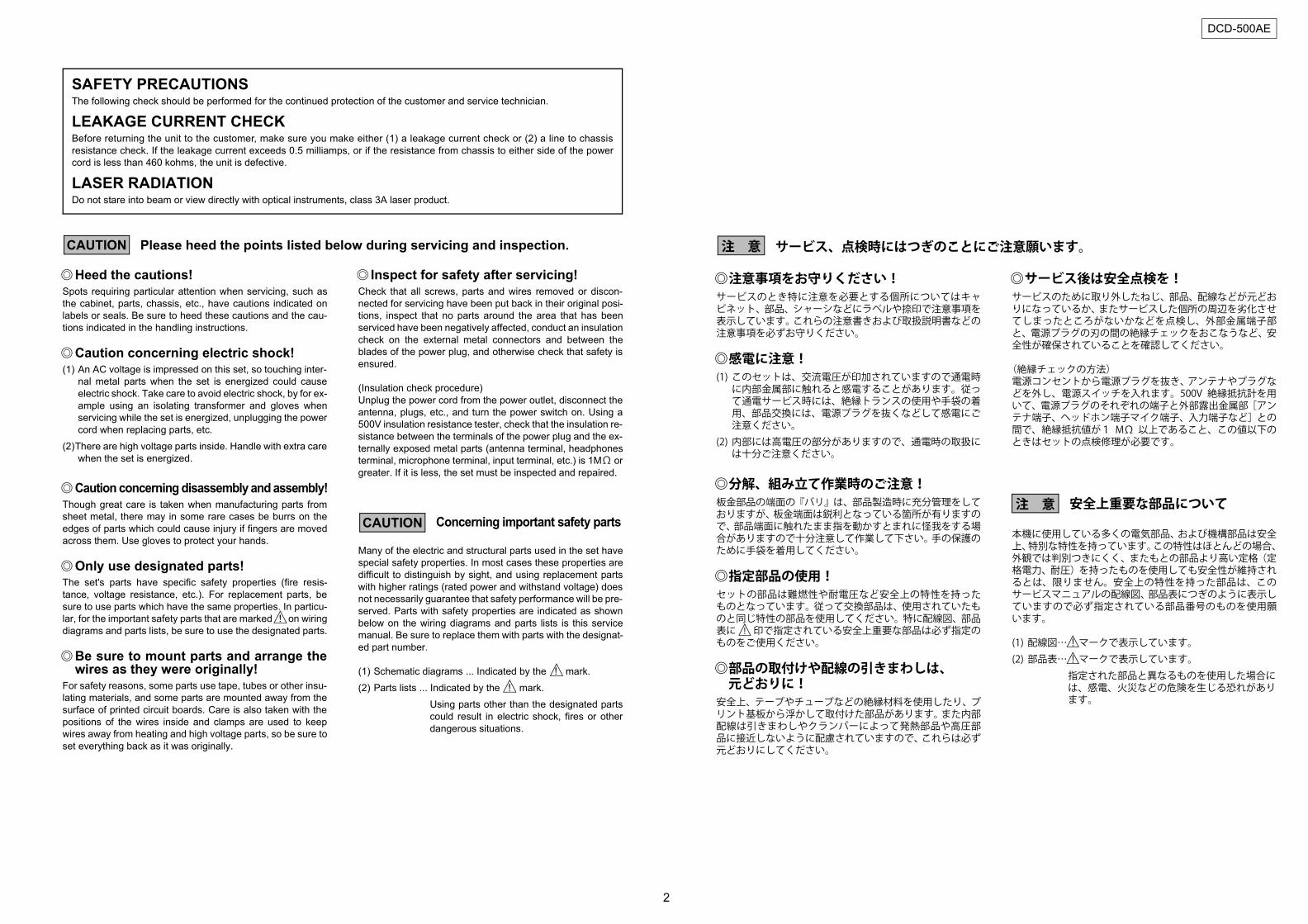
各部のはずしかた(組み立てるときは、逆の順序でおこなってください。)
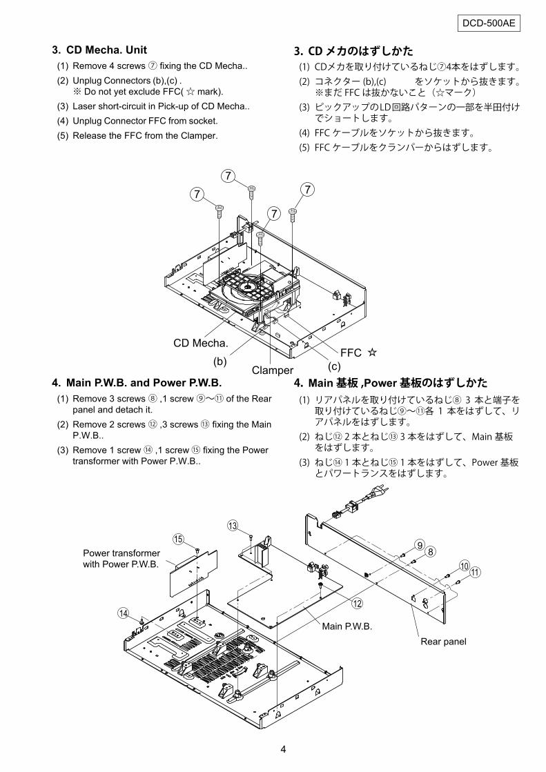
1. トップカバーのはずしかた(1) 側面のねじ① 4本をはずします。
(2) 後面のねじ② 5本をはずします。
(3) トップカバーを矢印の方向へはずします。
2. フロントパネルのはずしかた(1) ねじ③ 2 本をはずしチャッキングプレートをはずします。ドライブギア(a)を時計回りに廻して CD トレイを引き出して、ローダーパネルをはずします。
(2) リングワイヤーを止めているねじ④1本をはずします。
(3) フロントパネル底部のねじ⑤ 4本をはずします。
(4) フロントパネル左右側部のねじ⑥ 2本をはずします。
(5) フロントパネルをはずします。
( 注)まだ FFC( ☆マーク ) は抜かないこと。
DISASSEMBLY(Follow the procedure below in reverse order when reassem-bling.)
1. Top Cover(1) Remove 4 screws ① on both sides.
(2) Remove 5 screws ② on rear side.
(3) Detach the Top cover as shown in the fig.
2. Front Panel(1) Take off the Chucking plate after removing 2 screws③ .
Open the CD tray by turning the Drive gear (a) clockwise, then detach the Loader panel.
(2) Remove 1 screw ④ fixing the Ring wire.(3) Remove 4 screws ⑤on the bottom edge of the Front pan-
el.
(4) Remove 2 screws ⑥ , at L/R ends of the Front panel.
(5) Detach the Front panel.
Note : Do not yet exclude FFC(☆ mark).
Top cover
CD tray
(a)Drive gear
Ring wire
Loader panel
Chucking plate
Front panel
3
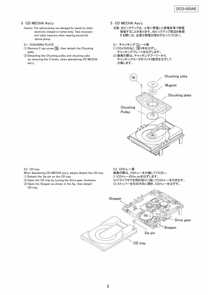
55
5
5
6
6
4
4
DCD-500AE
3. CD メカのはずしかた(1) CDメカを取り付けているねじ⑦4本をはずします。(2) コネクター (b),(c) をソケットから抜きます。※まだ FFC は抜かないこと(☆マーク)
(3) ピックアップのLD回路パターンの一部を半田付けでショートします。
(4) FFC ケーブルをソケットから抜きます。(5) FFC ケーブルをクランパーからはずします。
4. Main基板 ,Power基板のはずしかた(1) リアパネルを取り付けているねじ⑧ 3 本と端子を取り付けているねじ⑨~⑪各 1 本をはずして、リアパネルをはずします。
(2) ねじ⑫ 2本とねじ⑬ 3本をはずして、Main 基板をはずします。
(3) ねじ⑭ 1本とねじ⑮ 1本をはずして、Power 基板とパワートランスをはずします。
3. CD Mecha. Unit(1) Remove 4 screws ⑦ fixing the CD Mecha..(2) Unplug Connectors (b),(c) . ※ Do not yet exclude FFC(☆ mark).
(3) Laser short-circuit in Pick-up of CD Mecha..(4) Unplug Connector FFC from socket. (5) Release the FFC from the Clamper.
4. Main P.W.B. and Power P.W.B.(1) Remove 3 screws ⑧ ,1 screw ⑨~⑪ of the Rear
panel and detach it.(2) Remove 2 screws ⑫ ,3 screws ⑬ fixing the Main
P.W.B..(3) Remove 1 screw ⑭ ,1 screw ⑮ fixing the Power
transformer with Power P.W.B..
7
7
Clamper(b)
CD Mecha.
(c)
FFC
7
7
Main P.W.B.
Rear panel
Power transformer
with Power P.W.B.
89
1011
12
13
15
14
5
DCD-500AE
�
6
DCD-500AE
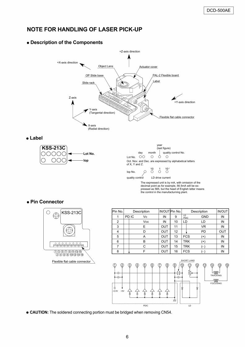
NOTE FOR HANDLING OF LASER PICK-UP
Description of the Components
Label
Pin Connector
year(last figure)
day month quality control No.
Lot No.
lop No.
Oct. Nov. and Dec. are expressed by alphabetical lettersof X, Y and Z.
10 1 10-1
LD drive currentquality control
The expressed unit is by mA, with omission of thedecimal point as for example, 56.5mA will be ex-pressed as 565, but the head of English letter meansthe control in the manufacturning plant.
Pin No. Description IN/OUT
1 PD IC Vc IN
2 Vcc IN
3 E OUT
4 D OUT
5 A OUT
6 B OUT
7 C OUT
8 F OUT
KSS-213CLot No.
lop
Slide rack
OP Slide base
Object Lens Actuator cover
PAL-2 Flexible board
Label
Flexible flat cable connector
Z-axis
Y-axis(Tangental direction)
X-axis(Radial direction)
+Z-axis direction
+X-axis direction
+Y-axis direction
1 3 5 7 9 11 13 15
2 4 6 8 10 12 14 16
KSS-213C
Flexible flat cable connector
Pin No. Description IN/OUT
9 GND IN
10 LD LD IN
11 VR IN
12 PD OUT
13 FCS (+) IN
14 TRK (+) IN
15 TRK (- ) IN
16 FCS (- ) IN
LD
PDIC
1413121110987654321 1615
TRACKING
LDPDIC
+2.5V +5V
SHORT LAND
FOCUSING
CAUTION: The soldered connecting portion must be bridged when removing CN54.
7
DCD-500AE
レーザピックアップ取扱い上の注意各部の名称
ラベル表示
コネクタ結線図
KSS-213C
1 3 5 7 9 11 13 15
2 4 6 8 10 12 14 16
KSS-213C
1413121110987654321 1615
LDPDIC
+2.5V +5V
(注意)CN54 (16P FFC ケーブル)をはずす前にハンダ接続部(ショートランド)をブリッジしてください。
ピン No. 端子名 入出力① PD IC Vc IN
② Vcc IN
③ E OUT
④ D OUT
⑤ A OUT
⑥ B OUT
⑦ C OUT
⑧ F OUT
LD
PDIC
ピン No. 端子名 入出力⑨ GND IN
⑩ LD LD IN
⑪ VR IN
⑫ PD OUT
⑬ FCS (+) IN
⑭ TRK (+) IN
⑮ TRK (-) IN
⑯ FCS (-) IN
上段 日付 月 西暦年号の末尾 品質管理No.Lot No. ○○ ○ ○ ○
但し、月表示の10、 11、 12はX、 Y、 Zで表わす。
下段 英字 10桁 1桁 小数点以下第1位○○ ○ ○ ○
IOP表示表示単位はmA、小数点は省略
頭の英字は、製造所の管理に用いる場合がある。但し、桁数は0~2桁迄とする。
8
DCD-500AE
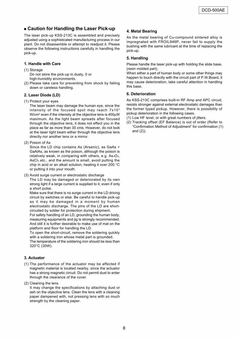
Caution for Handling the Laser Pick-up
The laser pick-up KSS-213C is assembled and precisely
adjusted using a sophisticated manufacturing process in our
plant. Do not disassemble or attempt to readjust it. Please
observe the following instructions carefully in handling the
pick-up.
1. Handle with Care
(1) Storage
Do not store the pick-up in dusty, 0 or
high-humidity environments.
(2) Please take care for preventing from shock by falling
down or careless handling.
2. Laser Diode (LD)
(1) Protect your eyes
The laser beam may damage the human eye, since the
intensity of the focused spot may reach 7x10³
W/cm2 even if the intensity at the objective lens is 400µWmaximum. As the light beam spreads after focused
through the objective lens, it does not effect you in the
place as far as more than 30 cms. However, do not look
at the laser light beam either through the objective lens
directly nor another lens or a mirror.
(2) Poison of As
Since the LD chip contains As (Arsenic), as GaAs +
GaAlAs, as known as the poison, although the poison is
relatively weak, in comparing with others, e.g. As2O3,
AsCl3 etc., and the amount is small, avoid putting the
chip in acid or an alkali solution, heating it over 200 °C
or putting it into your mouth.
(3) Avoid surge current or electrostatic discharge
The LD may be damaged or deteriorated by its own
strong light if a large current is supplied to it, even if only
a short pulse.
Make sure that there is no surge current in the LD driving
circuit by switches or else. Be careful to handle pick-up
as it may be damaged in a moment by human
electrostatic discharge. The pins of the LD are short-
circuited by solder for protection during shipment.
For safety handling of an LD, grounding the human body,
measuring equipments and jig is strongly recommended.
And still it is further desirable to make use of mat on the
platform and floor for handling the LD.
To open the short-circuit, remove the soldering quickly
with a soldering iron whose metal part is grounded.
The temperature of the soldering iron should be less than
320°C (30W).
3. Actuator
(1) The performance of the actuator may be affected if
magnetic material is located nearby, since the actuator
has a strong magnetic circuit. Do not permit dust to enter
through the clearance of the cover.
(2) Cleaning the lens
It may change the specifications by attaching dust or
ash on the objective lens. Clean the lens with a cleaning
paper dampened with, not pressing lens with so much
strength by the cleaning paper.
4. Metal Bearing
As the metal bearing of Cu-compound sintered alloy is
impregnated with FROIL946P, never fail to supply the
bushing with the same lubricant at the time of replacing the
pick-up.
5. Handling
Please handle the laser pick-up with holding the slide base.
(resin molded part).
When either a part of human body or some other things may
happen to touch directly with the circuit part of P.W.Board, it
may cause deterioration, take careful attention in handling
this base.
6. Deterioration
As KSS-213C comprises built-in RF Amp and APC circuit,
resists stronger against external electrostatic damages than
the former typed pickup. However, there is possibility of
pickup deterioration in the following cases.
(1) Low HF level, or with great numbers of jitters.
(2) Tracking offset (EF Balance) is out of order (Refer to
“Confirmation Method of Adjustment” for confirmation (1)
and (2)).
9
DCD-500AE
取扱い上の注意事項レーザーピックアップKSS-213Cは専門工場にて精密に組立調整されております。安易に分解、調整等を行わないでください。取扱いに関して次の点に注意してください。
1. 一般事項(1) 保管高温高湿下、ほこりの多い所での保存はさけてください。
(2) 精密に調整されていますので落下や不用意な取扱いによる衝撃がかからない様に注意してください。
2. 半導体レーザー(LD)(1) レーザー光に対する目の保護
LDの出力は対物レンズ出射出力で最大 400 Wですが集光された所では約7×10³W/cm 2に達します。対物レンズ集光後は光束が広がりますので30cm以上離れれば大丈夫ですが動作中のLDを直視したり、あるいは他のレンズやミラーを介して光束を観察すると危険ですから絶対に行わないでください。
(2) Asの毒性LDのチップはGaAs+GaAlAsで毒物として良く知られているAsを含んでいます。毒性は他の化合物、例えばAS2O3、ASCl3等に比較し、はるかに弱い毒性で素子1ヶ当たりは少量ですのでほとんど問題ありませんが、チップを取り出し、酸やアルカリ溶液へ入れたり、200℃以上に加熱したり、口に入れたりすることは絶対に行わないでください。
(3) サージ電流、静電気による破壊LDに大電流を流すときわめて短時間であっても自身が発する強い光によって劣化が促進され、或は破壊します。LD駆動回路にはスイッチ、その他によるサージ電流が流れない様にしてください。又、不注意に取り扱うと人体からの静電気が加わって瞬時に破壊されてしまいます。LDの端子は出荷時に輸送による静電気破壊防止の為半田でショートされています。更に、安全を期するため、取付時人体アース、計測器及び治工具のアースを必ず行ってください。又作業台、床にはアースマットを用いて接地してください。ショート部の開放はLDコネクター差し込み後、半田ゴテで行ってください。半田ゴテは金属部分が接地されたものを使用してください。半田ゴテ先温度は 320℃以下(30W)のものを使用し、すみやかに行ってください。
3. 2軸アクチュエータ(1) アクチュエータ部は強力な磁気回路を有していますので磁性体が近づくと特性が変化します。又、カバーのすきまから異物が入ることの無い様にしてください。
(2) レンズ清掃対物レンズにゴミ、ホコリ等の汚れがついたとき性能が変化します。清掃に当たってはレンズペーパーに水を少量つけ無理な力がレンズに加わらない様にして拭いてください。
4 . 軸受軸受けにはフロイル946P(関東化成工業)を塗布して有りますので、ピックアップ交換時は、必ずフロイル946Pを塗布してください。
5 . 取扱い光学ピックアップの取扱いはスライドベース(樹脂モールド部)を持って行ってください。プリント基板の回路部に人体、又は他の物体が直接触れると劣化の原因になることが有りますので、充分ご注意ください。
6 . レーザーピックアップの劣化トラッキング及びフォーカス調整が困難になったり、まったく不可能となった場合には、レーザーピックアップの劣化が考えられます。この場合はレーザーダイオードの電流値を測定して判定を行ってください。
10
DCD-500AE
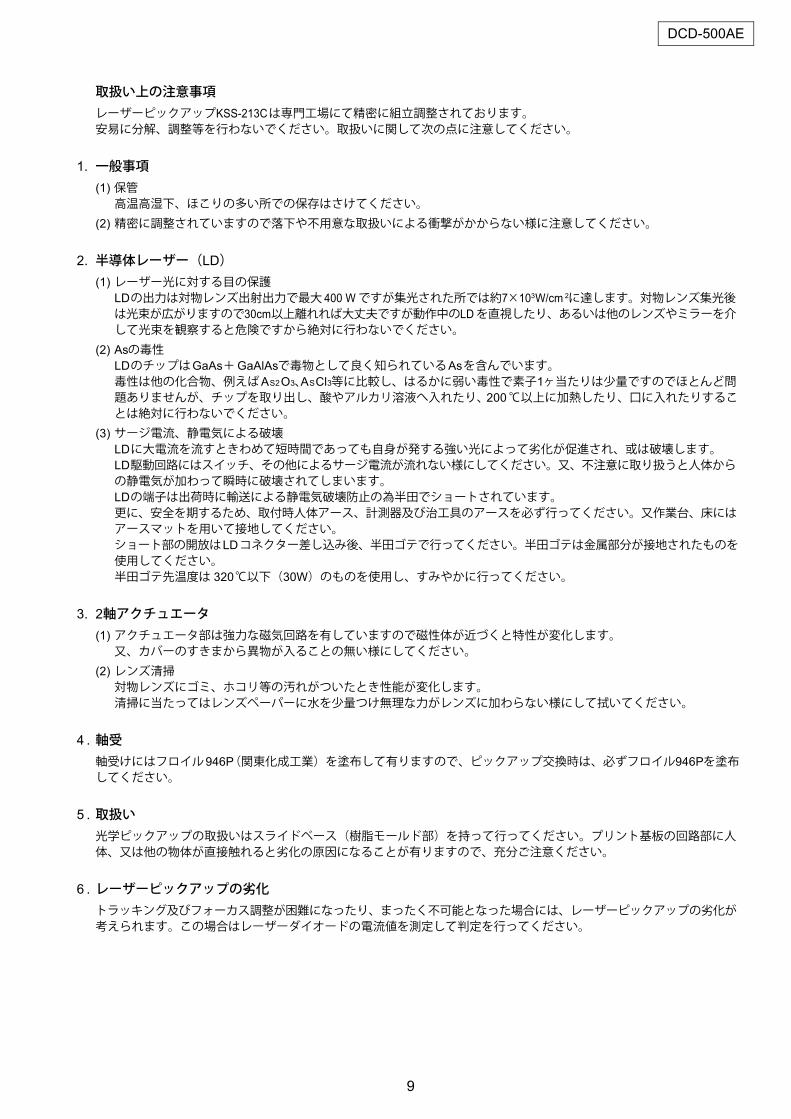
HEAT RUM MODENo Mode Operation and Function Display
1 Heat Run Mode
①When DISC is attached, POWER switch is turned to ON while pressing the Stop ( ) button on Main Unit.“DCD500DNC100” is displayed.
② Press the Skip ( ) button continuously for over 3 seconds to display the version num-ber of main micro computer.
③While the version number of main micro com-puter is displayed, press the Play/Pause ( ) button continuously for over 3 sec-onds to start heat run. is lit, is flash-ing and the other part of the FL tube is displayed in the same way as normal play mode. Count this as the 0th heat run repeti-tion.1)Play from the first to last track on disc.2)After disc playback has finished, pickup is
moved to innermost position.3)The tray is opened and the heat run repeti-
tion number is incremented (increased by 1).4)The tray is closed.5)TOC is re-read. Conduct 1) to 5) repeatedly.
・If the TIME button is pressed while operating, number of heat run is displayed for 1 second.
・While heat run, the operation of each button is not valid except the TIME button.
・ POWER switch is turned to OFF to clear heat run mode.
・If an error occurs, display the error and stop operation at that point. Number of operations held.
xx-xxxx-xx :The version number of main micro computer
xx : Number of music being playedmm:ss : Elapsed time of music being played
xxxx : Number of heat run repetition
Error Code Content E1-00 Disc cannot be detected. E2-00 Focus servo could not follow dur-
ing playback. E3-00 TOC could not be read within
specified time.
2Number of Heat Run Repetition Display Mode
Press the Skip ( ) button while the error is displayed. and are lit. And number of heat run repetition is displayed for 5 second and then the error display reappears.
xxxx : Number of heat run repetition
3
Number of Track and Elapsed Time of Track being played Display Mode
Press the Skip ( ) button while the error is displayed. and are lit. And Number of track and elapsed time of track being played in time when error occured are displayed for 5 second and then the error display reappears. xx : Number of track in time when error
occuredmm:ss : Elapsed time of track being played in
time when error occured
/
x xx - x x x x - x
D C D CN 1D 5 0 0 0 0
x x m m : s s
C D x x x x
E x - 0 0
C D x x x x
x x m m : s s
ヒートランモードNo モード 操 作 と 機 能 表 示
1 ヒートランモード
①DISC をセットした状態で 本体の Stop ( ) ボタンを押しながら、POWER スイッチをONにします。モデル名 DCD500DNC100 を表示します。
② Skip ( ) ボタンを3秒以上押し、マイコンのバージョン番号を表示させます。
③マイコンのバージョンが表示されている間にPlay/Pause ( ) ボタンを3秒以上押してヒートランを開始します。 が点灯、 が点滅します。他は通常再生モードと同じです。以下の動作を繰り返し行います。最初のヒートラン回数を0回目とします。1) ディスクの先頭曲から最終曲までを再生します。
2) ディスクの最終曲再生終了後、PUを再内周に移動させます。
3) トレイをオープンし、ヒートラン回数をカウントアップします。
4) トレイをクローズします。5) TOC リードを行い、1) の動作から再度開始します。
・ヒートラン動作中に TIME ボタンを押すと、1秒間ヒートラン回数が表示されます。
・ヒートラン時は TIME ボタン以外受け付けません。
・ヒートランモードを解除するときは、POWERスイッチをOFF にします。
・ヒートラン動作中にエラーが発生すると、エラーを表示し、その時の状態で停止します。動作回数は保持されます。
xx-xxxx-xx :メインマイコンのバージョン番号
xx :再生中トラック番号mm:ss :再生時間
xxxx :ヒートラン回数
xxxx :ヒートラン回数
エラーコード 内 容 E1-00 ディスクの検出ができない。 E2-00 再生中にフォーカスが追従できな
かった時があった。 E3-00 TOC が規定時間内に読めない。
2エラー時のヒートラン回数表示モード
エラー表示中に Skip ( ) ボタンを押すと、 と が点灯し、ヒートラン回数を 5秒間
表示して、エラー表示に戻ります。
xxxx :ヒートラン回数
3エラー時の曲番と時間表示モード
エラー表示中に Skip ( ) ボタンを押すと、と が点灯し、エラー発生時の曲番と再
生時間を 5秒間表示して、エラー表示に戻ります。
xx :エラー発生時のトラック番号mm:ss :エラー発生時の再生時間
/
x xx - x x x x - x
D C D CN 1D 5 0 0 0 0
x x m m : s s
C D x x x x
C D x x x x
E x - 0 0
C D x x x x
x x m m : s s
11
DCD-500AE
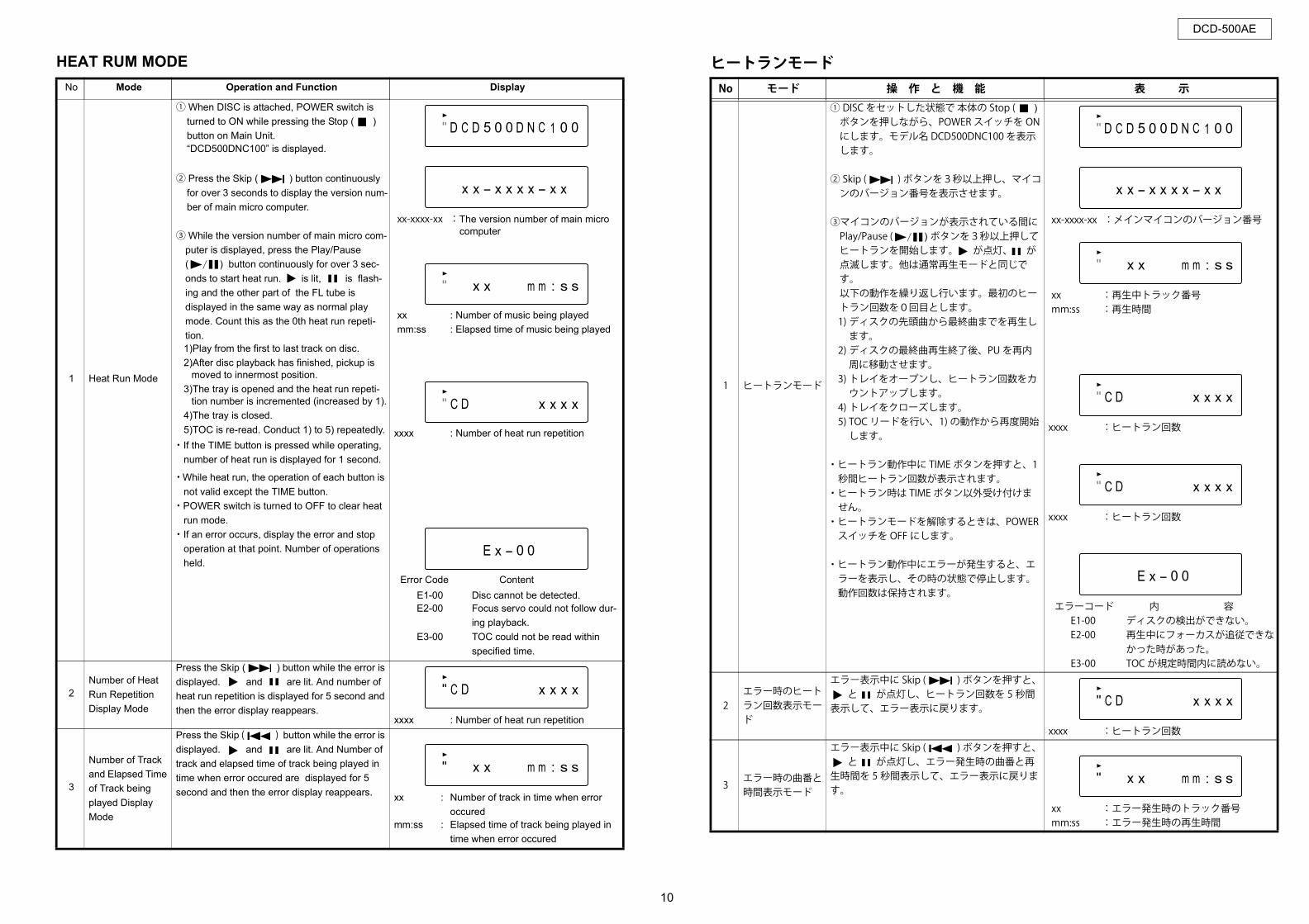
SERVICE MODENo Mode Operation and Function Display
1
Version Number of Micro Com-puter Display Mode
① POWER switch is turned to ON while press-ing the Stop ( ) button on Main Unit.
② Press the Skip ( ) button continuously for over 3 seconds to display the version num-ber of main micro computer.
xx-xxxx-xx : The version number of main micro computer
2Number of Laser ON Time Count Display Mode
① POWER switch is turned to ON while press-ing the Stop ( ) button on Main Unit.
② Press the Skip ( ) button continuously for over 3 seconds to display number of Laser ON time count.
・The number of time when the normal playback time the Laser is turned to ON is incremented (increased by 1) in every 15 minutes. The accumulation number of times is recorded to memory whenever count it.
xxxx : Number of Laser ON time count
3 Initialize Mode
POWER switch is turned to ON while pressing the TIME button on Main Unit.・Brightness setting of display becomes 100%
(default).・The accumulation number of laser on time is
cleared, and a count becomes 0000.
Not special display
x xx - x x x x - x
L D - x x x x
サービスモードNo モード 操 作 と 機 能 表 示
1マイコンのバージョン番号表示モード
①本体の Stop ( ) ボタンを押しながら、POWER スイッチをONにします。② Skip ( ) ボタンを3秒以上押し、マイコンのバージョン番号を表示させます。
xx-xxxx-xx :メインマイコンのバージョン番号
2レーザーON時間カウント回数表示モード
①本体の Stop ( ) ボタンを押しながら、POWER スイッチをONにします。② Skip ( ) ボタンを3秒以上押し、レーザー ON時間カウント回数を表示させます。
・通常再生時にレーザーをONにしている時間を15分毎にカウントアップします。カウント時に累積回数を記憶します。
xxxx :レーザーON時間カウント回数
3 初期化モード
本体 TIME ボタンを押しながら、POWER スイッチをONにします。・FL 管の輝度設定を 100%( デフォルト ) にします。・レーザー ON時間カウントの累積回数をクリアします。
なし
x xx - x x x x - x
L D - x x x x
12
DCD-500AE
CD TEST MODE & SERVICE MODE
13
DCD-500AE
TROUBLE SHOOTING
14
DCD-500AE
15
DCD-500AE
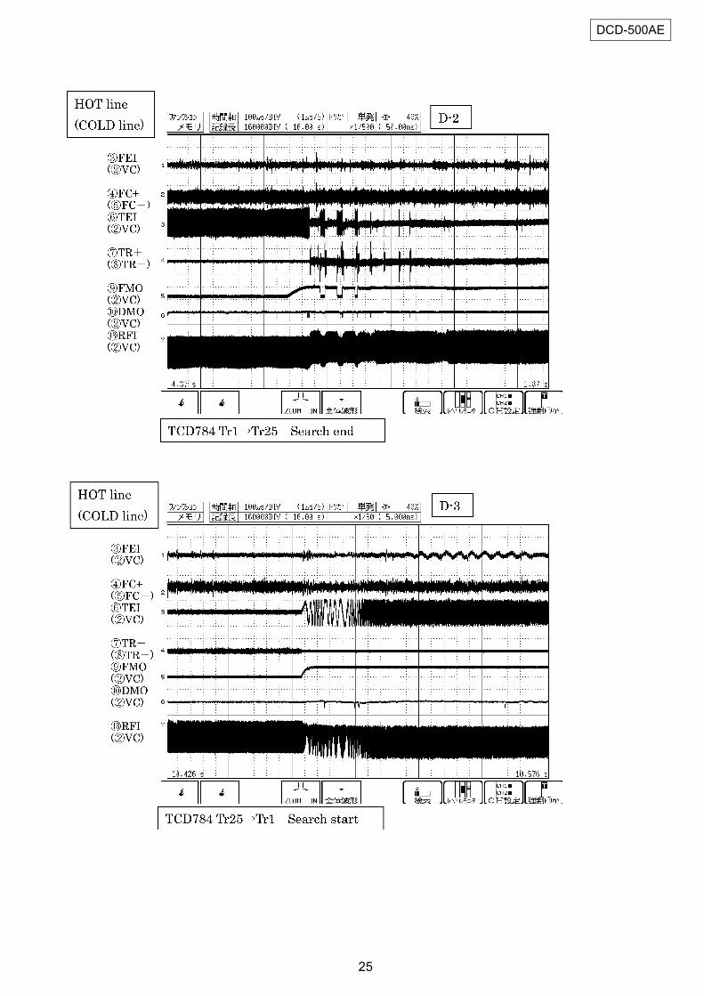
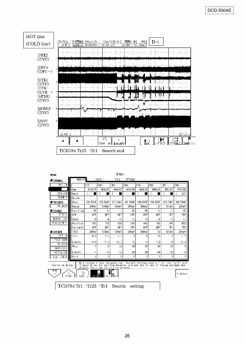
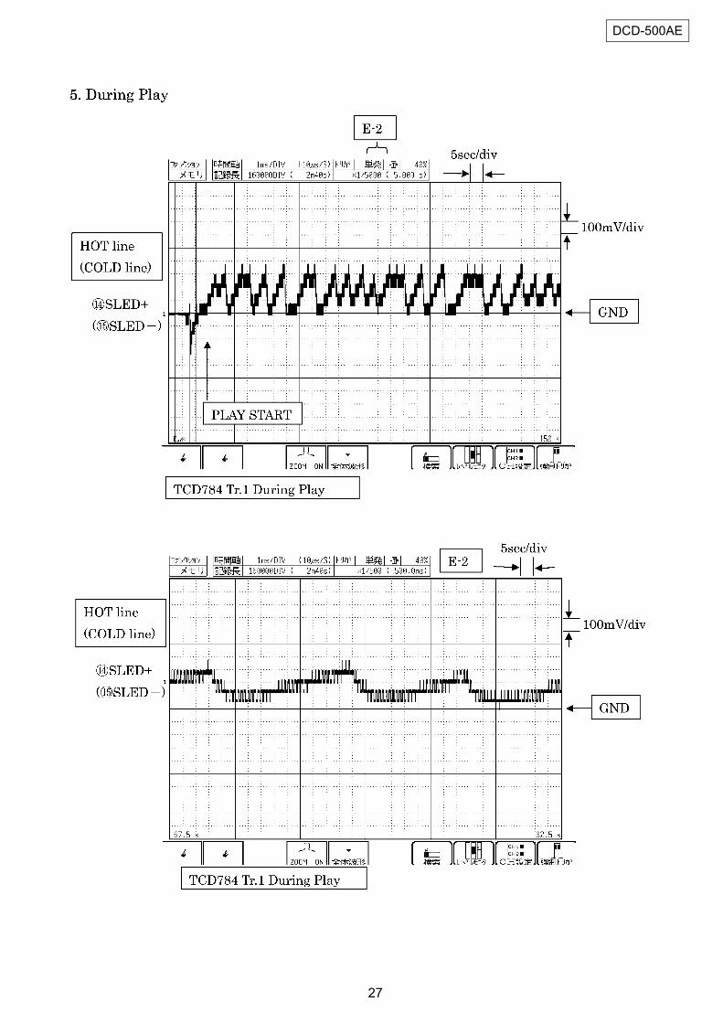
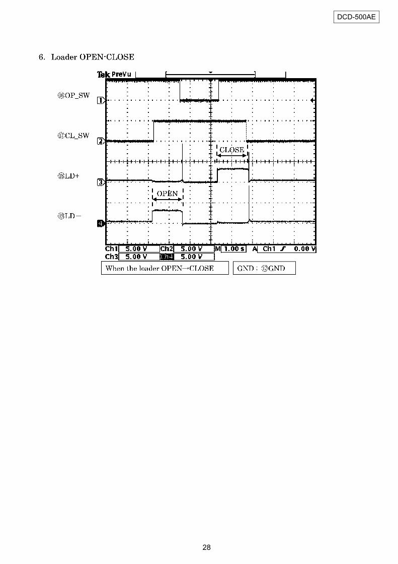
WAVEFORMS
MAIN P.W.B. UNIT
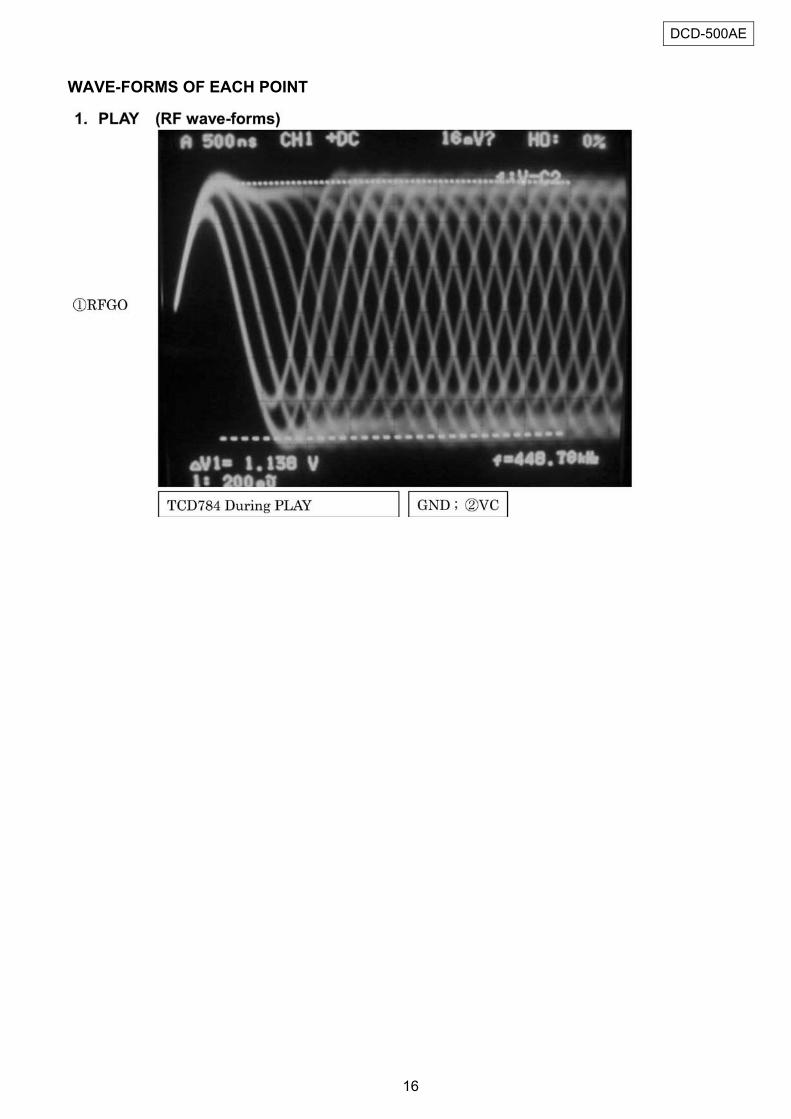
16
DCD-500AE
WAVE-FORMS OF EACH POINT
17
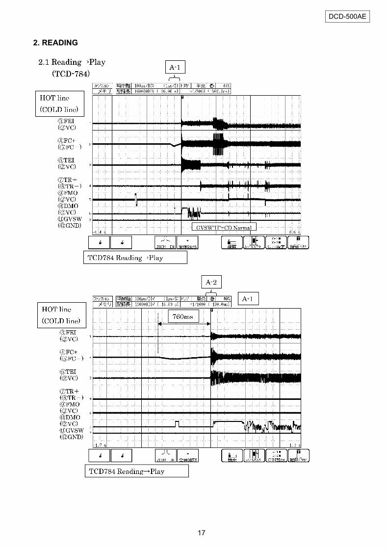
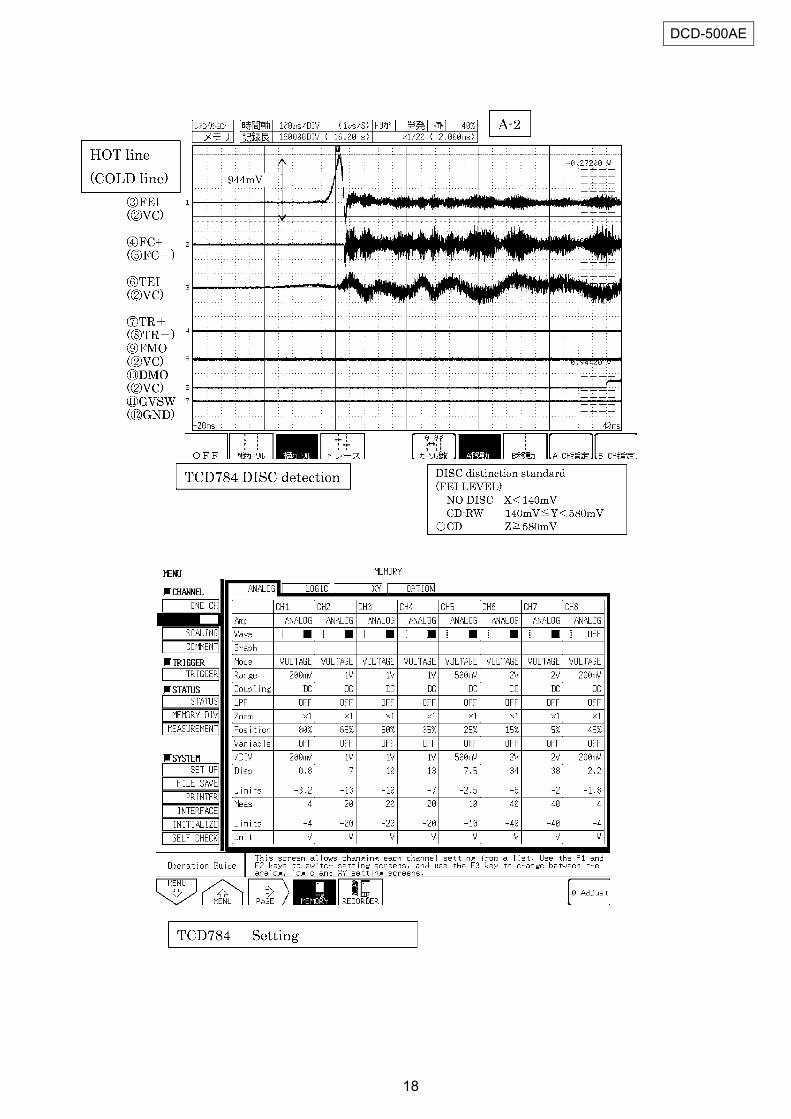
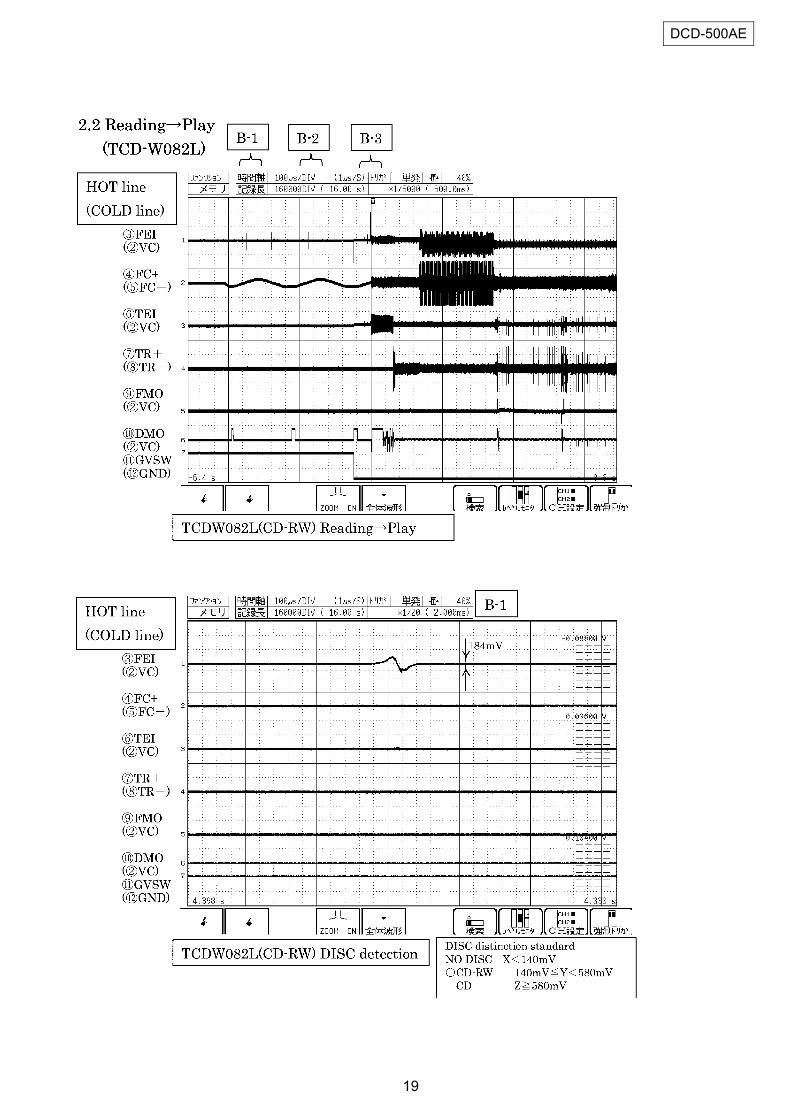
DCD-500AE
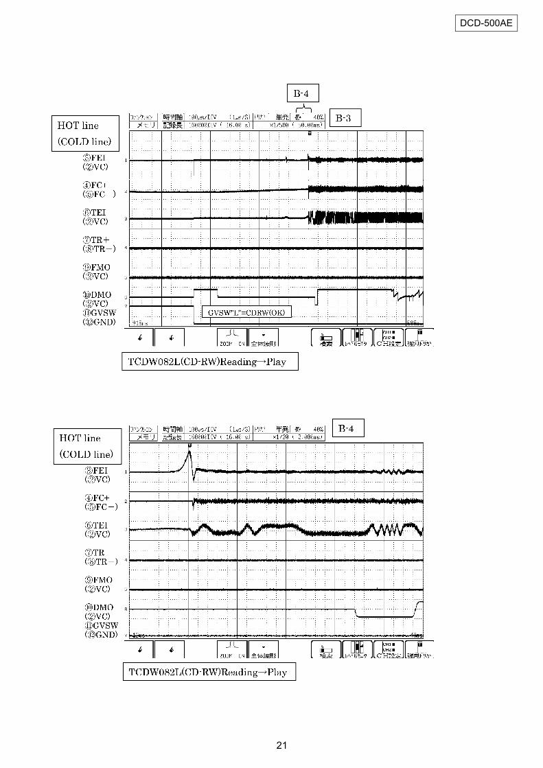
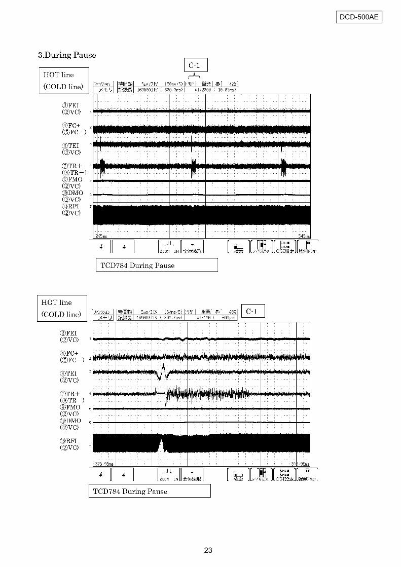
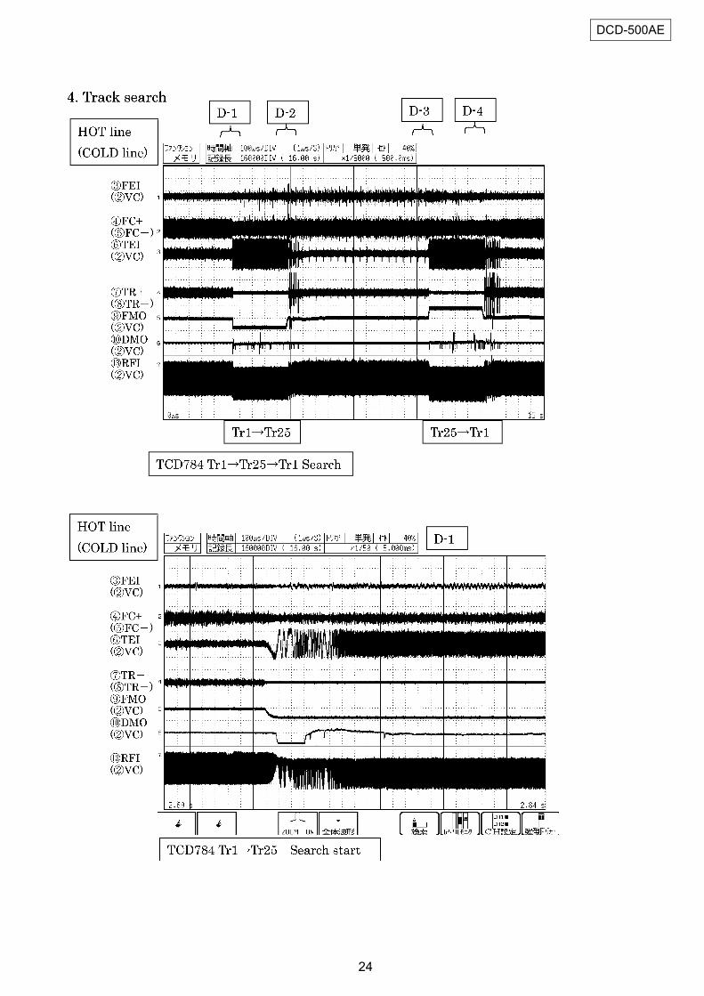
2. READING
18
DCD-500AE
19
DCD-500AE
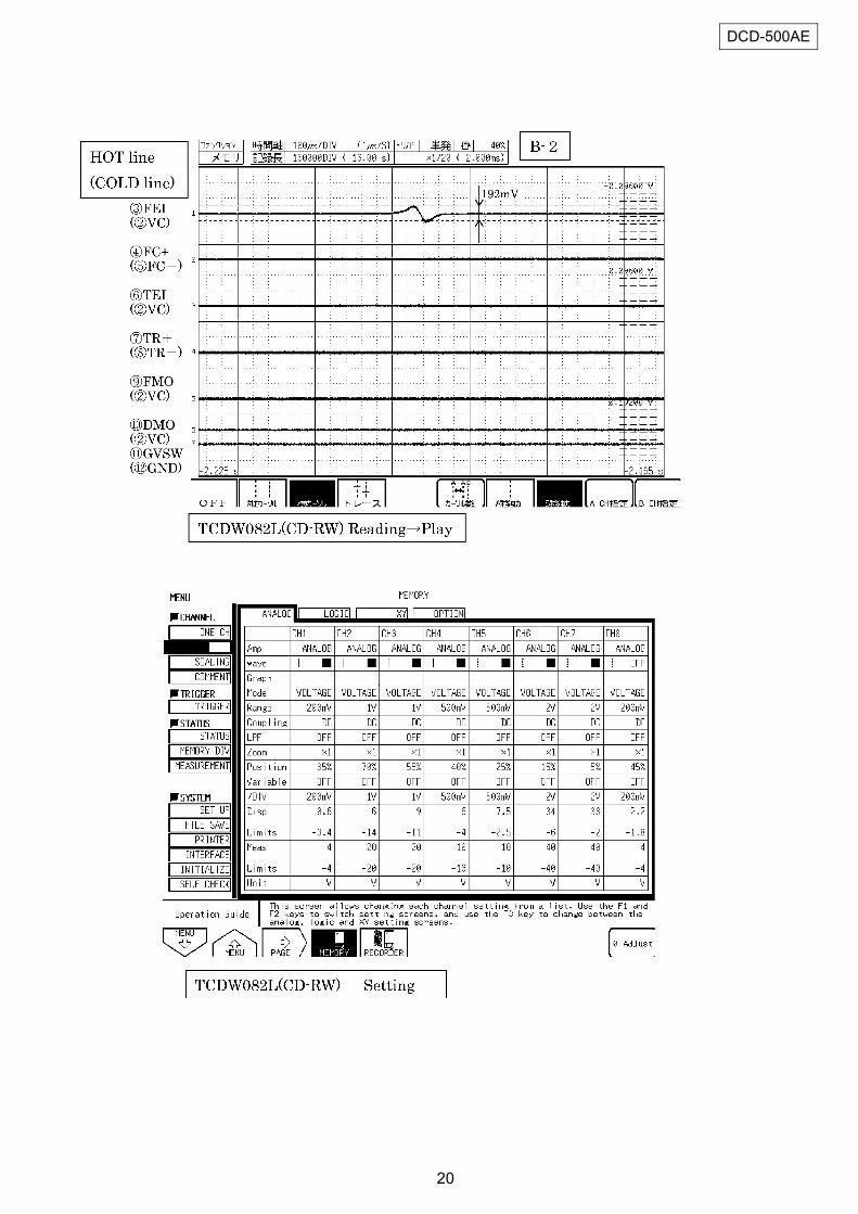
20
DCD-500AE
21
DCD-500AE

22
DCD-500AE
23
DCD-500AE
24
DCD-500AE
25
DCD-500AE
26
DCD-500AE
27
DCD-500AE
28
DCD-500AE
29
DCD-500AE
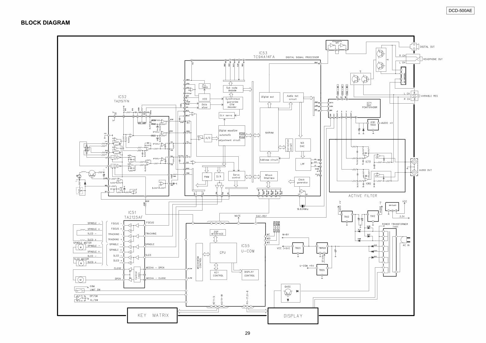
BLOCK DIAGRAM
30
DCD-500AE
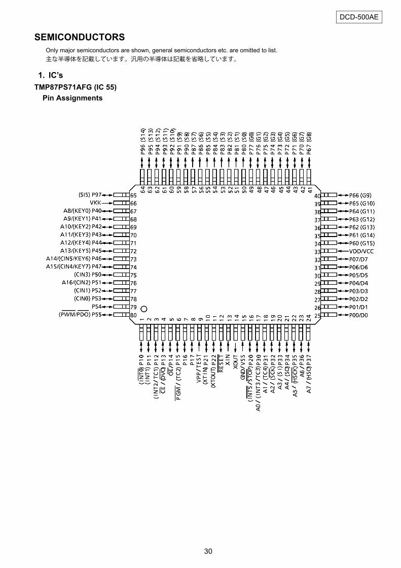
SEMICONDUCTORSOnly major semiconductors are shown, general semiconductors etc. are omitted to list.主な半導体を記載しています。汎用の半導体は記載を省略しています。
1. IC’sTMP87PS71AFG (IC 55) Pin Assignments
31
DCD-500AE
32
DCD-500AE
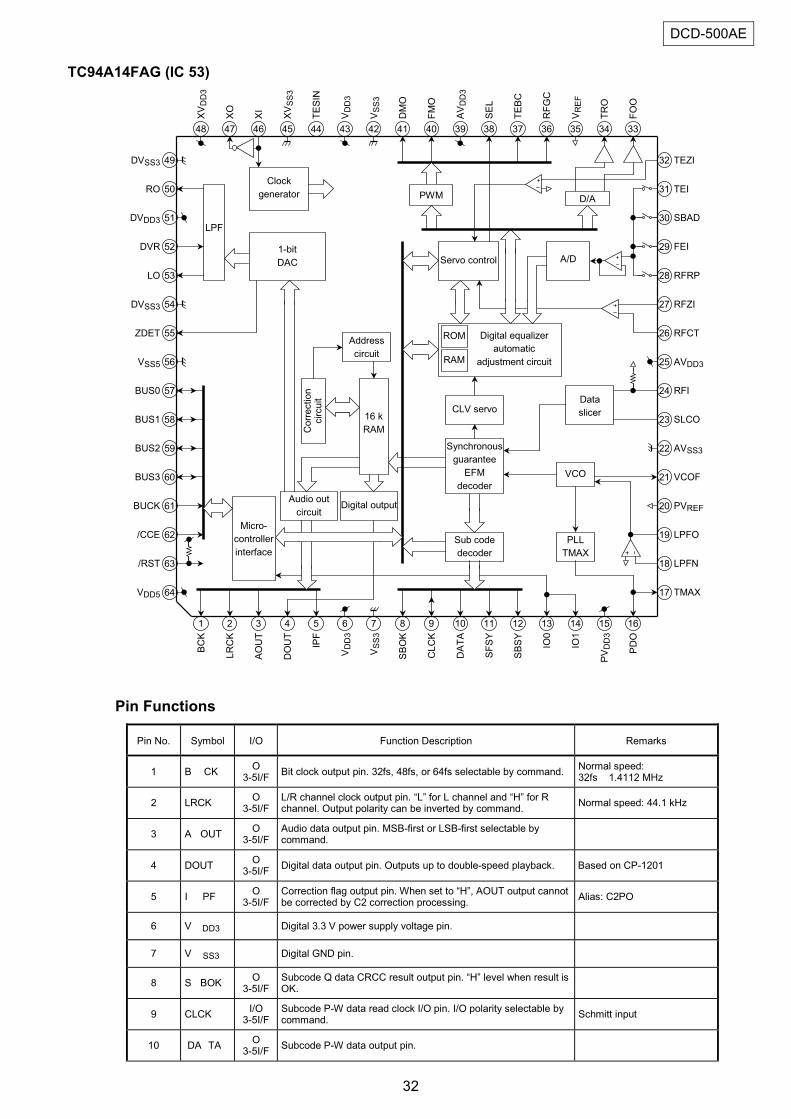
TC94A14FAG (IC 53)
Pin Functions
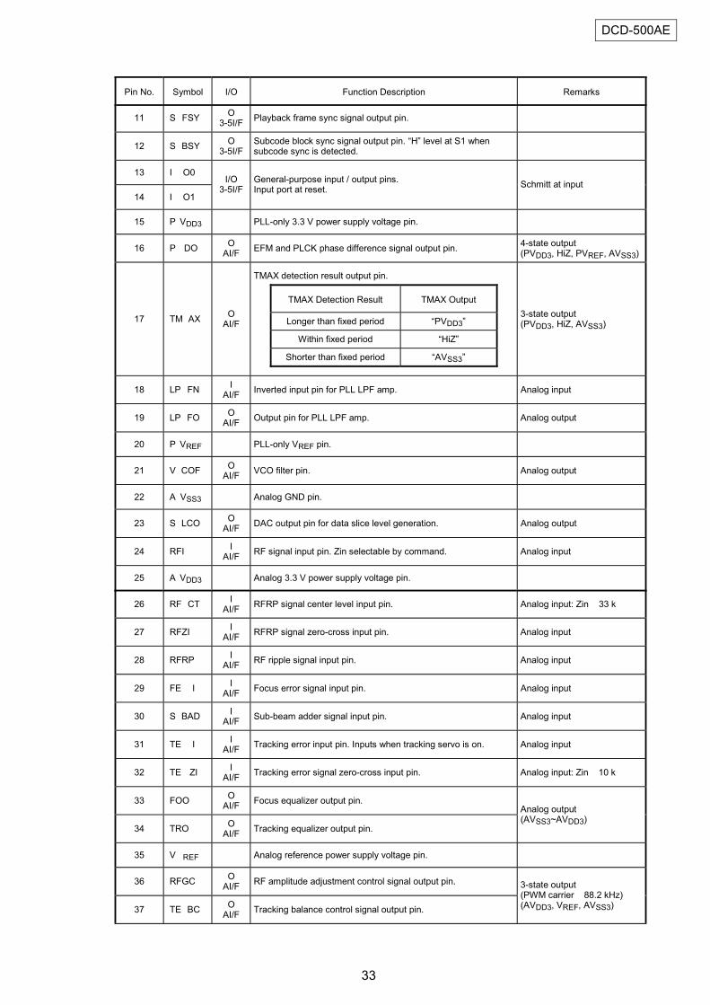
Pin No. Symbol I/O Function Description Remarks
1 B CKO
3-5I/FBit clock output pin. 32fs, 48fs, or 64fs selectable by command.
Normal speed:32fs 1.4112 MHz
2 LRCKO
3-5I/FL/R channel clock output pin. “L” for L channel and “H” for Rchannel. Output polarity can be inverted by command.
Normal speed: 44.1 kHz
3 A OUTO
3-5I/FAudio data output pin. MSB-first or LSB-first selectable bycommand.
4 DOUTO
3-5I/FDigital data output pin. Outputs up to double-speed playback. Based on CP-1201
5 I PFO
3-5I/FCorrection flag output pin. When set to “H”, AOUT output cannotbe corrected by C2 correction processing.
Alias: C2PO
6 V DD3 Digital 3.3 V power supply voltage pin.
7 V SS3 Digital GND pin.
8 S BOKO
3-5I/FSubcode Q data CRCC result output pin. “H” level when result isOK.
9 CLCKI/O3-5I/F
Subcode P-W data read clock I/O pin. I/O polarity selectable bycommand.
Schmitt input
10 DA TAO
3-5I/FSubcode P-W data output pin.
DVSS3
RO
DVDD3
DVR
LO
DVSS3
ZDET
VSS5
BUS0
BUS1
BUS2
BUS3
BUCK
/CCE
/RST
VDD5
TEZI
TEI
SBAD
FEI
RFRP
RFZI
RFCT
AVDD3
RFI
SLCO
AVSS3
VCOF
PVREF
LPFO
LPFN
TMAX
49
50
51
52
53
54
55
56
57
58
59
60
61
62
63
64
XVDD3
XO
XI
XVSS3
TESIN
VDD3
VSS3
DMO
FMO
AVDD3
SEL
TEBC
RFGC
VREF
TRO
FOO
48
32
3347 46 45 44 43 42 41 40 39 38 37 36 35 34
BCK
LRCK
AOUT
DOUT
IPF
VDD3
VSS3
SBOK
CLCK
DATA
SFSY
SBSY
IO0
IO1
PVDD3
PDO
1 162 3 4 5 6 7 8 9 10 11 12 13 14 15
31
30
29
28
27
26
25
24
23
22
21
20
19
18
17
Micro-
controller
interface
Audio out
circuitDigital output
Correction
circuit
16 k
RAM
Address
circuit
LPF
Sub code
decoder
CLV servo
ROM
RAM
Digital equalizer
automatic
adjustment circuit
Servo control
PWM
A/D
D/A
Data
slicer
VCO
PLL
TMAX
Clock
generator
1-bit
DAC
Synchronous
guarantee
EFM
decoder
33
DCD-500AE
Pin No. Symbol I/O Function Description Remarks
26 RF CTI
AI/FRFRP signal center level input pin. Analog input: Zin 33 k
27 RFZII
AI/FRFRP signal zero-cross input pin. Analog input
28 RFRPI
AI/FRF ripple signal input pin. Analog input
29 FE II
AI/FFocus error signal input pin. Analog input
30 S BADI
AI/FSub-beam adder signal input pin. Analog input
31 TE II
AI/FTracking error input pin. Inputs when tracking servo is on. Analog input
32 TE ZII
AI/FTracking error signal zero-cross input pin. Analog input: Zin 10 k
33 FOOOAI/F
Focus equalizer output pin.
34 TROOAI/F
Tracking equalizer output pin.
Analog output(AVSS3~AVDD3)
35 V REF Analog reference power supply voltage pin.
36 RFGCOAI/F
RF amplitude adjustment control signal output pin.
37 TE BCOAI/F
Tracking balance control signal output pin.
3-state output(PWM carrier 88.2 kHz)(AVDD3, VREF, AVSS3)
11 S FSYO
3-5I/FPlayback frame sync signal output pin.
12 S BSYO
3-5I/FSubcode block sync signal output pin. “H” level at S1 whensubcode sync is detected.
13 I O0
14 I O1
I/O3-5I/F
General-purpose input / output pins.Input port at reset.
Schmitt at input
15 P VDD3 PLL-only 3.3 V power supply voltage pin.
16 P DOOAI/F
EFM and PLCK phase difference signal output pin.4-state output(PVDD3, HiZ, PVREF, AVSS3)
17 TM AXOAI/F
TMAX detection result output pin.
TMAX Detection Result TMAX Output
Longer than fixed period “PVDD3”
Within fixed period “HiZ”
Shorter than fixed period “AVSS3”
3-state output(PVDD3, HiZ, AVSS3)
18 LP FNI
AI/FInverted input pin for PLL LPF amp. Analog input
19 LP FOOAI/F
Output pin for PLL LPF amp. Analog output
20 P VREF PLL-only VREF pin.
21 V COFOAI/F
VCO filter pin. Analog output
22 A VSS3 Analog GND pin.
23 S LCOOAI/F
DAC output pin for data slice level generation. Analog output
24 RFII
AI/FRF signal input pin. Zin selectable by command. Analog input
25 A VDD3 Analog 3.3 V power supply voltage pin.
34
DCD-500AE
Pin No. Symbol I/O Function Description Remarks
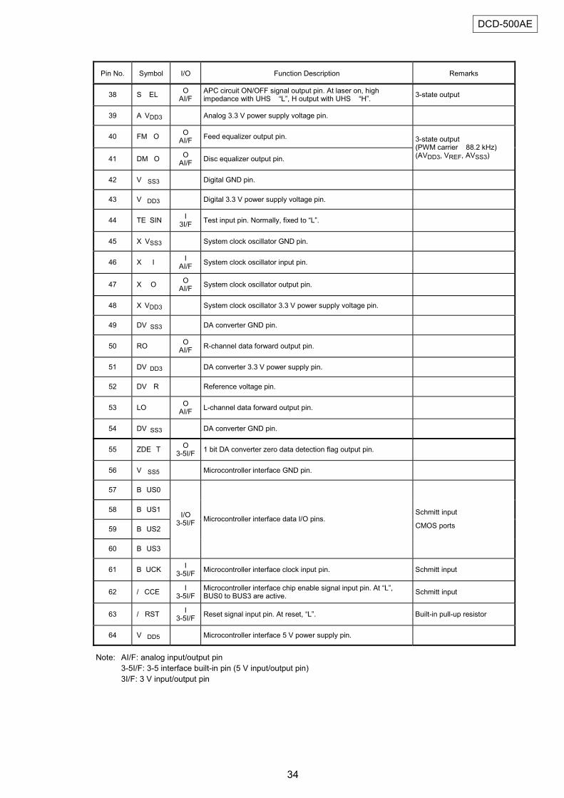
55 ZDE TO
3-5I/F1 bit DA converter zero data detection flag output pin.
56 V SS5 Microcontroller interface GND pin.
57 B US0
58 B US1
59 B US2
60 B US3
I/O3-5I/F
Microcontroller interface data I/O pins.Schmitt input
CMOS ports
61 B UCKI
3-5I/FMicrocontroller interface clock input pin. Schmitt input
62 / CCEI
3-5I/FMicrocontroller interface chip enable signal input pin. At “L”,BUS0 to BUS3 are active.
Schmitt input
63 / RSTI
3-5I/FReset signal input pin. At reset, “L”. Built-in pull-up resistor
64 V DD5 Microcontroller interface 5 V power supply pin.
Note: AI/F: analog input/output pin
3-5I/F: 3-5 interface built-in pin (5 V input/output pin)
3I/F: 3 V input/output pin
38 S ELOAI/F
APC circuit ON/OFF signal output pin. At laser on, highimpedance with UHS “L”, H output with UHS “H”.
3-state output
39 A VDD3 Analog 3.3 V power supply voltage pin.
40 FM OOAI/F
Feed equalizer output pin.
41 DM OOAI/F
Disc equalizer output pin.
3-state output(PWM carrier 88.2 kHz)(AVDD3, VREF, AVSS3)
42 V SS3 Digital GND pin.
43 V DD3 Digital 3.3 V power supply voltage pin.
44 TE SINI3I/F
Test input pin. Normally, fixed to “L”.
45 X VSS3 System clock oscillator GND pin.
46 X II
AI/FSystem clock oscillator input pin.
47 X OOAI/F
System clock oscillator output pin.
48 X VDD3 System clock oscillator 3.3 V power supply voltage pin.
49 DV SS3 DA converter GND pin.
50 ROOAI/F
R-channel data forward output pin.
51 DV DD3 DA converter 3.3 V power supply pin.
52 DV R Reference voltage pin.
53 LOOAI/F
L-channel data forward output pin.
54 DV SS3 DA converter GND pin.
35
DCD-500AE
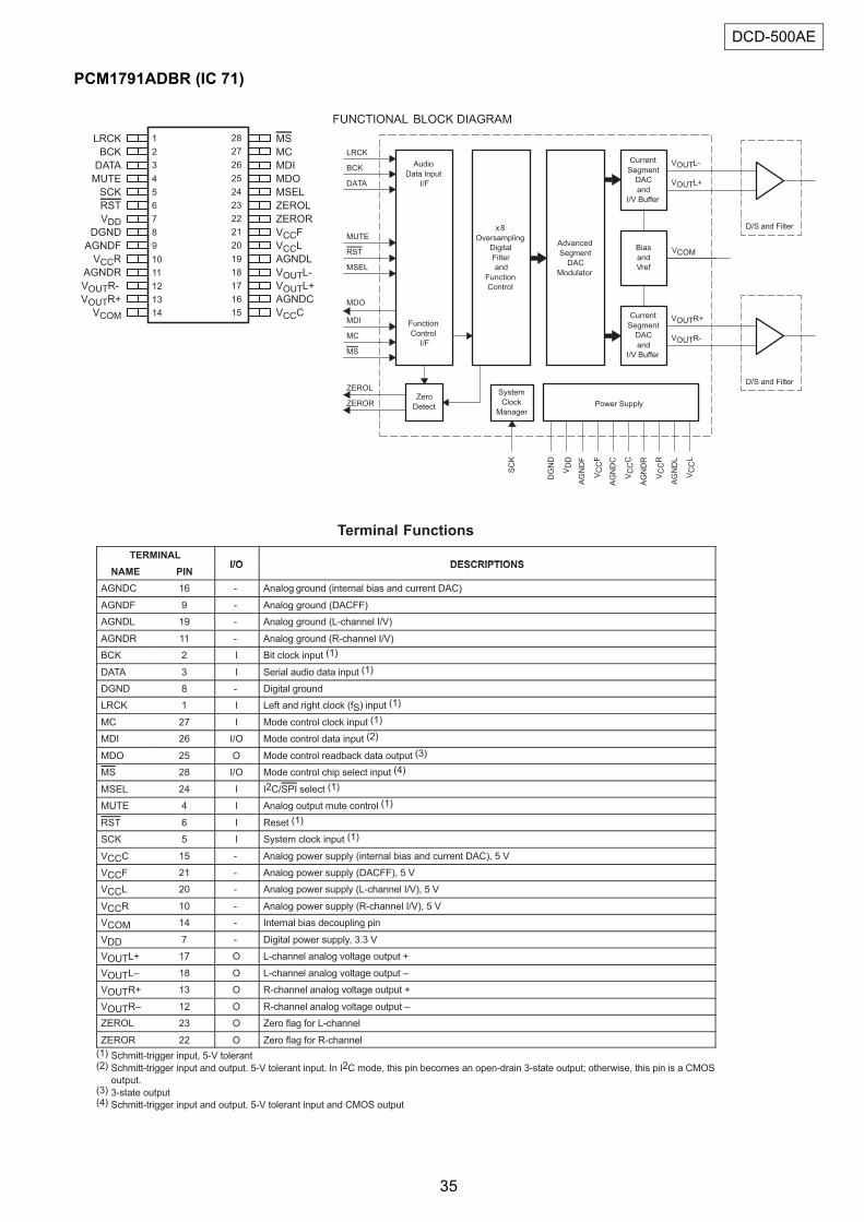
PCM1791ADBR (IC 71)
1
2
3
4
5
6
7
8
9
10
11
12
13
14
28
27
26
25
24
23
22
21
20
19
18
17
16
15
LRCK
BCK
DATA
MUTE
SCK
RST
VDDDGND
AGNDF
VCCR
AGNDR
VOUTR-
VOUTR+
VCOM
MS
MC
MDI
MDO
MSEL
ZEROL
ZEROR
VCCF
VCCL
AGNDL
VOUTL-
VOUTL+
AGNDC
VCCC
FUNCTIONAL BLOCK DIAGRAM
Power Supply
RST
SCK
Advanced
Segment
DAC
Modulator
VOUTL+
VOUTL-
Bias
and
Vref
VCCF
VDD
AGNDR
VCCR
AGNDL
AGNDF
D/S and Filterx8
Oversampling
Digital
Filter
and
Function
Control
Audio
Data Input
I/F
LRCK
BCK
DATA
MDO
MDI
MC
MS
AGNDC
VCCC
DGND
Current
Segment
DAC
and
I/V Buffer
VCOM
Function
Control
I/F
Zero
Detect
ZEROL
ZEROR
System
Clock
Manager
MSEL
MUTE
VCCL
VOUTR-
VOUTR+
D/S and Filter
Current
Segment
DAC
and
I/V Buffer
Terminal Functions
TERMINALI/O DESCRIPTIONS
NAME PINI/O DESCRIPTIONS
AGNDC 16 - Analog ground (internal bias and current DAC)
AGNDF 9 - Analog ground (DACFF)
AGNDL 19 - Analog ground (L-channel I/V)
AGNDR 11 - Analog ground (R-channel I/V)
BCK 2 I Bit clock input (1)
DATA 3 I Serial audio data input (1)
DGND 8 - Digital ground
LRCK 1 I Left and right clock (fS) input(1)
MC 27 I Mode control clock input (1)
MDI 26 I/O Mode control data input (2)
MDO 25 O Mode control readback data output (3)
MS 28 I/O Mode control chip select input (4)
MSEL 24 I I2C/SPI select (1)
MUTE 4 I Analog output mute control (1)
RST 6 I Reset (1)
SCK 5 I System clock input (1)
VCCC 15 - Analog power supply (internal bias and current DAC), 5 V
VCCF 21 - Analog power supply (DACFF), 5 V
VCCL 20 - Analog power supply (L-channel I/V), 5 V
VCCR 10 - Analog power supply (R-channel I/V), 5 V
VCOM 14 - Internal bias decoupling pin
VDD 7 - Digital power supply, 3.3 V
VOUTL+ 17 O L-channel analog voltage output +
VOUTL– 18 O L-channel analog voltage output –
VOUTR+ 13 O R-channel analog voltage output +
VOUTR– 12 O R-channel analog voltage output –
ZEROL 23 O Zero flag for L-channel
ZEROR 22 O Zero flag for R-channel
(1) Schmitt-trigger input, 5-V tolerant(2) Schmitt-trigger input and output. 5-V tolerant input. In I2C mode, this pin becomes an open-drain 3-state output; otherwise, this pin is a CMOS
output.(3) 3-state output(4) Schmitt-trigger input and output. 5-V tolerant input and CMOS output
36
DCD-500AE
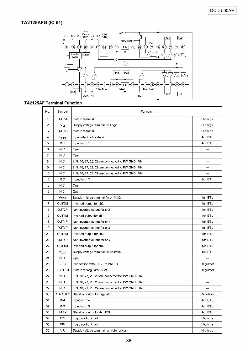
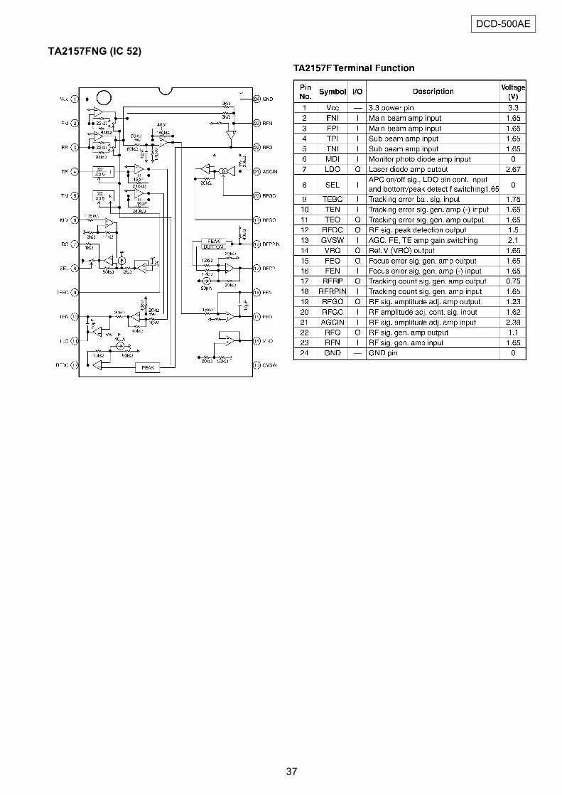
TA2125AFG (IC 51)
TA2125AF Terminal Function
37
DCD-500AE
TA2157FNG (IC 52)
38
DCD-500AE
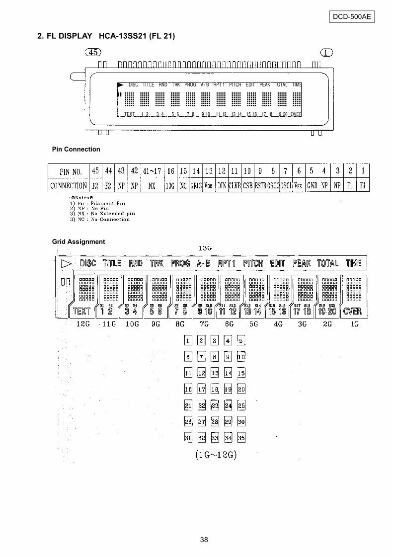
2. FL DISPLAY HCA-13SS21 (FL 21)
Pin Connection
Grid Assignment
39
DCD-500AE
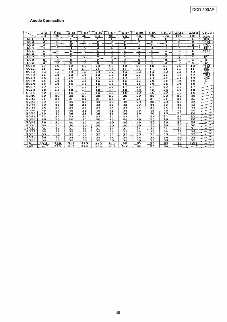
Anode Connection
40
DCD-500AE
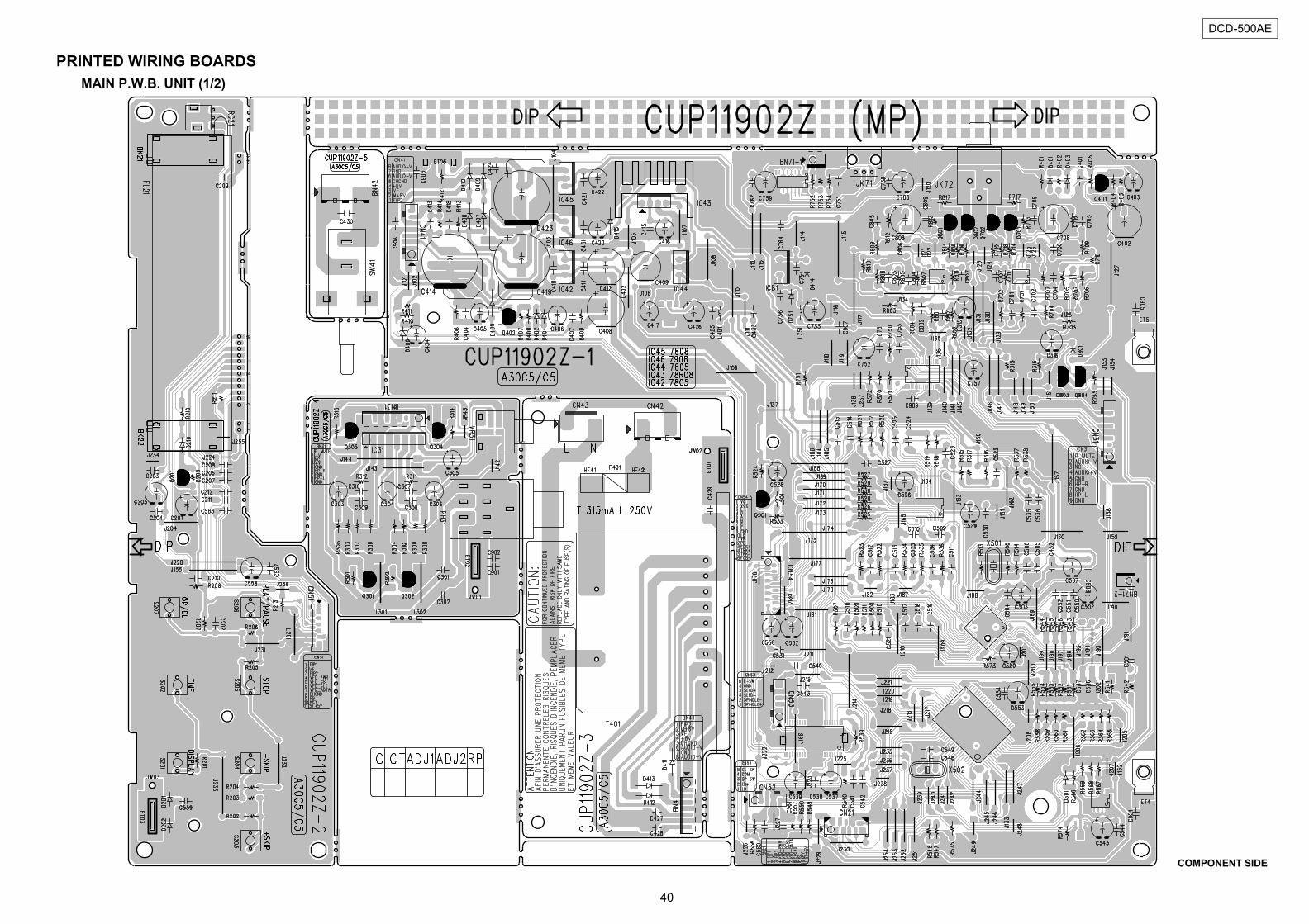
PRINTED WIRING BOARDSMAIN P.W.B. UNIT (1/2)
COMPONENT SIDE
41
DCD-500AE
MAIN P.W.B. UNIT (2/2)
FOIL SIDE
42
DCD-500AE
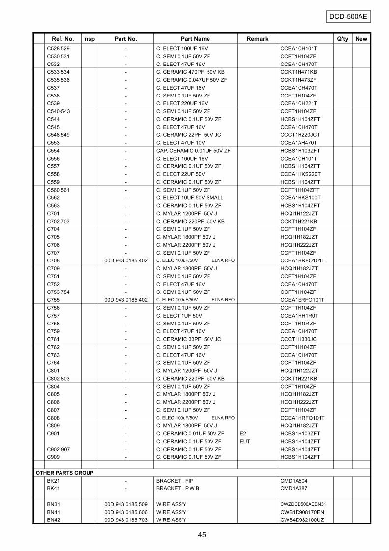
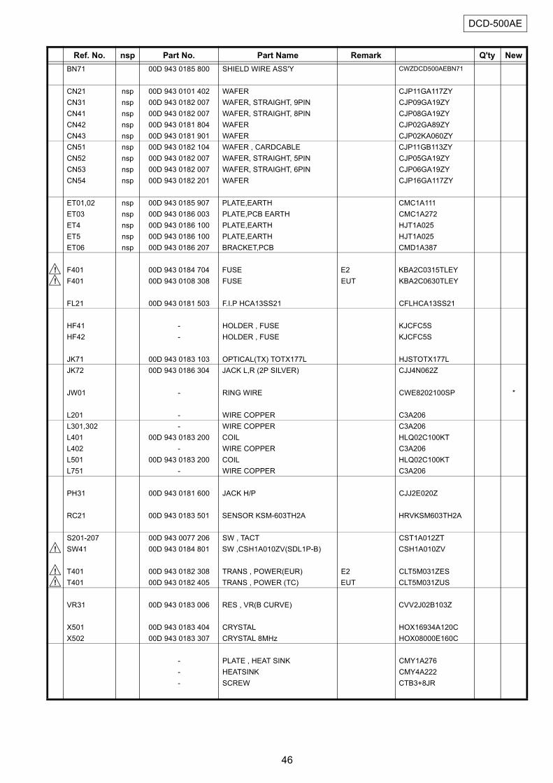
NOTE FOR PARTS LIST • Part indicated with the mark "nsp" are not always in stock and possibly to
take a long period of time for supplying, or in some case supplying of part may be refused.
• When ordering of part, clearly indicate "1" and "I" (i) to avoid mis-supplying.
• Ordering part without stating its part number can not be supplied. • Part indicated with the mark "★ " is not illustrated in the exploded view. • Not including General-purpose Carbon Film Resistor in the P.W.Board
parts list. (Refer to the Schematic Diagram for those parts.) • Not including General-purpose Carbon Chip Resistor in the P.W.Board
parts list. (Refer to the Schematic Diagram for those parts.) WARNING: Parts marked with this symbol ! have critical characteristics. Use ONLY replacement parts recommended by the manufacturer.
ss
ss
s s
s s
ss
ss
RD : 2B : 1/8 W F : ±1% P :RC : 2E : 1/4 W G : ±2% NL :RS : 2H : 1/2 W J : ±5% NB :RW : 3A : 1 W K : ±10% FR :RN : 3D : 2 W M : ±20% F :RK : 3F : 3 W
3H : 5 W
RN 14K 2E 182 G FR
∗ 18 2 1800 =1.8k
0
2
1R 2 1.2
1
2 R
CE 04W 1H 2R2 M BP
CE : 0J : 6.3 V F : ±1% HS :
CA : 1A : 10 V G : ±2% BP :CS : 1C : 16 V J : ±5% HR :CQ : 1E : 25 V K : ±10% DL :CK : 1V : 35 V M : ±20% HF :CC : 1H : 50 V Z : +80% U : ULCP : 2A : 100 V −20% C : CSACM : 2B : 125 V P : +100% W : UL-CSACF : 2C : 160 V − 0% F :CH : 2D : 200 V C : ±0.25pF
2E : 250 V D : ±0.5pF2H : 500 V = :
2J : 630 V
∗
22 2 2200µF
02
µF
22 2 2200pF=0.0022µF
0
2
pF pF
22 1 220pF
2
(0 2 )0
(0 0 1 )
2R 2 2.2µF
12 R
µF
AC
RD : Carbon 2B : 1/8W F : ±1% P : Pulse-resistant typeRC : Composition 2E : 1/4W G : ±2% NL : Low noise typeRS : Metal oxide film 2H : 1/2W J : ±5% NB : Non-burning typeRW : Winding 3A : 1W K : ±10% FR : Fuse-resistorRN : Metal film 3D : 2W M : ±20% F : Lead wire formingRK : Metal mixture 3F : 3W
3H : 5W
CE : Aluminum foil 0J : 6.3V F : ±1% HS : High stability typeelectrolytic
CA : Aluminum solid 1A : 10V G : ±2% BP : Non-polar typeelectrolytic
CS : Tantalum electrolytic 1C : 16V J : ±5% HR : Ripple-resistant typeCQ : Film 1E : 25V K : ±10% DL : For change and dischargeCK : Ceramic 1V : 35V M : ±20% HF : For assuring high
requencyCC : Ceramic 1H : 50V Z : +80% U : UL partCP : Oil 2A : 100V –20% C : CSA partCM : Mica 2B : 125V P : +100% W : UL-CSA typeCF : Metallized 2C : 160V –0% F : Lead wire formingCH : Metallized 2D : 200V C : ±0.25pF
2E : 250V D : ±0.5pF2H : 500V = : Others2J : 630V
lllll Resistors
Ex.: RN 14K 2E 182 G FRType Shape Power Resist- Allowable Others
and per- ance errorformance
] Resistance
1 8 2 ⇒ 1800 ohm = 1.8 kohmIndicates number of zeros after effective number.2-digit effective number.
• Units: ohm
1 R 2 ⇒ 1.2 ohm1-digit effective number.2-digit effective number, decimal point indicated by R.
• Units: ohm
lllll Capacitors
Ex.: CE 04W 1H 2R2 M BPType Shape Dielectric Capacity Allowable Others
and per- strength errorformance
] Capacity (electrolyte only)
2 2 2 ⇒ 2200µFIndicates number of zeros after effective number.2-digit effective number.
• Units: µF.
2 R 2 ⇒ 2.2µF1-digit effective number.2-digit effective number, decimal point indicated by R.
• Units: µF.
] Capacity (except electrolyte)
2 2 2 ⇒ 2200pF=0.0022µF(More than 2) Indicates number of zeros after effective number.
2-digit effective number.• Units: pF.
2 2 1 ⇒ 220pF(0 or 1) Indicates number of zeros after effective number.
2-digit effective number.• Units: pF.
• When the dielectric strength is indicated in AC, "AC" is included after the dieelectricstrength value.
部品表について1.nsp 印の部品は常時在庫していませんので供給に長時間を要すること
があります。場合によっては、供給をお断りすることがあります。
2.部品を発注する際は特に数字の " 1 " と英字の "I" との区別をはっきり記入してください。
3.部品番号を表示していない部品は供給できません。4. ! 印の部品は安全上重要な部品です。交換するときは、安全および性
能維持のため必ず指定の部品をご使用ください。5.★印のついている部品は分解図中には記載していません。6.汎用カーボン抵抗器は記載していません。定数は回路図を参照願いま
す。7.汎用カーボンチップ抵抗器は記載していません。定数は回路図を参照
願います。8.部品表の抵抗器、コンデンサの品名記号の読み方は表を参照してくだ
さい。
43
DCD-500AE
PARTS LIST OF P.W.B. UNIT*本表に記載されている部品は、補修用部品のため製品に使用している部品とは一部、形状、寸法などが異なる場合があります。* The parts listed below are for maintenance only, might differ from the parts used in the unit in appearances or dimensions.
* "nsp" 印の部品は常時在庫していませんので供給に長時間を要することがあります。場合によっては、供給をお断りする場合があります。* Part indicated with the mark “nsp” are not always in stock and possibly to take a long period of time for supplying, or in some case supplying of part may be refused.
Note: The symbols in the column "Remarks" indicate the following destinations.E2 : Europe model EUT : Taiwan R.O.C. model
MAIN P.W.B. UNIT ASSY
Ref. No. nsp Part No. Part Name Remark Q'ty NewSEMICONDUCTORS GROUP
IC31 00D 943 0059 800 I.C NJM4556AL HVINJM4556ALIC41 00D 943 0038 902 I.C 1117S-3.3V HVILM1117S-3V3IC42 00D 943 0184 005 I.C KA7805-ABTU HVIMC7805CIC43 00D 943 0183 802 I.C REGULATOR HVIKA78R08IC44 00D 943 0184 005 I.C KA7805-ABTU HVIMC7805CIC45 00D 943 0183 705 I.C KIA7812API HVIKIA7812APIIC46 00D 943 0183 909 I.C KA7912PI HVIKIA7912PIIC51 00D 943 0184 209 I.C TA2125AFG (Pb Free) HVITA2125AFGIC52 00D 943 0184 306 I.C TA2157FNG (Pb Free) HVITA2157FNGIC53 00D 943 0184 403 I.C TC94A14FAG (Pb Free) HVITC94A14FAGIC54 00D 943 0184 102 I.C RH5VT28C HVIRH5VT28CIC55 00D 943 0184 500 I.C TMP87PS71AFG (Pb Free) HVITMP87PS71AFGIC56 00D 943 0182 900 I.C AT24C02NSU18 CVIAT24C02NSU18IC71 00D 262 3332 904 I.C PCM1791ADBR CVIPCM1791ADBRIC72 00D 943 0007 108 I.C NJM2068MD-TE1 HVINJM2068MDTE1IC73 00D 943 0183 608 I.C 74HCU04AFNG HVI74HCU04AFNGIC81 00D 943 0184 005 I.C KA7805-ABTU HVIMC7805CIC82 00D 943 0007 108 I.C NJM2068MD-TE1 HVINJM2068MDTE1
Q201 00D 943 0155 306 T.R KTD1302 HVTKTD1302TQ301-304 00D 943 0155 306 T.R KTD1302 HVTKTD1302TQ401 00D 943 0128 702 T.R TKTA1266YT HVTKTA1266YTQ402 00D 943 0184 908 T.R KTA1271Y HVTKTA1271YTQ501 00D 943 0128 702 T.R TKTA1266YT HVTKTA1266YTQ701-702 00D 943 0155 306 T.R KTD1302 HVTKTD1302TQ801-802 00D 943 0155 306 T.R KTD1302 HVTKTD1302TQ803 00D 943 0004 305 T.R KRC107M HVTKRC107MTQ804 00D 943 0184 607 T.R KRA104M HVTKRA104MT
D201,202 00D 943 0182 609 DIODE 1SS133 CVD1SS133MTD210 00D 943 0182 609 DIODE 1SS133 CVD1SS133MTD401 00D 943 0182 609 DIODE 1SS133 CVD1SS133MTD402 00D 943 0185 004 DIODE ZJ15BT CVDZJ15BTD403 00D 943 0185 101 DIODE ZJ4.7BT CVDZJ4.7BTD404 00D 943 0185 004 DIODE ZJ15BT CVDZJ15BTD405 00D 943 0182 502 DIODE 1N4003 CVD1N4003STD406 00D 943 0182 803 DIODE ZJ6.2BT CVDZJ6.2BTD407-413 00D 943 0182 502 DIODE 1N4003 CVD1N4003STD414,415 00D 943 0185 208 DIODE 1N5819 HVD1N5819TD501,502 00D 943 0182 609 DIODE 1SS133 CVD1SS133MTD751 00D 943 0182 609 DIODE 1SS133 CVD1SS133MTD801 00D 943 0182 609 DIODE 1SS133 CVD1SS133MT
CAPACITORS GROUPC201 - C. ELECT 47UF 16V CCEA1CKS470TC202 - C. CERAMIC 0.1UF 50V ZF HCBS1H104ZFTC203 - C. CERAMIC 1000PF 50V KB HCBS1H102KBTC204 - C. CERAMIC 0.1UF 50V ZF HCBS1H104ZFTC205 - C. ELECT 47UF 16V CCEA1CKS470T
44
DCD-500AE
C206,207 - C. CERAMIC 47PF 50V J HCBS1H470JTC208,209 - C. CERAMIC 0.1UF 50V ZF HCBS1H104ZFTC210-212 - C. CERAMIC 47PF 50V J HCBS1H470JTC301,302 - C. CERAMIC 2200PF 50V KB HCBS1H222KBTC303 - C. ELEC 100uF/50V CCEA1HRFO101TC304,305 - C. ELECT 100UF 16V CCEA1CH101TC306 - C. ELEC 100uF/50V CCEA1HRFO101TC307 - C. CERAMIC 150PF 50V KB HCBS1H151KBTC308,309 - C. CERAMIC 220PF 50V KB HCBS1H221KBTC310 - C. CERAMIC 150PF 50V KB HCBS1H151KBTC315,316 - C. ELECT 47UF 50V CCEA1HH470TC401 - C. CERAMIC 1000PF 50V KB CCKT1H102KBC402 - C. ELECT 1000UF 16V CCEA1CH102EC403 - C. ELECT 0.1UF 50V CCEA1HH0R1TC404 - C. SEMI 0.1UF 50V ZF CCFT1H104ZFC405 - C. ELECT 10UF 50V CCEA1HH100TC406 - C. ELECT 2.2UF 50V CCEA1HH2R2TC407 - C. SEMI 0.1UF 50V ZF CCFT1H104ZFC408 - C. ELECT 22UF 63V CCEA1JH220TC409 - C. ELECT 470UF 16V CCEA1CH471TC410,411 - C. CERAMIC 0.1UF 50V ZF HCBS1H104ZFTC412 - C. ELECT 470UF 25V CCEA1EH471TC413 - C. SEMI 0.1UF 50V ZF CCFT1H104ZFC414 00D 943 0185 305 C. ELEC 25V/3300uF ELNA RFO CCEA1ERFO332TC415 - C. SEMI 0.1UF 50V ZF CCFT1H104ZFC416,417 - C. ELECT 100UF 16V CCEA1CH101TC418 - C. SEMI 0.1UF 50V ZF CCFT1H104ZFC419 00D 943 0185 305 C. ELEC 25V/3300uF ELNA RFO CCEA1ERFO332TC420 - C. ELECT 100UF 16V CCEA1CH101TC421 - C. CERAMIC 0.1UF 50V ZF HCBS1H104ZFTC422 - C. ELECT 100UF 16V CCEA1CH101TC423 00D 943 0185 305 C. ELEC 25V/3300uF ELNA RFO CCEA1ERFO332TC424 - C. SEMI 0.1UF 50V ZF CCFT1H104ZFC425 - C. CERAMIC 0.1UF 50V ZF HCBS1H104ZFTC426 - C. ELECT 47UF 16V CCEA1CH470TC427-429 - C. SEMI 0.1UF 50V ZF CCFT1H104ZFC430 - C. CERAMIC 0.0047UF/2.5KV KCKDKS472MEC431 - C. CERAMIC 0.1UF 50V ZF HCBS1H104ZFTC432 - C. SEMI 0.1UF 50V ZF CCFT1H104ZFTC433 - C. CERAMIC 0.1UF 50V ZF HCBS1H104ZFTC501 - C. SEMI 0.1UF 50V ZF CCFT1H104ZFC502,503 - C. ELECT 100UF 16V CCEA1CH101TC504 - C. SEMI 0.1UF 50V ZF CCFT1H104ZFC505,506 - C. CERAMIC 10PF 50V DC CCCT1H100DCC507 - C. ELECT 100UF 16V CCEA1CH101TC508 - C. SEMI 0.1UF 50V ZF CCFT1H104ZFC509-511 - C. CERAMIC 0.047UF 50V ZF CCFT1H473ZFC512 - C. CERAMIC 6800PF 50V KB CCKT1H682KBC513,514 - C. CERAMIC 0.033UF 50V ZF CCFT1H333ZFC515 - C. SEMI 0.1UF 50V ZF CCFT1H104ZFC516 - C. CERAMIC 2700PF 50V KB CCKT1H272KBC517 - CAP, CERAMIC 0.01UF 50V ZF CCFT1H103ZFC518 - C. CERAMIC 0.015UF 50V ZF CCKT1H153ZFC519 - C. SEMI 0.1UF 50V ZF CCFT1H104ZFC520 - C. ELECT 100UF 16V CCEA1CH101TC521 - C. CERAMIC 47PF 50V JC CCCT1H470JCC522 - C. CERAMIC 68PF 50V JC CCCT1H680JCC523 - C. CERAMIC 5PF 50V CC CCCT1H050CCC524,525 - C. SEMI 0.1UF 50V ZF CCFT1H104ZFC526 - C. ELECT 100UF 16V CCEA1CH101TC527 - C. SEMI 0.1UF 50V ZF CCFT1H104ZF
Ref. No. nsp Part No. Part Name Remark Q'ty New
45
DCD-500AE
C528,529 - C. ELECT 100UF 16V CCEA1CH101TC530,531 - C. SEMI 0.1UF 50V ZF CCFT1H104ZFC532 - C. ELECT 47UF 16V CCEA1CH470TC533,534 - C. CERAMIC 470PF 50V KB CCKT1H471KBC535,536 - C. CERAMIC 0.047UF 50V ZF CCKT1H473ZFC537 - C. ELECT 47UF 16V CCEA1CH470TC538 - C. SEMI 0.1UF 50V ZF CCFT1H104ZFC539 - C. ELECT 220UF 16V CCEA1CH221TC540-543 - C. SEMI 0.1UF 50V ZF CCFT1H104ZFC544 - C. CERAMIC 0.1UF 50V ZF HCBS1H104ZFTC545 - C. ELECT 47UF 16V CCEA1CH470TC548,549 - C. CERAMIC 22PF 50V JC CCCT1H220JCTC553 - C. ELECT 47UF 10V CCEA1AH470TC554 - CAP, CERAMIC 0.01UF 50V ZF HCBS1H103ZFTC556 - C. ELECT 100UF 16V CCEA1CH101TC557 - C. CERAMIC 0.1UF 50V ZF HCBS1H104ZFTC558 - C. ELECT 22UF 50V CCEA1HKS220TC559 - C. CERAMIC 0.1UF 50V ZF HCBS1H104ZFTC560,561 - C. SEMI 0.1UF 50V ZF CCFT1H104ZFTC562 - C. ELECT 10UF 50V SMALL CCEA1HKS100TC563 - C. CERAMIC 0.1UF 50V ZF HCBS1H104ZFTC701 - C. MYLAR 1200PF 50V J HCQI1H122JZTC702,703 - C. CERAMIC 220PF 50V KB CCKT1H221KBC704 - C. SEMI 0.1UF 50V ZF CCFT1H104ZFC705 - C. MYLAR 1800PF 50V J HCQI1H182JZTC706 - C. MYLAR 2200PF 50V J HCQI1H222JZTC707 - C. SEMI 0.1UF 50V ZF CCFT1H104ZFC708 00D 943 0185 402 C. ELEC 100uF/50V ELNA RFO CCEA1HRFO101TC709 - C. MYLAR 1800PF 50V J HCQI1H182JZTC751 - C. SEMI 0.1UF 50V ZF CCFT1H104ZFC752 - C. ELECT 47UF 16V CCEA1CH470TC753,754 - C. SEMI 0.1UF 50V ZF CCFT1H104ZFC755 00D 943 0185 402 C. ELEC 100uF/50V ELNA RFO CCEA1ERFO101TC756 - C. SEMI 0.1UF 50V ZF CCFT1H104ZFC757 - C. ELECT 1UF 50V CCEA1HH1R0TC758 - C. SEMI 0.1UF 50V ZF CCFT1H104ZFC759 - C. ELECT 47UF 16V CCEA1CH470TC761 - C. CERAMIC 33PF 50V JC CCCT1H330JCC762 - C. SEMI 0.1UF 50V ZF CCFT1H104ZFC763 - C. ELECT 47UF 16V CCEA1CH470TC764 - C. SEMI 0.1UF 50V ZF CCFT1H104ZFC801 - C. MYLAR 1200PF 50V J HCQI1H122JZTC802,803 - C. CERAMIC 220PF 50V KB CCKT1H221KBC804 - C. SEMI 0.1UF 50V ZF CCFT1H104ZFC805 - C. MYLAR 1800PF 50V J HCQI1H182JZTC806 - C. MYLAR 2200PF 50V J HCQI1H222JZTC807 - C. SEMI 0.1UF 50V ZF CCFT1H104ZFC808 - C. ELEC 100uF/50V ELNA RFO CCEA1HRFO101TC809 - C. MYLAR 1800PF 50V J HCQI1H182JZTC901 - C. CERAMIC 0.01UF 50V ZF E2 HCBS1H103ZFT
- C. CERAMIC 0.1UF 50V ZF EUT HCBS1H104ZFTC902-907 - C. CERAMIC 0.1UF 50V ZF HCBS1H104ZFTC909 - C. CERAMIC 0.1UF 50V ZF HCBS1H104ZFT
OTHER PARTS GROUP
BK21 - BRACKET , FIP CMD1A504BK41 - BRACKET , P.W.B. CMD1A387
BN31 00D 943 0185 509 WIRE ASS'Y CWZDCD500AEBN31
BN41 00D 943 0185 606 WIRE ASS'Y CWB1D908170ENBN42 00D 943 0185 703 WIRE ASS'Y CWB4D932100UZ
Ref. No. nsp Part No. Part Name Remark Q'ty New
46
DCD-500AE
BN71 00D 943 0185 800 SHIELD WIRE ASS'Y CWZDCD500AEBN71
CN21 nsp 00D 943 0101 402 WAFER CJP11GA117ZYCN31 nsp 00D 943 0182 007 WAFER, STRAIGHT, 9PIN CJP09GA19ZYCN41 nsp 00D 943 0182 007 WAFER, STRAIGHT, 8PIN CJP08GA19ZYCN42 nsp 00D 943 0181 804 WAFER CJP02GA89ZYCN43 nsp 00D 943 0181 901 WAFER CJP02KA060ZYCN51 nsp 00D 943 0182 104 WAFER , CARDCABLE CJP11GB113ZYCN52 nsp 00D 943 0182 007 WAFER, STRAIGHT, 5PIN CJP05GA19ZYCN53 nsp 00D 943 0182 007 WAFER, STRAIGHT, 6PIN CJP06GA19ZYCN54 nsp 00D 943 0182 201 WAFER CJP16GA117ZY
ET01,02 nsp 00D 943 0185 907 PLATE,EARTH CMC1A111ET03 nsp 00D 943 0186 003 PLATE,PCB EARTH CMC1A272ET4 nsp 00D 943 0186 100 PLATE,EARTH HJT1A025ET5 nsp 00D 943 0186 100 PLATE,EARTH HJT1A025ET06 nsp 00D 943 0186 207 BRACKET,PCB CMD1A387
! F401 00D 943 0184 704 FUSE E2 KBA2C0315TLEY! F401 00D 943 0108 308 FUSE EUT KBA2C0630TLEY
FL21 00D 943 0181 503 F.I.P HCA13SS21 CFLHCA13SS21
HF41 - HOLDER , FUSE KJCFC5SHF42 - HOLDER , FUSE KJCFC5S
JK71 00D 943 0183 103 OPTICAL(TX) TOTX177L HJSTOTX177LJK72 00D 943 0186 304 JACK L,R (2P SILVER) CJJ4N062Z
JW01 - RING WIRE CWE8202100SP *
L201 - WIRE COPPER C3A206L301,302 - WIRE COPPER C3A206L401 00D 943 0183 200 COIL HLQ02C100KTL402 - WIRE COPPER C3A206L501 00D 943 0183 200 COIL HLQ02C100KTL751 - WIRE COPPER C3A206
PH31 00D 943 0181 600 JACK H/P CJJ2E020Z
RC21 00D 943 0183 501 SENSOR KSM-603TH2A HRVKSM603TH2A
S201-207 00D 943 0077 206 SW , TACT CST1A012ZT
! SW41 00D 943 0184 801 SW ,CSH1A010ZV(SDL1P-B) CSH1A010ZV
! T401 00D 943 0182 308 TRANS , POWER(EUR) E2 CLT5M031ZES! T401 00D 943 0182 405 TRANS , POWER (TC) EUT CLT5M031ZUS
VR31 00D 943 0183 006 RES , VR(B CURVE) CVV2J02B103Z
X501 00D 943 0183 404 CRYSTAL HOX16934A120CX502 00D 943 0183 307 CRYSTAL 8MHz HOX08000E160C
- PLATE , HEAT SINK CMY1A276- HEATSINK CMY4A222- SCREW CTB3+8JR
Ref. No. nsp Part No. Part Name Remark Q'ty New
47
DCD-500AE
1
3
4
2
5
6
7
8-1
8-2
8-3
8-4
8-5
9
21
22
24
25
10
11
12
14
13
15
16
17
18
19
20
2-12-2
2-3
23
51x4
51 x5
52 x4
53
33
x6
53
53 x2
x2
53 x4
x3
54 x458 x2
54 x2
55 x4
56 x3
57
51 x3
59
60
61
61
62 x4
For Taiwan R.O.C.(EUT)
For Europe(E2)
26
26
26
29
28
27
30 31
61
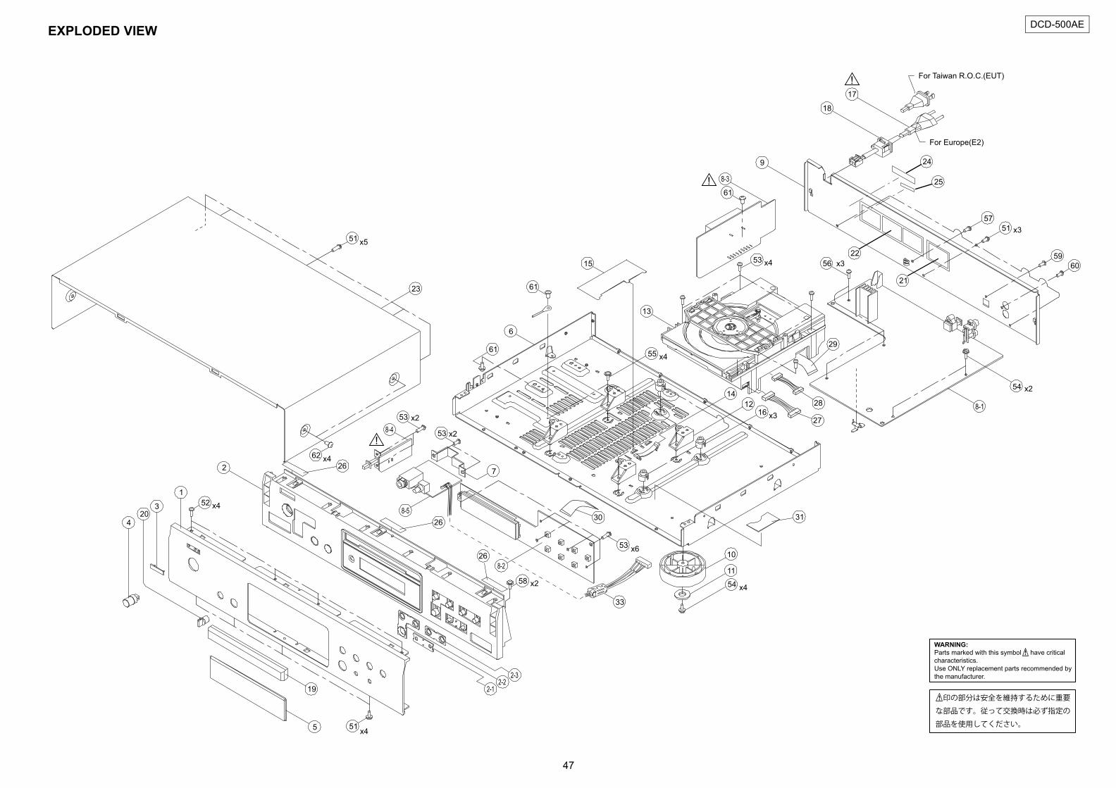
EXPLODED VIEW
Parts marked with this symbol have criticalcharacteristics.Use ONLY replacement parts recommended bythe manufacturer.
WARNING:
印の部分は安全を維持するために重要
な部品です。従って交換時は必ず指定の
部品を使用してください。
48
DCD-500AE
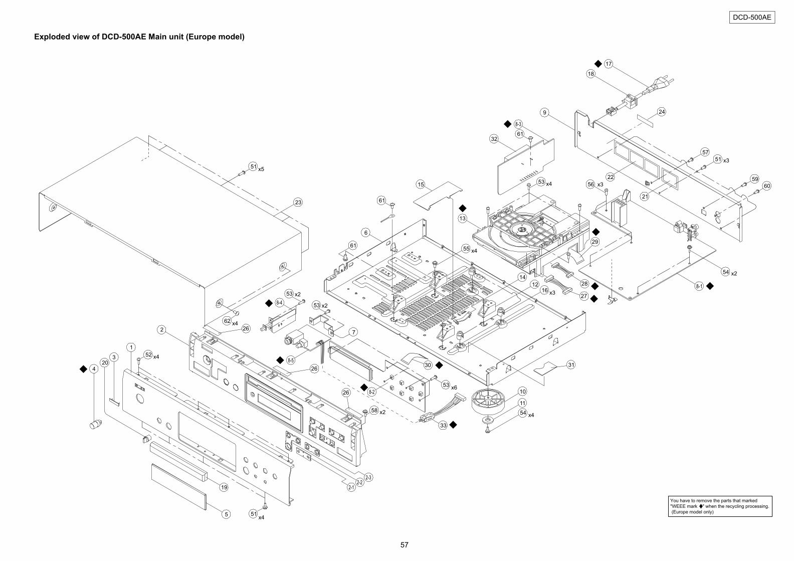
PARTS LIST OF EXPLODED VIEW*本表に記載されている部品は、補修用部品のため製品に使用している部品とは一部、形状、寸法などが異なる場合があります。* The parts listed below are for maintenance only, might differ from the parts used in the unit in appearances or dimensions.
* "nsp" 印の部品は常時在庫していませんので供給に長時間を要することがあります。場合によっては、供給をお断りする場合があります。* Part indicated with the mark “nsp” are not always in stock and possibly to take a long period of time for supplying, or in some case supplying of part may be refused.
Note: The symbols in the column "Remarks" indicate the following destinations.BKE2 : Europe model(Black) SPE2 : Europe model(Premium Silver) EUT : Taiwan R.O.C. model(Premium Silver)
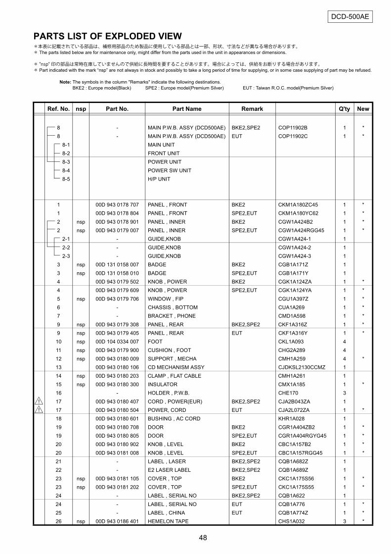
Ref. No. nsp Part No. Part Name Remark Q'ty New
8 - MAIN P.W.B. ASSY (DCD500AE) BKE2,SPE2 COP11902B 1 *8 - MAIN P.W.B. ASSY (DCD500AE) EUT COP11902C 1 *
8-1 MAIN UNIT8-2 FRONT UNIT8-3 POWER UNIT8-4 POWER SW UNIT8-5 H/P UNIT
1 00D 943 0178 707 PANEL , FRONT BKE2 CKM1A180ZC45 1 *1 00D 943 0178 804 PANEL , FRONT SPE2,EUT CKM1A180YC62 1 *2 nsp 00D 943 0178 901 PANEL , INNER BKE2 CGW1A424B2 1 *2 nsp 00D 943 0179 007 PANEL , INNER SPE2,EUT CGW1A424RGG45 1 *
2-1 - GUIDE,KNOB CGW1A424-1 12-2 - GUIDE,KNOB CGW1A424-2 12-3 - GUIDE,KNOB CGW1A424-3 1
3 nsp 00D 131 0158 007 BADGE BKE2 CGB1A171Z 13 nsp 00D 131 0158 010 BADGE SPE2,EUT CGB1A171Y 14 00D 943 0179 502 KNOB , POWER BKE2 CGK1A124ZA 1 *4 00D 943 0179 609 KNOB , POWER SPE2,EUT CGK1A124YA 1 *5 nsp 00D 943 0179 706 WINDOW , FIP CGU1A397Z 1 *6 - CHASSIS , BOTTOM CUA1A269 1 *7 - BRACKET , PHONE CMD1A598 1 *9 nsp 00D 943 0179 308 PANEL , REAR BKE2,SPE2 CKF1A316Z 1 *9 nsp 00D 943 0179 405 PANEL , REAR EUT CKF1A316Y 1 *10 nsp 00D 104 0334 007 FOOT CKL1A093 411 nsp 00D 943 0179 900 CUSHION , FOOT CHG2A289 412 nsp 00D 943 0180 009 SUPPORT , MECHA CMH1A259 4 *13 00D 943 0180 106 CD MECHANISM ASSY CJDKSL2130CCMZ 114 nsp 00D 943 0180 203 CLAMP , FLAT CABLE CMH1A261 115 nsp 00D 943 0180 300 INSULATOR CMX1A185 1 *16 - HOLDER , P.W.B. CHE170 3
! 17 00D 943 0180 407 CORD , POWER(EUR) BKE2,SPE2 CJA2B043ZA 1! 17 00D 943 0180 504 POWER, CORD EUT CJA2L072ZA 1 *
18 00D 943 0180 601 BUSHING , AC CORD KHR1A028 119 00D 943 0180 708 DOOR BKE2 CGR1A404ZB2 1 *19 00D 943 0180 805 DOOR SPE2,EUT CGR1A404RGYG45 1 *20 00D 943 0180 902 KNOB , LEVEL BKE2 CBC1A157B2 1 *20 00D 943 0181 008 KNOB , LEVEL SPE2,EUT CBC1A157RGG45 1 *21 - LABEL , LASER BKE2,SPE2 CQB1A682Z 122 - E2 LASER LABEL BKE2,SPE2 CQB1A689Z 123 nsp 00D 943 0181 105 COVER , TOP BKE2 CKC1A175S56 1 *23 nsp 00D 943 0181 202 COVER , TOP SPE2,EUT CKC1A175S55 1 *24 - LABEL , SERIAL NO BKE2,SPE2 CQB1A622 124 - LABEL , SERIAL NO EUT CQB1A776 1 *25 - LABEL , CHINA EUT CQB1A774Z 1 *26 nsp 00D 943 0186 401 HEMELON TAPE CHS1A032 3 *
49
DCD-500AE
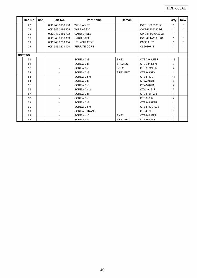
27 00D 943 0186 508 WIRE ASS'Y CWB1B005080EG 1 *28 00D 943 0186 605 WIRE ASS'Y CWB5A906080EG 1 *29 00D 943 0186 702 CARD CABLE CWC4F1A16A220B 1 *30 00D 943 0186 809 CARD CABLE CWC4F4A11A100A 1 *31 00D 943 0200 904 HT INSULATOR CMX1A187 1 *33 00D 943 0201 000 FERRITE CORE CLZ9Z071Z 1 *
SCREWS51 - SCREW 3x8 BKE2 CTBD3+8JFZR 1251 - SCREW 3x8 SPE2,EUT CTBD3+8JFN 952 - SCREW 3x8 BKE2 CTB3+8GFZR 452 - SCREW 3x8 SPE2,EUT CTB3+8GFN 453 - SCREW 3x10 CTB3+10GR 1454 - SCREW 3x8 CTW3+8JR 655 - SCREW 3x6 CTW3+6JR 456 - SCREW 3x12 CTW3+12JR 357 - SCREW 3x6 CTB3+6FFZR 158 - SCREW 3x8 CTB3+8JR 259 - SCREW 3x8 CTB3+8GFZR 160 - SCREW 3x10 CTB3+10GFZR 161 - SCREW , TRANS CTB4+6FR 362 - SCREW 4x6 BKE2 CTB4+6JFZR 462 - SCREW 4x6 SPE2,EUT CTB4+6JFN 4
Ref. No. nsp Part No. Part Name Remark Q'ty New
50
DCD-500AE
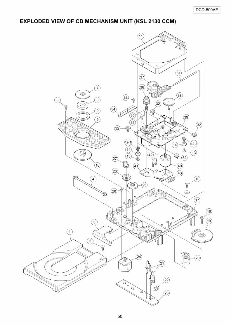
EXPLODED VIEW OF CD MECHANISM UNIT (KSL 2130 CCM)
�
� � � �� � � �
� �
� �
� �
� �
� �
� �
� �
� �
� �
� �
�
�
�
� �
� �
� �
� �
� �
� �
� �
� �
� �
� �
� �
�
� �
� �
�
� �
�
� �
�
� �
�
�
� �
� �
� �
� �
�
� �
� �
�
51
DCD-500AE
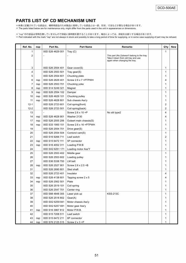
PARTS LIST OF CD MECHANISM UNIT*本表に記載されている部品は、補修用部品のため製品に使用している部品とは一部、形状、寸法などが異なる場合があります。* The parts listed below are for maintenance only, might differ from the parts used in the unit in appearances or dimensions.
* "nsp" 印の部品は常時在庫していませんので供給に長時間を要することがあります。場合によっては、供給をお断りする場合があります。* Part indicated with the mark “nsp” are not always in stock and possibly to take a long period of time for supplying, or in some case supplying of part may be refused.
Ref. No. nsp Part No. Part Name Remarks Q'ty New
1 00D S26 4629 001 Tray (C) 12 - - This part (No.2)doesn't belong to the tray.
Take it down from old tray and use again when changing the tray.
3 00D S26 2554 401 Gear cover(S) 14 00D S26 2553 501 Tray gear(S) 15 00D S26 2554 601 Chucking plate 16 nsp 00D S26 2629 401 Screw 2.6 x 7 +PTPWH 47 nsp 00D S26 2553 701 Chucking yoke 18 nsp 00D S14 5249 321 Magnet 19 nsp 00D S26 2554 102 Damper 1
10 nsp 00D S26 4629 101 Chucking pulley 111 nsp 00D S26 4628 801 Sub chassis Ass'y 1
12-1 00D S26 2723 601 Coil spring(front) 2 12-2 00D S26 2723 501 Coil spring(back) 2
13 - Screw 2.6 x 10 +P No slit type2 414 nsp 00D S26 4628 901 Washer 2130 417 nsp 00D S26 2555 206 Outsert main chassis(S) 118 nsp 00D S33 1950 151 Screw 2.6 x 16 +PTPWH 119 00D S26 2554 701 Drive gear(S) 120 00D S26 2554 504 Contorol cam(S) 121 00D S16 9266 711 Leaf switch 222 nsp 00D S15 6472 111 5P connector 123 nsp 00D S16 4052 311 Loading P.W.B 124 00D SX2 6251 171 Loading motor Ass'Y 125 00D S26 2553 402 Middle gear 126 00D S26 2553 602 Loading pulley 127 00D S36 5338 700 LM belt 128 nsp 00D S26 2527 901 Screw 2.6 x 2.5 +B 131 00D S26 2690 801 Sled shaft 132 00D S26 2723 401 Insulator 433 nsp 00D S26 4138 601 Tapping screw 2 x 5 434 nsp 00D S26 2562 501 Plate 135 00D S26 2519 101 Coil spring 136 00D S26 2547 701 Center ring 137 00D S88 4848 305 Laser pick up KSS-213C 138 00D S26 2518 802 Gear(A) 139 00D SX2 6259 841 Motor chassis Ass'y 140 00D SX2 6257 691 Motor gear Ass'y 141 nsp 00D S16 3967 812 Motor P.W.B. 142 00D S15 7208 511 Leaf switch 143 nsp 00D S15 6472 211 6P connector 144 nsp 00D S76 2125 515 Screw 2 x 3 +P 1
52
DCD-500AE
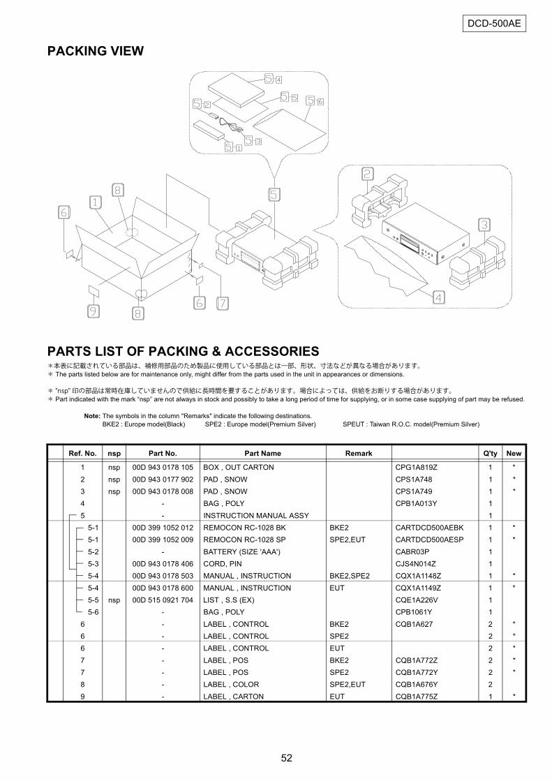
PACKING VIEW
PARTS LIST OF PACKING & ACCESSORIES*本表に記載されている部品は、補修用部品のため製品に使用している部品とは一部、形状、寸法などが異なる場合があります。* The parts listed below are for maintenance only, might differ from the parts used in the unit in appearances or dimensions.
* "nsp" 印の部品は常時在庫していませんので供給に長時間を要することがあります。場合によっては、供給をお断りする場合があります。* Part indicated with the mark “nsp” are not always in stock and possibly to take a long period of time for supplying, or in some case supplying of part may be refused.
Note: The symbols in the column "Remarks" indicate the following destinations.BKE2 : Europe model(Black) SPE2 : Europe model(Premium Silver) SPEUT : Taiwan R.O.C. model(Premium Silver)
Ref. No. nsp Part No. Part Name Remark Q'ty New
1 nsp 00D 943 0178 105 BOX , OUT CARTON CPG1A819Z 1 *2 nsp 00D 943 0177 902 PAD , SNOW CPS1A748 1 *3 nsp 00D 943 0178 008 PAD , SNOW CPS1A749 1 *4 - BAG , POLY CPB1A013Y 15 - INSTRUCTION MANUAL ASSY 1
5-1 00D 399 1052 012 REMOCON RC-1028 BK BKE2 CARTDCD500AEBK 1 *5-1 00D 399 1052 009 REMOCON RC-1028 SP SPE2,EUT CARTDCD500AESP 1 *5-2 - BATTERY (SIZE 'AAA') CABR03P 15-3 00D 943 0178 406 CORD, PIN CJS4N014Z 15-4 00D 943 0178 503 MANUAL , INSTRUCTION BKE2,SPE2 CQX1A1148Z 1 *5-4 00D 943 0178 600 MANUAL , INSTRUCTION EUT CQX1A1149Z 1 *5-5 nsp 00D 515 0921 704 LIST , S.S (EX) CQE1A226V 15-6 - BAG , POLY CPB1061Y 1
6 - LABEL , CONTROL BKE2 CQB1A627 2 *6 - LABEL , CONTROL SPE2 2 *6 - LABEL , CONTROL EUT 2 *7 - LABEL , POS BKE2 CQB1A772Z 2 *7 - LABEL , POS SPE2 CQB1A772Y 2 *8 - LABEL , COLOR SPE2,EUT CQB1A676Y 29 - LABEL , CARTON EUT CQB1A775Z 1 *
53
DCD-500AE
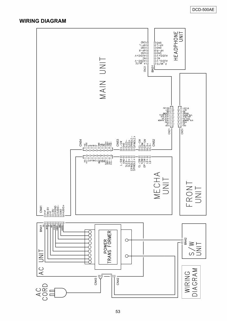
WIRING DIAGRAM
BN41
CN41
CN43
CN54
CN53
CN52
BN31
CN42
BN42
54
DCD-500AE
NOTE FOR SCHEMATIC DIAGRAM
WARNING:Parts marked with this symbol ! have critical characteristics.Use ONLY replacement parts recommended by the manufactur-er.
CAUTION:Before returning the unit to the customer, make sure you make either (1) a leakage current check or (2) a line to chassis resis-tance check. If the leakage current exceeds 0.5 milliamps, or if the resistance from chassis to either side of the power cord is less than 460 kohms, the unit is defective.
WARNING:DO NOT return the unit to the customer until the problem is lo-cated and corrected.
NOTICE:ALL RESISTANCE VALUES IN OHM. k=1,000 OHMM=1,000,000 OHMALL CAPACITANCE VALUES IN MICRO FARAD.P=MICRO-MICRO FARADEACH VOLTAGE AND CURRENT ARE MEASURED ATNO SIGNAL INPUT CONDITION.CIRCUIT AND PARTS ARE SUBJECT TO CHANGEWITHOUT PRIOR NOTICE.
配線図について
! 印の部品は安全を維持するために重要な部品です。従って交換時は必ず指定の部品を使用してください。
注)(1) 指定なき抵抗値はΩ、kはkΩ、MはMΩを示す。
(2) 指定なきコンデンサーの値は µF、pはpFを示す。(3) 各部の電圧は無信号の値を示す。
(4) この配線図は基本配線図です。改良等のため変更することがありますのでご了承ください。
55
AVR-1906 / AVR-786 / AVC-1620
SIGNAL LINE
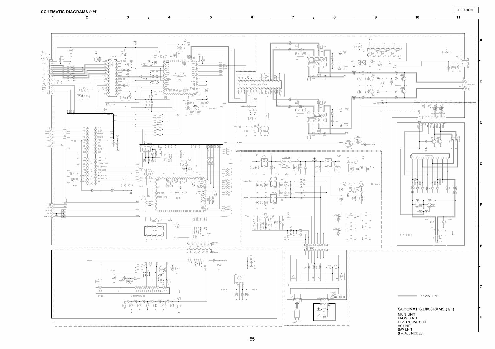
SCHEMATIC DIAGRAMS (1/1)
MAIN UNIT
FRONT UNIT
HEADPHONE UNIT
AC UNIT
S/W UNIT
(For ALL MODEL)
SCHEMATIC DIAGRAMS (1/1)
1 2 3 4 5 6 7 8 9 10 11
A
B
C
D
E
F
G
H
DCD-500AE
56
DCD-500AE
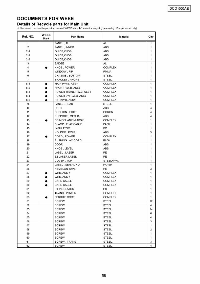
DOCUMENTS FOR WEEEDetails of Recycle parts for Main Unit* You have to remove the parts that marked “WEEE Mark ◆ ” when the recycling processing. (Europe model only)
Ref. NO. WEEEMark Part Name Material Q'ty
1 PANEL , AL AL 12 PANEL , INNER ABS 1
2-1 GUIDE,KNOB ABS 12-2 GUIDE,KNOB ABS 12-3 GUIDE,KNOB ABS 13 BADGE AL 14 ◆ KNOB , POWER COMPLEX 15 WINDOW , FIP PMMA 16 CHASSIS , BOTTOM STEEL. 17 BRACKET , PHONE STEEL. 1
8-1 ◆ MAIN P.W.B. ASSY COMPLEX 18-2 ◆ FRONT P.W.B. ASSY COMPLEX 18-3 ◆ POWER TRANS P.W.B. ASSY COMPLEX 18-4 ◆ POWER SW P.W.B. ASSY COMPLEX 18-5 ◆ H/P P.W.B. ASSY COMPLEX 19 PANEL , REAR STEEL. 1
10 FOOT ABS 411 CUSHION , FOOT PORON 412 SUPPORT , MECHA ABS 413 ◆ CD MECHANISM ASSY COMPLEX 114 CLAMP , FLAT CABLE PA66 115 INSULATOR PC 116 HOLDER , P.W.B. ABS 317 ◆ CORD , POWER COMPLEX 118 BUSHING , AC CORD PA66 119 DOOR ABS 120 KNOB , LEVEL ABS 121 LABEL , LASER PE 122 E2 LASER LABEL PE 123 COVER , TOP STEEL+PVC 124 LABEL , SERIAL NO PAPER 126 HEMELON TAPE PE 327 ◆ WIRE ASS'Y COMPLEX 128 ◆ WIRE ASS'Y COMPLEX 129 ◆ CARD CABLE COMPLEX 130 ◆ CARD CABLE COMPLEX 131 HT INSULATOR PC 132 TRANS , POWER COMPLEX 133 ◆ FERRITE CORE COMPLEX 151 SCREW STEEL. 1252 SCREW STEEL. 453 SCREW STEEL. 1454 SCREW STEEL. 655 SCREW STEEL. 456 SCREW STEEL. 357 SCREW STEEL. 158 SCREW STEEL. 259 SCREW STEEL. 160 SCREW STEEL. 161 SCREW , TRANS STEEL. 362 SCREW STEEL. 4
57
DCD-500AE
Exploded view of DCD-500AE Main unit (Europe model)
1
3
4
2
5
6
7
8-1
8-2
8-3
8-4
8-5
9
21
22
24
10
11
12
14
13
15
16
17
18
19
20
2-12-2
2-3
23
51x4
51 x5
52 x4
53
33
x6
53
53 x2
x2
53 x4
x3
54 x458 x2
54 x2
55 x4
56 x3
57
51 x3
59
60
61
61
62 x4
26
26
26
29
28
27
30 31
61
32
You have to remove the parts that marked
"WEEE mark " when the recycling processing.
(Europe model only)
58
DCD-500AE
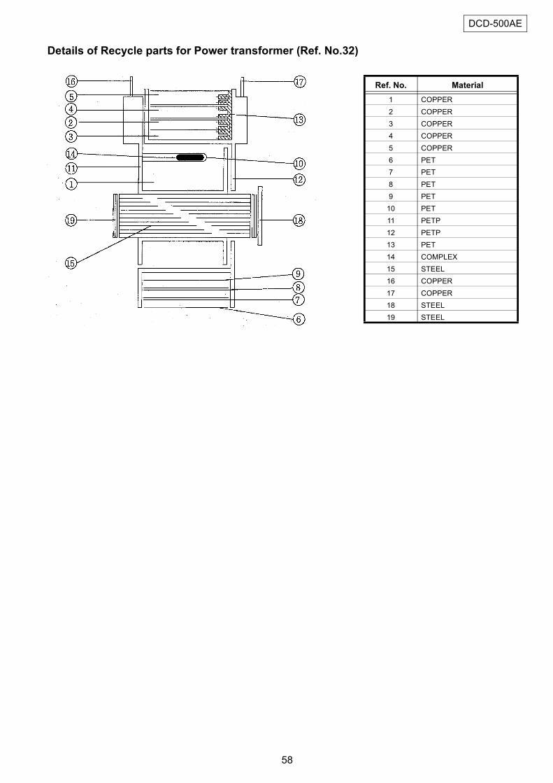
Details of Recycle parts for Power transformer (Ref. No.32)
Ref. No. Material1 COPPER2 COPPER3 COPPER4 COPPER5 COPPER6 PET7 PET8 PET9 PET
10 PET11 PETP12 PETP13 PET14 COMPLEX15 STEEL16 COPPER17 COPPER18 STEEL19 STEEL
Related Documents