VT 2004/5; Micro and Nano- Processing Technologies Ch.14 : Epitaxial Growth Micro and Nano- Processing Technologies EPITAXIAL GROWTH Mahdad Sadeghi [email protected] 031-7721902

Welcome message from author
This document is posted to help you gain knowledge. Please leave a comment to let me know what you think about it! Share it to your friends and learn new things together.
Transcript

VT 2004/5; Micro and Nano-Processing Technologies
Ch.14 : Epitaxial Growth
Micro and Nano- Processing Technologies
EPITAXIAL GROWTH
Mahdad [email protected]
031-7721902

VT 2004/5; Micro and Nano-Processing Technologies
Ch.14 : Epitaxial Growth
CONTROLOFThicknessCompositionThroughput (growth rate)UniformitiyDoping concentrationJunctions(X-tal) Quality, defectsReproducibility
BYGrowth temperatureGas flow rate- FlowmeterSource temperatureFlux cutoff – valves/shuttersX-tal orientationGeometry/ EnvironmentSource/Gas purityPrecleaning
Epitaxy is a well-controlled phase transitionwhich leads to a (single crystalline) solid.

VT 2004/5; Micro and Nano-Processing Technologies
Ch.14 : Epitaxial Growth
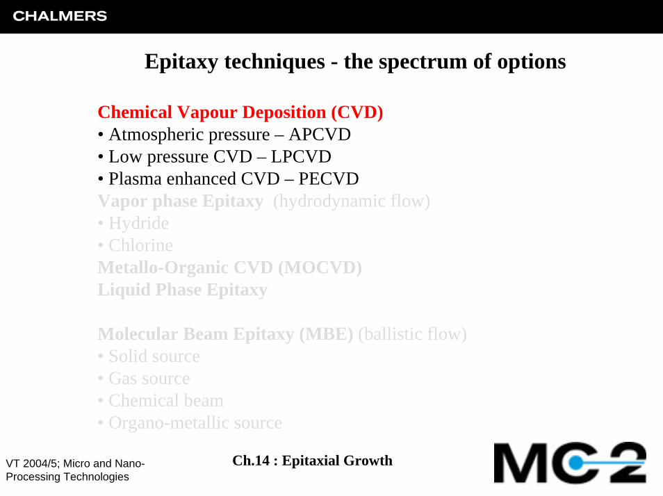
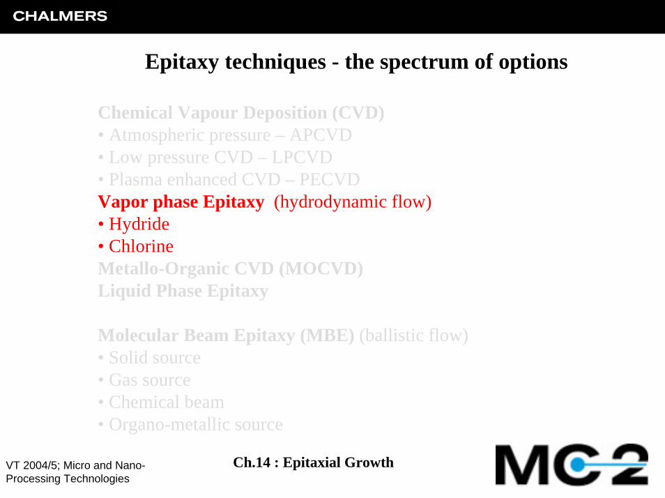
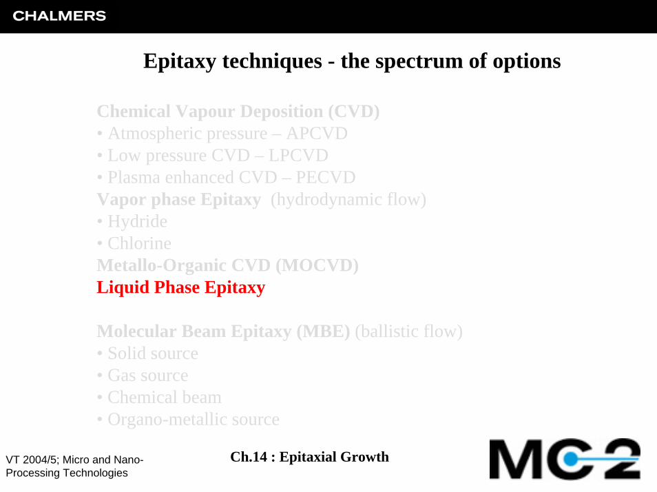
Epitaxy techniques - the spectrum of options
Chemical Vapour Deposition (CVD)• Atmospheric pressure – APCVD• Low pressure CVD – LPCVD• Plasma enhanced CVD – PECVDVapor phase Epitaxy (hydrodynamic flow)• Hydride• Chlorine Metallo-Organic CVD (MOCVD)Liquid Phase Epitaxy
Molecular Beam Epitaxy (MBE) (ballistic flow)• Solid source• Gas source• Chemical beam• Organo-metallic source
VT 2004/5; Micro and Nano-Processing Technologies
Ch.14 : Epitaxial Growth
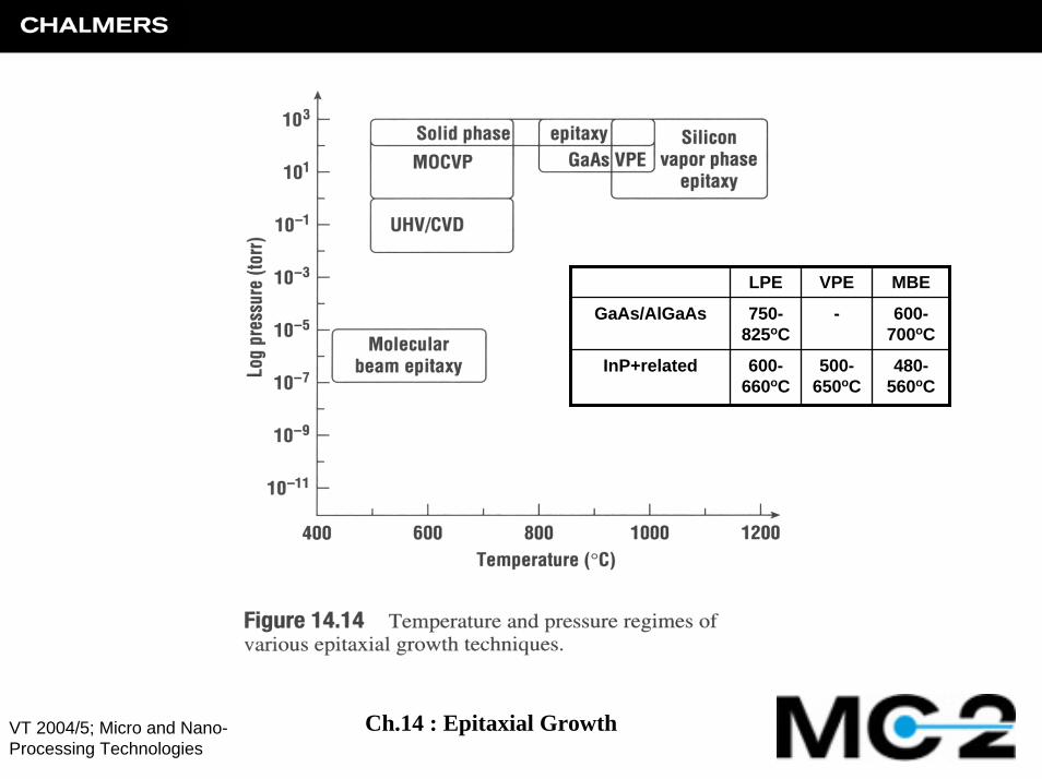
LPE VPE MBE
GaAs/AlGaAs 750-825oC
- 600-700oC
InP+related 600-660oC
500-650oC
480-560oC
VT 2004/5; Micro and Nano-Processing Technologies
Ch.14 : Epitaxial Growth
Epitaxy techniques - the spectrum of options
Chemical Vapour Deposition (CVD)• Atmospheric pressure – APCVD• Low pressure CVD – LPCVD• Plasma enhanced CVD – PECVDVapor phase Epitaxy (hydrodynamic flow)• Hydride• ChlorineMetallo-Organic CVD (MOCVD)Liquid Phase Epitaxy
Molecular Beam Epitaxy (MBE) (ballistic flow)• Solid source• Gas source• Chemical beam• Organo-metallic source

VT 2004/5; Micro and Nano-Processing Technologies
Ch.14 : Epitaxial Growth
CVD Applications
• Thin insulating filmsoxides, silicon nitride
• Polysilicon (gates/conductors)• Epitaxial silicon (single crystal on wafer)• Silicide materials• III-V compounds
VT 2004/5; Micro and Nano-Processing Technologies
Ch.14 : Epitaxial Growth
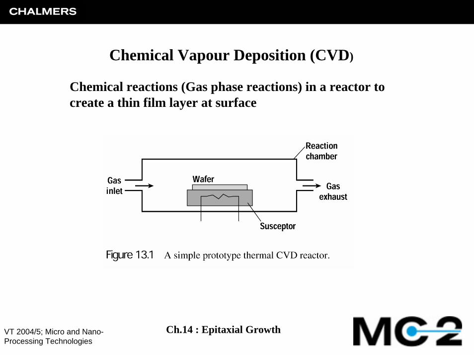
Chemical Vapour Deposition (CVD)
Chemical reactions (Gas phase reactions) in a reactor to create a thin film layer at surface
VT 2004/5; Micro and Nano-Processing Technologies
Ch.14 : Epitaxial Growth
CVD Important film parameters
• Stoichiometery: exact composition of film• Physical parameters: hardness, optical density• Electrical parameters:
dielectric constant, breakdown voltage• Purity of film: lack of contamination• Thickness and uniformity• Conformality and step coverage• pin hole and particle free• Adhesion

VT 2004/5; Micro and Nano-Processing Technologies
Ch.14 : Epitaxial Growth
Four main CVD Reactions• Pyrolysis: heat driven break down• Reduction: usually react with Hydrogen• Oxidation: react with oxygen to form oxides• Nitradation: create nitrides with nitrogen compounds
VT 2004/5; Micro and Nano-Processing Technologies
Ch.14 : Epitaxial Growth
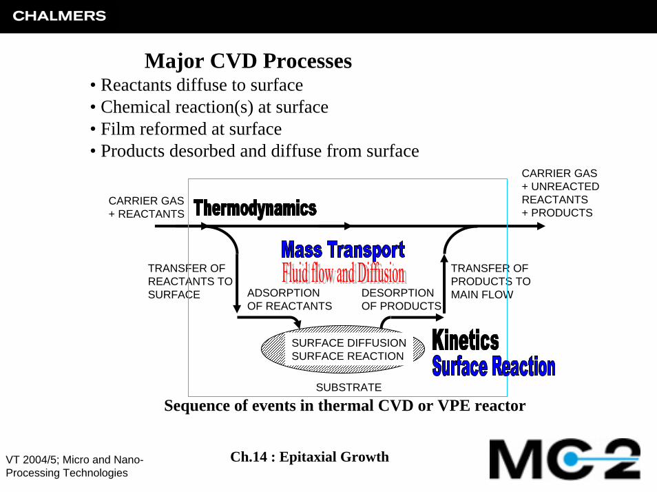
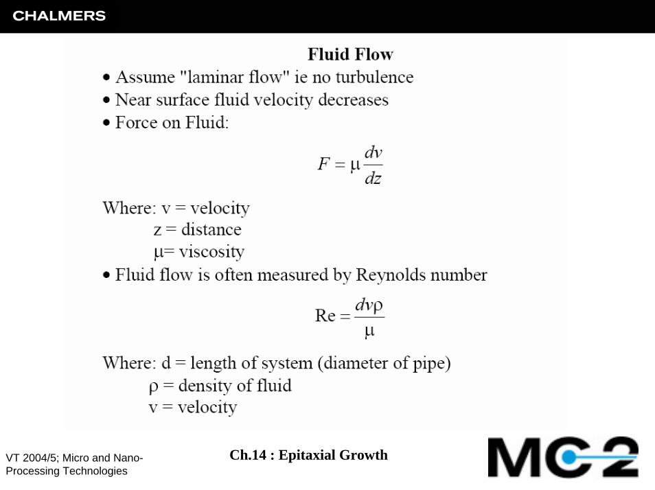
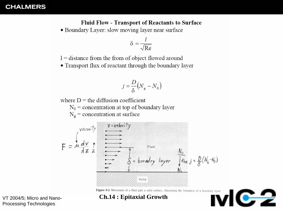
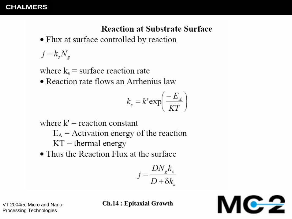
Major CVD Processes• Reactants diffuse to surface• Chemical reaction(s) at surface• Film reformed at surface• Products desorbed and diffuse from surface
CARRIER GAS+ UNREACTED REACTANTS+ PRODUCTS
SUBSTRATE
TRANSFER OFREACTANTS TOSURFACE ADSORPTION
OF REACTANTS DESORPTION OF PRODUCTS
TRANSFER OFPRODUCTS TOMAIN FLOW
CARRIER GAS+ REACTANTS
SURFACE DIFFUSIONSURFACE REACTION
Sequence of events in thermal CVD or VPE reactor
VT 2004/5; Micro and Nano-Processing Technologies
Ch.14 : Epitaxial Growth
VT 2004/5; Micro and Nano-Processing Technologies
Ch.14 : Epitaxial Growth
VT 2004/5; Micro and Nano-Processing Technologies
Ch.14 : Epitaxial Growth

VT 2004/5; Micro and Nano-Processing Technologies
Ch.14 : Epitaxial Growth

VT 2004/5; Micro and Nano-Processing Technologies
Ch.14 : Epitaxial Growth

VT 2004/5; Micro and Nano-Processing Technologies
Ch.14 : Epitaxial Growth
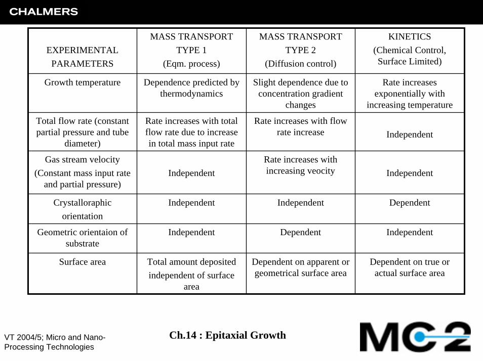
TYPE OF CONTROL RATE LIMITING STEPS
MASS TRANSFERTYPE 1
Inpu Rate LimitedEquilibrium Process
Input rate of reactants to epitaxial growth region
MASS TRANSFERTYPE 2
Diffusion ControlledMass Transfer Limited
Transfer of reactants or products between maingas streaqm and sbstrate
surface by physicalprocesses such as
diffusion or convection
Kinetics ControlSurface Limited
Chemically Controlled
Adsorption of reactantsDesorption of products
Surface reactionSite incorporation
After D.W. Shaw, Mechanisms in Vapour Phase epitaxy of Semiconducors, Crystal Growth Vol1, Ed. C.H.L. Goodman, Plenum press, NY, 174
VT 2004/5; Micro and Nano-Processing Technologies
Ch.14 : Epitaxial Growth
EXPERIMENTALPARAMETERS
MASS TRANSPORTTYPE 1
(Eqm. process)
MASS TRANSPORTTYPE 2
(Diffusion control)
KINETICS(Chemical Control, Surface Limited)
Growth temperature Dependence predicted by thermodynamics
Slight dependence due to concentration gradient
changes
Rate increasesexponentially with
increasing temperature
Total flow rate (constantpartial pressure and tube
diameter)
Rate increases with total flow rate due to increasein total mass input rate
Rate increases with flowrate increase Independent
Gas stream velocity(Constant mass input rate
and partial pressure)Independent
Rate increases with increasing veocity Independent
Crystalloraphicorientation
Independent Independent Dependent
Geometric orientaion of substrate
Independent Dependent Independent
Surface area Total amount depositedindependent of surface
area
Dependent on apparent or geometrical surface area
Dependent on true or actual surface area

VT 2004/5; Micro and Nano-Processing Technologies
Ch.14 : Epitaxial Growth
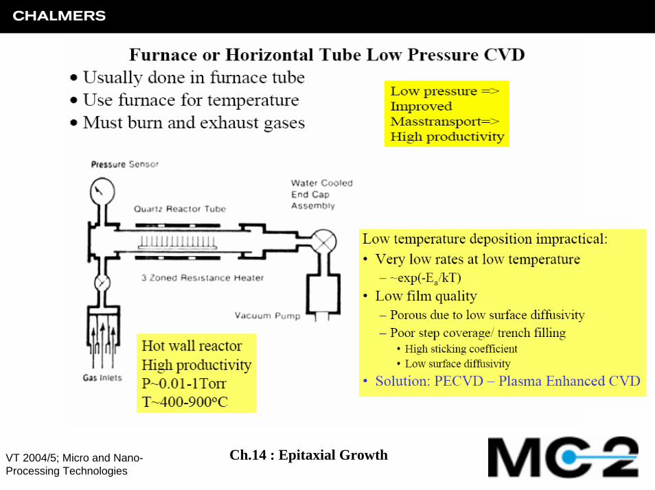
Atmospheric & Low Pressure CVD
Atmospheric Pressure Low pressure
Cold wallHorizontalVerticalPancake
Hot wallPhotochemicalVPEMOCVD
Hot wallPlasma enhancedVertical isothermal
Overview of CVD systems
VPE: Vapour Phase Epitaxy (Si single crystal)MOCVD: Metalo-organic CVD (III-V compounds)

VT 2004/5; Micro and Nano-Processing Technologies
Ch.14 : Epitaxial Growth

VT 2004/5; Micro and Nano-Processing Technologies
Ch.14 : Epitaxial Growth
VT 2004/5; Micro and Nano-Processing Technologies
Ch.14 : Epitaxial Growth
VT 2004/5; Micro and Nano-Processing Technologies
Ch.14 : Epitaxial Growth

VT 2004/5; Micro and Nano-Processing Technologies
Ch.14 : Epitaxial Growth
Plasma Enhanced CVD (PECVD)

VT 2004/5; Micro and Nano-Processing Technologies
Ch.14 : Epitaxial Growth
VT 2004/5; Micro and Nano-Processing Technologies
Ch.14 : Epitaxial Growth
Epitaxy techniques - the spectrum of options
Chemical Vapour Deposition (CVD)• Atmospheric pressure – APCVD• Low pressure CVD – LPCVD• Plasma enhanced CVD – PECVDVapor phase Epitaxy (hydrodynamic flow)• Hydride• Chlorine Metallo-Organic CVD (MOCVD)Liquid Phase Epitaxy
Molecular Beam Epitaxy (MBE) (ballistic flow)• Solid source• Gas source• Chemical beam• Organo-metallic source

VT 2004/5; Micro and Nano-Processing Technologies
Ch.14 : Epitaxial Growth
Vapour Phase Epitaxy (VPE)A process used for depositing thin films on monocrystallinesubstrates using gases.

VT 2004/5; Micro and Nano-Processing Technologies
Ch.14 : Epitaxial Growth
VAPOUR PHASE EPITAXY of III-V materials
Hydride VAPOUR PHASE EPITAXY(HVPE) for depositing GaInAsP
III-sources: InCl and GaClV-sources: PH3 and AsH3 (hydrides of phosphorus and arsenic)
Chloride VAPOUR PHASE EPITAXY (Cl-VPE) for depositing GaInAsP
III-sources: InCl and GaClV-sources: PCl3 and AsCl3 (chlorides of phosphorus and arsenic)
EXAMPLE: InP can be deposited using phosphine and indium chloride gases:
InCl (g) + PH3 (g) = InP (s) + HCl (g) + H2 (g)

VT 2004/5; Micro and Nano-Processing Technologies
Ch.14 : Epitaxial Growth
Hydride VPE
Advantages:+ Purity+ High growth rate+ Throughput+ Versatile for selective growth
Disadvantages:- No Al or Sb alloys- Complex process/reactions- Difficult to control thin layer- Hazardous gases
VT 2004/5; Micro and Nano-Processing Technologies
Ch.14 : Epitaxial Growth
Epitaxy techniques - the spectrum of options
Chemical Vapour Deposition (CVD)• Atmospheric pressure – APCVD• Low pressure CVD – LPCVD• Plasma enhanced CVD – PECVDVapor phase Epitaxy (hydrodynamic flow)• Hydride• Chlorine Metallo-Organic CVD (MOCVD)Liquid Phase Epitaxy
Molecular Beam Epitaxy (MBE) (ballistic flow)• Solid source• Gas source• Chemical beam• Organo-metallic source
VT 2004/5; Micro and Nano-Processing Technologies
Ch.14 : Epitaxial Growth
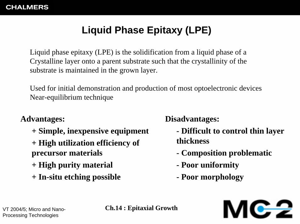
Liquid Phase Epitaxy (LPE)
Liquid phase epitaxy (LPE) is the solidification from a liquid phase of aCrystalline layer onto a parent substrate such that the crystallinity of the substrate is maintained in the grown layer.
Used for initial demonstration and production of most optoelectronic devicesNear-equilibrium technique
Advantages:+ Simple, inexpensive equipment+ High utilization efficiency of precursor materials+ High purity material+ In-situ etching possible
Disadvantages:- Difficult to control thin layerthickness- Composition problematic- Poor uniformity- Poor morphology

VT 2004/5; Micro and Nano-Processing Technologies
Ch.14 : Epitaxial Growth
LPE Growth Procedure
GaAs LPE introducted by H. Nelson (1963)
1) Heat to T>Tsat(saturation temperature)2) Lower T and introduction of seed crystal (Tipper, Dipper, Slider …)3) Withdraw of the sample from the melt
Growth rate will depend on:- Composition of solution- Degree of supersaturation- Cooling rate- Contact period- Subsrate orientation

VT 2004/5; Micro and Nano-Processing Technologies
Ch.14 : Epitaxial Growth
VT 2004/5; Micro and Nano-Processing Technologies
Ch.14 : Epitaxial Growth
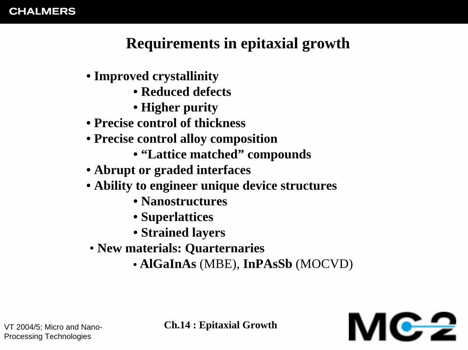
Requirements in epitaxial growth
• Improved crystallinity• Reduced defects• Higher purity
• Precise control of thickness• Precise control alloy composition
• “Lattice matched” compounds• Abrupt or graded interfaces• Ability to engineer unique device structures
• Nanostructures• Superlattices• Strained layers
• New materials: Quarternaries• AlGaInAs (MBE), InPAsSb (MOCVD)

VT 2004/5; Micro and Nano-Processing Technologies
Ch.14 : Epitaxial Growth
How accurate is the control needed?
• Source temperature: < 0.2 deg • In/Ga ratio control in InGaAs < 1 % to avoid dislocations
• 1.5 mm InGaAs/InGaAsP QW (l=±10 nm)Control of QW thickness < 6 %Control of Comp. InGaAs < 0.5 %
• Bragg mirrors thickness control < 1 % mm

VT 2004/5; Micro and Nano-Processing Technologies
Ch.14 : Epitaxial Growth
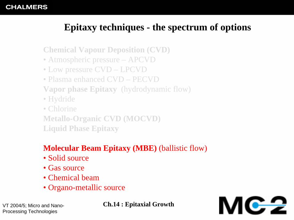
Epitaxy techniques - the spectrum of options
Chemical Vapour Deposition (CVD)• Atmospheric pressure – APCVD• Low pressure CVD – LPCVD• Plasma enhanced CVD – PECVDVapor phase Epitaxy (hydrodynamic flow)• Hydride• Chlorine Metallo-Organic CVD (MOCVD)Liquid Phase Epitaxy
Molecular Beam Epitaxy (MBE) (ballistic flow)• Solid source• Gas source• Chemical beam• Organo-metallic source
VT 2004/5; Micro and Nano-Processing Technologies
Ch.14 : Epitaxial Growth
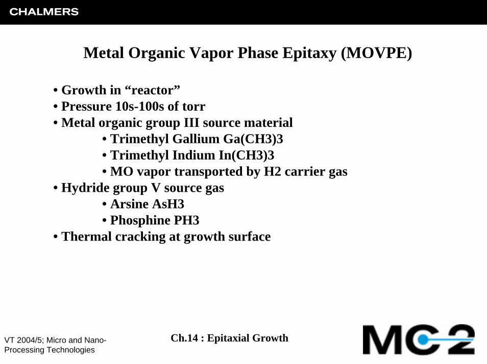
Metal Organic Vapor Phase Epitaxy (MOVPE)
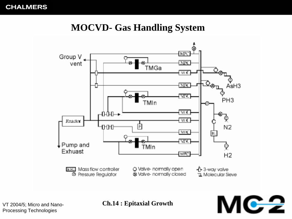
• Growth in “reactor”• Pressure 10s-100s of torr• Metal organic group III source material
• Trimethyl Gallium Ga(CH3)3• Trimethyl Indium In(CH3)3• MO vapor transported by H2 carrier gas
• Hydride group V source gas• Arsine AsH3• Phosphine PH3
• Thermal cracking at growth surface

VT 2004/5; Micro and Nano-Processing Technologies
Ch.14 : Epitaxial Growth
MOCVD- Surface Chemistry

VT 2004/5; Micro and Nano-Processing Technologies
Ch.14 : Epitaxial Growth
Example: OMCVD growth of GaN and related materials
Special problems for GaNand related materials.• No suitable substrate• Difficult to obtain p-typeepilayer
Ga(CH3)3+NH3 GaN+3 CH4
VT 2004/5; Micro and Nano-Processing Technologies
Ch.14 : Epitaxial Growth
MOCVD- Gas Handling System
VT 2004/5; Micro and Nano-Processing Technologies
Ch.14 : Epitaxial Growth
MOCVD Summary
• Growth rates 2-100 micron/hr• high throughput
• P-type doping• Zn (Diethyl Zinc), high diffusivity• C (CCl4, CBr4), amphoteric
• Complex growth kinetics• Delicate interaction between injected gasses, temperatures
• High background pressure• Parasitic incorporation• Intermixing of atoms at interfaces
VT 2004/5; Micro and Nano-Processing Technologies
Ch.14 : Epitaxial Growth
Epitaxy techniques - the spectrum of options
Chemical Vapour Deposition (CVD)• Atmospheric pressure – APCVD• Low pressure CVD – LPCVD• Plasma enhanced CVD – PECVDVapor phase Epitaxy (hydrodynamic flow)• Hydride• Chlorine Metallo-Organic CVD (MOCVD)Liquid Phase Epitaxy
Molecular Beam Epitaxy (MBE) (ballistic flow)• Solid source• Gas source• Chemical beam• Organo-metallic source
VT 2004/5; Micro and Nano-Processing Technologies
Ch.14 : Epitaxial Growth
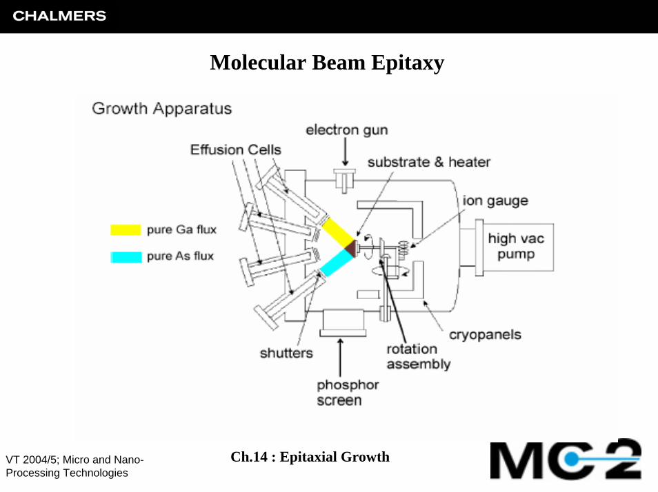
Molecular Beam Epitaxy (MBE)Cho, JVST 8, s31 (1971)
• Homo-epitaxy and heteroepitaxy of semiconductor and compounds• Growth rate: 1µm/hr• Growth in high vacuum chamber
• Ultimate vacuum < 10e-10 torr• Pressure during growth < 10e-6 torr
• Elemental source material• High purity Ga, In, As (99.9999%)• Sources individually evaporated in high temperature cells
• In situ monitoring, calibration• Probing of surface structure during growth• Real time feedback of growth rate

VT 2004/5; Micro and Nano-Processing Technologies
Ch.14 : Epitaxial Growth
Molecular Beam Epitaxy (MBE)
Variations• SSMBE solid evaporation sources• GSMBE metals + group V hydrides• MOMBE metalorganics + conventiona grop Vs• CBE all gas sources

VT 2004/5; Micro and Nano-Processing Technologies
Ch.14 : Epitaxial Growth
MBE Growth Mechanism
- Absorption to the surface,- Surface migration - Incorporation into the crystal lattice - Thermal desorption
VT 2004/5; Micro and Nano-Processing Technologies
Ch.14 : Epitaxial Growth
Molecular Beam Epitaxy

VT 2004/5; Micro and Nano-Processing Technologies
Ch.14 : Epitaxial Growth
MBE- EPI930 System

VT 2004/5; Micro and Nano-Processing Technologies
Ch.14 : Epitaxial Growth
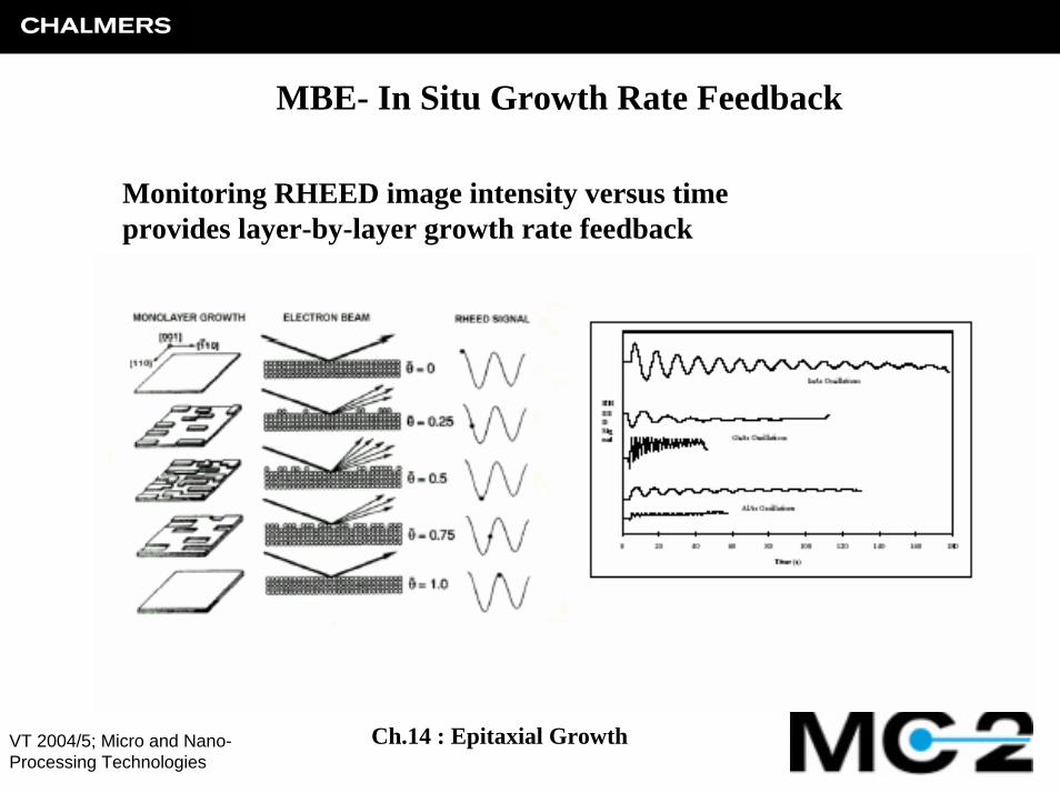
MBE- In Situ Surface Analysis
• High energy (10-30 keV) electron beam• Reflection High Energy Electron Diffraction (RHEED)• Shallow angle of incidence• Beam reconstruction on phosphor screen
VT 2004/5; Micro and Nano-Processing Technologies
Ch.14 : Epitaxial Growth
MBE- In Situ Growth Rate Feedback
Monitoring RHEED image intensity versus timeprovides layer-by-layer growth rate feedback

VT 2004/5; Micro and Nano-Processing Technologies
Ch.14 : Epitaxial Growth
MBE- Summary
• Ultra high vacuum, high purity layers• No chemical byproducts created at growth surface• High uniformity (< 1% deviation)• Growth rates 0.1-10 micron/hr.• High control of composition• In situ monitoring and feedback• Mature production technology
Low P large mean free path beam nature of flux (molecular flow)Mechanical shutters fast switching abrupt interface
Low T limited interdiffusion

VT 2004/5; Micro and Nano-Processing Technologies
Ch.14 : Epitaxial Growth
Gas Source MBE
• Combines advantages of MBE with gas sourcedelivery of group V atoms (as used in MOCVD)
• PH3, AsH3 used for group V sources• Thermally cracked at injector into P2, As2 and H2• P2, As2 dimers arrive at growth surface along with Ga, In• MBE surface kinetics maintained

VT 2004/5; Micro and Nano-Processing Technologies
Ch.14 : Epitaxial Growth
Gas Source MBE
• Advantages of GSMBE• More abrupt junctions than in SSMBE• PH3 a more mature method for phosphorus MBE growth• Improved dynamic range of switching state
• As, P molecules travel around shutter in solid source MBE• Increased control of As/P ratio by adjustment of gas flow• Can replenish group V source material without breaking
vacuum
• Disadvantages• Requires gas handling system• Requires extra vacuum pumping to remove hydrogen• Arsine and Phosphine highly toxic
VT 2004/5; Micro and Nano-Processing Technologies
Ch.14 : Epitaxial Growth
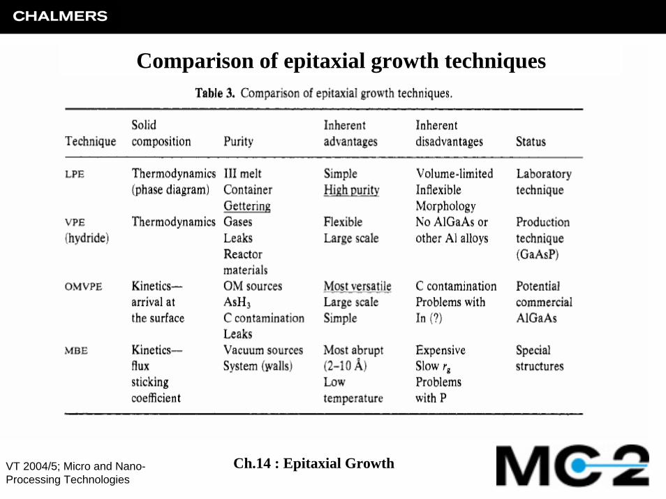
Comparison of epitaxial growth techniques

VT 2004/5; Micro and Nano-Processing Technologies
Ch.14 : Epitaxial Growth
III-V Compound Semiconductors

VT 2004/5; Micro and Nano-Processing Technologies
Ch.14 : Epitaxial Growth
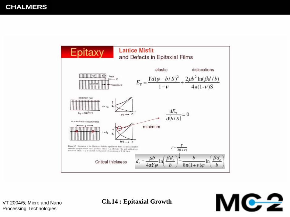
Limits to Strained Layers: Critical Thickness
VT 2004/5; Micro and Nano-Processing Technologies
Ch.14 : Epitaxial Growth

VT 2004/5; Micro and Nano-Processing Technologies
Ch.14 : Epitaxial Growth
VT 2004/5; Micro and Nano-Processing Technologies
Ch.14 : Epitaxial Growth
Related Documents