Mobile System Considerations for SDRAM Interface Trends Andrew B. Kahng †‡ , Vaishnav Srinivas ‡¥ June 5 th , 2011 CSE † and ECE ‡ Departments University of California, San Diego Qualcomm Inc. ¥

Mobile System Considerations for SDRAM Interface Trends Andrew B. Kahng †‡, Vaishnav Srinivas ‡¥ June 5 th, 2011 CSE † and ECE ‡ Departments University.
Dec 21, 2015
Welcome message from author
This document is posted to help you gain knowledge. Please leave a comment to let me know what you think about it! Share it to your friends and learn new things together.
Transcript

Mobile System Considerations for SDRAM Interface Trends
Andrew B. Kahng†‡, Vaishnav Srinivas‡¥
June 5th, 2011
CSE† and ECE‡ DepartmentsUniversity of California, San Diego
Qualcomm Inc. ¥

(2/13)
Outline
• SDRAM Memory Interfaces: Today and Tomorrow
• Motivation
• Trends in DRAM Density and Data Rate
• Trends in Mobile Processor Requirements
• Memory Interface Calculator
• Exploration Using the Calculator
• Summary and Next Steps

(3/13)
SDRAM Memory Interfaces Today and Tomorrow
• Various interconnect and signaling options exist:
o Interconnect:
Die stack/MCP POP DIMM 3D-Stack
o Signaling:
DDR, XDR, Serial, Wide IO
• Exploration of these options based on the primary bounds (Capacity, Throughput, Power and Latency) is required for making the correct tradeoffs
(4/13)
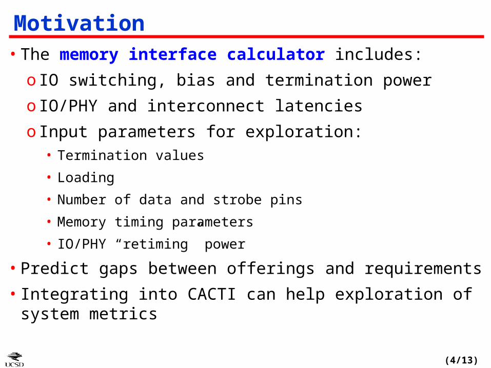
Motivation• The memory interface calculator includes:
o IO switching, bias and termination power
o IO/PHY and interconnect latencies
o Input parameters for exploration:• Termination values
• Loading
• Number of data and strobe pins
• Memory timing parameters
• IO/PHY “retiming” power
• Predict gaps between offerings and requirements
• Integrating into CACTI can help exploration of system metrics
(5/13)
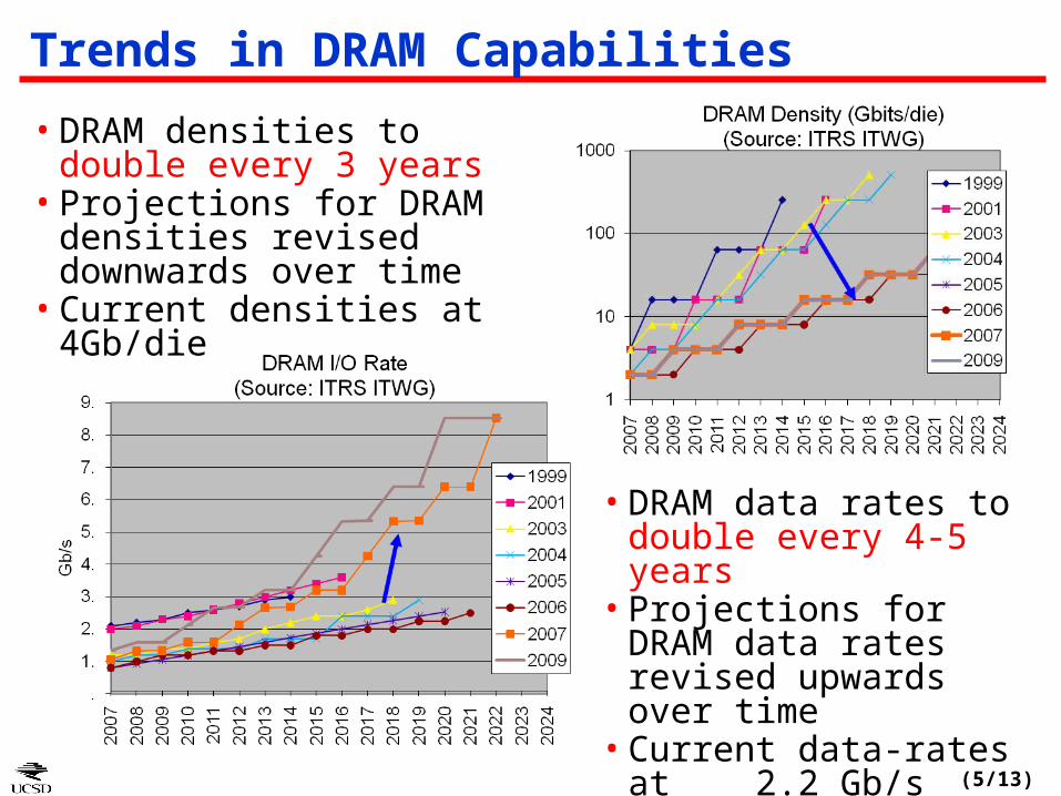
Trends in DRAM Capabilities
• DRAM densities to double every 3 years
• Projections for DRAM densities revised downwards over time
• Current densities at 4Gb/die
• DRAM data rates to double every 4-5 years
• Projections for DRAM data rates revised upwards over time
• Current data-rates at 2.2 Gb/s

(6/13)
Trends in Mobile Processor Requirements
Market 2010 2011 2012 2013 2014
Desktop 3.0 4.2 5.6 7.4 10.2
Laptop 2.0 3.3 4.6 6.3 8.0
Mobile 0.3 0.5 0.8 1.0 1.3
• Trends for mobile processor requirements
oCapacity to scale 3-4x every 3 years
oThroughput to double every 3 years
• The requirements are very dynamic!
• Quick exploration and projection for compatible memories is useful
Capacity Requirements in GB(Source: IDC)
Mobile Handset Throughput Requirements in GB/s(Source: Qualcomm)
(7/13)
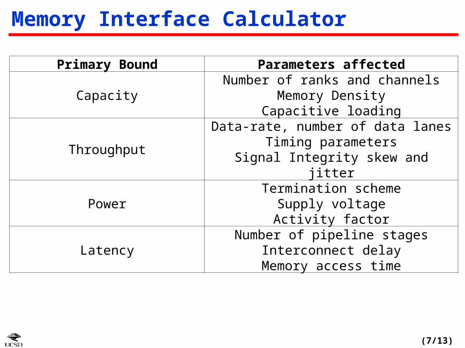
Memory Interface Calculator
Primary Bound Parameters affected
CapacityNumber of ranks and channels
Memory DensityCapacitive loading
ThroughputData-rate, number of data lanes
Timing parametersSignal Integrity skew and jitter
PowerTermination scheme
Supply voltageActivity factor
LatencyNumber of pipeline stages
Interconnect delayMemory access time

(8/13)
Memory Interface Calculator Summary
Bound LPDDR2 TSS-Wide IO DDR3 Serial Mobile-XDR
Clock Speed (MHz) 300-533,
DDR 200-333, SDR 400-800, DDR 4-8 GHz, Serial 400-533, Octal
Throughput (GB/s) 3-4.3 12-24 6-13 12-17 12-17
Peak IO Power Efficiency (mW/GBps)
~40 ~10 ~120 ~60 ~20
Peak Core Power Efficiency (mW/GBps)
~50 ~35 ~100 ~50 ~50
Total Peak Power Efficiency (mW/GBps)
~90 ~45 ~220 ~110 ~70
Active Idle IO Power (mW) ~6-10 ~2-4 ~500-600 ~450 ~200
Active Idle Core Power (mW) ~20 ~20 ~150 ~20 ~20
Capacity (GB) (Current trends)
0.5-1 for x32
dual rank
0.5-2 through multi-die stacking
2-8 for dual-rank
DIMM
0.5-1 for x32 dual rank
0.5-1 for x32 dual rank
Latency from MC-DRAM-MC ~50ns ~40ns
~45ns, but penalty if DLL
is off (~512 Tck)
~65ns, PLL lock penalty if off
~60ns, DLL penalty if off

(9/13)
Memory Interface Calculator Summary
Throughput in GB/s
• The spider chart highlights the design space coveredo Wide IO covers the largest space
for lower capacitieso Large capacity systems still need
DDR3/DDR4• Alternatives to be explored outside
the existing space?
• Before LPDDR3 came up in JEDEC, Wide-IO and Serial Memory were being explored.
• LPDDR3 was brought up as a way to fill this gap in 2012-2014 timeframe

(10/13)
Exploration using the calculator• How fast can LPDDR3 operate?
o With terminations?o With DLL/better retiming?o With lower loading?o With better packaging?o POP versus MCP
• Wide IO exploration?o Transition to DDR for Wide IO?o Number of data lanes per strobe – 8, 16 or 32?o When does interface timing and signal/power integrity become an issue
for Wide IO?
• High-capacity memory alternatives to DDR3/DDR4?o MCP with larger number of wire-bonded dies?o TSS with large number of stacks (8?)o TSS-MCP if stacking with processor is a thermal risk?

(11/13)
LPDDR3 Exploration
Inputs to the calculator Value Units
Number of memories on data pin 1
Number of memories on add pin 1
Number of memories on clk pin 1
Frequency of clock 1250 MHz
Retiming current 25 mA
Number of data pins 32
Number of DQS pairs 8
Termination RTT on DQ & DQS 60 ohms
Termination RTT on CA 60 ohms
Memory density for each memory core 4 Gb
TDS 100 ps
TDH 100 ps
TDQSQ 100 ps
TQHS 100 ps
Outputs of the calculator Value Units
Signal Swing on DQ&DQS, Vsw.DQ 0.80 (V)
Switching Power on DQ 52.80 (mW)
Switching Power on DQS 52.80 (mW)
Switching Power on CLK + CLK diff termination 12.78 (mW)
Bias and Static Power 30.00 (mW)
Signal Swing on CA, Vsw.DQ 0.65 (V)
Switching Power on CA 19.24 (mW)
Termination Power 225.45 (mW)
I/O power for CPU chip 393.07 (mW)
Throughput 10 GB/s
Capacity 0.5 GB
Latency 38.6 ns
Tskew 41 ps
Tjitter 29 ps
Terror 20 ps
Timing margin WRITE 60 ps
Timing margin READ -5 ps

(12/13)
LPDDR3 Exploration
Maximum speeds for: Preliminary Answers from the calculator
POP, Unterminated LPDDR3 with ~150ps memory timing parameters (tDS/tDH/tDQSQ/tQHS)?
800MHz for single-rank 800MHz for dual-rank will need careful architecture
and design
POP, Terminated LPDDR3 with ~100ps memory timing parameters? 1250MHz
External (MCP), Unterminated LPDDR3Even 533MHz for dual-rank is
challenging and may need sophisticated retiming
External (MCP), Terminated LPDDR3? 1066MHz
(13/13)
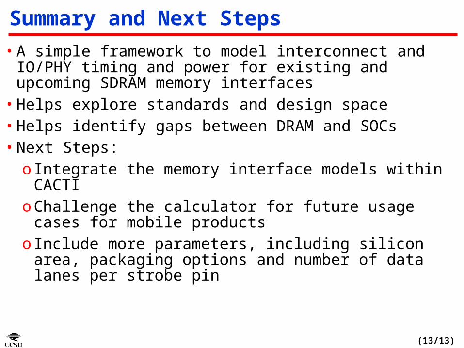
Summary and Next Steps
• A simple framework to model interconnect and IO/PHY timing and power for existing and upcoming SDRAM memory interfaces
• Helps explore standards and design space• Helps identify gaps between DRAM and SOCs• Next Steps:o Integrate the memory interface models within CACTI oChallenge the calculator for future usage cases for mobile
productso Include more parameters, including silicon area, packaging
options and number of data lanes per strobe pin
Related Documents