DSP HARDWARE 7.a SECTION 7 DSP HARDWARE ■ Microcontrollers, Microprocessors, and Digital Signal Processors (DSPs) ■ DSP Requirements ■ ADSP-21xx 16-Bit Fixed-Point DSP Core ■ Fixed-Point Versus Floating Point ■ ADI SHARC® Floating Point DSPs ■ ADSP-2116x Single-Instruction, Multiple Data (SIMD) Core Architecture ■ TigerSHARC™: The ADSP-TS001 Static Superscalar DSP ■ DSP Benchmarks ■ DSP Evaluation and Development Tools

Welcome message from author
This document is posted to help you gain knowledge. Please leave a comment to let me know what you think about it! Share it to your friends and learn new things together.
Transcript

DSP HARDWARE
7.a
SECTION 7
DSP HARDWARE
� Microcontrollers, Microprocessors, and Digital SignalProcessors (DSPs)
� DSP Requirements
� ADSP-21xx 16-Bit Fixed-Point DSP Core
� Fixed-Point Versus Floating Point
� ADI SHARC® Floating Point DSPs
� ADSP-2116x Single-Instruction, Multiple Data (SIMD)Core Architecture
� TigerSHARC™: The ADSP-TS001Static Superscalar DSP
� DSP Benchmarks
� DSP Evaluation and Development Tools

DSP HARDWARE
7.b

DSP HARDWARE
7.1
SECTION 7DSP HARDWAREDan King, Greg Geerling, Ken Waurin, NoamLevine, Jesse Morris, Walt Kester
MICROCONTROLLERS, MICROPROCESSORS, ANDDIGITAL SIGNAL PROCESSORS (DSPS)Computers are extremely capable in two broad areas: (1) data manipulation, suchas word processing and database management, and (2) mathematical calculation,used in science, engineering, and Digital Signal Processing. However, mostcomputers are not optimized to perform both functions. In computing applicationssuch as word processing, data must be stored, sorted, compared, moved, etc., andthe time to execute a particular instruction is not critical, as long as the program’soverall response time to various commands and operations is adequate enough tosatisfy the end user. Occasionally, mathematical operations may also be performed,as in a spreadsheet or database program, but speed of execution is generally not thegoverning factor. In most general purpose computing applications there is noconcentrated attempt by software companies to make the code efficient. Applicationprograms are loaded with “features” which require more memory and fasterprocessors with every new release or upgrade.
Figure 7.1
On the other hand, digital signal processing applications require that mathematicaloperations be performed quickly, and the time to execute a given instruction mustbe known precisely, and it must be predictable. Both code and hardware must beextremely efficient to accomplish this. As has been shown in the last two sections ofthis book, the most fundamental mathematical operation or kernel in all of DSP is
GENERAL COMPUTING APPLICATIONS
DATA MANIPULATION MATH CALCULATION
� Word Processing� Database Management� Spread Sheets� Operating Systems
� Digital Signal Processing� Motion Control� Engineering Simulations� Real-Time Signal Processing
� Data Movement (A→→→→ B)� Value Testing (If A = B, then…)
� Time to Execute not Critical, not Predictable
� Addition (C = A + B)� Multiplication (C = A × B)
� Time to Execute Critical and Predictable

DSP HARDWARE
7.2
the sum-of-products (or dot-product). Fast execution of the dot product is critical tofast Fourier transforms (FFTs), real time digital filters, matrix multiplications,graphics pixel manipulation, etc.
Based on this introductory discussion of DSP requirements, it is important tounderstand the differences between microcontrollers, microprocessors, and DSPs.While microcontrollers used in industrial process control applications can performfunctions such as multiplication, addition, and division, they are much more suitedto applications where I/O capability and control is more important than speed.Microcontrollers such as the 8051-family typically contain a CPU, RAM, ROM,serial/parallel interfaces, timers, and interrupt circuitry. The MicroConverter™series from Analog Devices contains not only the 8051 core but also highperformance ADC and DAC functions along with flash memory.
Figure 7.2
Microprocessors, such as the Pentium-series from Intel, are basically single-chipCPUs which require additional circuitry to make up the total computing function.Microprocessor instruction sets can be either complex-instruction-set computer(CISC) or reduced-instruction-set computer (RISC). The complex-instruction-setcomputer (CISC) includes instructions for basic processor operations, plus singleinstructions that are highly sophisticated; for example, to evaluate a high-orderpolynomial. But CISC has a price: many of the instructions execute via microcodein the CPU and require numerous clock cycles plus silicon real estate for codestorage memory.
MICROCONTROLLERS, MICROPROCESSORS,AND DIGITAL SIGNAL PROCESSORS (DSPs)
� Microcontrollers:� CPU, RAM, ROM, Serial/Parallel Interface, Timer, Interrupt Circuitry� Well Suited for Toasters as well Industrial Process Control� Speed is not Generally a Requirement!� Compact Instruction Sets� Example: 8051, 68HC11, PIC
� Microprocessors:� Single Chip CPU - Requires Additional External Circuitry� RISC: Reduced Instruction Set Computer� CISC: Complex Instruction Set Computer� Example: Pentium-Series, PowerPC, MIPS
� Digital Signal Processors (DSPs):� RAM, ROM, Serial/Parallel Interface, Interrupt Circuitry� CPU Optimized for Fast Repetitive Math for Real Time Processing� Example: ADSP-21XX, ADSP-21K
DSP HARDWARE
7.3
In contrast, the reduced-instruction-set computer (RISC) recognizes that, in manyapplications, basic instructions such as LOAD and STORE - with simple addressingschemes - are used much more frequently than the advanced instructions, andshould not incur an execution penalty. These simpler instructions are hardwired inthe CPU logic to execute in a single clock cycle, reducing execution time and CPUcomplexity.
Although the RISC approach offers many advantages in general purpose computing,it is not well suited to DSP. For example, most RISCs do not support single-instruction multiplication, a very common and repetitive operation in DSP. TheDSP is optimized to accomplish these tasks fast enough to maintain real-timeoperation in the context of the application. This requires single-cycle arithmeticoperations and accumulations.
DSP REQUIREMENTS
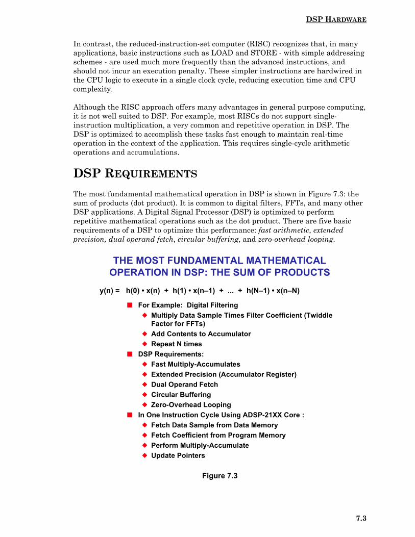
The most fundamental mathematical operation in DSP is shown in Figure 7.3: thesum of products (dot product). It is common to digital filters, FFTs, and many otherDSP applications. A Digital Signal Processor (DSP) is optimized to performrepetitive mathematical operations such as the dot product. There are five basicrequirements of a DSP to optimize this performance: fast arithmetic, extendedprecision, dual operand fetch, circular buffering, and zero-overhead looping.
Figure 7.3
THE MOST FUNDAMENTAL MATHEMATICALOPERATION IN DSP: THE SUM OF PRODUCTS
� For Example: Digital Filtering� Multiply Data Sample Times Filter Coefficient (Twiddle
Factor for FFTs)� Add Contents to Accumulator� Repeat N times
� DSP Requirements:� Fast Multiply-Accumulates� Extended Precision (Accumulator Register)� Dual Operand Fetch� Circular Buffering� Zero-Overhead Looping
� In One Instruction Cycle Using ADSP-21XX Core :� Fetch Data Sample from Data Memory� Fetch Coefficient from Program Memory� Perform Multiply-Accumulate� Update Pointers
y(n) = h(0) • x(n) + h(1) • x(n–1) + ... + h(N–1) • x(n–N)

DSP HARDWARE
7.4
FAST ARITHMETIC
Fast arithmetic is the simplest of these requirements to understand. Since real-timeDSP applications are driven by performance, the multiply-accumulate or MAC timeis a basic requirement; faster MACs mean potentially higher bandwidth. It iscritical to remember that MAC time alone does not define DSP performance. Thisoften forgotten fact leads to an inadequate measure of processor performance bysimply examining its MIPS (million instructions per second) rating. Since most DSPand DSP-like architectures feature MACs that can execute an instruction everycycle, most processors are given a MIPS rating equal to its MAC throughput. Thisdoes not necessarily account for the other factors that can degrade a processorsoverall performance in real-world applications. The other four criteria can wipe outMAC gains if they are not satisfied.
In addition to the requirement for fast arithmetic, a DSP should be able to supportother general purpose math functions and should therefore have an appropriatearithmetic logic unit (ALU) and a programmable shifter function for bitmanipulation.
EXTENDED PRECISION
Apart from the obvious need for fast multiplication and addition (MAC), there isalso a requirement for extended precision in the accumulator register. For example,when two 16-bit words are multiplied, the result is a 32-bit word. The AnalogDevices ADSP-21xx 16-bit fixed-point core architecture has an internal 40-bitaccumulator which provides a high degree of overflow protection. While floating-point DSPs eliminate most of the problems associated with precision and overflow,fixed-point processors are still popular for many applications, and thereforeoverflow, underflow, and data scaling issues must be dealt with properly.
DUAL OPERAND FETCH
Regardless of the nature of a processor, performance limitations are generally basedon bus bandwidth. In the case of general purpose microprocessors ormicrocontrollers, code is dominated by single memory fetch instructions, usuallyaddressed as a base plus offset value. This leads architects to embed fixed data intothe instruction set so that this class of memory access is fast and memory efficient.DSPs, on the other hand, are dominated by instructions requiring two independentmemory fetches. This is driven by the basic form of the convolution (kernel or dotproduct) Σh(i)x(i). The goal of fast dual operand fetches is to keep the MAC fullyloaded. We saw in the discussion on MACs that the performance of a DSP is firstlimited by MAC time. Assuming an adequate MAC cycle time, two data values needto be supplied at the same rate; increases in operand fetch cycle time will result incorresponding increases in MAC cycle time. Ideally, the operand fetches occursimultaneously with the MAC instruction so that the combination of the MAC andmemory addressing occurs in one cycle.
Dual operand fetch is implemented in DSPs by providing separate buses forprogram memory data and data memory data. In addition, separate programmemory address and data memory address buses are also provided. The MAC can

DSP HARDWARE
7.5
therefore receive inputs from each data bus simultaneously. This architecture isoften referred to as the Harvard Architecture.
CIRCULAR BUFFERING
If we examine the kernel equation more carefully, the advantages of circularbuffering in DSP applications become apparent. A Finite Impulse Response (FIR)filter is used to demonstrate the point. First, coefficients or tap values for FIR filtersare periodic in nature. Second, the FIR filter uses the newest real-world signalvalue and discards the oldest value when calculating each output.
In the series of FIR filter equations, the N coefficient locations are always accessedsequentially from h(0) to h(N–1). The associated data points circulate through thememory as follows: new samples are stored replacing the oldest data each time afilter output is computed. A fixed boundary RAM can be used to achieve thiscirculating buffer effect. The oldest data sample is replaced by the newest with eachconvolution. A "time history" of the N most recent samples is kept in RAM.
This delay line can be implemented in fixed boundary RAM in a DSP chip if newdata values are written into memory, overwriting the oldest value. To facilitatememory addressing, old data values are read from memory starting with the valueone location after the value that was just written. In a 4-tap FIR filter, for example,x(4) is written into memory location 0, and data values are then read from locations1, 2, 3, and 0. This example can be expanded to accommodate any number of taps.By addressing data memory locations in this manner, the address generator needonly supply sequential addresses regardless of whether the operation is a memoryread or write. This data memory buffer is called circular because when the lastlocation is reached, the memory pointer must be reset to the beginning of the buffer.
The coefficients are fetched simultaneously with the data. Due to the addressingscheme chosen, the oldest data sample is fetched first. Therefore, the last coefficientmust be fetched first. The coefficients can be stored backwards in memory: h(N–1) isthe first location, and h(0) is the last, with the address generator providingincremental addresses. Alternatively, coefficients can be stored in a normal mannerwith the accessing of coefficients starting at the end of the buffer, and the addressgenerator being decremented.
This allows direct support of the FIR filter unit delay taps without softwareoverhead. These data characteristics are DSP algorithm-specific and must besupported in hardware to achieve the best DSP performance. Implementing circularbuffers in hardware allows buffer parameters (i.e. start, length, etc.) to be set upoutside of the core instruction loop. This eliminates the need for extra instructionswithin the loop body. Lack of a hardware implementation for circular buffering cansignificantly impact MAC performance.
ZERO OVERHEAD LOOPING
Zero overhead looping is required by the repetitive nature of the kernel equation.The multiply-accumulate function and the data fetches required are repeated Ntimes every time the kernel function is calculated. Traditional microprocessors
DSP HARDWARE
7.6
implement loops that have one instruction execution time or more of overheadassociated with repeating the loop. Analog Devices’ DSP architectures providehardware support that eliminates the need for looping instructions within the loopbody. For true DSP architectures, the difference of zero overhead body looping andprogrammed looping can easily exceed 20% cycle time.
SUMMARY
Any processor can accomplish any software task, given enough time. However,DSPs are optimized for the unique computational requirements of real-time, real-world signal processing. Traditional computers are better suited for tasks that canbe performed in non-real-time. In the following section, we will examine thearchitecture of a high-performance 16-bit fixed-point DSP Microcomputer, theAnalog Devices’ ADSP-21xx-family.
ADSP-21XX 16-BIT FIXED-POINT DSP CORE
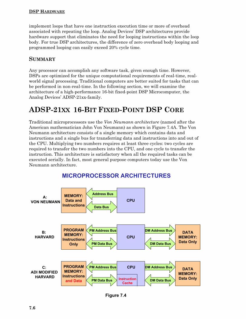
Traditional microprocessors use the Von Neumann architecture (named after theAmerican mathematician John Von Neumann) as shown in Figure 7.4A. The VonNeumann architecture consists of a single memory which contains data andinstructions and a single bus for transferring data and instructions into and out ofthe CPU. Multiplying two numbers requires at least three cycles: two cycles arerequired to transfer the two numbers into the CPU, and one cycle to transfer theinstruction. This architecture is satisfactory when all the required tasks can beexecuted serially. In fact, most general purpose computers today use the VonNeumann architecture.
Figure 7.4
MICROPROCESSOR ARCHITECTURES
MEMORY:Data and
Instructions Data Bus
Address Bus
CPU
PM Data Bus
PM Address Bus
DM Data Bus
DM Address BusPROGRAMMEMORY:
InstructionsOnly
CPUDATA
MEMORY:Data Only
PM Data Bus
PM Address Bus
DM Data Bus
DM Address BusPROGRAMMEMORY:
Instructionsand Data
DATAMEMORY:Data OnlyInstruction
Cache
CPU
A: VON NEUMANN
B: HARVARD
C: ADI MODIFIED
HARVARD

DSP HARDWARE
7.7
For faster processing, however, the Harvard architecture shown in Figure 7.4B ismore suitable. This is named for the work done at Harvard University under theleadership of Howard Aiken. Data and program instructions each have separatememories and buses as shown. Since the buses operate independently, programinstructions and data can be fetched at the same time, thereby improving the speedover the single bus Von Neumann design. In order to perform a single FIR filtermultiply-accumulate, an instruction is fetched from the program memory, andduring the same cycle, a coefficient can be fetched from data memory. A second cycleis required to fetch the data word from the data memory.
Figure 7.4C illustrates Analog Devices’ modified Harvard architecture whereinstructions and data are allowed in the program memory. For example, in the caseof a digital filter, the coefficients are stored in the program memory, and the datasamples in the data memory. A coefficient and a data sample can thus be fetched ina single cycle. In addition to fetching the coefficient from program memory and adata sample from data memory, an instruction must also be fetched from programmemory. Analog Devices’ DSPs handle this in one of two ways. In the first method,the program memory is accessed twice (double pumped) in an instruction cycle. TheADSP-218x series uses this method. In the second method, a program memorycache is provided. If an algorithm requires dual data fetches, the programmer placesone buffer in program memory and the other in data memory. The first time theprocessor executes an instruction, there is a one-cycle stall because it must fetch theinstruction and the coefficient over the program memory data bus. However,whenever this conflict occurs, the DSP “caches” the instruction in a cache memory.The next time this instruction is required, the program sequencer obtains it fromthe cache, while the coefficient is obtained over the program memory data bus. Thecache method if used in the ADSP-219x family as well as in the SHARC family.
DIGITAL FILTER EXAMPLE
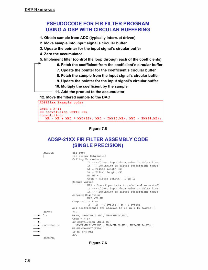
Now that the fundamental architecture of the ADSP-21xx family has beenpresented, a simple FIR filter design will illustrate the ease of programming thefamily. Pseudocode for an FIR filter design is shown in Figure 7.5. For AnalogDevices’ DSPs, all operations within the filter loop are completed in one instructioncycle, thereby greatly increasing efficiency. Extra instructions are not required torepeat the loop. This is referred to as zero-overhead looping. The actual FIR filterassembly code for the ADSP-21xx family of fixed point DSPs is shown in Figure 7.6.The arrows in the diagram point to the actual executable instructions (7 lines), therest of the code are simply comments added for clarification. The first instruction(labeled fir:) sets up the computation by clearing the MR register and loading theMX0 and MY0 registers with the first data and coefficient values from data andprogram memory. The multiply-accumulate with dual data fetch in the convolutionloop is then executed N–1 times in N–1 cycles to compute the sum of the first N–1products. The final multiply-accumulate instruction is performed with the roundingmode enabled to round the result to the upper 24 bits of the MR register. The MR1register is then conditionally saturated to its most positive or negative value basedon the status of the overflow flag contained in the MV register. In this manner,results are accumulated to the full 40-bit precision of the MR register, withsaturation of the output only if the final result overflowed beyond the leastsignificant 32 bits of the MR register.
DSP HARDWARE
7.8
Figure 7.5
Figure 7.6
PSEUDOCODE FOR FIR FILTER PROGRAMUSING A DSP WITH CIRCULAR BUFFERING
1. Obtain sample from ADC (typically interrupt driven)2. Move sample into input signal’s circular buffer3. Update the pointer for the input signal’s circular buffer4. Zero the accumulator5. Implement filter (control the loop through each of the coefficients)
6. Fetch the coefficient from the coefficient’s circular buffer 7. Update the pointer for the coefficient’s circular buffer 8. Fetch the sample from the input signal’s circular buffer 9. Update the pointer for the input signal’s circular buffer10. Multiply the coefficient by the sample11. Add the product to the accumulator
12. Move the filtered sample to the DACADSP21xx Example code:
CNTR = N-1;DO convolution UNTIL CE;convolution: MR = MR + MX0 * MY0(SS), MX0 = DM(I0,M1), MY0 = PM(I4,M5);
ADSP-21XX FIR FILTER ASSEMBLY CODE(SINGLE PRECISION)
.MODULE fir_sub;{ FIR Filter Subroutine
Calling ParametersI0 --> Oldest input data value in delay lineI4 --> Beginning of filter coefficient tableL0 = Filter length (N)L4 = Filter length (N)M1,M5 = 1CNTR = Filter length - 1 (N-1)
Return ValuesMR1 = Sum of products (rounded and saturated)I0 --> Oldest input data value in delay lineI4 --> Beginning of filter coefficient table
Altered RegistersMX0,MY0,MR
Computation Time(N - 1) + 6 cycles = N + 5 cycles
All coefficients are assumed to be in 1.15 format. }
.ENTRY fir;fir: MR=0, MX0=DM(I0,M1), MY0=PM(I4,M5);
CNTR = N-1;DO convolution UNTIL CE;
convolution: MR=MR+MX0*MY0(SS), MX0=DM(I0,M1), MY0=PM(I4,M5);MR=MR+MX0*MY0(RND);IF MV SAT MR;RTS;
.ENDMOD;
DSP HARDWARE
7.9
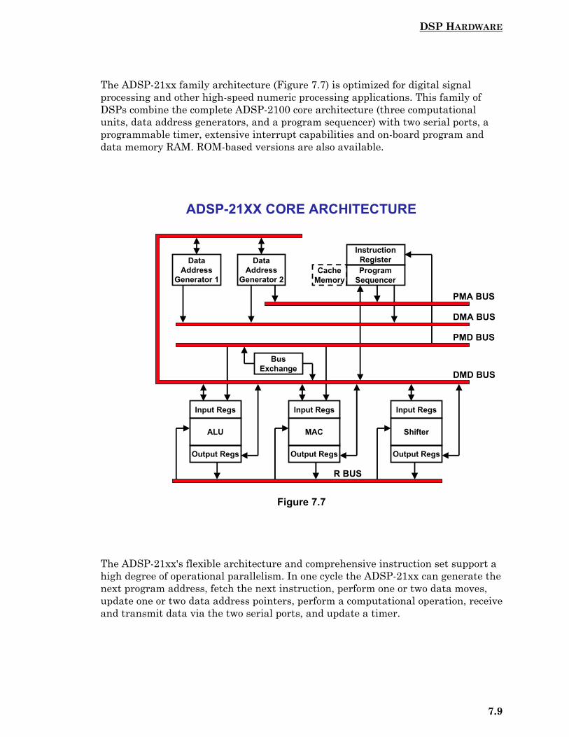
The ADSP-21xx family architecture (Figure 7.7) is optimized for digital signalprocessing and other high-speed numeric processing applications. This family ofDSPs combine the complete ADSP-2100 core architecture (three computationalunits, data address generators, and a program sequencer) with two serial ports, aprogrammable timer, extensive interrupt capabilities and on-board program anddata memory RAM. ROM-based versions are also available.
Figure 7.7
The ADSP-21xx's flexible architecture and comprehensive instruction set support ahigh degree of operational parallelism. In one cycle the ADSP-21xx can generate thenext program address, fetch the next instruction, perform one or two data moves,update one or two data address pointers, perform a computational operation, receiveand transmit data via the two serial ports, and update a timer.
ADSP-21XX CORE ARCHITECTURE
DataAddress
Generator 1
DataAddress
Generator 2
InstructionRegisterProgram
Sequencer
ALU
Input Regs
Output Regs
MAC
Input Regs
Output Regs
Shifter
Input Regs
Output Regs
BusExchange
PMA BUS
DMA BUS
PMD BUS
DMD BUS
R BUS
CacheMemory

DSP HARDWARE
7.10
Figure 7.8
BUSES
The ADSP-21xx processors have five internal buses to ensure efficient data transfer.The program memory address (PMA) and data memory address (DMA) buses areused internally for the addresses associated with program and data memory. Theprogram memory data (PMD) and data memory data (DMD) buses are used for thedata associated with the memory spaces. Off chip, the buses are multiplexed into asingle external address bus and a single external data bus; the address spaces areselected by the appropriate control signals. The result (R) bus transfersintermediate results directly between the various computational units.
The PMA bus is 14-bits wide allowing direct access of up to 16K words of data. Thedata memory data (DMD) bus is 16-bits wide. The DMD bus provides a path for thecontents of any register in the processor to be transferred to any other register or toany data memory location in a single cycle. The data memory address comes fromtwo sources: an absolute value specified in the instruction code (direct addressing)or the output of a data address generator (indirect addressing). Only indirectaddressing is supported for data fetches from program memory.
The program memory data (PMD) bus can also be used to transfer data to and fromthe computational units through direct paths or via the PMD-DMD bus exchangeunit. The PMD-DMD bus exchange unit permits data to be passed from one bus tothe other. It contains hardware to overcome the 8-bit width discrepancy between thetwo buses, when necessary.
ADSP-21XX CORE ARCHITECTURE
� Buses� Program Memory Address (PMA)� Data Memory Address (DMA)� Program Memory Data (PMD)� Data Memory Data (DMD)� Result (R)
� Computational Units� Arithmetic Logic Unit (ALU)� Multiply-Accumulator (MAC)� Shifter
� Data Address Generators� Program Sequencer� On-Chip Peripheral Options
� Program Memory RAM or ROM� Data Memory RAM� Serial Ports� Timer� Host Interface Port� DMA Port

DSP HARDWARE
7.11
Program memory can store both instructions and data, permitting the ADSP-21xxto fetch two data operands in a single cycle, one from program memory and onefrom data memory. The corresponding instruction is obtained directly from programmemory by “double pumping” (ADSP-218x series) or from a cache memory (ADSP-219x and SHARC series).
COMPUTATIONAL UNITS (ALU, MAC, SHIFTER)
The processor contains three independent computational units: the arithmetic logicunit (ALU), the multiplier-accumulator (MAC), and the barrel shifter. Thecomputational units process 16-bit data directly and have provisions to supportmultiprecision computations. The ALU has a carry-in (CI) bit which allows it tosupport 32-bit arithmetic.
The ALU provides a standard set of arithmetic and logic functions: add, subtract,negate, increment, decrement, absolute value, AND, OR, EXCLUSIVE OR andNOT. Two divide primitives are also provided.
Figure 7.9
The MAC performs single-cycle multiply, multiply/add, and multiply/subtractoperations. It also contains a 40-bit accumulator which provides 8-bits of overflow insuccessive additions to ensure that no loss of data occurs; 256 overflows would haveto occur before any data is lost. Special instructions are provided for implementingblock floating-point scaling of data. A set of background registers is also available inthe MAC for interrupt service routines. If after a DSP routine is finished and theMV flag has been set, this means that the register contains a word greater than 32bits. The register can be “saturated” using the saturation routine which normalizesthe 40-bit word to either a negative fullscale or positive fullscale 32-bit word in 1.32format.
ARITHMETIC LOGIC UNIT (ALU) FEATURES
� Add, Subtract, Negate, Increment, Decrement, AbsoluteValue, AND, OR, Exclusive OR, NOT
� Bitwise Operators, Constant Operators
� Multi-Precision Math Capabilites
� Divide Primitives
� Saturation Mode for Overflow Support
� Background Registers for Single-Cycle Context Switch
� Example Instructions:� IF EQ AR = AX0 + AY0;
� AF = MR1 XOR AY1;
� AR = TGLBIT 7 OF AX1;
DSP HARDWARE
7.12
Figure 7.10
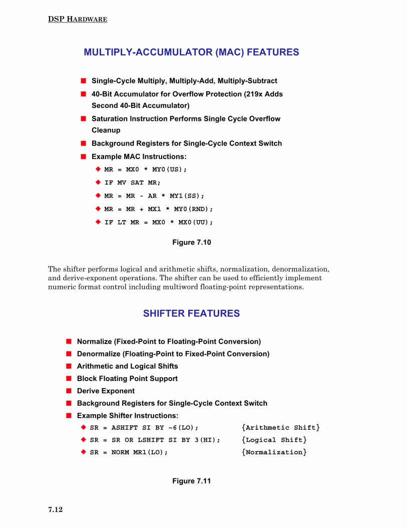
The shifter performs logical and arithmetic shifts, normalization, denormalization,and derive-exponent operations. The shifter can be used to efficiently implementnumeric format control including multiword floating-point representations.
Figure 7.11
MULTIPLY-ACCUMULATOR (MAC) FEATURES
� Single-Cycle Multiply, Multiply-Add, Multiply-Subtract
� 40-Bit Accumulator for Overflow Protection (219x AddsSecond 40-Bit Accumulator)
� Saturation Instruction Performs Single Cycle OverflowCleanup
� Background Registers for Single-Cycle Context Switch
� Example MAC Instructions:� MR = MX0 * MY0(US);
� IF MV SAT MR;
� MR = MR - AR * MY1(SS);
� MR = MR + MX1 * MY0(RND);
� IF LT MR = MX0 * MX0(UU);
SHIFTER FEATURES
� Normalize (Fixed-Point to Floating-Point Conversion)� Denormalize (Floating-Point to Fixed-Point Conversion)� Arithmetic and Logical Shifts� Block Floating Point Support� Derive Exponent� Background Registers for Single-Cycle Context Switch� Example Shifter Instructions:
� SR = ASHIFT SI BY –6(LO); {Arithmetic Shift}
� SR = SR OR LSHIFT SI BY 3(HI); {Logical Shift}
� SR = NORM MR1(LO); {Normalization}

DSP HARDWARE
7.13
The computational units are arranged side-by-side instead of serially so that theoutput of any unit may be the input of any unit on the next cycle. The internalresult (R) bus directly connects the computational units to make this possible.
DATA ADDRESS GENERATORS AND PROGRAM SEQUENCER
Two dedicated data address generators and a powerful program sequencer ensureefficient use of the computational units. The data address generators (DAGs)provide memory addresses when memory data is transferred to or from the input oroutput registers. Each DAG keeps track of up to four address pointers. Wheneverthe pointer is used to access data (indirect addressing), it is post-modified by thevalue of a specified modify register. A length value may be associated with eachpointer to implement automatic modulo addressing for circular buffers. With twoindependent DAGs, the processor can generate two addresses simultaneously fordual operand fetches.
DAG1 can supply addresses to data memory only; DAG2 can supply addresses toeither data memory or program memory. When the appropriate mode bit is set inthe mode status register (MSTAT), the output address of DAG1 is bit-reversedbefore being driven onto the address bus. This feature facilitates addressing inradix-2 FFT algorithms.
Figure 7.12
DATA ADDRESS GENERATOR FEATURES
� Automatic Linear Addressing and Circular Buffering� Each DAG Manages Four Pointers� Supports Dual Operand Fetch� Bit-Reverser (DAG1) For FFTs� Background Registers in ADSP-219x� Example DAG Instructions:
� AX0 = DM(I0,M3);
� MODIFY(I1,M2);
� MR = MR + MX0 * MY0, MX0 = DM(I0,M1), MY0 = PM(I4,M4);
Fetch Data Memory Data Word Located at Address I0, Increment Pointer by M1
Fetch Program Memory Data Word Located at Address I4, Increment Pointer by M4

DSP HARDWARE
7.14
The program sequencer supplies instruction addresses to the program memory. Thesequencer is driven by the instruction register which holds the currently executinginstruction. The instruction register introduces a single level of pipelining into theprogram flow. Instructions are fetched and loaded into the instruction registerduring one processor cycle, and executed during the following cycle while the nextinstruction is prefetched. To minimize overhead cycles, the sequencer supportsconditional jumps, subroutine calls and returns in a single cycle. With an internalloop counter and loop stack, the processor executes looped code with zero overhead.No explicit jump instructions are required to loop. The sequencer also efficientlyprocesses interrupts with its interrupt controller for fast interrupt response withminimum latency. When an interrupt occurs, it causes a jump to a known specifiedlocation in memory. Short interrupt service routines can be coded in place. Forinterrupt service routines with more than four instructions, program control istransferred to the service routine by means of a JUMP instruction placed at theinterrupt vector location.
Figure 7.13
ADSP-21XX-FAMILY ON-CHIP PERIPHERALS
The discussion so far has involved the core architecture of the fixed-point ADSP-21xx DSPs which is common to all members of the family. This section discusses theon-chip peripherals which have different configurations and options depending onthe particular processor in the family. The ADSP-218x architecture is shown inFigure 7.14.
PROGRAM SEQUENCER FEATURES
� Generates Next Instruction Address� Low-Latency Interrupt Handling� Hardware Stacks� Single-Cycle Conditional Branch (218x)� Supports Zero-Overhead Looping
ADSP21xx Example code:
CNTR = 10;DO endloop UNTIL CE; IO(DACCONTROL) = AX0; MR = MR + MX0 * MY0(SS), MX0 = DM(I0,M1), MY0 = PM(I4,M5);endloop: IF MV SET FL1; IF EQ CALL mysubroutine;

DSP HARDWARE
7.15
Figure 7.14
Figure 7.15
EXTERNALADDRESS
BUS
ADSP-218x FAMILY ARCHITECTURE
PROGRAMSEQUENCER
DATA ADDRESSGENERATORS
ARITHMETIC UNITS
POWERDOWNCONTROL
MEMORY
BYTE DMACONTROLLER
SERIAL PORTS
PROGRAMMABLEEXTERNAL I / Oand FLAG PINS
EXTERNALDATA BUS
TIMERINTERNALDMA PORT
EXTERNALDATA BUS
External bus features are multiplexed for 100-pin parts. All are available on 128-pin parts
• Code Compatibility• Pin-for-Pin Compatibility
DAG1 DAG2
ALU MAC SHIFTER SPORT 0 SPORT 1
PROGRAMMEMORY
DATAMEMORY
PMA
DMA
PMD
DMD
ADSP-2100 CORE
FULL MEMORYMODE
OR
HOST MODE
ADSP-21xx ON-CHIP PERIPHERALS:MEMORY INTERFACE
� All Family Members use an Enhanced Harvard Architecture� Separate Program Memory and Data Memory Spaces� Can access Data Values in Program Memory
� Different Family Members Have Different Memory Configurations
� External Memory Interface Supports Both Fast and Slow Memories
with Programmable Wait States
� Supports DSP Boot Loading from Byte Memory Space or from a
Host Processor
� Supports Memory-Mapped Peripherals Through I / O Space
� Bus Request / Grant Mechanism for Shared External Bus

DSP HARDWARE
7.16
The 21xx-family comes with a variety of on-chip memory options, and the newer218x family has up to 48K words of program memory and 56K words of datamemory. All family members use the modified Harvard architecture which providesseparate program and data memory and allows data to be stored in programmemory. The external memory interface supports both fast and slow memories withprogrammable wait states. The ADSP-218x family also supports memory-mappedperipherals through I/O space.
All 21xx parts (except the ADSP-2105) have two double-buffered serial ports(SPORTs) for transmitting or receiving serial data. Each SPORT is bi-directional,full duplex, double-buffered, and has its own programmable serial clock. TheSPORT word length can be configured from 3 to 16 bits. Data can be framed orunframed. Each SPORT generates an interrupt and supports A-law and u-lawcompanding.
Figure 7.16
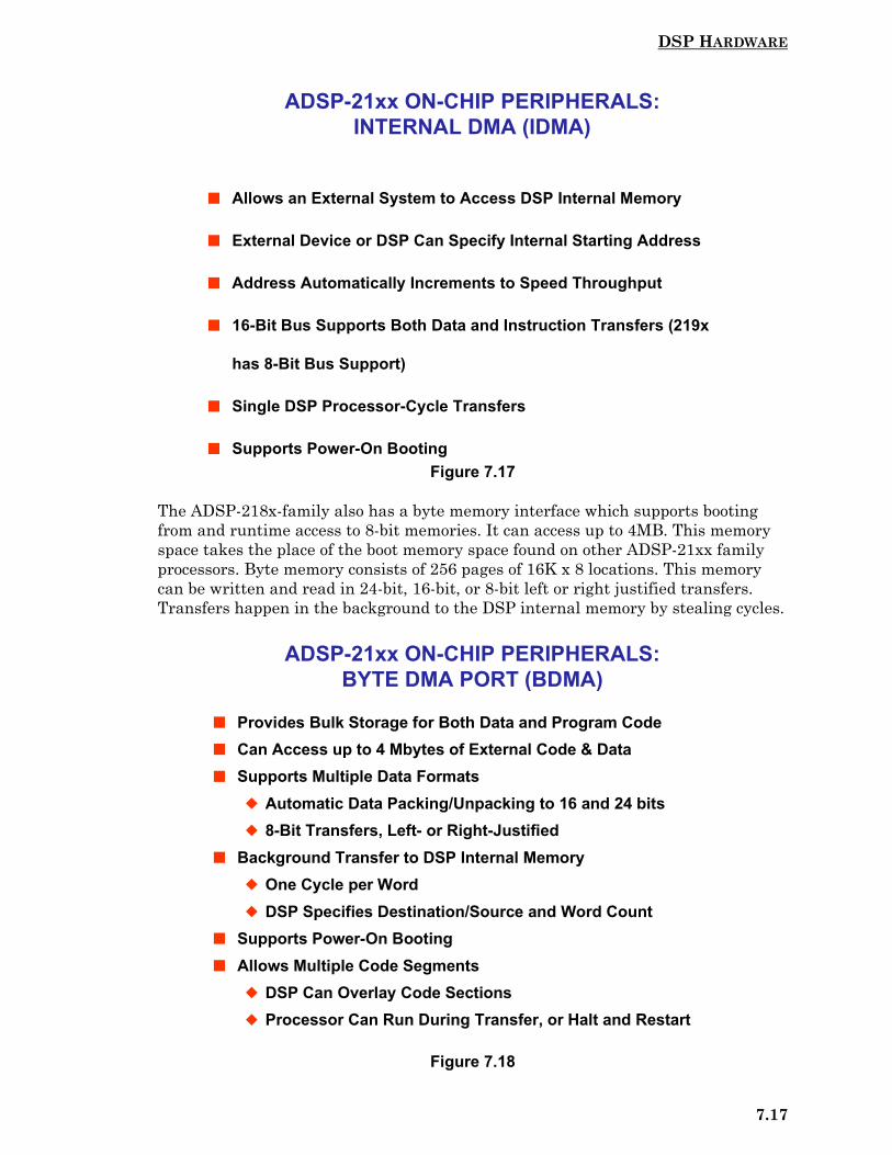
The ADSP-218x-family internal direct-memory-access (IDMA) port supports bootingfrom and runtime access by a host processor. This feature allows data to betransferred to and from internal memory in the background while continuingforeground processing. The IDMA port allows a host processor to access all of theDSPs internal memory without using mailbox registers. The IDMA port supports 16and 24-bit words, and 24-bit transfers take two cycles to complete.
ADSP-21xx ON-CHIP PERIPHERALS:SERIAL PORTS (SPORTs)
� ADSP-21xx SPORTs Are Used For Synchronous Communication
� Full Duplex
� Fully Programmable
� Autobuffer/DMA Capability
� TDM Multi-Channel Capability
� A-law and u-law Companding
� Data Rates of 25 Mbits/sec and Above
� Glueless Interface to a Wide Range of Serial Peripherals or
Processors
� 219x DSPs Add SPI and UART Serial Ports (With Boot Capability)
DSP HARDWARE
7.17
Figure 7.17
The ADSP-218x-family also has a byte memory interface which supports bootingfrom and runtime access to 8-bit memories. It can access up to 4MB. This memoryspace takes the place of the boot memory space found on other ADSP-21xx familyprocessors. Byte memory consists of 256 pages of 16K x 8 locations. This memorycan be written and read in 24-bit, 16-bit, or 8-bit left or right justified transfers.Transfers happen in the background to the DSP internal memory by stealing cycles.
Figure 7.18
ADSP-21xx ON-CHIP PERIPHERALS:INTERNAL DMA (IDMA)
� Allows an External System to Access DSP Internal Memory
� External Device or DSP Can Specify Internal Starting Address
� Address Automatically Increments to Speed Throughput
� 16-Bit Bus Supports Both Data and Instruction Transfers (219x
has 8-Bit Bus Support)
� Single DSP Processor-Cycle Transfers
� Supports Power-On Booting
ADSP-21xx ON-CHIP PERIPHERALS:BYTE DMA PORT (BDMA)
� Provides Bulk Storage for Both Data and Program Code� Can Access up to 4 Mbytes of External Code & Data� Supports Multiple Data Formats
� Automatic Data Packing/Unpacking to 16 and 24 bits� 8-Bit Transfers, Left- or Right-Justified
� Background Transfer to DSP Internal Memory� One Cycle per Word� DSP Specifies Destination/Source and Word Count
� Supports Power-On Booting� Allows Multiple Code Segments
� DSP Can Overlay Code Sections� Processor Can Run During Transfer, or Halt and Restart

DSP HARDWARE
7.18
The ADSP-217x, ADSP-218x, and ADSP-21msp5x devices provide a powerdownfeature that allows the processor to enter a very low power state (less than 1mW)through hardware or software control. This feature is extremely useful for battery-powered applications. During some of the powerdown modes, the internal clocks aredisabled, but the processor registers and memory are maintained.
Figure 7.19
From the above discussions it should be obvious that the ADI DSPs are designed formaximum efficiency when performing typical DSP functions such as FFTs or digitalfiltering. ADI DSPs can perform several operations in an instruction cycle as hasbeen shown in the above filter example. DSPs are often rated in terms of Millions ofInstructions per Second, or MIPS. However, the MIPS rating does not tell the entirestory. For example if processor A has a instruction rate of 50 MIPS and can perform1 operation per instruction, it can perform 50 Million Operations per Second, or 50MOPS. Now assume that processor B has an instruction rate of 20 MIPS, but canperform 4 operations per instruction. Processor B can therefore perform 80 MillionOperations per Second, or 80 MOPS, and is actually more efficient than processor A.A better way to evaluate DSP performance is to use well defined benchmarks suchan FIR filter with a prescribed number of taps or an FFT of known size. Benchmarkcomparisons eliminate the confusion often associated with MIPS or MOPS ratingsalone and are discussed later in this section. Even this form of benchmarking doesnot give a true comparison of performance between two processors. Analysis of thetarget system requirements, processor architecture, memory needs and otherfactors must be considered.
ADSP-21xx INTERNAL PERIPHERALS:POWERDOWN
� Non-Maskable Interrupt� Hardware Pin (PWD), or Software Forced
� Holds Processor in CMOS Standby
� Rapid CLKIN-Cycle Recovery
� Acknowledge Handshake (PWDACK)
� Ideal for Battery-Powered Applications
� 219x is Fully Static
DSP HARDWARE
7.19
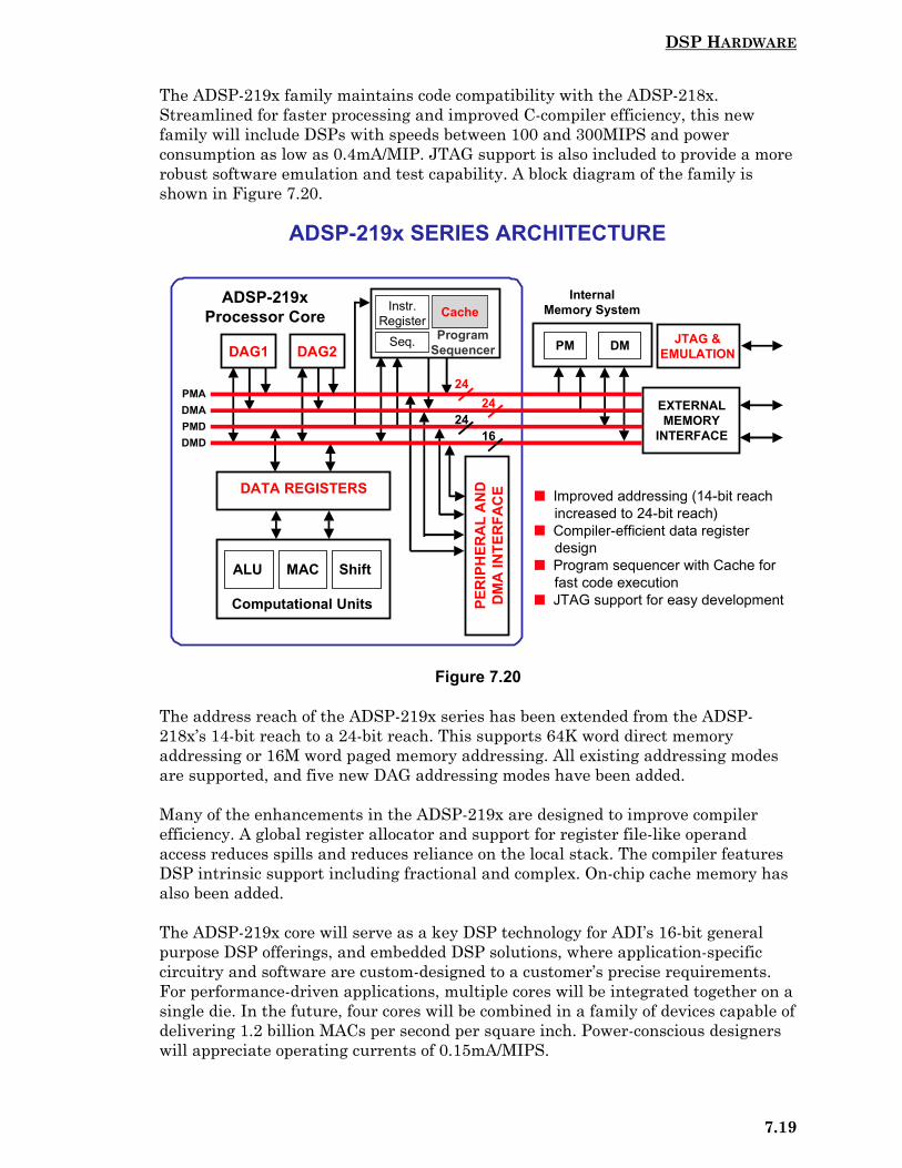
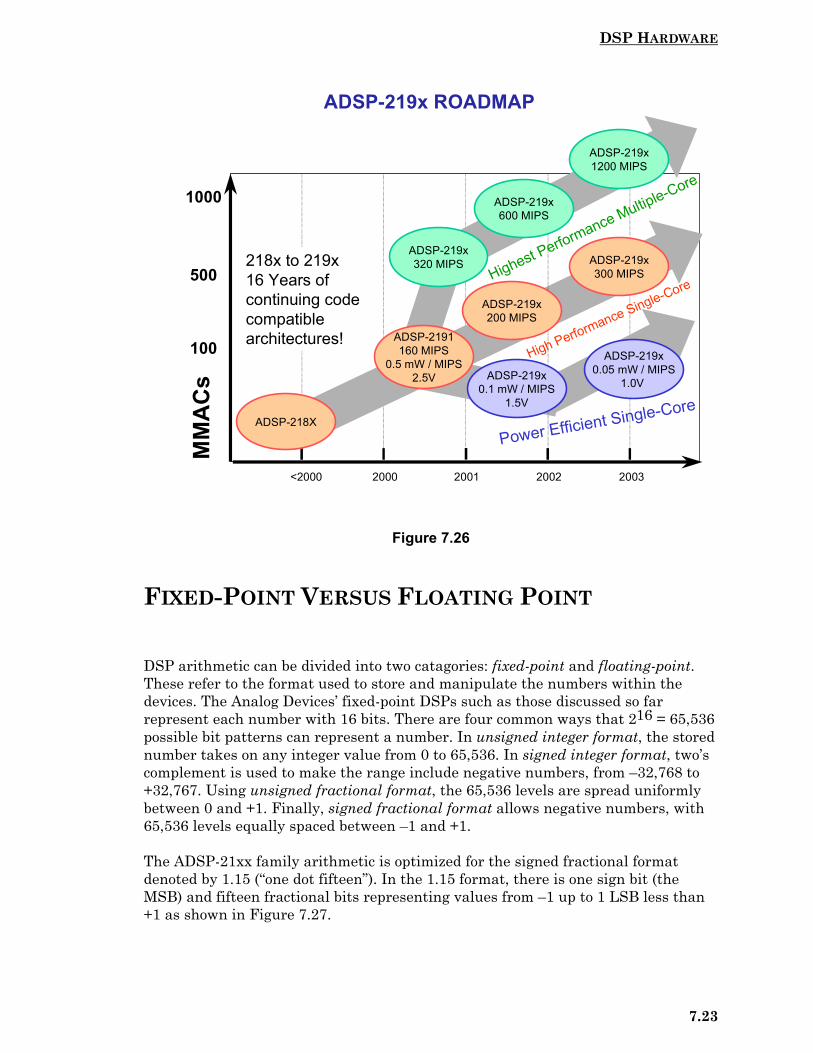
The ADSP-219x family maintains code compatibility with the ADSP-218x.Streamlined for faster processing and improved C-compiler efficiency, this newfamily will include DSPs with speeds between 100 and 300MIPS and powerconsumption as low as 0.4mA/MIP. JTAG support is also included to provide a morerobust software emulation and test capability. A block diagram of the family isshown in Figure 7.20.
Figure 7.20
The address reach of the ADSP-219x series has been extended from the ADSP-218x’s 14-bit reach to a 24-bit reach. This supports 64K word direct memoryaddressing or 16M word paged memory addressing. All existing addressing modesare supported, and five new DAG addressing modes have been added.
Many of the enhancements in the ADSP-219x are designed to improve compilerefficiency. A global register allocator and support for register file-like operandaccess reduces spills and reduces reliance on the local stack. The compiler featuresDSP intrinsic support including fractional and complex. On-chip cache memory hasalso been added.
The ADSP-219x core will serve as a key DSP technology for ADI’s 16-bit generalpurpose DSP offerings, and embedded DSP solutions, where application-specificcircuitry and software are custom-designed to a customer’s precise requirements.For performance-driven applications, multiple cores will be integrated together on asingle die. In the future, four cores will be combined in a family of devices capable ofdelivering 1.2 billion MACs per second per square inch. Power-conscious designerswill appreciate operating currents of 0.15mA/MIPS.
ADSP-219x SERIES ARCHITECTURE
PER
IPH
ERA
L A
ND
DM
A IN
TER
FAC
EDATA REGISTERS
Computational Units
ALU MAC Shift
InternalMemory System
DAG1 DAG2Program
Sequencer PM DM
PMADMAPMDDMD
2424
2416
JTAG &EMULATION
EXTERNALMEMORY
INTERFACE
ADSP-219xProcessor Core CacheInstr.
RegisterSeq.
� Improved addressing (14-bit reach increased to 24-bit reach)� Compiler-efficient data register design� Program sequencer with Cache for fast code execution� JTAG support for easy development

DSP HARDWARE
7.20
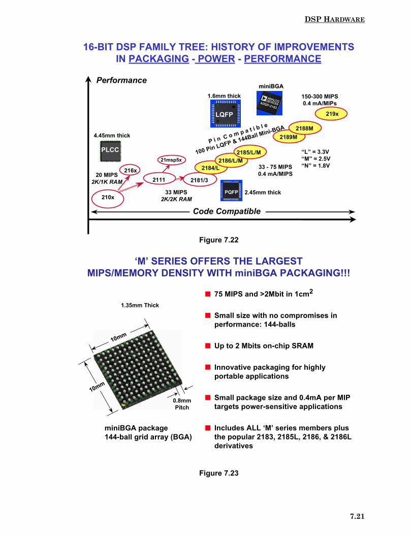
Figure 7.21
The history of the Analog Devices 16-bit fixed-point DSP family is shown in Figure7.22. Notice the migration in performance as well as improvements in powerdissipation and packaging while maintaining code compatibility between thevarious devices. The newer families offer 3.3V (L-series) and 2.5V (M-series)operation for further efficiency. Earlier DSPs were packaged in expensive pin-grid-array (PGA) packages or plastic-leaded-chip-carriers (PLCCs), but these have beenlargely replaced by plastic-quad-flat-packs (PQFPs), and more recently by thin(1.6mm) quad-flat-packs (TQFPs). Note: In 1998, JEDEC changed the specificationsfor the TQFP package designation, assigning it to packages 1.0mm thick. Previouslylabeled TQFP packages (1.6mm thick) are now designated as LQFP per the JEDECspecification.
The 144-ball miniBGA package (see Figure 7.23) from ADI represents innovativepackaging combined with low power consumption (0.4mA per MIP), and allows75MIPS operation and more than 2M bits of SRAM in a 1cm2 package which is1.35mm thick. For example, the 75MIPS ADSP-2188M has 48K of 24-bit programmemory and 56K of 16-bit data memory for a total of 48K×24 + 56K×16 = 2028Kbits with a power dissipation of less than 100mW.
ADSP-219x FAMILY KEY SPECIFICATIONS
� Code Compatible� Compatible with ADSP-218x Series� Single Cycle Instruction Execution, Zero-Over Head Looping,
Single Cycle Context Switch� Performance
� Architectural Performance Beyond 300 MIPs.� Fully Transparent Instruction Cache
� Compiler-Friendly and Tool-Friendly� 64K Word Direct and 16 Mword Paged Memory Support� 5 New DAG Addressing Modes� Register File-Like Operand Access� JTAG Interface Support
DSP HARDWARE
7.21
Figure 7.22
Figure 7.23
‘M’ SERIES OFFERS THE LARGESTMIPS/MEMORY DENSITY WITH miniBGA PACKAGING!!!
miniBGA package144-ball grid array (BGA)
10mm10mm
0.8mmPitch
� 75 MIPS and >2Mbit in 1cm2
� Small size with no compromises inperformance: 144-balls
� Up to 2 Mbits on-chip SRAM
� Innovative packaging for highlyportable applications
� Small package size and 0.4mA per MIPtargets power-sensitive applications
� Includes ALL ‘M’ series members plusthe popular 2183, 2185L, 2186, & 2186Lderivatives
10mm10mm
1.35mm Thick
2181/3
16-BIT DSP FAMILY TREE: HISTORY OF IMPROVEMENTSIN PACKAGING - POWER - PERFORMANCE
2184/L
210x
211120 MIPS
2K/1K RAM
21msp5x
33 MIPS2K/2K RAM
216x
150-300 MIPS0.4 mA/MIPs
2186/L/M 2185/L/M
P i n C o m p a t i b l e
100 Pin LQFP & 144Ball Mini-BGA 2189M
219x
33 - 75 MIPS0.4 mA/MIPS
2188M
miniBGAminiBGA
LQFP
PLCC
PQFP
Code Compatible
Performance
“L” = 3.3V“M” = 2.5V“N” = 1.8V
1.6mm thick
4.45mm thick
2.45mm thick
DSP HARDWARE
7.22
Figure 7.24
Figure 7.25
10 - 33 MIPS32K - 80KBits
ADI 16-Bit DSP ROADMAP16 Years of Code Compatibility & Beyond
500
1000
1985 2000+
MM
AC
s
29-80 MIPS160K - 2MBits
150-300 MIPS640K - 32MBits
312 - 600 MIPS8M - 16MBits
600 - 1200 MIPS16M - 128MBits
Complete Code Compatibility
• As Low as 6mW/MIPS• As High as 0.1MIP/mm2
• As Low as 0.5mW/MIPS• As High as 8MIPs/mm2
• As Low as 0.7mW/MIPS• As High as 0.5MIP/mm2
• As Low as 0.6mW/MIPS• As High as 0.8MIP/mm2
• As Low as 0.4mW/MIPS• As High as 3MIPs/mm2
Single Core Devices
Multiple CoreDevices
100
2100 Core
219x Core
218x Core
29-52 MIPS160K- 1.2MBits
SRAM
500
1994 2000+
MM
AC
s
75 MIPS320K - 2MBits
SRAM
80 MIPS640K -2MBits
SRAM
600 MIPS16MBits SRAM
600 MIPS16MBits SRAM
Code & Pin Compatible Options
• As Low as 2.6mW/MIPS• As High as 0.5MIP/mm2
• 0.7mW/MIPS• 0.5MIPs/mm2
• 1mW/MIPS• 0.5MIP/mm2
•As Low as 1mW/MIPS•As High as 0.75MIP/mm2
•As Low as 0.7mW/MIPS•As High as 0.8MIPs/mm2
Single CoreDevices
MultipleCoreDevices
100
5/3.3V
1.8V
2.5V
1.5V
312 MIPS8MBits SRAM
• 2.6mW/MIPS• 0.3MIP/mm2
40 MIPS640K -2MBits
SRAM
•As Low as 0.6mW/MIPS•As High as 0.4MIPs/mm2
ADSP-218x ROADMAP
DSP HARDWARE
7.23
Figure 7.26
FIXED-POINT VERSUS FLOATING POINT
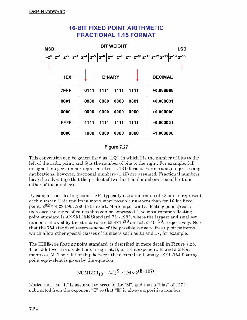
DSP arithmetic can be divided into two catagories: fixed-point and floating-point.These refer to the format used to store and manipulate the numbers within thedevices. The Analog Devices’ fixed-point DSPs such as those discussed so farrepresent each number with 16 bits. There are four common ways that 216 = 65,536possible bit patterns can represent a number. In unsigned integer format, the storednumber takes on any integer value from 0 to 65,536. In signed integer format, two’scomplement is used to make the range include negative numbers, from –32,768 to+32,767. Using unsigned fractional format, the 65,536 levels are spread uniformlybetween 0 and +1. Finally, signed fractional format allows negative numbers, with65,536 levels equally spaced between –1 and +1.
The ADSP-21xx family arithmetic is optimized for the signed fractional formatdenoted by 1.15 (“one dot fifteen”). In the 1.15 format, there is one sign bit (theMSB) and fifteen fractional bits representing values from –1 up to 1 LSB less than+1 as shown in Figure 7.27.
ADSP-219x ROADMAP
<2000 2000 2001 2002 2003
ADSP-219x300 MIPS
ADSP-2191160 MIPS
0.5 mW / MIPS2.5V
ADSP-219x320 MIPS
ADSP-219x600 MIPS
ADSP-219x1200 MIPS
ADSP-219x200 MIPS
ADSP-218X
High Performance Single-Core
100
500
1000
218x to 219x16 Years of continuing codecompatible architectures!
MM
AC
s ADSP-219x0.1 mW / MIPS
1.5V
ADSP-219x0.05 mW / MIPS
1.0V
Power Efficient Single-Core
Highest Performance Multiple-Core
DSP HARDWARE
7.24
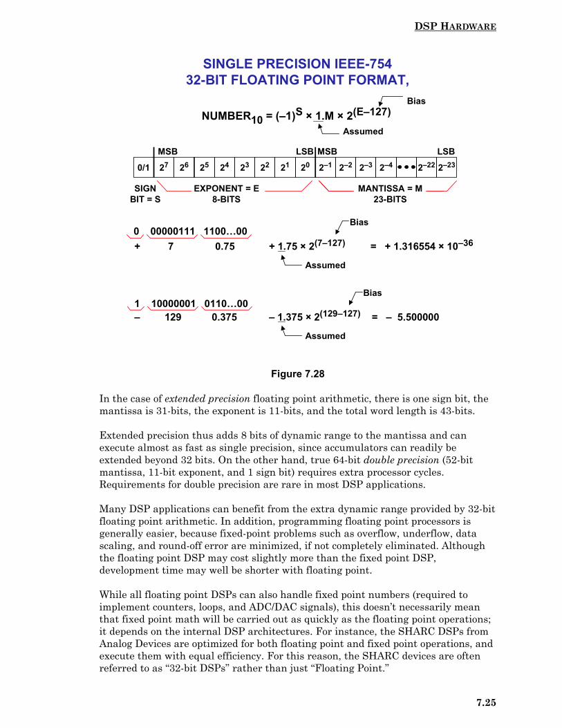
Figure 7.27
This convention can be generalized as “I.Q”, in which I is the number of bits to theleft of the radix point, and Q is the number of bits to the right. For example, fullunsigned integer number representation is 16.0 format. For most signal processingapplications, however, fractional numbers (1.15) are assumed. Fractional numbershave the advantage that the product of two fractional numbers is smaller thaneither of the numbers.
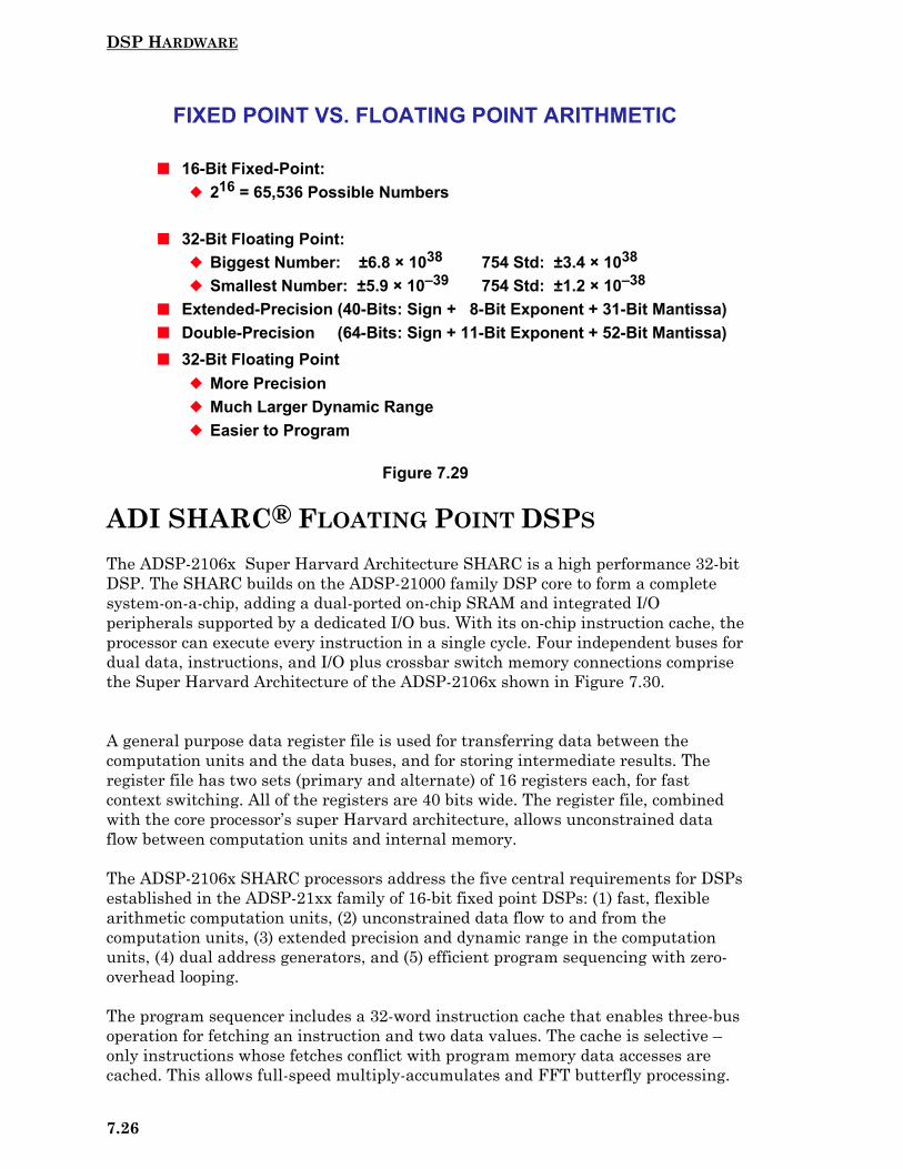
By comparison, floating point DSPs typically use a minimum of 32 bits to representeach number. This results in many more possible numbers than for 16-bit fixedpoint, 232 = 4,294,967,296 to be exact. More importantly, floating point greatlyincreases the range of values that can be expressed. The most common floatingpoint standard is ANSI/IEEE Standard 754-1985, where the largest and smallestnumbers allowed by the standard are ±3.4×1038 and ±1.2×10–38, respectively. Notethat the 754 standard reserves some of the possible range to free up bit patternswhich allow other special classes of numbers such as ±0 and ±∞, for example.
The IEEE-754 floating point standard is described in more detail in Figure 7.28.The 32-bit word is divided into a sign bit, S, an 8-bit exponent, E, and a 23-bitmantissa, M. The relationship between the decimal and binary IEEE-754 floatingpoint equivalent is given by the equation:
)127E(2M.1S)1(10NUMBER −××−= .
Notice that the “1.” is assumed to precede the “M”, and that a “bias” of 127 issubtracted from the exponent “E” so that “E” is always a positive number.
16-BIT FIXED POINT ARITHMETICFRACTIONAL 1.15 FORMAT
–20 2–1 2–2 2–3 2–4 2–5 2–6 2–7 2–8 2–9 2–10 2–11 2–12 2–13 2–14 2–15
HEX BINARY DECIMAL
7FFF
0001
0000
FFFF
8000
0111
0000
0000
1111
1000
1111
0000
0000
1111
0000
1111
0000
0000
1111
0000
1111
0001
0000
1111
0000
+0.999969
+0.000031
+0.000000
–0.000031
–1.000000
BIT WEIGHTMSB LSB
DSP HARDWARE
7.25
Figure 7.28
In the case of extended precision floating point arithmetic, there is one sign bit, themantissa is 31-bits, the exponent is 11-bits, and the total word length is 43-bits.
Extended precision thus adds 8 bits of dynamic range to the mantissa and canexecute almost as fast as single precision, since accumulators can readily beextended beyond 32 bits. On the other hand, true 64-bit double precision (52-bitmantissa, 11-bit exponent, and 1 sign bit) requires extra processor cycles.Requirements for double precision are rare in most DSP applications.
Many DSP applications can benefit from the extra dynamic range provided by 32-bitfloating point arithmetic. In addition, programming floating point processors isgenerally easier, because fixed-point problems such as overflow, underflow, datascaling, and round-off error are minimized, if not completely eliminated. Althoughthe floating point DSP may cost slightly more than the fixed point DSP,development time may well be shorter with floating point.
While all floating point DSPs can also handle fixed point numbers (required toimplement counters, loops, and ADC/DAC signals), this doesn’t necessarily meanthat fixed point math will be carried out as quickly as the floating point operations;it depends on the internal DSP architectures. For instance, the SHARC DSPs fromAnalog Devices are optimized for both floating point and fixed point operations, andexecute them with equal efficiency. For this reason, the SHARC devices are oftenreferred to as “32-bit DSPs” rather than just “Floating Point.”
EXPONENT = E8-BITS
SINGLE PRECISION IEEE-75432-BIT FLOATING POINT FORMAT,
0/1 27 26 25 24 23 22 21 20 2–1 2–2 2–3 2–4 2–22 2–23LSBMSBLSBMSB
MANTISSA = M23-BITS
SIGNBIT = S
0 00000111 1100…00
1 10000001 0110…00
+ 7 0.75 + 1.75 × 2(7–127) = + 1.316554 × 10–36
– 129 0.375 – 1.375 × 2(129–127) = – 5.500000
Bias
Bias
Assumed
Assumed
NUMBER10 = (–1)S × 1.M × 2(E–127)
Assumed
Bias
DSP HARDWARE
7.26
Figure 7.29
ADI SHARC® FLOATING POINT DSPS
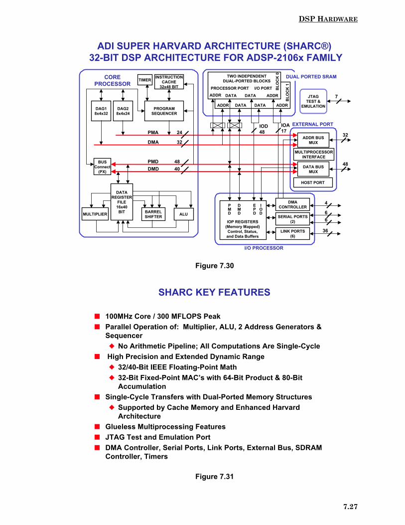
The ADSP-2106x Super Harvard Architecture SHARC is a high performance 32-bitDSP. The SHARC builds on the ADSP-21000 family DSP core to form a completesystem-on-a-chip, adding a dual-ported on-chip SRAM and integrated I/Operipherals supported by a dedicated I/O bus. With its on-chip instruction cache, theprocessor can execute every instruction in a single cycle. Four independent buses fordual data, instructions, and I/O plus crossbar switch memory connections comprisethe Super Harvard Architecture of the ADSP-2106x shown in Figure 7.30.
A general purpose data register file is used for transferring data between thecomputation units and the data buses, and for storing intermediate results. Theregister file has two sets (primary and alternate) of 16 registers each, for fastcontext switching. All of the registers are 40 bits wide. The register file, combinedwith the core processor’s super Harvard architecture, allows unconstrained dataflow between computation units and internal memory.
The ADSP-2106x SHARC processors address the five central requirements for DSPsestablished in the ADSP-21xx family of 16-bit fixed point DSPs: (1) fast, flexiblearithmetic computation units, (2) unconstrained data flow to and from thecomputation units, (3) extended precision and dynamic range in the computationunits, (4) dual address generators, and (5) efficient program sequencing with zero-overhead looping.
The program sequencer includes a 32-word instruction cache that enables three-busoperation for fetching an instruction and two data values. The cache is selective –only instructions whose fetches conflict with program memory data accesses arecached. This allows full-speed multiply-accumulates and FFT butterfly processing.
FIXED POINT VS. FLOATING POINT ARITHMETIC
� 16-Bit Fixed-Point:� 216 = 65,536 Possible Numbers
� 32-Bit Floating Point:� Biggest Number: ±6.8 × 1038 754 Std: ±3.4 × 1038
� Smallest Number: ±5.9 × 10–39 754 Std: ±1.2 × 10–38
� Extended-Precision (40-Bits: Sign + 8-Bit Exponent + 31-Bit Mantissa)� Double-Precision (64-Bits: Sign + 11-Bit Exponent + 52-Bit Mantissa)� 32-Bit Floating Point
� More Precision� Much Larger Dynamic Range� Easier to Program
DSP HARDWARE
7.27
Figure 7.30
Figure 7.31
SHARC KEY FEATURES
� 100MHz Core / 300 MFLOPS Peak� Parallel Operation of: Multiplier, ALU, 2 Address Generators &
Sequencer� No Arithmetic Pipeline; All Computations Are Single-Cycle
� High Precision and Extended Dynamic Range� 32/40-Bit IEEE Floating-Point Math� 32-Bit Fixed-Point MAC’s with 64-Bit Product & 80-Bit
Accumulation� Single-Cycle Transfers with Dual-Ported Memory Structures
� Supported by Cache Memory and Enhanced HarvardArchitecture
� Glueless Multiprocessing Features� JTAG Test and Emulation Port� DMA Controller, Serial Ports, Link Ports, External Bus, SDRAM
Controller, Timers
ADI SUPER HARVARD ARCHITECTURE (SHARC®) 32-BIT DSP ARCHITECTURE FOR ADSP-2106x FAMILY
TIMER INSTRUCTIONCACHE
32x48 BIT
PROGRAMSEQUENCER
DAG18x4x32
BUSConnect
(PX)
DATAREGISTER
FILE16x40BITMULTIPLIER BARREL
SHIFTER ALU
DAG28x4x24
DMACONTROLLER
SERIAL PORTS(2)
LINK PORTS(6)
IOP REGISTERS(Memory Mapped)Control, Status,and Data Buffers
PMD
DMD
EPD
IOD
ADDR BUSMUX
MULTIPROCESSORINTERFACE
DATA BUSMUX
HOST PORT
JTAGTEST &
EMULATION
TWO INDEPENDENTDUAL-PORTED BLOCKS
PROCESSOR PORT I/O PORTADDR DATA DATA ADDR
DATAADDR DATA ADDR
COREPROCESSOR
BLO
CK
0
BLO
CK
1
DUAL PORTED SRAM
EXTERNAL PORT
I/O PROCESSOR
PMA
DMA
PMDDMD
24
32
4840
7
32
48
4
66
36
IOD48
IOA17

DSP HARDWARE
7.28
Figure 7.32
The ADSP-2106x family execute all instructions in a single cycle. They handle 32-bitIEEE floating point format, 32-bit integer and fractional fixed point formats (twos-complement and unsigned), and extended precision 40-bit IEEE floating pointformat. The processors carry extended precision throughout their computationunits, minimizing intermediate data truncation errors. When working with data on-chip, the extended precision 32-bit mantissa can be transferred to and from allcomputation units. The 40-bit data bus may be extended off-chip if desired. Thefixed point formats have an 80-bit accumulator for true 32-bit fixed pointcomputations.
The ADSP-2106x has a super Harvard architecture combined with a 10-port dataregister file. In every cycle, (1) two operands can be read or written to or from theregister file, (2) two operands can be supplied to the ALU, (3) two operands can besupplied to the multiplier, and (4) two results can be received from the ALU andmultiplier.
The ADSP-2106x family instruction set provides a wide variety of programmingcapabilities. Multifunction instructions enable computations in parallel with datatransfers, as well as simultaneous multiplier and ALU operations.
SHARC® THE LEADER IN FLOATING POINT DSP
� SHARC is the de facto standard in multiprocessing� ADSP-21160 continues SHARC leadership in multiprocessing� ADSP-21065L is the right choice for low-cost floating point
SUPER HARVARD ARCHITECTURE:Balancing Memory, I/O and Computational
Power...� High Performance Computation Unit� Four Bus Performance
� Fetch Next Instruction� Access 2 data values� Perform DMA for I/O
� Memory Architecture� Non Intrusive DMA

DSP HARDWARE
7.29
The ADSP-21060 contains 4 Mbits of on-chip SRAM, organized as two blocks of 2Mbits each, which can be configured for different combinations of code and datastorage. The ADSP-21062, ADSP-21061 and ADSP-21065 each include 2 Mbit,1Mbit and 544Kbits of on-chip SRAM, respectively. Each memory block is dual-ported for single-cycle, independent accesses by the core processor and I/O processoror DMA controller. The dual-ported memory and separate on-chip buses allow twodata transfers from the core and one from I/O, all in a single cycle.
While each memory block can store combinations of code and data, accesses aremost efficient when one block stores instructions and data, using the DM bus fortransfers, and the other block stores instructions and data, using the PM bus fortransfers. Using the DM bus and PM bus in this way, with one dedicated to eachmemory block, assures single-cycle execution with two data transfers. In this case,the instruction must be available in the cache. Single-cycle execution is alsomaintained when one of the data operands is transferred to or from off-chip, via theADSP-2106x’s external port.
The ADSP-2106x’s external port provides the processor’s interface to off-chipmemory and peripherals. The 4 Gword off-chip address space is included in theADSP-2106x’s unified address space. The separate on-chip buses – for PMaddresses, PM data, and DM addresses, DM data, I/O addresses, and I/O data – aremultiplexed at the external port to create an external system bus with a single 32-bit address bus and a single 48-bit data bus. The ADSP-2106x providesprogrammable memory wait states and external memory acknowledge controls toallow interfacing to DRAM and peripherals with variable access, hold, and disabletime requirements.
The ADSP-2106x’s host interface allows easy connection to standard microprocessorbuses, both 16-bit and 32-bit, with little additional hardware required. Fourchannels of DMA are available for the host interface; code and data transfers areaccomplished with low software overhead. The host can directly read and write theinternal memory of the ADSP-2106x, and can access the DMA channel setup andmailbox registers. Vector interrupt support is provided for efficient execution of hostcommands.
The ADS-2106x offers powerful features tailored to multiprocessing DSP systems.The unified address space allows direct interprocessor accesses of each ADSP-2106x’s internal memory. Distributed bus arbitration logic is included on-chip forsimple, glueless connection of systems containing up to six ADSP-2106xs and a hostprocessor. Master processor changeover incurs only one cycle of overhead. Busarbitration is selectable as either fixed or rotating priority. Maximum throughputfor interprocessor data transfer is 240 Mbytes/second (with a 40MHz clock) over thelink ports or external port.
The ADSP-2106x’s I/O Processor (IOP) includes two serial ports, six 4-bit link ports,and a DMA controller. The ADSP-2106x features two synchronous serial ports thatprovide an inexpensive interface to a wide variety of digital and mixed-signalperipheral devices. The serial ports can operate at the full external clock rate of theprocessor, providing each with a maximum data rate of 50 Mbit/second.Independent transmit and receive functions provide greater flexibility for serialcommunications. Serial port data can be automatically transferred to and from on-

DSP HARDWARE
7.30
chip memory via DMA. Each of the serial ports offers a TDM multichannel mode.They offer optional µ-law or A-law companding. Serial port clocks and frame syncscan be internally or externally generated.
The ADSP-21060 and ADSP-21062 feature six 4-bit link ports that provideadditional I/O capabilities. The link ports can be clocked twice per cycle, allowingeach to transfer 8 bits per cycle. Link port I/O is especially useful for point-to-pointinterprocessor communication in multiprocessing systems. The link ports canoperate independently and simultaneously, with a maximum data throughput of240 Mbytes/second. Link port data is packed into 32-bit or 48-bit words, and can bedirectly read by the core processor or DMA-transferred to on-chip memory. Eachlink port has its own double-buffered input and output registers. Clock/acknowledgehandshaking controls link port transfers. Transfers are programmable as eithertransmit or receive. There are no link ports on the ADSP-21061 or ADSP-21065devices.
The ADSP-2106x’s on-chip DMA controller allows zero-overhead data transferswithout processor intervention. The DMA controller operates independently andinvisibly to the processor core, allowing DMA operations to occur while the core issimultaneously executing its program. Both code and data can be downloaded to theADSP-2106x using DMA transfers. DMA transfers can occur between the ADSP-2106x’s internal memory and external memory, external peripherals, or a hostprocessor. DMA transfers can also occur between the ADSP-2106x’s internalmemory and its serial ports or link ports. DMA transfers between external memoryand external peripheral devices are another option.
The internal memory of the ADSP-2106x can be booted at system powerup from an8-bit EPROM or a host processor. Additionally, the ADSP-21060 and the ADSP-21062 can also be booted through one of the link ports. Both 32-bit and 16-bit hostprocessors can be used for booting.
The ADSP-2106x supports the IEEE standard P1149.1 Joint Test Action Group(JTAG) standard for system test. This standard defines a method for seriallyscanning the I/O status of each component in a system. In-circuit emulators also usethe JTAG serial port to access the processor’s on-chip emulation features. EZ-ICEEmulators use the JTAG test access port to monitor and control the target boardprocessor during emulation. The EZ-ICE in-circuit emulator provides full-speedemulation to enable inspection and modification of memory, registers, and processorstacks. Use of the processor’s JTAG interface assures non-intrusive in-circuitemulation – the emulator does not affect target system loading or timing.
The SHARC architecture avoids processor bottlenecks by balancing core, memory,I/O processor, and peripherals as shown in Figure 7.30. The core supports 32-bitfixed and floating point data. The memory contributes to the balance by offeringlarge size and dual ports. The core can access data from one port, and the other portis used to move data to and from the I/O processor. The I/O processor moves data toand from the peripherals to the internal memory using zero overhead DMAs. Theseoperations run simultaneously to the core operation.

DSP HARDWARE
7.31
ADSP-2116X SINGLE-INSTRUCTION, MULTIPLE-DATA (SIMD) CORE ARCHITECTURE
The ADSP-21160 is the first member of the second-generation ADI 32-bit DSPs. Itscore architecture is shown in Figure 7.33. Notice that the core is similar to theADSP-2106x core except for the width of the buses and the addition of a secondcomputational unit complete with its own multiplier, ALU, shifter, and register file.This architecture is called single-instruction, multiple-data (SIMD) as opposed tosingle-instruction, single-data (SISD). The second computational unit allows theDSP to process multiple data streams in parallel. The core operates at up to 100MIPS. At 100MHz clock operation the core is capable of 400 MFLOPS (millions offloating point operations per second) sustained and 600 MFLOPS peak operation.SIMD is a natural next step in increasing performance for ADI DSPs. Because theirbasic architecture already allows single instruction and multiple data access, addinganother computational unit lets the architecture process the multiple data. TheSIMD architectural extension allows code-compatible higher performance parts.
Figure 7.33
ADSP-2116x CORE PROCESSOR FEATURINGSINGLE-INSTRUCTION, MULTIPLE-DATA (SIMD)
TIMER INSTRUCTIONCACHE
32x48 BIT
PROGRAMSEQUENCER
DAG18x4x32
BUSConnect
(PX)
DATAREGISTER
FILE(PEx)16x40
BITMULTIPLIER BARRELSHIFTER ALU
DAG28x4x32
PMA
DMA
PMD
DMD
32
32
16/32/40/48/64
32/40/64
DATAREGISTER
FILE(PEy)16x40
BITMULTIPLIER BARRELSHIFTER ALU
ADSP-2116xCORE PROCESSOR

DSP HARDWARE
7.32
The SIMD features of the ADSP-2116x include two computational units (PEx, PEy)and double data-word size buses (DMD and PMD). The primary processing element,PEx, is always enabled. The secondary processing element, PEy, is mode controlenabled. The double wide data buses provide each computational unit with its owndata set in each cycle. With SIMD enabled, both processing elements execute thesame instruction each cycle (that’s the Single-Instruction), but they execute thatinstruction using different data (that’s the Multiple-Data). The SIMD-basedperformance increase appears in algorithms that can be optimized by splitting theprocessing of data between the two computational units. By taking advantage of thesecond computational unit the cycle time can be cut in half compared to the SISDapproach for many algorithms.
The ADSP-21160 has a complete set of integrated peripherals: I/O Processor, 4Mbyte on-chip dual-ported SRAM, glueless multiprocessing features, and ports(serial, link, external bus, host, and JTAG). Power dissipation is approximately 2Wat 100MHz in a 400-ball 27 × 27mm PBGA package. The complete SHARC familyroadmap is shown in Figure 7.35.
Figure 7.34
Figure 7.36 shows some typical coding using the SHARC family of DSPs. Note thealgebraic syntax of the assembly language which facilitates coding of algorithmsand reading the code after it is written. In a single cycle, the SHARC performsmultiplication, addition, subtraction, memory read, memory write, and addresspointer updates. In the same cycle, the I/O processor can transfer data to and fromthe serial port, the link ports, memory or DMA, and update the DMA pointer.
ADSP-21160 32-BIT SHARC KEY FEATURES
� SIMD (Single-Instruction, Multiple-Data) Architecture
� Code Compatible with ADSP-2106x Family
� 100 MHz Core / 600 MFLOPS Peak
� On-Chip Peripherals Similar to ADSP-2106x Family
� Dual-Ported 4Mbit SRAM
� Glueless Multiprocessing Features
� 400-Ball, PBGA 27×27mm Package

DSP HARDWARE
7.33
Figure 7.35
Figure 7.36
SHARC ROADMAPCommitment to Code Compatibility Into Tomorrow
• 120-198 MFLOPS• 0.5 - 4 Mbits Memory
MP HP SHARC
Low CostHP SHARC
ADSP-21161N• 1200 MFLOPs• <<$10 SHARC
• 10 GFLOPs• 64 Mbits
MULTIPROCESSING
MASS MARKET
ADSP-21060
ADSP-21062
ADSP-21065ADSP-21061
ADSP-21160M
EXAMPLE: SHARC MULTI-FUNCTION INSTRUCTION
f11 = f1 * f7, f3 = f9 + f14, f9 = f9 – f14, dm (i2, m0) = f13, f7 = pm (i8, m8);� In this Single-Cycle Instruction the SHARC Performs:
� 1 (2) Multiply� 1 (2) Addition� 1 (2) Subtraction� 1 (2) Memory Read� 1 (2) Memory Write� 2 Address Pointer Updates
� Plus the I/O Processor Performs:� Active Serial Port Channels: Transmit and Receive on all Ports� 6 Active Link Ports if Present� Memory DMA� 2 (4) DMA Pointer Updates
The Algebraic Syntax of the Assembly Language Facilitates Coding ofDSP Algorithms
( ) = ADSP-2116x SIMD DSP

DSP HARDWARE
7.34
MULTIPROCESSING USING SHARCS
Analog Devices’ SHARC DSPs such as the ADSP-21160 are optimized formultiprocessing applications such as telephony, medical imaging, radar/sonar,communications, 3D graphics and imaging. Figure 7.37 shows SHARC benchmarkperformance on common DSP algorithms.
Figure 7.37
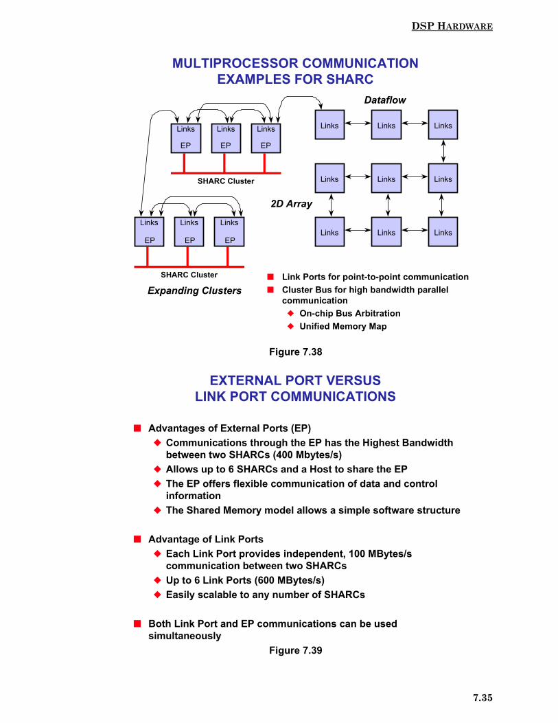
Multiprocessor systems typically use one or both of two methods to communicatebetween processor nodes. One method uses dedicated point-to-point communicationchannels. This method is often called data-flow multiprocessing. In the othermethod, nodes communicate through a single shared global memory via a parallelbus. The SHARC family supports the implementation of point-to-pointcommunication through its six link ports called link port multiprocessing. It alsosupports an enhanced version of shared parallel bus communication called clustermultiprocessing.
For applications that require high computational bandwidth, but only limitedflexibility, data flow multiprocessing is the best solution. The DSP algorithm ispartitioned sequentially across several processors and data is passed directly acrossthem as shown on the right side of Figure 7.38. The SHARC is ideally suited fordata flow multiprocessing applications because it elminates the need forinterprocessor data FIFOs and external memory. Each SHARC has six link portsallowing 2D and 3D arrays as well as traditional data flow. The internal memory ofthe SHARC is usually large enough to contain both code and data for mostapplications using this topology. All a data flow system requires are a number ofSHARC processors and point-to-point signals connecting them.
DSP BENCHMARKS FOR SHARC FAMILY
ADSP-21065LSHARC
ADSP-21160SISD
ADSP-21160 SIMD/multiple channels
Clock Cycle 66 MHz 100 MHz 100 MHzInstruction Cycle Time 15 ns 10 ns 10 nsMFLOPS Sustained 132 MFLOPS 200 MFLOPS 400 MFLOPSMFLOPS Peak 198 MFLOPS 300 MFLOPS 600 MFLOPS1024 Point Complex FFT(Radix 4, with reversal)
274 µs 180 µs 90 µs
FIR Filter (per tap) 15 ns 10 ns 5 nsIIR Filter (per biquad) 60 ns 40 ns 20 nsMatrix Multiply(pipelined)[3x3] * [3x1][4x4] * [4x1]
135 ns240 ns
90 ns160 ns
45 ns80 ns
Divide (y/x) 90 ns 60 ns 30 nsSquare Root 135 ns 90 ns 45 ns
DSP HARDWARE
7.35
Figure 7.38
Figure 7.39
MULTIPROCESSOR COMMUNICATIONEXAMPLES FOR SHARC
EP EP EP
Links Links Links
SHARC Cluster
EP EP EP
Links Links Links
SHARC Cluster Links Links
Links Links
Links Links Links
Links
Links
2D Array
Dataflow
Expanding Clusters� Link Ports for point-to-point communication� Cluster Bus for high bandwidth parallel
communication� On-chip Bus Arbitration� Unified Memory Map
EXTERNAL PORT VERSUSLINK PORT COMMUNICATIONS
� Advantages of External Ports (EP)� Communications through the EP has the Highest Bandwidth
between two SHARCs (400 Mbytes/s)� Allows up to 6 SHARCs and a Host to share the EP� The EP offers flexible communication of data and control
information� The Shared Memory model allows a simple software structure
� Advantage of Link Ports� Each Link Port provides independent, 100 MBytes/s
communication between two SHARCs� Up to 6 Link Ports (600 MBytes/s)� Easily scalable to any number of SHARCs
� Both Link Port and EP communications can be usedsimultaneously
DSP HARDWARE
7.36
Cluster multiprocessing is best suited for applications where a fair amount offlexibility is required. This is especially true when a system must be able to supporta variety of different tasks, some of which may be running concurrently. SHARCprocessors also have an on-chip host interface that allows a cluster to be easilyinterfaced to a host processor or even to another cluster.
Cluster multiprocessing systems include multiple SHARC processors connected by aparallel bus that allows interprocessor access of on-chip memory as well as access toshared global memory. In a typical cluster of SHARCs, up to six ADSP-21160processors and a host can arbitrate for the bus. The on-chip bus arbitration logicallows these processors to share the common bus. The SHARC’s other on-chipfeatures help eliminate the need for any extra glue hardware in the clustermultiprocessor configuration. External memory, both local and global, canfrequently be eliminated in this type of system.
TIGERSHARC™: THE ADSP-TS001 STATICSUPERSCALAR DSPThe ADSP-TS001 is the first DSP from Analog Devices to use the newTigerSHARC™ static superscalar architecture. The TigerSHARC targetstelecommunications infrastructure equipment with a new level of integration andthe unique ability to process 8-, 16-, 32-bit fixed and floating-point data types on asingle chip. Each of these data types is critical to the next generation oftelecommunications protocols currently under development, including IMT-2000(also known as 3G wireless) and xDSL (digital subscriber line). Unlike any otherDSP, the ADSP-TS001 has the unique ability to accelerate processing speed basedon the data type. Moreover, the chip delivers the highest performance floating-pointprocessing.
In telecommunications infrastructure equipment, voice coder and channel coderprotocols are developed around 16-bit data types. To improve signal quality, manytelecom applications employ line equalization and echo cancellation techniques thatboost overall signal quality and system performance. These algorithms benefit fromthe added precision of 32-bit and floating-point data processing. The 8-bit nativesupport is well suited to the commonly used Viterbi channel decoder algorithm, aswell as image processing where it is more straightforward and cost-effective torepresent red, green, and blue components of the signal with 8-bit data types. Manyof these applications require high levels of performance and may require algorithmsto be executed consecutively or even concurrently. The end application determinesthe exact requirements. The flexibility of the TigerSHARC architecture enables thesoftware engineer to match the application precision requirements without any lossof system performance. In the TigerSHARC, performance is traded directly againstnumerical precision.
The TigerSHARC architecture uses key elements from multiple microprocessortypes – RISC (reduced instruction set computer), VLIW (very long instruction word),and DSP in order to provide the highest performance digital signal processingengine. The new architecture leverages existing DSP product attributes such as fastand deterministic execution cycles, highly responsive interrupts, and an excellentperipheral interface to support large core computation rates and a high data rate

DSP HARDWARE
7.37
I/O. To achieve excellent core performance, RISC-like features such as load/storeoperations, a deeply pipelined sequencer with branch prediction, and largeinterlocked register files are introduced. Additionally, the VLIW (very longinstruction word) attributes offer more efficient use of code space, especially forcontrol code.
Figure 7.40
Figure 7.41
DSP
VLIWRISC
TigerSHARC®: ANALOG DEVICES’ NEWSTATIC SUPERSCALER DSP ARCHITECTURE
• Instruction level parallelismdetermined prior to run time inmulti-instruction lines
• Load / store architecture• Deeply pipelined for highclock rates• Branch prediction• Large interlocked registerfile
• Determinism and real-time execution• Fast and responsive interrupt system• I/O and internal memory capable ofsustaining core rates• Fast multiply accumulates, HW support forcircular buffers, bit reverse, zero overheadlooping
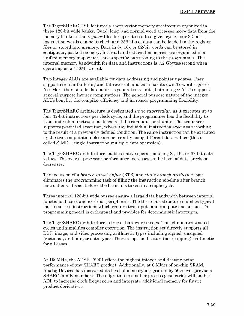
TigerSHARC KEY ARCHITECTURAL FEATURES
Core� 1200 MMACs/s @ 150 MHz -- 16-Bit Fixed Point� 300 MMACs/s @150 MHz -- 32-Bit Floating Point� 900 MFLOPS -- 32-Bit Floating Point
Memory� 6 Mbits of on-chip SRAM organized in a unified memory map as
opposed to the traditional Harvard architecture.
I/O, Peripherals, & Package� 600 Mbytes/s transfer rate through external bus.� 600 Mbytes/s aggregate transfer rate through 4 Link Ports� Glueless multiprocessor cluster support for up to 8 ADSP-TS001s� 4 General Purpose I/O Ports� SDRAM Controller� 360 Ball, SBGA Package 35×35mm
DSP HARDWARE
7.38
Finally, to supply all functional blocks with instructions, clever management of theinstruction word is necessary. Specifically, multiple instructions must be dispatchedto processing units simultaneously, and functional parallelism must be calculatedprior to runtime.
By incorporating the best of all worlds, the TigerSHARC architecture will provide astate of the art platform for the most demanding signal processing applications.
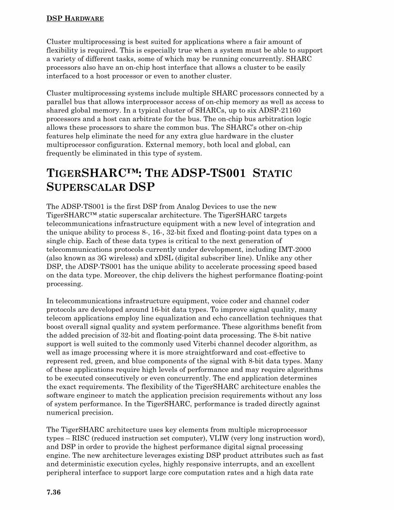
The TigerSHARC core shown in Figure 7.42 consists of multiple functional blocks:computation blocks, memory, integer ALUs, and a sequencer. There are twocomputational blocks (X and Y) in the TigerSHARC architecture, each containing amultiplier, ALU, and 64-bit shifter. With the resources in these blocks, it is possibleto execute eight 40-bit MACs on 16-bit data, two 40-bit MACs on 16-bit complexdata, or two 80-bit MACs on 32-bit data – all in a single cycle. TigerSHARC is aregister-based load/store architecture, where each computational block has access toa fully orthogonal 32-word register file.
Figure 7.42
ADSP-TS001 TigerSHARC® ARCHITECTURE
M02Mbit
128
J ALU
J-RF0
31
128-entryBTB
128128
Comp Block X
EXTERNALPORT
DMA
PERIPHERALS
SEQUENCER K ALU
K-RF0
31
ALU
Mult
Shift
RF
0
31
128 128
128 128 128
128128128
128128
Comp Block Y
ALU
Mult
Shift
RF
0
31
M12Mbit
M22Mbit
MD0MD1
MD2
ON-CHIP SRAM
DSP HARDWARE
7.39
The TigerSHARC DSP features a short-vector memory architecture organized inthree 128-bit wide banks. Quad, long, and normal word accesses move data from thememory banks to the register files for operations. In a given cycle, four 32-bitinstruction words can be fetched, and 256 bits of data can be loaded to the registerfiles or stored into memory. Data in 8-, 16-, or 32-bit words can be stored incontiguous, packed memory. Internal and external memories are organized in aunified memory map which leaves specific partitioning to the programmer. Theinternal memory bandwidth for data and instructions is 7.2 Gbytes/second whenoperating on a 150MHz clock.
Two integer ALUs are available for data addressing and pointer updates. Theysupport circular buffering and bit reversal, and each has its own 32-word registerfile. More than simple data address generations units, both integer ALUs supportgeneral purpose integer computations. The general purpose nature of the integerALUs benefits the compiler efficiency and increases programming flexibility.
The TigerSHARC architecture is designated static superscalar, as it executes up tofour 32-bit instructions per clock cycle, and the programmer has the flexibility toissue individual instructions to each of the computational units. The sequencersupports predicted execution, where any individual instruction executes accordingto the result of a previously defined condition. The same instruction can be executedby the two computation blocks concurrently using different data values (this iscalled SIMD – single-instruction multiple-data operation).
The TigerSHARC architecture enables native operation using 8-, 16-, or 32-bit datavalues. The overall processor performance increases as the level of data precisiondecreases.
The inclusion of a branch target buffer (BTB) and static branch prediction logiceliminates the programming task of filling the instruction pipeline after branchinstructions. If seen before, the branch is taken in a single cycle.
Three internal 128-bit wide busses ensure a large data bandwidth between internalfunctional blocks and external peripherals. The three-bus structure matches typicalmathematical instructions which require two inputs and compute one output. Theprogramming model is orthogonal and provides for deterministic interrupts.
The TigerSHARC architecture is free of hardware modes. This eliminates wastedcycles and simplifies compiler operation. The instruction set directly supports allDSP, image, and video processing arithmetic types including signed, unsigned,fractional, and integer data types. There is optional saturation (clipping) arithmeticfor all cases.
At 150MHz, the ADSP-TS001 offers the highest integer and floating pointperformance of any SHARC product. Additionally, at 6 Mbits of on-chip SRAM,Analog Devices has increased its level of memory integration by 50% over previousSHARC family members. The migration to smaller process geometries will enableADI to increase clock frequencies and integrate additional memory for futureproduct derivatives.
DSP HARDWARE
7.40
Figure 7.43
The ADSP-TS001 reduces total material costs by integrating multiple I/O andperipheral functions that reduce or eliminate the need for external glue logic andsupport chips. Specifically, the ADSP-TS001 at 150MHz integrates four gluelesslink ports with an aggregate transfer rate of 600 Mbytes/s, glueless multiprocessorcluster interface support for up to 8 ADSP-TS001s, an SDRAM controller, and aJTAG controller. This unprecedented functionality is packaged in a 35 by 35mm 360ball SBGA package.
Typical computation rates and coding details of the TigerSHARC are shown inFigure 7.44. Four 32-bit instructions are executed in parallel forming one 128-bitinstruction line. The entire instruction line is executed in one cycle. This exampleassembly code is for a single line and is performing the following:
xR3:0=Q[j0+=4];// load 4 registers (xR0,xR1,xR2,xR3) in the X register file frommemory
yR3:0=Q[k0+=4];// load 4 registers in the Y register file from memory
FR5=R4*R4; // multiply 2 32-bit floats in X computational block and2 more in Y (2 multiplies)
FR9:8=R6+/-R7;;// add and subtract in both X and Y computational blocks(4 ALU operations)
TigerSHARC KEY FEATURES
Execution of 1 to 4 32-Bit Instructions Per Clock Cycle
Single-Instruction Multiple Data (SIMD) OperationsSupported by Two Computation Blocks
Multiple Data Type Computation Blocks� Each With Register File, MAC, ALU, Shifter� 32/40-Bit Floating or 32-Bit Fixed Point Operations (6
Per Cycle)� 16-Bit (24 Per Cycle) or 8-Bit (32 Per Cycle)
Operations
Static Branch Prediction Mechanism, with 128-EntryBranch Target Buffer (BTB)
Internal Bandwidth of 7.2 Gbytes/second
Simple and Fully Interruptible Programming Model
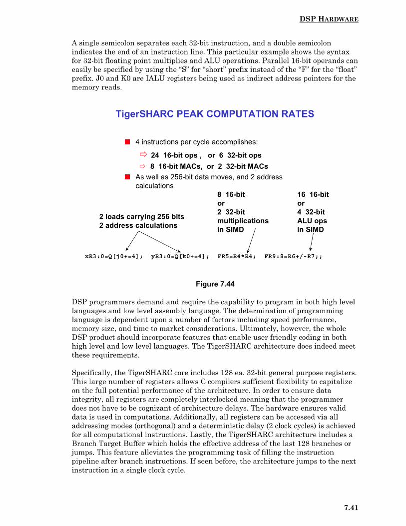
DSP HARDWARE
7.41
A single semicolon separates each 32-bit instruction, and a double semicolonindicates the end of an instruction line. This particular example shows the syntaxfor 32-bit floating point multiplies and ALU operations. Parallel 16-bit operands caneasily be specified by using the “S” for “short” prefix instead of the “F” for the “float”prefix. J0 and K0 are IALU registers being used as indirect address pointers for thememory reads.
Figure 7.44
DSP programmers demand and require the capability to program in both high levellanguages and low level assembly language. The determination of programminglanguage is dependent upon a number of factors including speed performance,memory size, and time to market considerations. Ultimately, however, the wholeDSP product should incorporate features that enable user friendly coding in bothhigh level and low level languages. The TigerSHARC architecture does indeed meetthese requirements.
Specifically, the TigerSHARC core includes 128 ea. 32-bit general purpose registers.This large number of registers allows C compilers sufficient flexibility to capitalizeon the full potential performance of the architecture. In order to ensure dataintegrity, all registers are completely interlocked meaning that the programmerdoes not have to be cognizant of architecture delays. The hardware ensures validdata is used in computations. Additionally, all registers can be accessed via alladdressing modes (orthogonal) and a deterministic delay (2 clock cycles) is achievedfor all computational instructions. Lastly, the TigerSHARC architecture includes aBranch Target Buffer which holds the effective address of the last 128 branches orjumps. This feature alleviates the programming task of filling the instructionpipeline after branch instructions. If seen before, the architecture jumps to the nextinstruction in a single clock cycle.
TigerSHARC PEAK COMPUTATION RATES
xR3:0=Q[j0+=4]; yR3:0=Q[k0+=4]; FR5=R4*R4; FR9:8=R6+/-R7;;
2 loads carrying 256 bits2 address calculations
8 16-bit or2 32-bit multiplicationsin SIMD
16 16-bitor4 32-bitALU opsin SIMD
� 4 instructions per cycle accomplishes:
24 16-bit ops , or 6 32-bit ops 8 16-bit MACs, or 2 32-bit MACs
� As well as 256-bit data moves, and 2 addresscalculations

DSP HARDWARE
7.42
Figure 7.45
Figure 7.46 depicts one possible configuration of a TigerSHARC design in amultiprocessing implementation. Up to 8 ADSP-TS001 processors can communicatedirectly via the high speed 64-bit wide external bus interface. In this type ofcommunication, a commonly used master-slave protocol is implemented whichenables any two processors to communicate directly at any one time.
In addition to the primary external bus, a limitless number of processors can beconnected via the ADSP-TS001 link ports. While offering more flexibility, link portconnectivity provides lower per port bandwidth than the primary external businterface. Again, all data transfers via the link ports are managed by a dedicatedI/O processor and require no CPU intervention.
To summarize, the data I/O bandwidth of the link port (600MBytes/s) and externalport (600MBytes/s) can be aggregated yielding an overall individual processor databandwidth of 1200 Mbytes/s with 150MHz clock operation. Additionally, both thelink port interface and the multiprocessor cluster interface are both completelyglueless.
The ADSP-TS001 is the first member of a planned family of TigerSHARC-basedproducts. Specifically, future members of the TigerSHARC family will containoptimized mixes of memory and peripherals to meet the requirements of specifictarget markets. These markets include third generation cellular base stations andVOIP (Voice Over the Internet Protocol) servers/concentrators. Additionally, processand design improvements will double the baseline performance of the generalpurpose TigerSHARC family members.
ARCHITECTURAL FEATURES FOR HIGH-LEVELLANGUAGE SUPPORT
� 128 General Purpose Registers
� All Registers Fully Interlocked
� General Purpose Integer ALUs for Addressing
� Branch Prediction
� No Hardware Modes
� Orthogonal Addressing Modes
� Assembly Language Support

DSP HARDWARE
7.43
Figure 7.46
Figure 7.47
MULTIPROCESSING COMMUNICATION VIALINK PORTS AND CLUSTER BUS
SRAM
I/O
Host Interface
ADSP-TS001TigerSHARC
ADSP-TS001TigerSHARC
ADSP-TS001TigerSHARC
ADSP-TS001TigerSHARC
Bus connections
Link Port connections
DRAMSDRAM
TigerSHARC ROADMAP
ADSP-TS001
2 Mbit/secchannel on a chip
Highest DensityVoice OverThe Internet
2.4 BillionMACs perSecond
150 MHz
250 MHz

DSP HARDWARE
7.44
Comparing DSPs based solely on MIPS, MOPS, or MFLOPS does not tell the entireperformance story. It is much more useful to compare DSPs based on theirperformance with respect to specific algorithms. The FFT and the FIR filter arepopular benchmarks as well as the IIR biquad filter, matrix multiplications,division, and square root.
Figure 7.48 shows the benchmark performance of the ADSP-TS001 TigerSHARCoperating on 16-bit fixed point data. Figure 7.49 shows its benchmark performanceoperating on 32-bit floating point data.
Figure 7.48
Figure 7.49
ADSP-TS001 TigerSHARC BENCHMARKS @ 150MHz16-BIT PERFORMANCE
256 Point Complex FFT (Radix 2)50 Tap FIR on 1024 inputsSingle FIR MACSingle Complex FIR MACSingle FFT Butterfly
7.3 µs48 µs
0.93 ns3.80 ns6.7 ns
110072000.140.571.0
AlgorithmExecutionTime
Cycles to Execute
� 16-Bit performance -- 1200 MMACs/s peak performance
ADSP-TS001 TigerSHARC BENCHMARKS @ 150MHz32-BIT PERFORMANCE
� 32-Bit performance -- 300 MMACs/s peak performance
1024 Point Complex FFT (Radix 2)50 Tap FIR on 1024 InputSingle FIR MACSingle FFT ButterflySingle Complex FIR MACDivideSquare RootViterbi Decode(per Add/Compare/Select)
69 µs184 µs3.7 ns
13.3 ns13.3 ns
20 ns33.3 ns
3.3 ns
1030027500
0.552.02.03.05.00.5
AlgorithmExecutionTime
Cycles to Execute

DSP HARDWARE
7.45
DSP EVALUATION AND DEVELOPMENT TOOLS
The availability of a complete set of hardware and software development tools isessential to any DSP-based design. A typical DSP system design cycle is describedbelow.
The first step in the process is to describe the system architecture. This wouldinclude such things as the type of processor, the peripherals (external memory,codecs, host processor, links), the configuration, etc. This information is placed in afile known as the Link Descriptor File (or LDF).
The next step in the process is to generate the actual DSP code. This can be doneusing a higher level language (usually C or C++), the DSP assembly language, or acombination of both. DSP code developed in C must be compiled and assembled inorder to generate the assembly language code. While programming in C is easier,the resulting assembly code which results after compiling is not as efficient as if thecoding had been done in assembly language originally. For this reason, many DSPprogrammers do most of the programming in C, but use assembly language for thecritical loops in the program. The Analog Devices’ DSP assembly language is basedon algebraic syntax and is relatively easy to use directly. The linker then generatesan executable file.
The software must then be debugged using the software simulator in conjunctionwith an evaluation board such as the EZ-LAB evaluation board or perhaps a third-party card which plugs into a slot in the PC.
After the software is debugged using the evaluation board, it must be tested withthe actual system target board (this is the board that you design with the DSP inyour system). An in-circuit emulator, such as the EZ-ICE, interfaces with the targetboard, usually via a PCI or a JTAG interface port and connector.
The final step in the process is to generate the code required for booting the systemusing the prom splitter.
A summary of the tools available from Analog Devices is shown in Figure 7.50. Eachone will be discussed in detail.
EZ-KIT Lites are basically DSP starter kit evaluation boards. In addition to theprocessor itself, these boards contain an ADC and a DAC (codec) which interfaces tothe DSP over the DSP serial port. All necessary analog and digital support circuitryis contained on the boards. The options on the board are controlled over an RS-232port connection to a PC as well as jumpers on the board. Windows 95/98/NTcompatible software is supplied with the board. The software includes limited codegeneration tools including a limited feature set compiler, assembler, linker, promsplitter (loader), and Visual DSP debugger. Application examples such as DTMFgenerator, echo cancellation, FFT, simple digital filters, etc., are included as part ofthe software. The EZ-KIT Lite boards are primarily starter kit evaluation systems(and “lite” on the wallet!).

DSP HARDWARE
7.46
Figure 7.50
Figure 7.51
EZ-KIT LITE’S™ FOR ANALOG DEVICES’ DSPS
� The EZ-KIT Lite is a stand-alone (desktop) system that connectsto a PC running on Windows
� The EZ-KIT Lites provide:� A cost effective method for initial evaluation of the capabilities
of ADSP-series DSPs.� A powerful development environment for a variety of general
purpose applications.� Target market:
� First time DSP users� First time ADI DSP users� Existing ADI DSP users implementing new designs� Existing ADI DSP users upgrading to faster devices for current
designs
ADI DSP DEVELOPMENT TOOLS
� EZ-KIT Lite Evaluation Boards� Emulators� Integrated Development Environment (IDE) Software, VisualDSP®
and VisualDSP++� Assembler, Linker, PROM Splitter, HIP Splitter, Simulator,
Compiler, Debugger� Extensive Algorithm Libraries� Factory, Field, and WWW Support� Seminars� ADI and Third Party DSP Workshops� ADI DSP Collaborative™ Third Party Support

DSP HARDWARE
7.47
Figure 7.52
Figure 7.53
ADSP-2189M EZ-KIT LITE™
� Hardware Features� ADSP-2189M 75 Mips processor� AD73322L Stereo codec� DSP-programmable CODEC gain� 2 Mbit or greater boot protected Flash EPROM.� RS-232 PC to EZ-Kit Lite interface� Selectable Host vs. Full Memory mode implemented via dip switch� ADSP-218x EZ-ICE emulator port connector� Expansion connector includes all signal I/O plus 5V, 3.3V, 2.5V, and
GND connections� LED indicators for master power, RS-232 interface, and one PF I/O
� Software Features� Windows 95/98/NT-4.0 PC host support� VisualDSP: Limited feature set compiler, assembler, linker, prom
splitter (loader), VisualDSP debugger interface� Application Examples: DTMF Generator, Echo Cancellation, FFT,
etc.(similar to 2181 EZ-KIT Lite)� Email Support
ADSP-21160M EZ-KIT LITE™
� Hardware Features� ADSP-21160M SHARC processor� AD1881 16-bit Stereo AC’97 SoundMAX Codec� EPROM flash memory (2 Mbit)� JTAG header� Support for ADSP-2116x family of processors� 64K x 64 bit SBSRAM� Enhanced parallel port� CE compliant
� Software Features� Support for Win95, Win98 and WinNT� Evaluation suite of VisualDSP++ : compiler, assembler,
linker, prom splitter (loader), VisualDSP debuggerinterface. VisualDSP limited to use with EZ-KIT Litehardware
� DEMONSTRATIONS: DFT.dxe, BP.dxe, Pluck.dxe,Primes.dxe, Tt.dxe
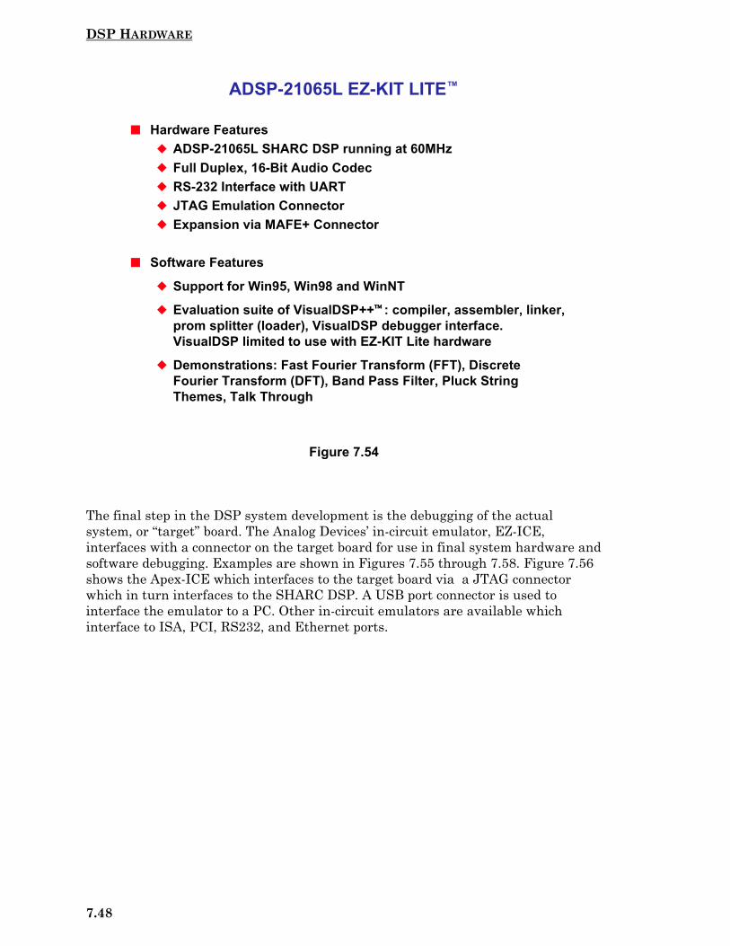
DSP HARDWARE
7.48
Figure 7.54
The final step in the DSP system development is the debugging of the actualsystem, or “target” board. The Analog Devices’ in-circuit emulator, EZ-ICE,interfaces with a connector on the target board for use in final system hardware andsoftware debugging. Examples are shown in Figures 7.55 through 7.58. Figure 7.56shows the Apex-ICE which interfaces to the target board via a JTAG connectorwhich in turn interfaces to the SHARC DSP. A USB port connector is used tointerface the emulator to a PC. Other in-circuit emulators are available whichinterface to ISA, PCI, RS232, and Ethernet ports.
ADSP-21065L EZ-KIT LITE™
� Hardware Features� ADSP-21065L SHARC DSP running at 60MHz� Full Duplex, 16-Bit Audio Codec� RS-232 Interface with UART� JTAG Emulation Connector� Expansion via MAFE+ Connector
� Software Features
� Support for Win95, Win98 and WinNT
� Evaluation suite of VisualDSP++ : compiler, assembler, linker,prom splitter (loader), VisualDSP debugger interface.VisualDSP limited to use with EZ-KIT Lite hardware
� Demonstrations: Fast Fourier Transform (FFT), DiscreteFourier Transform (DFT), Band Pass Filter, Pluck StringThemes, Talk Through
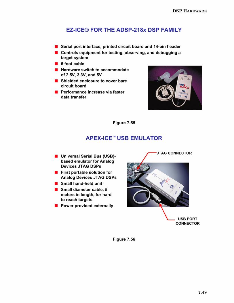
DSP HARDWARE
7.49
Figure 7.55
Figure 7.56
EZ-ICE® FOR THE ADSP-218x DSP FAMILY
� Serial port interface, printed circuit board and 14-pin header� Controls equipment for testing, observing, and debugging a
target system� 6 foot cable� Hardware switch to accommodate
of 2.5V, 3.3V, and 5V� Shielded enclosure to cover bare
circuit board� Performance increase via faster
data transfer
APEX-ICE™ USB EMULATOR
� Universal Serial Bus (USB)-based emulator for AnalogDevices JTAG DSPs
� First portable solution forAnalog Devices JTAG DSPs
� Small hand-held unit� Small diameter cable, 5
meters in length, for hardto reach targets
� Power provided externally
JTAG CONNECTOR
USB PORTCONNECTOR
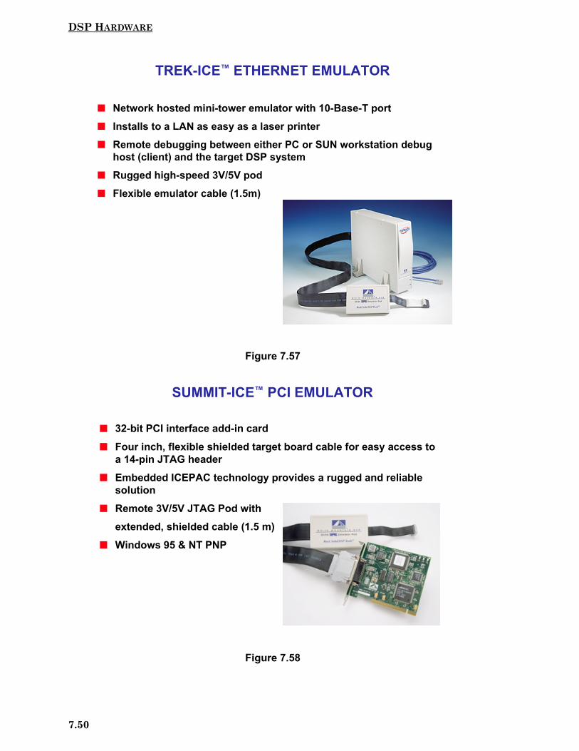
DSP HARDWARE
7.50
Figure 7.57
Figure 7.58
TREK-ICE™ ETHERNET EMULATOR
� Network hosted mini-tower emulator with 10-Base-T port� Installs to a LAN as easy as a laser printer� Remote debugging between either PC or SUN workstation debug
host (client) and the target DSP system� Rugged high-speed 3V/5V pod� Flexible emulator cable (1.5m)
SUMMIT-ICE™ PCI EMULATOR
� 32-bit PCI interface add-in card� Four inch, flexible shielded target board cable for easy access to
a 14-pin JTAG header� Embedded ICEPAC technology provides a rugged and reliable
solution� Remote 3V/5V JTAG Pod with
extended, shielded cable (1.5 m)� Windows 95 & NT PNP
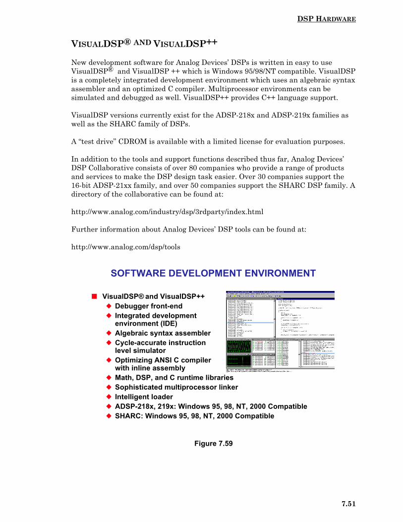
DSP HARDWARE
7.51
VISUALDSP® AND VISUALDSP++
New development software for Analog Devices’ DSPs is written in easy to useVisualDSP® and VisualDSP ++ which is Windows 95/98/NT compatible. VisualDSPis a completely integrated development environment which uses an algebraic syntaxassembler and an optimized C compiler. Multiprocessor environments can besimulated and debugged as well. VisualDSP++ provides C++ language support.
VisualDSP versions currently exist for the ADSP-218x and ADSP-219x families aswell as the SHARC family of DSPs.
A “test drive” CDROM is available with a limited license for evaluation purposes.
In addition to the tools and support functions described thus far, Analog Devices’DSP Collaborative consists of over 80 companies who provide a range of productsand services to make the DSP design task easier. Over 30 companies support the16-bit ADSP-21xx family, and over 50 companies support the SHARC DSP family. Adirectory of the collaborative can be found at:
http://www.analog.com/industry/dsp/3rdparty/index.html
Further information about Analog Devices’ DSP tools can be found at:
http://www.analog.com/dsp/tools
Figure 7.59
SOFTWARE DEVELOPMENT ENVIRONMENT
� VisualDSP® and VisualDSP++� Debugger front-end� Integrated development
environment (IDE)� Algebraic syntax assembler� Cycle-accurate instruction
level simulator� Optimizing ANSI C compiler
with inline assembly� Math, DSP, and C runtime libraries� Sophisticated multiprocessor linker� Intelligent loader� ADSP-218x, 219x: Windows 95, 98, NT, 2000 Compatible� SHARC: Windows 95, 98, NT, 2000 Compatible

DSP HARDWARE
7.52
Figure 7.60
Figure 7.61
VisualDSP® 7.0 FOR ADSP-218x AND ADSP-219x
� Hosted on Windows 95, Windows 98, Windows NT 4.0 with SP3 or later
� ADSP-219x simulator target supports the 219x core
� ELF/DWARF toolset, including compiler with classical andprocessor-specific optimizations
� Tcl command line scripting language
� Support automated test of DSP system
� 21xx Object Translator
� Peripheral Code Wizard supporting 218x and 219x peripherals
VisualDSP++™ FOR SHARC® DSPs
� Supports Windows 95, 98, NT, 2000
� ELF/Dwarf-2 file format enables effective debug operation
� Pre-processor for linker/assembler separate from compiler
� Fast ICE stepping - 0.9 sec. per step
� MultiProcessor (MP) support
� Synchronous run, step, and halt
� Tcl command line scripting language
� Support automated test of DSP system
� Statistical Profiling
� C++ capabilities
� Graphical Plotting
DSP HARDWARE
7.53
Figure 7.62
Figure 7.63
TigerSHARC® DEVELOPMENT TOOLS
� The TigerSHARC architecture is supported by a robust set ofsimulation, code generation, and debug tools that includes:� VisualDSP Integrated Development Environment
� Simulator, Assembler, Loader, Debugger, and Compiler� DSP & Math Libraries
� Emulators – All present ADI JTAG emulators support theTigerSHARC DSP family
� EZ-KIT Lite� Successive VisualDSP revisions will continuously increase
functionality.
VisualDSP TEST DRIVE
� The test drive is a 30-day evaluation of VisualDSP's full package. Itdoes not include a tutorial. The new test drive is a full version ofVisualDSP and contains pdf.'s of the VisualDSP manuals.
� The customer is presented with the test drive CD. The customerthan proceeds to the Analog Devices DSP Tools website, clicks onTest Drive Registrationwww.analog.com/industry/dsp/tools/test_drive.html and registersonline. After they complete the registration process they willreceive a serial number immediately that will allow them to use thetest drive. The test drive will expire 30-days from the install andthey will not be able to register the test drive again.
� The SHARC VisualDSP test drive is now available, SAP part #VDSP-SHARC-PC-TEST.
� The VisualDSP TigerSHARC test drive will be availableSummer 2000
� The VisualDSP ADSP-218x/219x test drive will be available inSeptember 2000

DSP HARDWARE
7.54
Figure 7.64
ADI DSP COLLABORATIVE - WHAT IS IT?
� Over 80 Companies that provide a wide range of products and services to make your design challenge easier
� Architecture Coverage� Over 30 Companies support 16-bit, ADSP-21xx Family� Over 50 Companies support SHARC® DSP Family
� Over 400 Products from the Following Categories:� Algorithms� Real-Time Operating Systems� Debuggers� MATLAB® DSP Support
� Focused Applications :� Audio� Digital Radio� Industrial Inspection & Control� Medical Instrumentation/Imaging� Military/Aerospace
� Motor/Motion Control� Radar/Sonar� Telecom� Video/Sound Processing
� Emulators� Hardware Development Boards� Graphical S/W Programs� Consulting Services
���� http://www.analog.com/industry/dsp/3rdparty/index.html

DSP HARDWARE
7.55
REFERENCES
1. Steven W. Smith, The Scientist and Engineer’s Guide to Digital SignalProcessing, Second Edition, 1999, California Technical Publishing,P.O. Box 502407, San Diego, CA 92150. Also available for free download at:http://www.dspguide.com or http://www.analog.com/industry/dsp/dsp_book
2. C. Britton Rorabaugh, DSP Primer, McGraw-Hill, 1999.
3. Richard J. Higgins, Digital Signal Processing in VLSI, Prentice-Hall,1990.
4. Ethan Bordeaux, Advanced DSP Performance Complicates MemoryArchitecures in Wireless Designs, Wireless Systems Design, April 2000.
5. DSP Designer’s Reference (DSP Solutions) CDROM, Analog Devices,1999.
6. DSP Navigators: Interactive Tutorials about Analog Devices’ DSPArchitectures (Available for ADSP-218x family and SHARC family):http://www.analog.com/industry/dsp/training/index.html#Navigator
7. General DSP Training and Workshops:http://www.analog.com/industry/dsp/training
The following DSP Reference Manuals and documentation are availablefor free download from: http://www.analog.com/industry/dsp/tech_docs.html
8. ADSP-2100 Family Users Manual, 3rd Edition, Sept., 1995.
9. ADSP-2100 Family EZ Tools Manual.
10. ADSP-2100 EZ-KIT Lite Reference Manual.
11. Using the ADSP-2100 Family, Vol. 1, Vol. 2.
12. ADSP-2106x SHARC User’s Manual, 2nd Edition, July, 1996.
13. ADSP-2106x SHARC EZ-KIT Lite Manual.
14. ADSP-21065L SHARC User’s Manual, Sept. 1, 1998.
15. ADSP-21065L SHARC EZ-LAB User’s Manual.
16. ADSP-21160 SHARC DSP Hardware Reference.

DSP HARDWARE
7.56
Related Documents


![HMO2024 - SOS · [HMO2024] HMO1522 [HMO1524], Mixed Signal Mixed Signal 2](https://static.cupdf.com/doc/110x72/606a26e1cd05047284562add/hmo2024-sos-hmo2024-hmo1522-hmo1524-mixed-signal-mixed-signal-2.jpg)