Mixed Mode Simulation – First Steps P. Fischer Lehrstuhl für Schaltungstechnik und Simulation ZITI, Uni Heidelberg (Original slides from Florian Erdinger) VLSI Design - Mixed Mode Simulation © P. Fischer, ZITI, Uni Heidelberg Page 1

Welcome message from author
This document is posted to help you gain knowledge. Please leave a comment to let me know what you think about it! Share it to your friends and learn new things together.
Transcript

Mixed Mode Simulation – First Steps
P. Fischer
Lehrstuhl für Schaltungstechnik und SimulationZITI, Uni Heidelberg
(Original slides from Florian Erdinger)
VLSI Design - Mixed Mode Simulation © P. Fischer, ZITI, Uni Heidelberg Page 1

Why Simulate in Mixed Mode?
§ Most analog circuits need interaction with digital circuits• control logic to steer the analogue part• processing / verification of results
§ Simple digital functionality can be obtained by spice sources (vpulse, vpwl,…), but this is tedious, inflexible,…
§ (More flexibility by using Verilog-A. Good for simple extensions (DAC..), but not suited for large digital parts)
→ Mixed Mode Simulation:§ Digital parts:
• Hardware Description Language (Verilog, VHDL) – very flexible• Digital simulator
§ Analog parts:• Schematics• Analog simulator
VLSI Design - Mixed Mode Simulation © F. Erdinger, ZITI, Uni Heidelberg Page 2

Mixed Mode Simulation
§ Two simulators run in parallel• Digital Simulator for digital part• Analogue simulator for analogue part• Interface Elements translate between both domains
§ Time must be (internally) synchronized
§ Advantages:• Complex steering / logic easy to implement• Much faster simulation in large designs (once it runs…)
§ Drawbacks: More complex. Long simulator startup.
AnalogDomain
Digital Domain
L2E
E2L
VLSI Design - Mixed Mode Simulation
Interface Elements
© F. Erdinger, ZITI, Uni Heidelberg Page 3
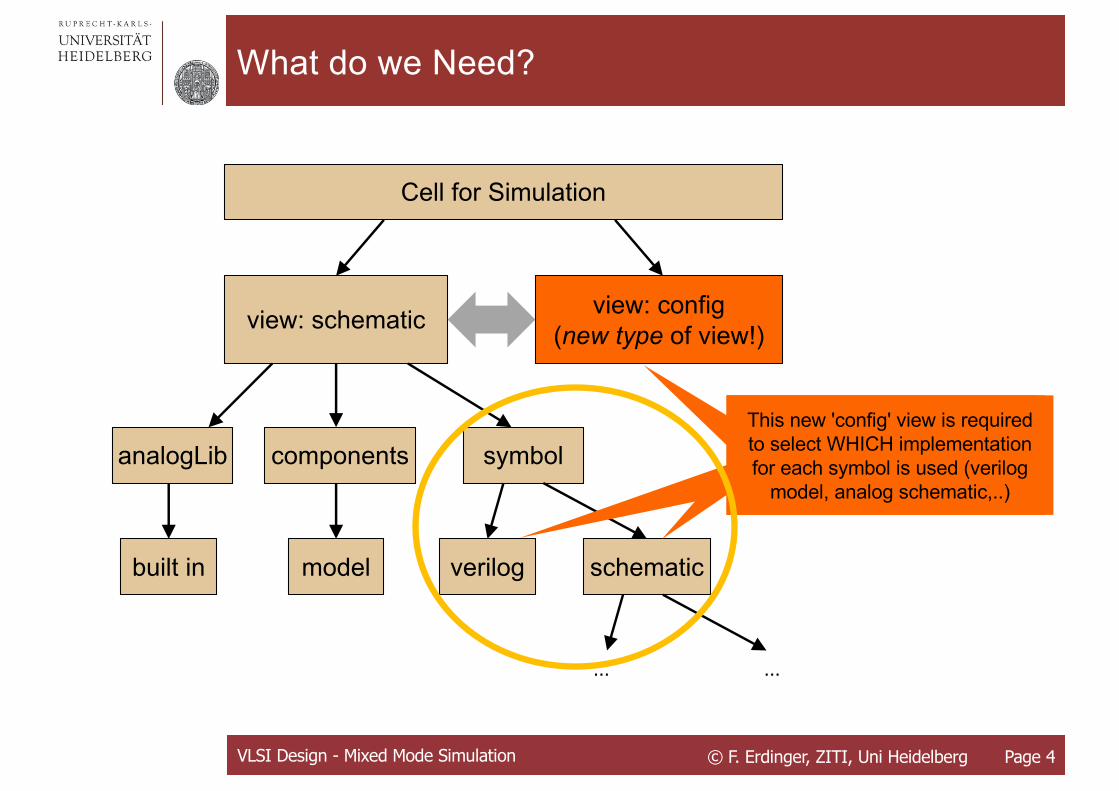
What do we Need?
view: schematic view: config(new type of view!)
Cell for Simulation
verilog
symbolcomponentsanalogLib
schematicmodel
VLSI Design - Mixed Mode Simulation
This new type of view is required to select, WHICH implementation
for a symbol is used (verilog model, analog schematic,..)
This new type of view is required to select, WHICH implementation
for a symbol is used (verilog model, analog schematic,..)
This new 'config' view is required to select WHICH implementationfor each symbol is used (verilog
model, analog schematic,..)
built in
… …
© F. Erdinger, ZITI, Uni Heidelberg Page 4

A SIMPLE EXAMPLE
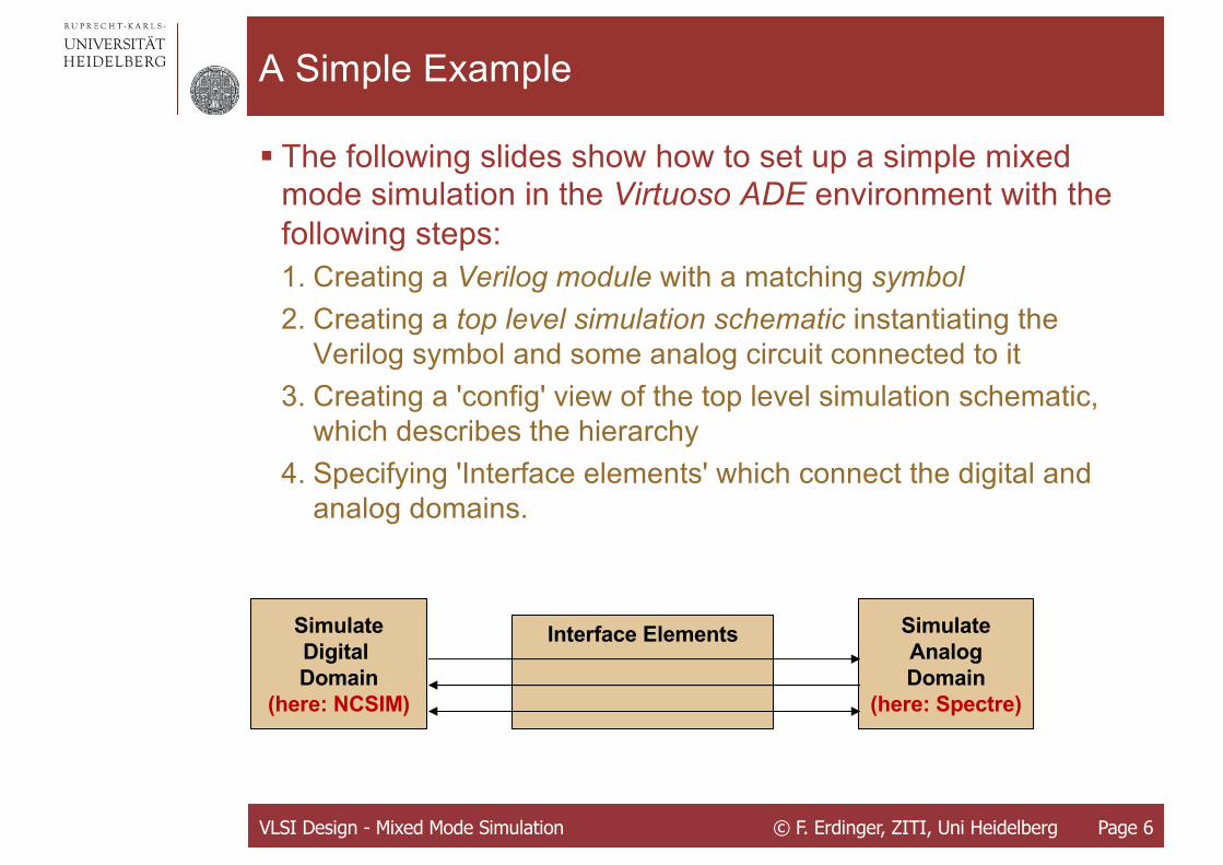
A Simple Example
§ The following slides show how to set up a simple mixed mode simulation in the Virtuoso ADE environment with the following steps:1. Creating a Verilog module with a matching symbol2. Creating a top level simulation schematic instantiating the
Verilog symbol and some analog circuit connected to it3. Creating a 'config' view of the top level simulation schematic,
which describes the hierarchy4. Specifying 'Interface elements' which connect the digital and
analog domains.
VLSI Design - Mixed Mode Simulation
Interface Elements SimulateAnalogDomain
(here: Spectre)
SimulateDigital Domain
(here: NCSIM)
© F. Erdinger, ZITI, Uni Heidelberg Page 6

Before You Start:
§ We need to make the ‘connectlib’ available:
§ In file cds.lib, add the lineDEFINE connectLib/opt/eda/XCELIUM2009/tools.lnx86/affirma_ams/etc/connect_lib/connectLib
§ You can also use the Library Manager:• In the Library Manager: Edit → Add Library Path…• Edit → Add Library • … (name must be connectLib)• Save
§ This must only be done once, library definition is saved in cds.lib
VLSI Design - Mixed Mode Simulation © F. Erdinger, ZITI, Uni Heidelberg Page 7

1. Creating a New Verilog Module
§ In 'Library Manager:• File → New → Cell View• 'Cell': name of verilog module• 'View': 'verilog' (Non-Capital!)• 'Type': Verilog
§ The Cadence text editor opens with a 'naked' Verilog module
VLSI Design - Mixed Mode Simulation © F. Erdinger, ZITI, Uni Heidelberg Page 8

1. Editing the Verilog Module & Creating a Symbol
§ Fill the Verilog module with some code.• The code need not be synthesizable
§ For instanceinitial out = 1'b0;always #10 out <= ~out;
§ When you close the text file,it is automatically parsed.Correct it until there are noerrors left.
§ When the Verilog file is closed, Virtuoso offers to create a symbol if there is none (or modify it if it does not fit to the declared interface). Create the symbol.
VLSI Design - Mixed Mode Simulation © F. Erdinger, ZITI, Uni Heidelberg Page 9

§ In 'Library Manager'• File → New → Cell View• Create a schematic
§ Put an instance of your Verilog module, i.e. the symbol§ If the Verilog contains parameters, the symbol inherits them.
• To see them: In the instantiated symbol, select CDFParameter -> Verilog (not 'Use Tool Filter’)
§ Add some analog circuit (symbols, primitives, sources, ...)§ ‘Digital’ and analog circuits can directly be connected
2. Creating A Top Level Simulation Module
VLSI Design - Mixed Mode Simulation © F. Erdinger, ZITI, Uni Heidelberg Page 10
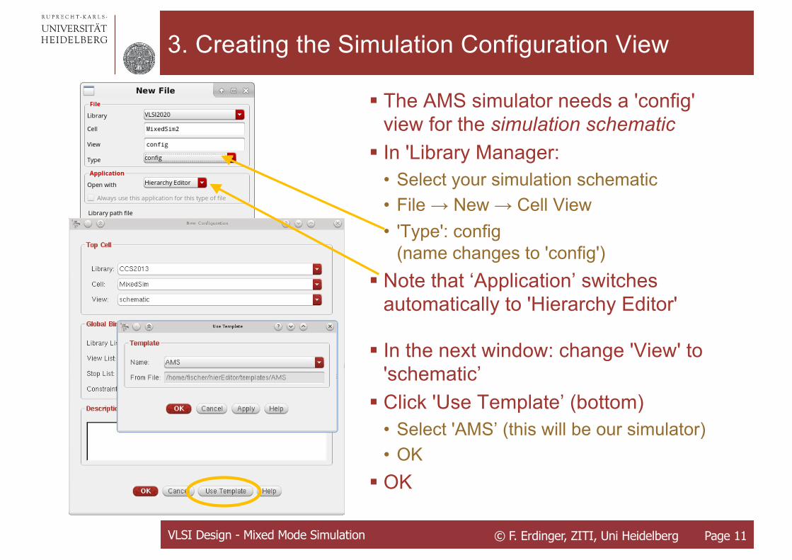
3. Creating the Simulation Configuration View
§ The AMS simulator needs a 'config' view for the simulation schematic
§ In 'Library Manager:• Select your simulation schematic• File → New → Cell View• 'Type': config
(name changes to 'config')§ Note that ‘Application’ switches
automatically to 'Hierarchy Editor'
§ In the next window: change 'View' to 'schematic’
§ Click 'Use Template’ (bottom)• Select 'AMS’ (this will be our simulator)• OK
§ OK
VLSI Design - Mixed Mode Simulation © F. Erdinger, ZITI, Uni Heidelberg Page 11
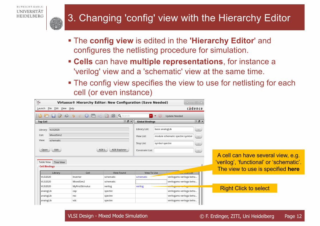
3. Changing 'config' view with the Hierarchy Editor
§ The config view is edited in the 'Hierarchy Editor' and configures the netlisting procedure for simulation.
§ Cells can have multiple representations, for instance a 'verilog' view and a 'schematic' view at the same time.
§ The config view specifies the view to use for netlisting for each cell (or even instance)
VLSI Design - Mixed Mode Simulation © F. Erdinger, ZITI, Uni Heidelberg Page 12
A cell can have several view, e.g. ‘verilog’, ‘functional’ or ‘schematic’.The view to use is specified here
Right Click to select
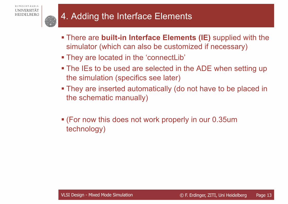
4. Adding the Interface Elements
§ There are built-in Interface Elements (IE) supplied with the simulator (which can also be customized if necessary)
§ They are located in the ‘connectLib’§ The IEs to be used are selected in the ADE when setting up
the simulation (specifics see later)§ They are inserted automatically (do not have to be placed in
the schematic manually)
§ (For now this does not work properly in our 0.35um technology)
VLSI Design - Mixed Mode Simulation © F. Erdinger, ZITI, Uni Heidelberg Page 13
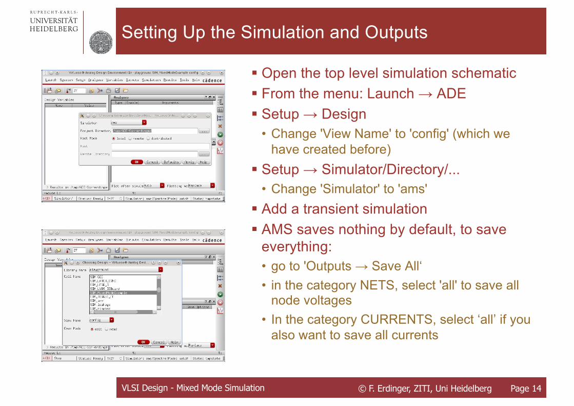
Setting Up the Simulation and Outputs
§ Open the top level simulation schematic§ From the menu: Launch → ADE§ Setup → Design
• Change 'View Name' to 'config' (which we have created before)
§ Setup → Simulator/Directory/...• Change 'Simulator' to 'ams'
§ Add a transient simulation§ AMS saves nothing by default, to save
everything:• go to 'Outputs → Save All‘• in the category NETS, select 'all' to save all
node voltages• In the category CURRENTS, select ‘all’ if you
also want to save all currents
VLSI Design - Mixed Mode Simulation © F. Erdinger, ZITI, Uni Heidelberg Page 14

Specifying the Interface Elements
§ The standard connect rules use 1.8V supply and work fine for UMC018 so nothing has to be really done here... (
§ You can have a look: In the ADE window: select 'Setup → Connect Rules …'
§ There are several 'built-in' interface elements (fast, medium, slow, 1.2V, 3V, …), which can be customized
§ Parameters are: vsup, trise, tfall, rlo, …;à logic levels, driving strength, …
§ Own module can also be specified§ These modules are automatically inserted
in every digital to analog connection in the entire design
)
Choose from the built-in
rules hereUser-
defined rules can be used
VLSI Design - Mixed Mode Simulation © F. Erdinger, ZITI, Uni Heidelberg Page 15

(Viewing and Customizing the Interface Elements)
(This is for information only..)
VLSI Design - Mixed Mode Simulation
To customize or view the rules click here
All interface elements are listed hereThe important ones for us are:
L2E→ Logical to ElectricalE2L→ Electrical to Logical
Select one and click here if you are interested in the code
(Verilog-AMS)
© F. Erdinger, ZITI, Uni Heidelberg Page 16

Using Active Devices
§ If you want to use active devices, like transistors, the models must be defined in Setup->Model Libraries• You may have to pick a ‘section’ (right column)
§ If they are not set, a quick way to get them is:• Save the state of the (ams) simulation to a view
This view is visible in your linux library path under/libname/cellname/ams_state…
• In this cell, there is a file modelSetup.state, which is probably empty (contains nil)
• Copy a ‘modelSetup.state’ file from another simulation state, containing the library paths.
VLSI Design - Mixed Mode Simulation © P. Fischer, ZITI, Uni Heidelberg Page 17

Running and Viewing the Simulation
§ Run the simulation (‘play button’) § In the log file you can see that there are several steps:
• Compilation• Elaboration• Simulation
§ Verilog $display task prints to the log file§ Open the results browser to look at the results:
in the ADE menu: Tools → Results Browser …
§ Select Outputs in the left windows
VLSI Design - Mixed Mode Simulation © F. Erdinger, ZITI, Uni Heidelberg Page 18

Selecting Waveforms
§ To select digital waveforms, open the ‘results browser’ for instance from the schematic window• Right click on command icons -> ADE L Tools• -> You get a pane with 3 entries (calc., res. browser, results)
§ Select Sim->tran->Top• In Verilog Instance, you can select internal variables.
VLSI Design - Mixed Mode Simulation © P. Fischer, ZITI, Uni Heidelberg Page 19
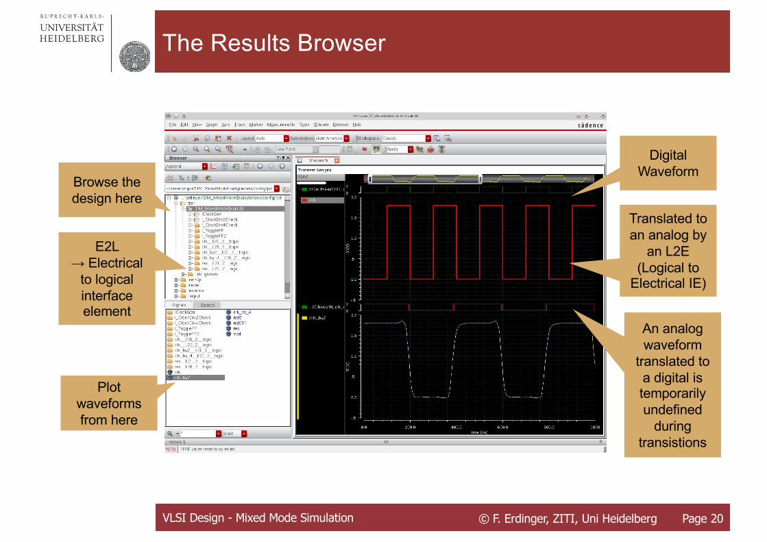
The Results Browser
VLSI Design - Mixed Mode Simulation © F. Erdinger, ZITI, Uni Heidelberg Page 20
Browse the design here
E2L → Electrical
to logical interface element
Digital Waveform
Translated toan analog by
an L2E (Logical to
Electrical IE)
An analog waveform
translated to a digital is temporarily undefined
during transistions
Plot waveforms from here

Sample output
§ Here, The inverter is simulated with its ‚functional‘ model:
§ ‘outinv‘ is a digital signal
VLSI Design - Mixed Mode Simulation © P. Fischer, ZITI, Uni Heidelberg Page 21

Sample output
§ Now, The inverter is simulated with its schematic model:
§ ‘outinv‘ is an analogue signal
VLSI Design - Mixed Mode Simulation © P. Fischer, ZITI, Uni Heidelberg Page 22

EXERCISE: MIXED MODE SIMULATION
Exercise: Clock Generation
§ Step 1: Create a ‘ClockGenerator’ cell• Generate a Verilog view • Use a parameterparameter del=10;to set the clock period. (Parameters can be overwritten in the properties of the symbol. You may have to change the ‘CDF Parameter of view’ combo box to ‘verilog’)
• Follow all steps until you have the symbol§ Step 2: Create a new schematic (for simulation)
• Instantiate the ClockGenerator• Add an inverter or at lease a RC element to do something with
the clock§ Step 3: Mixed mode simulation
• Follow all described steps to setup and run a mixed mode simulation
• Browse through the results
VLSI Design - Mixed Mode Simulation © F. Erdinger, ZITI, Uni Heidelberg Page 24

Exercise: Clock Divider
§ Step 4: Divide by 2:• Create an edge triggered flipflop from two latches (or take if
from a SUSLIB..)• Use it to divide the clock by 2.
§ Step 5: Checking via Verilog: ‘ClockChecker’ cell• Make a Verilog module which has a clock output and an input
for the divided clock • Use Verilog code to verify that the clock is divided correctly
§ NOTE: When re-running the simulation, the results in the lower hierarchy might be missing despite for ‘save all’.→ Closing and re-opening the results browser should fix this.
VLSI Design - Mixed Mode Simulation © F. Erdinger, ZITI, Uni Heidelberg Page 25
Related Documents


