Minimum Reactive Power Filter Design for High Power Converters. Alex-Sander Amavel Luiz * and Braz Jesus Cardoso Filho † * CEFET-MG/Department of Electrical Engineering, Belo Horizonte-MG, Brazil, e-mail: [email protected] † UFMG/Department of Electrical Engineering, Belo Horizonte-MG, Brazil, e-mail: [email protected] Abstract— This work proposes and evaluates an optimized filter design for high power converter with sinusoidal voltage and current. The inherent low switching frequency of this class of converters complicates the filter design and generally results in large filter components. The proposed design culminates in minimum filter reactive power, size and cost. Simulation and experimental results support those ideas. Keywords— High Voltage power converters, Passive filter, Harmonics, Power factor correction. I. INTRODUCTION Many harmonic related issues have been reported recently [1] and [2]. They include excessive heating and losses in electrical machines and other electromagnetic equipments, winding over voltages, reduction of device life service and other problems. Regarding the utility grid, harmonics deteriorate the supplied voltage waveform and increase the electromagnetic emissions. On the other hand, sinusoidal voltage and current in an electrical system is highly desirable. Nevertheless, electronic apparatuses distort the grid current and voltage. In many works, passive sinusoidal filters come out as good alternative to reduce the system harmonic content. The inherently low switching frequency of high power converters, limited from about 500 to 1000 Hz, complicates filter design, which generally results in large filter elements. Besides, due to grid resonance problems and poor filter attenuation the lower the switching frequency the more complex the filter design and worse filter performance are. Unfortunately in literature [2]-[8] only a small number of papers is devoted to multilevel structures ([2], [6] and [7]) and a number even smaller discusses the problem of filter design under very low switching frequency conditions. Still in this case design criteria result again in bulky filter components. This paper proposes an enhanced passive filter configuration for high power converters. A complete filter design based on the optimization of the filter reactive power leads minimum cost weight and size. Besides, reasonably simple design steps culminate in unique and well-defined filter element values. The modulation strategy adopted in this paper is the Selective Harmonic Elimination-SHEPWM, which also results in simplifications on the filter design rules. Moreover, the modulator SHEPWM works under a classical voltage oriented synchronous reference frame control for a high power active rectifier. Simulation and experimental results confirm that it is possible to achieve high power factor operation with low harmonic distortion and satisfactory system performance under very low switching frequency conditions. II. SELECTIVE HARMONIC ELIMINATION. The power circuits in this paper consist of a Neutral Point Clamped-NPC converter working as active rectifier and a passive sinusoidal input filter. References [9]-[11] discuss the generalized method of Selective Harmonic Elimination and state that an arbitrary number M of harmonic can be controlled and/or eliminated from a standard three level output voltage waveform if it is chopped M times per half fundamental period. Expanding the waveform into Fourier series and assuming odd quarter-wave symmetry, the cosine components vanish and (1) gives n th harmonic coefficient of the sine components, (n = 1, 3, 5…). ( ) ( ) ( ) k + k M = k n n n E = a cos . 1 / 4 1 1 ⋅ − 2 / 0 1 < < < M 2 ≤ (1) In order to control the fundamental component and eliminate (M-1) harmonics it is essential to solve a nonlinear and transcendental system of equations. Based on the algorithm in [9] it was developed a computer program to solve those equations intending to control the converter fundamental component and eliminate 5 th and 7 th harmonics. III. SINUSOIDAL FILTER. The sinusoidal input filter topology studied in this work takes up the classical concepts of harmonic filters from electric power systems together with a common solution for VSC active rectifiers [3]-[5]. Previous papers employed similar ideas in power electronics, but they recently reappeared under a high switching frequency modulation condition for a low power drive, [1]. The filter configuration in this work consists of a third order LCL filter plus some harmonic traps as in Fig. 1. A. Minimum Reactive Power Optimized Filter Design. Elementary filter theory recommends that the filter cut-off frequency f co must be placed between the maximum desirable fundamental frequency f 1 and the first non-eliminated harmonic frequency f D with separation factors between each one of them of at least 10. It results in a frequency separation equal to or greater than 100 between f 1 and f D . This is difficult to achieve 1368 978-1-4244-1742-1/08/$25.00 c 2008 IEEE

Welcome message from author
This document is posted to help you gain knowledge. Please leave a comment to let me know what you think about it! Share it to your friends and learn new things together.
Transcript
Minimum Reactive Power Filter Design for High Power Converters.
Alex-Sander Amavel Luiz* and Braz Jesus Cardoso Filho†
* CEFET-MG/Department of Electrical Engineering, Belo Horizonte-MG, Brazil, e-mail: [email protected]† UFMG/Department of Electrical Engineering, Belo Horizonte-MG, Brazil, e-mail: [email protected]
Abstract— This work proposes and evaluates an optimized filter design for high power converter with sinusoidal voltage and current. The inherent low switching frequency of this class of converters complicates the filter design and generally results in large filter components. The proposed design culminates in minimum filter reactive power, size and cost. Simulation and experimental results support those ideas.
Keywords— High Voltage power converters, Passive filter, Harmonics, Power factor correction.
I. INTRODUCTION
Many harmonic related issues have been reported recently [1] and [2]. They include excessive heating and losses in electrical machines and other electromagnetic equipments, winding over voltages, reduction of device life service and other problems. Regarding the utility grid, harmonics deteriorate the supplied voltage waveform and increase the electromagnetic emissions. On the other hand, sinusoidal voltage and current in an electrical system is highly desirable. Nevertheless, electronic apparatuses distort the grid current and voltage.
In many works, passive sinusoidal filters come out as good alternative to reduce the system harmonic content. The inherently low switching frequency of high power converters, limited from about 500 to 1000 Hz, complicates filter design, which generally results in large filter elements. Besides, due to grid resonance problems and poor filter attenuation the lower the switching frequency the more complex the filter design and worse filter performance are. Unfortunately in literature [2]-[8] only a small number of papers is devoted to multilevel structures ([2], [6] and [7]) and a number even smaller discusses the problem of filter design under very low switching frequency conditions. Still in this case design criteria result again in bulky filter components.
This paper proposes an enhanced passive filter configuration for high power converters. A complete filter design based on the optimization of the filter reactive power leads minimum cost weight and size. Besides, reasonably simple design steps culminate in unique and well-defined filter element values. The modulation strategy adopted in this paper is the Selective Harmonic Elimination-SHEPWM, which also results in simplifications on the filter design rules. Moreover, the modulator SHEPWM works under a classical voltage oriented synchronous reference frame control for a high power active rectifier. Simulation and experimental
results confirm that it is possible to achieve high power factor operation with low harmonic distortion and satisfactory system performance under very low switching frequency conditions.
II. SELECTIVE HARMONIC ELIMINATION.The power circuits in this paper consist of a Neutral
Point Clamped-NPC converter working as active rectifier and a passive sinusoidal input filter. References [9]-[11] discuss the generalized method of Selective Harmonic Elimination and state that an arbitrary number M of harmonic can be controlled and/or eliminated from a standard three level output voltage waveform if it is chopped M times per half fundamental period. Expanding the waveform into Fourier series and assuming odd quarter-wave symmetry, the cosine components vanish and (1) gives nth harmonic coefficient of the sine components, (n = 1, 3, 5…).
( ) ( ) ( )k+k
M
=kn nnE=a cos.1/4 1
1
⋅−
2/0 1 <<< M2≤
(1)
In order to control the fundamental component and eliminate (M-1) harmonics it is essential to solve a nonlinear and transcendental system of equations. Based on the algorithm in [9] it was developed a computer program to solve those equations intending to control the converter fundamental component and eliminate 5th and 7th harmonics.
III. SINUSOIDAL FILTER.The sinusoidal input filter topology studied in this
work takes up the classical concepts of harmonic filters from electric power systems together with a common solution for VSC active rectifiers [3]-[5]. Previous papers employed similar ideas in power electronics, but they recently reappeared under a high switching frequency modulation condition for a low power drive, [1].
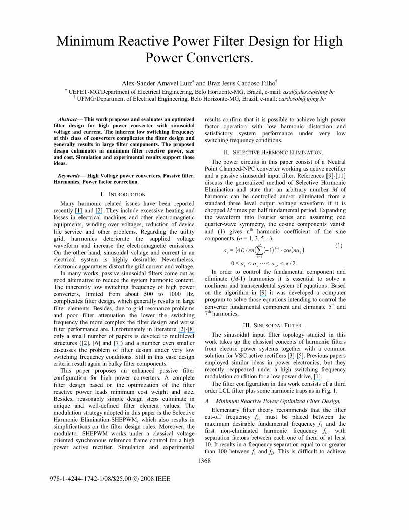
The filter configuration in this work consists of a third order LCL filter plus some harmonic traps as in Fig. 1.
A. Minimum Reactive Power Optimized Filter Design. Elementary filter theory recommends that the filter
cut-off frequency fco must be placed between the maximum desirable fundamental frequency f1 and the first non-eliminated harmonic frequency fD with separation factors between each one of them of at least 10. It results in a frequency separation equal to or greater than 100 between f1 and fD. This is difficult to achieve
1368
978-1-4244-1742-1/08/$25.00 c© 2008 IEEE
with practically all modulation methods under low switching frequency conditions. For this reason, this work suggests a separation between f1 and fD of about 10 in the following way: - The separation between f1 and fco must be greater than 5. - The separation nscd between fco and fD should be about 2.
Then it is possible to find out filter elements. The cut-off frequency can be generically expressed by:
yxco CL=f /1 (2)
This expression leads to an infinite set of pair of values of Lx and Cy, which simultaneously suits this equation for a given value of fco It requires new constraints to solve this problem. Various guidelines for filter design are presented in literature, [5]-[7] and [12], but they are either not feasible for low switching frequency applications or not enough restrictive to come up with a specific solution to the problem.
In [7] in order to limit the converter current ripple iripthe converter side inductor Lc is given by:
ripcc ifUL 64/1≤ (3)
At rated voltage, commutation frequency fc = 180Hz and irip = 10% this results in Lc < 34%. Yet it provides a wide set possible element values. In [12], all filter inductors should be below 10%, which is not practical for many low switching frequency applications. Reference [6] restricts all filter inductors below 10% and imposes Cf = 5%, but the switching frequency is as high as 2.5 kHz. Reference [5] limits all inductors below 10% and Cfbelow 5%, but again the switching frequency is high, fsw = 5-8 kHz.
The filter design optimization can be performed writing an algebraic expression for the total filter reactive power as a function of all reactive elements. This expression under the constraint of (2) represents the optimizing cost function by:
( ) ( )j1irrt C,,C,L,,Lf=kVAQ ......1(4)
The first derivative of Qrt equated to zero leads to the cost function critical points (maximums and minimums):
( ) 0......1 =C,,C,L,,Lf=dLdQ j1i'
xrt(5)
The second derivative of Qrt leads to the cost function inflexions and concavity:
( )j1i''2
xrt C,,C,L,,Lf=dLQd ......12 (6)
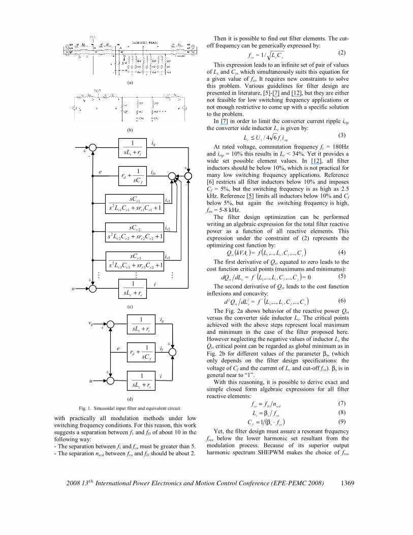
The Fig. 2a shows behavior of the reactive power Qrtversus the converter side inductor Lc. The critical points achieved with the above steps represent local maximum and minimum in the case of the filter proposed here. However neglecting the negative values of inductor Lc the Qrt critical point can be regarded as global minimum as in Fig. 2b for different values of the parameter βs, (which only depends on the filter design specifications: the voltage of Cf and the current of Lc and cut-off fco). βs is in general near to “1”.
With this reasoning, it is possible to derive exact and simple closed form algebraic expressions for all filter reactive elements:
scdDco nff = (7)
cosc fL β= (8)( )cosf fC ⋅β= 1 (9)
Yet, the filter design must assure a resonant frequency fres below the lower harmonic set resultant from the modulation process. Because of its superior output harmonic spectrum SHEPWM makes the choice of fres
(a)
(b)
122222
2
++ rrrr
r
CsrCLssC ir2
ir1
111112
1
++ rrrr
r
CsrCLssC
133332
3
++ rrrr
r
CsrCLssC ir3
+-
e ifo
ig
fd sC
r 1+
tt rsL +1
+
--
cc rsL +1
u+
-
-
i
- - -
(c)
vg
cc rsL +1
u
+
+
+
-
e if
ig
fd sC
r 1+
tt rsL +1
i
(d)
Fig. 1. Sinusoidal input filter and equivalent circuit.
2008 13th International Power Electronics and Motion Control Conference (EPE-PEMC 2008) 1369
easier than other classical modulator, [8] and [11]. This work suggests the expression for fres:
( )[ ] 2ceil coDres fff += , (10)
which intuitively allocates fres between fco and fD. Then: ( )cresseq LfL ⋅β= 22 (11)
( ) ( )[ ] geqceqcf LLLLLL −−⋅= (12)Fig. 3 represents a summary of the MRP-OFD and
produces the element values presented in Table I and II. It is remarkable that the MRP-OFD results in all main filter elements about 15% with fc = 180Hz and fc = 420Hz.
Filter damping is another important designing aspect. Again, the literature presents various different recommendations, [1], [3], [5], [13]-[17]. In [13] the filter is over damped. Reference [14] designs its filter with critical damping. In contrast to them, [1] shows that under damped filters present better attenuation. Following this line [5] adopts filter quality factors Q = 1.8 and 3.6, and [3] chooses Q = 7.7. Additionally [15]-[17] discusses many alternative for resistive damping process, but according to [17] the better one consists in placing the damping resistor in series with capacitor Cf. It is recognizable that passive damping has many collateral effects over the filter. One of them is deterioration in
filter attenuation. This is reasonably compensated by the addition of series resonant harmonic traps in parallel to the shunt branch of Cf. The number of resonant traps depends on the desired system specification and they should be tuned in the first non-eliminated harmonic frequencies. Each branch has to be designed individually with the MRP-OFD to achieve minimum total filter reactive power. They also must be very selective, (Q > 10). Reduction in system efficiency is another trouble of
TABLE I MINIMUM REACTIVE POWER OPTIMIZED FILTER DESIGN.
fc fD fco fres
180Hz 660Hz 390Hz 540Hz 3.0pu 11.0pu 6.5pu 9.0pu 420Hz 1380Hz 815Hz 1110Hz 7.0pu 23.0pu 13.6pu 18.5pu
TABLE II RATINGS OF SINUSOIDAL FILTER ELEMENTS.
(Ubase = 4160V, Sbase = 5MVA, βS = 1).
fc (Hz) Lc Lf Cf
180Hz 1.4123mH 1.3103mH 117.92μF0.15385pu 0.14274pu 0.15385pu
420Hz 0.67543mH 0.56245 mH 56.398μF0.07358pu 0.06127pu 0.07358pu
Lg = 0,025 pu, Lg = 0,22949 mH.
(a)
(b) Fig. 3. Optimized filter design, a) fc = 180Hz and b) fc = 420Hz.
(a)
(b) Fig. 2. Total Reactive power behavior as function of the converter side
inductor and the parameter βs.
1370 2008 13th International Power Electronics and Motion Control Conference (EPE-PEMC 2008)
passive damping. However if there is enough control bandwidth active damping can solve the two difficulty presented. On the contrary, this paper suggests a hybrid solution involving both passive and active damping.
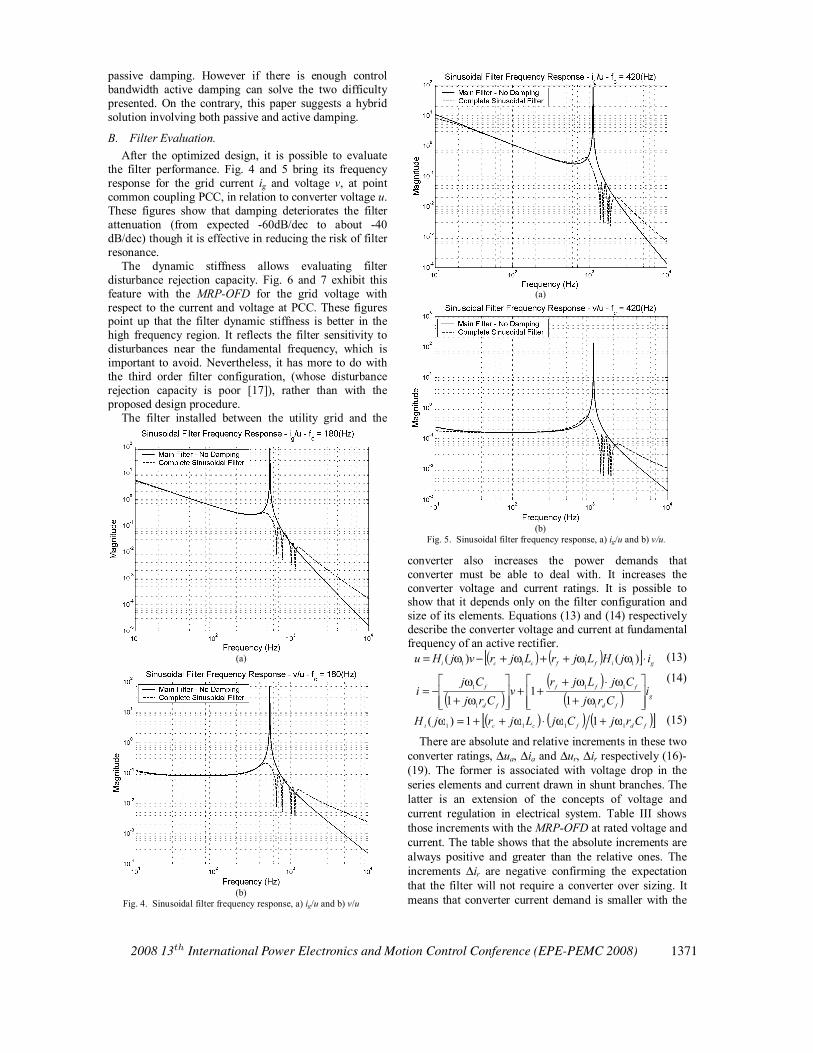
B. Filter Evaluation. After the optimized design, it is possible to evaluate
the filter performance. Fig. 4 and 5 bring its frequency response for the grid current ig and voltage v, at point common coupling PCC, in relation to converter voltage u.These figures show that damping deteriorates the filter attenuation (from expected -60dB/dec to about -40 dB/dec) though it is effective in reducing the risk of filter resonance.
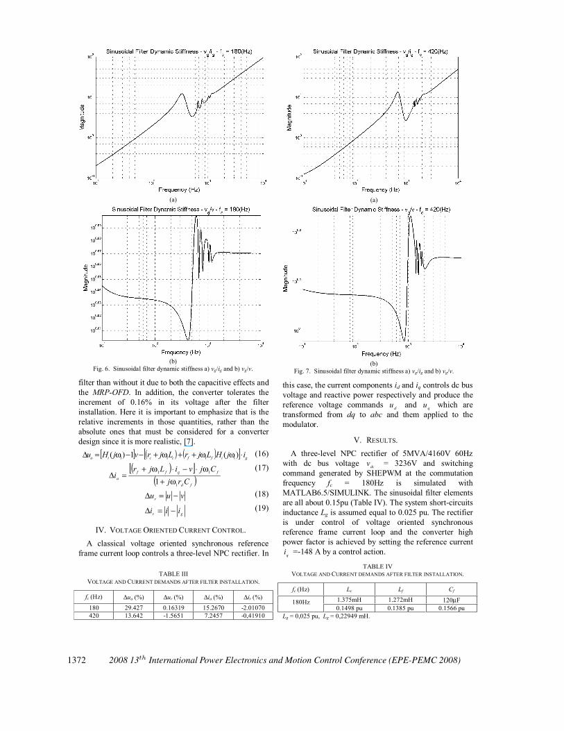
The dynamic stiffness allows evaluating filter disturbance rejection capacity. Fig. 6 and 7 exhibit this feature with the MRP-OFD for the grid voltage with respect to the current and voltage at PCC. These figures point up that the filter dynamic stiffness is better in the high frequency region. It reflects the filter sensitivity to disturbances near the fundamental frequency, which is important to avoid. Nevertheless, it has more to do with the third order filter configuration, (whose disturbance rejection capacity is poor [17]), rather than with the proposed design procedure.
The filter installed between the utility grid and the
converter also increases the power demands that converter must be able to deal with. It increases the converter voltage and current ratings. It is possible to show that it depends only on the filter configuration and size of its elements. Equations (13) and (14) respectively describe the converter voltage and current at fundamental frequency of an active rectifier.
( ) ( )[ ] giffcci ijHLjrLjrvjHu ⋅ωω++ω+−ω= )()( 1111(13)
( )( )
( ) gfd
fff
fd
f iCrj
CjLjrv
CrjCj
iω+
ω⋅ω+++
ω+ω
−=1
11
1
1
11
1
(14)
( ) ( ) ( )[ ]fdfcci CrjCjLjrjH 1111 11)( ω+ω⋅ω++=ω (15)
There are absolute and relative increments in these two converter ratings, Δua, Δia and Δur, Δir respectively (16)-(19). The former is associated with voltage drop in the series elements and current drawn in shunt branches. The latter is an extension of the concepts of voltage and current regulation in electrical system. Table III shows those increments with the MRP-OFD at rated voltage and current. The table shows that the absolute increments are always positive and greater than the relative ones. The increments Δir are negative confirming the expectation that the filter will not require a converter over sizing. It means that converter current demand is smaller with the
(a)
(b) Fig. 5. Sinusoidal filter frequency response, a) ig/u and b) v/u.
(a)
(b) Fig. 4. Sinusoidal filter frequency response, a) ig/u and b) v/u
2008 13th International Power Electronics and Motion Control Conference (EPE-PEMC 2008) 1371
filter than without it due to both the capacitive effects and the MRP-OFD. In addition, the converter tolerates the increment of 0.16% in its voltage after the filter installation. Here it is important to emphasize that is the relative increments in those quantities, rather than the absolute ones that must be considered for a converter design since it is more realistic, [7].
[ ] ( ) ( )[ ] giffccia ijHLjrLjrvjHu ⋅ωω++ω+−−ω=Δ )(1)( 1111(16)
( )[ ]( )fd
fgffa Crj
CjviLjri
1
11
1 ω+ω⋅−⋅ω+
=Δ(17)
vuur −=Δ (18)
gr iii −=Δ (19)
IV. VOLTAGE ORIENTED CURRENT CONTROL.A classical voltage oriented synchronous reference
frame current loop controls a three-level NPC rectifier. In
this case, the current components id and iq controls dc bus voltage and reactive power respectively and produce the reference voltage commands du and qu which are transformed from dq to abc and them applied to the modulator.
V. RESULTS.A three-level NPC rectifier of 5MVA/4160V 60Hz
with dc bus voltage dcv = 3236V and switching command generated by SHEPWM at the commutation frequency fc = 180Hz is simulated with MATLAB6.5/SIMULINK. The sinusoidal filter elements are all about 0.15pu (Table IV). The system short-circuits inductance Lg is assumed equal to 0.025 pu. The rectifier is under control of voltage oriented synchronous reference frame current loop and the converter high power factor is achieved by setting the reference current
qi =-148 A by a control action.
(a)
(b) Fig. 6. Sinusoidal filter dynamic stiffness a) vg/ig and b) vg/v.
(a)
(b) Fig. 7. Sinusoidal filter dynamic stiffness a) vg/ig and b) vg/v.
TABLE III VOLTAGE AND CURRENT DEMANDS AFTER FILTER INSTALLATION.
fc (Hz) Δua (%) Δur (%) Δia (%) Δir (%) 180 29.427 0.16319 15.2670 -2.01070 420 13.642 -1.5651 7.2457 -0,41910
TABLE IV VOLTAGE AND CURRENT DEMANDS AFTER FILTER INSTALLATION.
fc (Hz) Lc Lf Cf
180Hz 1.375mH 1.272mH 120μF0.1498 pu 0.1385 pu 0.1566 pu
Lg = 0,025 pu, Lg = 0,22949 mH.
1372 2008 13th International Power Electronics and Motion Control Conference (EPE-PEMC 2008)
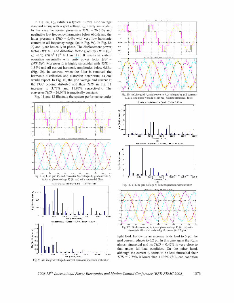
In Fig. 8a, Uab exhibits a typical 3-level Line voltage standard along with a grid voltage Vab nearly sinusoidal. In this case the former presents a THD = 26.61% and negligible low frequency harmonics below 660Hz and the latter presents a THD = 0.4% with very low harmonic content in all frequency range, (as in Fig. 9a). In Fig. 8b Va and ia are basically in phase. The displacement power factor DPF 1 and distortion factor given by DF = (Is1/Is) =1/[( THD)2+1]1/2 1 in [18]. It results in system operation essentially with unity power factor (PF = DPF.DF). Moreover ia is highly sinusoidal with THD = 1.37% and all current harmonic amplitudes below 0.8%, (Fig. 9b). In contrast, when the filter is removed the harmonic distribution and distortion deteriorate, as one would expect. In Fig. 10, the grid voltage and current at the PCC become distorted and their THD in Fig. 11 increase to 3.77% and 11.93% respectively. The converter THD = 26.04% is practically constant.
Fig. 11 and 12 illustrate the system performance under
light load. Following an increase in dc load to 5 pu, the grid current reduces to 0.2 pu. In this case again the Vab is almost sinusoidal and its THD = 0.42% is very close to that under full-load condition. On the other hand, although the current ia seems to be less sinusoidal their THD = 7.79% is lower than 11.93% (full-load condition
Fig. 8. a) Line grid Vab and converter Uab voltages b) grid currents ia,ib, ic and phase voltage Va (in red) with sinusoidal filter.
Fig. 9. a) Line grid voltage b) current harmonic spectrum with filter.
Fig. 10. a) Line grid Vab and converter Uab voltages b) grid currents ia, ib, ic and phase voltage Va (in red) without sinusoidal filter.
(a)
(b)Fig. 11. a) Line grid voltage b) current spectrum without filter.
1
Fig. 12. Grid currents ia, ib, ic and phase voltage Va (in red) with sinusoidal filter and reduced grid current (to 0.2 pu).
2008 13th International Power Electronics and Motion Control Conference (EPE-PEMC 2008) 1373
without filter). The reduced current condition shows that system performance is also satisfactory (DPF ≈ 0.98 and DF ≈ 1.0) resulting in a high power factor operation even under reduced load and switching frequency conditions.
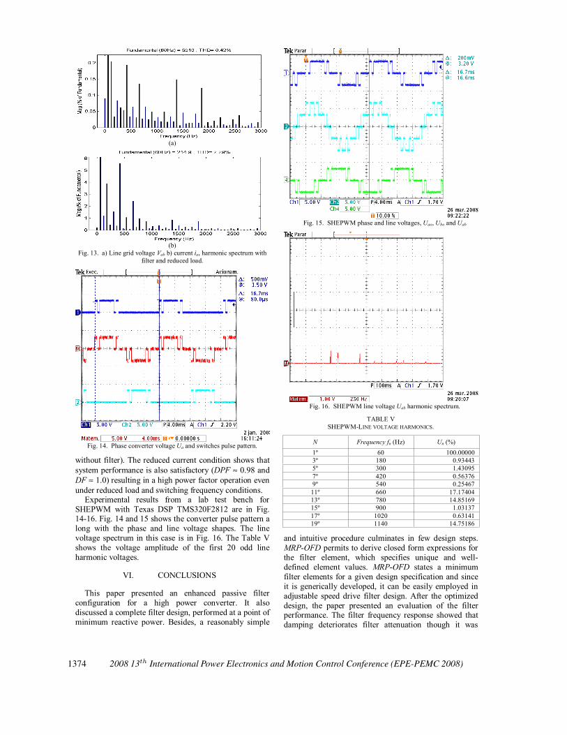
Experimental results from a lab test bench for SHEPWM with Texas DSP TMS320F2812 are in Fig. 14-16. Fig. 14 and 15 shows the converter pulse pattern a long with the phase and line voltage shapes. The line voltage spectrum in this case is in Fig. 16. The Table V shows the voltage amplitude of the first 20 odd line harmonic voltages.
VI. CONCLUSIONS
This paper presented an enhanced passive filter configuration for a high power converter. It also discussed a complete filter design, performed at a point of minimum reactive power. Besides, a reasonably simple
and intuitive procedure culminates in few design steps. MRP-OFD permits to derive closed form expressions for the filter element, which specifies unique and well-defined element values. MRP-OFD states a minimum filter elements for a given design specification and since it is generically developed, it can be easily employed in adjustable speed drive filter design. After the optimized design, the paper presented an evaluation of the filter performance. The filter frequency response showed that damping deteriorates filter attenuation though it was
(a)
(b) Fig. 13. a) Line grid voltage Vab b) current ia, harmonic spectrum with
filter and reduced load.
Fig. 14. Phase converter voltage Ua and switches pulse pattern.
Fig. 15. SHEPWM phase and line voltages, Uao, Ubo and Uab
Fig. 16. SHEPWM line voltage Uab harmonic spectrum.
TABLE V SHEPWM-LINE VOLTAGE HARMONICS.
N Frequency fn (Hz) Un (%) 1º 60 100.00000 3º 180 0.93443 5º 300 1.43095 7º 420 0.56376 9º 540 0.25467 11º 660 17.17404 13º 780 14.85169 15º 900 1.03137 17º 1020 0.63141 19º 1140 14.75186
1374 2008 13th International Power Electronics and Motion Control Conference (EPE-PEMC 2008)
effective in reducing the risk of filter resonance. The addition of harmonic traps in parallel to the shunt branch compensates around the fundamental frequency this loss of attenuation in high frequency region. Besides, this evaluation showed that the filter dynamic stiffness is poor. However it is influenced by the main filter (third order LCL) configuration rather than the proposed design procedure. The paper showed as well that due to capacitive effects and an adequate filter design the converter could tolerate the variations of voltage and current after the filter installation without overrating. The modulation strategy in this paper was the Selective Harmonic Elimination-SHEPWM. The modulator eliminates harmonics up to the 11th. It creates sufficient frequency separation to set cutoff and/or resonance frequencies and simplifies the filter design rules. Furthermore, the modulator SHEPWM worked in a classical voltage oriented synchronous reference frame control of a high power active rectifier. Simulation and experimental results confirmed that it is possible to achieve controllable displacement power factor with low input harmonic distortion and reduced filter kVAr rating with very low switching frequency and, in both full and reduced load conditions.
REFERENCES
[1] Skibinski, G.L.; "A series resonant sinewave output filter for PWM VSI loads" Industry Applications Conference, 2002. 37th IAS Annual Meeting. Conference Record of the Volume 1, 13-18 Oct. 2002 Page(s):247 - 256 vol.1.
[2] Steinke, J.K.; “Use of an LC filter to achieve a motor-friendly performance of the PWM voltage source inverter” IEEE Transactions on Energy Conversion, Vol. 14, No. 3, Sept. 1999, pp.: 649-654.
[3] V. Blasko, V. Kaura, “A novel control to actively damp resonance in input LC filter of a three-phase voltage source converter”, IEEE Trans. on Ind. Applications, Vol. 33, No. 2, 1997, pp. 542-550.
[4] Lindgren and J. Svensson, “Control of a voltage-source converter connected to the grid through an LCL-filter-application to active filter”, in Proc. of PESC 98, May 1998, vol. I, pp. 229-2315.
[5] Liserre, M.; Blaabjerg, F.; Hansen, S.; “Design and control of an LCL-filter-based three-phase active rectifier” IEEE Transactions on Industry Applications, Vol. 41, No. 5, Sept.-Oct. 2005 pp.: 1281 – 1291.
[6] Emilio José Bueno Peña “Optimization of the Behaviour of a NPC Three-Level Converter Connected to the Grid” PhD. Thesis, Universidad de Alcalá, Escuela Politécnica, Departamento de Electrónica, Spain 2005.
[7] Krug, D.; Malinowski, M.; Bernet, S.;"Design and comparison of medium voltage multi-level converters for industry applications" Industry Applications Conference, 2004. 39th IAS Annual Meeting. Conference Record of the 2004 IEEE vol.2, 2004 pp. 781-790.
[8] Rodriguez, J.; Bernet, S.; Bin Wu; Pontt, J.O.; Kouro, S., “Multilevel Voltage-Source-Converter Topologies for Industrial Medium-Voltage Drives”, IEEE Trans. on Ind. Electronics, Vol. 54, No. 6, 2007, pp. 2930-2945.
[9] H. S. Patel and R. G. Hoft, “Generalized techniques of harmonic elimination and voltage control in thyristor inverters: Part I-Harmonic elimination,’’ IEEE Trans. Ind. Applicat., vol. IA-9, no. 3, pp. 310-317, May/June 1973.
[10] H. S. Patel and R. G. Hoft, “Generalized techniques of harmonic elimination and voltage control in thyristor inverters: Part 11-Voltage control techniques,” IEEE Trans. Ind. Applicat., vol. IA-10, no. 5, pp. 666-673, Sept./Oct. 1974.
[11] L.G. Franquelo; J. Napoles; R.C.P. Guisado; J.I. Leon; M.A. Aguirre, “A Flexible Selective Harmonic Mitigation Technique to
Meet Grid Codes in Three-Level PWM Converters”, IEEE Trans. on Ind. Electronics, Vol. 54, No. 6, 2007, pp. 3022-3029.
[12] S. Bernet, S. Ponnaluri, and R. Teichmann, “Design and Loss Comparison of Matrix Converters and Voltage-Source Converters for Modern AC Drives” IEEE Trans. on Industrial Electronics, vol. 49, No. 2, April 2002, pp.: 304-314.
[13] D. A. Rendusara and P. N. Enjeti "An Improved Inverter Output Filter Configuration Reduces Common and Differential Modes at the Motor Terminals in PWM Drive Systems" IEEE Transactions on Power Electronics, Vol. 13, No. 6, November 1998, pp. 1135-1143.
[14] Y. Sozer, D. A. Torrey, and S. Reva, "New Inverter Output Filter Topology for PWM Motor Drives" IEEE Trans. on Power Electronics, Vol. 15, No. 6, pp 1007–1017 Nov. 2000.
[15] P. A. Dahono, “A control method to damp oscillation in the input LC filter of AC-DC PWM converters,” in Proc. PESC’02, June 2002, pp. 1630–1635.
[16] P. A. Dahono; Y. R. Bahar; Y. Sato; T. Kataoka,“Damping of transient oscillations on the output LC filter of PWM inverters by using a virtual resistor” Proceedings of 4th IEEE International Conference on Power Electronics and Drive Systems, PEDS 2001, Indonesia, pp.: 403-407
[17] L. N. Arruda, “Sistema de geração distribuída de energia fotovoltaica” Master degree dissertation, Universidade Federal de Minas Gerais, 1999.
[18] Mohan, N; Underland, T.M.; Robbins, W. P.; "Power Electronics, converters, applications and design", John Wiley & Sons, USA, 1989.
2008 13th International Power Electronics and Motion Control Conference (EPE-PEMC 2008) 1375
Related Documents