Miniature Fiber Bragg Grating Sensor Interrogator (FBG-Transceiver™) System For Use in Aerospace and Automotive Health Monitoring Systems Edgar A. Mendoza, a Cornelia Kempen, a Allan Panahi, a and Craig Lopatin. b a Redondo Optics, Inc., 811 N. Catalina Avenue, Suite 1100, Los Angeles, CA, USA 90277; b Naval Surface Warfare Center, Indian Head Division, Indian Head, MD, USA 20640 ABSTRACT Fiber Bragg grating sensors (FBGs) have gained rapid acceptance in aerospace and automotive structural health monitoring applications for the measurement of strain, stress, vibration, acoustics, acceleration, pressure, temperature, moisture, and corrosion distributed at multiple locations within the structure using a single fiber element. The most prominent advantages of FBGs are: small size and light weight, multiple FBG transducers on a single fiber, and immunity to radio frequency interference. A major disadvantage of FBG technology is that conventional state-of-the-art fiber Bragg grating interrogation systems are typically bulky and heavy bench top instruments that are assembled from off-the-shelf fiber optic and optical components integrated with a signal electronics board into an instrument console. Based on the need for a compact FBG interrogation system, this paper describes recent progress towards the development of a miniature fiber Bragg grating sensor interrogator (FBG-Transceiver™) system based on multi-channel integrated optic sensor (InOSense) microchip technology. The hybrid InOSense microchip technology enables the integration of all of the functionalities, both passive and active, of conventional bench top FBG sensor interrogators systems, packaged in a miniaturized, low power operation, 2-cm x 5-cm small form factor (SFF) package suitable for the long-term structural health monitoring in applications where size, weight, and power are critical for operation. The sponsor of this program is NAVAIR under a DOD SBIR contract. Keywords: Integrated optics, hybrid PLC, fiber sensors, structural health monitoring, nondestructive inspection, aerospace, military, miniature, and ordnance. 1. INTRODUCTION Fiber optic sensors form part of our everyday life and can be found in systems from Mars to Manhattan. One of the most widely used and accepted type of fiber optic sensors is the Fiber Bragg grating (FBG) sensor. FBG sensors are a proven structural health monitoring technology utilized for the in situ monitoring of advanced structures in aviation, aerospace systems, civil structures, and the petrochemical industry. Because of its lightness, micron-size transducers, and immunity to electromagnetic interference, it can be easily casted, embedded, or surface mounted on a structure. The FBG sensors can be produced in glass or plastic optical fiber to meet harsh environmental conditions and structural demands for a variety of applications. The sensor fibers are packaged in strong, rugged materials to withstand harsh environments such as embedded in fiber composite structures, in transatlantic fiber cable installations, tow-array sonar, and missile fiber guiding systems. In addition, it offers the ability to distribute multiple sensors on a single fiber strand. A major drawback of FBG sensor technology is that today’s commercially available FBG sensor interrogation systems are bench- top laboratory instruments that are too bulky and heavy to be permanently installed in aerospace or automobile applications. Because of the need for a compact, low weight, low power FBG interrogation system, Redondo Optics, Inc. under a Navy sponsor SBIR program [1] is currently in the process of developing a family of miniature FBG interrogation (FBG- Transceiver™) systems that uses ROI’s proprietary integrated optic sensor (InOSense™) microchip technology as an optical bench to integrate all the functionalities of the key passive and active optoelectronics components of conventional FBG interrogation systems, such as the light guides, splitters and couplers, light source, photodetectors, wavelength Photonics in the Transportation Industry: Auto to Aerospace edited by Alex A. Kazemi, Christopher S. Baldwin, Proc. of SPIE Vol. 6758 67580B, (2007) · 0277-786X/07/$18 · doi: 10.1117/12.752002 Proc. of SPIE Vol. 6758 67580B-1

Welcome message from author
This document is posted to help you gain knowledge. Please leave a comment to let me know what you think about it! Share it to your friends and learn new things together.
Transcript
Miniature Fiber Bragg Grating Sensor Interrogator
(FBG-Transceiver™) System For Use in Aerospace and Automotive
Health Monitoring Systems
Edgar A. Mendoza,a Cornelia Kempen,
a Allan Panahi,
a and Craig Lopatin.
b
aRedondo Optics, Inc., 811 N. Catalina Avenue, Suite 1100, Los Angeles, CA, USA 90277;
bNaval Surface Warfare Center, Indian Head Division, Indian Head, MD, USA 20640
ABSTRACT
Fiber Bragg grating sensors (FBGs) have gained rapid acceptance in aerospace and automotive structural health
monitoring applications for the measurement of strain, stress, vibration, acoustics, acceleration, pressure, temperature,
moisture, and corrosion distributed at multiple locations within the structure using a single fiber element. The most
prominent advantages of FBGs are: small size and light weight, multiple FBG transducers on a single fiber, and
immunity to radio frequency interference. A major disadvantage of FBG technology is that conventional state-of-the-art
fiber Bragg grating interrogation systems are typically bulky and heavy bench top instruments that are assembled from
off-the-shelf fiber optic and optical components integrated with a signal electronics board into an instrument console.
Based on the need for a compact FBG interrogation system, this paper describes recent progress towards the
development of a miniature fiber Bragg grating sensor interrogator (FBG-Transceiver™) system based on multi-channel
integrated optic sensor (InOSense) microchip technology. The hybrid InOSense microchip technology enables the
integration of all of the functionalities, both passive and active, of conventional bench top FBG sensor interrogators
systems, packaged in a miniaturized, low power operation, 2-cm x 5-cm small form factor (SFF) package suitable for the
long-term structural health monitoring in applications where size, weight, and power are critical for operation. The
sponsor of this program is NAVAIR under a DOD SBIR contract.
Keywords: Integrated optics, hybrid PLC, fiber sensors, structural health monitoring, nondestructive inspection,
aerospace, military, miniature, and ordnance.
1. INTRODUCTION
Fiber optic sensors form part of our everyday life and can be found in systems from Mars to Manhattan. One of the most
widely used and accepted type of fiber optic sensors is the Fiber Bragg grating (FBG) sensor. FBG sensors are a proven
structural health monitoring technology utilized for the in situ monitoring of advanced structures in aviation, aerospace
systems, civil structures, and the petrochemical industry. Because of its lightness, micron-size transducers, and
immunity to electromagnetic interference, it can be easily casted, embedded, or surface mounted on a structure. The FBG
sensors can be produced in glass or plastic optical fiber to meet harsh environmental conditions and structural demands
for a variety of applications. The sensor fibers are packaged in strong, rugged materials to withstand harsh environments
such as embedded in fiber composite structures, in transatlantic fiber cable installations, tow-array sonar, and missile
fiber guiding systems. In addition, it offers the ability to distribute multiple sensors on a single fiber strand. A major
drawback of FBG sensor technology is that today’s commercially available FBG sensor interrogation systems are bench-
top laboratory instruments that are too bulky and heavy to be permanently installed in aerospace or automobile
applications.
Because of the need for a compact, low weight, low power FBG interrogation system, Redondo Optics, Inc. under a
Navy sponsor SBIR program[1]
is currently in the process of developing a family of miniature FBG interrogation (FBG-
Transceiver™) systems that uses ROI’s proprietary integrated optic sensor (InOSense™) microchip technology as an
optical bench to integrate all the functionalities of the key passive and active optoelectronics components of conventional
FBG interrogation systems, such as the light guides, splitters and couplers, light source, photodetectors, wavelength
Photonics in the Transportation Industry: Auto to Aerospaceedited by Alex A. Kazemi, Christopher S. Baldwin, Proc. of SPIE Vol. 6758
67580B, (2007) · 0277-786X/07/$18 · doi: 10.1117/12.752002
Proc. of SPIE Vol. 6758 67580B-1
demultiplexing filters, FBG sensor signal demodulators, and signal processing IC-electronics packaged in a miniaturized,
environmentally qualified, hermetically sealed 2-cm x 2-cm x 5-cm single fiber FBG-Transceiver™ system suitable for
the in-situ installation and long term operation in aerospace, automotive, and industrial applications where size, weight,
and power consumption are a critical requirement for the installation of structural health monitoring systems.
2. THE FBG-TRANSCEIVER™ SYSTEM
The FBG-Transceiver™ system is a compact, multi-channel FBG sensor interrogation unit that uses ROI’s proprietary
integrated optic sensor (InOSense™) microchip technology as an optical bench to integrate the functionality of all of the
key passive and active optoelectronics components such as the light guides, splitters and couplers, light source,
photodetectors, wavelength demultiplexing, FBG sensor signal demodulators, and signal processing IC-electronics of
conventional bench-top FBG sensor interrogators in a miniaturized, telecommunications standard, small form factor
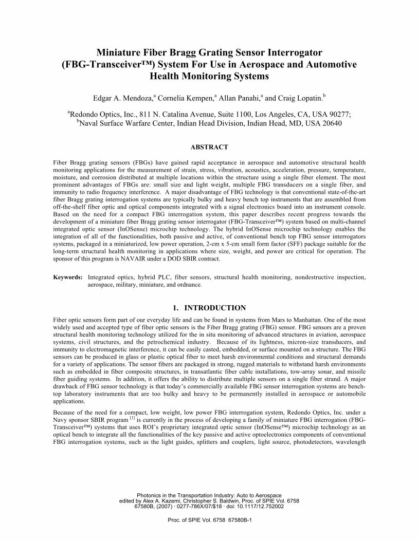
single fiber package. The FBG-Transceiver™ unit, shown in Figure 1, is a bi-directional, transmit and receive, FBG
transducer communications unit that uses the principle of wavelength division demultiplexing (WDDM), commonly used
in WDM telecommunication networks, to separate each of the received FBG sensor signals and interrogate the status of
each of the individual sensors in an array of (1 to 40) FBG transducers distributed along a single optical fiber in real
time.[2]
Fig. 1 ROI’s family of single channel, five-channel, and twelve-channel integrated optic FBG interrogation
(FBG-Transceiver™) devices.
Proc. of SPIE Vol. 6758 67580B-2
The principle of operation of an FBG sensor is based on the environmentally induced wavelength shift, associated with
changes in stress-strain, temperature, vibration, pressure, etc., of the active peak wavelength of the grating that is
attached to the structure under evaluation. ROI uses a passive demodulation technique, based on dispersive filter
structure, in which the wavelength encoded optical signature of each of the FBG transducers in the array is transformed
into an electrical signal at each of the photo receivers by means of the optical properties of the dispersive filter. A
microprocessor controller mounted on a CMOS-PC board processes the transformed electrical signal carrying the
information from each of the FBG sensors, and transmits the process signals to a remote station via a USB data
communication interface. The complete electrical power budget for the FBG-Transceiver™ unit is estimated at
approximately �0.1 Watts, allowing the use of the same USB communications port to provide power to the unit. The
complete InOSense™ microchip and signal processing IC-electronics unit is packaged in a single fiber,
telecommunications grade, small form factor package to produce a miniature multi-channel FBG-Transceiver™ system
that can be used to monitor the status of FBG transducers embedded or surface mounted on the structure. The target
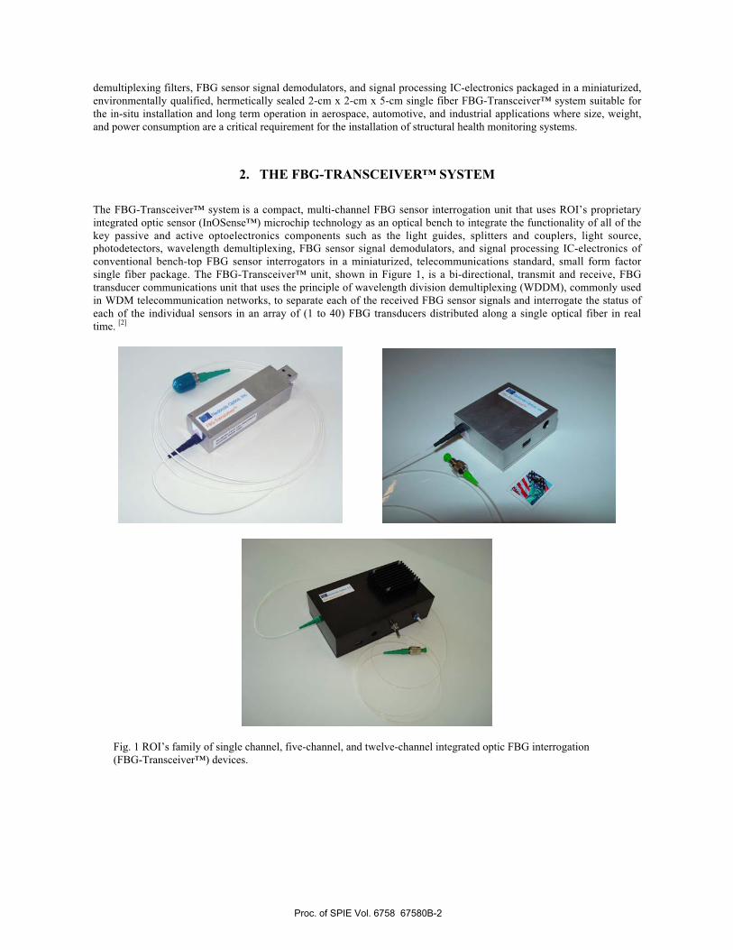
performance specifications of the FBG-Transceiver™ system are shown in Table 1.
Table 1 Target performance specifications of multi-channel FBG-Transceiver™ system.
3. HYBRID INTEGRATED OPTIC SENSOR (INOSENSE™) MICROCHIP
TECHNOLOGY
Planar lightwave circuit (PLC) technology has emerged as the new optical platform of choice for integration and large
scale manufacturing of optical components. The technology draws on the excellent heat-dissipation and mechanical
properties of silicon wafers. Optical component designers use the silicon substrate as an optical bench to integrate
unpackaged optical components, such as lasers, photodiodes, and micro-optic elements in die form, onto the PLC chip
and then re-package the chip in a single unit. Precise micro-machine features on the PLC chip allow the passive
mechanical alignment and attachment of the different opto-electronic components, all accurate enough for reliable
communication between the components and the outside world.
Model No FBGT-100 FBGT-500 FBGT-1200
FBG Sensing Channels 1 5 12
Monitoring Mode
Monitoring Principle
Wavelength Range
Output Power Max (-)0.5 dBm Max 0 dBm Max 5 dBm
Minimum Sensor Spacing
Wavelength Resolution
Wavelength Accuracy
Wavelength Repeatability
Sensor Sampling Rate
Signal Processor
Data Communication
Optical Connector
Data Display
Power Supply
Weight 0.25 ounce 0.5 ounce 1 ounce
Dimensions 18.5 mm x 18.5 mm x 50 mm 55 mm x 55 mm x 20 mm 55 mm x 55 mm x 20 mm
12 V/500 mA
Microcontroller – Sensor calibration and T compensation
USB, Ethernet, Wireless, Bluetooth
FC/APC or Custom
LabView Graphical Interface
1 pm @ 100 Hz
± 1 pm
± 1 pm @ 100 Hz
0.1 Hz to 20 kHz
Stress-strain, temperature, pressure, vibration, and acoustics
Wavelength division demultiplexing (WDDM)
1530 nm to 1580 nm
2 cm
Proc. of SPIE Vol. 6758 67580B-3
A1 A2 An
a10 fl
Peak Wavelength Shillci FBG Sensor @ —1.2 pm / micro-shah
FB6 ReflectionSpectrum0.'
WDM Filter(Edge or Bandpass)
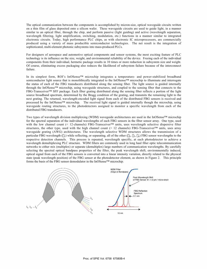
The optical communication between the components is accomplished by micron-size, optical waveguide circuits written
on a thin film of glass deposited onto a silicon wafer. These waveguide circuits are used to guide light, in a manner
similar to an optical fiber, through the chip, and perform passive (light guiding) and active (wavelength separation,
wavelength filtering, light amplification, switching, modulation, etc.) functions in a manner similar to integrated
electronic circuits. Today, high performance PLC chips, as with electronic IC microprocessors, are commercially
produced using a variety of mass producible semiconductor technologies. The net result is the integration of
sophisticated, multi-element photonic subsystems into mass-produced PLCs.
For designers of aerospace and automotive optical components and sensor systems, the most exciting feature of PLC
technology is its influence on the size, weight, and environmental reliability of the device. Freeing each of the individual
components from their individual, hermetic package results in 10 times or more reduction in subsystem size and weight.
Of course, eliminating excess packaging also reduces the likelihood of subsystem failure because of the interconnect
failure.
In its simplest form, ROI’s InOSense™ microchip integrates a temperature- and power-stabilized broadband
semiconductor light source that is monolithically integrated to the InOSense™ microchip to illuminate and interrogate
the status of each of the FBG transducers distributed along the sensing fiber. The light source is guided internally
through the InOSense™ microchip, using waveguide structures, and coupled to the sensing fiber that connects to the
FBG-Transceiver™ SFF package. Each fiber grating distributed along the sensing fiber reflects a portion of the light
source broadband spectrum, determined by the Bragg condition of the grating, and transmits the remaining light to the
next grating. The returned, wavelength-encoded light signal from each of the distributed FBG sensors is received and
processed by the InOSense™ microchip. The received light signal is guided internally though the microchip, using
waveguide routing structures, to the photodetectors assigned to monitor a specific wavelength from each of the
distributed FBG transducers.
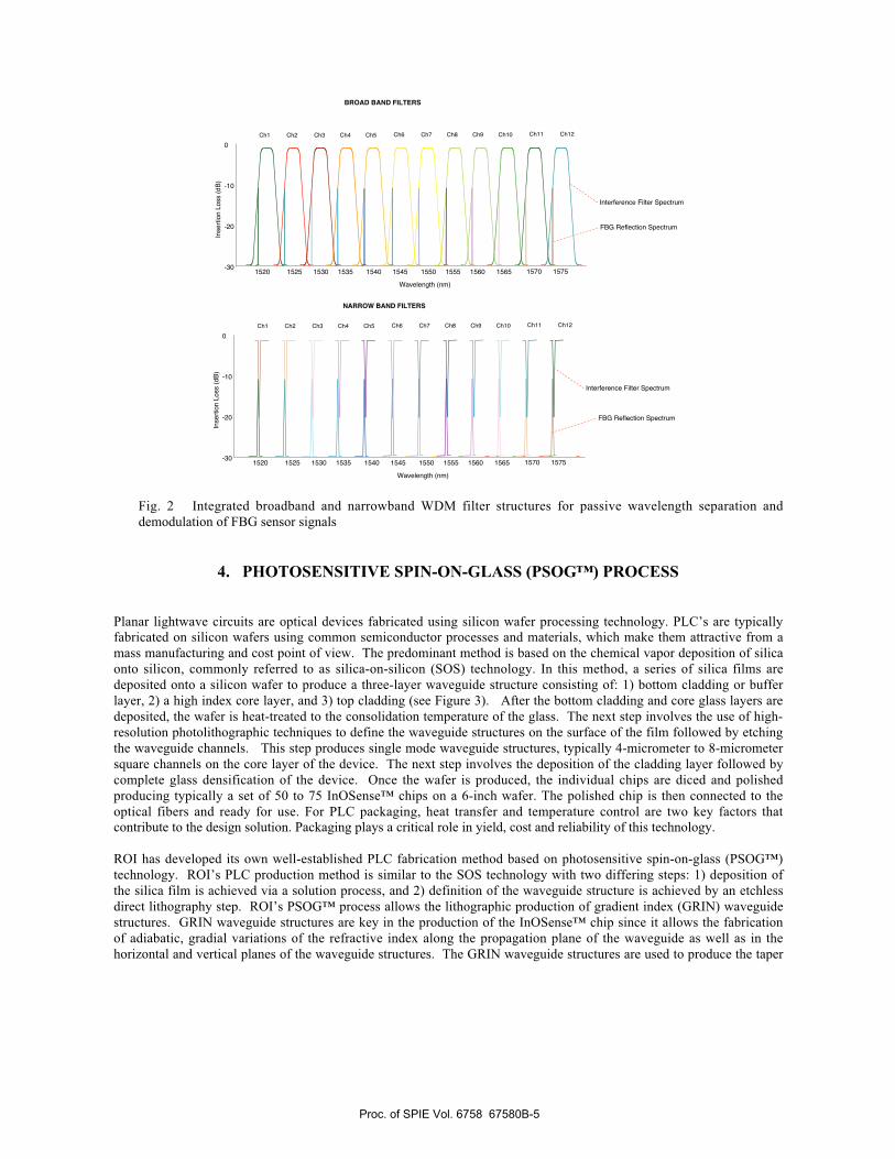
Two types of wavelength division multiplexing (WDM) waveguide architectures are used in the InOSense™ microchip
for the spectral separation of the individual wavelengths of each FBG sensors in the fiber sensor array. One type, used
with the low channel count (< 12-channels) FBG-Transceiver™ units, uses wavelength selective dispersive filter
structures, the other type, used with the high channel count (> 12 channels) FBG-Transceiver™ units, uses array
waveguide grating (AWG) architectures. The wavelength selective WDM structures allows the transmission of a
particular FBG wavelength (�1) while reflecting, or separating, all of the other (�2, �3, �n) FBG sensor wavelengths to the
respective detection channels. This process is repeated, wavelength specific, at each photodetector to achieve a
wavelength demultiplexing PLC structure. WDM filters are commonly used in long haul fiber optic telecommunication
networks to either mix (multiplex) or separate (demultiplex) large numbers of communication wavelengths. By carefully
selecting the spectral optical bandpass properties of the filter, the peak wavelength shift, environmentally induced,
optical signal from each of the FBG sensors is converted into a linear intensity variation, directly related to the physical
state (peak wavelength position) of the FBG sensor at the photodetector element, as shown in Figure 2. This principle
forms the basis of the FBG sensor demodulator in the InOSense™ microchip.
Proc. of SPIE Vol. 6758 67580B-4
0
-10
-20
-30
Wavelength (nm)
1520 1525 1530 1535 1540
FBG Reflection Spectrum
Interference Filter Spectrum
Ch1 Ch2 Ch3 Ch4 Ch5 Ch6 Ch7 Ch8 Ch9 Ch10 Ch11 Ch12
1545 1550 1555 1560 1565 1570 1575
BROAD BAND FILTERS
0
-10
-20
-30
Wavelength (nm)
1520 1525 1530 1535 1540
FBG Reflection Spectrum
Interference Filter Spectrum
Ch1 Ch2 Ch3 Ch4 Ch5 Ch6 Ch7 Ch8 Ch9 Ch10 Ch11 Ch12
1545 1550 1555 1560 1565 1570 1575
NARROW BAND FILTERS
Fig. 2 Integrated broadband and narrowband WDM filter structures for passive wavelength separation and
demodulation of FBG sensor signals
4. PHOTOSENSITIVE SPIN-ON-GLASS (PSOG™) PROCESS
Planar lightwave circuits are optical devices fabricated using silicon wafer processing technology. PLC’s are typically
fabricated on silicon wafers using common semiconductor processes and materials, which make them attractive from a
mass manufacturing and cost point of view. The predominant method is based on the chemical vapor deposition of silica
onto silicon, commonly referred to as silica-on-silicon (SOS) technology. In this method, a series of silica films are
deposited onto a silicon wafer to produce a three-layer waveguide structure consisting of: 1) bottom cladding or buffer
layer, 2) a high index core layer, and 3) top cladding (see Figure 3). After the bottom cladding and core glass layers are
deposited, the wafer is heat-treated to the consolidation temperature of the glass. The next step involves the use of high-
resolution photolithographic techniques to define the waveguide structures on the surface of the film followed by etching
the waveguide channels. This step produces single mode waveguide structures, typically 4-micrometer to 8-micrometer
square channels on the core layer of the device. The next step involves the deposition of the cladding layer followed by
complete glass densification of the device. Once the wafer is produced, the individual chips are diced and polished
producing typically a set of 50 to 75 InOSense™ chips on a 6-inch wafer. The polished chip is then connected to the
optical fibers and ready for use. For PLC packaging, heat transfer and temperature control are two key factors that
contribute to the design solution. Packaging plays a critical role in yield, cost and reliability of this technology.
ROI has developed its own well-established PLC fabrication method based on photosensitive spin-on-glass (PSOG™)
technology. ROI’s PLC production method is similar to the SOS technology with two differing steps: 1) deposition of
the silica film is achieved via a solution process, and 2) definition of the waveguide structure is achieved by an etchless
direct lithography step. ROI’s PSOG™ process allows the lithographic production of gradient index (GRIN) waveguide
structures. GRIN waveguide structures are key in the production of the InOSense™ chip since it allows the fabrication
of adiabatic, gradial variations of the refractive index along the propagation plane of the waveguide as well as in the
horizontal and vertical planes of the waveguide structures. The GRIN waveguide structures are used to produce the taper
Proc. of SPIE Vol. 6758 67580B-5
Mixing
Coating
Soft Bake
Lithography
I Hard Bake
CladdingCoreCladdingSilica Layer
Substrate
mode adapters used to enhance the mode coupling efficiency from the SLED source to the waveguide, and also to
produce taper structures used for the WDM wavelength separation and demodulation of the FBG sensor signals.
Fig. 3 PSOG™ Planar Lightwave Circuit Fabrication Process
ROI’s adiabatic mode coupling waveguide structures allow the complete control of the light confinement strength along
the light propagation axis of the waveguide structure. This is accomplished by gradually controlling the refractive index
of the PLC waveguide structure at any location of the three-dimensional space of the waveguide, as shown in Figure 4.
In ROI’s transverse-transfer mode coupling waveguide structures, the core and the surrounding vertical and horizontal
cladding material each have a refractive index profile that is gradually controlled in the direction of light propagation.
For these types of structures, it is possible to tailor the velocity of light propagating through the core of the waveguide
and the light confinement strength of the waveguide for any given cross section. Such waveguide structures can be used
for mode matching an input or output of a high �n optical device, such as the SLED die, to the low �n of the PLC
waveguide. They can also be used in the construction of reflective taper structures to maximize the coupling efficiency
of incoming light from the WDM filter to a tapered waveguide. Using this approach, complex adiabatic waveguide
structures can be produced to achieve close to 100 % efficiency of optical transfer power from an optical device to a
GRIN-PLC waveguide structure. These types of adiabatic structures are key to the design of the InOSense™ microchip
and to maximize the power budget efficiency of the chip.
nCoren
z
nCl
nClvnClh
nCore
Light PropagationnCoren
z
nClnClvnClh
nCore
Light Propagation
Fig. 4 GRIN adiabatic mode coupler waveguide structures
5. PRELIMINARY DEMONSTRATION OF OPERATING PRINCIPLE OF MINIATURE
FBG-TRANSCEIVER™ SYSTEM
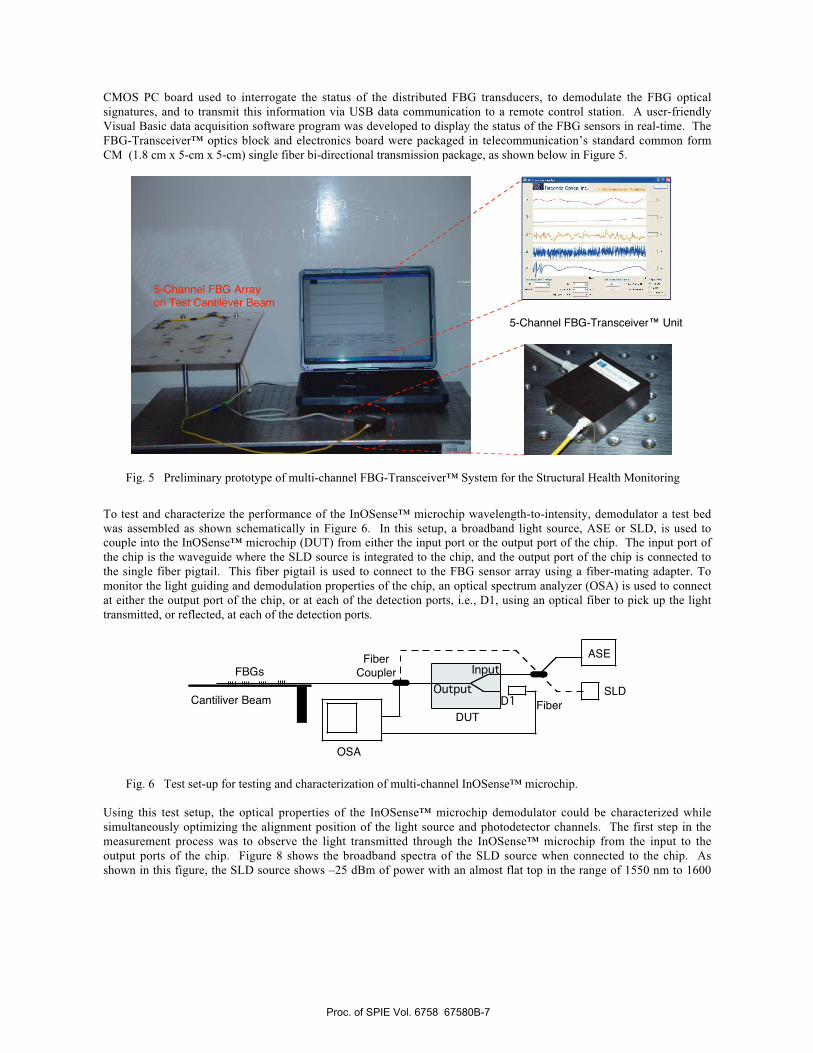
To demonstrate the operating principle of the miniature fiber Bragg grating sensor interrogator FBG-Transceiver™
technology, a proof-of-concept prototype unit was developed based on ROI’s proprietary multi-channel integrated optic
sensor (InOSense™) microchip technology. ROI designed and produced a state-of-the-art signal processing electronics
Proc. of SPIE Vol. 6758 67580B-6
C
- __j_s.. — —1=
a'
CMOS PC board used to interrogate the status of the distributed FBG transducers, to demodulate the FBG optical
signatures, and to transmit this information via USB data communication to a remote control station. A user-friendly
Visual Basic data acquisition software program was developed to display the status of the FBG sensors in real-time. The
FBG-Transceiver™ optics block and electronics board were packaged in telecommunication’s standard common form
CM (1.8 cm x 5-cm x 5-cm) single fiber bi-directional transmission package, as shown below in Figure 5.
5-Channel FBG-Transceiver™ Unit
5-Channel FBG Array on Test Cantilever Beam
Fig. 5 Preliminary prototype of multi-channel FBG-Transceiver™ System for the Structural Health Monitoring
To test and characterize the performance of the InOSense™ microchip wavelength-to-intensity, demodulator a test bed
was assembled as shown schematically in Figure 6. In this setup, a broadband light source, ASE or SLD, is used to
couple into the InOSense™ microchip (DUT) from either the input port or the output port of the chip. The input port of
the chip is the waveguide where the SLD source is integrated to the chip, and the output port of the chip is connected to
the single fiber pigtail. This fiber pigtail is used to connect to the FBG sensor array using a fiber-mating adapter. To
monitor the light guiding and demodulation properties of the chip, an optical spectrum analyzer (OSA) is used to connect
at either the output port of the chip, or at each of the detection ports, i.e., D1, using an optical fiber to pick up the light
transmitted, or reflected, at each of the detection ports.
OSA
ASE
SLDFiber
DUT
FiberCouplerFBGs Input
OutputD1Cantiliver Beam
Fig. 6 Test set-up for testing and characterization of multi-channel InOSense™ microchip.
Using this test setup, the optical properties of the InOSense™ microchip demodulator could be characterized while
simultaneously optimizing the alignment position of the light source and photodetector channels. The first step in the
measurement process was to observe the light transmitted through the InOSense™ microchip from the input to the
output ports of the chip. Figure 8 shows the broadband spectra of the SLD source when connected to the chip. As
shown in this figure, the SLD source shows –25 dBm of power with an almost flat top in the range of 1550 nm to 1600
Proc. of SPIE Vol. 6758 67580B-7
9—
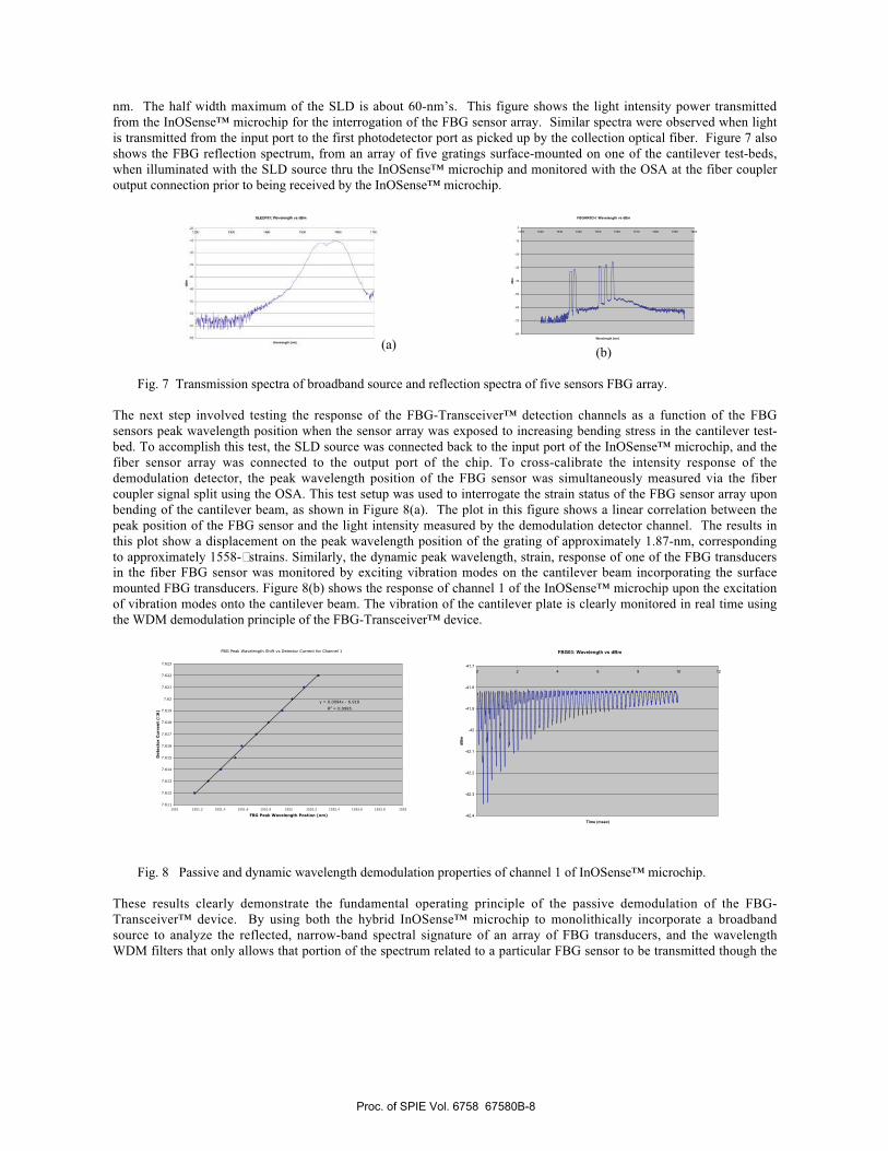
nm. The half width maximum of the SLD is about 60-nm’s. This figure shows the light intensity power transmitted
from the InOSense™ microchip for the interrogation of the FBG sensor array. Similar spectra were observed when light
is transmitted from the input port to the first photodetector port as picked up by the collection optical fiber. Figure 7 also
shows the FBG reflection spectrum, from an array of five gratings surface-mounted on one of the cantilever test-beds,
when illuminated with the SLD source thru the InOSense™ microchip and monitored with the OSA at the fiber coupler
output connection prior to being received by the InOSense™ microchip.
(a)
FBGAR5CH: Wavelength vs dBm
-80
-70
-60
-50
-40
-30
-20
-10
0
1510 1520 1530 1540 1550 1560 1570 1580 1590 1600
Wavelength [nm]
dB
m
(b)
Fig. 7 Transmission spectra of broadband source and reflection spectra of five sensors FBG array.
The next step involved testing the response of the FBG-Transceiver™ detection channels as a function of the FBG
sensors peak wavelength position when the sensor array was exposed to increasing bending stress in the cantilever test-
bed. To accomplish this test, the SLD source was connected back to the input port of the InOSense™ microchip, and the
fiber sensor array was connected to the output port of the chip. To cross-calibrate the intensity response of the
demodulation detector, the peak wavelength position of the FBG sensor was simultaneously measured via the fiber
coupler signal split using the OSA. This test setup was used to interrogate the strain status of the FBG sensor array upon
bending of the cantilever beam, as shown in Figure 8(a). The plot in this figure shows a linear correlation between the
peak position of the FBG sensor and the light intensity measured by the demodulation detector channel. The results in
this plot show a displacement on the peak wavelength position of the grating of approximately 1.87-nm, corresponding
to approximately 1558-�strains. Similarly, the dynamic peak wavelength, strain, response of one of the FBG transducers
in the fiber FBG sensor was monitored by exciting vibration modes on the cantilever beam incorporating the surface
mounted FBG transducers. Figure 8(b) shows the response of channel 1 of the InOSense™ microchip upon the excitation
of vibration modes onto the cantilever beam. The vibration of the cantilever plate is clearly monitored in real time using
the WDM demodulation principle of the FBG-Transceiver™ device.
FBG03: Wavelength vs dBm
-42.4
-42.3
-42.2
-42.1
-42
-41.9
-41.8
-41.7
0 2 4 6 8 10 12
Time (msec)
dB
m
Fig. 8 Passive and dynamic wavelength demodulation properties of channel 1 of InOSense™ microchip.
These results clearly demonstrate the fundamental operating principle of the passive demodulation of the FBG-
Transceiver™ device. By using both the hybrid InOSense™ microchip to monolithically incorporate a broadband
source to analyze the reflected, narrow-band spectral signature of an array of FBG transducers, and the wavelength
WDM filters that only allows that portion of the spectrum related to a particular FBG sensor to be transmitted though the
FBG Peak Wavelength Shift vs Detector Current for Channel 1
y = 0.0094x - 6.918
R2 = 0.9985
7.611
7.612
7.613
7.614
7.615
7.616
7.617
7.618
7.619
7.62
7.621
7.622
7.623
1551 1551.2 1551.4 1551.6 1551.8 1552 1552.2 1552.4 1552.6 1552.8 1553
FBG Peak Wavelength Postion (nm)
Dete
cto
r C
urren
t (�
A)
Proc. of SPIE Vol. 6758 67580B-8
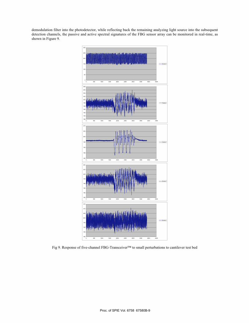
demodulation filter into the photodetector, while reflecting back the remaining analyzing light source into the subsequent
detection channels, the passive and active spectral signatures of the FBG sensor array can be monitored in real-time, as
shown in Figure 9.
0
50
100
150
200
250
300
0 500 1000 1500 2000 2500 3000 3500 4000 4500
Series1
188
190
192
194
196
198
200
202
204
206
208
0 500 1000 1500 2000 2500 3000 3500 4000 4500
Series1
180
185
190
195
200
205
210
0 500 1000 1500 2000 2500 3000 3500 4000 4500
Series1
190
192
194
196
198
200
202
204
0 500 1000 1500 2000 2500 3000 3500 4000 4500
Series1
180
185
190
195
200
205
210
215
0 500 1000 1500 2000 2500 3000 3500 4000 4500
Series1
Fig 9. Response of five-channel FBG-Transceiver™ to small perturbations to cantilever test bed
Proc. of SPIE Vol. 6758 67580B-9
6. SUMMARY
The results presented in this paper described preliminary work towards the development of a miniature fiber Bragg
grating sensor interrogator (FBG-Transceiver™) system based on multi-channel integrated optic sensor (InOSense™)
microchip technology for applications where size, weight, and consumption power are critical for operation. The
preliminary test results of the FBG-Transceiver™ device conclusively demonstrated the demodulation principle of the
hybrid InOSense™ microchip for the accurate measurement of the peak wavelength shift of the FBG transducers when
the sensors are exposed to passive and active events. The hybrid InOSense™ microchip technology enables the
integration of all of the functionalities, both passive and active, of conventional bench-top FBG sensor interrogators
systems, packaged in a miniaturized, low power operation, single fiber package suitable for the long-term structural
health monitoring in aerospace and automotive applications.
7. ACKNOWLEDGMENTS
Redondo Optics acknowledges the support of this work from the U.S. Navy under an SBIR contract No. N68335-06-C-
0206.
REFERENCES
1. Mendoza, E. A., Principal Investigator, “Miniaturization of an Optical Fiber Grating Sensor Interrogator,” Navy
Phase I SBIR Contract No. N68335-06-C-0049.
2. Buswell, J., “Lessons Learned from Health Monitoring of Rocket Motors,” 41st
AIAA/ASME/SAE/ASEE Joint
Propulsion Conference and Exhibit, AIAA 2005-4558, 10-13 July 2005, Tucson, AZ
3. Mendoza, E. A., Fiber Bragg Grating Sensor Interrogator and Manufacture Thereof,” US Patent Application No.
11/443,618, 2006.
Proc. of SPIE Vol. 6758 67580B-10
Related Documents


![paper w mod · detection of composite materials (e.g., Ref. [12]). Webb et al. [13,14] applied a dynamic full-spectrum FBG interrogator to a single FBG sensor embedded in the adhesive](https://static.cupdf.com/doc/110x72/5f05c3477e708231d414950e/paper-w-detection-of-composite-materials-eg-ref-12-webb-et-al-1314.jpg)
![Microindentation Sensor System Based ... - Fiber Bragg Grating · characterizations with high spatial resolution. An integrated fiber Bragg grating (FBG) acts as a force sensor [25].](https://static.cupdf.com/doc/110x72/5eb728e156b9257755281a1a/microindentation-sensor-system-based-fiber-bragg-grating-characterizations.jpg)