Materials Chemistry and Physics 71 (2001) 255–271 Microstructure evolution in Sn–Bi and Sn–Bi–Cu solder joints under thermal aging Hui-Wei Miao, Jenq-Gong Duh ∗ Department of Materials Science and Engineering, National Tsing-Hua University, 101, Kuang Fu Road, Sec. 2, Hsin-Chu 300, Taiwan Received 15 June 2000; received in revised form 13 January 2001; accepted 18 January 2001 Abstract Binary eutectic Sn–Bi and ternary Sn–Bi–Cu alloys were fabricated and soldered to conductor metallized substrates to study the interfacial morphology and microstructural evolution of the joints under thermal aging. Different types of intermetallic compound (IMC), such as Cu 6 Sn 5 , (Cu, Ni) 6 Sn 5 and Ag 3 Sn, are observed among various metallized substrates including Cu/FR4, Ni/Cu/FR4, Cu/Al 2 O 3 and Pt–Ag/Al 2 O 3 . Three major effects of aging on the microstructure of the solder joints are observed. First, the coarsening rate of the Bi-rich phase in the solder joint under thermal aging at 120 ◦ C is reduced by adding 1 wt.% Cu to the 42Sn–58Bi solder. Second, the Ag 3 Sn IMC forms planar layer at the solder/PtAg interface, while the Cu 6 Sn 5 intermetallic grows as scallop-like grains into the solder at the Cu/solder interface. Third, the growth of Ag 3 Sn intermetallic in the SnBi–1Cu/PtAg solder joint is slower than that in the 42Sn–58Bi/PtAg joint after thermal aging at 120 ◦ C. © 2001 Elsevier Science B.V. All rights reserved. Keywords: Solder; Intermetallic compound; Thermal aging; Interfacial morphology; Microstructure 1. Introduction Solder joint is an essential part of electronic devices since it plays a key role not only as an electrical connection but also as a mechanical bond [1,2]. Currently, solder joints with higher reliability is demanding because the trend in elec- tronic package is to make products smaller and faster. With appropriate joint design, the use of solder alloys with ex- cellent properties, and the employment of a better process, reliable joints are obtained. The eutectic SnPb alloys are the most widely used solder material today [1,3–6]. However, there are environmental concerns about the toxicity of Pb in the SnPb solder alloys [3–5,7–12]. Thus, it is a research focus in recent years to develop alternative Pb-free solders. During soldering, a considerable strain is produced in the board [13]. Fortunately, the residual strain may be reduced by using a lower melting point solder. The eutectic SnBi alloy is a possible Pb-free solder for low temperature sol- dering due to its low melting temperature. When devices to be soldered are subject to thermal damage, low tempera- ture soldering is necessary [3,14]. Low temperature solder- ing can also reduce the damage of thermal cycling caused by thermal expansion mismatch among various materials in an electronic package [14]. ∗ Corresponding author. Tel./fax: +886-3-571-2686. E-mail address: [email protected] (J.-G. Duh). The tensile strength of the eutectic SnBi solder is higher than that of the eutectic SnPb solder [1,13]. In addition, the 42Sn–58Bi solder has a better creep resistance than the eu- tectic Sn–Pb solder [1,7,15]. However, the 42Sn–58Bi solder alloy exhibits noticeable microstructure coarsening during thermal aging [7,8,10,12,15]. The microstructure instability at elevated temperature can be suppressed by incorporating fine dispersoid particles into the eutectic SnBi solder alloys. The solder microstructure and the growth of intermetallic compound (IMC) at the solder/metallization interface sig- nificantly influence solder joint reliability. The IMC can be a source of mechanical weakness in soldered joints due to its brittle cracking, or delimitation. With the increase of ag- ing time, the fracture occurs at a different position from that of as-soldered joints [16,17]. Characterizing the formation and growth of IMC in the solder joint is thus critical and models were employed to demonstrate the interfacial phase transformation using an effective approach by Lee and Duh [18]. Interfacial morphology and phase analysis were also revealed in Sn–Cu solder joints [19,20]. Recently, Wei and Duh [21] reported the effect of thermal aging on Sn–Ag sol- der joints. Thermal cycling test in Sn–Bi and Sn–Bi–Cu sol- der joints was also investigated [22]. This study is aimed to evaluate the effect of the thermal aging on the microstruc- tural evolution and IMC growth for the Sn–Bi solder on var- ious metallized substrate. Morphology variation and phase transformation of the solder joint will be investigated. The 0254-0584/01/$ – see front matter © 2001 Elsevier Science B.V. All rights reserved. PII:S0254-0584(01)00298-X

Welcome message from author
This document is posted to help you gain knowledge. Please leave a comment to let me know what you think about it! Share it to your friends and learn new things together.
Transcript
Materials Chemistry and Physics 71 (2001) 255–271
Microstructure evolution in Sn–Bi and Sn–Bi–Cusolder joints under thermal aging
Hui-Wei Miao, Jenq-Gong Duh∗Department of Materials Science and Engineering, National Tsing-Hua University, 101, Kuang Fu Road, Sec. 2, Hsin-Chu 300, Taiwan
Received 15 June 2000; received in revised form 13 January 2001; accepted 18 January 2001
Abstract
Binary eutectic Sn–Bi and ternary Sn–Bi–Cu alloys were fabricated and soldered to conductor metallized substrates to study theinterfacial morphology and microstructural evolution of the joints under thermal aging. Different types of intermetallic compound (IMC),such as Cu6Sn5, (Cu, Ni)6Sn5 and Ag3Sn, are observed among various metallized substrates including Cu/FR4, Ni/Cu/FR4, Cu/Al2O3 andPt–Ag/Al2O3. Three major effects of aging on the microstructure of the solder joints are observed. First, the coarsening rate of the Bi-richphase in the solder joint under thermal aging at 120◦C is reduced by adding 1 wt.% Cu to the 42Sn–58Bi solder. Second, the Ag3Sn IMCforms planar layer at the solder/PtAg interface, while the Cu6Sn5 intermetallic grows as scallop-like grains into the solder at the Cu/solderinterface. Third, the growth of Ag3Sn intermetallic in the SnBi–1Cu/PtAg solder joint is slower than that in the 42Sn–58Bi/PtAg joint afterthermal aging at 120◦C. © 2001 Elsevier Science B.V. All rights reserved.
Keywords: Solder; Intermetallic compound; Thermal aging; Interfacial morphology; Microstructure
1. Introduction
Solder joint is an essential part of electronic devices sinceit plays a key role not only as an electrical connection butalso as a mechanical bond [1,2]. Currently, solder joints withhigher reliability is demanding because the trend in elec-tronic package is to make products smaller and faster. Withappropriate joint design, the use of solder alloys with ex-cellent properties, and the employment of a better process,reliable joints are obtained. The eutectic SnPb alloys are themost widely used solder material today [1,3–6]. However,there are environmental concerns about the toxicity of Pbin the SnPb solder alloys [3–5,7–12]. Thus, it is a researchfocus in recent years to develop alternative Pb-free solders.During soldering, a considerable strain is produced in theboard [13]. Fortunately, the residual strain may be reducedby using a lower melting point solder. The eutectic SnBialloy is a possible Pb-free solder for low temperature sol-dering due to its low melting temperature. When devicesto be soldered are subject to thermal damage, low tempera-ture soldering is necessary [3,14]. Low temperature solder-ing can also reduce the damage of thermal cycling causedby thermal expansion mismatch among various materials inan electronic package [14].
∗ Corresponding author. Tel./fax: +886-3-571-2686.E-mail address: [email protected] (J.-G. Duh).
The tensile strength of the eutectic SnBi solder is higherthan that of the eutectic SnPb solder [1,13]. In addition, the42Sn–58Bi solder has a better creep resistance than the eu-tectic Sn–Pb solder [1,7,15]. However, the 42Sn–58Bi solderalloy exhibits noticeable microstructure coarsening duringthermal aging [7,8,10,12,15]. The microstructure instabilityat elevated temperature can be suppressed by incorporatingfine dispersoid particles into the eutectic SnBi solder alloys.
The solder microstructure and the growth of intermetalliccompound (IMC) at the solder/metallization interface sig-nificantly influence solder joint reliability. The IMC can bea source of mechanical weakness in soldered joints due toits brittle cracking, or delimitation. With the increase of ag-ing time, the fracture occurs at a different position from thatof as-soldered joints [16,17]. Characterizing the formationand growth of IMC in the solder joint is thus critical andmodels were employed to demonstrate the interfacial phasetransformation using an effective approach by Lee and Duh[18]. Interfacial morphology and phase analysis were alsorevealed in Sn–Cu solder joints [19,20]. Recently, Wei andDuh [21] reported the effect of thermal aging on Sn–Ag sol-der joints. Thermal cycling test in Sn–Bi and Sn–Bi–Cu sol-der joints was also investigated [22]. This study is aimed toevaluate the effect of the thermal aging on the microstruc-tural evolution and IMC growth for the Sn–Bi solder on var-ious metallized substrate. Morphology variation and phasetransformation of the solder joint will be investigated. The
0254-0584/01/$ – see front matter © 2001 Elsevier Science B.V. All rights reserved.PII: S0 2 5 4 -0 5 84 (01 )00298 -X
256 H.-W. Miao, J.-G. Duh / Materials Chemistry and Physics 71 (2001) 255–271
Fig. 1. Schematical diagram of the soldered coupons.
influence of Cu addition to the binary Sn–Bi solder is alsodiscussed.
2. Experimental procedures
2.1. Fabrication of solder alloys
The eutectic Sn–Bi and ternary SnBi–1 wt.% Cu solderalloys were fabricated from raw materials including pure
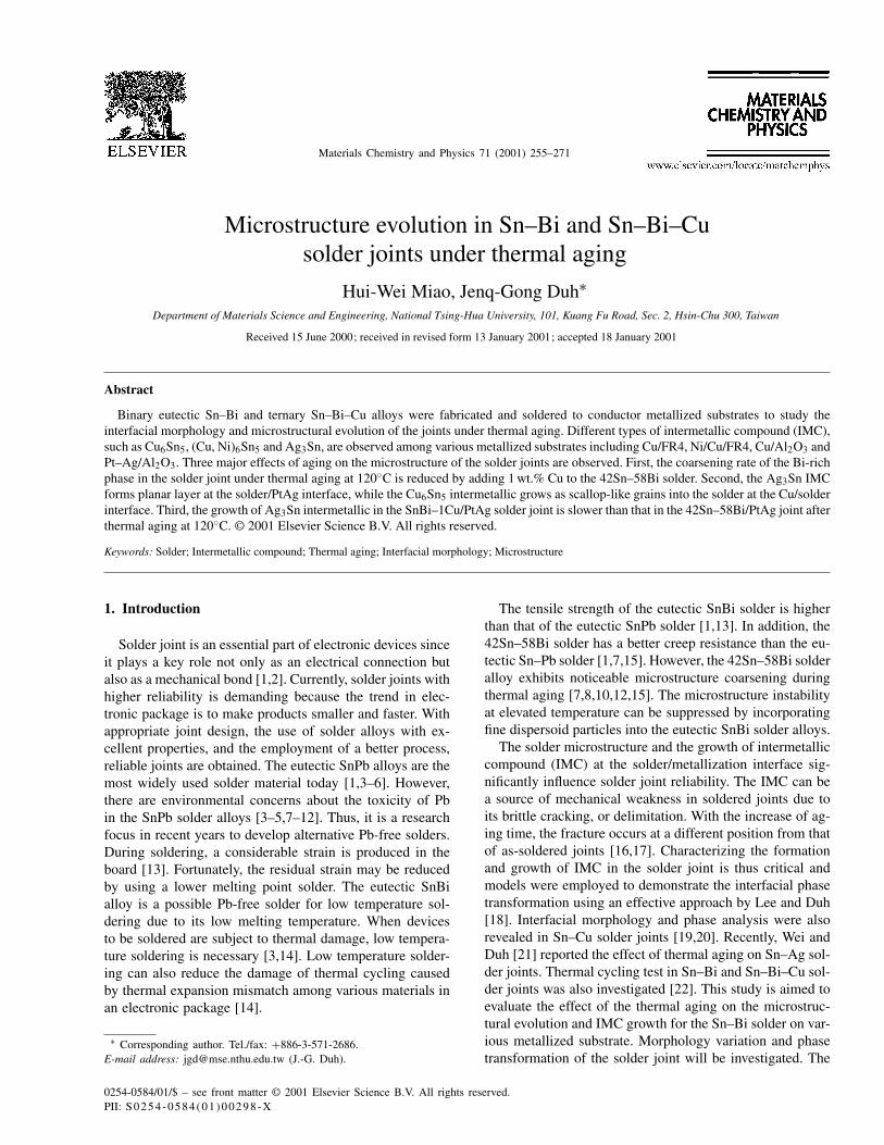
Fig. 2. Micrographs of 42Sn–58Bi/Cu/FR4 solder joint before aging: (a) SEI; (b) Sn mapping; (c) Bi mapping; (d) Cu mapping.
tin, bismuth and copper by vacuum melting with continuousrotation for the purpose of homogenization.
The composition of the as-fabricated binary Sn–Bi sol-der as measured by electron probe microanalyzer (EPMA,JXA-8800M, JEOL, Japan) is 42.4 wt.% Sn–57.6 wt.%Bi, which is fairly close to the eutectic 42Sn–58Bi in thephase diagram. As to the ternary solder, the measuredcomposition is 43.2 wt.% Sn–55.8 wt.% Bi–1.0 wt.% Cu.There is a little deviation from the nominal 41.6 wt.%Sn–57.4 wt.% Bi–1 wt.% Cu possibly due to Bi loss in themelting.
Metallized ceramic substrates of Cu/Al2O3 and PtAg/Al2O3 were dipped into a batch of molten as-fabricatedsolders at 200◦C, and followed by reflowing. Thus, theas-fabricated solder/conductor/Al2O3 joint was derived. Onthe other hand, a commercial eutectic 42Sn–58Bi solderpaste with 88 wt.% metal and 12 wt.% RMA flux was appliedto the FR4 substrate metallized with either Cu or Au/Ni/Cu.An 1206 LCCC capacitor was soldered on Cu metallizedFR4, while an 8-pin SMT was soldered on the Au/Ni/Cumetallized FR4. Schematical diagrams of solder joints areshown in Fig. 1.
2.2. Thermal aging
Solder joints were aged at 100 or 120◦C for various timeto evaluate the morphology and IMC growth near the in-terface of the joints. Soldered FR4 substrates were agedat 100◦C, while soldered Al2O3 substrates were aged at120◦C.
H.-W. Miao, J.-G. Duh / Materials Chemistry and Physics 71 (2001) 255–271 257
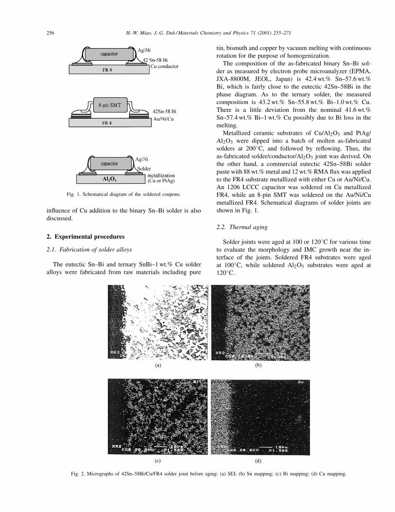
Fig. 3. Micrographs of 42Sn–58Bi/Cu/FR4 solder joint after 49 days aging at 100◦C: (a) SEI; (b) Sn mapping; (c) Bi mapping; (d) Cu mapping.
2.3. Microstructural characterization
The phase and crystal structure of the solder joints wereidentified with an X-ray diffractometer with a wavelength ofCu K� (� = 1.5406 Å). The interfacial morphology of thejoints was analyzed with a scanning electron microprobe.The compositions and X-ray mapping were evaluated withan EPMA.
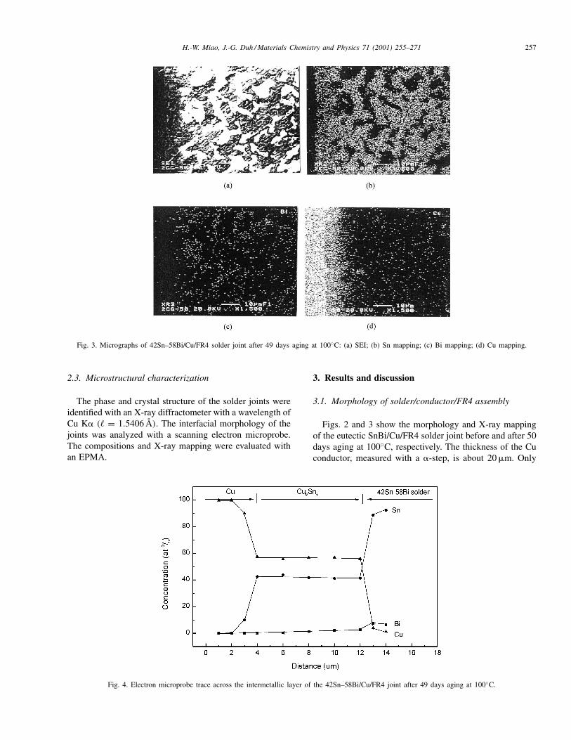
Fig. 4. Electron microprobe trace across the intermetallic layer of the 42Sn–58Bi/Cu/FR4 joint after 49 days aging at 100◦C.
3. Results and discussion
3.1. Morphology of solder/conductor/FR4 assembly
Figs. 2 and 3 show the morphology and X-ray mappingof the eutectic SnBi/Cu/FR4 solder joint before and after 50days aging at 100◦C, respectively. The thickness of the Cuconductor, measured with a �-step, is about 20 �m. Only
258 H.-W. Miao, J.-G. Duh / Materials Chemistry and Physics 71 (2001) 255–271
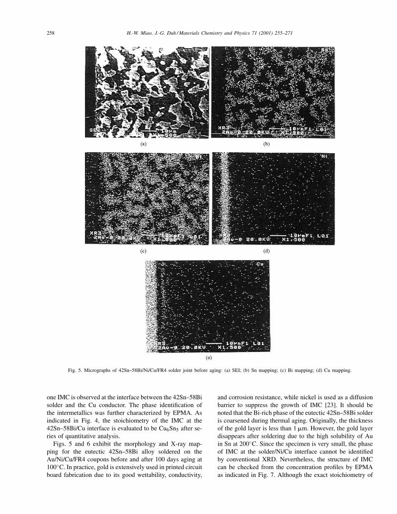
Fig. 5. Micrographs of 42Sn–58Bi/Ni/Cu/FR4 solder joint before aging: (a) SEI; (b) Sn mapping; (c) Bi mapping; (d) Cu mapping.
one IMC is observed at the interface between the 42Sn–58Bisolder and the Cu conductor. The phase identification ofthe intermetallics was further characterized by EPMA. Asindicated in Fig. 4, the stoichiometry of the IMC at the42Sn–58Bi/Cu interface is evaluated to be Cu6Sn5 after se-ries of quantitative analysis.
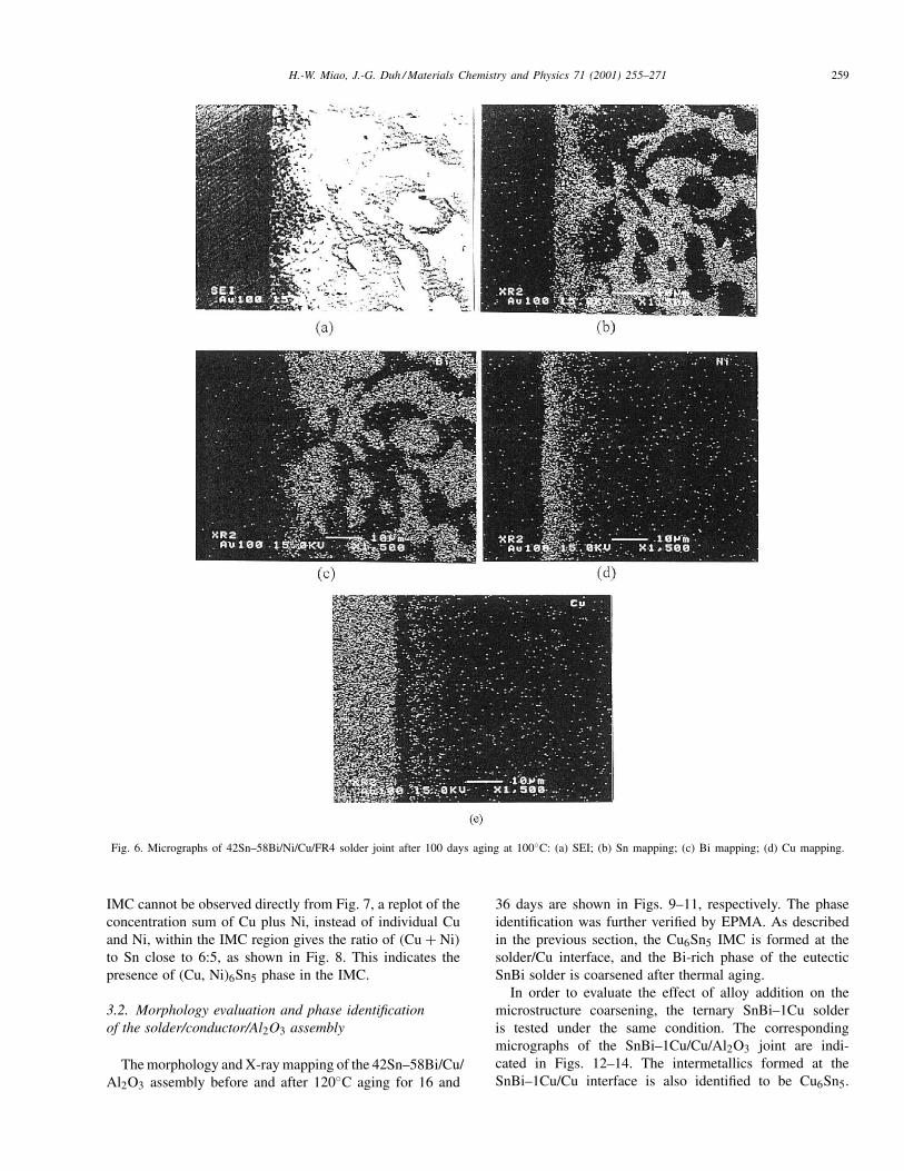
Figs. 5 and 6 exhibit the morphology and X-ray map-ping for the eutectic 42Sn–58Bi alloy soldered on theAu/Ni/Cu/FR4 coupons before and after 100 days aging at100◦C. In practice, gold is extensively used in printed circuitboard fabrication due to its good wettability, conductivity,
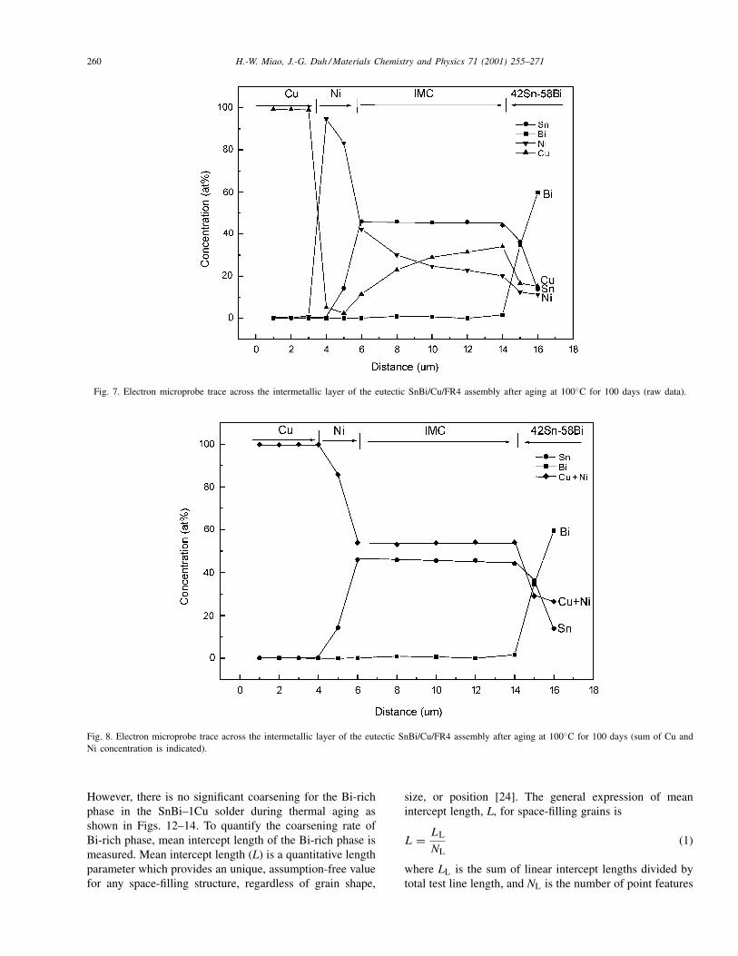
and corrosion resistance, while nickel is used as a diffusionbarrier to suppress the growth of IMC [23]. It should benoted that the Bi-rich phase of the eutectic 42Sn–58Bi solderis coarsened during thermal aging. Originally, the thicknessof the gold layer is less than 1 �m. However, the gold layerdisappears after soldering due to the high solubility of Auin Sn at 200◦C. Since the specimen is very small, the phaseof IMC at the solder/Ni/Cu interface cannot be identifiedby conventional XRD. Nevertheless, the structure of IMCcan be checked from the concentration profiles by EPMAas indicated in Fig. 7. Although the exact stoichiometry of
H.-W. Miao, J.-G. Duh / Materials Chemistry and Physics 71 (2001) 255–271 259
Fig. 6. Micrographs of 42Sn–58Bi/Ni/Cu/FR4 solder joint after 100 days aging at 100◦C: (a) SEI; (b) Sn mapping; (c) Bi mapping; (d) Cu mapping.
IMC cannot be observed directly from Fig. 7, a replot of theconcentration sum of Cu plus Ni, instead of individual Cuand Ni, within the IMC region gives the ratio of (Cu + Ni)to Sn close to 6:5, as shown in Fig. 8. This indicates thepresence of (Cu, Ni)6Sn5 phase in the IMC.
3.2. Morphology evaluation and phase identificationof the solder/conductor/Al2O3 assembly
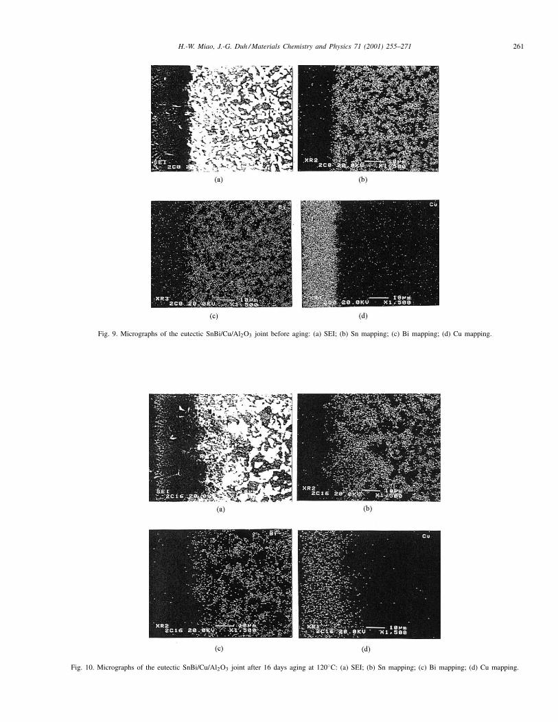
The morphology and X-ray mapping of the 42Sn–58Bi/Cu/Al2O3 assembly before and after 120◦C aging for 16 and
36 days are shown in Figs. 9–11, respectively. The phaseidentification was further verified by EPMA. As describedin the previous section, the Cu6Sn5 IMC is formed at thesolder/Cu interface, and the Bi-rich phase of the eutecticSnBi solder is coarsened after thermal aging.
In order to evaluate the effect of alloy addition on themicrostructure coarsening, the ternary SnBi–1Cu solderis tested under the same condition. The correspondingmicrographs of the SnBi–1Cu/Cu/Al2O3 joint are indi-cated in Figs. 12–14. The intermetallics formed at theSnBi–1Cu/Cu interface is also identified to be Cu6Sn5.
260 H.-W. Miao, J.-G. Duh / Materials Chemistry and Physics 71 (2001) 255–271
Fig. 7. Electron microprobe trace across the intermetallic layer of the eutectic SnBi/Cu/FR4 assembly after aging at 100◦C for 100 days (raw data).
Fig. 8. Electron microprobe trace across the intermetallic layer of the eutectic SnBi/Cu/FR4 assembly after aging at 100◦C for 100 days (sum of Cu andNi concentration is indicated).
However, there is no significant coarsening for the Bi-richphase in the SnBi–1Cu solder during thermal aging asshown in Figs. 12–14. To quantify the coarsening rate ofBi-rich phase, mean intercept length of the Bi-rich phase ismeasured. Mean intercept length (L) is a quantitative lengthparameter which provides an unique, assumption-free valuefor any space-filling structure, regardless of grain shape,
size, or position [24]. The general expression of meanintercept length, L, for space-filling grains is
L = LL
NL(1)
where LL is the sum of linear intercept lengths divided bytotal test line length, and NL is the number of point features
H.-W. Miao, J.-G. Duh / Materials Chemistry and Physics 71 (2001) 255–271 261
Fig. 9. Micrographs of the eutectic SnBi/Cu/Al2O3 joint before aging: (a) SEI; (b) Sn mapping; (c) Bi mapping; (d) Cu mapping.
Fig. 10. Micrographs of the eutectic SnBi/Cu/Al2O3 joint after 16 days aging at 120◦C: (a) SEI; (b) Sn mapping; (c) Bi mapping; (d) Cu mapping.
262 H.-W. Miao, J.-G. Duh / Materials Chemistry and Physics 71 (2001) 255–271
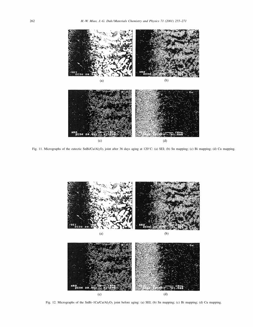
Fig. 11. Micrographs of the eutectic SnBi/Cu/Al2O3 joint after 36 days aging at 120◦C: (a) SEI; (b) Sn mapping; (c) Bi mapping; (d) Cu mapping.
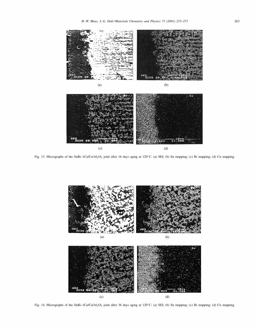
Fig. 12. Micrographs of the SnBi–1Cu/Cu/Al2O3 joint before aging: (a) SEI; (b) Sn mapping; (c) Bi mapping; (d) Cu mapping.
H.-W. Miao, J.-G. Duh / Materials Chemistry and Physics 71 (2001) 255–271 263
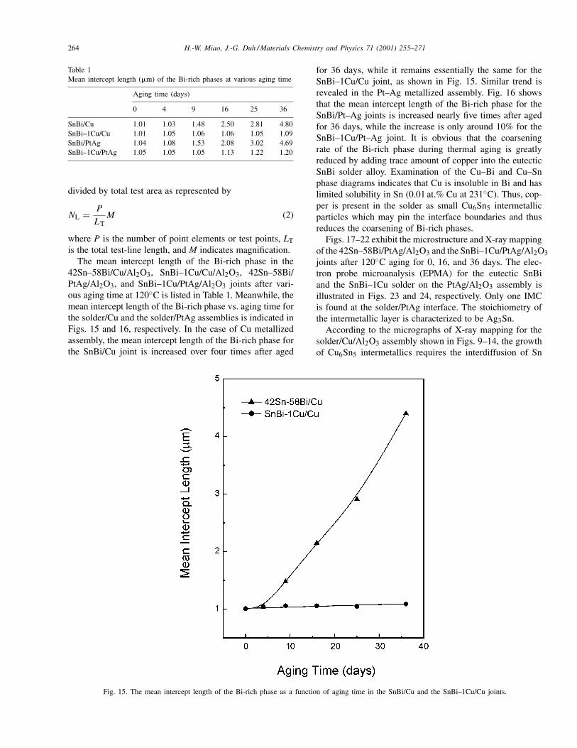
Fig. 13. Micrographs of the SnBi–1Cu/Cu/Al2O3 joint after 16 days aging at 120◦C: (a) SEI; (b) Sn mapping; (c) Bi mapping; (d) Cu mapping.
Fig. 14. Micrographs of the SnBi–1Cu/Cu/Al2O3 joint after 36 days aging at 120◦C: (a) SEI; (b) Sn mapping; (c) Bi mapping; (d) Cu mapping.
264 H.-W. Miao, J.-G. Duh / Materials Chemistry and Physics 71 (2001) 255–271
Table 1Mean intercept length (�m) of the Bi-rich phases at various aging time
Aging time (days)
0 4 9 16 25 36
SnBi/Cu 1.01 1.03 1.48 2.50 2.81 4.80SnBi–1Cu/Cu 1.01 1.05 1.06 1.06 1.05 1.09SnBi/PtAg 1.04 1.08 1.53 2.08 3.02 4.69SnBi–1Cu/PtAg 1.05 1.05 1.05 1.13 1.22 1.20
divided by total test area as represented by
NL = P
LTM (2)
where P is the number of point elements or test points, LTis the total test-line length, and M indicates magnification.
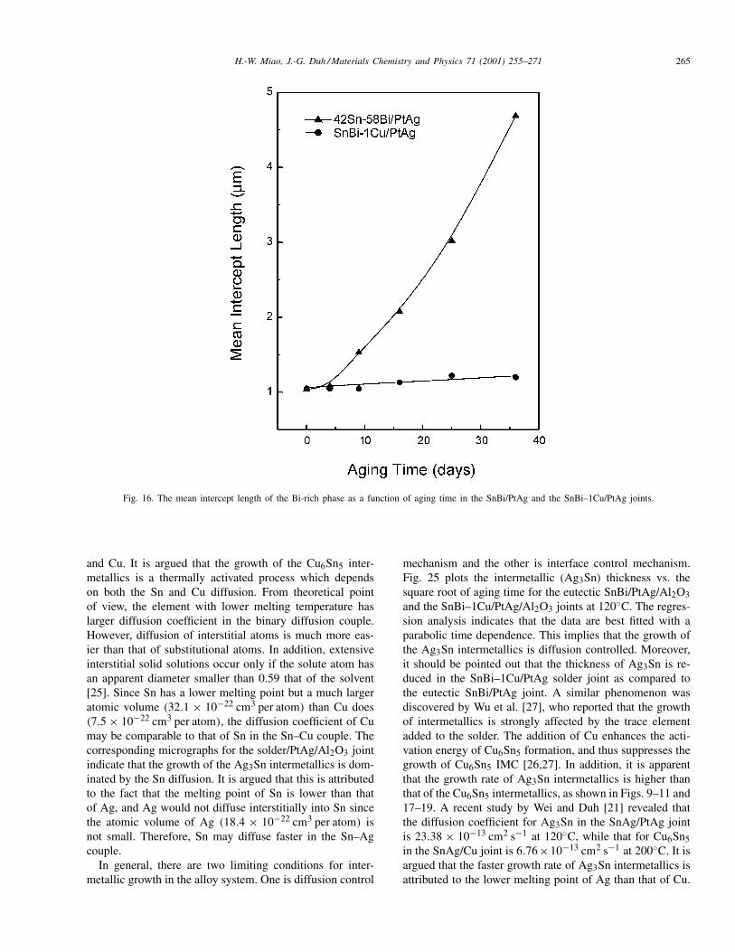
The mean intercept length of the Bi-rich phase in the42Sn–58Bi/Cu/Al2O3, SnBi–1Cu/Cu/Al2O3, 42Sn–58Bi/PtAg/Al2O3, and SnBi–1Cu/PtAg/Al2O3 joints after vari-ous aging time at 120◦C is listed in Table 1. Meanwhile, themean intercept length of the Bi-rich phase vs. aging time forthe solder/Cu and the solder/PtAg assemblies is indicated inFigs. 15 and 16, respectively. In the case of Cu metallizedassembly, the mean intercept length of the Bi-rich phase forthe SnBi/Cu joint is increased over four times after aged
Fig. 15. The mean intercept length of the Bi-rich phase as a function of aging time in the SnBi/Cu and the SnBi–1Cu/Cu joints.
for 36 days, while it remains essentially the same for theSnBi–1Cu/Cu joint, as shown in Fig. 15. Similar trend isrevealed in the Pt–Ag metallized assembly. Fig. 16 showsthat the mean intercept length of the Bi-rich phase for theSnBi/Pt–Ag joints is increased nearly five times after agedfor 36 days, while the increase is only around 10% for theSnBi–1Cu/Pt–Ag joint. It is obvious that the coarseningrate of the Bi-rich phase during thermal aging is greatlyreduced by adding trace amount of copper into the eutecticSnBi solder alloy. Examination of the Cu–Bi and Cu–Snphase diagrams indicates that Cu is insoluble in Bi and haslimited solubility in Sn (0.01 at.% Cu at 231◦C). Thus, cop-per is present in the solder as small Cu6Sn5 intermetallicparticles which may pin the interface boundaries and thusreduces the coarsening of Bi-rich phases.
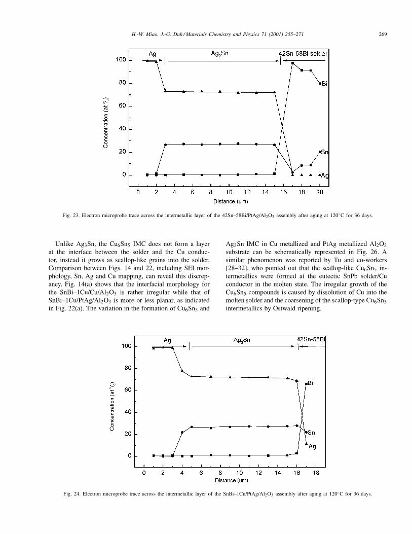
Figs. 17–22 exhibit the microstructure and X-ray mappingof the 42Sn–58Bi/PtAg/Al2O3 and the SnBi–1Cu/PtAg/Al2O3joints after 120◦C aging for 0, 16, and 36 days. The elec-tron probe microanalysis (EPMA) for the eutectic SnBiand the SnBi–1Cu solder on the PtAg/Al2O3 assembly isillustrated in Figs. 23 and 24, respectively. Only one IMCis found at the solder/PtAg interface. The stoichiometry ofthe intermetallic layer is characterized to be Ag3Sn.
According to the micrographs of X-ray mapping for thesolder/Cu/Al2O3 assembly shown in Figs. 9–14, the growthof Cu6Sn5 intermetallics requires the interdiffusion of Sn
H.-W. Miao, J.-G. Duh / Materials Chemistry and Physics 71 (2001) 255–271 265
Fig. 16. The mean intercept length of the Bi-rich phase as a function of aging time in the SnBi/PtAg and the SnBi–1Cu/PtAg joints.
and Cu. It is argued that the growth of the Cu6Sn5 inter-metallics is a thermally activated process which dependson both the Sn and Cu diffusion. From theoretical pointof view, the element with lower melting temperature haslarger diffusion coefficient in the binary diffusion couple.However, diffusion of interstitial atoms is much more eas-ier than that of substitutional atoms. In addition, extensiveinterstitial solid solutions occur only if the solute atom hasan apparent diameter smaller than 0.59 that of the solvent[25]. Since Sn has a lower melting point but a much largeratomic volume (32.1 × 10⁻²² cm3 per atom) than Cu does(7.5 × 10⁻²² cm3 per atom), the diffusion coefficient of Cumay be comparable to that of Sn in the Sn–Cu couple. Thecorresponding micrographs for the solder/PtAg/Al2O3 jointindicate that the growth of the Ag3Sn intermetallics is dom-inated by the Sn diffusion. It is argued that this is attributedto the fact that the melting point of Sn is lower than thatof Ag, and Ag would not diffuse interstitially into Sn sincethe atomic volume of Ag (18.4 × 10⁻²² cm3 per atom) isnot small. Therefore, Sn may diffuse faster in the Sn–Agcouple.
In general, there are two limiting conditions for inter-metallic growth in the alloy system. One is diffusion control
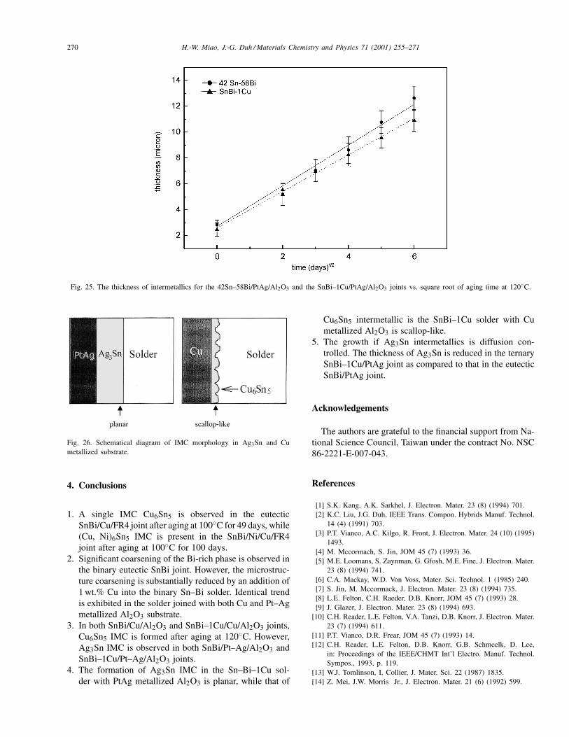
mechanism and the other is interface control mechanism.Fig. 25 plots the intermetallic (Ag3Sn) thickness vs. thesquare root of aging time for the eutectic SnBi/PtAg/Al2O3and the SnBi–1Cu/PtAg/Al2O3 joints at 120◦C. The regres-sion analysis indicates that the data are best fitted with aparabolic time dependence. This implies that the growth ofthe Ag3Sn intermetallics is diffusion controlled. Moreover,it should be pointed out that the thickness of Ag3Sn is re-duced in the SnBi–1Cu/PtAg solder joint as compared tothe eutectic SnBi/PtAg joint. A similar phenomenon wasdiscovered by Wu et al. [27], who reported that the growthof intermetallics is strongly affected by the trace elementadded to the solder. The addition of Cu enhances the acti-vation energy of Cu6Sn5 formation, and thus suppresses thegrowth of Cu6Sn5 IMC [26,27]. In addition, it is apparentthat the growth rate of Ag3Sn intermetallics is higher thanthat of the Cu6Sn5 intermetallics, as shown in Figs. 9–11 and17–19. A recent study by Wei and Duh [21] revealed thatthe diffusion coefficient for Ag3Sn in the SnAg/PtAg jointis 23.38 × 10⁻¹³ cm2 s−1 at 120◦C, while that for Cu6Sn5in the SnAg/Cu joint is 6.76×10⁻¹³ cm2 s−1 at 200◦C. It isargued that the faster growth rate of Ag3Sn intermetallics isattributed to the lower melting point of Ag than that of Cu.
266 H.-W. Miao, J.-G. Duh / Materials Chemistry and Physics 71 (2001) 255–271
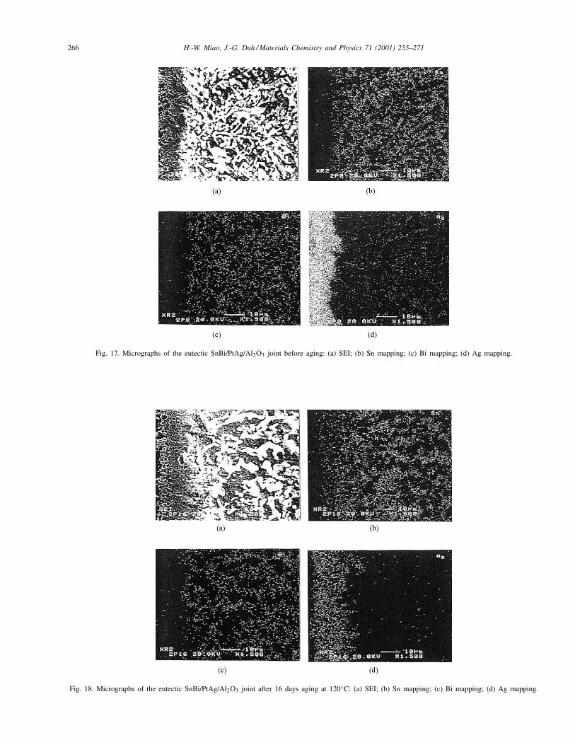
Fig. 17. Micrographs of the eutectic SnBi/PtAg/Al2O3 joint before aging: (a) SEI; (b) Sn mapping; (c) Bi mapping; (d) Ag mapping.
Fig. 18. Micrographs of the eutectic SnBi/PtAg/Al2O3 joint after 16 days aging at 120◦C: (a) SEI; (b) Sn mapping; (c) Bi mapping; (d) Ag mapping.
H.-W. Miao, J.-G. Duh / Materials Chemistry and Physics 71 (2001) 255–271 267
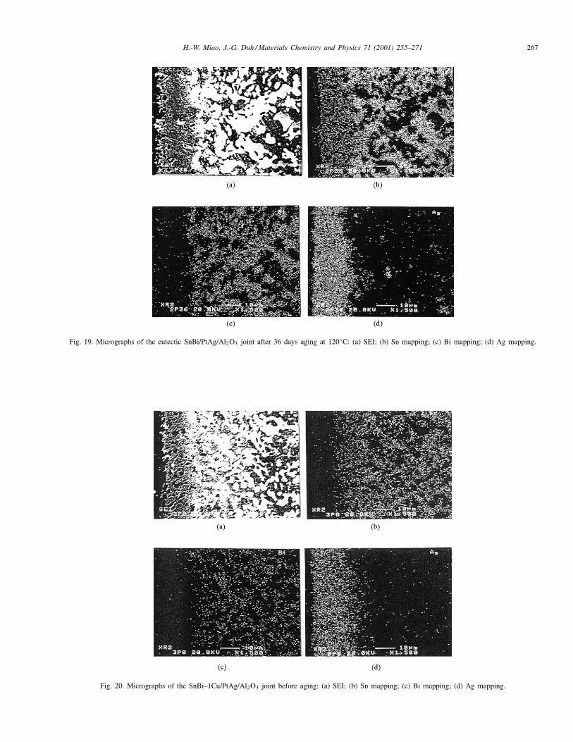
Fig. 19. Micrographs of the eutectic SnBi/PtAg/Al2O3 joint after 36 days aging at 120◦C: (a) SEI; (b) Sn mapping; (c) Bi mapping; (d) Ag mapping.
Fig. 20. Micrographs of the SnBi–1Cu/PtAg/Al2O3 joint before aging: (a) SEI; (b) Sn mapping; (c) Bi mapping; (d) Ag mapping.
268 H.-W. Miao, J.-G. Duh / Materials Chemistry and Physics 71 (2001) 255–271
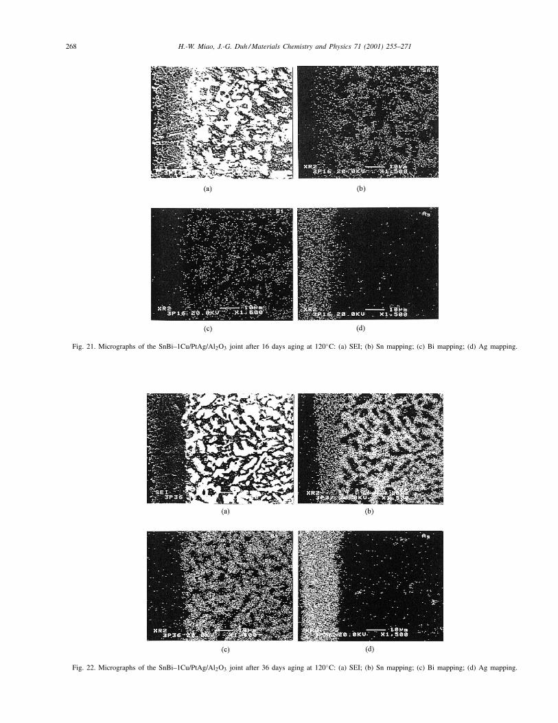
Fig. 21. Micrographs of the SnBi–1Cu/PtAg/Al2O3 joint after 16 days aging at 120◦C: (a) SEI; (b) Sn mapping; (c) Bi mapping; (d) Ag mapping.
Fig. 22. Micrographs of the SnBi–1Cu/PtAg/Al2O3 joint after 36 days aging at 120◦C: (a) SEI; (b) Sn mapping; (c) Bi mapping; (d) Ag mapping.
H.-W. Miao, J.-G. Duh / Materials Chemistry and Physics 71 (2001) 255–271 269
Fig. 23. Electron microprobe trace across the intermetallic layer of the 42Sn–58Bi/PtAg/Al2O3 assembly after aging at 120◦C for 36 days.
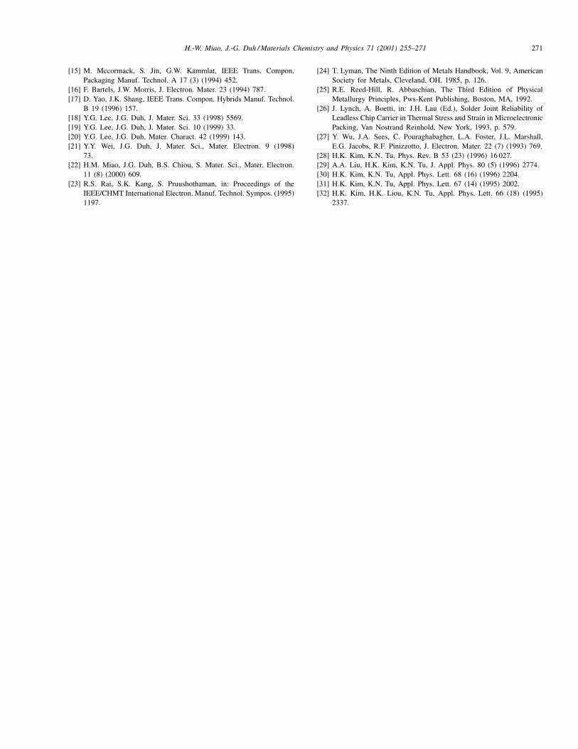
Unlike Ag3Sn, the Cu6Sn5 IMC does not form a layerat the interface between the solder and the Cu conduc-tor, instead it grows as scallop-like grains into the solder.Comparison between Figs. 14 and 22, including SEI mor-phology, Sn, Ag and Cu mapping, can reveal this discrep-ancy. Fig. 14(a) shows that the interfacial morphology forthe SnBi–1Cu/Cu/Al2O3 is rather irregular while that ofSnBi–1Cu/PtAg/Al2O3 is more or less planar, as indicatedin Fig. 22(a). The variation in the formation of Cu6Sn5 and
Fig. 24. Electron microprobe trace across the intermetallic layer of the SnBi–1Cu/PtAg/Al2O3 assembly after aging at 120◦C for 36 days.
Ag3Sn IMC in Cu metallized and PtAg metallized Al2O3substrate can be schematically represented in Fig. 26. Asimilar phenomenon was reported by Tu and co-workers[28–32], who pointed out that the scallop-like Cu6Sn5 in-termetallics were formed at the eutectic SnPb solder/Cuconductor in the molten state. The irregular growth of theCu6Sn5 compounds is caused by dissolution of Cu into themolten solder and the coarsening of the scallop-type Cu6Sn5intermetallics by Ostwald ripening.
270 H.-W. Miao, J.-G. Duh / Materials Chemistry and Physics 71 (2001) 255–271
Fig. 25. The thickness of intermetallics for the 42Sn–58Bi/PtAg/Al2O3 and the SnBi–1Cu/PtAg/Al2O3 joints vs. square root of aging time at 120◦C.
Fig. 26. Schematical diagram of IMC morphology in Ag3Sn and Cumetallized substrate.
4. Conclusions
1. A single IMC Cu6Sn5 is observed in the eutecticSnBi/Cu/FR4 joint after aging at 100◦C for 49 days, while(Cu, Ni)6Sn5 IMC is present in the SnBi/Ni/Cu/FR4joint after aging at 100◦C for 100 days.
2. Significant coarsening of the Bi-rich phase is observed inthe binary eutectic SnBi joint. However, the microstruc-ture coarsening is substantially reduced by an addition of1 wt.% Cu into the binary Sn–Bi solder. Identical trendis exhibited in the solder joined with both Cu and Pt–Agmetallized Al2O3 substrate.
3. In both SnBi/Cu/Al2O3 and SnBi–1Cu/Cu/Al2O3 joints,Cu6Sn5 IMC is formed after aging at 120◦C. However,Ag3Sn IMC is observed in both SnBi/Pt–Ag/Al2O3 andSnBi–1Cu/Pt–Ag/Al2O3 joints.
4. The formation of Ag3Sn IMC in the Sn–Bi–1Cu sol-der with PtAg metallized Al2O3 is planar, while that of
Cu6Sn5 intermetallic is the SnBi–1Cu solder with Cumetallized Al2O3 is scallop-like.
5. The growth if Ag3Sn intermetallics is diffusion con-trolled. The thickness of Ag3Sn is reduced in the ternarySnBi–1Cu/PtAg joint as compared to that in the eutecticSnBi/PtAg joint.
Acknowledgements
The authors are grateful to the financial support from Na-tional Science Council, Taiwan under the contract No. NSC86-2221-E-007-043.
References
[1] S.K. Kang, A.K. Sarkhel, J. Electron. Mater. 23 (8) (1994) 701.[2] K.C. Liu, J.G. Duh, IEEE Trans. Compon. Hybrids Manuf. Technol.
14 (4) (1991) 703.[3] P.T. Vianco, A.C. Kilgo, R. Front, J. Electron. Mater. 24 (10) (1995)
1493.[4] M. Mccormach, S. Jin, JOM 45 (7) (1993) 36.[5] M.E. Loomans, S. Zaynman, G. Gfosh, M.E. Fine, J. Electron. Mater.
23 (8) (1994) 741.[6] C.A. Mackay, W.D. Von Voss, Mater. Sci. Technol. 1 (1985) 240.[7] S. Jin, M. Mccormack, J. Electron. Mater. 23 (8) (1994) 735.[8] L.E. Felton, C.H. Raeder, D.B. Knorr, JOM 45 (7) (1993) 28.[9] J. Glazer, J. Electron. Mater. 23 (8) (1994) 693.
[10] C.H. Reader, L.E. Felton, V.A. Tanzi, D.B. Knorr, J. Electron. Mater.23 (7) (1994) 611.
[11] P.T. Vianco, D.R. Frear, JOM 45 (7) (1993) 14.[12] C.H. Reader, L.E. Felton, D.B. Knorr, G.B. Schmeelk, D. Lee,
in: Proceedings of the IEEE/CHMT Int’l Electro. Manuf. Technol.Sympos., 1993, p. 119.
[13] W.J. Tomlinson, I. Collier, J. Mater. Sci. 22 (1987) 1835.[14] Z. Mei, J.W. Morris Jr., J. Electron. Mater. 21 (6) (1992) 599.
H.-W. Miao, J.-G. Duh / Materials Chemistry and Physics 71 (2001) 255–271 271
[15] M. Mccormack, S. Jin, G.W. Kammlat, IEEE Trans. Compon.Packaging Manuf. Technol. A 17 (3) (1994) 452.
[16] F. Bartels, J.W. Morris, J. Electron. Mater. 23 (1994) 787.[17] D. Yao, J.K. Shang, IEEE Trans. Compon. Hybrids Manuf. Technol.
B 19 (1996) 157.[18] Y.G. Lee, J.G. Duh, J. Mater. Sci. 33 (1998) 5569.[19] Y.G. Lee, J.G. Duh, J. Mater. Sci. 10 (1999) 33.[20] Y.G. Lee, J.G. Duh, Mater. Charact. 42 (1999) 143.[21] Y.Y. Wei, J.G. Duh, J. Mater. Sci., Mater. Electron. 9 (1998)
73.[22] H.M. Miao, J.G. Duh, B.S. Chiou, S. Mater. Sci., Mater. Electron.
11 (8) (2000) 609.[23] R.S. Rai, S.K. Kang, S. Pruushothaman, in: Proceedings of the
IEEE/CHMT International Electron. Manuf. Technol. Sympos. (1995)1197.
[24] T. Lyman, The Ninth Edition of Metals Handbook, Vol. 9, AmericanSociety for Metals, Cleveland, OH, 1985, p. 126.
[25] R.E. Reed-Hill, R. Abbaschian, The Third Edition of PhysicalMetallurgy Principles, Pws-Kent Publishing, Boston, MA, 1992.
[26] J. Lynch, A. Boetti, in: J.H. Lau (Ed.), Solder Joint Reliability ofLeadless Chip Carrier in Thermal Stress and Strain in MicroelectronicPacking, Van Nostrand Reinhold, New York, 1993, p. 579.
[27] Y. Wu, J.A. Sees, C. Pouraghabagher, L.A. Foster, J.L. Marshall,E.G. Jacobs, R.F. Pinizzotto, J. Electron. Mater. 22 (7) (1993) 769.
[28] H.K. Kim, K.N. Tu, Phys. Rev. B 53 (23) (1996) 16 027.[29] A.A. Liu, H.K. Kim, K.N. Tu, J. Appl. Phys. 80 (5) (1996) 2774.[30] H.K. Kim, K.N. Tu, Appl. Phys. Lett. 68 (16) (1996) 2204.[31] H.K. Kim, K.N. Tu, Appl. Phys. Lett. 67 (14) (1995) 2002.[32] H.K. Kim, H.K. Liou, K.N. Tu, Appl. Phys. Lett. 66 (18) (1995)
2337.
Related Documents