Direct Memory Access (DMA) Operation and DMA Controller

Welcome message from author
This document is posted to help you gain knowledge. Please leave a comment to let me know what you think about it! Share it to your friends and learn new things together.
Transcript

Direct Memory Access (DMA) Operation and DMA Controller

Basic DMA concept
• Direct memory access (DMA) is a feature of modern computer systems that allows certain hardware subsystems to read/write data to/from memory without microprocessor intervention, allowing the processor to do other work.
• Used in disk controllers, video/sound cards etc, or between memory locations.

• Typically, the CPU initiates DMA transfer, does other operations while the transfer is in progress, and receives an interrupt from the DMA controller once the operation is complete.
• Can create cache coherency problems (the data in the cache may be different from the data in the external memory after DMA)

Basic DMA Terminology
• DMA channel: system pathway used by a device to transfer information directly to and from memory. There are usually 8 in a computer system
• DMA controller: dedicated hardware used for controlling the DMA operation

• Single-cycle mode: DMA data transfer is done one byte at a time
• Burst-mode: DMA transfer is finished when all data has been moved

DMA Pins and Timing
• x86 Interrupt Pins
– HOLD: DMA request
• Sampled in the middle of any clocking cycle
– HLDA: DMA acknowledge signal.
• The address, data and control buses are set to high-Z, so the I/O devices can control the system bus
1 2 3 4 5 6 7 8 9
CLK
HOLD
HLDA

DMA on the 8086 Microprocessor• The I/O device asserts the appropriate signal for the
channel.• The DMA controller will enable appropriate channel,
and ask the CPU to release the bus so that the DMA may use the bus. The DMA requests the bus by asserting the HOLD signal which goes to the CPU.

• The CPU detects the HOLD signal, and will complete executing the current instruction. Now all of the signals normally generated by the CPU are placed in a tri-stated condition (neither high or low) and then the CPU asserts the HLDA signal which tells the DMA controller that it is now in charge of the bus.

• The CPU may have to wait (hold cycles).• DMA activates its MEMR, MEMW, IOR, IOW output
signals, and the address outputs from the DMA are set to the target address, which will be used to direct the byte that is about to transferred to a specific memory location.

• The DMA will then let the device that requested the DMA transfer know that the transfer is commencing by asserting the DACK signal.
• The peripheral places the byte to be transferred on the bus Data lines.

• Once the data has been transferred, The DMA will de-assert the DACK2 signal.
• The DMA will now check to see if any of the other DMA channels have any work to do. If none of the channels have their DRQ lines asserted, the DMA controller has completed its work and will now tri-state the MEMR, MEMW, IOR, IOW and address signals.

• Finally, the DMA will de-assert the HOLD signal. The CPU sees this, and de-asserts the HOLDA signal. Now the CPU resumes control of the buses and address lines, and it resumes executing instructions and accessing main memory and the peripherals.

8237 DMA Controller
• Supplies memory and I/O with control signals and addresses during DMA transfer
• 4-channels (expandable)– 0: DRAM refresh– 1: Free– 2: Floppy disk controller– 3: Free

• 1.6 MByte/sec transfer rate• 64 KByte section of memory address capability
with single programming• “fly-by” controller (data does not pass through
the DMA-only memory to I/O transfer capability)• Initialization involves writing into each channel:
i) The address of the first byte of the block of data that must be transferred (called the base address). ii) The number of bytes to be transferred (called the word count).

8237 pins• CLK: System clock• CS΄: Chip select (decoder output)• RESET: Clears registers, sets mask register• READY: 0 for inserting wait states• HLDA: Signals that the μp has relinquished buses• DREQ3 – DREQ0: DMA request input for each channel• DB7-DB0: Data bus pins• IOR΄: Bidirectional pin used during programming and during a DMA write cycle• IOW΄: Bidirectional pin used during programming and during a DMA read cycle• EOP΄: End of process is a bidirectional signal used as input to terminate a DMA process or as output
to signal the end of the DMA transfer• A3-A0: Address pins for selecting internal registers• A7-A4: Outputs that provide part of the DMA transfer address• HRQ: DMA request output• DACK3-DACK0: DMA acknowledge for each channel.• AEN: Address enable signal• ADSTB: Address strobe• MEMR΄: Memory read output used in DMA read cycle• MEMW΄: Memory write output used in DMA write cycle

8237 DMA Application
8237 registers
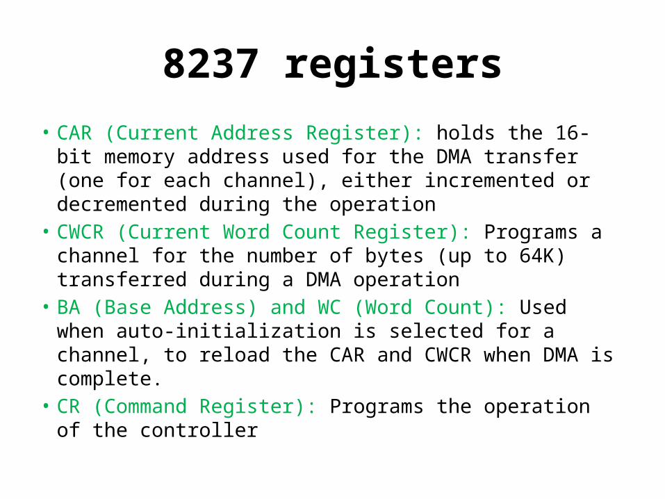
• CAR (Current Address Register): holds the 16-bit memory address used for the DMA transfer (one for each channel), either incremented or decremented during the operation
• CWCR (Current Word Count Register): Programs a channel for the number of bytes (up to 64K) transferred during a DMA operation
• BA (Base Address) and WC (Word Count): Used when auto-initialization is selected for a channel, to reload the CAR and CWCR when DMA is complete.
• CR (Command Register): Programs the operation of the controller
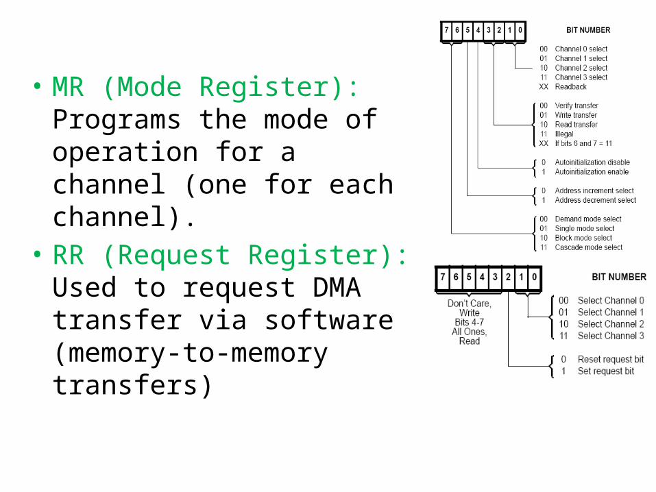
• MR (Mode Register): Programs the mode of operation for a channel (one for each channel).
• RR (Request Register): Used to request DMA transfer via software (memory-to-memory transfers)
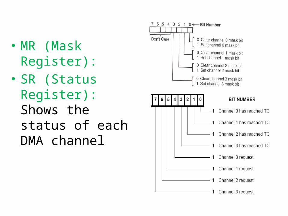
• MR (Mask Register):• SR (Status Register):
Shows the status of each DMA channel

8237 Software commands

8237 Software commands• Clear First/Last Flip-Flop - This command is executed prior to
writing or reading new address or word count information to the 82C37.
• Set First/Last Flip-Flop - This command will set the flip-flop to select the high byte first on read and write operations to address and word count registers.
• Master Clear - This software instruction has the same effect as the hardware Reset.
• Clear Mask Register - This command clears the mask bits of all four channels, enabling them to accept DMA requests.
• Clear Mode Register Counter- An internal two-bit counter has been included to select Mode registers during read operation.
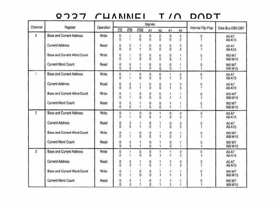
8237 CHANNEL I/O PORT ADDRESSES

8237 Block Diagram

Initiating a DMA Transaction
• Save the current interrupt status and disable interrupts • Disable the channel that will be used for the
transaction • Reset the flip-flop• Set the Mode Register • Set the Page Register • Set the Offset Register • Set the Block Size Register • Enable the channel that is used for the transaction • Restore the interrupt status

Programming the 8237• First program the address and count registers
first:1. Clear the F/L flip-flop with a clear F/L command2. Disable the channel3. Program the LSB and then MSB of the address4. Program the LSB and then MSB of the count
• Select the mode of operation• Enable channel

Example
• Design the 8237 decoding circuit and the 8237 address line connections so that the 8237 is in the address range 70h-7Fh
• Write a program that starts a block memory-to-memory DMA transfer from memory locations 10000H-13FFFH to 140000H-17FFFH using channel 0 as source and channel 1 as destination.
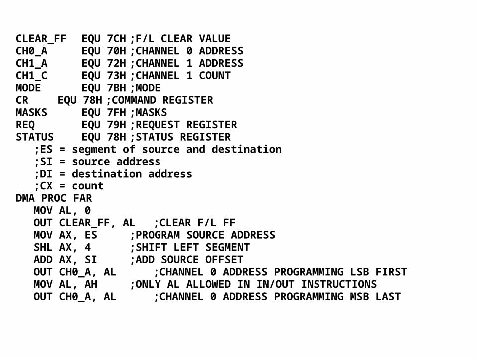
CLEAR_FF EQU 7CH ;F/L CLEAR VALUECH0_A EQU 70H ;CHANNEL 0 ADDRESSCH1_A EQU 72H ;CHANNEL 1 ADDRESSCH1_C EQU 73H ;CHANNEL 1 COUNTMODE EQU 7BH ;MODECR EQU 78H ;COMMAND REGISTERMASKS EQU 7FH ;MASKSREQ EQU 79H ;REQUEST REGISTERSTATUS EQU 78H ;STATUS REGISTER
;ES = segment of source and destination;SI = source address;DI = destination address;CX = count
DMA PROC FAR MOV AL, 0
OUT CLEAR_FF, AL ;CLEAR F/L FFMOV AX, ES ;PROGRAM SOURCE ADDRESSSHL AX, 4 ;SHIFT LEFT SEGMENTADD AX, SI ;ADD SOURCE OFFSETOUT CH0_A, AL ;CHANNEL 0 ADDRESS PROGRAMMING LSB FIRSTMOV AL, AH ;ONLY AL ALLOWED IN IN/OUT INSTRUCTIONSOUT CH0_A, AL ;CHANNEL 0 ADDRESS PROGRAMMING MSB LAST

MOV AX, ES ;PROGRAM DESTINATION ADDRESSSHL AX, 4 ;SHIFT LEFT SEGMENTADD AX, DI ;ADD DESTINATION OFFSETOUT CH1_A, AL ;CHANNEL 1 ADDRESS PROGRAMMING LSB FIRSTMOV AL, AH ;ONLY AL ALLOWED IN IN/OUT INSTRUCTIONSOUT CH1_A, AL ;CHANNEL 1 ADDRESS PROGRAMMING MSB FIRSTMOV AX, CX ;PROGRAM COUNTDEC AX ;ADJUST COUNTOUT CH1_C, AL ;MOVE TO CHANNEL 1 COUNTMOV AL, AHOUT CH1_C, AL
MOV AL, 88H ;PROGRAM MODEOUT MODE, AL
MOV AL,1 ;MEMORY-TO-MEMORY TRANSFEROUT CR, AL
MOV AL, 0EH ;UNMASK CHANNEL 0OUT MASKS, AL
MOV AL, 4 ;START DMA TRANSFER BY SETTING REQUEST BIT FOR CHANNEL 2OUT REQ, AL

Direct Memory Channel Improvement• Interrupt processing• Peripheral module to perform DMA. • Bus arbitrator.• There can only be one user of the data bus so
processor must wait if DMA is transferring data.• DMA controller tells the processor when the DMA
has completed the transfer.

DMA Block Diagram
RAM
CPU DMA Module
Address bus
Data bus
address setupExternalI/O lines
cycle state signals
Interrupt line

Sharing of the op-code cycles1. RAM access
• Read the OP code from program memory (fetch)
• Read/write data from/to data RAM addresses (decode and writeback)
2. CPU operations (execute)• Perform data manipulation • DMA device performs RAM access during
this second portion of the op-code cycle

DMA Controller in BF533• Between memory and memory (MDMA) (Memory
DMA)• Between memory and the I/O through a serial or
parallel port.• There are 12 DMA channels for various transfers. • Two ways of programming DMA transfers
– Descriptor-based– Register-based

Descriptor-based DMA• Transfers require a set of parameters stored within
memory to initiate a DMA sequence. • Allows the chaining together of multiple DMA
sequences. • DMA channel can be programmed to automatically
set up and start another DMA transfer after the current sequence completes.

Register-based DMA
• Allows the processor to directly program DMA control registers to initiate a DMA transfer.
• On completion, the control registers may be automatically updated with their original setup values for continuous transfer, if needed.

DMA RegistersDMA registers fall into three categories:• Parameter registers, such as
DMAx_CONFIG and DMAx_X_COUNT• Current registers, such as DMAx_CURR_ADDR and
DMAx_CURR_X_COUNT• Control/Status registers, such as DMAx_IRQ_STATUS
and DMAx_PERIPHERAL_MAP

Video Interface
DMA
Video source
Display Unit
BF533
VideoInPort Decoder
PPI Interface
Memory
PPI Interface
EncoderVideoOutPort
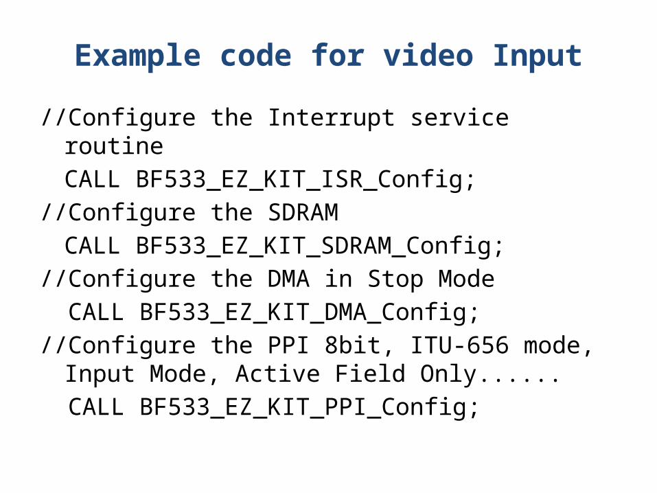
Example code for video Input
//Configure the Interrupt service routine CALL BF533_EZ_KIT_ISR_Config;
//Configure the SDRAMCALL BF533_EZ_KIT_SDRAM_Config;
//Configure the DMA in Stop Mode CALL BF533_EZ_KIT_DMA_Config;//Configure the PPI 8bit, ITU-656 mode, Input Mode, Active
Field Only...... CALL BF533_EZ_KIT_PPI_Config;

Computer System with DMA
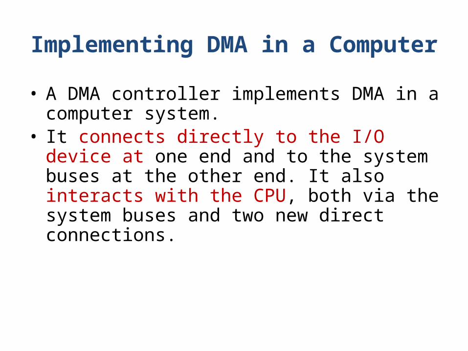
Implementing DMA in a Computer
• A DMA controller implements DMA in a computer system.
• It connects directly to the I/O device at one end and to the system buses at the other end. It also interacts with the CPU, both via the system buses and two new direct connections.
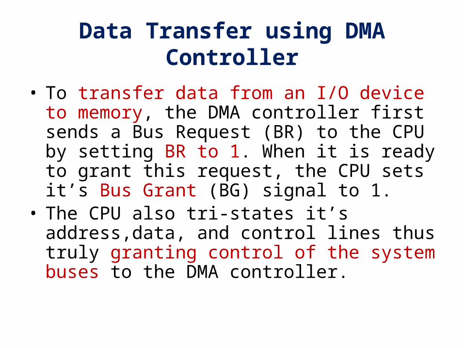
Data Transfer using DMA Controller
• To transfer data from an I/O device to memory, the DMA controller first sends a Bus Request (BR) to the CPU by setting BR to 1. When it is ready to grant this request, the CPU sets it’s Bus Grant (BG) signal to 1.
• The CPU also tri-states it’s address,data, and control lines thus truly granting control of the system buses to the DMA controller.
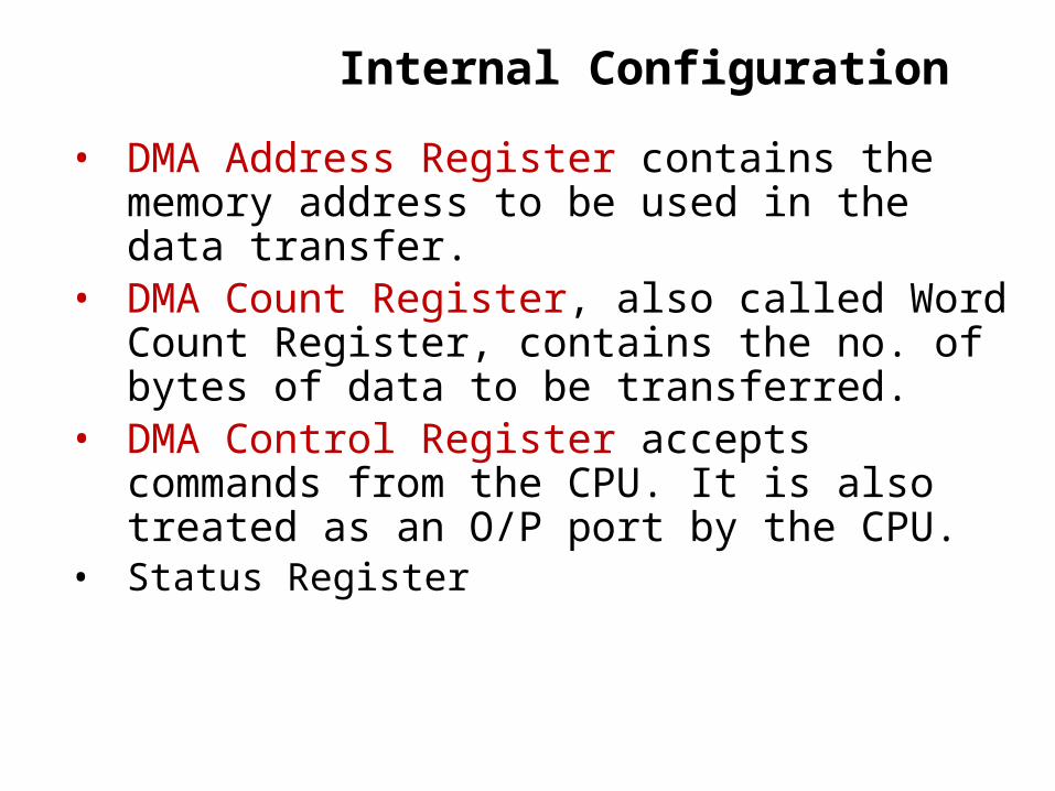
Internal Configuration• DMA Address Register contains the memory
address to be used in the data transfer. • DMA Count Register, also called Word Count
Register, contains the no. of bytes of data to be transferred.
• DMA Control Register accepts commands from the CPU. It is also treated as an O/P port by the CPU.
• Status Register

Internal Configuration of DMA Controller
Process of DMA Transfer
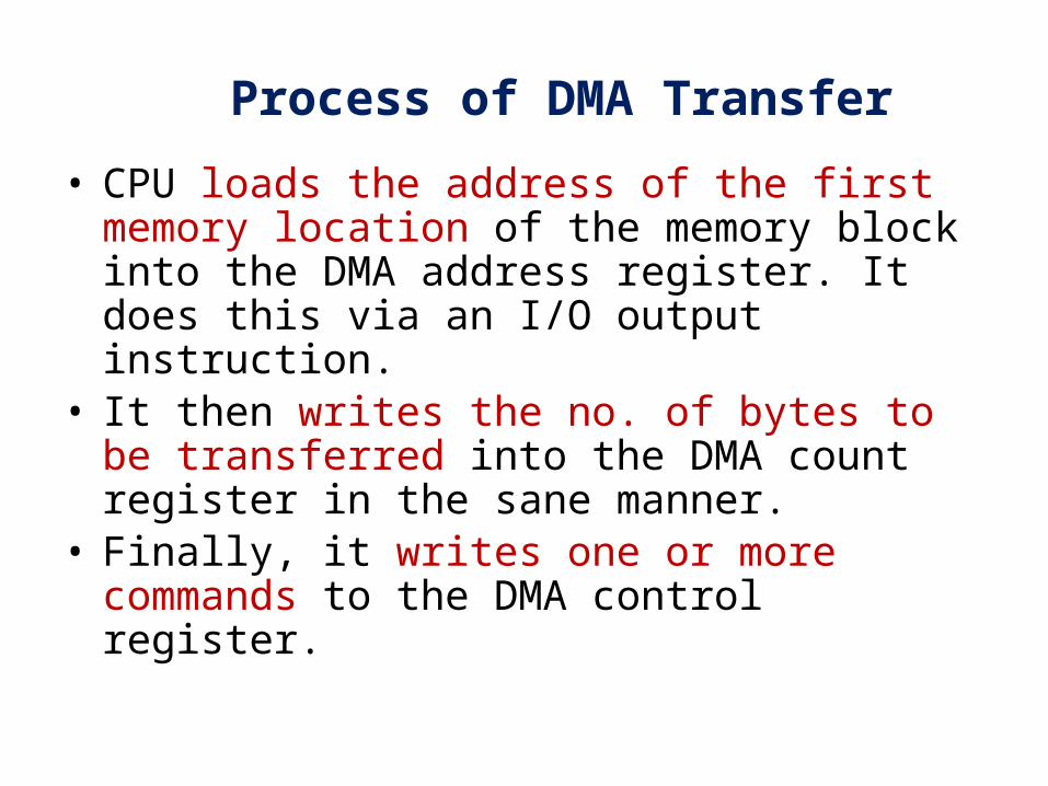
• CPU loads the address of the first memory location of the memory block into the DMA address register. It does this via an I/O output instruction.
• It then writes the no. of bytes to be transferred into the DMA count register in the sane manner.
• Finally, it writes one or more commands to the DMA control register.

• The last command causes the DMA controller to initiate the transfer. The controller then sets BR to 1 and, once BG becomes 1 , seizes control of the system buses.

DMA Transfer ModesModes vary by how the DMA controller determines when to transfer data, but the actual data transfer process is the same for all the modes. • BURST mode
– Sometimes called Block Transfer Mode.– An entire block of data is transferred in one contiguous sequence.
Once the DMA controller is granted access to the system buses by the CPU, it transfers all bytes of data in the data block before releasing control of the system buses back to the CPU.
– This mode is useful for loading programs or data files into memory, but it does render the CPU inactive for relatively long periods of time.

CYCLE STEALING Mode• Viable alternative for systems in which the
CPU should not be disabled for the length of time needed for Burst transfer modes.
• DMA controller obtains access to the system buses as in burst mode, using BR & BG signals. However, it transfers one byte of data and then deasserts BR, returning control of the system buses to the CPU.

• By continually obtaining and releasing control of the system buses, the DMA controller essentially interleaves instruction & data transfers. The CPU processes an instruction, then the DMA controller transfers a data value, and so on.
• The data block is not transferred as quickly as in burst mode, but the CPU is not idled for as long as in that mode.
• Useful for controllers monitoring data in real time.

• TRANSPARENT Mode– This requires the most time to transfer a block of data,
yet it is also the most efficient in terms of overall system performance.
– The DMA controller only transfers data when the CPU is performing operations.
– For example, the Relatively simple CPU has several states that move or process data solely within the CPU:
NOP1: (No operation) LDAC5: ACDR

JUMP3: PCDR,TR CLAC1: AC0, Z1• Primary advantage is that CPU never stops
executing its programs and DMA transfer is free in terms of time.
• Disadvantage is that the hardware needed to determine when the CPU is not using the system buses can be quite complex and relatively expensive.

Hardware Implementation of BG

Modified State Diagram To Accommodate BR and BG

Advantages of DMA
• Fast memory transfer of data• CPU and DMA run concurrently under cache mode• DMA can trigger an interrupt, which frees the CPU
from polling the channel

DMA Hardware
NET+ARM
DMA
Receive ChannelReceive Channel
PeripheralPeripheral
Transmit ChannelTransmit Channel
RAMRAM
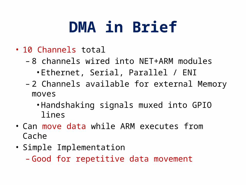
DMA in Brief• 10 Channels total
– 8 channels wired into NET+ARM modules• Ethernet, Serial, Parallel / ENI
– 2 Channels available for external Memory moves• Handshaking signals muxed into GPIO lines
• Can move data while ARM executes from Cache• Simple Implementation
– Good for repetitive data movement

Modes of Operation• Fly-by
– Data is directly transferred between memory and the peripheral
• Memory to Memory– Data is not directly transferred, but buffered in
between transfers– Data is copied from the source location into a
temporary area in the DMA channel, and then written into the destination location.

External DMA – Fly By
Memory
DMAController
Peripheral
Net+ARMA
dd
DMARequest
DMAGrant
DATA

Closer look at Fly-By Signaling
Net+ARM
DRQ*DACK*DONE*R / W*
DATA[31:0]ADDR[27:0]
CSx*
Memory
CS*ADDR[X:0]DATA[31:0]
R / W*
External Device
DRQ*EnableDoneDirectionDATA[31:0]

External DMA – Mem To Mem
Memory
DMAController Peripheral
Net+ARMA
DD
DMARequest
DMA GrantD
ATA
DATA
ADD
Holding FIFO
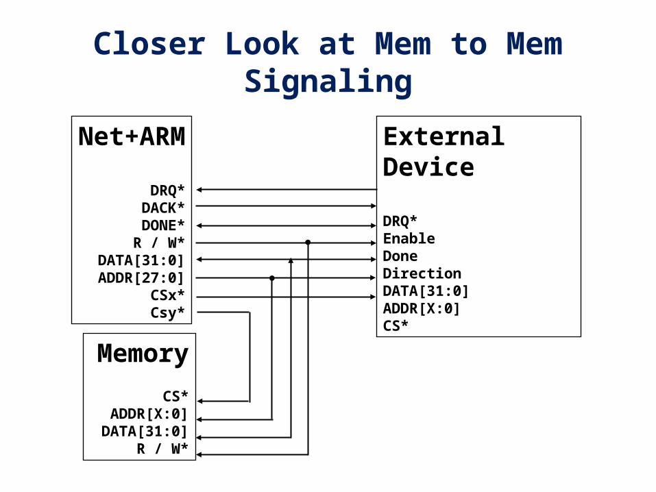
Closer Look at Mem to Mem Signaling
Net+ARM
DRQ*DACK*DONE*R / W*
DATA[31:0]ADDR[27:0]
CSx*Csy*
Memory
CS*ADDR[X:0]DATA[31:0]
R / W*
External Device
DRQ*EnableDoneDirectionDATA[31:0]ADDR[X:0]CS*
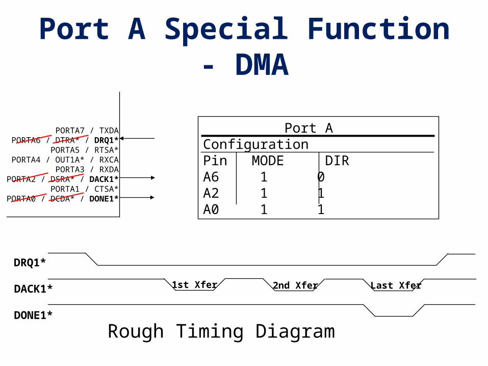
Port A Special Function - DMA
Port A ConfigurationPin MODE DIRA6 1 0A2 1 1A0 1 1
PORTA7 / TXDAPORTA6 / DTRA* / DRQ1*
PORTA5 / RTSA*PORTA4 / OUT1A* / RXCA
PORTA3 / RXDAPORTA2 / DSRA* / DACK1*
PORTA1 / CTSA*PORTA0 / DCDA* / DONE1*
DRQ1*
DACK1*
DONE1*
1st Xfer 2nd Xfer Last Xfer
Rough Timing Diagram
Related Documents


![钱币.pptx [Autosaved].pptx](https://static.cupdf.com/doc/110x72/55cf91bf550346f57b905058/pptx-autosavedpptx.jpg)