Theodoros G. Kostis MICROCONTROLLER-BASED FREQUENCY SYNTHESIS FOR MODERN COMMUNICATIONS SYSTEMS SOUTH BANK UNIVERSITY Submitted to South Bank University in partial fulfilment of the requirements for the degree of Bachelor of Engineering Department of Electrical Electronic & Information Engineering SOUTH BANK UNIVERSITY London

Welcome message from author
This document is posted to help you gain knowledge. Please leave a comment to let me know what you think about it! Share it to your friends and learn new things together.
Transcript
Theodoros G. Kostis
MICROCONTROLLER-BASEDFREQUENCY SYNTHESISFOR MODERN COMMUNICATIONSSYSTEMS
SOUTHBANKUNIVERSITY
Submitted to South Bank University in partial fulfilment ofthe requirements for the degree of Bachelor of Engineering
Department of ElectricalElectronic & InformationEngineering
SOUTH BANK UNIVERSITYLondon
FINAL YEAR PROJECT DELIVERABLE : FINAL REPORT 9750624Microcontroller-based Frequency Synthesis for Modern Communications Systems.
T. KOSTIS BEng (Hons) TeCNE. 2
2. DECLARATION
This report has been submitted for assessment towards a Bachelor of Engineering/ScienceDegree in the School of Electrical, Electronic and Information Engineering, South BankUniversity.
Author’s Signature
3. ACKNOWLEDGEMENTS
Ãéá ôïí ¸êôïñá
Ôçò Äéêáéïóýíçò ¹ëéå ÍïçôÝêáé ìõñóßíç åóý äïîáóôéêÞìç ðáñáêáëþ óáò ìçí ëçóìïíÜôå ôçí ÷þñá ìïõ.
Áåôüìïñöá ôá Ý÷åé ôá øçëÜ âïõíÜóôá çöáßóôåéá êëßìáôá óåéñÜêáé ôá óðßôéá ðéï ëåõêÜóôïý Ãëáõêïý ôï ãåéôüíåìá.
- ÏäõóóÝáò Åëýôçò.
Ôïí Üíôñá ôïí ðïëýôñïðï ðåò ìïõ, èåÜ, ðïõ ÷ñüíéáðáñÜäåñíå, óáí ðÜôçóå ôçò Ôñïßáò ô’ Üãéï êÜóôñï,êé áíèñþðùí ãíþñéóå ðïëëþí ôïõò ôüðïõò êáé ôç ãíþìçêé Ýðáèå ðëÞèïò óõìöïñÝò óôá ðÝëáãá, æçôþíôáòðþò óôçí ðáôñßäá ôïõ íá ðÜåé ìå ôïõò óõíôñüöïõò.
- ÏìÞñïõ Ïäýóóåéá, Óôß÷ïò 1-5.
This project would not have been possible without the consistent advice and constantsupport of Dr Goran Bezanov in the Embedded Systems Department, South Bank University,who also acted as the supervisor of this project.
Further appreciation comments Alan Nigrin at the Communications Laboratory for his vitalcontribution to the final testing phase.
Special thanks go to my lifelong friends P. Delimaras, G. Koutsoulis and K. Pliakos and K.Kefalas. Especially without the first I wouldn’t have a degree now.
Finally I wish to thank my father George, my mother Maria and my sister Lilla in Athens,Greece for being the wonderful people they are.
FINAL YEAR PROJECT DELIVERABLE : FINAL REPORT 9750624Microcontroller-based Frequency Synthesis for Modern Communications Systems.
T. KOSTIS BEng (Hons) TeCNE. 3
4. ABSTRACT
This project demonstrates the use of a Direct Digital Synthesis device in order to generatestable sinusoidal waveforms in the 1 to 72 MHz band that can be used as Local Oscillatorblocks in modern transceiver systems. Moreover the experimental part of the project provesthat DDS components can be programmed in a purely digital manner from a mastermicrocontroller or digital signal processor. The results of this project can be used to constructa high-speed switching transceiver according to the concept of spread spectrumcommunications.
FINAL YEAR PROJECT DELIVERABLE : FINAL REPORT 9750624Microcontroller-based Frequency Synthesis for Modern Communications Systems.
T. KOSTIS BEng (Hons) TeCNE. 4
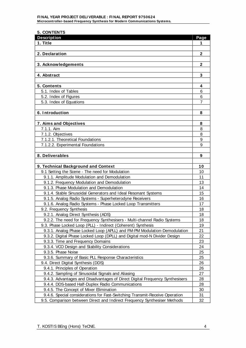
5. CONTENTSDescription Page1. Title 1
2. Declaration 2
3. Acknowledgements 2
4. Abstract 3
5. Contents 4 5.1. Index of Tables 6 5.2. Index of Figures 6 5.3. Index of Equations 7
6. Introduction 8
7. Aims and Objectives 8 7.1.1. Aim 8 7.1.2. Objectives 8 7.1.2.1. Theoretical Foundations 9 7.1.2.2. Experimental Foundations 9
8. Deliverables 9
9. Technical Background and Context 10 9.1 Setting the Scene - The need for Modulation 10 9.1.1. Amplitude Modulation and Demodulation 11 9.1.2. Frequency Modulation and Demodulation 13 9.1.3. Phase Modulation and Demodulation 14 9.1.4. Stable Sinusoidal Generators and Ideal Resonant Systems 15 9.1.5. Analog Radio Systems - Superheterodyne Receivers 16 9.1.6. Analog Radio Systems - Phase Locked Loop Transmitters 17 9.2. Frequency Synthesis 18 9.2.1. Analog Direct Synthesis (ADS) 18 9.2.2. The need for Frequency Synthesisers - Multi-channel Radio Systems 18 9.3. Phase Locked Loop (PLL) - Indirect (Coherent) Synthesis 19 9.3.1. Analog Phase Locked Loop (APLL) and FM-PM Modulation-Demodulation 21 9.3.2. Digital Phase Locked Loop (DPLL) and Digital mod-N Divider Design 22 9.3.3. Time and Frequency Domains 23 9.3.4. VCO Design and Stability Considerations 24 9.3.5. Phase Noise 25 9.3.6. Summary of Basic PLL Response Characteristics 25 9.4. Direct Digital Synthesis (DDS) 26 9.4.1. Principles of Operation 26 9.4.2. Sampling of Sinusoidal Signals and Aliasing 27 9.4.3. Advantages and Disadvantages of Direct Digital Frequency Synthesisers 28 9.4.4. DDS-based Half-Duplex Radio Communications 28 9.4.5. The Concept of Mixer Elimination 30 9.4.6. Special considerations for Fast-Switching Transmit-Receive Operation 31 9.5. Comparison between Direct and Indirect Frequency Synthesiser Methods 32
FINAL YEAR PROJECT DELIVERABLE : FINAL REPORT 9750624Microcontroller-based Frequency Synthesis for Modern Communications Systems.
T. KOSTIS BEng (Hons) TeCNE. 5
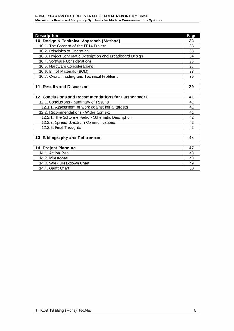
Description Page10. Design & Technical Approach (Method) 33 10.1. The Concept of the FB14 Project 33 10.2. Principles of Operation 33 10.3. Project Schematic Description and Breadboard Design 34 10.4. Software Considerations 36 10.5. Hardware Considerations 37 10.6. Bill of Materials (BOM) 38 10.7. Overall Testing and Technical Problems 39
11. Results and Discussion 39
12. Conclusions and Recommendations for Further Work 41 12.1. Conclusions - Summary of Results 41 12.1.1. Assessment of work against initial targets 41 12.2. Recommendations - Wider Context 41 12.2.1. The Software Radio - Schematic Description 42 12.2.2. Spread Spectrum Communications 42 12.2.3. Final Thoughts 43
13. Bibliography and References 44
14. Project Planning 47 14.1. Action Plan 48 14.2. Milestones 48 14.3. Work Breakdown Chart 49 14.4. Gantt Chart 50
FINAL YEAR PROJECT DELIVERABLE : FINAL REPORT 9750624Microcontroller-based Frequency Synthesis for Modern Communications Systems.
T. KOSTIS BEng (Hons) TeCNE. 6
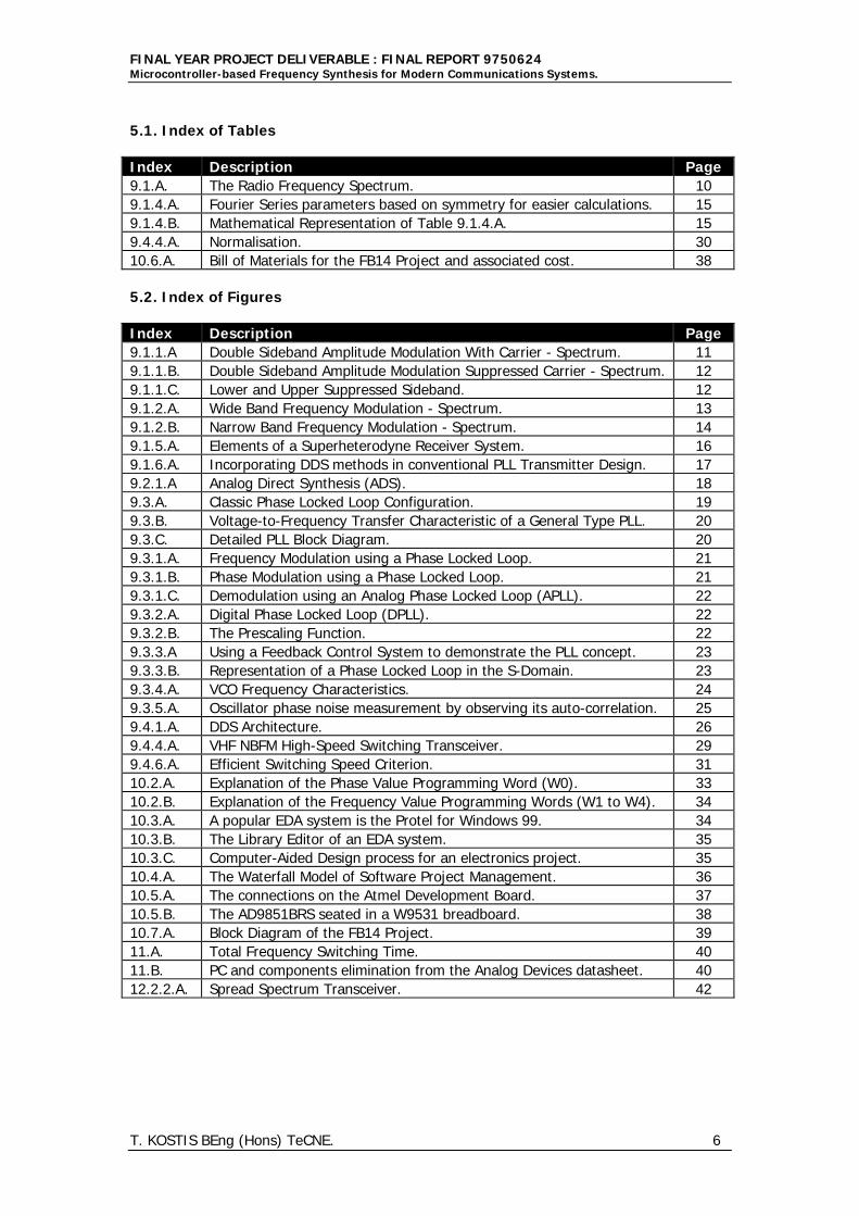
5.1. Index of Tables
Index Description Page9.1.A. The Radio Frequency Spectrum. 109.1.4.A. Fourier Series parameters based on symmetry for easier calculations. 159.1.4.B. Mathematical Representation of Table 9.1.4.A. 159.4.4.A. Normalisation. 3010.6.A. Bill of Materials for the FB14 Project and associated cost. 38
5.2. Index of Figures
Index Description Page9.1.1.A Double Sideband Amplitude Modulation With Carrier - Spectrum. 119.1.1.B. Double Sideband Amplitude Modulation Suppressed Carrier - Spectrum. 129.1.1.C. Lower and Upper Suppressed Sideband. 129.1.2.A. Wide Band Frequency Modulation - Spectrum. 139.1.2.B. Narrow Band Frequency Modulation - Spectrum. 149.1.5.A. Elements of a Superheterodyne Receiver System. 169.1.6.A. Incorporating DDS methods in conventional PLL Transmitter Design. 179.2.1.A Analog Direct Synthesis (ADS). 189.3.A. Classic Phase Locked Loop Configuration. 199.3.B. Voltage-to-Frequency Transfer Characteristic of a General Type PLL. 209.3.C. Detailed PLL Block Diagram. 209.3.1.A. Frequency Modulation using a Phase Locked Loop. 219.3.1.B. Phase Modulation using a Phase Locked Loop. 219.3.1.C. Demodulation using an Analog Phase Locked Loop (APLL). 229.3.2.A. Digital Phase Locked Loop (DPLL). 229.3.2.B. The Prescaling Function. 229.3.3.A Using a Feedback Control System to demonstrate the PLL concept. 239.3.3.B. Representation of a Phase Locked Loop in the S-Domain. 239.3.4.A. VCO Frequency Characteristics. 249.3.5.A. Oscillator phase noise measurement by observing its auto-correlation. 259.4.1.A. DDS Architecture. 269.4.4.A. VHF NBFM High-Speed Switching Transceiver. 299.4.6.A. Efficient Switching Speed Criterion. 3110.2.A. Explanation of the Phase Value Programming Word (W0). 3310.2.B. Explanation of the Frequency Value Programming Words (W1 to W4). 3410.3.A. A popular EDA system is the Protel for Windows 99. 3410.3.B. The Library Editor of an EDA system. 3510.3.C. Computer-Aided Design process for an electronics project. 3510.4.A. The Waterfall Model of Software Project Management. 3610.5.A. The connections on the Atmel Development Board. 3710.5.B. The AD9851BRS seated in a W9531 breadboard. 3810.7.A. Block Diagram of the FB14 Project. 3911.A. Total Frequency Switching Time. 4011.B. PC and components elimination from the Analog Devices datasheet. 4012.2.2.A. Spread Spectrum Transceiver. 42
FINAL YEAR PROJECT DELIVERABLE : FINAL REPORT 9750624Microcontroller-based Frequency Synthesis for Modern Communications Systems.
T. KOSTIS BEng (Hons) TeCNE. 7
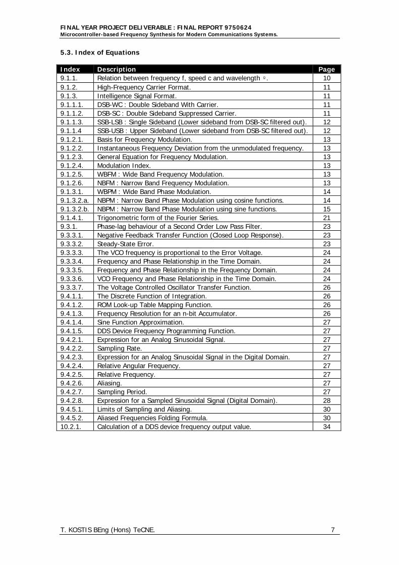
5.3. Index of Equations
Index Description Page9.1.1. Relation between frequency f, speed c and wavelength ë. 109.1.2. High-Frequency Carrier Format. 119.1.3. Intelligence Signal Format. 119.1.1.1. DSB-WC : Double Sideband With Carrier. 119.1.1.2. DSB-SC : Double Sideband Suppressed Carrier. 119.1.1.3. SSB-LSB : Single Sideband (Lower sideband from DSB-SC filtered out). 129.1.1.4 SSB-USB : Upper Sideband (Lower sideband from DSB-SC filtered out). 129.1.2.1. Basis for Frequency Modulation. 139.1.2.2. Instantaneous Frequency Deviation from the unmodulated frequency. 139.1.2.3. General Equation for Frequency Modulation. 139.1.2.4. Modulation Index. 139.1.2.5. WBFM : Wide Band Frequency Modulation. 139.1.2.6. NBFM : Narrow Band Frequency Modulation. 139.1.3.1. WBPM : Wide Band Phase Modulation. 149.1.3.2.a. NBPM : Narrow Band Phase Modulation using cosine functions. 149.1.3.2.b. NBPM : Narrow Band Phase Modulation using sine functions. 159.1.4.1. Trigonometric form of the Fourier Series. 219.3.1. Phase-lag behaviour of a Second Order Low Pass Filter. 239.3.3.1. Negative Feedback Transfer Function (Closed Loop Response). 239.3.3.2. Steady-State Error. 239.3.3.3. The VCO frequency is proportional to the Error Voltage. 249.3.3.4. Frequency and Phase Relationship in the Time Domain. 249.3.3.5. Frequency and Phase Relationship in the Frequency Domain. 249.3.3.6. VCO Frequency and Phase Relationship in the Time Domain. 249.3.3.7. The Voltage Controlled Oscillator Transfer Function. 269.4.1.1. The Discrete Function of Integration. 269.4.1.2. ROM Look-up Table Mapping Function. 269.4.1.3. Frequency Resolution for an n-bit Accumulator. 269.4.1.4. Sine Function Approximation. 279.4.1.5. DDS Device Frequency Programming Function. 279.4.2.1. Expression for an Analog Sinusoidal Signal. 279.4.2.2. Sampling Rate. 279.4.2.3. Expression for an Analog Sinusoidal Signal in the Digital Domain. 279.4.2.4. Relative Angular Frequency. 279.4.2.5. Relative Frequency. 279.4.2.6. Aliasing. 279.4.2.7. Sampling Period. 279.4.2.8. Expression for a Sampled Sinusoidal Signal (Digital Domain). 289.4.5.1. Limits of Sampling and Aliasing. 309.4.5.2. Aliased Frequencies Folding Formula. 3010.2.1. Calculation of a DDS device frequency output value. 34
FINAL YEAR PROJECT DELIVERABLE : FINAL REPORT 9750624Microcontroller-based Frequency Synthesis for Modern Communications Systems.
T. KOSTIS BEng (Hons) TeCNE. 8
6. INTRODUCTION
The main theory behind modern radio communications is the concept of the FrequencySynthesiser. It is an active electronic device that accepts some reference frequency and thengenerates other frequencies ideally in a stable, accurate and spectral pure manner.
A common method to implement Frequency Synthesisers is the Phase Locked Loop (PLL).The Phase Locked Loop can be described as a feedback control system. Its main function isto perform signal synchronisation. It compares its input signal with its output signal andwhen the values are different it forces the output signal to follow the input. This functionusually involves some undesirable transition time.
But existing firmware and hardware solutions for two-way radio communications based solelyon analog or digital Phase Locked Loop (PLL) technologies are inefficient. The maindisadvantage is the high number of components needed that expand the board size (formfactor) of the device. Moreover these components are greatly affected by temperaturechanges and component ageing. Therefore systems with a low count of equipment andimpervious to environmental changes and component ageing are needed to realise a designwith a low overall cost of manufacture and ownership.
Recent developments in stable sinusoidal signal generation without the need for a feedbackcontrol system are in the form of Direct Digital Synthesis (DDS). Becker (1997) [4] informsthat although the theory of DDS has been around since the 1970’s it is now that small formfactor and low power integrated chipsets are widely available. On the other hand DDSsolutions cannot provide as of yet the necessary frequencies for UHF and onwards bands.
A potential solution would be a Digital Signal Processing Microprocessor (DSP ìP) basedsystem that drives the corresponding DDS circuitry to provide the appropriate RadioFrequency (RF) output levels. Another terminology for the above is Software Radio.
It is the experimental part of this project that will try to emulate the programming (loading)functions of the DSP ìP by replacing it with an 8051 compatible microcontroller.
Finally the short name of this project is FB14.
7. AIMS AND OBJECTIVES
For clarity reasons the FB14 project has one aim and two objectives.
7.1.1. AIM
The aim of the project is to analyse the theory and experimental response of Direct DigitalFrequency Synthesis (DDFS) methods, especially the sine wave generation from an AD9851Complete Direct Digital Synthesis integrated chip. Analytically its application as a frequencysynthesiser for two-way radio communications will be emphasised.
7.1.2. OBJECTIVES
There are two major objectives to be reached. First the theoretical background of frequencysynthesiser methodologies is presented in the context part of this report. And then theexperimental part demonstrates the construction and programming of a Direct Digital Devicethat can be used as a standalone frequency synthesiser or even as part of a Phase LockedLoop system.

FINAL YEAR PROJECT DELIVERABLE : FINAL REPORT 9750624Microcontroller-based Frequency Synthesis for Modern Communications Systems.
T. KOSTIS BEng (Hons) TeCNE. 9
7.1.2.1. To provide relevant theoretical foundations for the project.
The most important property that a modern communications system should possess is theability to change frequencies in a fast and reliable manner. This attribute is of paramountimportance in applications like radar array systems and spread spectrum transceiver stations.The implementation of the above systems was done by the method of Analog DirectSynthesis (ADS). But this method involves slow frequency transition speeds and largeequipment dimensions making it definitely insufficient for twenty-first century applications.
Miller (1999) [3] claims that the next implementation step should deeply involve the methodof Digital Direct Synthesis (DDS). Therefore extensive coverage of DDS Direct DigitalSynthesis based frequency synthesisers (DDFS) and their role in modern communicationssystems will be presented in this report. Specifically the AD9851BRS chip will be investigatedcoupled with the AT89S8252 Atmel microcontroller.
Direct Digital Synthesis (DDS) devices complement Phase Locked Loop (PLL) feedbackcontrol systems. Because currently existing DDS realisations cannot cover many applicationdemands for the upper Part of the frequency spectrum above 900 MHz. Therefore the theorybehind PLL systems will also be presented as a solid foundation to the findings of this report.
7.1.2.2. To provide relevant experimental foundations for the project.
The firmware and hardware part of the project involves the programming of an AtmelAT89S8252 microcontroller device as a master controller for the AD9851BRS direct digitalfrequency synthesis device. Moreover detailed software documentation using a standardmethod of software description (UML) will be attached in the appendices of the report.
Reis (1996) [7] informs that Surface Mount Device (SMD) breadboarding was deemedimpossible just a few years ago. This project presents a cheap and reliable way tobreadboard these most important components which can be as small as a needle’s eye.
The design of the schematics was done with Protel for WindowsTM Version 2.0 SchematicCapturing System. Certain component blueprints were created especially for this project sinceit deals with devices that are newly introduced in the market.
Finally the output of the AD9851BRS using an oscilloscope, a spectrum analyser or afrequency counter will be investigated and documented.
8. DELIVERABLES
• Interim Report showing the agreed line of action between the author and the supervisor.
• Software in assembly low-level language and/or C high-level language to program theAT89S8252 for bursting the control word to the AD9851.
• Proof that the program works as expected via software simulators and development board
readings. • Progress Logbook keeping a complete record of all work. • Final Report.
• Appendices with source code and UML documentation.
FINAL YEAR PROJECT DELIVERABLE : FINAL REPORT 9750624Microcontroller-based Frequency Synthesis for Modern Communications Systems.
T. KOSTIS BEng (Hons) TeCNE. 10
9. TECHNICAL BACKGROUND AND CONTEXT
An attempt is made in this section to ease the reader into the basic ideas and principles thatsurround the FB14 project. First the scene is set by examining the need for the concept ofmodulation. Then the three major analog modulation implementation methods arepresented. In the second part the concept of frequency synthesis is used to explain the basisfor multi-channel radio systems. In the third part the concept of the Phase Locked Loop isintroduced in order to provide the main theoretical foundations for modern frequencysynthesiser systems. In the fourth part the concept of Direct Digital Synthesis is extensivelyexplained. After all this project mainly deals with DDS principles and operations. Also aneffort is made to argue a new digital method of demodulation that eliminates all needs for amixer device. Moreover this part emphasises the need for a very fast switching frequencysynthesiser that are employed in applications like cellular telephony and mobile radionetworks in general. In the fifth and final part of this section a comparison is presentedbetween purely direct and indirect frequency synthesiser implementation methodologies.
9.1. Setting the Scene - The need for Modulation.
The frequency of the human voice in its original form is very low, usually in the range of 300to 3000 Hz. Let us take for example the propagation of voice through free space. Riddler(1998) [27] has given that the mathematical formula that relates frequency f, speed c andwavelength ë is :
f= cl (9.1.1)
By substituting the value for frequency f for 2000 Hz, in free space with speed of light equalto 3x10⁸ we obtain 150000 metres for the wavelength ë. Now in order to be able to transmita human baseband signal via any electronic equipment means a quarter wavelength antenna(ë/4)would be demanded or 37500 meters long. It is evident that the electronic equipmentwould be very difficult to be designed for such a wavelength application.
In order to produce a radio that would perform well in the air medium the concept ofmodulation has to be employed. Modulation is the process by which the frequency value ofthe intelligence signal containing the information is increased with the help of another signalof a much higher frequency than the human voice called the carrier. The carrier is a radiowave of constant amplitude, frequency and phase at the appropriate band of operation,either for radio, television or any other communications system.
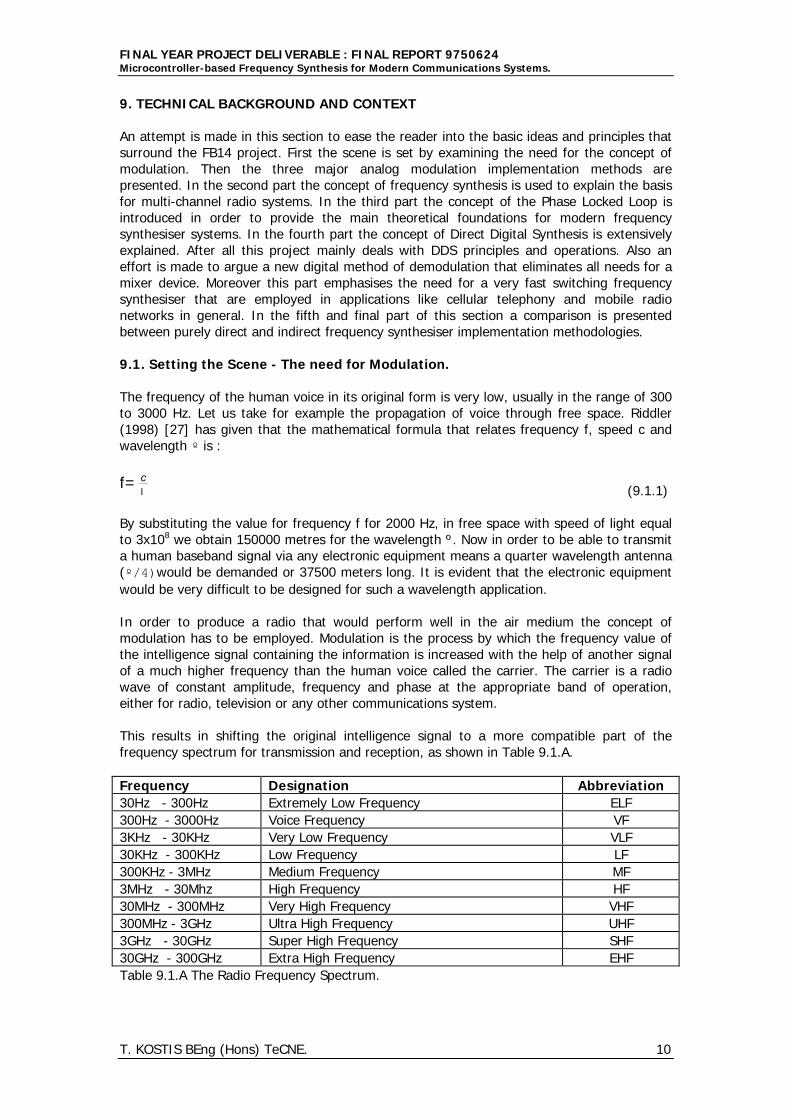
This results in shifting the original intelligence signal to a more compatible part of thefrequency spectrum for transmission and reception, as shown in Table 9.1.A.
Frequency Designation Abbreviation30Hz - 300Hz Extremely Low Frequency ELF300Hz - 3000Hz Voice Frequency VF3KHz - 30KHz Very Low Frequency VLF30KHz - 300KHz Low Frequency LF300KHz - 3MHz Medium Frequency MF3MHz - 30Mhz High Frequency HF30MHz - 300MHz Very High Frequency VHF300MHz - 3GHz Ultra High Frequency UHF3GHz - 30GHz Super High Frequency SHF30GHz - 300GHz Extra High Frequency EHFTable 9.1.A The Radio Frequency Spectrum.
FINAL YEAR PROJECT DELIVERABLE : FINAL REPORT 9750624Microcontroller-based Frequency Synthesis for Modern Communications Systems.
T. KOSTIS BEng (Hons) TeCNE. 11
For everyday communication needs the VHF and UHF bands are employed because of theintrinsic permittivity and permeability of the air medium. Moreover lower frequency radiosystems perform well in undersea communications. And higher frequency systems thatdemand line of sight for proper performance are found in satellite communications.
There are certain methods of modulation. Three analog modulation methods will be brieflyinvestigated in the following three paragraphs. The full derivation of these formulas is out ofthe scope of this report, but a very good analysis can be found in Pearson (1992) [11]. Thecommon factor that they were chosen to appear is that in their form they can easily show thespectrum of each representative method of analog modulation. The following conventionsare used :
The High-Frequency Carrier is of the form : vc=Vccoswc t (9.1.2)
The Intelligence Signal is of the form : vm =Vm coswm t (9.1.3)
The modulation and demodulation of amplitude, frequency and phase of analog signalsfollows in the text below. Moreover this report looks at a modern transceiver from a systemsperspective. Therefore emphasis is being given mostly to block diagrams and theirinteraction with each other than to the technical implementation of each building block.
9.1.1 Amplitude Modulation and Demodulation
The instantaneous changes in the amplitude of the intelligence signal proportionally affectthe reference amplitude of the high-frequency carrier. The extra frequency componentsgenerated, called sidebands, contain the information. There are three general types ofAmplitude Modulation according to their transmission power and bandwidth requirements.
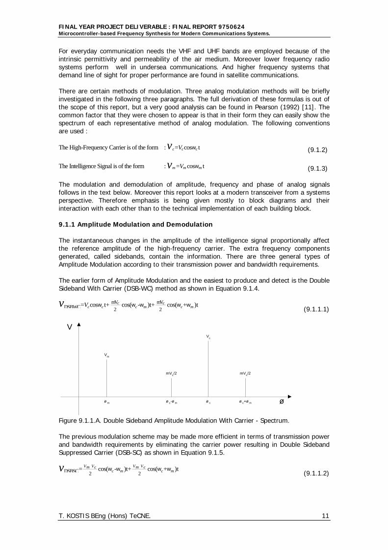
The earlier form of Amplitude Modulation and the easiest to produce and detect is the DoubleSideband With Carrier (DSB-WC) method as shown in Equation 9.1.4.
vDSBWC=Vccoswc t+ mVc
2cos(wc-wm )t+ mVc
2cos(wc+wm )t
(9.1.1.1)
Vm
mVc/2
ø m ø c-ø m ø c ø c+ø m
Vc
mVc/2
ø
V
Figure 9.1.1.A. Double Sideband Amplitude Modulation With Carrier - Spectrum.
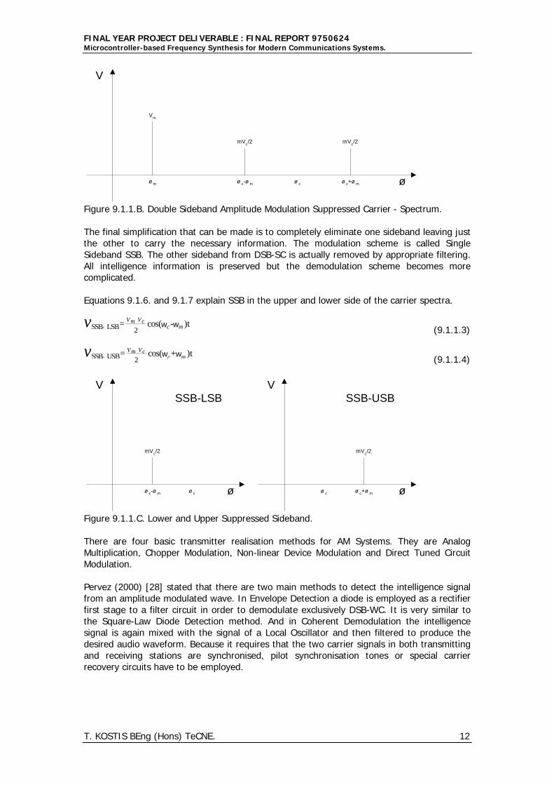
The previous modulation scheme may be made more efficient in terms of transmission powerand bandwidth requirements by eliminating the carrier power resulting in Double SidebandSuppressed Carrier (DSB-SC) as shown in Equation 9.1.5.
vDSBSC= Vm Vc
2cos(wc-wm )t+ Vm Vc
2cos(wc+wm )t
(9.1.1.2)
FINAL YEAR PROJECT DELIVERABLE : FINAL REPORT 9750624Microcontroller-based Frequency Synthesis for Modern Communications Systems.
T. KOSTIS BEng (Hons) TeCNE. 12
Vm
mVc/2
ø m ø c-ø m ø c ø c+ø m
mVc/2
ø
V
Figure 9.1.1.B. Double Sideband Amplitude Modulation Suppressed Carrier - Spectrum.
The final simplification that can be made is to completely eliminate one sideband leaving justthe other to carry the necessary information. The modulation scheme is called SingleSideband SSB. The other sideband from DSB-SC is actually removed by appropriate filtering.All intelligence information is preserved but the demodulation scheme becomes morecomplicated.
Equations 9.1.6. and 9.1.7 explain SSB in the upper and lower side of the carrier spectra.
vSSB- LSB= Vm Vc
2cos(wc-wm )t
(9.1.1.3)
vSSB- USB= Vm Vc
2cos(wc+wm )t
(9.1.1.4)
mVc/2
ø c-ø m ø c ø c+ø m
mVc/2
ø
V
ø
V
ø c
SSB-USBSSB-LSB
Figure 9.1.1.C. Lower and Upper Suppressed Sideband.
There are four basic transmitter realisation methods for AM Systems. They are AnalogMultiplication, Chopper Modulation, Non-linear Device Modulation and Direct Tuned CircuitModulation.
Pervez (2000) [28] stated that there are two main methods to detect the intelligence signalfrom an amplitude modulated wave. In Envelope Detection a diode is employed as a rectifierfirst stage to a filter circuit in order to demodulate exclusively DSB-WC. It is very similar tothe Square-Law Diode Detection method. And in Coherent Demodulation the intelligencesignal is again mixed with the signal of a Local Oscillator and then filtered to produce thedesired audio waveform. Because it requires that the two carrier signals in both transmittingand receiving stations are synchronised, pilot synchronisation tones or special carrierrecovery circuits have to be employed.
FINAL YEAR PROJECT DELIVERABLE : FINAL REPORT 9750624Microcontroller-based Frequency Synthesis for Modern Communications Systems.
T. KOSTIS BEng (Hons) TeCNE. 13
9.1.2 Frequency Modulation and Demodulation
The instantaneous changes in the amplitude of the intelligence signal proportionally andlinearly affect the frequency around the reference frequency of the high-frequency carrier.The basic principle is that the baseband intelligence signal is related to the frequencychanges by Equation 9.1.8.
äùc=Kum (9.1.2.1)
K is the modulation sensitivity measured in units of radians per Voltseconds or KHz permillivolts. And äùc is the amount by which the baseband has caused the instantaneouscarrier frequency ùi to deviate from the unmodulated frequency ùc as shown in Equation9.1.9.
ùi = ùc + äùc (9.1.2.2)
Therefore the general equation for frequency modulation is as follows :
uFM=Vccos(wc t+KÙ0tum d t ) (9.1.2.3)
And the modulation index is designated as in Equation 9.1.2.4.
b= Dwwm
= Dffm (9.1.2.4)
When the value of â is equal or larger than 0.2 Wide Band Frequency Modulation (WBFM)occurs as follows :
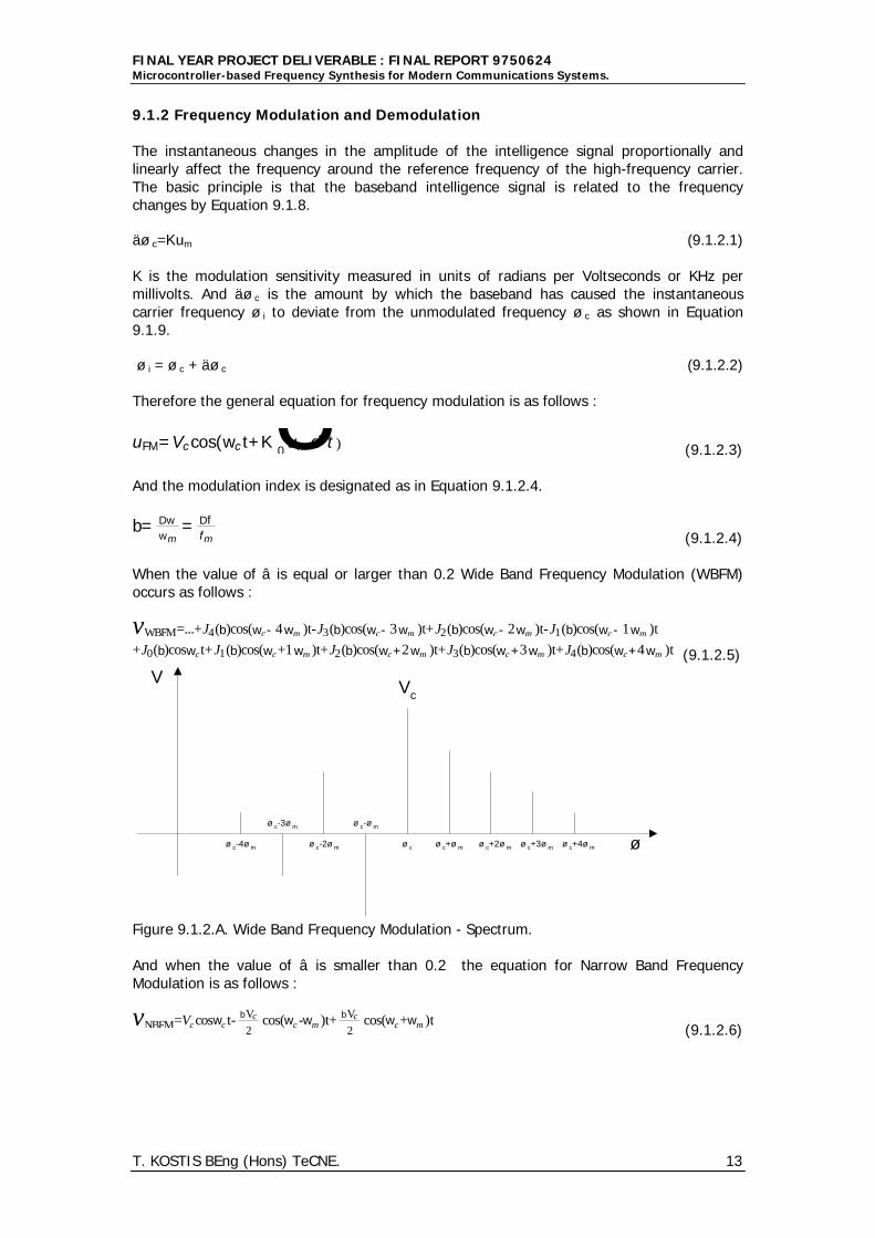
vWBFM=...+J4(b)cos(wc- 4 wm )t-J3(b)cos(wc- 3 wm )t+J2(b)cos(wc - 2 wm )t-J1(b)cos(wc - 1 wm )t
+J0(b)coswct+J1(b)cos(wc+1 wm )t+J2(b)cos(wc+2 wm )t+J3(b)cos(wc+3 wm )t+J4(b)cos(wc+4 wm )t (9.1.2.5)
ø c+ø m ø
V
ø c
ø c-ø m
Vc
ø c-2ø m ø c+2ø m ø c+3ø m ø c+4ø m
ø c-3ø m
ø c-4ø m
Figure 9.1.2.A. Wide Band Frequency Modulation - Spectrum.
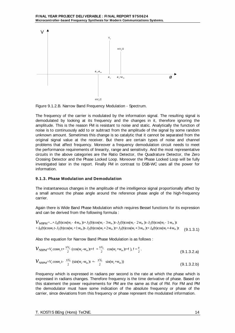
And when the value of â is smaller than 0.2 the equation for Narrow Band FrequencyModulation is as follows :
vNBFM=Vccoswc t- bVc
2cos(wc-wm )t+ bVc
2cos(wc+wm )t
(9.1.2.6)
FINAL YEAR PROJECT DELIVERABLE : FINAL REPORT 9750624Microcontroller-based Frequency Synthesis for Modern Communications Systems.
T. KOSTIS BEng (Hons) TeCNE. 14
ø c+ø m
mVc/2
ø
V
ø c
ø c-ø m
mVc/2
Vc
Figure 9.1.2.B. Narrow Band Frequency Modulation - Spectrum.
The frequency of the carrier is modulated by the information signal. The resulting signal isdemodulated by looking at its frequency and the changes in it, therefore ignoring theamplitude. This is the reason FM is resistant to noise and static. Analytically the function ofnoise is to continuously add to or subtract from the amplitude of the signal by some randomunknown amount. Sometimes this change is so catalytic that it cannot be separated from theoriginal signal value at the receiver. But there are certain types of noise and channelproblems that affect frequency. Moreover a frequency demodulation circuit needs to meetthe performance requirements of linearity, range and sensitivity. And the most representativecircuits in the above categories are the Ratio Detector, the Quadrature Detector, the ZeroCrossing Detector and the Phase Locked Loop. Moreover the Phase Locked Loop will be fullyinvestigated later in the report. Finally FM in contrast to DSB-WC uses all the power forinformation.
9.1.3. Phase Modulation and Demodulation
The instantaneous changes in the amplitude of the intelligence signal proportionally affect bya small amount the phase angle around the reference phase angle of the high-frequencycarrier.
Again there is Wide Band Phase Modulation which requires Bessel functions for its expressionand can be derived from the following formula :
vWBPM=...+J4(b)cos(wc- 4 wm )t+J3(b)cos(wc - 3 wm )t-J2(b)cos(wc- 2 wm )t-J1(b)cos(wc- 1 wm )t
+J0(b)coswct-J1(b)cos(wc+1 wm )t-J2(b)cos(wc+2 wm )t+J3(b)cos(wc+3 wm )t+J4(b)cos(wc+4 wm )t (9.1.3.1)
Also the equation for Narrow Band Phase Modulation is as follows :
vNBPM=Vccoswc t+bVc
2(cos(wc-wm )t+fL+ bVc
2 Hcos(wc+wm )t+f ), f = p
2.
(9.1.3.2.a)
vNBPM=Vccoswc t- bVc
2(sin(wc-wm )tL+- bVc
2 Hsin(wc+wm ))
(9.1.3.2.b)
Frequency which is expressed in radians per second is the rate at which the phase which isexpressed in radians changes. Therefore frequency is the time derivative of phase. Based onthis statement the power requirements for PM are the same as that of FM. For FM and PMthe demodulator must have some indication of the absolute frequency or phase of thecarrier, since deviations from this frequency or phase represent the modulated information.

FINAL YEAR PROJECT DELIVERABLE : FINAL REPORT 9750624Microcontroller-based Frequency Synthesis for Modern Communications Systems.
T. KOSTIS BEng (Hons) TeCNE. 15
9.1.4. Time Varying Sinusoidal Fields and Waves
Rao (1991) [19] states that fields which vary sinusoidally with time are important because oftheir frequent occurrence in nature and relative ease of generation. For example all naturallyproduced sound is essentially of a sine wave form. Furthermore sinusoidally time varyingfields can be characterised by the concept of elliptical, linear and circular polarisation.
Fourier first proved that any periodic function for which the time variation is arbitrary can bebroken down into periodic terms of sinusoidally time varying functions, called Fourier Series.Moreover when the response of a system due to a sinusoidal excitation is known, itsresponse to a non-sinusoidal excitation can be easily determined. The trigonometric form ofthe Fourier Series is as follows :
f(t)=a0+ân=1¥ Ian cos 2 p
T nt + bn sin 2 p
T nt ) (9.1.4.1)
Nilsson (1996) [20] proved that by observing the symmetry properties of the wave to beanalysed, the following table can be reached :
Symmetry Type a0 an bn Period TermsGeneral 1 2 2 All AllEven 2 4 0 Half AllOdd 0 0 4 Half AllHalf Wave 0 4 4 Half Odd onlyQuarter Wave Even 0 8 0 Quarter Odd onlyQuarter Wave Odd 0 0 8 Quarter Odd onlyTable 9.1.4.A. Fourier Series parameters based on symmetry for easier calculations.
Symmetry a0 an bn
Generala0= 1
TÙ0T fHtL d t an = 2
TÙ0T fHtL coswnt d t bn = 2
TÙ0T fHtL sinwnt d t
Even a0= 2TÙ0T•2 fHtL d t an = 4
TÙ0T•2 fHtL coswnt d t bn =0
Odd a0=0 an =0 bn = 4TÙ0T•2 fHtL sinwnt d t
Half Wavea0=0
an =0, n even.
an = 4TÙ0T•2 fHtL coswnt d t, n odd.
bn =0, n even.
bn = 4TÙ0T•2 fHtL sinwnt d t, n odd.
QuarterWaveEven a0=0
an =0, n even.
an = 8TÙ0T•4 fHtL coswnt d t, n odd. bn =0, n even and odd.
QuarterWaveOdd a0=0 an =0, n even and odd.
bn =0, n even.
bn = 8TÙ0T•4 fHtL sinwnt d t, n odd.
Table 9.1.4.B. Mathematical Representation of Table 9.1.4.A.
FINAL YEAR PROJECT DELIVERABLE : FINAL REPORT 9750624Microcontroller-based Frequency Synthesis for Modern Communications Systems.
T. KOSTIS BEng (Hons) TeCNE. 16
A function has Even wave symmetry if it is equally balanced with respect to the y-axis. And afunction has Odd wave symmetry if it is equally balanced with respect to the y-axis. Now if afunction can be shifted for one period and then when inverted is identical to the originalfunction, then it can be classified as having Half-Wave Symmetry. Finally for Quarter WaveSymmetry, the function in addition to the Half-Wave property, it must be equally balancedabout the midpoint of the positive and negative half cycles.
Now that the theoretical part of oscillating functions is completed, several realisablesinusoidal signal generation designs will be discussed. Floyd (1992) [26] states thatsinusoidal oscillators are positive feedback circuits that will produce an output signal withoutthe need of an input excitation. Mitchell et. al. (1992) [18] states the main forms of oscillatorconcepts that are commonly found in communications systems are the Phase Shift Oscillator,the Wien Bridge Oscillator, the Colpitts Oscillator, the Hartley Oscillator and the NegativeResistance Oscillator. In addition to the above the Crystal Oscillator, the LC ResonantOscillator and the Voltage Controlled Oscillator will be analytically examined in this report.Relaxation oscillators produce non-sinusoidal outputs and will not be covered in this report.
The LC Resonant Oscillator is used in the Radio Frequency Tuned Amplifier stage of areceiver system. Webster (1998) [25] has shown that this configuration is usually modelledas a parallel RLC circuit.
Finally the Voltage Controlled Oscillator is explained in section 9.3.4.
9.1.5 Analog Radio Systems - Superheterodyne Receivers.
Witts (1942) [10] stated that one of the major problems in the early days of wirelesscommunications was the ability to receive weak signals. That was due not only to theinsensitivity of the receiver technology (analog coherent devices and magnetic detectors) ofthe period but mainly down to the limited abilities of the transmitters. And because thetransmitter technology was not able to improve the quality at the origin of the signal, hisopening statement concludes as “the attention of the engineer was consequently turnedtowards the development of a more efficient receiver” Witts 1942 [10] (1).
Schweber (1999) [17] justifies that the effort was indeed directed towards a more efficientreceiver resulting in the invention of the superheterodyne approach to signal reception byArmstrong. As a historical note, the superheterodyne receiver substituted the Tuned RadioFrequency (TRF) method, which was the simplest and earliest attempt but will not becovered in this report. Also there was the autodyne receiver by Round (1913), the tickermethod and the electrolytic detector concept.
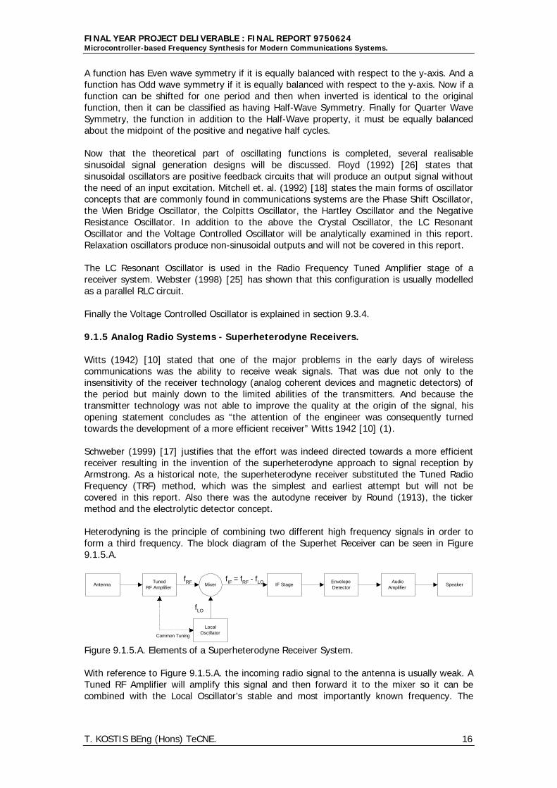
Heterodyning is the principle of combining two different high frequency signals in order toform a third frequency. The block diagram of the Superhet Receiver can be seen in Figure9.1.5.A.
AntennaTuned
RF Amplifier
LocalOscillator
IF StageEnvelopeDetector
AudioAmplifier
SpeakerfRF
fLO
fIF = fRF - fLOMixer
Common Tuning
Figure 9.1.5.A. Elements of a Superheterodyne Receiver System.
With reference to Figure 9.1.5.A. the incoming radio signal to the antenna is usually weak. ATuned RF Amplifier will amplify this signal and then forward it to the mixer so it can becombined with the Local Oscillator’s stable and most importantly known frequency. The
FINAL YEAR PROJECT DELIVERABLE : FINAL REPORT 9750624Microcontroller-based Frequency Synthesis for Modern Communications Systems.
T. KOSTIS BEng (Hons) TeCNE. 17
quality of the RF Amplifier dictates the sensitivity of the receiver, which is the minimum inputRF signal required to produce the audio signal at the output.
A Voltage Controlled Oscillator (VCO) can be used as the Local Oscillator in order to providean analog method of tuning the frequency range.
The mixer is a non-linear device that shifts the received signal at fRF to the IntermediateFrequency (IF) fIF. Essentially it produces the difference fRF-fLO and addition fRF+fLO
components as its output. The low frequency difference signal is called IntermediateFrequency fIF. The high frequency addition component is eliminated by filtering. Moreover theRF Amplifier and the LO signals are tuned together so the IF value always remains the same.(fLO=fRF-fIF)
The Intermediate Frequency Amplifier (IF AMP) provides most of the frequency selectivity,which is the extent to which a receiver can differentiate between the desired signal and othersignals.
The Detector incorporates an envelope amplitude variation detection circuit and generallyrecovers the original message signal from the modified IF input.
The Audio Amplifier increases the power level to a value suitable for driving the outputdevice (loudspeaker).
The Output Device converts the signal information back to its original form. Music andspeech are emanated in the air by the loudspeaker.In comparison, an AM receiver is very similar to an FM receiver. Both can besuperheterodyne types utilising the concept of the Intermediate Frequency (IF). Of coursethe difference is in the way the incoming signal is demodulated. Generally in AM theintelligence information is present in the carrier envelope fluctuations and therefore envelopelinearity must be maintained. And for FM, the intelligence information is present in thevariations of the instantaneous frequency and therefore these variations have to beconverted to amplitude variations by a device called a limiter. Usually the limiter function isincorporated in the detector block.
9.1.6. Analog Radio Systems - Phase Locked Loop Transmitters.
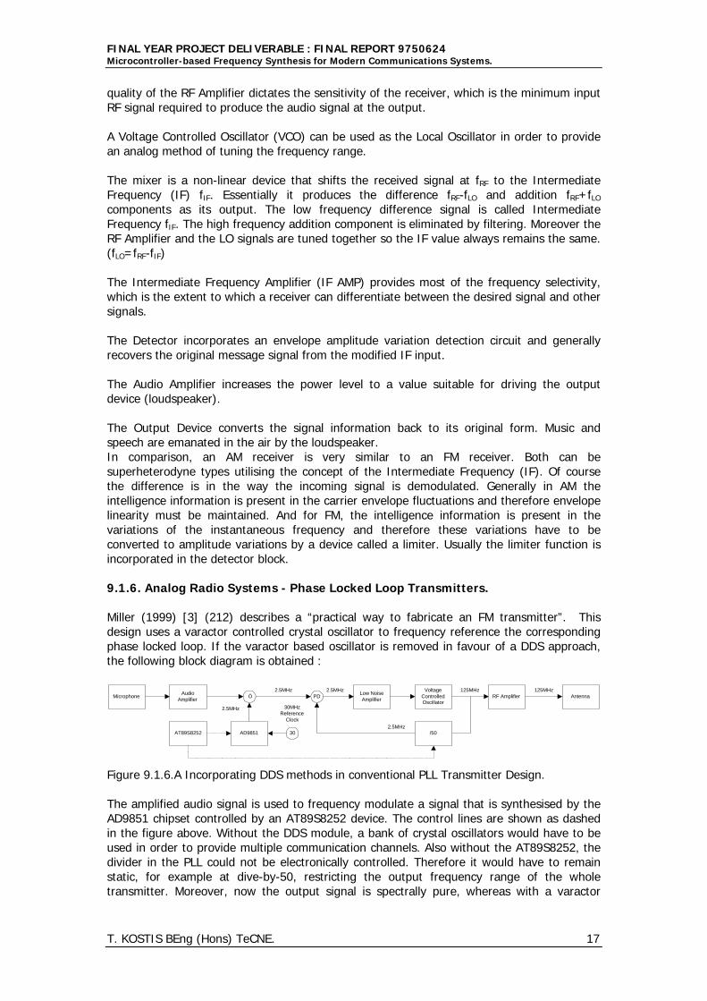
Miller (1999) [3] (212) describes a “practical way to fabricate an FM transmitter”. Thisdesign uses a varactor controlled crystal oscillator to frequency reference the correspondingphase locked loop. If the varactor based oscillator is removed in favour of a DDS approach,the following block diagram is obtained :
MicrophoneAudio
Amplifier
AD9851AT89S8252
30MHzReference
Clock
30
Ó PDLow NoiseAmplifier
VoltageControlledOscillator
/50
125MHzRF Amplifier Antenna
2.5MHz
2.5MHz
2.5MHz
125MHz2.5MHz
Figure 9.1.6.A Incorporating DDS methods in conventional PLL Transmitter Design.
The amplified audio signal is used to frequency modulate a signal that is synthesised by theAD9851 chipset controlled by an AT89S8252 device. The control lines are shown as dashedin the figure above. Without the DDS module, a bank of crystal oscillators would have to beused in order to provide multiple communication channels. Also without the AT89S8252, thedivider in the PLL could not be electronically controlled. Therefore it would have to remainstatic, for example at dive-by-50, restricting the output frequency range of the wholetransmitter. Moreover, now the output signal is spectrally pure, whereas with a varactor
FINAL YEAR PROJECT DELIVERABLE : FINAL REPORT 9750624Microcontroller-based Frequency Synthesis for Modern Communications Systems.
T. KOSTIS BEng (Hons) TeCNE. 18
oscillator there is a frequency drift of approximately +-200KHz. This would be due to thenon-linear characteristic of the variable capacitance of the varactor diode.
The PLL in this case provides a multiplication of 50 times the original reference signal makingpossible communications in the air-band (125MHz). It also provides the overall transmitterwith the required frequency stability. Any drift in the VCO centre frequency causes an inputto the Phase Detector that is slightly different from the expected exact 2.5MHz. The PhaseDetector output then develops an error signal that corrects the VCO centre frequency back tothe expected 125MHz. This dynamic equilibrium action of the Phase Detector with theVoltage Controlled Oscillator is the concept of the Phase Locked Loop.
9.2. Frequency Synthesis
A Frequency Synthesiser is a system that will generate any desired frequency from a singlecrystal source. The output frequency is dependent upon the unique characteristics of theelements of the frequency synthesiser, like the crystal resonance range.
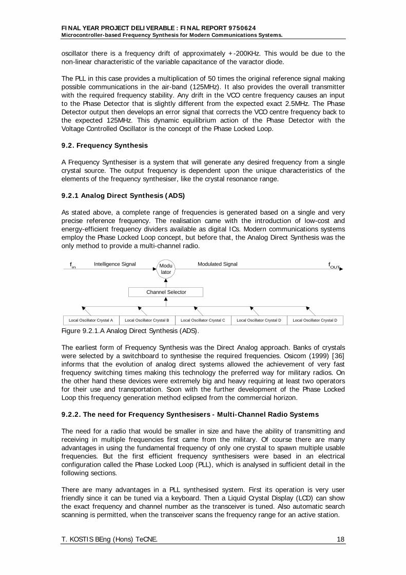
9.2.1 Analog Direct Synthesis (ADS)
As stated above, a complete range of frequencies is generated based on a single and veryprecise reference frequency. The realisation came with the introduction of low-cost andenergy-efficient frequency dividers available as digital ICs. Modern communications systemsemploy the Phase Locked Loop concept, but before that, the Analog Direct Synthesis was theonly method to provide a multi-channel radio.
Modulator
Intelligence Signal
Local Oscillator Crystal C
Modulated Signal
Local Oscillator Crystal BLocal Oscillator Crystal A Local Oscillator Crystal D Local Oscillator Crystal D
fOUTfin
Channel Selector
Figure 9.2.1.A Analog Direct Synthesis (ADS).
The earliest form of Frequency Synthesis was the Direct Analog approach. Banks of crystalswere selected by a switchboard to synthesise the required frequencies. Osicom (1999) [36]informs that the evolution of analog direct systems allowed the achievement of very fastfrequency switching times making this technology the preferred way for military radios. Onthe other hand these devices were extremely big and heavy requiring at least two operatorsfor their use and transportation. Soon with the further development of the Phase LockedLoop this frequency generation method eclipsed from the commercial horizon.
9.2.2. The need for Frequency Synthesisers - Multi-Channel Radio Systems
The need for a radio that would be smaller in size and have the ability of transmitting andreceiving in multiple frequencies first came from the military. Of course there are manyadvantages in using the fundamental frequency of only one crystal to spawn multiple usablefrequencies. But the first efficient frequency synthesisers were based in an electricalconfiguration called the Phase Locked Loop (PLL), which is analysed in sufficient detail in thefollowing sections.
There are many advantages in a PLL synthesised system. First its operation is very userfriendly since it can be tuned via a keyboard. Then a Liquid Crystal Display (LCD) can showthe exact frequency and channel number as the transceiver is tuned. Also automatic searchscanning is permitted, when the transceiver scans the frequency range for an active station.
FINAL YEAR PROJECT DELIVERABLE : FINAL REPORT 9750624Microcontroller-based Frequency Synthesis for Modern Communications Systems.
T. KOSTIS BEng (Hons) TeCNE. 19
The key to tuning a receiver to a desired frequency is precise control of the Local Oscillator(LO) signal, which is mixed with the Incoming Signal (IS) to produce the desiredIntermediate Frequency (IF). The Synthesiser output is used as the LO signal.
9.3. Phase Locked Loop (PLL)
The Phase Locked Loop (PLL) is a frequency selective negative feedback system which cansynchronise with an appropriate input signal and faithfully track all frequency and thereforeall phase changes associated with it.
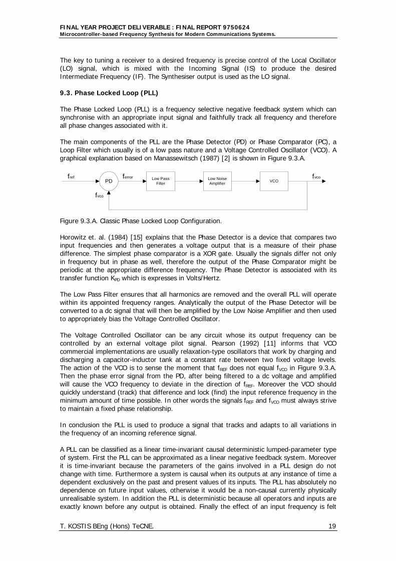
The main components of the PLL are the Phase Detector (PD) or Phase Comparator (PC), aLoop Filter which usually is of a low pass nature and a Voltage Controlled Oscillator (VCO). Agraphical explanation based on Manassewitsch (1987) [2] is shown in Figure 9.3.A.
PD Low PassFilter
ferrorVCO
fref fvco
fvco
Low NoiseAmplifier
Figure 9.3.A. Classic Phase Locked Loop Configuration.
Horowitz et. al. (1984) [15] explains that the Phase Detector is a device that compares twoinput frequencies and then generates a voltage output that is a measure of their phasedifference. The simplest phase comparator is a XOR gate. Usually the signals differ not onlyin frequency but in phase as well, therefore the output of the Phase Comparator might beperiodic at the appropriate difference frequency. The Phase Detector is associated with itstransfer function KPD which is expresses in Volts/Hertz.
The Low Pass Filter ensures that all harmonics are removed and the overall PLL will operatewithin its appointed frequency ranges. Analytically the output of the Phase Detector will beconverted to a dc signal that will then be amplified by the Low Noise Amplifier and then usedto appropriately bias the Voltage Controlled Oscillator.
The Voltage Controlled Oscillator can be any circuit whose its output frequency can becontrolled by an external voltage pilot signal. Pearson (1992) [11] informs that VCOcommercial implementations are usually relaxation-type oscillators that work by charging anddischarging a capacitor-inductor tank at a constant rate between two fixed voltage levels.The action of the VCO is to sense the moment that fREF does not equal fVCO in Figure 9.3.A.Then the phase error signal from the PD, after being filtered to a dc voltage and amplifiedwill cause the VCO frequency to deviate in the direction of fREF. Moreover the VCO shouldquickly understand (track) that difference and lock (find) the input reference frequency in theminimum amount of time possible. In other words the signals fREF and fVCO must always striveto maintain a fixed phase relationship.
In conclusion the PLL is used to produce a signal that tracks and adapts to all variations inthe frequency of an incoming reference signal.
A PLL can be classified as a linear time-invariant causal deterministic lumped-parameter typeof system. First the PLL can be approximated as a linear negative feedback system. Moreoverit is time-invariant because the parameters of the gains involved in a PLL design do notchange with time. Furthermore a system is causal when its outputs at any instance of time adependent exclusively on the past and present values of its inputs. The PLL has absolutely nodependence on future input values, otherwise it would be a non-causal currently physicallyunrealisable system. In addition the PLL is deterministic because all operators and inputs areexactly known before any output is obtained. Finally the effect of an input frequency is felt
FINAL YEAR PROJECT DELIVERABLE : FINAL REPORT 9750624Microcontroller-based Frequency Synthesis for Modern Communications Systems.
T. KOSTIS BEng (Hons) TeCNE. 20
throughout the system at the same time for all components classifying the PLL as a lumped-parameter model.
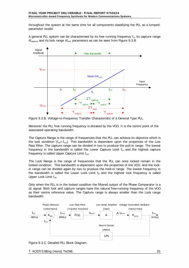
A general PLL system can be characterised by its free running frequency fo, its capture rangeÄfcapture and its lock range Äflock parameters as can be seen from Figure 9.3.B.
Verror
-Verror
fo
Slope=1/KVCO
2˜f capture
2˜f lock
Filter Bandwidth
InputFrequency
˜f hold-in ˜f hold-in
˜f pull-in ˜f pull-in
flll fullflcl fucl
SignalAmplitude
Figure 9.3.B. Voltage-to-Frequency Transfer Characteristic of a General Type PLL.
Moreover the PLL free running frequency is dictated by the VCO. It is the centre point of theassociated operating bandwidth.
The Capture Range is the range of frequencies that the PLL can achieve its objective which isthe lock condition (fref=fvco). This bandwidth is dependent upon the properties of the LowPass Filter. The capture range can be divided in two to produce the pull-in range. The lowestfrequency in the bandwidth is called the Lower Capture Limit flcl and the highest capturefrequency is called Upper Capture Limit fucl.
The Lock Range is the range of frequencies that the PLL can once locked remain in thelocked condition. This bandwidth is dependent upon the properties of the VCO. And the lock-in range can be divided again by two to produce the hold-in range. The lowest frequency inthe bandwidth is called the Lower Lock Limit flll and the highest lock frequency is calledUpper Lock Limit full.
Only when the PLL is in the locked condition the filtered output of the Phase Comparator is adc signal. Both lock and capture ranges have the natural free-running frequency of the VCOas their centre reference value. The Capture range is always smaller than the Lock rangebandwidth.
KPD F(s)ferror
KVCO
fref fvco
fvco
A
Phase Detector Low Pass Filter Low Noise Amplifier Voltage Controlled Oscillator
1/N
Mod-N Divider
REF(s) VCO(s)ERR(s)
Verror A Verror
[Volts/Hertz] [Hertz/Volts][Gain][Transfer Function]
[Ratio]
Figure 9.3.C. Detailed PLL Block Diagram.
FINAL YEAR PROJECT DELIVERABLE : FINAL REPORT 9750624Microcontroller-based Frequency Synthesis for Modern Communications Systems.
T. KOSTIS BEng (Hons) TeCNE. 21
After the above discussion Figure 9.3.A can be upgraded to include all the details that areassociated with a PLL system, as can be seen in Figure 9.3.C.
9.3.1. Analog Phase Locked Loop (APLL) and FM-PM Modulation-Demodulation
Analog Phase Locked Loops can be divided into two major categories according to thetransfer function of the loop filter. Therefore a PLL is considered to be of the First Order ifthe transfer function of the filter is 1. And it is classified as a Second Order when the filterexhibits a phase-lag behaviour, like the one shown in Equation 9.3.1.
F(s)= 1+l s1+r s (9.3.1)
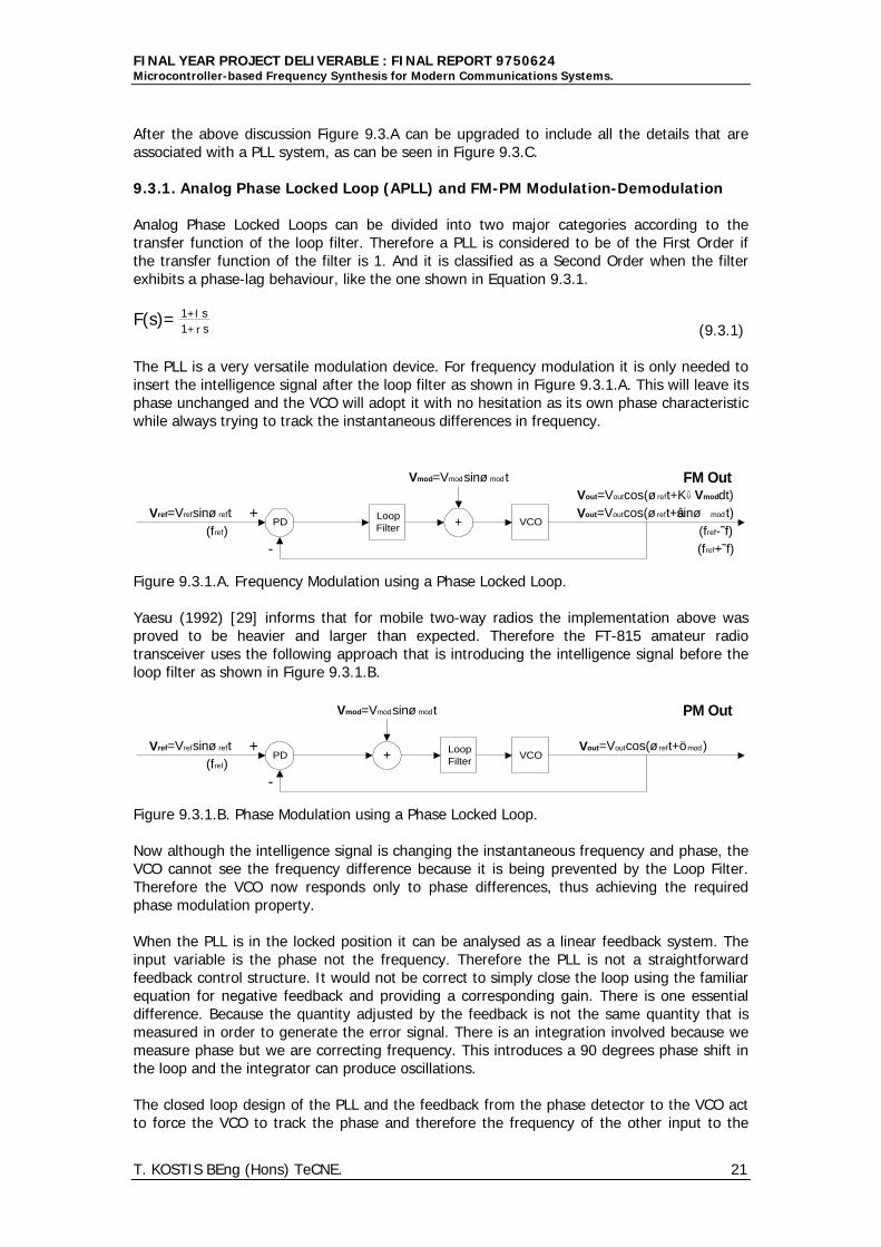
The PLL is a very versatile modulation device. For frequency modulation it is only needed toinsert the intelligence signal after the loop filter as shown in Figure 9.3.1.A. This will leave itsphase unchanged and the VCO will adopt it with no hesitation as its own phase characteristicwhile always trying to track the instantaneous differences in frequency.
PDLoopFilter
VCOVref=Vrefsinø reft
-
++
Vmod=Vmodsinø mod t
(fref)(fref+˜f)(fref-˜f)
FM OutVout=Voutcos(ø reft+Kò Vmoddt)Vout=Voutcos(ø reft+âsinø mod t)
Figure 9.3.1.A. Frequency Modulation using a Phase Locked Loop.
Yaesu (1992) [29] informs that for mobile two-way radios the implementation above wasproved to be heavier and larger than expected. Therefore the FT-815 amateur radiotransceiver uses the following approach that is introducing the intelligence signal before theloop filter as shown in Figure 9.3.1.B.
PDLoopFilter
VCOVref=Vrefsinø reft
-
++
Vmod=Vmodsinø modt PM Out
Vout=Voutcos(ø reft+ö mod)(fref)
Figure 9.3.1.B. Phase Modulation using a Phase Locked Loop.
Now although the intelligence signal is changing the instantaneous frequency and phase, theVCO cannot see the frequency difference because it is being prevented by the Loop Filter.Therefore the VCO now responds only to phase differences, thus achieving the requiredphase modulation property.
When the PLL is in the locked position it can be analysed as a linear feedback system. Theinput variable is the phase not the frequency. Therefore the PLL is not a straightforwardfeedback control structure. It would not be correct to simply close the loop using the familiarequation for negative feedback and providing a corresponding gain. There is one essentialdifference. Because the quantity adjusted by the feedback is not the same quantity that ismeasured in order to generate the error signal. There is an integration involved because wemeasure phase but we are correcting frequency. This introduces a 90 degrees phase shift inthe loop and the integrator can produce oscillations.
The closed loop design of the PLL and the feedback from the phase detector to the VCO actto force the VCO to track the phase and therefore the frequency of the other input to the

FINAL YEAR PROJECT DELIVERABLE : FINAL REPORT 9750624Microcontroller-based Frequency Synthesis for Modern Communications Systems.
T. KOSTIS BEng (Hons) TeCNE. 22
phase detector. If the external input of the PLL is a precise reference signal, the VCO willhave the same frequency as the PLL locks onto the reference input. The VCO output is usedas the LO signal.
LPFLow Pass Filter
VCOVoltage Controlled Oscillator
PCfOUT
fvco
fref
PhaseComparator
fFM-OUT
Figure 9.3.1.C. Demodulation using an Analog Phase Locked Loop (APLL).
The block diagram of a general analog phase locked loop used for demodulation can be seenat Figure 9.3.1.C. It is the error voltage signal that tries to force the VCO to follow the input,thus this being the demodulated FM output.
9.3.2. Digital Phase Locked Loop (DPLL) and Digital mod-N Divider Design
A modulo-N counter can be inserted between the VCO output and the Phase Detector Input.This method will generate a multiple of the input frequency fIN as shown in Figure 9.3.2.A.This is the basic technique for Digital Divider Frequency Synthesisers, which are also calledDigital Phase Locked Loop Synthesisers. The main disadvantage is that it is very difficult toimplement a divider for frequencies approximately of 100MHz and above.
/N DividerControl Panel
LPFLow Pass Filter
VCOVoltage Controlled Oscillator
PCfOUT
fvco
fref
PhaseComparator
fFM-OUT
Figure 9.3.2.A. Digital Phase Locked Loop (DPLL).
The solution to this limitation is to use a fixed value counter M after the VCO and before themain programmable divider. This method is called prescaling as shown in Figure 9.3.2.B. andits major disadvantage is that the frequency step size is increased in parallel by the samecount factor.
/N DividerProgrammable
LPFLow Pass Filter
VCOVoltage Controlled Oscillator
PCfOUT
fvco
fref
Phase Comparator
/M DividerFixed Prescaler
Figure 9.3.2.B. The Prescaling Function.
This may deem the whole design inappropriate for the application because the channelspacing may be too wide. One way to barely get around this problem is to reduce thereference frequency by this same amount of count A because low frequency oscillators areinefficient and the division ratio may now be asking for a very low reference frequency. Blakealso informs that neither programmable dividers are available at frequencies above 100 MHzmaking the construction of UHF synthesisers impossible with the previous method. But thereis a way to create steps in the output frequency that are almost independent of the referenceoscillator called Dual Modulus Prescaling.
FINAL YEAR PROJECT DELIVERABLE : FINAL REPORT 9750624Microcontroller-based Frequency Synthesis for Modern Communications Systems.
T. KOSTIS BEng (Hons) TeCNE. 23
The Dual Modulus Prescaler is a more flexible divider subsystem that can be programmed todivide by two consecutive integers. The main idea is to provide all the benefits of prescalingwhile at the same time maintaining the same frequency step size that would have beenobtained without even introducing any more dividers to the reference frequency.
9.3.3. Time and Frequency Domains
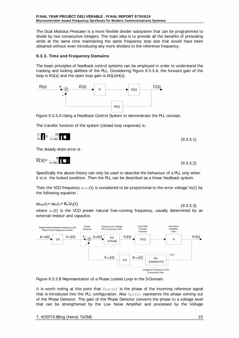
The basic principles of feedback control systems can be employed in order to understand thetracking and locking abilities of the PLL. Considering Figure 9.3.3.A, the forward gain of theloop is KG(s) and the open loop gain is KG(s)H(s).
KE(s)
G(s)
H(s)
R(s) C(s)
-
+Ó
Figure 9.3.3.A Using a Feedback Control System to demonstrate the PLL concept.
The transfer function of the system (closed loop response) is :
CHsLRHsL= KGHsL
1+KGHsL HHsL (9.3.3.1)
The steady-state error is :
E(s)= RHsL1+KGHsL H HsL (9.3.3.2)
Specifically the above theory can only be used to describe the behaviour of a PLL only whenit is in the locked condition. Then the PLL can be described as a linear feedback system.
Then the VCO frequency ùvco(t) is considered to be proportional to the error voltage Ve(t) bythe following equation :
wosc(t)=wo(t)+KoVe(t) (9.3.3.3)where ùo(t) is the VCO preset natural free-running frequency, usually determined by anexternal resistor and capacitor.
Kd[V/rad]
ö pd(s)F(s)
1/s
ö ref(s) Ve(s)
-
+Ó
Vd(s)A
Ko[rad/sec/V]
ø vco(s)
1/sø ref(s)
ö vco(s)
Loop FilterTransferFunction
Low NoiseAmplifier
Gain
VCO
PhaseDetector
Relationaship between Frequency andPhase in the Frequency Domain.
Voltage-to-Frequency VCOConversion Gain
Frequency-to-VoltagePD Conversion Gain
Figure 9.3.3.B Representation of a Phase Locked Loop in the S-Domain.
It is worth noting at this point that öref(s) is the phase of the incoming reference signalthat is introduced into the PLL configuration. Also öpd(s) represents the phase coming outof the Phase Detector. The gain of the Phase Detector converts the phase to a voltage levelthat can be strengthened by the Low Noise Amplifier and processed by the Voltage
FINAL YEAR PROJECT DELIVERABLE : FINAL REPORT 9750624Microcontroller-based Frequency Synthesis for Modern Communications Systems.
T. KOSTIS BEng (Hons) TeCNE. 24
Controlled Oscillator. Analytically the phase of the reference signal öref(s) and its dualöref(t) are connected to its corresponding frequency signal ùref(s) and its dualùref(t)in the Time Domain and in the Frequency domain with zero initial conditions asfollows :
w(t)= dfHtLdt
and f (t)=HfHtLLt=0+Ù0twHtL d t (9.3.3.4)
f (s)= 1s
w(s) (9.3.3.5)
9.3.4. Voltage Controlled Oscillators - Design and Stability Considerations
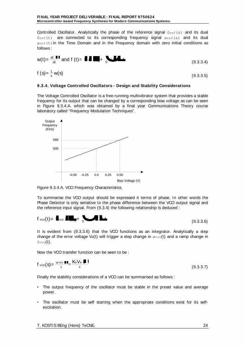
The Voltage Controlled Oscillator is a free-running multivibrator system that provides a stablefrequency for its output that can be changed by a corresponding bias voltage as can be seenin Figure 9.3.4.A. which was obtained by a final year Communications Theory courselaboratory called “Frequency Modulation Techniques”.
0.0 0.25 0.50-0.25-0.50
Bias Voltage (V)
OutputFrequency
(KHz)
500
588
Figure 9.3.4.A. VCO Frequency Characteristics.
To summarise the VCO output should be expressed it terms of phase. In other words thePhase Detector is only sensitive to the phase difference between the VCO output signal andthe reference input signal. From (9.3.4) the following relationship is deduced :
f vco(t)=Hf vcoHtLLt=0+Ù0twvcoHtL d t (9.3.3.6)
It is evident from (9.3.3.6) that the VCO functions as an integrator. Analytically a stepchange of the error voltage Ve(t) will trigger a step change in ùvco(t) and a ramp change inövco(t).
Now the VCO transfer function can be seen to be :
f vco(s)= w vcoHsLs
= KoVeHsLs (9.3.3.7)
Finally the stability considerations of a VCO can be summarised as follows :
• The output frequency of the oscillator must be stable in the preset value and averagepower.
• The oscillator must be self starting when the appropriate conditions exist for its self-
excitation.
FINAL YEAR PROJECT DELIVERABLE : FINAL REPORT 9750624Microcontroller-based Frequency Synthesis for Modern Communications Systems.
T. KOSTIS BEng (Hons) TeCNE. 25
• The oscillator must maintain the oscillations at the desired amplitude under all normalload conditions.
• The oscillator must produce a sinusoidal type of output and suppress all its associated
harmonics. Also it phase should be linear over the allocated bandwidth.
9.3.5. Phase Noise
Atmospheric noise and interference are not the only problems a communications receiverstation has to confront. Phase noise is spurious changes in the phase of a frequencysynthesiser’s output that produces energy at frequencies other than the intended ones.
Analytically the Intermediate frequency signal is proportional to the phase differencebetween the RF signal from the antenna and the local oscillator signal. Phase noise presentin the local oscillator contributes a linear-wise disturbance to the mixer’s output signal.Analytically this may be noise, interference, multipath fading, front-end noise or acombination of these. Of course the over the air multipath fading is outside the designer’scontrol, therefore it is of paramount importance to combat phase noise in the overall design.
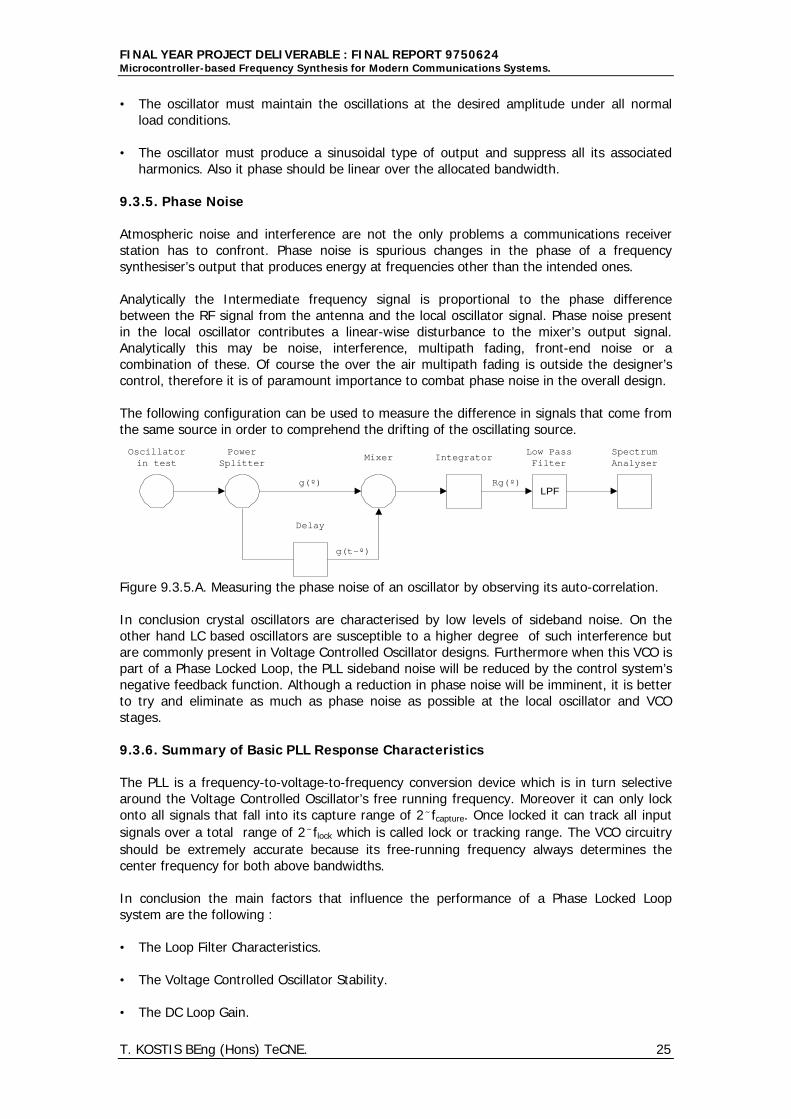
The following configuration can be used to measure the difference in signals that come fromthe same source in order to comprehend the drifting of the oscillating source.
g(t-ë)
PowerSplitter
Oscillatorin test
Mixer Integrator
LPFRg(ë)
Delay
g(ë)
Low PassFilter
SpectrumAnalyser
Figure 9.3.5.A. Measuring the phase noise of an oscillator by observing its auto-correlation.
In conclusion crystal oscillators are characterised by low levels of sideband noise. On theother hand LC based oscillators are susceptible to a higher degree of such interference butare commonly present in Voltage Controlled Oscillator designs. Furthermore when this VCO ispart of a Phase Locked Loop, the PLL sideband noise will be reduced by the control system’snegative feedback function. Although a reduction in phase noise will be imminent, it is betterto try and eliminate as much as phase noise as possible at the local oscillator and VCOstages.
9.3.6. Summary of Basic PLL Response Characteristics
The PLL is a frequency-to-voltage-to-frequency conversion device which is in turn selectivearound the Voltage Controlled Oscillator’s free running frequency. Moreover it can only lockonto all signals that fall into its capture range of 2Äfcapture. Once locked it can track all inputsignals over a total range of 2Äflock which is called lock or tracking range. The VCO circuitryshould be extremely accurate because its free-running frequency always determines thecenter frequency for both above bandwidths.
In conclusion the main factors that influence the performance of a Phase Locked Loopsystem are the following :
• The Loop Filter Characteristics. • The Voltage Controlled Oscillator Stability. • The DC Loop Gain.
FINAL YEAR PROJECT DELIVERABLE : FINAL REPORT 9750624Microcontroller-based Frequency Synthesis for Modern Communications Systems.
T. KOSTIS BEng (Hons) TeCNE. 26
9.4. Direct Digital Synthesis (DDS)
All other signal generator methods need to utilise a form of a physical oscillating part whereits output is suitably manipulated and controlled by the timing elements (capacitors andinductors) of the frequency synthesiser. Direct Digital Synthesis is unique because it isdigitally deterministic. There are no actual moving (oscillating) parts and the generatedsignal is made up from its sampled discrete definition. Also of all the classic signal generationtechniques only DDS truly digitally constructs the output signal from the Read Only Memorylook-up table.
9.4.1. Principles of Operation
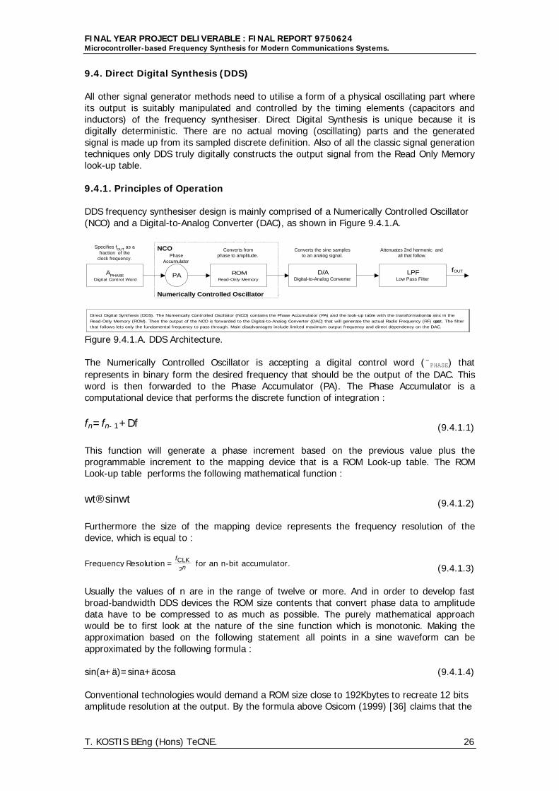
DDS frequency synthesiser design is mainly comprised of a Numerically Controlled Oscillator(NCO) and a Digital-to-Analog Converter (DAC), as shown in Figure 9.4.1.A.
NCO
Numerically Controlled Oscillator
Direct Digital Synthesis (DDS). The Numerically Controlled Oscillator (NCO) contains the Phase Accumulator (PA) and the look-up table with the transformation x to sinx in the
Read-Only Memory (ROM). Then the output of the NCO is forwarded to the Digital-to-Analog Converter (DAC) that will generate the actual Radio Frequency (RF) output. The filterthat follows lets only the fundamental frequency to pass through. Main disadvantages include limited maximum output frequency and direct dependency on the DAC.
LPFLow Pass Filter
D/ADigital-to-Analog Converter
ÄPHASEDigital Control Word
ROMRead-Only Memory
PA
PhaseAccumulator
Converts fromphase to amplitude.
Specifies fOUT as afraction of the
clock frequency.
Converts the sine samplesto an analog signal.
Attenuates 2nd harmonic andall that follow.
fOUT
Figure 9.4.1.A. DDS Architecture.
The Numerically Controlled Oscillator is accepting a digital control word (ÄPHASE) thatrepresents in binary form the desired frequency that should be the output of the DAC. Thisword is then forwarded to the Phase Accumulator (PA). The Phase Accumulator is acomputational device that performs the discrete function of integration :
fn=fn- 1+Df (9.4.1.1)
This function will generate a phase increment based on the previous value plus theprogrammable increment to the mapping device that is a ROM Look-up table. The ROMLook-up table performs the following mathematical function :
wt®sinwt (9.4.1.2)
Furthermore the size of the mapping device represents the frequency resolution of thedevice, which is equal to :
Frequency Resolution =fCLK2n for an n-bit accumulator. (9.4.1.3)
Usually the values of n are in the range of twelve or more. And in order to develop fastbroad-bandwidth DDS devices the ROM size contents that convert phase data to amplitudedata have to be compressed to as much as possible. The purely mathematical approachwould be to first look at the nature of the sine function which is monotonic. Making theapproximation based on the following statement all points in a sine waveform can beapproximated by the following formula :
sin(a+ä)=sina+äcosa (9.4.1.4)
Conventional technologies would demand a ROM size close to 192Kbytes to recreate 12 bitsamplitude resolution at the output. By the formula above Osicom (1999) [36] claims that the
FINAL YEAR PROJECT DELIVERABLE : FINAL REPORT 9750624Microcontroller-based Frequency Synthesis for Modern Communications Systems.
T. KOSTIS BEng (Hons) TeCNE. 27
size can be scaled down to 3kbytes which a considerable reduction in size and enhancementin speed.
The NCO is the information source to the DAC so that an RF output can be generated. Andthe phase to amplitude transformation is performed by the ROM Look-up table. The finaloutput of the Digital-to-Analog Converter (DAC) is realistically limited around 40% to 45% ofthe clock frequency fCLK. The maximum clock speeds achieved with a DDS are near the rangeof 1GHz, resulting in a bandwidth usage of 450MHz. Moreover the formula that is used toprogram the frequency is as follows :
fOUT =DPHASE fCLK
2n (9.4.1.5)
DDS technology allows the use of undersampling in order to eliminate the mixer andmodulator parts from future commercial radio designs. A brief explanation of the theory ofsampling and aliasing follows in the next section.
9.4.2. Sampling of Sinusoidal Signals and Aliasing
In many feature films a strange effect is directly noticeable. The wheels of a car seem to bemoving backwards although the car is definitely screaming down the highway at full speed.An indication to the cause of this effect may be the fact that the same effect is evident in allwestern movies, where the wheels of the stagecoach again seem to be moving backwards. Amovie is a collection of images that are brought together to form a film. Each imagerepresents one particular sample of the whole. Therefore movies have to abide by theNyquist criterion. So maybe the rate of sampling is of paramount importance to thisinvestigation. Considering the following analog sinusoidal signal :
x(t)=Asin(Wot+F )=Asin(2pFot+F ), periodic w ith To= 2 p
Wo.
(9.4.2.1)
The sampling rate used is designated as :
Fs = 1
Ts (9.4.2.2)
Tavsanoglu (1999) [23] has shown that the original analog signal is depicted as follows inthe digital domain :
x(nT s )=x(n)=Asin(WonT s +F )=Asin(2pF oF s
n+F ) (9.4.2.3)
wo=WoT s =WoF s
=2pF oF s (9.4.2.4)
fo=FoT s =F oF s (9.4.2.5)
Aliasing happens because :
x(n)=Asin(2p FoFs
n+F )=Asin(2p F oF s
n+2pkn+F )=Asin(2p Fo +kFs
Fsn+F )
(9.4.2.6)
Because the sampling of x(n) is periodic in frequency with a period of :
ws =2p Fs
Fs=2p
(9.4.2.7)
FINAL YEAR PROJECT DELIVERABLE : FINAL REPORT 9750624Microcontroller-based Frequency Synthesis for Modern Communications Systems.
T. KOSTIS BEng (Hons) TeCNE. 28
And it can be written as the following final expression :
x(n)=Asin((wo +2pk)n+F ), -p£wo £p. (9.4.2.8)
The conclusion of this section is that the period of the digital domain is a necessary andsufficient condition for all the information about the discrete time signal to be reconstructed.
9.4.3. Advantages and Disadvantages of Direct Digital Frequency Synthesisers
The main advantages of DDS systems are fine step resolution, low phase noise, transient-free (phase continuous) frequency changes, extraordinary flexibility as a modulator, smallform factor and very fast switching (typically less than a microsecond) which is important inspread-spectrum or frequency-hopping systems, including commercial spectroscopy andautomatic test equipment (ATE) systems. There is no other frequency synthesising systemthat can change frequencies as rapidly as a Direct Digital Frequency Synthesiser.
Though there are many variations, the conventional DDS architecture can be viewed as asimple assembly comprised of only three active components: the phase accumulator, amapping device, and a digital-to-analog converter.
The above list provides persuasive arguments for using DDS in most transceiver designs,since such qualities are difficult or expensive to achieve with alternative direct and indirectsynthesis methods. But there are disadvantages also, of which two impose seriousrestrictions upon the systems designer. First the DDS covers an operating range limited bythe sampling theory first introduced by Shannon and Nyquist. Proakis (1995) [14] explainsthat Shannon observed that that the average number of bits per symbol required to encodethe output of a Discrete Memoryless Source with arbitrarily small probability of decodingfailure is lower bounded by the source entropy which is the average self-information persource letter and is denoted by H(X). And the sampling theorem by Nyquist states that for adeterministic band-limited signal where f is the highest frequency present in the signal can befully represented by sampling it at a rate of equal or greater than 2f samples per second.Proakis (1995) [14] recalls that Nyquist arrived at this conclusion while working on theproblem of determining the maximum signalling rate that can be used over a telegraphchannel of a certain bandwidth without intersymbol interference. Practically the output of aDDS device is limited to about 45% of the maximum clock rate at which it can be operated.The broadest bandwidth DDS yet achieved has been clocked at somewhat over 1GHz, withan output bandwidth of about 450MHz.
The second limitation is spectral purity, which is governed by the density and complexity ofthe logic circuitry that is attainable at the desired operating speed. Spectral purity andoperating bandwidth are inversely correlated, as will be shown. Despite these limitations theDDS has evolved into an important tool and some of its functional capabilities are notattainable with any other signal generation technique.
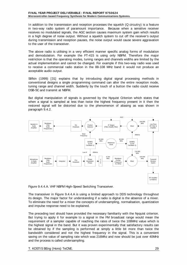
9.4.4. DDS-based Half-Duplex Radio Communications
A transceiver is simply a transmitter and a receiver in a single enclosure sharing somecommon parts. Usually the receiver bandwidth is the same or larger than the transmittercounterpart. For example a 2cm amateur radio transceiver like the Yaesu FT-415 can onlytransmit in the 144-146MHz but can receive a much wider collection of frequencies spanningthe whole VHF range. Of course the above restriction can be easily overridden bydisconnecting a limiting resistor and thus opening the band to transmit at all stations thereceiver can receive, provided the necessary license is obtained from the appropriate nationalauthorities.
FINAL YEAR PROJECT DELIVERABLE : FINAL REPORT 9750624Microcontroller-based Frequency Synthesis for Modern Communications Systems.
T. KOSTIS BEng (Hons) TeCNE. 29
In addition to the transmission and reception processes the squelch (Q circuitry) is a featurein two-way radio system of paramount importance. Because when a sensitive receiverreceives no modulated signals, the AGC section causes maximum system gain which resultsin a high degree of noise output. Without a squelch system to cut off the receiver’s outputduring transmission and reception pauses, the noise output would cause severe aggravationto the user of the transceiver.
The above radio is utilising in a very efficient manner specific analog forms of modulationand demodulation. For example the FT-415 is using only NBFM. Therefore the majorrestriction is that the operating modes, tuning ranges and channels widths are limited by theactual implementation and cannot be changed. For example if this two-way radio was usedto receive a commercial radio station in the 88-108 MHz band it would not produce anacceptable audio output.
Slifkin (1999) [31] explains that by introducing digital signal processing methods inconventional designs a single programming command can alter the entire reception mode,tuning range and channel width. Suddenly by the touch of a button the radio could receiveDSB-SC and transmit at NBFM.
But digital manipulation of signals is governed by the Nyquist Criterion which states thatwhen a signal is sampled at less than twice the highest frequency present in it then therestored signal will be distorted due to the phenomenon of aliasing as was shown inparagraph 9.4.2.
Microphone& AudioAmplifier
BandpassFilterAudio
Frequencies
IntegratorPre-
Emphasis
PhaseModulation
Phase
x20
Bandpass(Center
Frequency9.1 MHz)
RF Amplifier& Antenna
Mixer
AD9851(Local
Oscillator 2)
AD9851(Local
Oscillator 1)
144.000MHz
455KHzLow IF
ReferenceClock
30.000MHz
30.000MHz
9.100MHz
134.900MHz
Transmit/ReceiveSwitch
Low PassRF Filter &Amplifier
IF Stages(Filter-Amplify-Filter)
MixerProductDetector
BandpassFilterAudio
Frequencies
Speaker &Audio
Amplifier
De-Emphasis
144.000MHz
455KHzBeatFrequency
AGC
Figure 9.4.4.A. VHF NBFM High-Speed Switching Transceiver.
The transceiver in Figure 9.4.4.A is using a limited approach to DDS technology throughoutits design. The major factor for understanding if a radio is digital is the absence of a mixer.To eliminate the need for a mixer the concepts of undersampling, normalisation, quantizationand impulse response need to be explained.
The preceding text should have provided the necessary familiarity with the Nyquist criterion.But trying to apply it for example to a signal in the FM broadcast range would mean therequirement of a sampler capable of reaching the rates of twice the 108MHz value which isthe highest signal in the band. But it was proven experimentally that satisfactory results canbe obtained by if the sampling is performed at simply a little bit more than twice thebandwidth considered and not the highest frequency in the signal. This is a convenientsaving on the value of sampling rate which was 216Mhz and now should be just over 40MHzand the process is called undersampling.
FINAL YEAR PROJECT DELIVERABLE : FINAL REPORT 9750624Microcontroller-based Frequency Synthesis for Modern Communications Systems.
T. KOSTIS BEng (Hons) TeCNE. 30
Equation 9.4.2.5 depicts the concept of normalisation that links the baseband frequency ofan analog signal to its digital domain representation. The meaning of this equation is that thesamples of an analog signal depend both on the baseband and the sampling frequency.
For example two different signals sampled at two different frequencies may give the samevalue as the input to the arithmetical processor. Such an example is shown in Table 9.4.4.A.
Analog Frequency F0 Sampling Frequency Fs Ratio serving as input to a Processor.1KHz 100KHz 0.012KHz 200KHz 0.01
Table 9.4.4.A. Normalisation.
Sampling is performed with an Analog-to-Digital Converter. Since an 8-bit ADC can onlyprovide the limited range of two hundred and fifty six valid values, all incoming signals haveto be interpreted within that region. In the case that a signal falls between two adjacentvalues the ADC reports to its output the nearest value that it can determine. Therefore inmany cases the value reported by the ADC does not really match the actual amplitude valueof the original signal and this deviation is called the Quantization Error. Moreover this errorcan be described as a stochastic process or a deterministic formula should there be aharmonic relationship between the sampling rate and the reference signal.
A measure of performance for a DSP algorithm is its impulse response which is the outputsequence that is produced when the introduced input is the unit-impulse-sequence ä(n).When the output is non-zero for all n>0 then the system is characterised as an InfiniteImpulse Response type. On the other hand if the output returns to zero for all future valuesof n then the system is classified as a Finite Impulse Response type. Such DSP algorithmsare usually employed to replace the analog filters shown in Figure 9.4.4.A.
9.4.5. The Concept of Mixer Elimination
Communications systems must perform some sort of modulation which is the deliberatedeformation of a carrier signal by the impressed intelligence information in a manner that canallow the necessary and sufficient condition for the successful retrieval of this information bythe process of demodulation. Any signal however complex can be fully defined by itsamplitude, frequency and phase. And the modulation process is acting upon one of theseproperties by introducing complex circuitry after a pure radio frequency source, like aresonating crystal.
The DDS process is an optimum modulator because it allows extensive mathematicalmanipulations while the signal is in the digital domain. For example equation 9.4.2.6 statedthat a signal at a frequency f1 will be entirely indistinguishable from a signal at a frequency f2should a lower rate that the value dictated by the Nyquist criterion is used for sampling. Thisis one application of aliasing that can be proved beneficial for the purposes of demodulation.Because the aliases of the received signal can be programmed to fall into the audio rangeand therefore successfully retrieve the incoming intelligence signal.
Mathematically that means that a signal which is outside the region of :
(k-1) Fs2
£F0£k Fs2 (9.4.5.1)
will be still mapped to the normalised frequency set and finally fold into the digital domaininternal -pbw
0bp. Altogether this can be shown as :
F=F0+kFsÞ F0=F-kFsÞ w0=w-2pk (9.4.5.2)
FINAL YEAR PROJECT DELIVERABLE : FINAL REPORT 9750624Microcontroller-based Frequency Synthesis for Modern Communications Systems.
T. KOSTIS BEng (Hons) TeCNE. 31
Therefore the main idea is that a signal that is received on its original modulation frequencyof fmod would have its corresponding aliases at the faud frequencies which fall into the audiblespectrum.
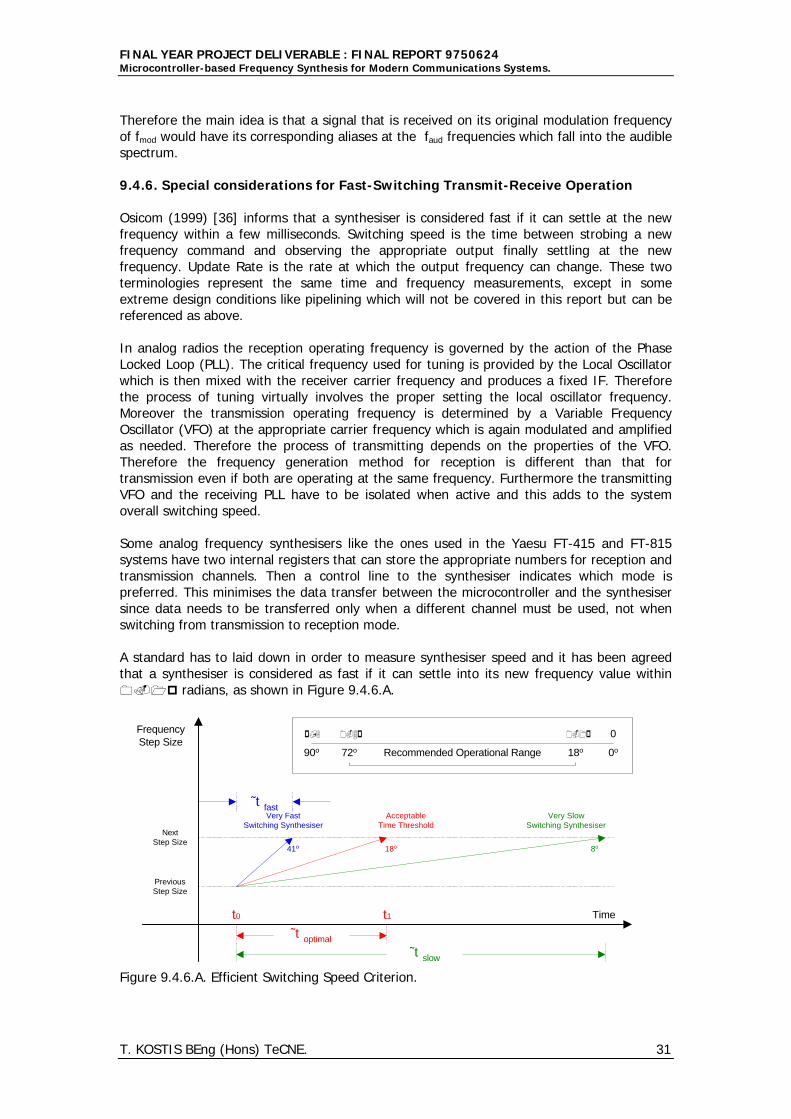
9.4.6. Special considerations for Fast-Switching Transmit-Receive Operation
Osicom (1999) [36] informs that a synthesiser is considered fast if it can settle at the newfrequency within a few milliseconds. Switching speed is the time between strobing a newfrequency command and observing the appropriate output finally settling at the newfrequency. Update Rate is the rate at which the output frequency can change. These twoterminologies represent the same time and frequency measurements, except in someextreme design conditions like pipelining which will not be covered in this report but can bereferenced as above.
In analog radios the reception operating frequency is governed by the action of the PhaseLocked Loop (PLL). The critical frequency used for tuning is provided by the Local Oscillatorwhich is then mixed with the receiver carrier frequency and produces a fixed IF. Thereforethe process of tuning virtually involves the proper setting the local oscillator frequency.Moreover the transmission operating frequency is determined by a Variable FrequencyOscillator (VFO) at the appropriate carrier frequency which is again modulated and amplifiedas needed. Therefore the process of transmitting depends on the properties of the VFO.Therefore the frequency generation method for reception is different than that fortransmission even if both are operating at the same frequency. Furthermore the transmittingVFO and the receiving PLL have to be isolated when active and this adds to the systemoverall switching speed.
Some analog frequency synthesisers like the ones used in the Yaesu FT-415 and FT-815systems have two internal registers that can store the appropriate numbers for reception andtransmission channels. Then a control line to the synthesiser indicates which mode ispreferred. This minimises the data transfer between the microcontroller and the synthesisersince data needs to be transferred only when a different channel must be used, not whenswitching from transmission to reception mode.
A standard has to laid down in order to measure synthesiser speed and it has been agreedthat a synthesiser is considered as fast if it can settle into its new frequency value within0.1p radians, as shown in Figure 9.4.6.A.
˜t optimal
t0 t1
FrequencyStep Size
Time
18o
PreviousStep Size
NextStep Size
˜t fast
41o
AcceptableTime Threshold
Very FastSwitching Synthesiser
0o90o 72o 18o
00.1p0.4pp/2
Recommended Operational Range
Very SlowSwitching Synthesiser
8o
˜t slow
Figure 9.4.6.A. Efficient Switching Speed Criterion.
FINAL YEAR PROJECT DELIVERABLE : FINAL REPORT 9750624Microcontroller-based Frequency Synthesis for Modern Communications Systems.
T. KOSTIS BEng (Hons) TeCNE. 32
A DDS based design would eliminate the need for a VFO and dedicated reception PLLbecause it is the fastest method of changing frequencies. The switching time can be as fastas the full bandwidth per one clock cycle plus the delay introduced by the output filter.Therefore the update rate can be as high as one gigahertz.
9.5. Comparison between Direct and Indirect Frequency Synthesiser Methods
Complete Direct Digital Frequency Synthesising (CDDFS) products exhibit evident advantagesover purely analog and digital phase locked loop designs for agile (accurate, rapidlyswitching with low distortion) frequency synthesis applications. The major advantages ofDDS systems over PLL-only designs are faster frequency switching time, finer tuning stepresolution, more generous operational bandwidth, lower phase noise, smaller form factor andpower dissipation requirements, lower manufacturing costs and overall implementationcomplexity.
The output frequency and phase of a DDS system can be precisely and rapidly manipulatedunder digital processor control. The change of frequencies can be as rapid as a rate of up to23 million output frequency changes per second. In contrast the analog PLL frequencyswitching time is a function of its feedback loop settling time and VCO response time which isusually greater than 1 msecs. DDS-based synthesiser switching time is limited only by DDSdigital processing delay. For example the minimum output frequency switching time of theAD9851 device is 43 nsecs.
Other inherent DDS attributes include the ability to tune with extremely fine frequency andphase step resolution. Coupled with a hybrid or fractional-N PLL design DDS technology isgradually advancing into higher bandwidth coverage. Specifically the AD9851 device has a32-bit phase accumulator which enables it to output frequency tuning resolutions much finerthan a PLL-based synthesiser. Moreover the AD9851 has a tuneable output resolution of 0.06Hz with a clock frequency of 30 MHz. Furthermore the output of these devices is phase-continuous during the transition to the new frequency. In contrast, the basic PLL-basedanalog synthesiser typically has an output tuning resolution of 1 kHz. Therefore it lacks theinherent resolution afforded by the digital signal processing.
The critical feedback loop bandwidth and input reference frequency relationship determinesthe stable employable frequency range of a typical analog PLL circuit. DDS-basedsynthesisers are immune to such loop filter stability issues and their tuneable range is equalto the current Nyquist range which is half the reference clock rate.
Because of the frequency division DDS-based solutions have a clear advantage over analogPLL synthesisers in output phase noise. Because the output phase noise of a DDS synthesiseris actually better than that of its reference clock source while analog PLL-based synthesisershave the disadvantage of actually multiplying the phase noise present in their frequencyreference.
The highly integrated AD9851 series DDS devices are packaged in very small surface-mountpackages requiring no more board space than most high-quality equivalent bandwidthdiscrete PLL synthesiser implementations.
The pricing for DDS-based solutions with an equivalent bandwidth to traditional PLL-basedsolutions has become extremely competitive for high-volume orders as can be seen from anycommercial publication like the Applied Microwave and Wireless (2000) [33].
Current DDS synthesisers dissipate much less power than even earlier discrete DDS solutions.For example, Analog Devices (1998) [34] claims that the AD9850 device dissipates 155 mWat 3.3 V when generating a 40-MHz signal with a 100 MHz reference clock. This is anextremely competitive power consumption with comparable analog and digital PLL-basedcircuits.
FINAL YEAR PROJECT DELIVERABLE : FINAL REPORT 9750624Microcontroller-based Frequency Synthesis for Modern Communications Systems.
T. KOSTIS BEng (Hons) TeCNE. 33
DDS solutions have reduced overall implementation complexity. First in most chips the DACis included on-die. This in turn is eliminating a great amount of RF design expertise requiredto connect a ROM chip to a D/A converter to achieve the same result. Moreover a simpledigital instruction set for control minimises the complexity of support hardware. Digitalsystem design replaces the analog-intensive system design required for PLL-based analogsynthesiser solutions to similar problems.
In conclusion the combination of the above characteristics makes the Direct Digital Synthesistechnology extremely popular in military and civil aviation radar and communicationssystems. In fact, DDS technology was previously relegated almost exclusively to high-endand military applications. For it was costly, required high power and was generally difficult toimplement. The main reason was that DDS requires a discrete high-speed signal DAC whichwas not either available or could not be incorporated in one chip like the case in the moderndevices. DDS-based designs have excellent AC performance, low power, low price and smallsize over their non-DDS implemented counterpart systems.
10. DESIGN & TECHNICAL APPROACH
The technical development of the FB14 project was closely monitored by the author and thesupervisor during several meetings which are evident in the project logbook. The list ofmeetings can be seen in appendix 15.8.
10.1. The Concept of the FB14 Project
This project will try to eliminate the need to use a Personal Computer to program an AD9851Direct Digital Frequency Synthesiser for demonstration purposes as outlined in the AD9851datasheet. Furthermore the project will try to experimentally prove that the AD9851 can beprogrammed by a completely digital bus and produce a purely analog sinusoidal frequency.This in turn will provide a design with less components because the two flip flops that areused in the original Analog Devices design can be eliminated. The reason is that they serveonly as buffers for a PC-compatible system’s parallel port and have absolutely no otherrelationship with the AD9851 device.
10.2. Principles of Operation
The AD9851 is a digitally programmable frequency synthesiser and clock generator. Byproviding an oscillator arrangement with a stable reference signal the AD9851 generates astable frequency and phase programmable digitised analog output sine wave. This sine wavecan be used directly as a frequency source for Local Oscillator purposes or can be internallyconverted into a square wave for clock generator applications. The high speed DDS coreneeds a 32bit Frequency Tuning Word (FTW). The Output Tuning Resolution (OTR) isestimated at 0.04Hz with a 180Mhz reference oscillator. This device was chosen for thisproject because it incorporates a 6xREFCLK multiplier that eliminates the need for a veryhigh speed reference oscillator. When engaged a reference frequency of 30Mhz will providethe necessary 180Mhz required.
Phase can be programmed in five increments of 11.25 degrees.
Word Data[7] Data[6] Data[5] Data[4] Data[3] Data[2] Data[1] Data[0]W0 Phase4 Phase3 Phase2 Phase1 Phase0 PWRDN Logic0 6x ON
Value 56.25o 45.00 o 33.75 o 22.50 o 11.25 o 0 or 1 0 0 or 1
Table 10.2.A. Explanation of the Phase Value Programming Word (W0).
The description of the rest four programming words are as follows :
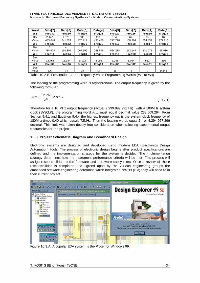
FINAL YEAR PROJECT DELIVERABLE : FINAL REPORT 9750624Microcontroller-based Frequency Synthesis for Modern Communications Systems.
T. KOSTIS BEng (Hons) TeCNE. 34
Word Data[7] Data[6] Data[5] Data[4] Data[3] Data[2] Data[1] Data[0]W1 Freq31 Freq30 Freq29 Freq28 Freq27 Freq26 Freq25 Freq24Dec
Value2.147.
483.6481.073.
741.824536.
870.912268.
435.456134.
217.72867.
108.86433.
554.43216.
777.216W2 Freq23 Freq22 Freq21 Freq20 Freq19 Freq18 Freq17 Freq16Dec
Value8.
388.6084.
194.3042.
097.1521.
048.576 524.288 262.144 131.072 65.536W3 Freq15 Freq14 Freq13 Freq12 Freq11 Freq10 Freq09 Freq08Dec
Value 32.768 16.384 8.192 4.096 2.048 1.024 512 256W4 Freq07 Freq06 Freq05 Freq04 Freq03 Freq02 Freq01 Freq00Dec
Value 128 64 32 16 8 4 2 0 or 1
Table 10.2.B. Explanation of the Frequency Value Programming Words (W1 to W4).
The loading of the programming word is asynchronous. The output frequency is given by thefollowing formula :
fOUT =˜ PHASE
232 SYSCLK
(10.2.1)
Therefore for a 10 MHz output frequency (actual 9.999.999,991 Hz), with a 180MHz systemclock (SYSCLK), the programming word ÄPHASE must equal decimal value 238.609.294. FromSection 9.4.1 and Equation 9.4.4 the highest frequency out is the system clock frequency of180Mhz times 0.40 which equals 72MHz. Then the loading words equal 232 or 4.294.967.296decimal. This limit was taken deeply into consideration when selecting experimental outputfrequencies for the project.
10.3. Project Schematic Diagram and Breadboard Design
Electronic systems are designed and developed using modern EDA (Electronics DesignAutomation) tools. The process of electronic design begins after product specifications aredefined and the implementation strategy for the system is decided. The implementationstrategy determines how the instrument performance criteria will be met. This process willassign responsibilities to the firmware and hardware subsystems. Once a review of theseresponsibilities is completed and agreed upon by the various engineering groups theembedded software engineering determine which integrated circuits (ICs) they will need to intheir current project.
Figure 10.3.A. A popular EDA system is the Protel for Windows 99.
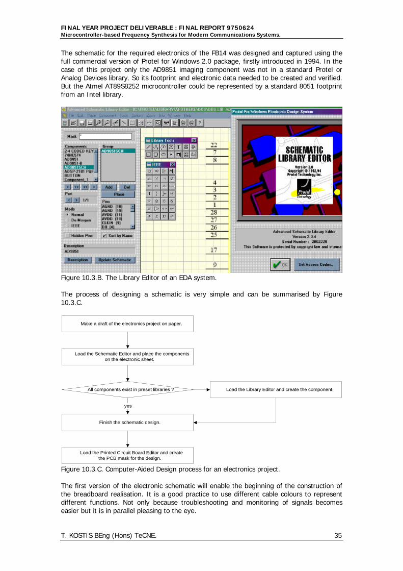
FINAL YEAR PROJECT DELIVERABLE : FINAL REPORT 9750624Microcontroller-based Frequency Synthesis for Modern Communications Systems.
T. KOSTIS BEng (Hons) TeCNE. 35
The schematic for the required electronics of the FB14 was designed and captured using thefull commercial version of Protel for Windows 2.0 package, firstly introduced in 1994. In thecase of this project only the AD9851 imaging component was not in a standard Protel orAnalog Devices library. So its footprint and electronic data needed to be created and verified.But the Atmel AT89S8252 microcontroller could be represented by a standard 8051 footprintfrom an Intel library.
Figure 10.3.B. The Library Editor of an EDA system.
The process of designing a schematic is very simple and can be summarised by Figure10.3.C.
Make a draft of the electronics project on paper.
Load the Schematic Editor and place the componentson the electronic sheet.
Finish the schematic design.
All components exist in preset libraries ?
yes
Load the Library Editor and create the component.
Load the Printed Circuit Board Editor and createthe PCB mask for the design.
Figure 10.3.C. Computer-Aided Design process for an electronics project.
The first version of the electronic schematic will enable the beginning of the construction ofthe breadboard realisation. It is a good practice to use different cable colours to representdifferent functions. Not only because troubleshooting and monitoring of signals becomeseasier but it is in parallel pleasing to the eye.
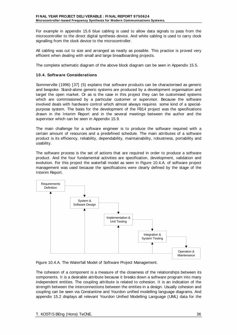
FINAL YEAR PROJECT DELIVERABLE : FINAL REPORT 9750624Microcontroller-based Frequency Synthesis for Modern Communications Systems.
T. KOSTIS BEng (Hons) TeCNE. 36
For example in appendix 15.6 blue cabling is used to allow data signals to pass from themicrocontroller to the direct digital synthesis device. And white cabling is used to carry clocksignalling from the clock device to the microcontroller.
All cabling was cut to size and arranged as neatly as possible. This practice is proved veryefficient when dealing with small and large breadboarding projects.
The complete schematic diagram of the above block diagram can be seen in Appendix 15.5.
10.4. Software Considerations
Sommerville (1996) [37] (5) explains that software products can be characterised as genericand bespoke. Stand-alone generic systems are produced by a development organisation andtarget the open market. Or as is the case in this project they can be customised systemswhich are commissioned by a particular customer or supervisor. Because the softwareinvolved deals with hardware control which almost always requires some kind of a special-purpose system. The basis for the development of the FB14 project was the specificationsdrawn in the Interim Report and in the several meetings between the author and thesupervisor which can be seen in Appendix 15.9.
The main challenge for a software engineer is to produce the software required with acertain amount of resources and a predefined schedule. The main attributes of a softwareproduct is its efficiency, reliability, dependability, maintainability, robustness, portability andusability.
The software process is the set of actions that are required in order to produce a softwareproduct. And the four fundamental activities are specification, development, validation andevolution. For this project the waterfall model as seen in Figure 10.4.A. of software projectmanagement was used because the specifications were clearly defined by the stage of theInterim Report.
RequirementsDefinition
System &Software Design
Implementation &Unit Testing
Integration &System Testing
Operation &Maintenance
Figure 10.4.A. The Waterfall Model of Software Project Management.
The cohesion of a component is a measure of the closeness of the relationships between itscomponents. It is a desirable attribute because it breaks down a software program into manyindependent entities. The coupling attribute is related to cohesion. It is an indication of thestrength between the interconnections between the entities in a design. Usually cohesion andcoupling can be seen via Constantine and Yourdon unified modelling language diagrams. Andappendix 15.2 displays all relevant Yourdon Unified Modelling Language (UML) data for the

FINAL YEAR PROJECT DELIVERABLE : FINAL REPORT 9750624Microcontroller-based Frequency Synthesis for Modern Communications Systems.
T. KOSTIS BEng (Hons) TeCNE. 37
FB14 Project. Moreover appendix 15.3 contains all relevant Data Dictionaries and reportsassociated with the UML approach to software engineering.
Finally the Atmel Microcontroller was programmed in Franklin C with 8051 extensions. Thefinal software version was developed using the Franklin software package. Appendix 15.4displays all relevant source code data.
10.5. Hardware Considerations
The development tool used for programming the AT89S8252 Microcontroller was the AtmelStarter Kit. It is a simple yet extremely efficient small board that can erase, program andverify the AVR AT90 and AT89 series of devices.
To make the AT89S8252 start executing its on-chip code, the EA pin must be held high. Thisis accomplished in the Atmel board by running a cable from pin 2 to pin 1 of Port E. ActuallyPort E on the board is a collection of control signals and not a specific input/output channellike the other four 8051 port compatible pin collections. There follows the exact configurationof cabling in order to program the AT89S8252 chip.
Serial 1
Serial 1
Power
1 2
3 4
5 6
R A
RESET ARESET
1 2
3 4
5 6
PORT E
ON/OFF
ìP
LEDS SWITCH
PORT C
PORT A
LEDS LEDS
PORT DPORT B
SWITCHES
LEDS
IBM Compatible
Zetagi HP SeriesStabilized Power Supply 5A
Figure 10.5.A. The connections on the Atmel Development Board.
Furthermore the method of connecting the parallel flat cable in order to test the output of aport is shown again if Figure 10.5.A. The flat cable has a red stripe indicating its continuityand orientation. If the red stripe is connected on the right side of the LEDS port then theother red stripe should be connected to PORT C as shown above. By this way the LEDS willlight in order of lower to higher making debugging easier.
The clocking circuitry that drives the AT89S8252 for this project is an EXO-3 programmableminiature crystal oscillator. Pin 1 is connected directly to pin (XTAL 1) of the AT89S8252 asdirected by the corresponding EXO datasheet from RS Components (1997) [35].
The circuitry is designed to reset on power-up eliminating the need for a separate resetswitch as directed by Intel (1993) [5]. Bezanov (1999) [24] has shown that the firmware of amicrocontroller can be utilised to provide an electrical signal which can be used as a resetwithout any buffering intermediary integrated components. And this signal is the first signalthat is conveyed to the DDS device in order to ensure its parallel initialisation.
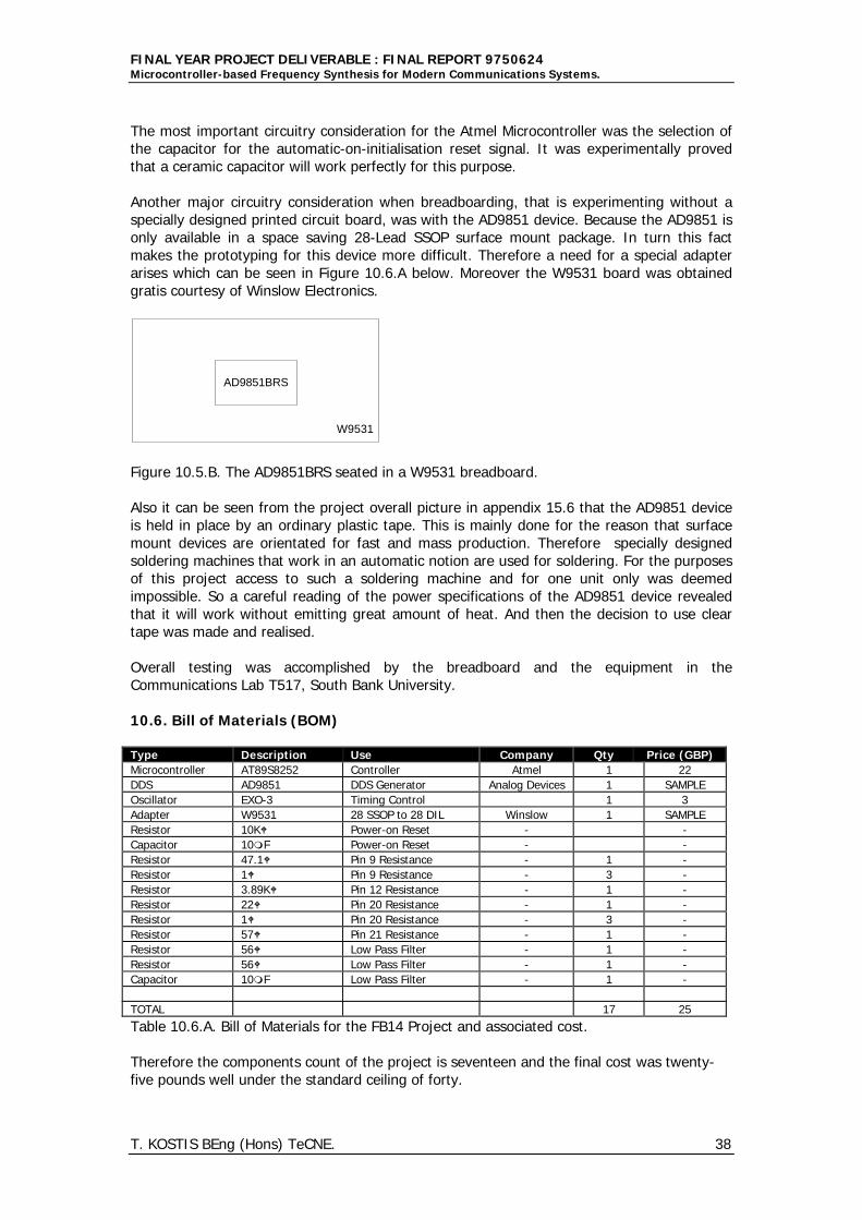
FINAL YEAR PROJECT DELIVERABLE : FINAL REPORT 9750624Microcontroller-based Frequency Synthesis for Modern Communications Systems.
T. KOSTIS BEng (Hons) TeCNE. 38
The most important circuitry consideration for the Atmel Microcontroller was the selection ofthe capacitor for the automatic-on-initialisation reset signal. It was experimentally provedthat a ceramic capacitor will work perfectly for this purpose.
Another major circuitry consideration when breadboarding, that is experimenting without aspecially designed printed circuit board, was with the AD9851 device. Because the AD9851 isonly available in a space saving 28-Lead SSOP surface mount package. In turn this factmakes the prototyping for this device more difficult. Therefore a need for a special adapterarises which can be seen in Figure 10.6.A below. Moreover the W9531 board was obtainedgratis courtesy of Winslow Electronics.
W9531
AD9851BRS
Figure 10.5.B. The AD9851BRS seated in a W9531 breadboard.
Also it can be seen from the project overall picture in appendix 15.6 that the AD9851 deviceis held in place by an ordinary plastic tape. This is mainly done for the reason that surfacemount devices are orientated for fast and mass production. Therefore specially designedsoldering machines that work in an automatic notion are used for soldering. For the purposesof this project access to such a soldering machine and for one unit only was deemedimpossible. So a careful reading of the power specifications of the AD9851 device revealedthat it will work without emitting great amount of heat. And then the decision to use cleartape was made and realised.
Overall testing was accomplished by the breadboard and the equipment in theCommunications Lab T517, South Bank University.
10.6. Bill of Materials (BOM)
Type Description Use Company Qty Price (GBP)Microcontroller AT89S8252 Controller Atmel 1 22DDS AD9851 DDS Generator Analog Devices 1 SAMPLEOscillator EXO-3 Timing Control 1 3Adapter W9531 28 SSOP to 28 DIL Winslow 1 SAMPLEResistor 10KW Power-on Reset - -Capacitor 10mF Power-on Reset - -Resistor 47.1W Pin 9 Resistance - 1 -Resistor 1W Pin 9 Resistance - 3 -Resistor 3.89KW Pin 12 Resistance - 1 -Resistor 22W Pin 20 Resistance - 1 -Resistor 1W Pin 20 Resistance - 3 -Resistor 57W Pin 21 Resistance - 1 -Resistor 56W Low Pass Filter - 1 -Resistor 56W Low Pass Filter - 1 -Capacitor 10mF Low Pass Filter - 1 -
TOTAL 17 25
Table 10.6.A. Bill of Materials for the FB14 Project and associated cost.
Therefore the components count of the project is seventeen and the final cost was twenty-five pounds well under the standard ceiling of forty.
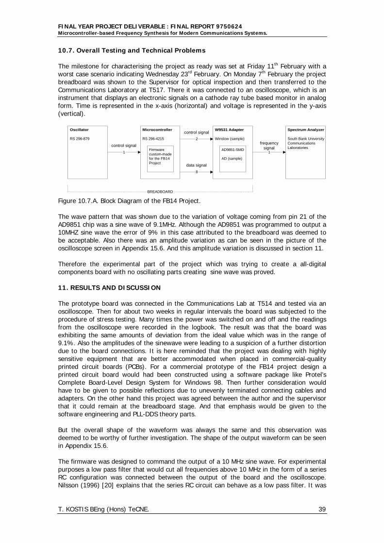
FINAL YEAR PROJECT DELIVERABLE : FINAL REPORT 9750624Microcontroller-based Frequency Synthesis for Modern Communications Systems.
T. KOSTIS BEng (Hons) TeCNE. 39
10.7. Overall Testing and Technical Problems
The milestone for characterising the project as ready was set at Friday 11th February with aworst case scenario indicating Wednesday 23rd February. On Monday 7th February the projectbreadboard was shown to the Supervisor for optical inspection and then transferred to theCommunications Laboratory at T517. There it was connected to an oscilloscope, which is aninstrument that displays an electronic signals on a cathode ray tube based monitor in analogform. Time is represented in the x-axis (horizontal) and voltage is represented in the y-axis(vertical).
Oscillator
RS 296-879
W9531 Adapter
Winslow (sample)
Microcontroller
RS 296-4215
AD9851-SMD
AD (sample)
1
2
8
1
control signal
control signal
data signal
frequencysignal
Spectrum Analyzer
South Bank UniversityCommunicationsLaboratories
BREADBOARD
Firmwarecustom-madefor the FB14Project
Figure 10.7.A. Block Diagram of the FB14 Project.
The wave pattern that was shown due to the variation of voltage coming from pin 21 of theAD9851 chip was a sine wave of 9.1MHz. Although the AD9851 was programmed to output a10MHZ sine wave the error of 9% in this case attributed to the breadboard was deemed tobe acceptable. Also there was an amplitude variation as can be seen in the picture of theoscilloscope screen in Appendix 15.6. And this amplitude variation is discussed in section 11.
Therefore the experimental part of the project which was trying to create a all-digitalcomponents board with no oscillating parts creating sine wave was proved.
11. RESULTS AND DISCUSSION
The prototype board was connected in the Communications Lab at T514 and tested via anoscilloscope. Then for about two weeks in regular intervals the board was subjected to theprocedure of stress testing. Many times the power was switched on and off and the readingsfrom the oscilloscope were recorded in the logbook. The result was that the board wasexhibiting the same amounts of deviation from the ideal value which was in the range of9.1%. Also the amplitudes of the sinewave were leading to a suspicion of a further distortiondue to the board connections. It is here reminded that the project was dealing with highlysensitive equipment that are better accommodated when placed in commercial-qualityprinted circuit boards (PCBs). For a commercial prototype of the FB14 project design aprinted circuit board would had been constructed using a software package like Protel’sComplete Board-Level Design System for Windows 98. Then further consideration wouldhave to be given to possible reflections due to unevenly terminated connecting cables andadapters. On the other hand this project was agreed between the author and the supervisorthat it could remain at the breadboard stage. And that emphasis would be given to thesoftware engineering and PLL-DDS theory parts.
But the overall shape of the waveform was always the same and this observation wasdeemed to be worthy of further investigation. The shape of the output waveform can be seenin Appendix 15.6.
The firmware was designed to command the output of a 10 MHz sine wave. For experimentalpurposes a low pass filter that would cut all frequencies above 10 MHz in the form of a seriesRC configuration was connected between the output of the board and the oscilloscope.Nilsson (1996) [20] explains that the series RC circuit can behave as a low pass filter. It was
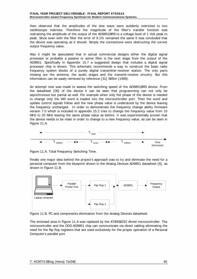
FINAL YEAR PROJECT DELIVERABLE : FINAL REPORT 9750624Microcontroller-based Frequency Synthesis for Modern Communications Systems.
T. KOSTIS BEng (Hons) TeCNE. 40
then observed that the amplitudes of the sine wave were suddenly restricted to twooscilloscope matrices. Therefore the magnitude of the filter’s transfer function wasrestraining the amplitude of the output of the AD9851BRS to a voltage level of 1 Volt peak topeak. Since even with the filter the error of 9.1% remained the same it was concluded thatthe device was operating as it should. Simply the connections were obstructing the correctoutput frequency value.
Also it might be speculated that in actual commercial designs either the digital signalprocessor or probably a passive or active filter is the next stage from the output of theAD9851. Specifically in Appendix 15.7 a suggested design that includes a digital signalprocessor chip is shown. This schematic recommends a way to construct the basic radiofrequency system blocks of a purely digital transmitter-receiver station. The only partsmissing are the antenna, the audio stages and the transmit-receive circuitry. But thisinformation can be easily retrieved by reference [31] Slifkin (1999).
An attempt now was made to assess the switching speed of the AD9851BRS device. Fromthe datasheet [06] of the device it can be seen that programming can not only beasynchronous but partial as well. For example when only the phase of the device is neededto change only the W0 word is loaded into the microcontroller port. Then the word andupdate control signals follow and the new phase value is understood by the device leavingthe frequency unchanged. In order to demonstrate the frequency change ability firmwareversion 7.0 which is included in appendix 15.2 tries to change the frequency value from 10MHz to 20 MHz leaving the same phase value as before. It was experimentally proven thatthe device needs to be reset in order to change to a new frequency value, as can be seen inFigure 11.A.
Time[microsec]
˜t 10MHz ˜t reset ˜t 20MHz
˜t total
Figure 11.A. Total Frequency Switching Time.
Finally one major idea behind the project’s approach was to try and eliminate the need for apersonal computer from the blueprint shown in the Analog Devices AD9851 datasheet [6], asshown in Figure 11.B.
ParallelPrinter Port
Laptop computer
Flip Flop 1
Flip Flop 1
AD9851Frequency
Output
Figure 11.B. PC and components elimination from the Analog Devices datasheet.
The enclosed area in Figure 11.A was replaced by the AT89S8252 Atmel microcontroller. Themicrocontroller and the DDS AD9851 chip can communicate via direct cabling eliminating theneed for the flip flop registers that are used exclusively for the proper operation of a PersonalComputer’s parallel port.
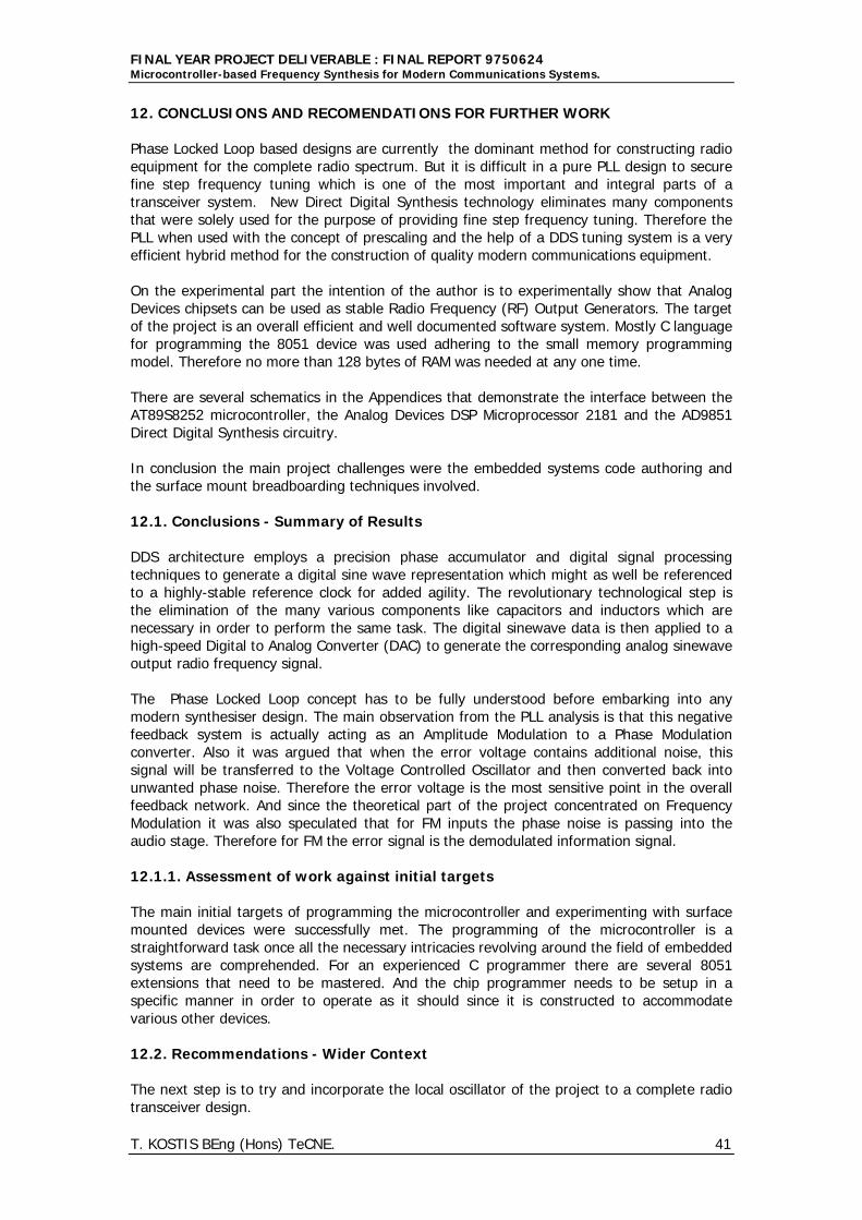
FINAL YEAR PROJECT DELIVERABLE : FINAL REPORT 9750624Microcontroller-based Frequency Synthesis for Modern Communications Systems.
T. KOSTIS BEng (Hons) TeCNE. 41
12. CONCLUSIONS AND RECOMENDATIONS FOR FURTHER WORK
Phase Locked Loop based designs are currently the dominant method for constructing radioequipment for the complete radio spectrum. But it is difficult in a pure PLL design to securefine step frequency tuning which is one of the most important and integral parts of atransceiver system. New Direct Digital Synthesis technology eliminates many componentsthat were solely used for the purpose of providing fine step frequency tuning. Therefore thePLL when used with the concept of prescaling and the help of a DDS tuning system is a veryefficient hybrid method for the construction of quality modern communications equipment.
On the experimental part the intention of the author is to experimentally show that AnalogDevices chipsets can be used as stable Radio Frequency (RF) Output Generators. The targetof the project is an overall efficient and well documented software system. Mostly C languagefor programming the 8051 device was used adhering to the small memory programmingmodel. Therefore no more than 128 bytes of RAM was needed at any one time.
There are several schematics in the Appendices that demonstrate the interface between theAT89S8252 microcontroller, the Analog Devices DSP Microprocessor 2181 and the AD9851Direct Digital Synthesis circuitry.
In conclusion the main project challenges were the embedded systems code authoring andthe surface mount breadboarding techniques involved.
12.1. Conclusions - Summary of Results
DDS architecture employs a precision phase accumulator and digital signal processingtechniques to generate a digital sine wave representation which might as well be referencedto a highly-stable reference clock for added agility. The revolutionary technological step isthe elimination of the many various components like capacitors and inductors which arenecessary in order to perform the same task. The digital sinewave data is then applied to ahigh-speed Digital to Analog Converter (DAC) to generate the corresponding analog sinewaveoutput radio frequency signal.
The Phase Locked Loop concept has to be fully understood before embarking into anymodern synthesiser design. The main observation from the PLL analysis is that this negativefeedback system is actually acting as an Amplitude Modulation to a Phase Modulationconverter. Also it was argued that when the error voltage contains additional noise, thissignal will be transferred to the Voltage Controlled Oscillator and then converted back intounwanted phase noise. Therefore the error voltage is the most sensitive point in the overallfeedback network. And since the theoretical part of the project concentrated on FrequencyModulation it was also speculated that for FM inputs the phase noise is passing into theaudio stage. Therefore for FM the error signal is the demodulated information signal.
12.1.1. Assessment of work against initial targets
The main initial targets of programming the microcontroller and experimenting with surfacemounted devices were successfully met. The programming of the microcontroller is astraightforward task once all the necessary intricacies revolving around the field of embeddedsystems are comprehended. For an experienced C programmer there are several 8051extensions that need to be mastered. And the chip programmer needs to be setup in aspecific manner in order to operate as it should since it is constructed to accommodatevarious other devices.
12.2. Recommendations - Wider Context
The next step is to try and incorporate the local oscillator of the project to a complete radiotransceiver design.
FINAL YEAR PROJECT DELIVERABLE : FINAL REPORT 9750624Microcontroller-based Frequency Synthesis for Modern Communications Systems.
T. KOSTIS BEng (Hons) TeCNE. 42
12.2.1. The Software Radio - Schematic Description
Since the AD9851 was experimentally proved to be a digitally programmable device, thebuilding block this project represents would be best suited in the implementation of aSoftware Radio. A software radio uses algorithms that are hosted by a computer system tocreate channel processor entities. These digital channels can be asked to perform all usualanalog radio functions like mixing and filtering.
The schematic diagram of a software radio receiver as referenced from Slifkin (1999) [31]can be seen in Appendix 15.7.
12.2.2. Spread Spectrum Communications
A signal can be classified as spread spectrum when its RF bandwidth W in Hertz is muchlarger than the required information rate R in bits/sec for a traditional modulation mode.Therefore the bandwidth expansion factor is greater than unity. On the other hand manyspread spectrum users can coexist in the same bandwidth if each user is assigned a differentspreading code. There are two major ways to sustain spread spectrum communications.
Frequency Hopping - Carrier switches in a pseudorandom fashion. Pseudorandom implies asequence that can be recreated by the receiver but has the properties of randomness. Thetime of each carrier block is the dwell time. The receiver knows the order of frequencyswitching and by picking up the successive blocks reassembles the original signal.
Direct Sequence Spread Spectrum - The RF carrier and a pseudo-random pulse train aremixed in a Doubly Balanced Mixer (DBM). Then the RF carrier disappears and is replaced bya noise-like wide band transmission. At the receiver the same pseudorandom sequence iscorrelated with the incoming signal.
AD9851Frequency
Synthesizer
RefClock
30.000MHz
AT89S8252Microcontroller
ControlWords
111.500MHz x4
/40
DBM
MixerPseudorandom
Pulse Train
446.000MHz
2.790MHz
Transmit/ReceiveSwitch
RF Amplifier &Antenna
FM ReceiverBus DirectionControl Mux
IntelligenceSignal
Mixer
111.500MHz
Figure 12.2.2.A. Spread Spectrum Transceiver.
In conclusion spread spectrum communications have four major advantages thatcounterbalance the disadvantages of design complexity. The first advantage is interferencerejection because the entropy of the interference is usually high. Therefore the entropy is noteasily synchronised with the intelligence spread spectrum signal and thus will not appearwhen the signal is correlated with the pseudorandom sequence at the receiver. Secondlytransmissions cannot be easily jammed, that is rendered useless by a counter noise signal atthe same frequency, nor easily detected by an enemy or not authorised otherwise station. Itall results in more secure communications. Third the power density of the transmissionspectrum does not give away a usual modulated signal. The transmission can be easilyhidden from enemy stations using low power and usually is passing for white or colourednoise. Finally the application range is diverse. Apart from secure digital communications,spread spectrum can be used for accurate range finding (time delay) and range rate(velocity) measurements in radar and navigation applications.
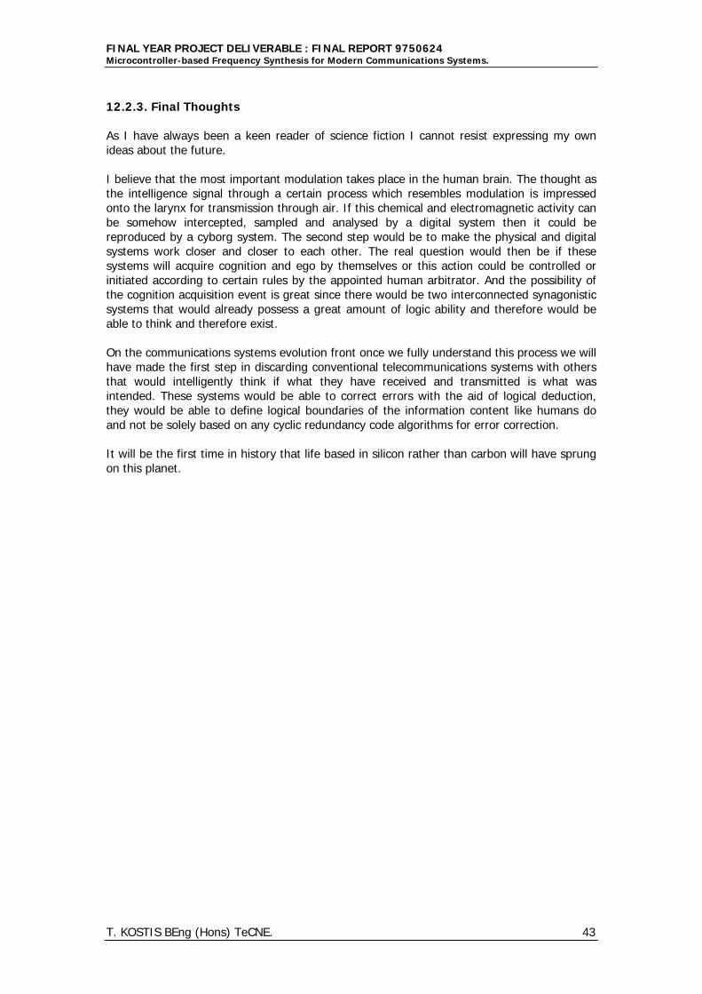
FINAL YEAR PROJECT DELIVERABLE : FINAL REPORT 9750624Microcontroller-based Frequency Synthesis for Modern Communications Systems.
T. KOSTIS BEng (Hons) TeCNE. 43
12.2.3. Final Thoughts
As I have always been a keen reader of science fiction I cannot resist expressing my ownideas about the future.
I believe that the most important modulation takes place in the human brain. The thought asthe intelligence signal through a certain process which resembles modulation is impressedonto the larynx for transmission through air. If this chemical and electromagnetic activity canbe somehow intercepted, sampled and analysed by a digital system then it could bereproduced by a cyborg system. The second step would be to make the physical and digitalsystems work closer and closer to each other. The real question would then be if thesesystems will acquire cognition and ego by themselves or this action could be controlled orinitiated according to certain rules by the appointed human arbitrator. And the possibility ofthe cognition acquisition event is great since there would be two interconnected synagonisticsystems that would already possess a great amount of logic ability and therefore would beable to think and therefore exist.
On the communications systems evolution front once we fully understand this process we willhave made the first step in discarding conventional telecommunications systems with othersthat would intelligently think if what they have received and transmitted is what wasintended. These systems would be able to correct errors with the aid of logical deduction,they would be able to define logical boundaries of the information content like humans doand not be solely based on any cyclic redundancy code algorithms for error correction.
It will be the first time in history that life based in silicon rather than carbon will have sprungon this planet.
FINAL YEAR PROJECT DELIVERABLE : FINAL REPORT 9750624Microcontroller-based Frequency Synthesis for Modern Communications Systems.
T. KOSTIS BEng (Hons) TeCNE. 44
13. BIBLIOGRAPHY AND REFERENCES
[1]. CHAPMAN 1994 The Final Word on the 8051.London : Keil Corporation. (Included in the Keil Demo CD)i. Improving a Microcontroller System using Software Techniques, (70-79).
[2]. MANASSEWITCH 1987 Frequency Synthesisers.New York : Wiley-Interscience. (ISBN 0-471-01116-9)i. Analog Phase Locked Loops, (237-289).ii. Digital Phase Locked Loops, (294-308).iii. Voltage Controlled Oscillators, (379-380).iv. Fast Switching Time Synthesisers - Direct Analog, (578-579).v. Fast Switching Time Synthesisers - Direct Digital, (580-581).
[3]. MILLER 1999 Modern Electronic Communication.New Jersey : Prentice Hall. (ISBN 0-13-927237-2)i. LC Circuits and Oscillators, (29-44).ii. Superheterodyne Receivers, (111-124).iii. Phase Locked Loop FM Transmitter, (212-214).iv. Phase Locked Loop, (243-250).
[4]. BECKER 1997 High-Quality, All-Digital RF Frequency Modulation Generationwith the ADSP-2181 DSP and the AD9850 Direct Digital Synthesiser.Massachusetts : Analog Devices Corporation. (Application Note AN-543 - www.analog.com)
[5]. INTEL 1993 Embedded Microcontrollers and Processors Volume 1.Illinois : Intel Corporation. (Intel Order Number 270645) (ISBN 1-55512-176-4)i. MCS-51 Architectural Overview, (5.2-5.21).ii. MCS-51 Programmer’s Guide and Instruction Set, (6.1-6.76).iii. MCS-51 Hardware Descriptions and Data Sheets, (7.1-7.62).iv. Port Loading, Writing and Interfacing, (7.6-7.8).iv. Power-on Reset Circuit, (7.27-7.28).
[6]. ANALOG DEVICES 1998 CMOS 180MHz DDS Synthesiser AD9851 Datasheet.Massachusetts : Analog Devices Corporation. (www.analog.com)
[7]. REIS 1996 Electronic Project Design and Fabrication.New Jersey : Prentice Hall. (ISBN 0-02-399293-X)i. Computer Aided Design (CAD) and the Design and Drafting Processes (219-229).ii. Project Design and Fabrication using Surface Mount Technology, (234-289).
[8]. EXE 1999 Requirements for success.London : EXE, The Software Developers Magazine Volume 13 Issue 12. (www.exe.co.uk)
[9]. REEHAL 1999 BEng/BSc (Hons) Project Guide EIS_3_801.London : South Bank University.
[10]. WITTS 1942 The Superheterodyne Receiver.London : I. Pitman & Sons, Ltd.i. The Evolution of the Superheterodyne Receiver, (1-11).ii. The General Principles of Superheterodyne Reception, (22-39).
[11]. PEARSON 1992 Basic Communication Theory.New Jersey : Prentice Hall. (ISBN 0-13-061078-X)i. The Need for Modulation.ii. Amplitude Modulation Theory, (92-103).iii. Frequency Modulation Theory, (133-150).iv. Phase Modulation Theory, (190-197).v. Voltage Controlled Oscillators, (158-163).vi. The Phase Locked Loop, (184-185).vii. Amplitude Demodulation, (121-130).viii. Frequency Demodulation, (171-187).
FINAL YEAR PROJECT DELIVERABLE : FINAL REPORT 9750624Microcontroller-based Frequency Synthesis for Modern Communications Systems.
T. KOSTIS BEng (Hons) TeCNE. 45
[12]. ARRL 2000 The ARRL Handbook for Radio Amateurs.Connecticut : ARRL (ISBN 0-87259-183-2)i. Digital Signal Processing, (18.2).ii. Frequency Synthesisers, (14.33).iii. Direct Digital Synthesis, (14.49).
[13]. BARROW 1998 Impossibility.Oxford : Oxford University Press. (ISBN 0-19-851890-0)i. The Big Idea of Unlimited Knowledge, (41-44).ii. Maxwell’s Sorting Demon and The Uncertainty Principle , (142-147).iii. The Futures Market, (72-82).iv. How many discoveries are there still to be made?, (83-84).
[14]. PROAKIS 1995 Digital Communications.New York : McGraw Hill (ISBN 0-070113814-5)i. The Sampling Theorem for Band-Limited Stochastic Processes, (72-74).ii. Spread Spectrum Signals for Digital Communications, (695-752).
[15]. HOROWITZ-HILL 1984 The Art of Electronics.Cambridge : Cambridge University Press.i. Phase Locked Loops, (428-436).ii. Tuned Amplifiers, (568-569).
[16]. SCHULTZ 1998 C and the 8051 - Volume 1.New Jersey : Prentice Hall. (ISBN 0-13-754839-7)i. C or Assembly?, (11-12).ii. 8051 Internal RAM and Input / Output, (21-22).iii. Development and Debugging, (219-267).
[17]. SCHWEBER 1999 Electronic Communications Systems.New Jersey : Simon & Schuster. (ISBN 0-13-780016-9)i. Frequency and Phase Modulation, (143-181).ii. Frequency Synthesisers and Direct Conversion, (424-444).iii. Radar Systems, (635-654).
[18]. MITCHELL-MITCHELL 1992 Introduction to Electronics Design.New Jersey : Prentice Hall. (ISBN 0-13-481748-6)i. Tuned Amplifier, (481-486).ii. Sinewave oscillators and Communication Systems, (601-641).
[19]. RAO 1991 Elements of Engineering Electromagnetics.New Jersey : Prentice Hall. (ISBN 0-13-251604-7)i. Sinusoidally Time-Varying Fields, (30-35).
[20]. NILSSON 1996 Electric Circuits.Wokingham : Addison-Wesley. (ISBN 0-201-40100-2)i. The Fourier Series, (779-830).ii. The Fourier Transform, (831-868).iii. Natural and Step Responses of RLC Circuits, (305-354).iv. The Series RC Circuit as a Low Pass Filter, (664-665).
[21]. ELECTRONICS WORLD 1997 Understanding Phase Noise.Surrey : Reed Business Publication, August 1997. (ISSN 0959-8332)
[22]. HAYKIN 1989 Analog & Digital Communications.Singapore : John Wiley & Sons. (ISBN 0-471-61716-4)i. Fourier Analysis, (13-74).ii. Filtering and Signal Distortion, (83-120).iii. Spectral Density and Correlation, (127-168).iv. Phase Locked Loop and FM Radio, (353-367).
[23]. TAVSANOGLU 1999 An Introduction to Digital Signal Processing.London : South Bank University.
FINAL YEAR PROJECT DELIVERABLE : FINAL REPORT 9750624Microcontroller-based Frequency Synthesis for Modern Communications Systems.
T. KOSTIS BEng (Hons) TeCNE. 46
[24]. BEZANOV 1999 Lecture Notes in Microcomputers and Digital Interfacing.London : South Bank University.
[25]. WEBSTER 1998 Lecture Notes in Circuits and Systems.London : South Bank University.
[26]. FLOYD 1992 Electronic Devices.New Jersey : Prentice Hall. (ISBN 0-13-973769-3)i. Oscillators and the Phase Locked Loop, (860-897).
[27]. RIDDLER 1998 Lecture Notes in Electromagnetics.London : South Bank University.
[28]. PERVEZ 2000 Lecture Notes in Communications Theory.London : South Bank University.
[29]. YAESU 1992 FT-815 430-450 MHz Users Manual.Tokyo : Yaesu Musen Co. Ltd (www.yaesu.com)
[30]. BLAKE 1997 Comprehensive Electronic Communication.Minnesota : West Publishing Company. (ISBN 0-314-20140-8)i. FM Transceivers, (270-271).ii. FM Transmitters, (249-258).iii. FM Receivers, (259-259).iv. Radio-Frequency Oscillators, Mixers and Frequency Synthesisers, (57-95).
[31]. SLIFKIN et. al. 1999 VHF Receiver in DSP.London : Electronics World, October 1999.
[32]. RODDY-COOLEN 1995 Electronic Communications.New Jersey : Prentice Hall. (ISBN 0-13-312083-X)i. Waveform Spectra, (57-92).ii. LC and Voltage-Controlled Oscillators, (195-222).iii. Superheterodyne Receivers, (224-250).
[33]. APPLIED MICROWAVE & WIRELESS 2000 Mini-Circuits Advertisements.Georgia : Noble Publishing, February 2000. (www.amwireless.com)i. Mini-Circuits Power Splitters/Combiners, (2-3).ii. Mini-Circuits Innovative Mixers, (6-6).iii. JCA Technology Low Noise Amplifiers, (9-9).iv. Micrel 900MHz Single Chip RF Receiver, (15-15).
[34]. SURBER et. al. 1998 Single Chip Direct Digital Synthesis vs the Analog PLLs.Massachusetts : Analog Devices Corporation.i. www.analog.com/publications/magazines/dialogue/30-3/single_chip.html
[35]. RS COMPONENTS 1997 Miniature Crystal Oscillator EXO-3.Northants : RS Components. (Issued March 1997 232-4443)
[36]. OSICOM 1999 Direct Digital Frequency Synthesis.New York : Sciteq Technologies.i. www.osicom.com/notes/ddstutor.html
[37]. SOMMERVILLE 1996 Software Engineering.Essex : Addisson-Wesley. (ISBN 0-201-42765-6)
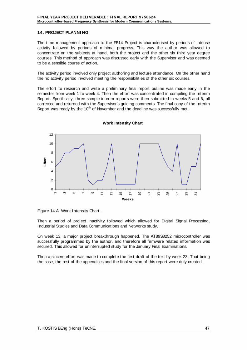
FINAL YEAR PROJECT DELIVERABLE : FINAL REPORT 9750624Microcontroller-based Frequency Synthesis for Modern Communications Systems.
T. KOSTIS BEng (Hons) TeCNE. 47
14. PROJECT PLANNING
The time management approach to the FB14 Project is characterised by periods of intenseactivity followed by periods of minimal progress. This way the author was allowed toconcentrate on the subjects at hand, both the project and the other six third year degreecourses. This method of approach was discussed early with the Supervisor and was deemedto be a sensible course of action.
The activity period involved only project authoring and lecture attendance. On the other handthe no activity period involved meeting the responsibilities of the other six courses.
The effort to research and write a preliminary final report outline was made early in thesemester from week 1 to week 4. Then the effort was concentrated in compiling the InterimReport. Specifically, three sample interim reports were then submitted in weeks 5 and 6, allcorrected and returned with the Supervisor’s guiding comments. The final copy of the InterimReport was ready by the 10th of November and the deadline was successfully met.
Work Intensity Chart
0
2
4
6
8
10
12
1 3 5 7 9 11 13 15 17 19 21 23 25 27 29 31Weeks
Eff
ort
Figure 14.A. Work Intensity Chart.
Then a period of project inactivity followed which allowed for Digital Signal Processing,Industrial Studies and Data Communications and Networks study.
On week 13, a major project breakthrough happened. The AT89S8252 microcontroller wassuccessfully programmed by the author, and therefore all firmware related information wassecured. This allowed for uninterrupted study for the January Final Examinations.
Then a sincere effort was made to complete the first draft of the text by week 23. That beingthe case, the rest of the appendices and the final version of this report were duly created.
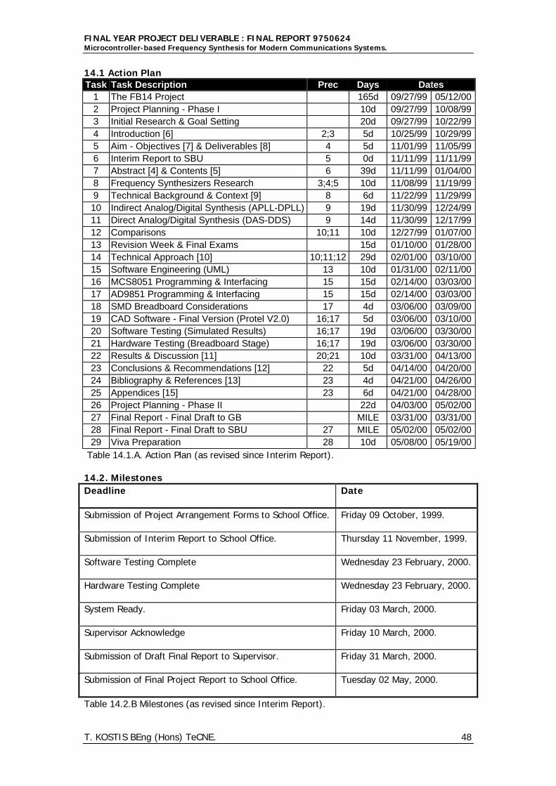
FINAL YEAR PROJECT DELIVERABLE : FINAL REPORT 9750624Microcontroller-based Frequency Synthesis for Modern Communications Systems.
T. KOSTIS BEng (Hons) TeCNE. 48
14.1 Action PlanTask Task Description Prec Days Dates
1 The FB14 Project 165d 09/27/99 05/12/002 Project Planning - Phase I 10d 09/27/99 10/08/993 Initial Research & Goal Setting 20d 09/27/99 10/22/994 Introduction [6] 2;3 5d 10/25/99 10/29/995 Aim - Objectives [7] & Deliverables [8] 4 5d 11/01/99 11/05/996 Interim Report to SBU 5 0d 11/11/99 11/11/997 Abstract [4] & Contents [5] 6 39d 11/11/99 01/04/008 Frequency Synthesizers Research 3;4;5 10d 11/08/99 11/19/999 Technical Background & Context [9] 8 6d 11/22/99 11/29/9910 Indirect Analog/Digital Synthesis (APLL-DPLL) 9 19d 11/30/99 12/24/9911 Direct Analog/Digital Synthesis (DAS-DDS) 9 14d 11/30/99 12/17/9912 Comparisons 10;11 10d 12/27/99 01/07/0013 Revision Week & Final Exams 15d 01/10/00 01/28/0014 Technical Approach [10] 10;11;12 29d 02/01/00 03/10/0015 Software Engineering (UML) 13 10d 01/31/00 02/11/0016 MCS8051 Programming & Interfacing 15 15d 02/14/00 03/03/0017 AD9851 Programming & Interfacing 15 15d 02/14/00 03/03/0018 SMD Breadboard Considerations 17 4d 03/06/00 03/09/0019 CAD Software - Final Version (Protel V2.0) 16;17 5d 03/06/00 03/10/0020 Software Testing (Simulated Results) 16;17 19d 03/06/00 03/30/0021 Hardware Testing (Breadboard Stage) 16;17 19d 03/06/00 03/30/0022 Results & Discussion [11] 20;21 10d 03/31/00 04/13/0023 Conclusions & Recommendations [12] 22 5d 04/14/00 04/20/0024 Bibliography & References [13] 23 4d 04/21/00 04/26/0025 Appendices [15] 23 6d 04/21/00 04/28/0026 Project Planning - Phase II 22d 04/03/00 05/02/0027 Final Report - Final Draft to GB MILE 03/31/00 03/31/0028 Final Report - Final Draft to SBU 27 MILE 05/02/00 05/02/0029 Viva Preparation 28 10d 05/08/00 05/19/00
Table 14.1.A. Action Plan (as revised since Interim Report).
14.2. MilestonesDeadline Date
Submission of Project Arrangement Forms to School Office. Friday 09 October, 1999.
Submission of Interim Report to School Office. Thursday 11 November, 1999.
Software Testing Complete Wednesday 23 February, 2000.
Hardware Testing Complete Wednesday 23 February, 2000.
System Ready. Friday 03 March, 2000.
Supervisor Acknowledge Friday 10 March, 2000.
Submission of Draft Final Report to Supervisor. Friday 31 March, 2000.
Submission of Final Project Report to School Office. Tuesday 02 May, 2000.
Table 14.2.B Milestones (as revised since Interim Report).
FINAL YEAR PROJECT DELIVERABLE : FINAL REPORT 9750624Microcontroller-based Frequency Synthesis for Modern Communications Systems.
T. KOSTIS BEng (Hons) TeCNE. 49

FINAL YEAR PROJECT DELIVERABLE : FINAL REPORT 9750624Microcontroller-based Frequency Synthesis for Modern Communications Systems.
T. KOSTIS BEng (Hons) TeCNE. 50
14.4. Gantt Chart
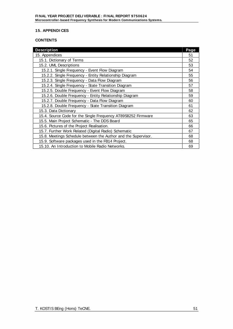
FINAL YEAR PROJECT DELIVERABLE : FINAL REPORT 9750624Microcontroller-based Frequency Synthesis for Modern Communications Systems.
T. KOSTIS BEng (Hons) TeCNE. 51
15. APPENDICES
CONTENTS
Description Page15. Appendices 51 15.1. Dictionary of Terms 52 15.2. UML Descriptions 53 15.2.1. Single Frequency - Event Flow Diagram 54 15.2.2. Single Frequency - Entity Relationship Diagram 55 15.2.3. Single Frequency - Data Flow Diagram 56 15.2.4. Single Frequency - State Transition Diagram 57 15.2.5. Double Frequency - Event Flow Diagram 58 15.2.6. Double Frequency - Entity Relationship Diagram 59 15.2.7. Double Frequency - Data Flow Diagram 60 15.2.8. Double Frequency - State Transition Diagram 61 15.3. Data Dictionary 62 15.4. Source Code for the Single Frequency AT89S8252 Firmware 63 15.5. Main Project Schematic - The DDS Board 65 15.6. Pictures of the Project Realisation. 66 15.7. Further Work Related (Digital Radio) Schematic 67 15.8. Meetings Schedule between the Author and the Supervisor. 68 15.9. Software packages used in the FB14 Project. 68 15.10. An Introduction to Mobile Radio Networks. 69
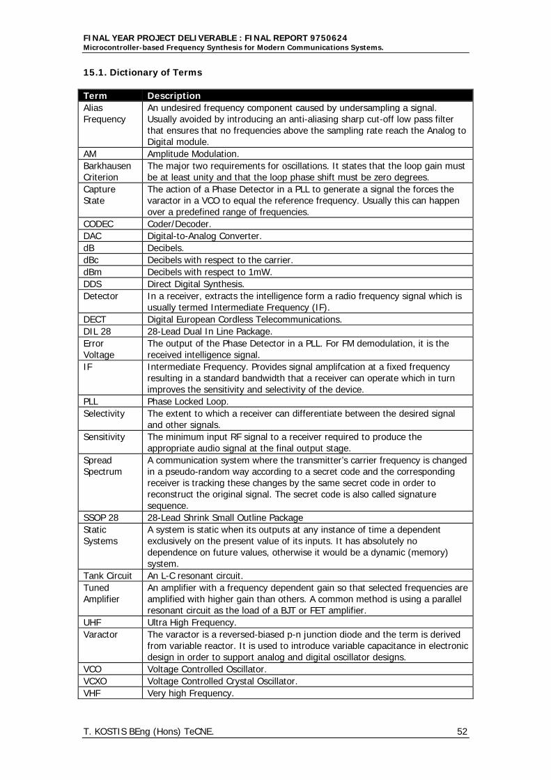
FINAL YEAR PROJECT DELIVERABLE : FINAL REPORT 9750624Microcontroller-based Frequency Synthesis for Modern Communications Systems.
T. KOSTIS BEng (Hons) TeCNE. 52
15.1. Dictionary of Terms
Term DescriptionAliasFrequency
An undesired frequency component caused by undersampling a signal.Usually avoided by introducing an anti-aliasing sharp cut-off low pass filterthat ensures that no frequencies above the sampling rate reach the Analog toDigital module.
AM Amplitude Modulation.BarkhausenCriterion
The major two requirements for oscillations. It states that the loop gain mustbe at least unity and that the loop phase shift must be zero degrees.
CaptureState
The action of a Phase Detector in a PLL to generate a signal the forces thevaractor in a VCO to equal the reference frequency. Usually this can happenover a predefined range of frequencies.
CODEC Coder/Decoder.DAC Digital-to-Analog Converter.dB Decibels.dBc Decibels with respect to the carrier.dBm Decibels with respect to 1mW.DDS Direct Digital Synthesis.Detector In a receiver, extracts the intelligence form a radio frequency signal which is
usually termed Intermediate Frequency (IF).DECT Digital European Cordless Telecommunications.DIL 28 28-Lead Dual In Line Package.ErrorVoltage
The output of the Phase Detector in a PLL. For FM demodulation, it is thereceived intelligence signal.
IF Intermediate Frequency. Provides signal amplifcation at a fixed frequencyresulting in a standard bandwidth that a receiver can operate which in turnimproves the sensitivity and selectivity of the device.
PLL Phase Locked Loop.Selectivity The extent to which a receiver can differentiate between the desired signal
and other signals.Sensitivity The minimum input RF signal to a receiver required to produce the
appropriate audio signal at the final output stage.SpreadSpectrum
A communication system where the transmitter’s carrier frequency is changedin a pseudo-random way according to a secret code and the correspondingreceiver is tracking these changes by the same secret code in order toreconstruct the original signal. The secret code is also called signaturesequence.
SSOP 28 28-Lead Shrink Small Outline PackageStaticSystems
A system is static when its outputs at any instance of time a dependentexclusively on the present value of its inputs. It has absolutely nodependence on future values, otherwise it would be a dynamic (memory)system.
Tank Circuit An L-C resonant circuit.TunedAmplifier
An amplifier with a frequency dependent gain so that selected frequencies areamplified with higher gain than others. A common method is using a parallelresonant circuit as the load of a BJT or FET amplifier.
UHF Ultra High Frequency.Varactor The varactor is a reversed-biased p-n junction diode and the term is derived
from variable reactor. It is used to introduce variable capacitance in electronicdesign in order to support analog and digital oscillator designs.
VCO Voltage Controlled Oscillator.VCXO Voltage Controlled Crystal Oscillator.VHF Very high Frequency.

FINAL YEAR PROJECT DELIVERABLE : FINAL REPORT 9750624Microcontroller-based Frequency Synthesis for Modern Communications Systems.
T. KOSTIS BEng (Hons) TeCNE. 53
15.2. UML Descriptions
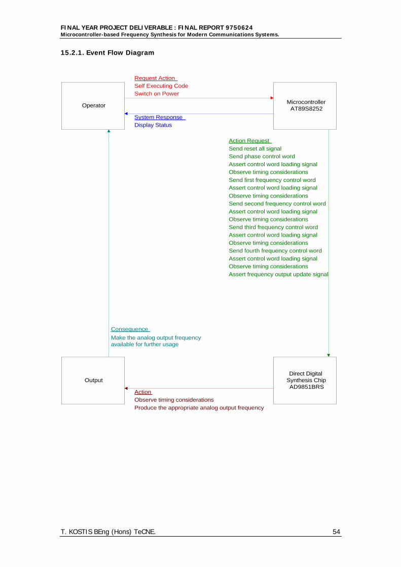
FINAL YEAR PROJECT DELIVERABLE : FINAL REPORT 9750624Microcontroller-based Frequency Synthesis for Modern Communications Systems.
T. KOSTIS BEng (Hons) TeCNE. 54
15.2.1. Event Flow Diagram
OperatorMicrocontroller
AT89S8252
Direct DigitalSynthesis ChipAD9851BRS
Output
Request ActionSelf Executing CodeSwitch on Power
System ResponseDisplay Status
Consequence
Make the analog output frequencyavailable for further usage
Action
Produce the appropriate analog output frequency
Action RequestSend reset all signalSend phase control word
Send first frequency control word
Send second frequency control word
Send third frequency control word
Send fourth frequency control word
Assert control word loading signal
Assert control word loading signal
Assert control word loading signal
Assert control word loading signal
Assert control word loading signal
Assert frequency output update signal
Observe timing considerations
Observe timing considerations
Observe timing considerations
Observe timing considerations
Observe timing considerations
Observe timing considerations
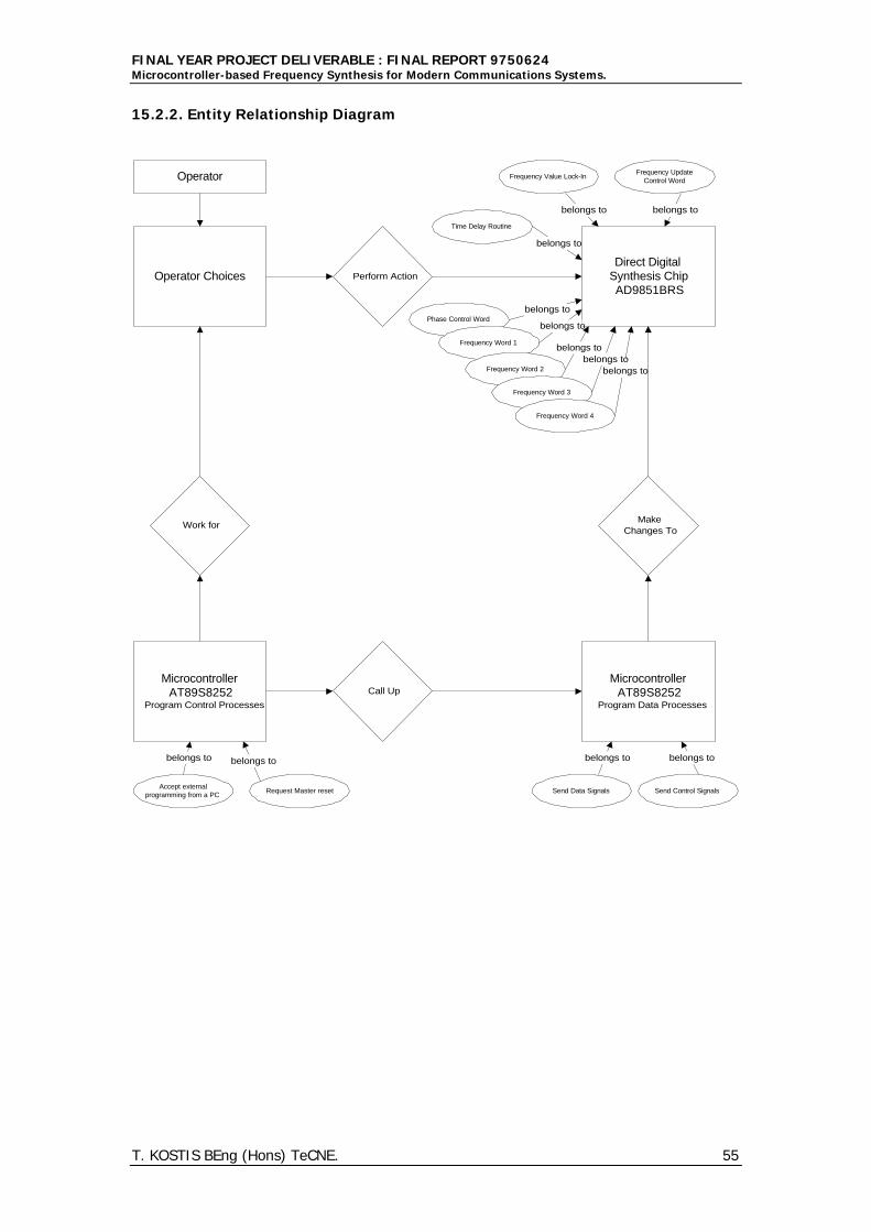
FINAL YEAR PROJECT DELIVERABLE : FINAL REPORT 9750624Microcontroller-based Frequency Synthesis for Modern Communications Systems.
T. KOSTIS BEng (Hons) TeCNE. 55
15.2.2. Entity Relationship Diagram
Operator
MicrocontrollerAT89S8252
Program Control Processes
Operator ChoicesDirect Digital
Synthesis ChipAD9851BRS
Perform Action
Work for
Call Up
MakeChanges To
Accept externalprogramming from a PC
belongs to
Request Master reset
belongs to
MicrocontrollerAT89S8252
Program Data Processes
Phase Control Wordbelongs to
Frequency UpdateControl Word
belongs to
Frequency Word 1
belongs to
Frequency Word 2
Frequency Word 3
Frequency Word 4
belongs to
belongs tobelongs to
Frequency Value Lock-In
belongs to
Time Delay Routine
belongs to
Send Data Signals
belongs to
Send Control Signals
belongs to
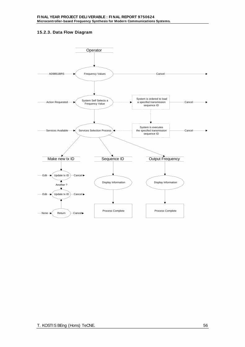
FINAL YEAR PROJECT DELIVERABLE : FINAL REPORT 9750624Microcontroller-based Frequency Synthesis for Modern Communications Systems.
T. KOSTIS BEng (Hons) TeCNE. 56
15.2.3. Data Flow Diagram
Frequency Values
Operator
System Self Selects aFrequency Value
Services Selection Process
Action RequestedSystem is ordered to loada specifed transmission
sequence ID
AD9851BRS
System is executesthe specifed transmission
sequence IDServices Available
Make new tx ID Sequence ID
Display Information
Process Complete
Output Frequency
Display Information
Process Complete
Update tx ID
Cancel
Cancel
Cancel
Edit Cancel
Update tx IDEdit Cancel
Another ?
ReturnNone Cancel
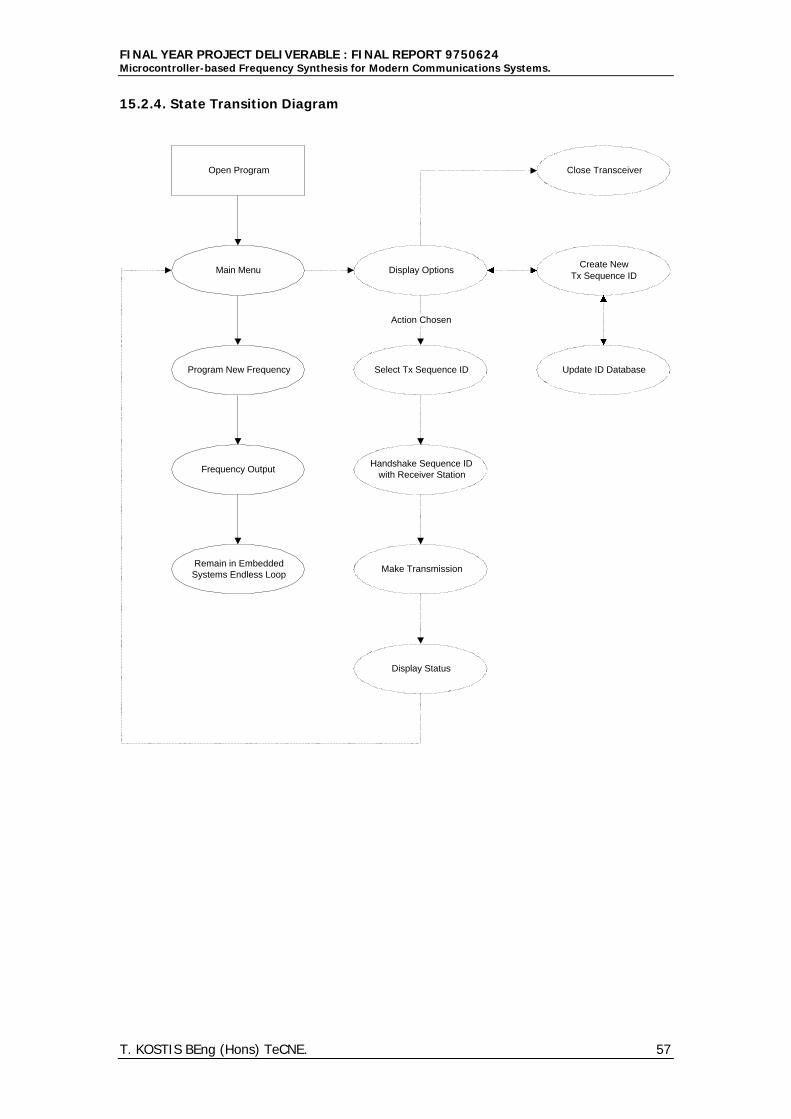
FINAL YEAR PROJECT DELIVERABLE : FINAL REPORT 9750624Microcontroller-based Frequency Synthesis for Modern Communications Systems.
T. KOSTIS BEng (Hons) TeCNE. 57
15.2.4. State Transition Diagram
Open Program
Main Menu
Action Chosen
Program New Frequency
Frequency Output
Remain in EmbeddedSystems Endless Loop
Display OptionsCreate New
Tx Sequence ID
Update ID DatabaseSelect Tx Sequence ID
Handshake Sequence IDwith Receiver Station
Make Transmission
Display Status
Close Transceiver
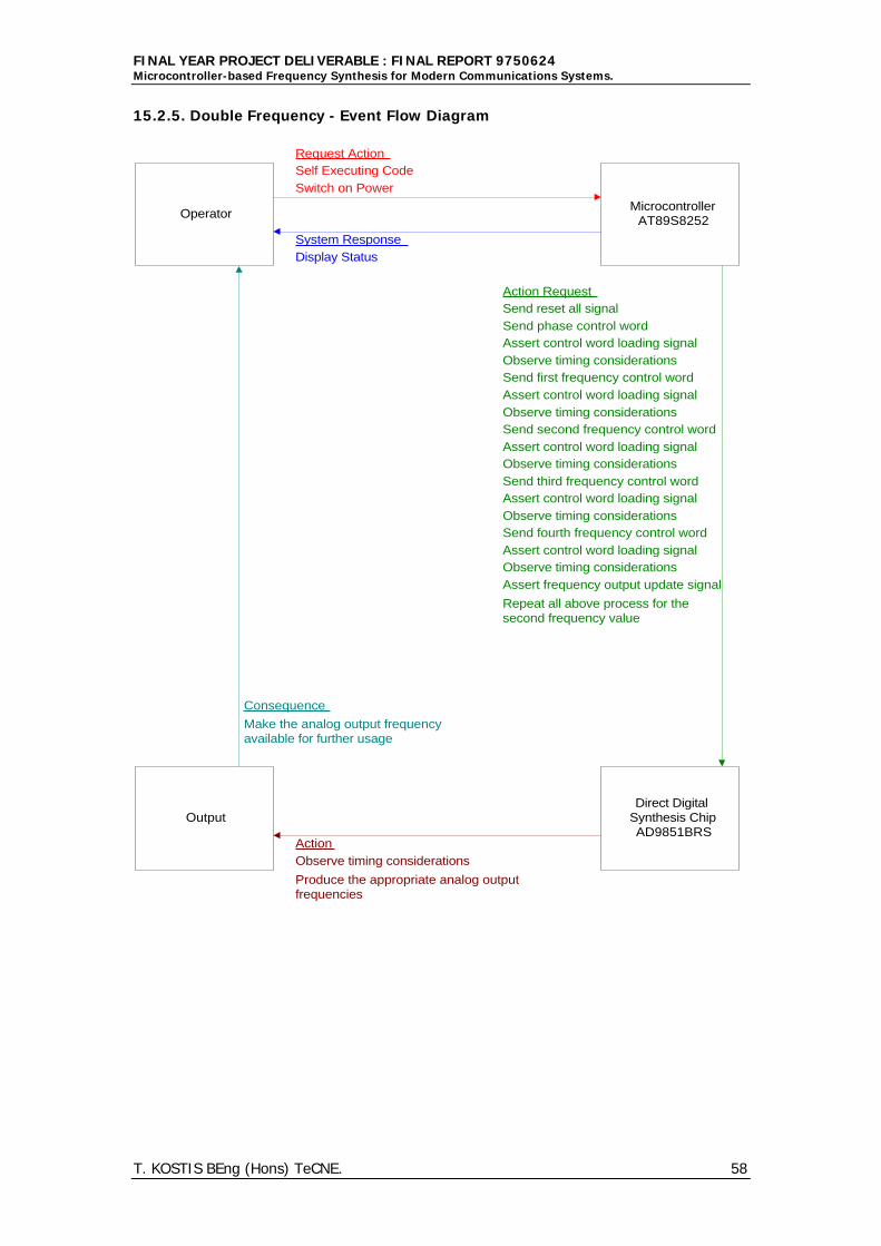
FINAL YEAR PROJECT DELIVERABLE : FINAL REPORT 9750624Microcontroller-based Frequency Synthesis for Modern Communications Systems.
T. KOSTIS BEng (Hons) TeCNE. 58
15.2.5. Double Frequency - Event Flow Diagram
OperatorMicrocontroller
AT89S8252
Direct DigitalSynthesis ChipAD9851BRS
Output
Request ActionSelf Executing CodeSwitch on Power
System ResponseDisplay Status
Consequence
Make the analog output frequencyavailable for further usage
Action
Produce the appropriate analog outputfrequencies
Action RequestSend reset all signalSend phase control word
Send first frequency control word
Send second frequency control word
Send third frequency control word
Send fourth frequency control word
Assert control word loading signal
Assert control word loading signal
Assert control word loading signal
Assert control word loading signal
Assert control word loading signal
Assert frequency output update signal
Observe timing considerations
Observe timing considerations
Observe timing considerations
Observe timing considerations
Observe timing considerations
Observe timing considerations
Repeat all above process for thesecond frequency value
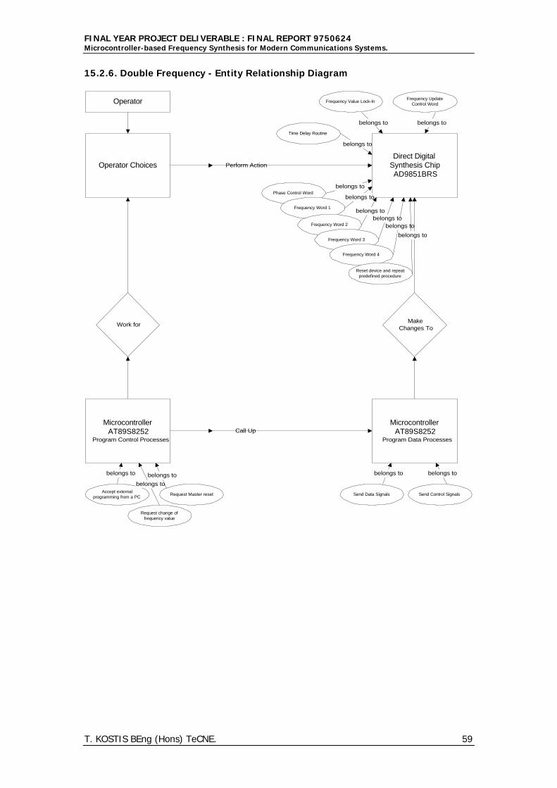
FINAL YEAR PROJECT DELIVERABLE : FINAL REPORT 9750624Microcontroller-based Frequency Synthesis for Modern Communications Systems.
T. KOSTIS BEng (Hons) TeCNE. 59
15.2.6. Double Frequency - Entity Relationship Diagram
Operator
MicrocontrollerAT89S8252
Program Control Processes
Operator ChoicesDirect Digital
Synthesis ChipAD9851BRS
Perform Action
Work for
Call Up
MakeChanges To
Accept externalprogramming from a PC
belongs to
Request Master reset
belongs to
MicrocontrollerAT89S8252
Program Data Processes
Phase Control Wordbelongs to
Frequency UpdateControl Word
belongs to
Frequency Word 1
belongs to
Frequency Word 2
Frequency Word 3
Frequency Word 4
belongs to
belongs tobelongs to
Frequency Value Lock-In
belongs to
Time Delay Routine
belongs to
Send Data Signals
belongs to
Send Control Signals
belongs to
Reset device and repeatpredefined procedure
belongs to
Request change offrequency value
belongs to
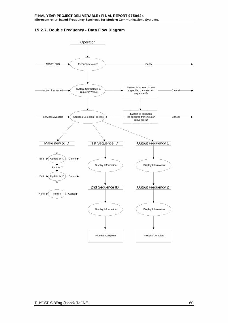
FINAL YEAR PROJECT DELIVERABLE : FINAL REPORT 9750624Microcontroller-based Frequency Synthesis for Modern Communications Systems.
T. KOSTIS BEng (Hons) TeCNE. 60
15.2.7. Double Frequency - Data Flow Diagram
Frequency Values
Operator
System Self Selects aFrequency Value
Services Selection Process
Action RequestedSystem is ordered to loada specifed transmission
sequence ID
AD9851BRS
System is executesthe specifed transmission
sequence IDServices Available
Make new tx ID 1st Sequence ID
Display Information
Process Complete
Output Frequency 1
Display Information
Process Complete
Update tx ID
Cancel
Cancel
Cancel
Edit Cancel
Update tx IDEdit Cancel
Another ?
ReturnNone Cancel
2nd Sequence ID
Display Information
Output Frequency 2
Display Information
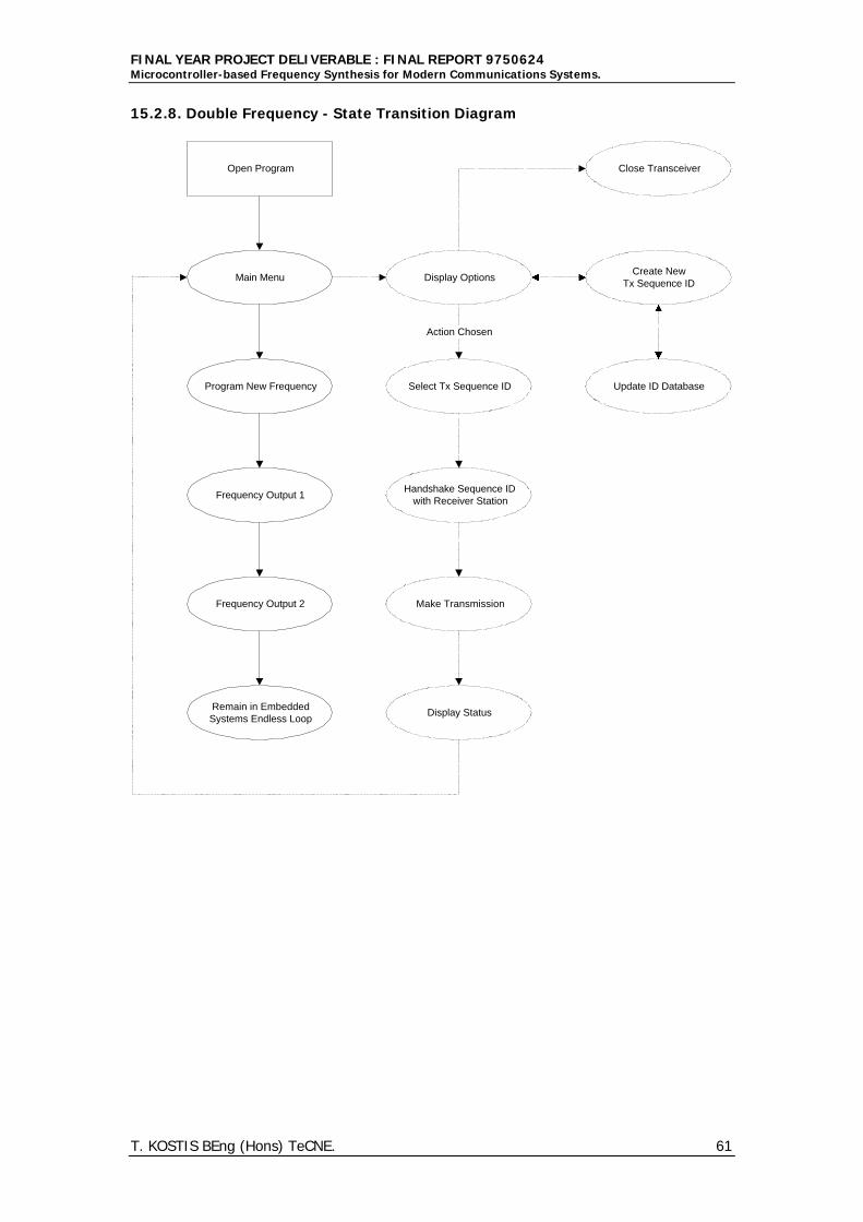
FINAL YEAR PROJECT DELIVERABLE : FINAL REPORT 9750624Microcontroller-based Frequency Synthesis for Modern Communications Systems.
T. KOSTIS BEng (Hons) TeCNE. 61
15.2.8. Double Frequency - State Transition Diagram
Open Program
Main Menu
Action Chosen
Program New Frequency
Frequency Output 1
Remain in EmbeddedSystems Endless Loop
Display OptionsCreate New
Tx Sequence ID
Update ID DatabaseSelect Tx Sequence ID
Handshake Sequence IDwith Receiver Station
Make Transmission
Display Status
Close Transceiver
Frequency Output 2
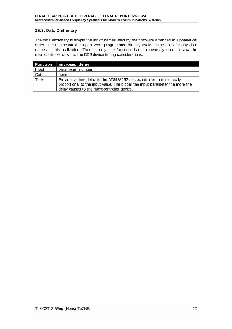
FINAL YEAR PROJECT DELIVERABLE : FINAL REPORT 9750624Microcontroller-based Frequency Synthesis for Modern Communications Systems.
T. KOSTIS BEng (Hons) TeCNE. 62
15.3. Data Dictionary
The data dictionary is simply the list of names used by the firmware arranged in alphabeticalorder. The microcontroller’s port were programmed directly avoiding the use of many datanames in this realization. There is only one function that is repeatedly used to slow themicrocontroller down to the DDS device timing considerations.
Function microsec_delayInput parameter [number]Output noneTask Provides a time delay to the AT89S8252 microcontroller that is directly
proportional to the input value. The bigger the input parameter the more thedelay caused to the microcontroller device.
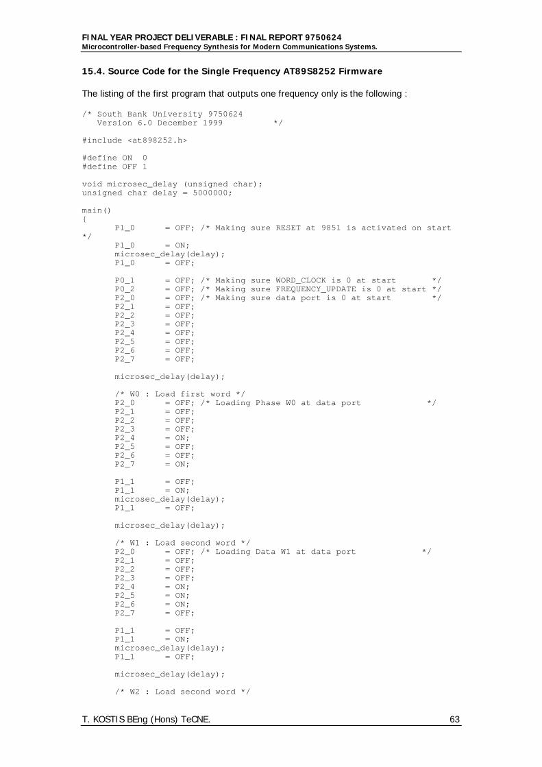
FINAL YEAR PROJECT DELIVERABLE : FINAL REPORT 9750624Microcontroller-based Frequency Synthesis for Modern Communications Systems.
T. KOSTIS BEng (Hons) TeCNE. 63
15.4. Source Code for the Single Frequency AT89S8252 Firmware
The listing of the first program that outputs one frequency only is the following :
/* South Bank University 9750624 Version 6.0 December 1999 */
#include <at898252.h>
#define ON 0#define OFF 1
void microsec_delay (unsigned char);unsigned char delay = 5000000;
main(){
P1_0 = OFF; /* Making sure RESET at 9851 is activated on start*/
P1_0 = ON;microsec_delay(delay);P1_0 = OFF;
P0_1 = OFF; /* Making sure WORD_CLOCK is 0 at start */P0_2 = OFF; /* Making sure FREQUENCY_UPDATE is 0 at start */P2_0 = OFF; /* Making sure data port is 0 at start */P2_1 = OFF;P2_2 = OFF;P2_3 = OFF;P2_4 = OFF;P2_5 = OFF;P2_6 = OFF;P2_7 = OFF;
microsec_delay(delay);
/* W0 : Load first word */P2_0 = OFF; /* Loading Phase W0 at data port */P2_1 = OFF;P2_2 = OFF;P2_3 = OFF;P2_4 = ON;P2_5 = OFF;P2_6 = OFF;P2_7 = ON;
P1_1 = OFF;P1_1 = ON;microsec_delay(delay);P1_1 = OFF;
microsec_delay(delay);
/* W1 : Load second word */P2_0 = OFF; /* Loading Data W1 at data port */P2_1 = OFF;P2_2 = OFF;P2_3 = OFF;P2_4 = ON;P2_5 = ON;P2_6 = ON;P2_7 = OFF;
P1_1 = OFF;P1_1 = ON;microsec_delay(delay);P1_1 = OFF;
microsec_delay(delay);
/* W2 : Load second word */
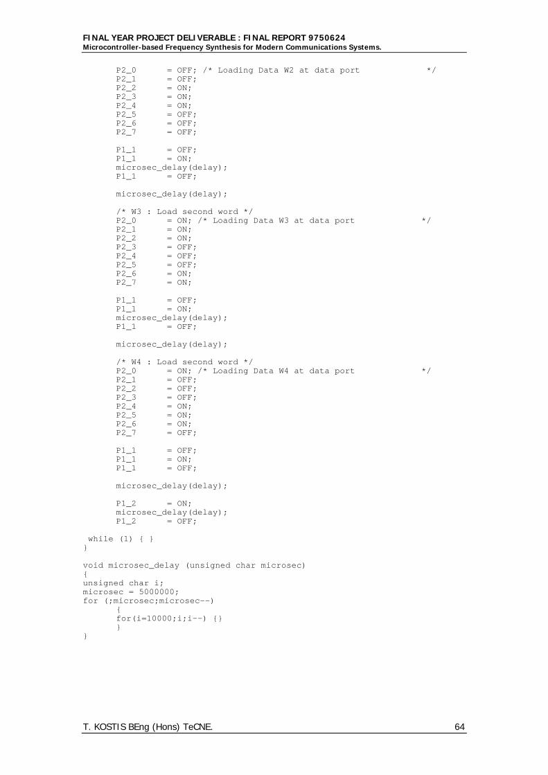
FINAL YEAR PROJECT DELIVERABLE : FINAL REPORT 9750624Microcontroller-based Frequency Synthesis for Modern Communications Systems.
T. KOSTIS BEng (Hons) TeCNE. 64
P2_0 = OFF; /* Loading Data W2 at data port */P2_1 = OFF;P2_2 = ON;P2_3 = ON;P2_4 = ON;P2_5 = OFF;P2_6 = OFF;P2_7 = OFF;
P1_1 = OFF;P1_1 = ON;microsec_delay(delay);P1_1 = OFF;
microsec_delay(delay);
/* W3 : Load second word */P2_0 = ON; /* Loading Data W3 at data port */P2_1 = ON;P2_2 = ON;P2_3 = OFF;P2_4 = OFF;P2_5 = OFF;P2_6 = ON;P2_7 = ON;
P1_1 = OFF;P1_1 = ON;microsec_delay(delay);P1_1 = OFF;
microsec_delay(delay);
/* W4 : Load second word */P2_0 = ON; /* Loading Data W4 at data port */P2_1 = OFF;P2_2 = OFF;P2_3 = OFF;P2_4 = ON;P2_5 = ON;P2_6 = ON;P2_7 = OFF;
P1_1 = OFF;P1_1 = ON;P1_1 = OFF;
microsec_delay(delay);
P1_2 = ON;microsec_delay(delay);P1_2 = OFF;
while (1) { }}
void microsec_delay (unsigned char microsec){unsigned char i;microsec = 5000000;for (;microsec;microsec--)
{for(i=10000;i;i--) {}}
}
FINAL YEAR PROJECT DELIVERABLE : FINAL REPORT 9750624Microcontroller-based Frequency Synthesis for Modern Communications Systems.
T. KOSTIS BEng (Hons) TeCNE. 65
15.5. Main Project Schematic - The DDS Board
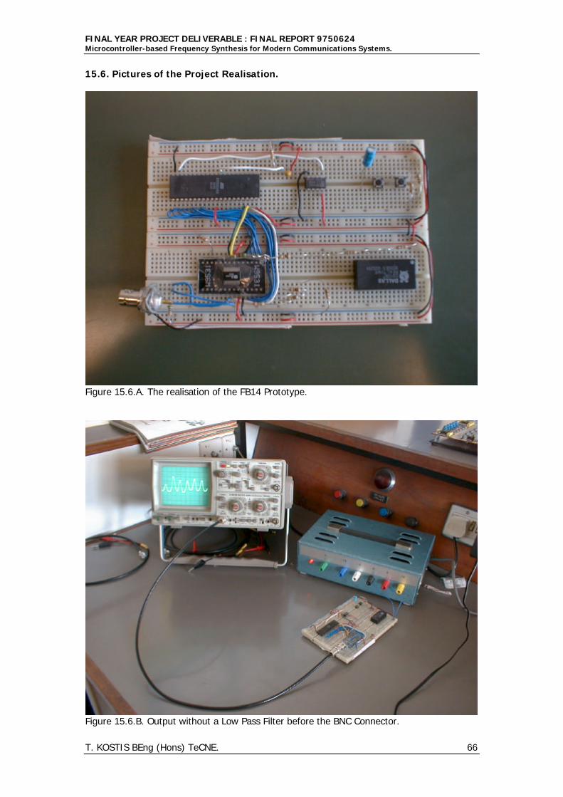
FINAL YEAR PROJECT DELIVERABLE : FINAL REPORT 9750624Microcontroller-based Frequency Synthesis for Modern Communications Systems.
T. KOSTIS BEng (Hons) TeCNE. 66
15.6. Pictures of the Project Realisation.
Figure 15.6.A. The realisation of the FB14 Prototype.
Figure 15.6.B. Output without a Low Pass Filter before the BNC Connector.
FINAL YEAR PROJECT DELIVERABLE : FINAL REPORT 9750624Microcontroller-based Frequency Synthesis for Modern Communications Systems.
T. KOSTIS BEng (Hons) TeCNE. 67
15.7. Further Work Related (Digital Radio) Schematic
FINAL YEAR PROJECT DELIVERABLE : FINAL REPORT 9750624Microcontroller-based Frequency Synthesis for Modern Communications Systems.
T. KOSTIS BEng (Hons) TeCNE. 68
15.8. Meetings Schedule between the Author and the Supervisor.
Description DateFirst meeting - Informal. 30/09/99Discussed report format and change of title. Approved type of logbook. 07/10/99DDS Focusing. PLL coverage. 15/10/99Programming the AT89S8252 device. First firmware version. 27/10/99Schematic and components. 10/11/99Interim report results. Second Firmware version. 01/12/99DSP Focusing. Digital Oscillators, Filters. Abstract practice. DDS Theory. 08/12/99Design Phase. Object-orientation. Procedural Approach. 15/12/99UML Concepts. Superheterodyne Theory. 03/02/00Successful testing of the breadboard in Communications Laboratory. 07/02/00Prescaling Theory. Experiments continue. 07/03/00Results and Discussion. Subsequent firmware versions. 13/03/00Software Engineering and Feedback. 20/03/00Testing Phase. 27/03/00Final Meeting. Overall Assessment. 03/04/00
15.9. Software packages used in the FB14 Project.
The complete list of software used for this project is as follows :
Name Description1.0 Microsoft Windows 98 SE Operating System.
2.0 Microsoft Word 95 Word Processor.2.1 Publicon Ver. 0.9 Mathematical Formula Editor.2.2 Visio 95 Block Diagram Authoring.2.3 Microsoft Project 95 Time & Resources Management.2.4 Microsoft Excel 95 Spreadsheet.
3.0 Franklin Software C with 8051 extensions.3.1 Keil PK51 Software C with 8051 extensions.
4.0 SELECT for Windows Ver. 3.10 UML Documentation.
5.0 Protel Schematic for Windows Ver. 2.0 Schematic Editor.5.1 Protel Library for Windows Ver. 2.0 Component Editor.
6.0 Atmel AVR Studio Version 1.40 Microcontroller Chip Programming.
7.0 RS Catalog CD-ROM Component Selection and Sourcing.
8.0 Adobe Photoshop Ver. 4.0 Picture Manipulation.

FINAL YEAR PROJECT DELIVERABLE : FINAL REPORT 9750624Microcontroller-based Frequency Synthesis for Modern Communications Systems.
T. KOSTIS BEng (Hons) TeCNE. 69
SOUTH BANK UNIVERSITY
School of Electrical Electronic and Information Engineering
THEODOROS KOSTIS 9750624BEng (Hons) Telecommunications and Computer Networks Engineering
COURSE TITLE:TELECOMMUNICATIONS AND BROADBAND SYSTEMS
COURSE CODE : E-CI-3-833
COURSE YEAR : 3
LECTURER : DR. X. PENG
REPORT TITLE : MOBILE RADIO NETWORKS
DATE : 19 MAY 2000
1. ABSTRACT
The growth rate of mobile communications systems is exponentially increasing. The globalsociety is becoming more aware of the advantages of mobile radio networks and thetraditional monopolies and oligopolies of the telecommunications industry are quicklyreplaced by a competition that is devoted to provide low cost mobile private and publicaccess to the global networks. This report is an introduction to mobile radio networksengineering and standards.

FINAL YEAR PROJECT DELIVERABLE : FINAL REPORT 9750624Microcontroller-based Frequency Synthesis for Modern Communications Systems.
T. KOSTIS BEng (Hons) TeCNE. 70
2. CONTENTSDescription Page1. Abstract 12. Contents 23. Introduction 34. Discussion 3 4.1. Propagation Modelling in Mobile Communications 3 4.2. Broadband Communications for Fixed and Mobile Networks 4 4.3. Multiplexing 5 4.4. Modulation 5 4.5 Spread Spectrum Communications 6 4.6. Medium Access Control for Wireless Communications 6 4.6.1. Space Division Multiple Access (SDMA) 7 4.6.2. Frequency Division Multiple Access (FDMA) 7 4.6.3. Time Division Multiple Access (TDMA) 7 4.6.4. Code Division Multiple Access (CDMA) 7 4.7. Telecommunications Systems 7 4.7.1. Cellular Telephony - The GSM Standard 7 4.7.2. Cordless Telephony - The DECT Standard 8 4.7.3. The Terrestrial Trunked Radio (TETRA) System 8 4.7.4. UMTS and IMT-2000 8 4.7.5. Personal Satellite Communications 8 4.7.6. Broadcast Systems 8 4.7.7. Wireless Local Area Networks - IEEE 802.11, HIPERLAN and Bluetooth 9 4.7.8. Wireless ATM Systems 95. Conclusion 106. Bibliography and References 11
List of FiguresIndex Description Page4.1.A. Multipath Fading. 34.4.A. Amplitude Shift Keying (ASK). 54.4.B. Frequency Shift Keying (FSK). 54.4.C. Phase Shift Keying (PSK). 54.6.A. Hidden Wireless Terminals. A is hidden form C and vice versa. 64.6.B. Exposed Wireless Terminals. C is exposed to B. 64.6.C. Near and Far Wireless Terminals. A is blocked by C. 64.7.8.A. Example Reference Model for Wireless Access. 94.7.8.B. WATM Reference Model and corresponding wireless protocol layers. 10
List of TablesIndex Description Page4.7.7.A. HIPERLAN Types. 9

FINAL YEAR PROJECT DELIVERABLE : FINAL REPORT 9750624Microcontroller-based Frequency Synthesis for Modern Communications Systems.
T. KOSTIS BEng (Hons) TeCNE. 71
3. INTRODUCTION
The fixed telephone network has been the de facto communications standard for manydecades. And the classical telephone handset with its cabling attaching to our wall at homeor at work is the personification of immobility. During the 1970s transistor technologyallowed the use of wireless handsets that could hold a full-duplex transmission for up toseveral meters. But the conversation was not only of poor quality but could be easilyintercepted by any other third party with a general purpose scanner in the 27 to 29 MHzband. Blake 1997 [01] (731) explains that this technology in parallel allowed the birth of theCitizen’s Band (CB) systems which represented the first personal mobile radiocommunications network. But the absence of any licence requirements for operating theabove two systems and their inherent analog continuous baseband nature introduced majorinterference and operating problems.
The major telecommunications organisations then agreed to set out certain standards so thatwireless technology could be used to the maximum benefit of both the user and the networkoperator. Technological breakthroughs in the microwave industry allowed the use of otherhigher frequencies. And telecommunications organisations started to forge strategic alliancesfor the standardised development of new equipment. This report will focus on the protocols,the infrastructure, the applications and the regulation of mobile radio networks as they havebeen currently developed.
4. DISCUSSION
4.1. Propagation Modelling in Mobile Communications
Usually no direct path exists between two communicating stations and the communicationdepends on single and multiple reflections from all the surrounding objects. Dunlop 1994[02] (524) explains that in the majority of cases the loss can be closely modelled by theplane earth propagation model. The assumptions made are that if an antenna is isotropicradiating power equally at all directions then it is possible to calculate the power density atany distance r. And for a very large value of r the wave can be safely approximated as aplane wave travelling in free space. And under these conditions the radio channel is subjectto the principle of fading which can be explained by observing the phase differences of thesignals shown in Figure 4.1.A.
Obstacle
Diffracted Wave
Obstacle
Radio
Reflected Wave
Figure 4.1.A. Multipath Fading.
When the phase difference between diffracted and reflected waves is a whole number ofwavelengths the two signals constructively add with each other to produce a doubling effectat the receiving antenna. When the phase difference is an odd number of wavelengths thetwo signals destructively add to each other producing a silencing null effect at the receivingantenna. Therefore as the mobile radio changes positions there are substantial amplitudefluctuations in the received signals, commonly known as fast fading. There is also slowfading which is produced over much longer distances. In conclusion fading is a spatiallyvarying phenomenon which only becomes a time-varying phenomenon when the mobileradio station is in motion.
The effect of multipath propagation is frequency dependent and generally results inintersymbol interference. When a null is produced in one frequency due to destructive
FINAL YEAR PROJECT DELIVERABLE : FINAL REPORT 9750624Microcontroller-based Frequency Synthesis for Modern Communications Systems.
T. KOSTIS BEng (Hons) TeCNE. 72
addition a peak may be produced at another frequency due to constructive addition. Whenthe bandwidth of a signal is greater than its coherence bandwidth then only somefrequencies in the signal will experience fading and other will be left intact.
Analysing further when an impulse is transmitted from the base station by the time it isreceived at the mobile transceiver it will have become a pulse of a certain duty cycle and itswidth is represented by the concept of the delay spread. And coherence bandwidth is therange of frequencies over which frequency selective fading is experienced. It is a parameterclosely related to the delay spread.
4.2. Broadband Communications for Fixed and Mobile Networks
Only the video traffic on the existing fixed networks is expected to render the current128Kbits/sec channels insufficient. Dunlop 1994 [02] (381) informs that in the late 1980sCCITT adopted the SONET system which renamed it as Synchronous Digital Hierarchy (SDH).Ultimately the variety of information streams will be carried through via the method ofAsynchronous Transfer Mode (ATM). And the example of how a standard fixed network ATMimplementation is transferred to the mobile equivalent is analysed in section 4.7.8.
Dunlop 1994 [02] (539) informs that there are four strategies for the deployment of mobileradio networks. In narrowband mode simple frequency division multiple access carriers areutilised per subscriber. On the other hand in wideband mode a user is allocated the fullbandwidth on a time sharing basis using the mode of time division multiple access. Anothermode which is called intermediate is expanding the bandwidth to be greater than thecoherence bandwidth by time division multiplexing. The advantage of this method as wasstated above is that only certain frequencies will experience fading but one disadvantage isthat equalisation is required to reclaim improvement in performance. Finally the spreadspectrum method can extract the signal with absolutely Zero Carrier to Interference Ration(CIR) conditions.
FDMA advantages lay in the fact that each carrier is less than the coherence bandwidth thuseliminating the need for equalisation at the receiver. Channel codes and reduction in the bitrate will not degrade the quality of the transmission beyond unacceptable levels. Moreoverthe implementation methods are straightforward making FDMA based systems capable ofequally handling large and small cells. Disadvantages can be seen in the fact that the bit ratehas to be fixed the channel cannot efficiently handle data communications. FDMA is mostlyused in analog systems like the first generation Total Access Communication System (TACS)in the UK.
TDMA successfully overcomes Rayleigh fading and supports changing bit rate speeds. AlsoTDMA offers better network management by employing frame-by-frame monitoring of thesignal strength and the bit error rate (BER). TDMA based systems are extensively used inearth-to-satellite communications. Therefore high power and beam directional antennas arerequired for the uplink increasing the demands for power consumption and restricting theoverall mobility by increasing the weight and volume of the earth station. Moreover TDMArequires a considerable amount of signal processing and conditioning of the signals involvedleading to the need for sophisticated computer algorithms.
FINAL YEAR PROJECT DELIVERABLE : FINAL REPORT 9750624Microcontroller-based Frequency Synthesis for Modern Communications Systems.
T. KOSTIS BEng (Hons) TeCNE. 73
4.3 Multiplexing
Multiplexing describes how several users can share a transmission medium with minimuminterference. And the multiplexing methods utilised in mobile radio networks are SpaceDivision, Frequency Division, Time Division and Code Division. Schiller 2000 [10] (37)explains that the task is to assign space, frequency, time or code to each participatingcommunications channel with a minimum of interference and a maximum medium utilisation.
4.4 Modulation
There are three major ways to the transmission of digital data with an analog method.
In Amplitude Shift Keying (ASK) the two binary values are represented by the existence of aperiodic signal or its non-existence as can be seen from Figure 4.4.A. This is the mostcommon form of fiber optic communications.
1 0 1 1 0 0 1
Figure 4.4.A. Amplitude Shift Keying (ASK).
In Frequency Shift Keying (FSK) the two binary values are represented by two periodicsignals with different periods but there is no phase change during the transition from onebinary value to the other as can be seen from Figure 4.4.B.
1 0 1 1 0 0 1
Figure 4.4.B. Frequency Shift Keying (FSK).
In Phase Shift Keying (PSK) the two binary values can be represented by a periodic signaland its 180 degress phase change counterpart during the transition from one binary value tothe other as can be seen from Figure 4.4.C.
1 0 1 1 0 0 1
Figure 4.4.C. Phase Shift Keying (PSK).
The triangular pulses are used for illustration purposes only. Usually square pulses are usedin digital communications because they are more impervious to noise and intersymbolinterference.
FINAL YEAR PROJECT DELIVERABLE : FINAL REPORT 9750624Microcontroller-based Frequency Synthesis for Modern Communications Systems.
T. KOSTIS BEng (Hons) TeCNE. 74
4.5. Spread Spectrum Communications
A signal can be classified as spread spectrum when its RF bandwidth W in Hertz is muchlarger than the required information rate R in bits/sec for a traditional modulation mode.Therefore the bandwidth expansion factor is greater than unity. Many spread spectrum userscan coexist in the same bandwidth and each user is assigned a different spreading code.There are two major ways to sustain spread spectrum communications : Frequency Hoppingand Direct Sequence.
4.6. Medium Access Control for Wireless Communications
The Medium Access Control is defined at the Data Link which is the second layer of the OSIModel. Halsall 1996 [07] (195) explains that a data link protocol can be character oriented orbit oriented. The task of the second layer is to establish a reliable connection betweendifferent devices over a wired medium. For a wireless medium hidden and exposed terminalsor near and far terminals present serious challenges leading to the use of a custom madeMAC.
The terminology hidden terminal relates to a station that is outside the operational range ofanother transceiver and its effect is collision as can be seen in Figure 4.6.A.
A B C
A reaches B but not C. B reaches A and C. C reaches B but not A. Acannot detect C and vice versa.Because A cannot see C both stations sense the carrier surrounding B asavailable and transmit towards it at the same time, causing a continuingcollission unless informed directly by B.
All stations have isotropic antennas.
Figure 4.6.A. Hidden Wireless Terminals. A is hidden form C and vice versa.
An exposed terminal refers to the situation when a station senses the medium as busy whenit could transmit without causing any interference and its effect is unnecessary delays.
A B C
All stations have isotropic antennas.
waits A reaches B but not C. B reaches A and C. C reaches B but not A. Acannot detect C and vice versa.B transmits to A and C wants to transmit to station D outside the range of A.Should it transmit it would cause no interference at A. Sensing B’stransmission C deducts that the carrier as occupied, so it unnecessarilywaits.
Figure 4.6.B. Exposed Wireless Terminals. C is exposed to B.
And the terminology near and far terminal relates to the actual location of a wireless stationand its de facto ability to drown out signals from other stations when operational.
A B C
Stations A and C have directional antennas.
But because C is closer to B it drowns out all signals from A.B cannot hear A.
Figure 4.6.C. Near and Far Wireless Terminals. A is blocked by C.
FINAL YEAR PROJECT DELIVERABLE : FINAL REPORT 9750624Microcontroller-based Frequency Synthesis for Modern Communications Systems.
T. KOSTIS BEng (Hons) TeCNE. 75
4.6.1. Space Division Multiple Access (SDMA)
Space Division Multiple Access comprises all algorithms for allocating a separated space forwireless network users according to the principles of Space Division Multiplexing. TypicallySDMA is always used with another multiplexing scheme in order to help a mobile deviceselect the base station with the stronger signal.
4.6.2. Frequency Division Multiple Access (FDMA)
Frequency Division Multiple Access comprises all algorithms for allocating different carrierfrequencies to transmission channels according to the principles of Frequency DivisionMultiplexing. The allocation process can be deterministic for broadcast stations or stochasticfor demand driven applications.
4.6.3. Time Division Multiple Access (TDMA)
Time Division Multiple Access comprises all algorithms for allocating fixed period timeslots totransmission channels according to the principles of Frequency Division Multiplexing. TDMAtechnology can be implemented in a much simpler manner because instead of FDMA onlyone carrier frequency can be used.
4.6.4. Code Division Multiple Access (CDMA)
Code Division Multiple Access comprises all algorithms for allocating codes with certaincharacteristics to the transmission so the receiving stations can decipher them according to acorresponding look-up table according to the principles of Code Division Multiplexing. CDMAcodes should have appropriate autocorrelation values like the one observed in the Barkersequence and should be orthogonal. The orthogonality of the codes can be examined byforming their inner product in three-dimensional vector space which should then be 0.
4.7. Telecommunications Systems
Several implementations of commercial systems will be presented in the following sections.
4.7.1. Cellular Telephony - The GSM Standard
The most widespread cellular network in Europe is the General System for MobileCommunications (GSM). GSM is a time division standard where many users can occupy achannel only while they are actually using it. Should each user be assigned its own channelthis concept would not have been possible. Cellular systems provide access to a multitude ofusers to a very limited region of the frequency spectrum which is usually in the range of 825to 890 MHz.
Schweber 1999 [03] (628) states that in a GSM system the first step within the mobile phoneis to digitise the user’s voice via an A/D Converter called a codec (coder/decoder). This isdone at an 8ksps rate with a 13 bit resolution for a total of 104 kbps.
Cellular systems overcome the limitations of conventional stand-alone mobile radios. Becausethey let frequency channels be reused in the same area by dividing the entire region intomany smaller cells. The actual cell shape is determined by the antenna parameters. Cellularsystems use a combination of antennas in order to create the hexagon shape required forperfect subscriber coverage. Most of the times the hexagon shape is not possible but a veryclose approximation is realised.
FINAL YEAR PROJECT DELIVERABLE : FINAL REPORT 9750624Microcontroller-based Frequency Synthesis for Modern Communications Systems.
T. KOSTIS BEng (Hons) TeCNE. 76
4.7.2. Cordless Telephony - The DECT Standard
The Digital Enhanced Cordless telecommunications (DECT) is a fully digital cellular networkthat differs from GSM in cell diameter and cell capacity. The range of a DECT mobile unit islimited to three hundred meters from its corresponding base station and only a certainnumber of units, usually seven or eight, may be attached to it. This range may drop to fiftymeters when the devices are operated between building walls, that is in no line of sightmode. On the other hand due to the operational range limit DECT can accommodate a vastnumber of users situated in close proximity to each other, for example in adjacent corporatebuildings.
Schiller 2000 [10] (114) explains that the frequency range is 1880 to 1990 MHz offering atotal of one hundred and twenty full duplex channels. The mode of operation is Time DivisionDuplex (TDD) using frames with a period of 10milliseconds. Utilising FDMA the bandwidth isdivided into 10 carrier frequencies and each frame is allocated into 12 slots for the uplink and12 slots for the downlink using TDMA. The digital modulation scheme is called GMSK andeach mobile unit is set to transmit at a range of 10 to 250 mW of power.
4.7.3. The Terrestrial Trunked Radio (TETRA) System
Trunked radio systems provide another method of wireless communications. They use amultitude of carriers that they temporarily assign to users for a short period of timeaccording to demand. The overall system architecture is very similar to GSM.
4.7.4. UMTS and IMT-2000
The IMT-2000 was formerly called Future Public Land Mobile Telecommunication System(FPLMTS). The concept tries to establish a worldwide telecommunication system that allowsfor terminal mobility based on the principles of the Universal Personal Telecommunication(UPT). The European proposal for the IMT-2000 prepared by the ETSI is called UniversalMobile Telecommunications System (UMTS). UMTS is a part of a bigger framework again setout by ETSI which is called Global Multimedia Mobility (GMM). GMM incorporates other wellknown major mobile radio networks like GSM, DECT, ISDN, LAN, WAN and CATV.
4.7.5. Personal Satellite Communications
The traditional use of satellites have been in weather forecasting, radio-televisionbroadcasting, general-purpose navigation systems (GPS) and the military field. In the contextof mobile radio networking satellites are used in global telephone backbone support andglobal mobile communications applications like remote geographical location linking(Antarctica).
4.7.6. Broadcast Systems
Schiller 2000 [10] (147) explains that broadcast systems are unidirectional distributionchannels that can be classified as an asymmetric type of communications systems.Assymetric communications systems do not offer the same transmission properties in allpossible propagation modes. For example the channel characteristics like the bandwidth anddelay parameters in the forward direction are different from the same in the oppositedirection.
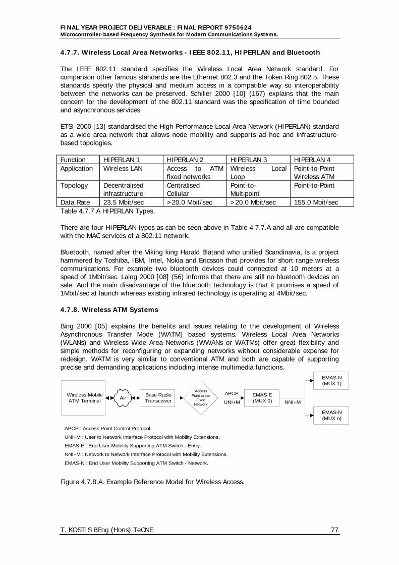
FINAL YEAR PROJECT DELIVERABLE : FINAL REPORT 9750624Microcontroller-based Frequency Synthesis for Modern Communications Systems.
T. KOSTIS BEng (Hons) TeCNE. 77
4.7.7. Wireless Local Area Networks - IEEE 802.11, HIPERLAN and Bluetooth
The IEEE 802.11 standard specifies the Wireless Local Area Network standard. Forcomparison other famous standards are the Ethernet 802.3 and the Token Ring 802.5. Thesestandards specify the physical and medium access in a compatible way so interoperabilitybetween the networks can be preserved. Schiller 2000 [10] (167) explains that the mainconcern for the development of the 802.11 standard was the specification of time boundedand asynchronous services.
ETSI 2000 [13] standardised the High Performance Local Area Network (HIPERLAN) standardas a wide area network that allows node mobility and supports ad hoc and infrastructure-based topologies.
Function HIPERLAN 1 HIPERLAN 2 HIPERLAN 3 HIPERLAN 4Application Wireless LAN Access to ATM
fixed networksWireless LocalLoop
Point-to-PointWireless ATM
Topology Decentralisedinfrastructure
CentralisedCellular
Point-to-Multipoint
Point-to-Point
Data Rate 23.5 Mbit/sec >20.0 Mbit/sec >20.0 Mbit/sec 155.0 Mbit/secTable 4.7.7.A HIPERLAN Types.
There are four HIPERLAN types as can be seen above in Table 4.7.7.A and all are compatiblewith the MAC services of a 802.11 network.
Bluetooth, named after the Viking king Harald Blatand who unified Scandinavia, is a projecthammered by Toshiba, IBM, Intel, Nokia and Ericsson that provides for short range wirelesscommunications. For example two bluetooth devices could connected at 10 meters at aspeed of 1Mbit/sec. Laing 2000 [08] (56) informs that there are still no bluetooth devices onsale. And the main disadvantage of the bluetooth technology is that it promises a speed of1Mbit/sec at launch whereas existing infrared technology is operating at 4Mbit/sec.
4.7.8. Wireless ATM Systems
Bing 2000 [05] explains the benefits and issues relating to the development of WirelessAsynchronous Transfer Mode (WATM) based systems. Wireless Local Area Networks(WLANs) and Wireless Wide Area Networks (WWANs or WATMs) offer great flexibility andsimple methods for reconfiguring or expanding networks without considerable expense forredesign. WATM is very similar to conventional ATM and both are capable of supportingprecise and demanding applications including intense multimedia functions.
Wireless MobileATM Terminal
Base RadioTransceiver
EMAS-E(MUX 0)
AccessPoint to the
FixedNetwork
EMAS-N(MUX n)
EMAS-N(MUX 1)
APCP
UNI+M NNI+MAir
APCP : Access Point Control Protocol.
UNI+M : User to Network Interface Protocol with Mobility Extensions.
NNI+M : Network to Network Interface Protocol with Mobility Extensions.
EMAS-E : End User Mobility Supporting ATM Switch - Entry.
EMAS-N : End User Mobility Supporting ATM Switch - Network.
Figure 4.7.8.A. Example Reference Model for Wireless Access.
FINAL YEAR PROJECT DELIVERABLE : FINAL REPORT 9750624Microcontroller-based Frequency Synthesis for Modern Communications Systems.
T. KOSTIS BEng (Hons) TeCNE. 78
Several changes are needed to make the new ATM model mobility aware. For example datatransfer over the air medium is completely different from its wired counterpart and requiresthe introduction of an addition physical layer called Radio Access Layer (RAL).
MATM Access PointTerminalAdapter
Air EMAS-E EMAS-N ATM SwitchFixed
terminal
Radio Segment Fixed Network Segment
UserProcess
AAL
ATM
PHY
ATM
PHY RAL
ATM
RAL PHY
ATM
RAL PHY
ATM
RAL PHY
ATM
RAL PHY
UserProcess
AAL
ATM
PHYAir
Figure 4.7.8.B. WATM Reference Model and corresponding wireless protocol layers.
The RAL includes the LLC, MAC and Physical layers of the conventional OSI Model.
5. CONCLUSION
The most important mobile radio systems are cellular, cordless and private.
The simple transfer of information from one point to another is not enough. Only beneficialapplications make the channel useful for proper telecommunications. Certain addition andenhancements need to be incorporated to mobile radio systems in order to be able to accessconventional applications like databases and the world wide web from fixed networks. One ofthe most important mobile radio protocols is the Wireless ATM which will allow a seamlessintegration with existing high-bandwidth systems.
FINAL YEAR PROJECT DELIVERABLE : FINAL REPORT 9750624Microcontroller-based Frequency Synthesis for Modern Communications Systems.
T. KOSTIS BEng (Hons) TeCNE. 79
6. BIBLIOGRAPHY & REFERENCES
[01]. BLAKE 1997 Comprehensive Electronic Communication.Minnesota : West Publishing Company. (ISBN 0-314-20140-8)i. Cellular Radio and Personal Communications Systems, (703).ii. Satellite Communications, (642).
[02]. DUNLOP-SMITH 1994 Telecommunications Engineering.London : Chapman & Hall. (ISBN 0-412-56270-7)i. Mobile Communications Systems, (513).ii. Satellite Communications, (493).
[03]. SCHWEBER 1999 Electronic Communications Systems.New Jersey : Simon & Schuster. (ISBN 0-13-780016-9)i. Cellular Telephone and Advanced Wireless Systems, (610).ii. Satellite Communications Navigation and the GPS, (581).
[04]. MILLER 1999 Modern Electronic Communication.New Jersey : Prentice Hall. (ISBN 0-13-927237-2)i. Cellular Telephones, (475).ii. Satellite Communications, (574).
[05]. BING 2000 High-Speed Wireless ATM LANs.London : Artech House. (ISBN 1-58053-092-3)
[06]. GROE-LARSON 2000 CDMA Mobile Radio Design.London : Artech House. (ISBN 1-58053-059-1)
[07]. HALSALL 1996 Data Communications, Computer Networks & Open Systems.London : Artech House. (ISBN 0-201-56506-4)
[08]. LAING 2000 Bluetooth-ache.London : Personal Computer World, April 2000.
[09]. FONTAN 1999 Introduction to Mobile Communications Engineering.London : Artech House. (ISBN 0-89006-391-5)
[10]. SCHILLER 2000 Mobile Communications.London : Addison-Wesley. (ISBN 0-201-39836-2)
[11]. DECT 1999 Website.Geneva : ETSI. (www.dect.ch)
[12] BLUETOOTH 1999 Website.Geneva : Toshiba, IBM, Intel, Nokia, Ericsson. (www.bluetooth.)
[13]. ETSI 1999 Website.Geneva : European Telecommunications Standards Institute. (www.etsi.org)

FINAL YEAR PROJECT DELIVERABLE : FINAL REPORT 9750624Microcontroller-based Frequency Synthesis for Modern Communications Systems.
T. KOSTIS BEng (Hons) TeCNE. 80
9750624
Related Documents