Microarchitectural Wire Management for Performance and Power in Partitioned Architectures * Rajeev Balasubramonian, Naveen Muralimanohar, Karthik Ramani, Venkatanand Venkatachalapathy University of Utah Abstract Future high-performance billion-transistor processors are likely to employ partitioned architectures to achieve high clock speeds, high parallelism, low design complex- ity, and low power. In such architectures, inter-partition communication over global wires has a significant impact on overall processor performance and power consumption. VLSI techniques allow a variety of wire implementations, but these wire properties have previously never been ex- posed to the microarchitecture. This paper advocates global wire management at the microarchitecture level and pro- poses a heterogeneous interconnect that is comprised of wires with varying latency, bandwidth, and energy charac- teristics. We propose and evaluate microarchitectural tech- niques that can exploit such a heterogeneous interconnect to improve performance and reduce energy consumption. These techniques include a novel cache pipeline design, the identification of narrow bit-width operands, the classifica- tion of non-critical data, and the detection of interconnect load imbalance. For a dynamically scheduled partitioned architecture, our results demonstrate that the proposed in- novations result in up to 11% reductions in overall proces- sor ED 2 , compared to a baseline processor that employs a homogeneous interconnect. 1. Introduction One of the biggest challenges for computer architects is the design of billion-transistor architectures that yield high parallelism, high clock speeds, low design complexity, and low power. There appears to be a consensus among several research groups [1, 7, 10, 15, 18, 21, 25, 27, 28, 29, 30, 35, 36, 39, 42] that a partitioned architecture is the best approach to achieving these design goals. Partitioned architectures consist of many small and fast computational units connected by a communication fabric. A computational unit is commonly referred to as a cluster * This work was supported in part by NSF grant CCF-0430063. and is typically comprised of a limited number of ALUs, lo- cal register storage, and a buffer for instruction issue. Since a cluster has limited resources and functionality, it enables fast clocks, low power, and low design effort. Abundant transistor budgets allow the incorporation of many clus- ters on a chip. The instructions of a single program are distributed across the clusters, thereby enabling high par- allelism. Since it is impossible to localize all dependent instructions to a single cluster, data is frequently commu- nicated between clusters over the inter-cluster communica- tion fabric. Depending on the workloads, different flavors of partitioned architectures can exploit instruction-level, data- level, and thread-level parallelism (ILP, DLP, and TLP). As we move to smaller process technologies, logic de- lays scale down with transistor widths, while wire de- lays do not scale down at the same rate. To alleviate the high performance penalty of long wire delays at fu- ture technologies, most research efforts have concentrated on reducing the number of communications through intel- ligent instruction and data assignment to clusters. Such an assignment can be accomplished either at compile-time [21, 27, 30, 35, 36, 39, 42] or at run-time [1, 7, 10, 15, 18]. However, in spite of our best efforts, global communication is here to stay. For a dynamically scheduled 4-cluster sys- tem (described in Sections 4 and 5), performance degrades by 12% when the inter-cluster latency is doubled. The pa- pers listed above also report similar slowdowns for high- latency interconnects. Thus, irrespective of the implemen- tation, partitioned architectures experience a large number of global data transfers and performance can be severely de- graded if the interconnects are not optimized for low delay. Since global communications happen on long wires with high capacitances, they are responsible for a significant fraction of on-chip power dissipation. Interconnect power is a major problem not only in today’s industrial designs, but also in high-performance research prototypes. A recent evaluation by Wang et al. [44] demonstrates that the inter- tile network accounts for 36% of the total energy dissipated in the Raw processor [42]. A recent report by Magen et al. [32] also attributes 50% of total chip power in an Intel processor to interconnects. We are clearly moving to an era Proceedings of the 11th Int’l Symposium on High-Performance Computer Architecture (HPCA-11 2005) 1530-0897/05 $20.00 © 2005 IEEE

Welcome message from author
This document is posted to help you gain knowledge. Please leave a comment to let me know what you think about it! Share it to your friends and learn new things together.
Transcript
Microarchitectural Wire Management for Performance and Power inPartitioned Architectures ∗
Rajeev Balasubramonian, Naveen Muralimanohar, Karthik Ramani, Venkatanand VenkatachalapathyUniversity of Utah
Abstract
Future high-performance billion-transistor processorsare likely to employ partitioned architectures to achievehigh clock speeds, high parallelism, low design complex-ity, and low power. In such architectures, inter-partitioncommunication over global wires has a significant impacton overall processor performance and power consumption.VLSI techniques allow a variety of wire implementations,but these wire properties have previously never been ex-posed to the microarchitecture. This paper advocates globalwire management at the microarchitecture level and pro-poses a heterogeneous interconnect that is comprised ofwires with varying latency, bandwidth, and energy charac-teristics. We propose and evaluate microarchitectural tech-niques that can exploit such a heterogeneous interconnectto improve performance and reduce energy consumption.These techniques include a novel cache pipeline design, theidentification of narrow bit-width operands, the classifica-tion of non-critical data, and the detection of interconnectload imbalance. For a dynamically scheduled partitionedarchitecture, our results demonstrate that the proposed in-novations result in up to 11% reductions in overall proces-sor ED2, compared to a baseline processor that employs ahomogeneous interconnect.
1. Introduction
One of the biggest challenges for computer architects isthe design of billion-transistor architectures that yield highparallelism, high clock speeds, low design complexity, andlow power. There appears to be a consensus among severalresearch groups [1, 7, 10, 15, 18, 21, 25, 27, 28, 29, 30,35, 36, 39, 42] that a partitioned architecture is the bestapproach to achieving these design goals.
Partitioned architectures consist of many small and fastcomputational units connected by a communication fabric.A computational unit is commonly referred to as a cluster
∗This work was supported in part by NSF grant CCF-0430063.
and is typically comprised of a limited number of ALUs, lo-cal register storage, and a buffer for instruction issue. Sincea cluster has limited resources and functionality, it enablesfast clocks, low power, and low design effort. Abundanttransistor budgets allow the incorporation of many clus-ters on a chip. The instructions of a single program aredistributed across the clusters, thereby enabling high par-allelism. Since it is impossible to localize all dependentinstructions to a single cluster, data is frequently commu-nicated between clusters over the inter-cluster communica-tion fabric. Depending on the workloads, different flavors ofpartitioned architectures can exploit instruction-level, data-level, and thread-level parallelism (ILP, DLP, and TLP).
As we move to smaller process technologies, logic de-lays scale down with transistor widths, while wire de-lays do not scale down at the same rate. To alleviatethe high performance penalty of long wire delays at fu-ture technologies, most research efforts have concentratedon reducing the number of communications through intel-ligent instruction and data assignment to clusters. Suchan assignment can be accomplished either at compile-time[21, 27, 30, 35, 36, 39, 42] or at run-time [1, 7, 10, 15, 18].However, in spite of our best efforts, global communicationis here to stay. For a dynamically scheduled 4-cluster sys-tem (described in Sections 4 and 5), performance degradesby 12% when the inter-cluster latency is doubled. The pa-pers listed above also report similar slowdowns for high-latency interconnects. Thus, irrespective of the implemen-tation, partitioned architectures experience a large numberof global data transfers and performance can be severely de-graded if the interconnects are not optimized for low delay.
Since global communications happen on long wires withhigh capacitances, they are responsible for a significantfraction of on-chip power dissipation. Interconnect poweris a major problem not only in today’s industrial designs,but also in high-performance research prototypes. A recentevaluation by Wang et al. [44] demonstrates that the inter-tile network accounts for 36% of the total energy dissipatedin the Raw processor [42]. A recent report by Magen etal. [32] also attributes 50% of total chip power in an Intelprocessor to interconnects. We are clearly moving to an era
Proceedings of the 11th Int’l Symposium on High-Performance Computer Architecture (HPCA-11 2005) 1530-0897/05 $20.00 © 2005 IEEE
where movement of data on a chip can have greater impacton performance and energy than computations involving thedata. In other words, future microprocessors are becomingincreasingly communication-bound.
VLSI techniques enable a variety of different wire im-plementations. For example, by tuning the wire width andspacing, we can design wires with varying latency andbandwidth properties. Similarly, by tuning repeater size andspacing, we can design wires with varying latency and en-ergy properties. Further, as interconnect technology devel-ops, transmission lines may become feasible, enabling verylow latency for very low-bandwidth communication. Datatransfers on the on-chip network also have different require-ments – some transfers benefit from a low latency network,others benefit from a high bandwidth network, and yet oth-ers are latency insensitive. To take advantage of VLSI tech-niques and to better match interconnect design to commu-nication requirements, we propose a heterogeneous inter-connect, where every link consists of wires that are opti-mized for either latency, energy, or bandwidth. We proposenovel mechanisms that can take advantage of these inter-connect choices to improve performance and reduce energyconsumption.
To exploit a low-latency, low-bandwidth interconnect,we design a cache pipeline that employs a subset of theaddress bits to prefetch data out of cache banks. We alsotake advantage of the fact that a number of data transfersinvolve narrow bit-width operands that can benefit from alow-bandwidth interconnect. Further, we can see improvedperformance by diverting bursts of interconnect traffic tohigh-bandwidth high-latency interconnects. These high-bandwidth interconnects can also be designed to be energy-efficient, enabling significant energy savings in addition toperformance improvements.
The paper is organized as follows. Section 2 reviewstechniques that enable different wire implementations. Sec-tion 3 outlines the design of a heterogeneous interconnect.Section 4 describes the proposed innovations to exploit dif-ferent on-chip wires and they are evaluated in Section 5.Finally, Section 6 discusses related work and we concludein Section 7.
2. Wire Implementations with Varying Char-acteristics
The delay of a wire is a function of the RC time constant(R is resistance and C is capacitance). The resistance perunit length of the wire can be expressed by the followingequation [25]:
Rwire =ρ
(thickness − barrier)(width − 2 barrier)(1)
Thickness and width represent the geometrical dimen-sions of the wire cross-section, barrier represents the thinbarrier layer around the wire to prevent copper from dif-fusing into surrounding oxide, and ρ is the material resis-tivity. The capacitance per unit length can be modeled byfour parallel-plate capacitors for each side of the wire and aconstant for fringing capacitance [25]:
Cwire = ε0(2Kεhoriz
thickness
spacing+ 2εvert
width
layerspacing)
+fringe(εhoriz, εvert) (2)
The potentially different relative dielectrics for the verti-cal and horizontal capacitors are represented by εhoriz andεvert, K accounts for Miller-effect coupling capacitances,spacing represents the gap between adjacent wires on thesame metal layer, and layerspacing represents the gap be-tween adjacent metal layers. We now examine the tech-niques that enable wires with varying properties.
Wire Width and Spacing
As can be seen from Equation (1), increasing the widthof the wire can significantly decrease resistivity, while alsoresulting in a modest increase in capacitance per unit length(Equation (2)). Similarly, increasing the spacing betweenadjacent wires results in a drop in Cwire. By allocatingmore metal area per wire and increasing the wire widthand spacing, the overall effect is that the product of Rwire
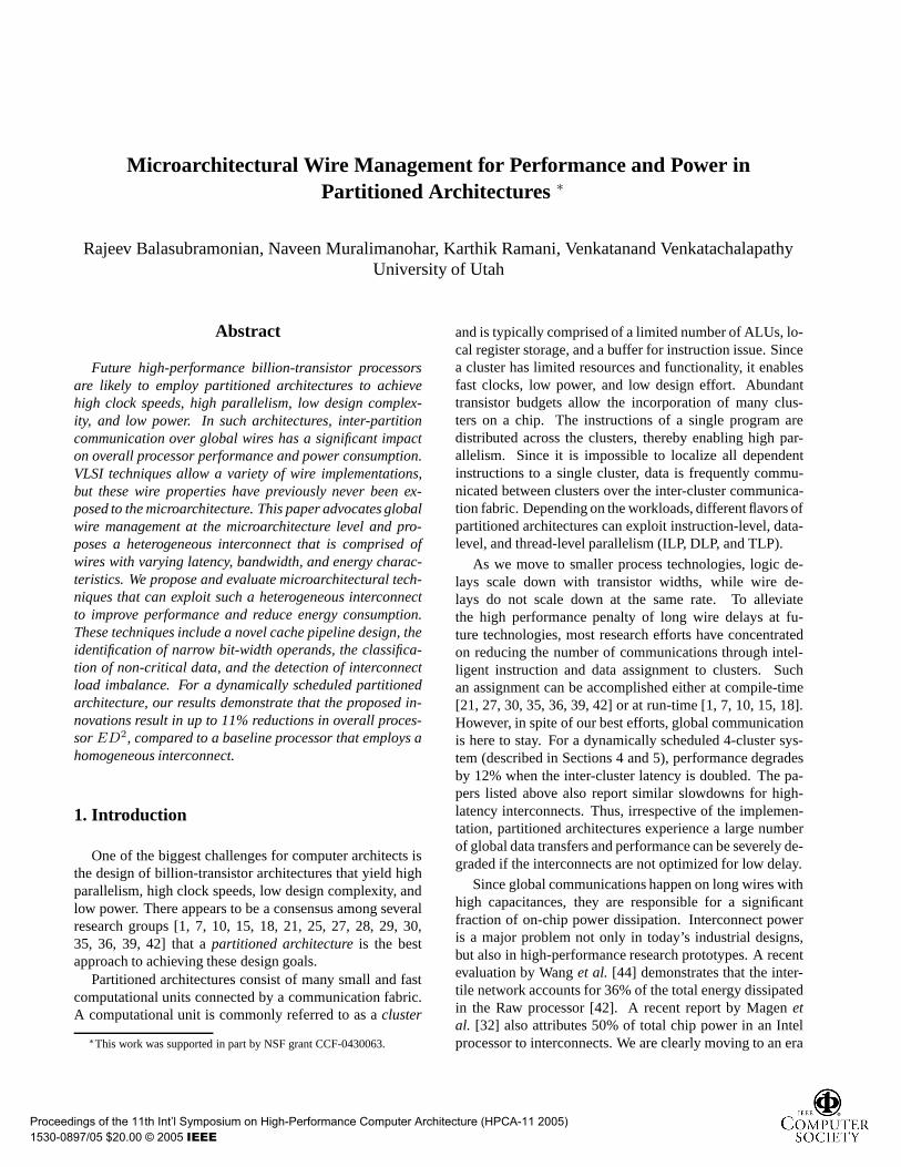
and Cwire decreases, resulting in lower wire delays. Theprimary difference between wires in the different types ofmetal layers in modern processors is the wire width andspacing (in addition to the thickness). Ho et al. [25] re-port that a 10mm unbuffered wire at 180nm technology hasdelays of 57 FO4s, 23 FO4s, and 6 FO4s on local, semi-global, and global wires. Thus, wire width and spacing arepowerful parameters that can vary the latency by at leasta factor of 10. However, wide wires are more suited forlow-bandwidth traffic such as for clock and power distri-bution. If global communication involves the transfer of64-bit data between clusters, employing 64 wide wires canhave enormous area overheads. For a given metal area, thewider the wire, the fewer the number of wires that can be ac-commodated (see Figure 1). Hence, optimizing a wire forlow delay by designing wide wires has a negative impact onbandwidth.
Repeater Size and Spacing
The resistance and capacitance of a wire are both lin-ear functions of the wire length. Hence, the delay of awire, that depends on the product of wire resistance andcapacitance, is a quadratic function of wire length. A sim-ple technique to overcome this quadratic dependence is tobreak the wire into multiple smaller segments and connectthem with repeaters [5]. As a result, wire delay becomes a
Proceedings of the 11th Int’l Symposium on High-Performance Computer Architecture (HPCA-11 2005) 1530-0897/05 $20.00 © 2005 IEEE
Delay Optimized Bandwidth Optimized Power Optimized Power and Bandwidth Optimized
Figure 1. Examples of different wire implementations. Energy optimized wires have fewer and smaller re-peaters, while bandwidth optimized wires have narrow widths and spacing.
linear function of wire length and depends on the numberof segments, the wire delay across each segment, and thelogic delay across each repeater. Overall wire delay can beminimized by selecting optimal repeater sizes and spacingbetween repeaters [5] and this technique is commonly em-ployed in modern-day processors. However, these repeatershave high overheads associated with them. Contacts haveto be cut from the metal layer to the silicon substrate ev-ery time a logic element is introduced in the middle of awire. The contacts and the transistors not only impose areaoverheads and routing constraints, but also impose high ca-pacitive loads on the wires. Banerjee et al. [8, 9] report thatsub-100nm designs will have over a million repeaters andthat optimally sized repeaters are approximately 450 timesthe minimum sized inverter at that technology point.
Energy in the interconnect can be reduced by employingrepeaters that are smaller than the optimally-sized repeatersand by increasing the spacing between successive repeaters(see Figure 1). This increases overall wire delay. Recently,Banerjee et al. [8] developed a methodology to estimate re-peater size and spacing that minimizes power consumptionfor a fixed wire delay. They show that at 50nm technol-ogy, it is possible to design a repeater configuration suchthat the wire has twice the delay and 1/5th the energy of awire that is delay-optimal. Thus, repeater size and spacingare parameters that can dramatically influence interconnectpower and performance.
Transmission Lines
In future technologies, other promising wire implemen-tations may become feasible, such as transmission lines [16,19]. In a transmission line, the wire delay is determined bythe time taken to detect a voltage ripple on the wire. Thisdelay is determined by the LC time constant and the veloc-ity of the ripple, which is a function of the speed of lightin the dielectric surrounding the interconnect. A transmis-sion line, therefore, enables very low wire latencies. Fora wire to operate as a transmission line, it must have veryhigh width, thickness, horizontal and vertical spacing, andsignal frequency. There are other implementation issues aswell, such as the design of signal modulation and sensing
circuits, reference planes above and below the metal layer,and shielding power and ground lines adjacent to each trans-mission line [12].
Because of the large area requirements and other asso-ciated costs, transmission lines have been sparsely used inmodern processors, usually as single wires for clock distri-bution [33, 45, 46]. They have also been shown to workin other test CMOS chips [16, 20]. As we move to higherclock frequencies and increasing metal layers, transmissionline implementations may become more practical and cost-effective. However, owing to the high area requirementsper wire, transmission lines are likely to be feasible onlyfor very low bandwidth communication. Thus, a transmis-sion line represents another interesting wire implementationthat trades off bandwidth for extremely low latencies.
3. Heterogeneous Interconnects
From the above discussion, it is clear that a large num-ber of different wire implementations are possible, either byvarying properties such as wire width/spacing and repeatersize/spacing, or by employing transmission lines. Typically,inter-cluster global interconnects are designed to minimizedelay for the transfer of 64-bit data and the associated tags(typically fewer than eight bits). Wire widths are chosensuch that 72 wires can be accommodated in the availablemetal area and repeaters are sized and spaced to optimizedelay. We refer to these wires as B-Wires. In addition tothis base 72-bit interconnect, there are at least three otherinteresting wire implementations that the architecture canbenefit from:
• P-Wires: Wires that are power-optimal. The wireshave longer delays as they employ small repeater sizesand wide repeater spacing.
• W-Wires: Wires that are bandwidth-optimal. The wireshave minimum width and spacing and have longer de-lays.
• L-Wires: Wires that are latency-optimal. These wiresoperate as transmission lines or employ very wide
Proceedings of the 11th Int’l Symposium on High-Performance Computer Architecture (HPCA-11 2005) 1530-0897/05 $20.00 © 2005 IEEE
width and spacing and have low bandwidth (poten-tially, a network with fewer than 20 bits).
To limit the range of possibilities, P-Wires and W-Wires canbe combined to form a single wire implementation withminimum width and spacing and with small repeater sizesand wide repeater spacing. Such wires have poor delaycharacteristics, but allow low power and high bandwidth(referred to as PW-Wires).
These options can be incorporated into the inter-clusterglobal interconnect in a variety of ways. In this evaluation,we limit ourselves to the following topology. Every link onthe network offers the same degree of heterogeneity. For ex-ample, every link may consist of 72 B-Wires, 144 PW-Wires,and 18 L-Wires. Thus, for any data transfer, the microar-chitecture can dynamically choose to effect the transfer oneither B-Wires, PW-Wires, or L-Wires. Such an implemen-tation choice may entail additional complexity within thesend buffers. To reduce this complexity, one can design atopology where some links consist entirely of PW-Wires,while others consist entirely of B-Wires. Such a topologyhas lower design complexity, but affords less flexibility tothe microarchitecture. In this paper, we adopt the formerimplementation since we are evaluating the potential of aheterogeneous interconnect. We argue that the additionallogic to route data to one of three possible interconnectsonly requires one-to-three demultiplexers and compared toa base processor that already has multiple interconnects, theoverhead is likely to be negligible. We assume a modelwhere in any cycle, data can be dynamically assigned toone of the available wire implementations based on the pro-gram’s needs. The mechanisms that enable this dynamicdecision-making are discussed in the next section.
Different wire implementations may or may not be ac-commodated on a single metal layer. There are no techno-logical barriers to having wires with different width/spacingor repeater size/spacing on a single metal layer. However,aspect ratio guidelines necessitate that wire width can not bereduced beyond a certain limit. If the width and spacing forW-Wires or PW-Wires is lower than this limit, they may haveto be implemented on a lower metal layer that has smallerthickness. Further, current implementations of transmissionlines are rather cumbersome and entail huge overheads. Un-less these implementations become more cost-effective, theuse of transmission lines will involve additional metal lay-ers. The International Technology Roadmap for Semicon-ductors [3] projects that the number of metal layers will in-crease in future generations. Evaluations of this nature helpidentify the most promising ways to exploit such a resource.
4. Exploiting Heterogeneous Interconnects
In this section, we describe the partitioned architecturemodel that serves as an evaluation platform for this study
and the proposed innovations that can take advantage of aheterogeneous interconnect.
The Baseline Partitioned Architecture
Instruction assignment to clusters in a partitioned archi-tecture may happen at compile-time [11, 21, 27, 30, 35,36, 39], or at run-time [1, 7, 10, 15, 18]. There are ad-vantages to either approach – static techniques entail lowerhardware overheads and have access to more informationon program dataflow, while dynamic techniques are morereactive to events such as branch mispredicts, cache misses,network congestion, etc. Our evaluations employ a dynami-cally scheduled partitioned architecture. We expect that ourproposals can be applied even to statically scheduled archi-tectures.
Our partitioned architecture model dispatches a largewindow of in-flight instructions from a single-threadedapplication. We adopt a centralized cache implementa-tion because earlier studies have shown that a central-ized cache offers nearly as much performance as a dis-tributed cache while enabling low implementation complex-ity [6, 23, 38]. The assignment of instructions to clus-ters happens through a state-of-the-art dynamic instructionsteering heuristic [7, 15, 43] that takes the following infor-mation into account: data dependences, cluster load im-balance, criticality of operands, and proximity to the datacache. While dispatching an instruction, the steering algo-rithm assigns weights to each cluster to determine the clus-ter that is most likely to minimize communication and issue-related stalls. Weights are assigned to a cluster if it producesinput operands for the instruction and if it has many emptyissue queue entries. Additional weights are assigned to acluster if it is the producer of the input operand that is pre-dicted to be on the critical path for the instruction’s execu-tion. For loads, more weights are assigned to clusters thatare closest to the data cache. The steering algorithm assignsthe instruction to the cluster that has the most weights. Ifthat cluster has no free register and issue queue resources,the instruction is assigned to the nearest cluster with avail-able resources.
Results produced within a cluster are bypassed to con-sumers in that cluster in the same cycle, while communi-cating the result to consumers in other clusters takes ad-ditional cycles. In order to effect the transfer of data be-tween clusters, the instruction decode and rename stage in-serts a “copy instruction” [15] in the producing cluster thatplaces the value on the inter-cluster network as soon as thevalue is made available. Each cluster has a scheduler for theinter-cluster network that is similar in organization to theissue queue and that has an issue bandwidth that matchesthe maximum number of transfers possible on each link ofthe network. Similar to the instruction wake-up process inconventional dynamic superscalars, the register tags for theoperand are sent on the network ahead of the data so that the
Proceedings of the 11th Int’l Symposium on High-Performance Computer Architecture (HPCA-11 2005) 1530-0897/05 $20.00 © 2005 IEEE

L1 D
Crossbar
Cluster
B−WireL−WirePW−Wire
L1 D
Crossbar
Ring
(a) 4−cluster system with heterogeneous wires
(b) 16−cluster system withhierarchical interconnect
Figure 2. (a) A partitioned architecture model with4 clusters and a heterogeneous interconnect com-prised of B-, L-, and PW-Wires. (b) A 16-clustersystem with a hierarchical interconnect. Sets offour clusters are connected with a crossbar andthe crossbars are connected in a ring topology.
dependent instruction can be woken up and can consume thevalue as soon as it arrives.
For most of our experiments, we assume a processormodel that has four clusters. These four clusters and thecentralized data cache are connected through a crossbar net-work, as shown in Figure 2 (a). All links contain a uni-directional interconnect in each direction. The processormodel in Figure 2 (a) adopts a heterogeneous interconnectwhere every link in the network is comprised of B-Wires,PW-Wires, and L-Wires. Note that every data transfer hasthe option to use any one of these sets of wires. Our eval-uations show the effects of using interconnects that employdifferent combinations of these sets of wires. For all proces-sor organizations, the bandwidth requirements to the cacheare much higher than bandwidth requirements to the clus-ters since more than one third of all instructions are loads orstores. Hence, the links going in and out of the cache are as-sumed to have twice as much area and twice as many wiresas the links going in and out of a cluster. If multiple trans-fers compete for a link in a cycle, one transfer is effectedin that cycle, while the others are buffered. We assume un-bounded buffers at each node of the network. An earlierstudy [37] has shown that these buffers typically require amodest number of entries. We also examine aggressive pro-cessor models with 16 clusters. For a 16-cluster system, weadopt a hierarchical topology similar to the one proposed byAggarwal and Franklin [2]. As shown in Figure 2 (b), a setof four clusters is connected through a crossbar, allowinglow-latency communication to neighboring clusters. Thecrossbars are connected with a ring topology. Similar to the4-cluster system, every link in the network is comprised of
wires with different properties.
Accelerating Cache Access
First, we examine how low-latency low-bandwidth L-Wires can be exploited to improve performance. L-Wiresare designed by either employing very large wire widths andspacing or by implementing transmission lines. Because ofthe area overhead, for the sake of this discussion, we assumethat 18 L-Wires occupy the same metal area as 72 B-Wires.
Consider the behavior of the cache pipeline in the base-line processor. When a cluster executes a load instruc-tion, it computes the effective address and communicatesit to the centralized load/store queue (LSQ) and cache. Theload/store queue waits until it receives addresses of storesprior to the load in program order, guarantees that there isno memory dependence, and then initiates the cache access.The cost of communication to the cache influences load la-tency in two ways – (i) it delays the arrival of load addressesat the LSQ, (ii) it delays the arrival of store addresses atthe LSQ, thereby delaying the resolution of memory depen-dences.
To accelerate cache access, we propose the followingnovel technique. A subset of the address bits are trans-mitted on low-latency L-Wires to prefetch data out of theL1 cache and hide the high communication cost of trans-mitting the entire address. After the cluster computes theeffective address, the least significant (LS) bits of the ad-dress are transmitted on the low-latency L-Wires, while themost significant (MS) bits are transmitted on B-Wires. Thesame happens for store addresses. Thus, the LSQ quicklyreceives the LS bits for loads and stores, while the MS bitstake much longer. The early arrival of the partial addressesallows the following optimizations.
The LSQ can effect a partial comparison of load andstore addresses with the available LS bits. If the LS bitsof the load do not match the LS bits of any earlier store,the load is guaranteed to not have any memory dependenceconflicts and it can begin cache access. If the LS bits ofthe load match the LS bits of an earlier store, it has to waitfor the MS bits to arrive before determining if there is atrue dependence. A large number of false dependences canalso increase contention for the LSQ ports. Fortunately, wefound that false dependences were encountered for fewerthan 9% of all loads when employing eight LS bits for thepartial address comparison.
To effect an L1 data cache access, the least significantbits of the effective address are used to index into the dataand tag RAM arrays and read out a relevant set of cacheblocks. The most significant bits of the effective addressare used to index into the TLB and the resulting translationis then compared with the tags to select the appropriate datablock and forward it to the cluster. Since the accesses to thecache RAM arrays do not require the most significant bits,the accesses can be initiated as soon as the least significant
Proceedings of the 11th Int’l Symposium on High-Performance Computer Architecture (HPCA-11 2005) 1530-0897/05 $20.00 © 2005 IEEE
bits of the address arrive on L-Wires (provided the L-Wirestransmit enough bits to determine the set index).
Similarly, a few bits of the virtual page number can beincluded in the transfer on the L-Wires. This allows TLBaccess to proceed in parallel with RAM array look-up. Themodifications to enable indexing with partial address in-formation are more significant for a CAM structure thana RAM structure. Hence, a highly-associative TLB de-sign may be more amenable to this modified pipeline than afully-associative one. When the rest of the effective addressarrives, tag comparison selects the correct translation froma small subset of candidate translations.
Thus, the transfer of partial address bits on L-Wires en-ables data to be prefetched out of L1 cache and TLB banksand hide the RAM access latency, which is the biggest com-ponent in cache access time. If the cache RAM access hascompleted by the time the entire address arrives, only an ad-ditional cycle is spent to detect the correct TLB translationand effect the tag comparison before returning data to thecluster. This overlap of effective address transfer with cacheRAM and TLB access can result in a reduction in effectiveload latency if the latency difference between L-Wires andB-Wires is significant.
It must be noted that the proposed pipeline works welland yields speedups even if the processor implements someform of memory dependence speculation. The partial ad-dress can proceed straight to the L1 cache and prefetch dataout of cache banks without going through partial addresscomparisons in the LSQ if it is predicted to not have mem-ory dependences. To allow cache and TLB index bits to fitin a narrow low-bandwidth interconnect, it might be neces-sary to make the cache and TLB highly set-associative. Forexample, 18 L-Wires can accommodate 6 bits of tag to iden-tify the instruction in the LSQ, 8 index bits for the L1 datacache, and 4 index bits for the TLB. For the assumed cacheand TLB sizes, this corresponds to an associativity of 4 and8 for the cache and TLB, respectively. If the associativity isreduced, we may need a few more L-Wires.
Narrow Bit-Width Operands
An interconnect composed of L-Wires can also be em-ployed for results that can be encoded by a few bits. 18L-Wires can accommodate eight bits of register tag and tenbits of data. We employ the simplest form of data com-paction here – integer results between 0 and 1023 are eligi-ble for transfer on L-Wires. The hardware required to detectnarrow bit-width data can be easily implemented – the Pow-erPC 603 [22] has hardware to detect the number of leadingzeros that is then used to determine the latency for integermultiply. A special case in the transfer of narrow bit-widthdata is the communication of a branch mispredict back tothe front-end. This only involves the branch ID that canbe easily accommodated on L-Wires, thereby reducing thebranch mispredict penalty.
Other forms of data compaction might also be possible,but is not explored here. For example, Yang et al. [47] iden-tify that the eight most frequent values in SPEC95-Int pro-grams account for roughly 50% of all data cache accessesand can be easily encoded by a few bits.
In order to schedule a wake-up operation at the consum-ing cluster, the register tags are sent before the data itself.For a narrow bit-width operand, the tags have to be sent onL-Wires. Hence, the pipeline requires advance knowledgeof whether the result can be expressed in 10 bits. For ourevaluations, we make the optimistic assumption that this in-formation is available early in the pipeline. A realistic im-plementation would require inspection of the instruction’sinput operands or a simple predictor. We confirmed thata predictor with 8K 2-bit saturating counters, that predictsthe occurrence of a narrow bit-width result when the 2-bitcounter value is three, is able to identify 95% of all narrowbit-width results. With such a high-confidence predictor,only 2% of all results predicted to be narrow have bit widthsgreater than 10.
Exploiting PW-Wires
Next, we examine how PW-Wires can be employed tonot only reduce contention in other wires, but also reduceenergy consumption. Our objective here is to identify thosedata transfers that can tolerate the higher latency of thesewires or to identify situations when the cost of contention onB-Wires offsets its wire latency advantage. If a data transferhas the choice of using either B-Wires or PW-Wires, the fol-lowing three criteria dictate when a transfer can be effectedon the high bandwidth, low energy, high latency PW-Wires:
• If the input operands are already ready in a remote reg-ister file at the time an instruction is dispatched, theoperands are transferred to the instruction’s cluster onPW-Wires. The rationale here is that there is usually along gap between instruction dispatch and issue andthe long communication latency for the ready inputoperand can be tolerated.
• Store data is assigned to PW-Wires. This can slow theprogram down only if the store is holding up the com-mit process or if there is a waiting dependent load.Both are fairly rare cases and we noticed a minimalperformance impact from adopting this policy.
• We keep track of the amount of traffic injected into ei-ther interconnect in the past N cycles (N=5 in our sim-ulations). If the difference between the traffic in eachinterconnect exceeds a certain pre-specified threshold(10 in our simulations), subsequent data transfers aresteered to the less congested interconnect.
Thus, by steering non-critical data towards the high-bandwidth energy-efficient interconnect, we are likely tosee little performance degradation and by steering dataaway from the congested interconnect, we can potentially
Proceedings of the 11th Int’l Symposium on High-Performance Computer Architecture (HPCA-11 2005) 1530-0897/05 $20.00 © 2005 IEEE
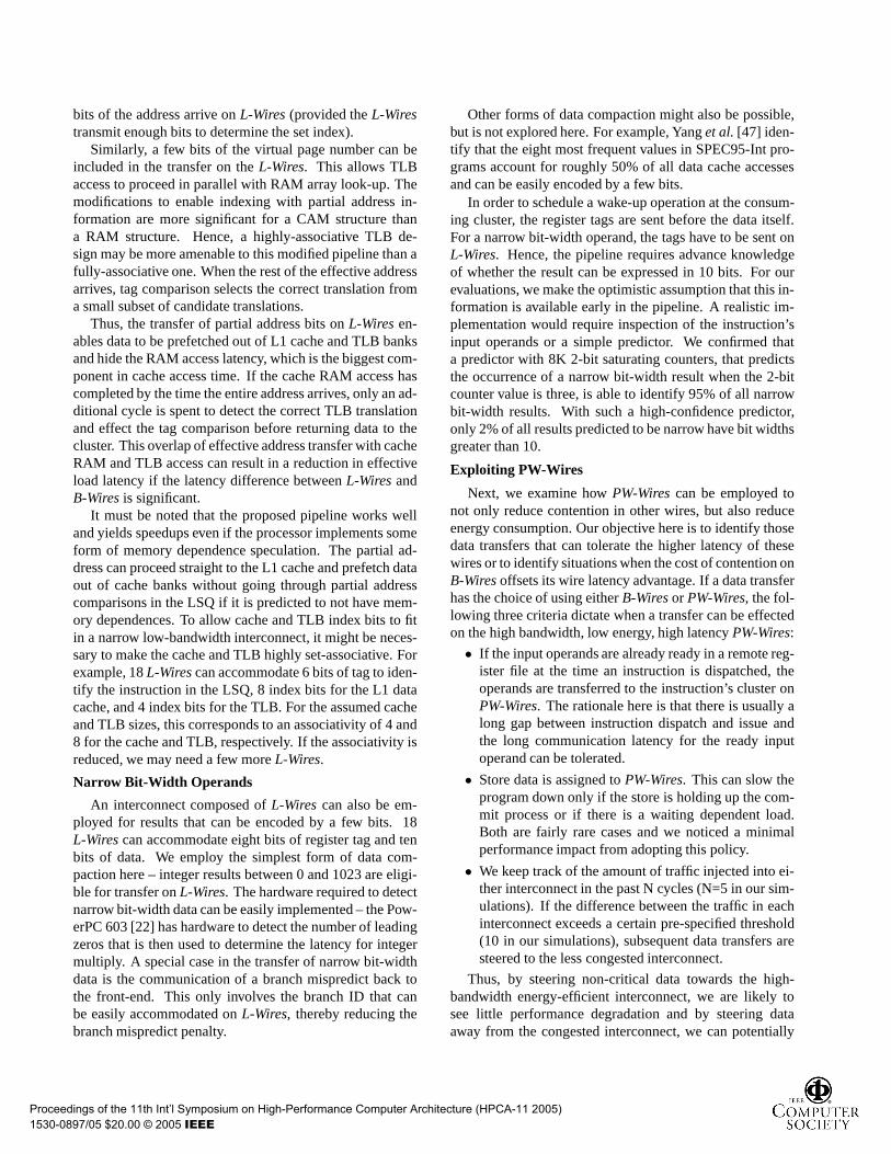
Fetch queue size 64 Branch predictor comb. of bimodal and 2-levelBimodal predictor size 16K Level 1 predictor 16K entries, history 12
Level 2 predictor 16K entries BTB size 16K sets, 2-wayBranch mispredict penalty at least 12 cycles Fetch width 8 (across up to 2 basic blocks)
Issue queue size 15 per cluster (int and fp, each) Register file size 32 per cluster (int and fp, each)Integer ALUs/mult-div 1/1 per cluster FP ALUs/mult-div 1/1 per cluster
L1 I-cache 32KB 2-way Memory latency 300 cycles for the first blockL1 D-cache 32KB 4-way set-associative, L2 unified cache 8MB 8-way, 30 cycles
6 cycles, 4-way word-interleaved I and D TLB 128 entries, 8KB page size
Table 1. Simplescalar simulator parameters.
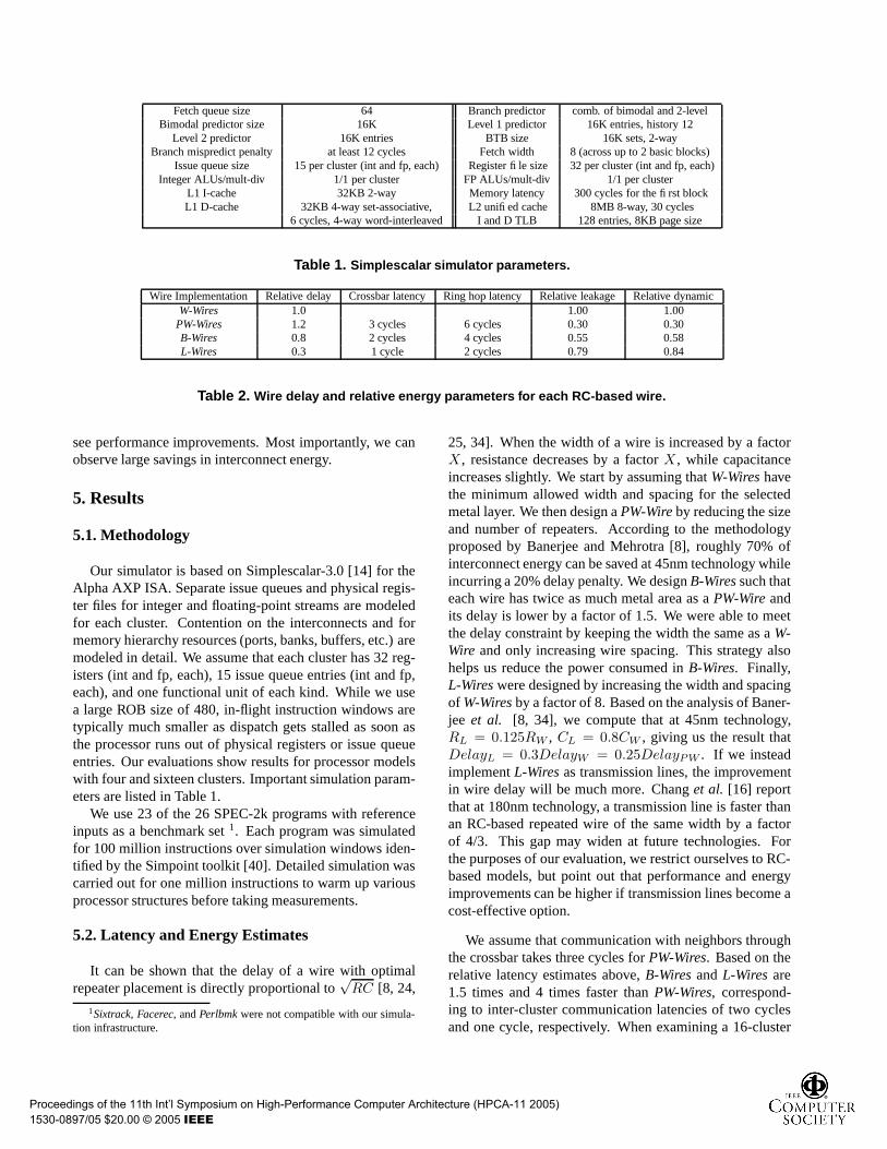
Wire Implementation Relative delay Crossbar latency Ring hop latency Relative leakage Relative dynamicW-Wires 1.0 1.00 1.00
PW-Wires 1.2 3 cycles 6 cycles 0.30 0.30B-Wires 0.8 2 cycles 4 cycles 0.55 0.58L-Wires 0.3 1 cycle 2 cycles 0.79 0.84
Table 2. Wire delay and relative energy parameters for each RC-based wire.
see performance improvements. Most importantly, we canobserve large savings in interconnect energy.
5. Results
5.1. Methodology
Our simulator is based on Simplescalar-3.0 [14] for theAlpha AXP ISA. Separate issue queues and physical regis-ter files for integer and floating-point streams are modeledfor each cluster. Contention on the interconnects and formemory hierarchy resources (ports, banks, buffers, etc.) aremodeled in detail. We assume that each cluster has 32 reg-isters (int and fp, each), 15 issue queue entries (int and fp,each), and one functional unit of each kind. While we usea large ROB size of 480, in-flight instruction windows aretypically much smaller as dispatch gets stalled as soon asthe processor runs out of physical registers or issue queueentries. Our evaluations show results for processor modelswith four and sixteen clusters. Important simulation param-eters are listed in Table 1.
We use 23 of the 26 SPEC-2k programs with referenceinputs as a benchmark set 1. Each program was simulatedfor 100 million instructions over simulation windows iden-tified by the Simpoint toolkit [40]. Detailed simulation wascarried out for one million instructions to warm up variousprocessor structures before taking measurements.
5.2. Latency and Energy Estimates
It can be shown that the delay of a wire with optimalrepeater placement is directly proportional to
√RC [8, 24,
1Sixtrack, Facerec, and Perlbmk were not compatible with our simula-tion infrastructure.
25, 34]. When the width of a wire is increased by a factorX , resistance decreases by a factor X , while capacitanceincreases slightly. We start by assuming that W-Wires havethe minimum allowed width and spacing for the selectedmetal layer. We then design a PW-Wire by reducing the sizeand number of repeaters. According to the methodologyproposed by Banerjee and Mehrotra [8], roughly 70% ofinterconnect energy can be saved at 45nm technology whileincurring a 20% delay penalty. We design B-Wires such thateach wire has twice as much metal area as a PW-Wire andits delay is lower by a factor of 1.5. We were able to meetthe delay constraint by keeping the width the same as a W-Wire and only increasing wire spacing. This strategy alsohelps us reduce the power consumed in B-Wires. Finally,L-Wires were designed by increasing the width and spacingof W-Wires by a factor of 8. Based on the analysis of Baner-jee et al. [8, 34], we compute that at 45nm technology,RL = 0.125RW , CL = 0.8CW , giving us the result thatDelayL = 0.3DelayW = 0.25DelayPW . If we insteadimplement L-Wires as transmission lines, the improvementin wire delay will be much more. Chang et al. [16] reportthat at 180nm technology, a transmission line is faster thanan RC-based repeated wire of the same width by a factorof 4/3. This gap may widen at future technologies. Forthe purposes of our evaluation, we restrict ourselves to RC-based models, but point out that performance and energyimprovements can be higher if transmission lines become acost-effective option.
We assume that communication with neighbors throughthe crossbar takes three cycles for PW-Wires. Based on therelative latency estimates above, B-Wires and L-Wires are1.5 times and 4 times faster than PW-Wires, correspond-ing to inter-cluster communication latencies of two cyclesand one cycle, respectively. When examining a 16-cluster
Proceedings of the 11th Int’l Symposium on High-Performance Computer Architecture (HPCA-11 2005) 1530-0897/05 $20.00 © 2005 IEEE
0
0.5
1
1.5
2
2.5
ammpapplu
apsi artbzip2
crafty eon
equakefm
a3dgalgel
gap gccgzip
lucasmcf
mesamgrid
parserswim twolf
vortex vpr
wupwise AM
IPC
Baseline: 144 B-Wires
Low-latency optimizations: 144B-Wires and 36 L-Wires
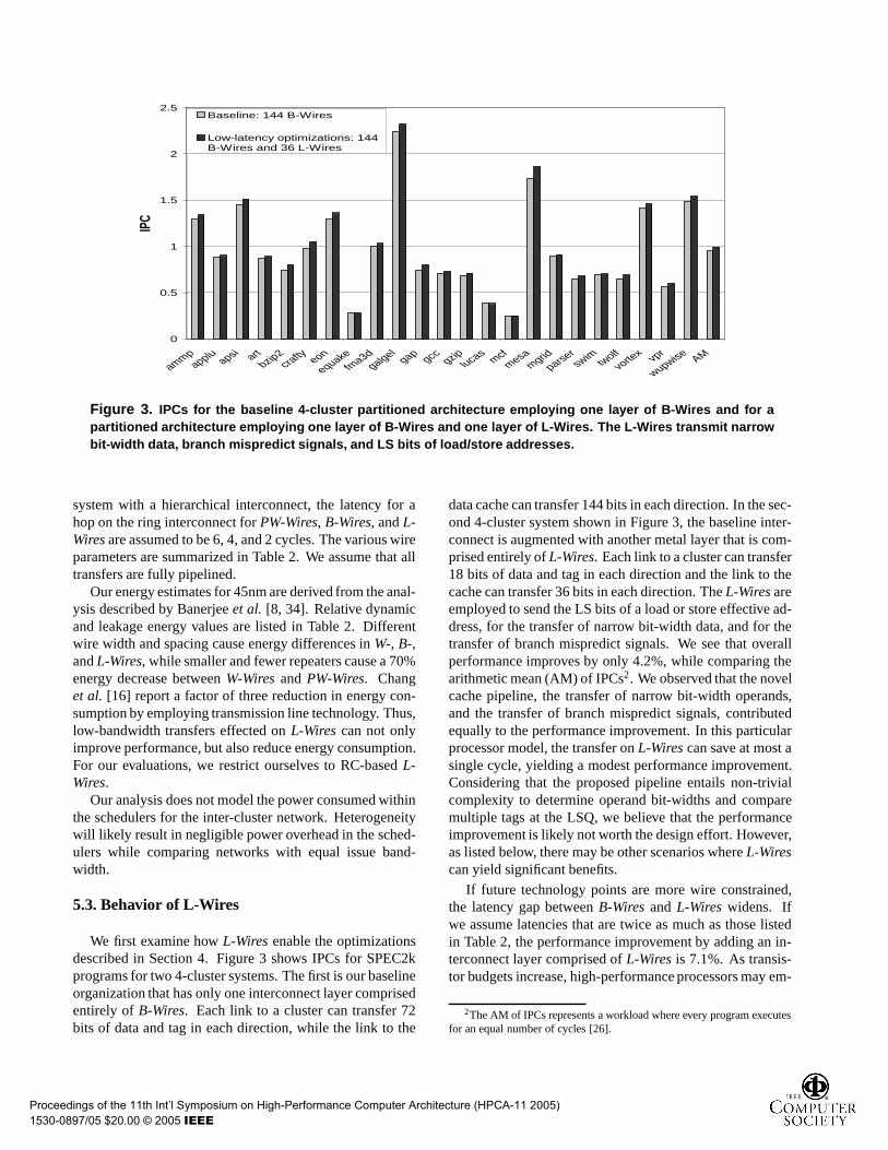
Figure 3. IPCs for the baseline 4-cluster partitioned architecture employing one layer of B-Wires and for apartitioned architecture employing one layer of B-Wires and one layer of L-Wires. The L-Wires transmit narrowbit-width data, branch mispredict signals, and LS bits of load/store addresses.
system with a hierarchical interconnect, the latency for ahop on the ring interconnect for PW-Wires, B-Wires, and L-Wires are assumed to be 6, 4, and 2 cycles. The various wireparameters are summarized in Table 2. We assume that alltransfers are fully pipelined.
Our energy estimates for 45nm are derived from the anal-ysis described by Banerjee et al. [8, 34]. Relative dynamicand leakage energy values are listed in Table 2. Differentwire width and spacing cause energy differences in W-, B-,and L-Wires, while smaller and fewer repeaters cause a 70%energy decrease between W-Wires and PW-Wires. Changet al. [16] report a factor of three reduction in energy con-sumption by employing transmission line technology. Thus,low-bandwidth transfers effected on L-Wires can not onlyimprove performance, but also reduce energy consumption.For our evaluations, we restrict ourselves to RC-based L-Wires.
Our analysis does not model the power consumed withinthe schedulers for the inter-cluster network. Heterogeneitywill likely result in negligible power overhead in the sched-ulers while comparing networks with equal issue band-width.
5.3. Behavior of L-Wires
We first examine how L-Wires enable the optimizationsdescribed in Section 4. Figure 3 shows IPCs for SPEC2kprograms for two 4-cluster systems. The first is our baselineorganization that has only one interconnect layer comprisedentirely of B-Wires. Each link to a cluster can transfer 72bits of data and tag in each direction, while the link to the
data cache can transfer 144 bits in each direction. In the sec-ond 4-cluster system shown in Figure 3, the baseline inter-connect is augmented with another metal layer that is com-prised entirely of L-Wires. Each link to a cluster can transfer18 bits of data and tag in each direction and the link to thecache can transfer 36 bits in each direction. The L-Wires areemployed to send the LS bits of a load or store effective ad-dress, for the transfer of narrow bit-width data, and for thetransfer of branch mispredict signals. We see that overallperformance improves by only 4.2%, while comparing thearithmetic mean (AM) of IPCs2. We observed that the novelcache pipeline, the transfer of narrow bit-width operands,and the transfer of branch mispredict signals, contributedequally to the performance improvement. In this particularprocessor model, the transfer on L-Wires can save at most asingle cycle, yielding a modest performance improvement.Considering that the proposed pipeline entails non-trivialcomplexity to determine operand bit-widths and comparemultiple tags at the LSQ, we believe that the performanceimprovement is likely not worth the design effort. However,as listed below, there may be other scenarios where L-Wirescan yield significant benefits.
If future technology points are more wire constrained,the latency gap between B-Wires and L-Wires widens. Ifwe assume latencies that are twice as much as those listedin Table 2, the performance improvement by adding an in-terconnect layer comprised of L-Wires is 7.1%. As transis-tor budgets increase, high-performance processors may em-
2The AM of IPCs represents a workload where every program executesfor an equal number of cycles [26].
Proceedings of the 11th Int’l Symposium on High-Performance Computer Architecture (HPCA-11 2005) 1530-0897/05 $20.00 © 2005 IEEE
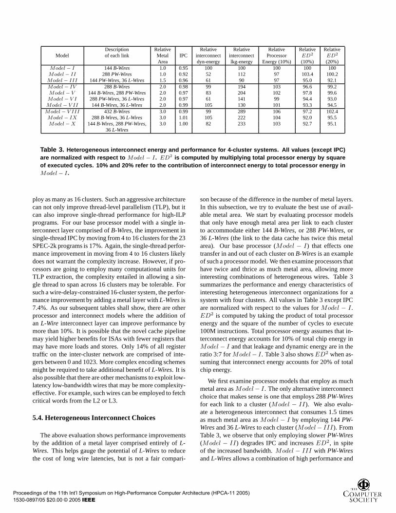
Description Relative Relative Relative Relative Relative RelativeModel of each link Metal IPC interconnect interconnect Processor ED
2ED
2
Area dyn-energy lkg-energy Energy (10%) (10%) (20%)Model − I 144 B-Wires 1.0 0.95 100 100 100 100 100Model− II 288 PW-Wires 1.0 0.92 52 112 97 103.4 100.2Model− III 144 PW-Wires, 36 L-Wires 1.5 0.96 61 90 97 95.0 92.1Model − IV 288 B-Wires 2.0 0.98 99 194 103 96.6 99.2Model − V 144 B-Wires, 288 PW-Wires 2.0 0.97 83 204 102 97.8 99.6Model − V I 288 PW-Wires, 36 L-Wires 2.0 0.97 61 141 99 94.4 93.0Model − V II 144 B-Wires, 36 L-Wires 2.0 0.99 105 130 101 93.3 94.5Model − V III 432 B-Wires 3.0 0.99 99 289 106 97.2 102.4Model− IX 288 B-Wires, 36 L-Wires 3.0 1.01 105 222 104 92.0 95.5Model−X 144 B-Wires, 288 PW-Wires, 3.0 1.00 82 233 103 92.7 95.1
36 L-Wires
Table 3. Heterogeneous interconnect energy and performance for 4-cluster systems. All values (except IPC)are normalized with respect to Model − I. ED
2 is computed by multiplying total processor energy by squareof executed cycles. 10% and 20% refer to the contribution of interconnect energy to total processor energy inModel − I.
ploy as many as 16 clusters. Such an aggressive architecturecan not only improve thread-level parallelism (TLP), but itcan also improve single-thread performance for high-ILPprograms. For our base processor model with a single in-terconnect layer comprised of B-Wires, the improvement insingle-thread IPC by moving from 4 to 16 clusters for the 23SPEC-2k programs is 17%. Again, the single-thread perfor-mance improvement in moving from 4 to 16 clusters likelydoes not warrant the complexity increase. However, if pro-cessors are going to employ many computational units forTLP extraction, the complexity entailed in allowing a sin-gle thread to span across 16 clusters may be tolerable. Forsuch a wire-delay-constrained 16-cluster system, the perfor-mance improvement by adding a metal layer with L-Wires is7.4%. As our subsequent tables shall show, there are otherprocessor and interconnect models where the addition ofan L-Wire interconnect layer can improve performance bymore than 10%. It is possible that the novel cache pipelinemay yield higher benefits for ISAs with fewer registers thatmay have more loads and stores. Only 14% of all registertraffic on the inter-cluster network are comprised of inte-gers between 0 and 1023. More complex encoding schemesmight be required to take additional benefit of L-Wires. It isalso possible that there are other mechanisms to exploit low-latency low-bandwidth wires that may be more complexity-effective. For example, such wires can be employed to fetchcritical words from the L2 or L3.
5.4. Heterogeneous Interconnect Choices
The above evaluation shows performance improvementsby the addition of a metal layer comprised entirely of L-Wires. This helps gauge the potential of L-Wires to reducethe cost of long wire latencies, but is not a fair compari-
son because of the difference in the number of metal layers.In this subsection, we try to evaluate the best use of avail-able metal area. We start by evaluating processor modelsthat only have enough metal area per link to each clusterto accommodate either 144 B-Wires, or 288 PW-Wires, or36 L-Wires (the link to the data cache has twice this metalarea). Our base processor (Model − I) that effects onetransfer in and out of each cluster on B-Wires is an exampleof such a processor model. We then examine processors thathave twice and thrice as much metal area, allowing moreinteresting combinations of heterogeneous wires. Table 3summarizes the performance and energy characteristics ofinteresting heterogeneous interconnect organizations for asystem with four clusters. All values in Table 3 except IPCare normalized with respect to the values for Model − I .ED2 is computed by taking the product of total processorenergy and the square of the number of cycles to execute100M instructions. Total processor energy assumes that in-terconnect energy accounts for 10% of total chip energy inModel − I and that leakage and dynamic energy are in theratio 3:7 for Model− I . Table 3 also shows ED2 when as-suming that interconnect energy accounts for 20% of totalchip energy.
We first examine processor models that employ as muchmetal area as Model− I . The only alternative interconnectchoice that makes sense is one that employs 288 PW-Wiresfor each link to a cluster (Model − II). We also evalu-ate a heterogeneous interconnect that consumes 1.5 timesas much metal area as Model − I by employing 144 PW-Wires and 36 L-Wires to each cluster (Model− III). FromTable 3, we observe that only employing slower PW-Wires(Model − II) degrades IPC and increases ED2, in spiteof the increased bandwidth. Model − III with PW-Wiresand L-Wires allows a combination of high performance and
Proceedings of the 11th Int’l Symposium on High-Performance Computer Architecture (HPCA-11 2005) 1530-0897/05 $20.00 © 2005 IEEE
Description Relative RelativeModel of each link IPC Processor ED
2
Energy (20%) (20%)Model− I 144 B-Wires 1.11 100 100Model− II 288 PW-Wires 1.05 94 105.3Model− III 144 PW-Wires, 36 L-Wires 1.11 94 93.6Model − IV 288 B-Wires 1.18 105 93.1Model − V 144 B-Wires, 288 PW-Wires 1.15 104 96.5Model − V I 288 PW-Wires, 36 L-Wires 1.13 97 93.2Model − V II 144 B-Wires, 36 L-Wires 1.19 102 88.7Model− V III 432 B-Wires 1.19 111 96.2Model − IX 288 B-Wires, 36 L-Wires 1.22 107 88.7Model −X 144 B-Wires, 288 PW-Wires, 1.19 106 91.9
36 L-Wires
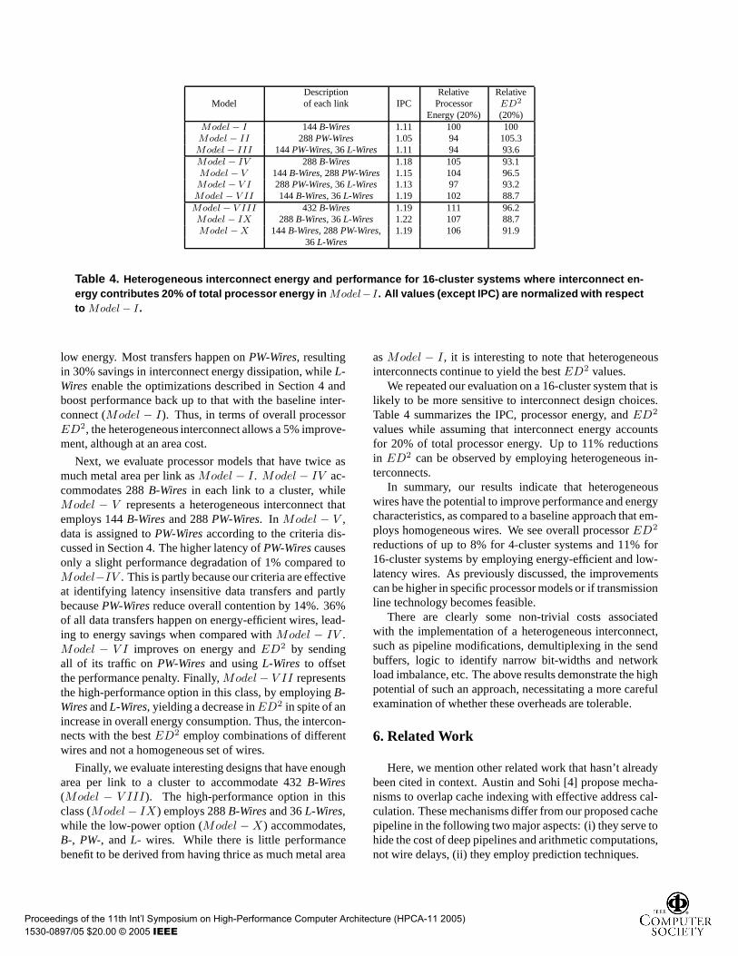
Table 4. Heterogeneous interconnect energy and performance for 16-cluster systems where interconnect en-ergy contributes 20% of total processor energy in Model−I. All values (except IPC) are normalized with respectto Model − I.
low energy. Most transfers happen on PW-Wires, resultingin 30% savings in interconnect energy dissipation, while L-Wires enable the optimizations described in Section 4 andboost performance back up to that with the baseline inter-connect (Model − I). Thus, in terms of overall processorED2, the heterogeneous interconnect allows a 5% improve-ment, although at an area cost.
Next, we evaluate processor models that have twice asmuch metal area per link as Model − I . Model − IV ac-commodates 288 B-Wires in each link to a cluster, whileModel − V represents a heterogeneous interconnect thatemploys 144 B-Wires and 288 PW-Wires. In Model − V ,data is assigned to PW-Wires according to the criteria dis-cussed in Section 4. The higher latency of PW-Wires causesonly a slight performance degradation of 1% compared toModel−IV . This is partly because our criteria are effectiveat identifying latency insensitive data transfers and partlybecause PW-Wires reduce overall contention by 14%. 36%of all data transfers happen on energy-efficient wires, lead-ing to energy savings when compared with Model − IV .Model − V I improves on energy and ED2 by sendingall of its traffic on PW-Wires and using L-Wires to offsetthe performance penalty. Finally, Model − V II representsthe high-performance option in this class, by employing B-Wires and L-Wires, yielding a decrease in ED2 in spite of anincrease in overall energy consumption. Thus, the intercon-nects with the best ED2 employ combinations of differentwires and not a homogeneous set of wires.
Finally, we evaluate interesting designs that have enougharea per link to a cluster to accommodate 432 B-Wires(Model − V III). The high-performance option in thisclass (Model − IX) employs 288 B-Wires and 36 L-Wires,while the low-power option (Model − X) accommodates,B-, PW-, and L- wires. While there is little performancebenefit to be derived from having thrice as much metal area
as Model − I , it is interesting to note that heterogeneousinterconnects continue to yield the best ED2 values.
We repeated our evaluation on a 16-cluster system that islikely to be more sensitive to interconnect design choices.Table 4 summarizes the IPC, processor energy, and ED2
values while assuming that interconnect energy accountsfor 20% of total processor energy. Up to 11% reductionsin ED2 can be observed by employing heterogeneous in-terconnects.
In summary, our results indicate that heterogeneouswires have the potential to improve performance and energycharacteristics, as compared to a baseline approach that em-ploys homogeneous wires. We see overall processor ED2
reductions of up to 8% for 4-cluster systems and 11% for16-cluster systems by employing energy-efficient and low-latency wires. As previously discussed, the improvementscan be higher in specific processor models or if transmissionline technology becomes feasible.
There are clearly some non-trivial costs associatedwith the implementation of a heterogeneous interconnect,such as pipeline modifications, demultiplexing in the sendbuffers, logic to identify narrow bit-widths and networkload imbalance, etc. The above results demonstrate the highpotential of such an approach, necessitating a more carefulexamination of whether these overheads are tolerable.
6. Related Work
Here, we mention other related work that hasn’t alreadybeen cited in context. Austin and Sohi [4] propose mecha-nisms to overlap cache indexing with effective address cal-culation. These mechanisms differ from our proposed cachepipeline in the following two major aspects: (i) they serve tohide the cost of deep pipelines and arithmetic computations,not wire delays, (ii) they employ prediction techniques.
Proceedings of the 11th Int’l Symposium on High-Performance Computer Architecture (HPCA-11 2005) 1530-0897/05 $20.00 © 2005 IEEE
A recent study by Citron [17] examines entropy withindata being transmitted on wires and identifies opportunitiesfor compression. The author suggests that if most traffic canbe compressed, the number of wires can scale down, allow-ing each wire to be fatter. Unlike our proposal, the authoremploys a single interconnect to transfer all data and not ahybrid interconnect with different latency/bandwidth/powercharacteristics. A study by Loh [31] exploits narrowbitwidths to execute multiple instructions on a single 64-bitdatapath. Performance improves because the effective issuewidth increases in some cycles. Brooks and Martonosi [13]show that in a 64-bit architecture, roughly 50% of all inte-ger ALU operations in SPEC95-Int have both operands withbit-widths less than 16 bits. In their study, this property wasexploited to reduce power consumption in integer ALUs.
The recent paper by Beckmann and Wood [12] on Trans-mission Line Caches is the only study that exploits lowlatency transmission lines at the microarchitectural level.Taylor et al. [41] define the inter-cluster communicationfabric as a Scalar Operand Network and provide a detailedanalysis of the properties of such a network and the effectof these properties on ILP extraction. Wang et al. [44] ex-amine power consumed within on-chip interconnects, witha focus on the design of router microarchitectures. No priorarchitectural work has examined trade-offs in wire charac-teristics and the design of microarchitectures to exploit avariety of wire implementations. Thus, to the best of ourknowledge, this is the first proposal of wire management atthe microarchitectural level.
7. Conclusions and Future Work
The design of the inter-cluster interconnect has a signif-icant impact on overall processor energy and performance.A single wire implementation is unable to simultaneouslymeet the high bandwidth, low-latency, and low-energy re-quirements of such an interconnect. A heterogeneous inter-connect that consists of wires with different properties canbetter meet the varying demands of inter-cluster traffic.
The paper makes three key contributions:
• We show that a low-latency low-bandwidth networkcan be effectively used to hide wire latencies and im-prove performance.
• We show that a high-bandwidth low-energy networkand an instruction assignment heuristic are effective atreducing contention cycles and total processor energy.
• We carry out a comprehensive evaluation of differ-ent combinations of heterogeneous interconnects andshow that by selecting the right combination of wires,total processor ED2 can be reduced by up to 11%,compared to a baseline processor with homogeneousinterconnects.
We therefore make a case for microarchitectural wiremanagement in future communication-bound processors.As future work, we plan to explore other applications ofheterogeneous interconnects, such as in the transfer of databetween different levels of the memory hierarchy.
References
[1] A. Aggarwal and M. Franklin. An Empirical Study of theScalability Aspects of Instruction Distribution Algorithmsfor Clustered Processors. In Proceedings of ISPASS, 2001.
[2] A. Aggarwal and M. Franklin. Hierarchical Interconnectsfor On-Chip Clustering. In Proceedings of IPDPS, April2002.
[3] S. I. Association. International Technol-ogy Roadmap for Semiconductors 2001.url:http://public.itrs.net/Files/2001ITRS/Home.htm.
[4] T. M. Austin and G. Sohi. Zero-Cycle Loads: Microarchi-tecture Support for Reducing Load Latency. In Proceedingsof MICRO-28, November 1995.
[5] H. Bakoglu. Circuits, Interconnections, and Packaging forVLSI. Addison-Wesley, 1990.
[6] R. Balasubramonian. Cluster Prefetch: Tolerating On-ChipWire Delays in Clustered Microarchitectures. In Proceed-ings of ICS-18, June 2004.
[7] R. Balasubramonian, S. Dwarkadas, and D. Albonesi. Dy-namically Managing the Communication-Parallelism Trade-Off in Future Clustered Processors. In Proceedings of ISCA-30, pages 275–286, June 2003.
[8] K. Banerjee and A. Mehrotra. A Power-optimal RepeaterInsertion Methodology for Global Interconnects in Nanome-ter Designs. IEEE Transactions on Electron Devices,49(11):2001–2007, November 2002.
[9] K. Banerjee, A. Mehrotra, A. Sangiovanni-Vincentelli, andC. Hu. On Thermal Effects in Deep Submicron VLSI Inter-connects. In Proceedings of the Design Automation Confer-ence, pages 885–891, 1999.
[10] A. Baniasadi and A. Moshovos. Instruction DistributionHeuristics for Quad-Cluster, Dynamically-Scheduled, Su-perscalar Processors. In Proceedings of MICRO-33, pages337–347, December 2000.
[11] R. Barua, W. Lee, S. Amarasinghe, and A. Agarwal. Maps:A Compiler-Managed Memory System for Raw Machines.In Proceedings of ISCA-26, May 1999.
[12] B. Beckmann and D. Wood. TLC: Transmission LineCaches. In Proceedings of MICRO-36, December 2003.
[13] D. Brooks and M. Martonosi. Dynamically Exploiting Nar-row Width Operands to Improve Processor Power and Per-formance. In Proceedings of HPCA-5, January 1999.
[14] D. Burger and T. Austin. The Simplescalar Toolset, Ver-sion 2.0. Technical Report TR-97-1342, University ofWisconsin-Madison, June 1997.
[15] R. Canal, J. M. Parcerisa, and A. Gonzalez. Dynamic Clus-ter Assignment Mechanisms. In Proceedings of HPCA-6,pages 132–142, January 2000.
[16] R. Chang, N. Talwalkar, C. Yue, and S. Wong. Near Speed-of-Light Signaling Over On-Chip Electrical Interconnects.IEEE Journal of Solid-State Circuits, 38(5):834–838, May2003.
Proceedings of the 11th Int’l Symposium on High-Performance Computer Architecture (HPCA-11 2005) 1530-0897/05 $20.00 © 2005 IEEE
[17] D. Citron. Exploiting Low Entropy to Reduce Wire Delay.IEEE Computer Architecture Letters, vol.2, January 2004.
[18] J. Collins and D. Tullsen. Clustered Multithreaded Architec-tures – Pursuing Both IPC and Cycle Time. In Proceedingsof the 18th IPDPS, April 2004.
[19] W. Dally and J. Poulton. Digital System Engineering. Cam-bridge University Press, Cambridge, UK, 1998.
[20] A. Deutsch. Electrical Characteristics of Interconnectionsfor High-Performance Systems. Proceedings of the IEEE,86(2):315–355, Feb 1998.
[21] K. Farkas, P. Chow, N. Jouppi, and Z. Vranesic. The Mul-ticluster Architecture: Reducing Cycle Time through Parti-tioning. In Proceedings of MICRO-30, pages 149–159, De-cember 1997.
[22] G. Gerosa and et al. A 2.2 W, 80 MHz SuperscalarRISC Microprocessor. IEEE Journal of Solid-State Circuits,29(12):1440–1454, December 1994.
[23] E. Gibert, J. Sanchez, and A. Gonzalez. Flexible Compiler-Managed L0 Buffers for Clustered VLIW Processors. InProceedings of MICRO-36, December 2003.
[24] R. Ho, J. Gainsley, and R. Drost. Long Wires and Asyn-chronous Control. In Proceedings of ASYNC-10, April 2004.
[25] R. Ho, K. Mai, and M. Horowitz. The Future of Wires. Pro-ceedings of the IEEE, Vol.89, No.4, April 2001.
[26] L. John. More on Finding a Single Number to Indicate Over-all Performance of a Benchmark Suite. ACM Computer Ar-chitecture News, 32(1), March 2004.
[27] U. Kapasi, W. Dally, S. Rixner, J. Owens, and B. Khailany.The Imagine Stream Processor. In Proceedings of ICCD,September 2002.
[28] S. Keckler and W. Dally. Processor Coupling: IntegratingCompile Time and Runtime Scheduling for Parallelism. InProceedings of ISCA-19, pages 202–213, May 1992.
[29] R. Kessler. The Alpha 21264 Microprocessor. IEEE Micro,19(2):24–36, March/April 1999.
[30] H.-S. Kim and J. Smith. An Instruction Set and Microar-chitecture for Instruction Level Distributed Processing. InProceedings of ISCA-29, May 2002.
[31] G. Loh. Exploiting Data-Width Locality to Increase Super-scalar Execution Bandwidth. In Proceedings of MICRO-35,November 2002.
[32] N. Magen, A. Kolodny, U. Weiser, and N. Shamir. Intercon-nect Power Dissipation in a Microprocessor. In Proceedingsof System Level Interconnect Prediction, February 2004.
[33] M. Minzuno, K. Anjo, Y. Sume, M. Fukaishi, H. Wak-abayashi, T. Mogami, T. Horiuchi, and M. Yamashina.Clock Distribution Networks with On-Chip TransmissionLines. In Proceedings of the IEEE International Intercon-nect Technology Conference, pages 3–5, 2000.
[34] M. L. Mui, K. Banerjee, and A. Mehrotra. A Global In-terconnect Optimization Scheme for Nanometer Scale VLSIWith Implications for Latency, Bandwidth, and Power Dis-sipation. IEEE Transactions on Electronic Devices, Vol.51,No.2, February 2004.
[35] R. Nagarajan, K. Sankaralingam, D. Burger, and S. Keck-ler. A Design Space Evaluation of Grid Processor Architec-tures. In Proceedings of MICRO-34, pages 40–51, Decem-ber 2001.
[36] K. Olukotun, B. Nayfeh, L. Hammond, K. Wilson, and K.-Y. Chang. The Case for a Single-Chip Multiprocessor. InProceedings of ASPLOS-VII, October 1996.
[37] J.-M. Parcerisa, J. Sahuquillo, A. Gonzalez, and J. Duato.Efficient Interconnects for Clustered Microarchitectures. InProceedings of PACT, September 2002.
[38] P. Racunas and Y. Patt. Partitioned First-Level Cache Designfor Clustered Microarchitectures. In Proceedings of ICS-17,June 2003.
[39] J. Sanchez and A. Gonzalez. Modulo Scheduling for a Fully-Distributed Clustered VLIW Architecture. In Proceedings ofMICRO-33, pages 124–133, December 2000.
[40] T. Sherwood, E. Perelman, G. Hamerly, and B. Calder. Au-tomatically Characterizing Large Scale Program Behavior.In Proceedings of ASPLOS-X, October 2002.
[41] M. Taylor, W. Lee, S. Amarasinghe, and A. Agarwal. ScalarOperand Networks: On-Chip Interconnect for ILP in Parti-tioned Architectures. In Proceedings of HPCA-9, February2003.
[42] M. Taylor, W. Lee, J. Miller, D. Wentzlaff, I. Bratt, B. Green-wald, H. Hoffmann, P. Johnson, J. Kim, J. Psota, A. Raraf,N. Shnidman, V. Strumpen, M. Frank, S. Amarasinghe, andA. Agarwal. Evaluation of the Raw Microprocessor: AnExposed-Wire-Delay Architecture for ILP and Streams. InProceedings of ISCA-31, June 2004.
[43] E. Tune, D. Liang, D. Tullsen, and B. Calder. DynamicPrediction of Critical Path Instructions. In Proceedings ofHPCA-7, pages 185–196, January 2001.
[44] H.-S. Wang, L.-S. Peh, and S. Malik. Power-Driven Designof Router Microarchitectures in On-Chip Networks. In Pro-ceedings of MICRO-36, December 2003.
[45] J. Warnock, J. Keaty, J. Petrovick, J. Clabes, C. Kircher,B. Krauter, P. Restle, B. Zoric, and C. Anderson. The Cir-cuit and Physical Design of the POWER4 Microprocessor.IBM Journal of Research and Development, 46(1):27–51,Jan 2002.
[46] T. Xanthopoulos, D. Bailey, A. Gangwar, M. Gowan,A. Jain, and B. Prewitt. The Design and Analysis of theClock Distribution Network for a 1.2GHz Alpha Micropro-cessor. In Proceedings of the IEEE International Solid-StateCircuits Conference, pages 402–403, 2001.
[47] J. Yang, Y. Zhang, and R. Gupta. Frequent Value Compres-sion in Data Caches. In Proceedings of MICRO-33, pages258–265, December 2000.
Proceedings of the 11th Int’l Symposium on High-Performance Computer Architecture (HPCA-11 2005) 1530-0897/05 $20.00 © 2005 IEEE
Related Documents