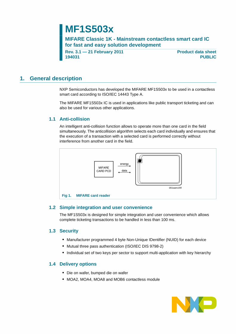
1. General description NXP Semiconductors has developed the MIFARE MF1S503x to be used in a contactless smart card according to ISO/IEC 14443 Type A. The MIFARE MF1S503x IC is used in applications like public transport ticketing and can also be used for various other applications. 1.1 Anti-collision An intelligent anti-collision function allows to operate more than one card in the field simultaneously. The anticollision algorithm selects each card individually and ensures that the execution of a transaction with a selected card is performed correctly without interference from another card in the field. 1.2 Simple integration and user convenience The MF1S503x is designed for simple integration and user convenience which allows complete ticketing transactions to be handled in less than 100 ms. 1.3 Security • Manufacturer programmed 4 byte Non-Unique IDentifier (NUID) for each device • Mutual three pass authentication (ISO/IEC DIS 9798-2) • Individual set of two keys per sector to support multi-application with key hierarchy 1.4 Delivery options • Die on wafer, bumped die on wafer • MOA2, MOA4, MOA8 and MOB6 contactless module MF1S503x MIFARE Classic 1K - Mainstream contactless smart card IC for fast and easy solution development Rev. 3.1 — 21 February 2011 194031 Product data sheet PUBLIC Fig 1. MIFARE card reader 001aam199 MIFARE CARD PCD energy data

Welcome message from author
This document is posted to help you gain knowledge. Please leave a comment to let me know what you think about it! Share it to your friends and learn new things together.
Transcript
1. General description
NXP Semiconductors has developed the MIFARE MF1S503x to be used in a contactless smart card according to ISO/IEC 14443 Type A.
The MIFARE MF1S503x IC is used in applications like public transport ticketing and can also be used for various other applications.
1.1 Anti-collisionAn intelligent anti-collision function allows to operate more than one card in the field simultaneously. The anticollision algorithm selects each card individually and ensures that the execution of a transaction with a selected card is performed correctly without interference from another card in the field.
1.2 Simple integration and user convenienceThe MF1S503x is designed for simple integration and user convenience which allows complete ticketing transactions to be handled in less than 100 ms.
1.3 Security
• Manufacturer programmed 4 byte Non-Unique IDentifier (NUID) for each device • Mutual three pass authentication (ISO/IEC DIS 9798-2)• Individual set of two keys per sector to support multi-application with key hierarchy
1.4 Delivery options
• Die on wafer, bumped die on wafer• MOA2, MOA4, MOA8 and MOB6 contactless module
MF1S503xMIFARE Classic 1K - Mainstream contactless smart card IC for fast and easy solution developmentRev. 3.1 — 21 February 2011194031
Product data sheetPUBLIC
Fig 1. MIFARE card reader
001aam199
MIFARECARD PCD
energy
data
MF1S503x All information provided in this document is subject to legal disclaimers. © NXP B.V. 2011. All rights reserved.
Product data sheetPUBLIC
Rev. 3.1 — 21 February 2011194031 2 of 37
NXP Semiconductors MF1S503xMIFARE Classic 1K - Mainstream contactless smart card IC
2. Features and benefits
2.1 EEPROM
3. Applications
4. Quick reference data
[1] LCR meter, Tamb = 22 °C, fi = 13.56 MHz, 2 V RMS.
Contactless transmission of data and supply energy
Operating distance up to 100 mm depending on antenna geometry and reader configuration
Operating frequency of 13.56 MHz Data transfer of 106 kbit/sData integrity of 16-bit CRC, parity, bit coding, bit counting
Anti-collision
Typical ticketing transaction time of less than 100 ms (including backup management)
1 kB, organized in 16 sectors of 4 blocks (one block consists of 16 byte)
User definable access conditions for each memory block
Data retention time of 10 years Write endurance 100.000 cycles
Public transportation Access management Electronic toll collection Car parkingSchool and campus cards Employee cardsInternet cafés Loyalty
Table 1. Quick reference dataSymbol Parameter Conditions Min Typ Max UnitCi input capacitance [1] 14.4 16.1 17.4 pF
fi input frequency - 13.56 - MHz
EEPROM characteristicstret retention time Tamb = 22 °C 10 - - year
Nendu(W) write endurance Tamb = 22 °C 100000 200000 - cycle
MF1S503x All information provided in this document is subject to legal disclaimers. © NXP B.V. 2011. All rights reserved.
Product data sheetPUBLIC
Rev. 3.1 — 21 February 2011194031 3 of 37
NXP Semiconductors MF1S503xMIFARE Classic 1K - Mainstream contactless smart card IC
5. Ordering information
6. Block diagram
Table 2. Ordering informationType number Package
Commercial Name
Name Description Version
MF1S5035DUD/L FFC Bump - 8 inch wafer, 120 μm thickness, laser diced, on film frame carrier, electronic fail die marking according to SECSII format), Au bumps
not applicable
MF1S5035DUH/L FFC - 8 inch wafer, 120 μm thickness, laser diced, on film frame carrier, electronic fail die marking according to SECSII format)
not applicable
MF1S5037DUG FFC Bump - 8 inch wafer, 150 μm thickness, on film frame carrier, electronic fail die marking according to SECSII format), Au bumps
not applicable
MF1S5037DUA FFC - 8 inch wafer, 150 μm thickness, on film frame carrier, electronic fail die marking according to SECSII format)
not applicable
MF1S5030DA3 MOA2 PLLMC plastic leadless module carrier package; 35 mm wide tape SOT500-1
MF1S5030DA4 MOA4 PLLMC plastic leadless module carrier package; 35 mm wide tape SOT500-2
MF1S5030DA6 MOB6 PLLMC plastic leadless module carrier package; 35 mm wide tape SOT500-3
MF1S5030DA8 MOA8 PLLMC plastic leadless module carrier package; 35 mm wide tape SOT500-4
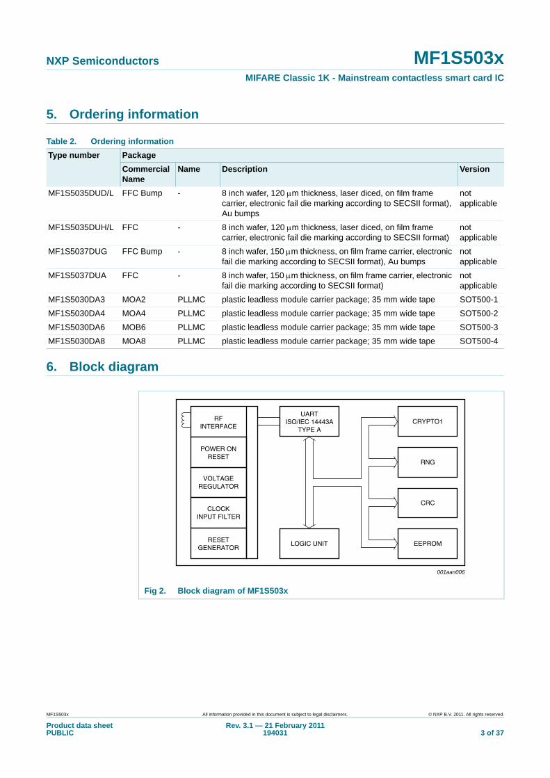
Fig 2. Block diagram of MF1S503x
001aan006
RFINTERFACE
UARTISO/IEC 14443A
TYPE A
LOGIC UNIT
RNG
CRC
EEPROM
CRYPTO1
POWER ONRESET
VOLTAGEREGULATOR
CLOCKINPUT FILTER
RESETGENERATOR
MF1S503x All information provided in this document is subject to legal disclaimers. © NXP B.V. 2011. All rights reserved.
Product data sheetPUBLIC
Rev. 3.1 — 21 February 2011194031 4 of 37
NXP Semiconductors MF1S503xMIFARE Classic 1K - Mainstream contactless smart card IC
7. Pinning information
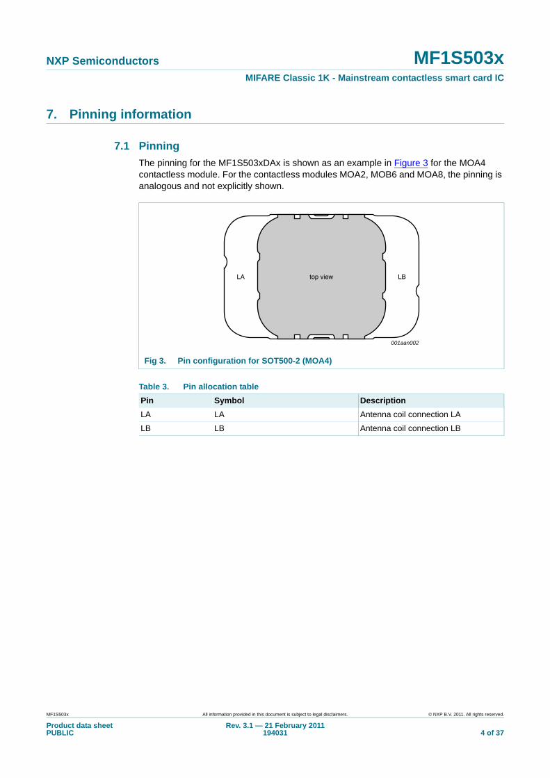
7.1 PinningThe pinning for the MF1S503xDAx is shown as an example in Figure 3 for the MOA4 contactless module. For the contactless modules MOA2, MOB6 and MOA8, the pinning is analogous and not explicitly shown.
Fig 3. Pin configuration for SOT500-2 (MOA4)
Table 3. Pin allocation tablePin Symbol DescriptionLA LA Antenna coil connection LA
LB LB Antenna coil connection LB
001aan002
LA LBtop view
MF1S503x All information provided in this document is subject to legal disclaimers. © NXP B.V. 2011. All rights reserved.
Product data sheetPUBLIC
Rev. 3.1 — 21 February 2011194031 5 of 37
NXP Semiconductors MF1S503xMIFARE Classic 1K - Mainstream contactless smart card IC
8. Functional description
8.1 Block descriptionThe MF1S503x chip consists of a 1 kB EEPROM, RF interface and Digital Control Unit. Energy and data are transferred via an antenna consisting of a coil with a small number of turns which is directly connected to the MF1S503x. No further external components are necessary. Refer to the document Ref. 1 for details on antenna design.
• RF interface:– Modulator/demodulator– Rectifier– Clock regenerator– Power-On Reset (POR)– Voltage regulator
• Anti-collision: Multiple cards in the field may be selected and managed in sequence• Authentication: Preceding any memory operation the authentication procedure
ensures that access to a block is only possible via the two keys specified for each block
• Control and Arithmetic Logic Unit: Values are stored in a special redundant format and can be incremented and decremented
• EEPROM interface• Crypto unit: The CRYPTO1 stream cipher of the MF1S503x is used for authentication
and encryption of data exchange.• EEPROM: 1 kB is organized in 16 sectors with 4 blocks each. A block contains
16 bytes. The last block of each sector is called “trailer”, which contains two secret keys and programmable access conditions for each block in this sector.
8.2 Communication principleThe commands are initiated by the reader and controlled by the Digital Control Unit of the MF1S503x. The command response is depending on the state of the IC and for memory operations also on the access conditions valid for the corresponding sector.
8.2.1 Request standard/allAfter Power-On Reset (POR) the card answers to a request REQA or wakeup WUPA command with the answer to request code (see Section 9.4, ATQA according to ISO/IEC 14443A).
8.2.2 Anti-collision loopIn the anti-collision loop the identifier of a card is read. If there are several cards in the operating field of the reader, they can be distinguished by their identifier and one can be selected (select card) for further transactions. The unselected cards return to the idle state and wait for a new request command.
Remark: The identifier retrieved from the card is not defined to be unique. For further information regarding handling of non-unique identifiers see Ref. 11.
MF1S503x All information provided in this document is subject to legal disclaimers. © NXP B.V. 2011. All rights reserved.
Product data sheetPUBLIC
Rev. 3.1 — 21 February 2011194031 6 of 37
NXP Semiconductors MF1S503xMIFARE Classic 1K - Mainstream contactless smart card IC
8.2.3 Select cardWith the select card command the reader selects one individual card for authentication and memory related operations. The card returns the Select Acknowledge (SAK) code which determines the type of the selected card, see Section 9.4. For further details refer to the document Ref. 7.
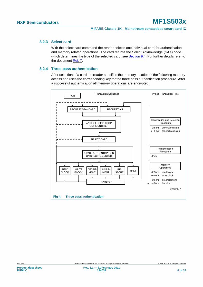
8.2.4 Three pass authenticationAfter selection of a card the reader specifies the memory location of the following memory access and uses the corresponding key for the three pass authentication procedure. After a successful authentication all memory operations are encrypted.
Fig 4. Three pass authentication
001aan017
REQUEST STANDARD
Transaction Sequence Typical Transaction Time
SELECT CARD
POR
TRANSFER
ANTICOLLISION LOOPGET IDENTIFIER
3 PASS AUTHENTICATIONON SPECIFIC SECTOR
READBLOCK
WRITEBLOCK
DECRE-MENT
INCRE-MENT
RE-STORE
HALT
REQUEST ALL
Identification and SelectionProcedure
without collision~2.5 ms
AuthenticationProcedure
~2 ms
for each collision+~1 ms
MemoryOperations
read block~2.5 mswrite block~6.0 ms
de-/increment~2.5 mstransfer~4.5 ms
MF1S503x All information provided in this document is subject to legal disclaimers. © NXP B.V. 2011. All rights reserved.
Product data sheetPUBLIC
Rev. 3.1 — 21 February 2011194031 7 of 37
NXP Semiconductors MF1S503xMIFARE Classic 1K - Mainstream contactless smart card IC
8.2.5 Memory operationsAfter authentication any of the following operations may be performed:
• Read block• Write block• Decrement: Decrements the contents of a block and stores the result in an internal
data-register• Increment: Increments the contents of a block and stores the result in an internal
data-register• Restore: Moves the contents of a block into an internal data-register• Transfer: Writes the contents of the temporary internal data-register to a value block
8.3 Data integrityFollowing mechanisms are implemented in the contactless communication link between reader and card to ensure very reliable data transmission:
• 16 bits CRC per block• Parity bits for each byte• Bit count checking• Bit coding to distinguish between “1”, “0” and “no information”• Channel monitoring (protocol sequence and bit stream analysis)
8.4 Three pass authentication sequence
1. The reader specifies the sector to be accessed and chooses key A or B.2. The card reads the secret key and the access conditions from the sector trailer. Then
the card sends a random number as the challenge to the reader (pass one).3. The reader calculates the response using the secret key and additional input. The
response, together with a random challenge from the reader, is then transmitted to the card (pass two).
4. The card verifies the response of the reader by comparing it with its own challenge and then it calculates the response to the challenge and transmits it (pass three).
5. The reader verifies the response of the card by comparing it to its own challenge.
After transmission of the first random challenge the communication between card and reader is encrypted.
MF1S503x All information provided in this document is subject to legal disclaimers. © NXP B.V. 2011. All rights reserved.
Product data sheetPUBLIC
Rev. 3.1 — 21 February 2011194031 8 of 37
NXP Semiconductors MF1S503xMIFARE Classic 1K - Mainstream contactless smart card IC
8.5 RF interfaceThe RF-interface is according to the standard for contactless smart cards ISO/IEC 14443 A.
For operation, the carrier field from the reader always needs to be present (with short pauses when transmitting), as it is used for the power supply of the card.
For both directions of data communication there is only one start bit at the beginning of each frame. Each byte is transmitted with a parity bit (odd parity) at the end. The LSB of the byte with the lowest address of the selected block is transmitted first. The maximum frame length is 163 bits (16 data bytes + 2 CRC bytes = 16 × 9 + 2 × 9 + 1 start bit).
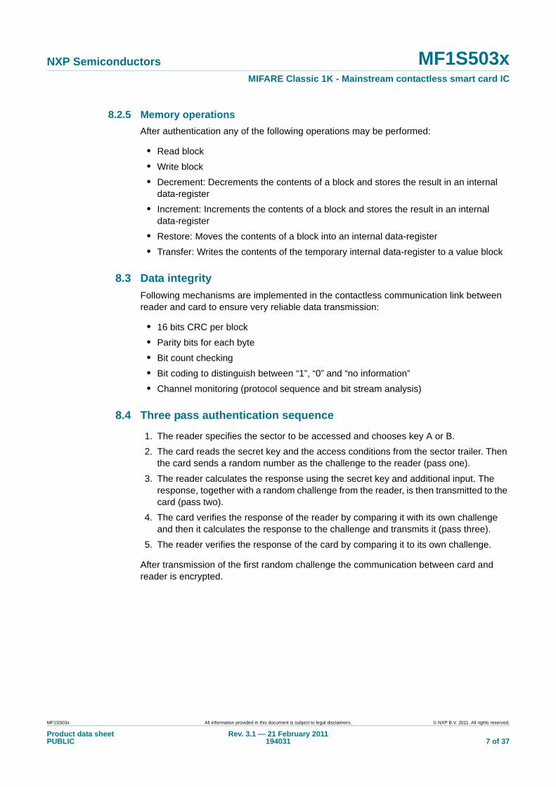
8.6 Memory organizationThe 1024 × 8 bit EEPROM memory is organized in 16 sectors of 4 blocks. One block contains 16 bytes.
Fig 5. Memory organization
001aan011
Byte Number within a Block
15141312111098765
Key A Access Bits Key B
43210Block
3
Sector
15
2
1
0
Description
Sector Trailer 15
Data
Data
Data
Sector Trailer 14
Data
Data
Data
Sector Trailer 0
Data
Data
Manufacturer Block
Sector Trailer 1
Data
Data
Data
314
2
1
0
31
2
1
0
30
2
1
0
:
:
:
:
:
:
Key A Access Bits Key B
Key A Access Bits Key B
Key A Access Bits
Manufacturer Data
Key B
MF1S503x All information provided in this document is subject to legal disclaimers. © NXP B.V. 2011. All rights reserved.
Product data sheetPUBLIC
Rev. 3.1 — 21 February 2011194031 9 of 37
NXP Semiconductors MF1S503xMIFARE Classic 1K - Mainstream contactless smart card IC
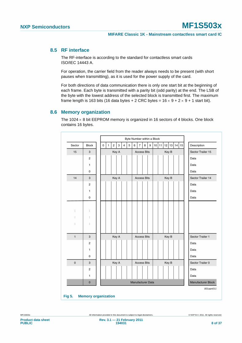
8.6.1 Manufacturer blockThis is the first data block (block 0) of the first sector (sector 0). It contains the IC manufacturer data. This block is programmed and write protected in the production test.
8.6.2 Data blocksAll sectors contain 3 blocks of 16 bytes for storing data (Sector 0 contains only two data blocks and the read-only manufacturer block).
The data blocks can be configured by the access bits as
• read/write blocks• value blocks
Value blocks can be used for e.g. electronic purse applications, where additional commands like increment and decrement for direct control of the stored value are provided.
A successful authentication has to be performed to allow any memory operation.
Remark: The default content of the data blocks at delivery is not defined.
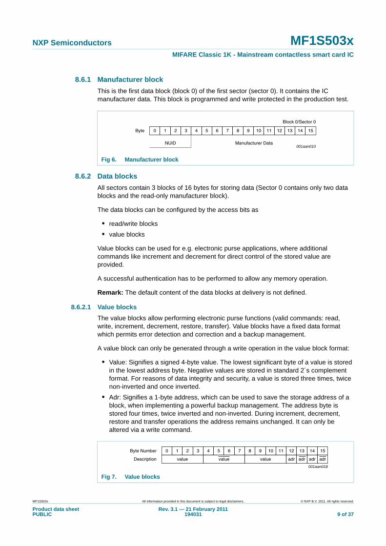
8.6.2.1 Value blocksThe value blocks allow performing electronic purse functions (valid commands: read, write, increment, decrement, restore, transfer). Value blocks have a fixed data format which permits error detection and correction and a backup management.
A value block can only be generated through a write operation in the value block format:
• Value: Signifies a signed 4-byte value. The lowest significant byte of a value is stored in the lowest address byte. Negative values are stored in standard 2´s complement format. For reasons of data integrity and security, a value is stored three times, twice non-inverted and once inverted.
• Adr: Signifies a 1-byte address, which can be used to save the storage address of a block, when implementing a powerful backup management. The address byte is stored four times, twice inverted and non-inverted. During increment, decrement, restore and transfer operations the address remains unchanged. It can only be altered via a write command.
Fig 6. Manufacturer block
001aan010
1514131211109876543
NUID Manufacturer Data
Block 0/Sector 0
21Byte 0
Fig 7. Value blocks
001aan018
151413121110987654321Byte Number 0
adradradradrvalue valuevalueDescription
MF1S503x All information provided in this document is subject to legal disclaimers. © NXP B.V. 2011. All rights reserved.
Product data sheetPUBLIC
Rev. 3.1 — 21 February 2011194031 10 of 37
NXP Semiconductors MF1S503xMIFARE Classic 1K - Mainstream contactless smart card IC
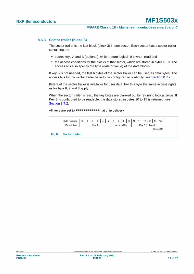
8.6.3 Sector trailer (block 3)The sector trailer is the last block (block 3) in one sector. Each sector has a sector trailer containing the
• secret keys A and B (optional), which return logical “0”s when read and • the access conditions for the blocks of that sector, which are stored in bytes 6...9. The
access bits also specify the type (data or value) of the data blocks.
If key B is not needed, the last 6 bytes of the sector trailer can be used as data bytes. The access bits for the sector trailer have to be configured accordingly, see Section 8.7.2.
Byte 9 of the sector trailer is available for user data. For this byte the same access rights as for byte 6, 7 and 8 apply.
When the sector trailer is read, the key bytes are blanked out by returning logical zeros. If Key B is configured to be readable, the data stored in bytes 10 to 15 is returned, see Section 8.7.2.
All keys are set to FFFFFFFFFFFFh at chip delivery.
Fig 8. Sector trailer
001aan013
151413121110987654321Byte Number 0
Key A Key B (optional)Access BitsDescription
MF1S503x All information provided in this document is subject to legal disclaimers. © NXP B.V. 2011. All rights reserved.
Product data sheetPUBLIC
Rev. 3.1 — 21 February 2011194031 11 of 37
NXP Semiconductors MF1S503xMIFARE Classic 1K - Mainstream contactless smart card IC
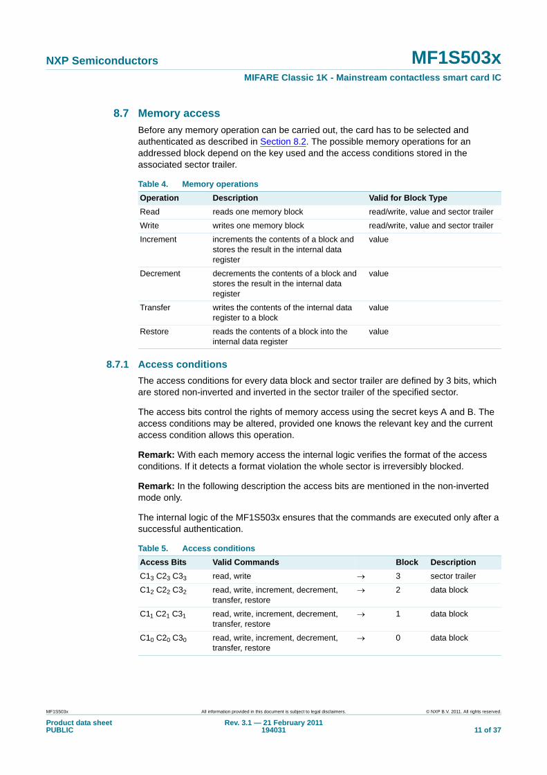
8.7 Memory accessBefore any memory operation can be carried out, the card has to be selected and authenticated as described in Section 8.2. The possible memory operations for an addressed block depend on the key used and the access conditions stored in the associated sector trailer.
8.7.1 Access conditionsThe access conditions for every data block and sector trailer are defined by 3 bits, which are stored non-inverted and inverted in the sector trailer of the specified sector.
The access bits control the rights of memory access using the secret keys A and B. The access conditions may be altered, provided one knows the relevant key and the current access condition allows this operation.
Remark: With each memory access the internal logic verifies the format of the access conditions. If it detects a format violation the whole sector is irreversibly blocked.
Remark: In the following description the access bits are mentioned in the non-inverted mode only.
The internal logic of the MF1S503x ensures that the commands are executed only after a successful authentication.
Table 4. Memory operationsOperation Description Valid for Block TypeRead reads one memory block read/write, value and sector trailer
Write writes one memory block read/write, value and sector trailer
Increment increments the contents of a block and stores the result in the internal data register
value
Decrement decrements the contents of a block and stores the result in the internal data register
value
Transfer writes the contents of the internal data register to a block
value
Restore reads the contents of a block into the internal data register
value
Table 5. Access conditionsAccess Bits Valid Commands Block DescriptionC13 C23 C33 read, write → 3 sector trailer
C12 C22 C32 read, write, increment, decrement, transfer, restore
→ 2 data block
C11 C21 C31 read, write, increment, decrement, transfer, restore
→ 1 data block
C10 C20 C30 read, write, increment, decrement, transfer, restore
→ 0 data block
MF1S503x All information provided in this document is subject to legal disclaimers. © NXP B.V. 2011. All rights reserved.
Product data sheetPUBLIC
Rev. 3.1 — 21 February 2011194031 12 of 37
NXP Semiconductors MF1S503xMIFARE Classic 1K - Mainstream contactless smart card IC
8.7.2 Access conditions for the sector trailerDepending on the access bits for the sector trailer (block 3) the read/write access to the keys and the access bits is specified as ‘never’, ‘key A’, ‘key B’ or key A|B’ (key A or key B).
On chip delivery the access conditions for the sector trailers and key A are predefined as transport configuration. Since key B may be read in the transport configuration, new cards must be authenticated with key A. Since the access bits themselves can also be blocked, special care has to be taken during personalization of cards.
[1] for this access condition key B is readable and may be used for data
Fig 9. Access conditions
001aan003
151413121110987654321Byte Number
Description
0
Key A Key B (optional)Access Bits
user data
Byte 6 C23 C22 C21 C20 C13 C12 C11 C10
7Bit 6 5 4 3 2 1 0
Byte 7 C13 C12 C11 C10 C33 C32 C31 C30
Byte 8 C33 C32 C31 C30 C23 C22 C21 C20
Byte 9
Table 6. Access conditions for the sector trailerAccess bits Access condition for Remark
KEYA Access bits KEYBC1 C2 C3 read write read write read write
0 0 0 never key A key A never key A key A Key B may be read[1]
0 1 0 never never key A never key A never Key B may be read[1]
1 0 0 never key B key A|B never never key B
1 1 0 never never key A|B never never never
0 0 1 never key A key A key A key A key A Key B may be read,transport configuration[1]
0 1 1 never key B key A|B key B never key B
1 0 1 never never key A|B key B never never
1 1 1 never never key A|B never never never
MF1S503x All information provided in this document is subject to legal disclaimers. © NXP B.V. 2011. All rights reserved.
Product data sheetPUBLIC
Rev. 3.1 — 21 February 2011194031 13 of 37
NXP Semiconductors MF1S503xMIFARE Classic 1K - Mainstream contactless smart card IC
8.7.3 Access conditions for data blocksDepending on the access bits for data blocks (blocks 0...2) the read/write access is specified as ‘never’, ‘key A’, ‘key B’ or ‘key A|B’ (key A or key B). The setting of the relevant access bits defines the application and the corresponding applicable commands.
• Read/write block: the operations read and write are allowed.• Value block: Allows the additional value operations increment, decrement, transfer
and restore. With access condition ‘001’ only read and decrement are possible which reflects a non-rechargeable card. For access condition ‘110’ recharging is possible by using key B.
• Manufacturer block: the read-only condition is not affected by the access bits setting!• Key management: in transport configuration key A must be used for authentication
[1] if Key B may be read in the corresponding Sector Trailer it cannot serve for authentication (all grey marked lines in previous table). As a consequences, if the reader authenticates any block of a sector which uses the grey marked access conditions and using key B, the card will refuse any subsequent memory access after authentication.
Table 7. Access conditions for data blocksAccess bits Access condition for ApplicationC1 C2 C3 read write increment decrement,
transfer, restore
0 0 0 key A|B[1] key A|B1 key A|B1 key A|B1 transport configuration
0 1 0 key A|B[1] never never never read/write block
1 0 0 key A|B[1] key B1 never never read/write block
1 1 0 key A|B[1] key B1 key B1 key A|B1 value block
0 0 1 key A|B[1] never never key A|B1 value block
0 1 1 key B[1] key B1 never never read/write block
1 0 1 key B[1] never never never read/write block
1 1 1 never never never never read/write block
MF1S503x All information provided in this document is subject to legal disclaimers. © NXP B.V. 2011. All rights reserved.
Product data sheetPUBLIC
Rev. 3.1 — 21 February 2011194031 14 of 37
NXP Semiconductors MF1S503xMIFARE Classic 1K - Mainstream contactless smart card IC
9. Command overview
The MIFARE Classic card activation follows the ISO/IEC 14443-3 type A. After the MIFARE Classic card has been selected, it can either be deactivated using the ISO/IEC 14443 Halt command, or the MIFARE Classic commands can be performed. For more details about the card activation refer to Ref. 9.
9.1 MIFARE Classic command overviewAll MIFARE Classic commands use the MIFARE Crypto1 and require an authentication.
All available commands for the MIFARE Classic are shown in Table 8.
All the commands use the coding and framing as described in Ref. 8 and Ref. 9 if not otherwise specified.
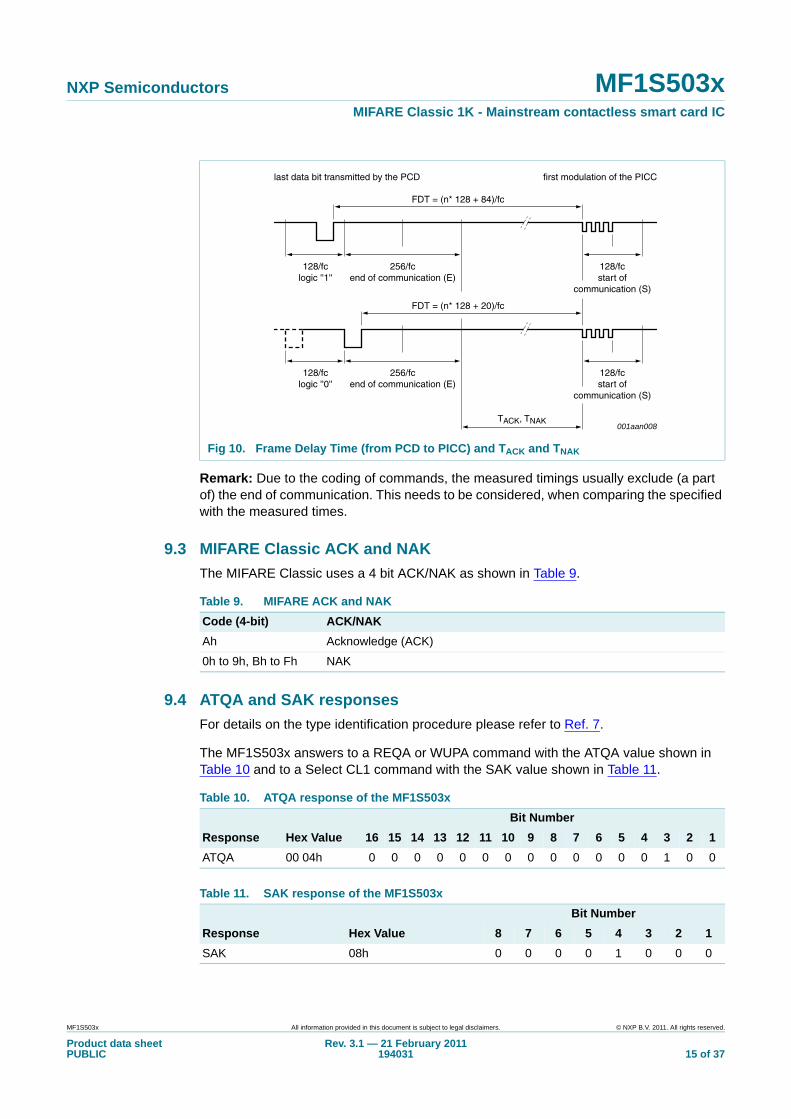
9.2 TimingsThe timing shown in this document are not to scale and values are rounded to 1 μs.
All the given times refer to the data frames including start of communication and end of communication, but do not include the encoding (like the Miller pulses).
Consequently a data frame sent by the PCD contains the start of communication (1 “start bit”) and the end of communication (one logic 0 + 1 bit length of unmodulated carrier).
A data frame sent by the PICC contains the start of communication (1 “start bit”) and the end of communication (1 bit length of no subcarrier).
All timing can be measured according to ISO/IEC 14443-3 frame specification as shown for the Frame Delay Time in Figure 10. For more details refer to Ref. 8 and Ref. 9.
The frame delay time from PICC to PCD must be at least 87 μs.
Table 8. Command overviewCommand ISO/IEC 14443 Command code
(hexadecimal)Request REQA 26h (7 bit)
Wake-up WUPA 52h (7 bit)
Anti-collision CL1 Anti-collision CL1 93h 20h
Select CL1 Select CL1 93h 70h
Halt Halt 50h 00h
Authentication with Key A - 60h
Authentication with Key B - 61h
MIFARE Read - 30h
MIFARE Write - A0h
MIFARE Decrement - C0h
MIFARE Increment - C1h
MIFARE Restore - C2h
MIFARE Transfer - B0h
MF1S503x All information provided in this document is subject to legal disclaimers. © NXP B.V. 2011. All rights reserved.
Product data sheetPUBLIC
Rev. 3.1 — 21 February 2011194031 15 of 37
NXP Semiconductors MF1S503xMIFARE Classic 1K - Mainstream contactless smart card IC
Remark: Due to the coding of commands, the measured timings usually exclude (a part of) the end of communication. This needs to be considered, when comparing the specified with the measured times.
9.3 MIFARE Classic ACK and NAK The MIFARE Classic uses a 4 bit ACK/NAK as shown in Table 9.
9.4 ATQA and SAK responsesFor details on the type identification procedure please refer to Ref. 7.
The MF1S503x answers to a REQA or WUPA command with the ATQA value shown in Table 10 and to a Select CL1 command with the SAK value shown in Table 11.
Fig 10. Frame Delay Time (from PCD to PICC) and TACK and TNAK
001aan008
last data bit transmitted by the PCD
FDT = (n* 128 + 84)/fc
256/fcend of communication (E)
128/fclogic ''1''
128/fcstart of
communication (S)
first modulation of the PICC
FDT = (n* 128 + 20)/fc
256/fcend of communication (E)
TACK, TNAK
128/fclogic ''0''
128/fcstart of
communication (S)
Table 9. MIFARE ACK and NAKCode (4-bit) ACK/NAKAh Acknowledge (ACK)
0h to 9h, Bh to Fh NAK
Table 10. ATQA response of the MF1S503xBit Number
Response Hex Value 16 15 14 13 12 11 10 9 8 7 6 5 4 3 2 1ATQA 00 04h 0 0 0 0 0 0 0 0 0 0 0 0 0 1 0 0
Table 11. SAK response of the MF1S503xBit Number
Response Hex Value 8 7 6 5 4 3 2 1SAK 08h 0 0 0 0 1 0 0 0
MF1S503x All information provided in this document is subject to legal disclaimers. © NXP B.V. 2011. All rights reserved.
Product data sheetPUBLIC
Rev. 3.1 — 21 February 2011194031 16 of 37
NXP Semiconductors MF1S503xMIFARE Classic 1K - Mainstream contactless smart card IC
10. MIFARE Classic commands
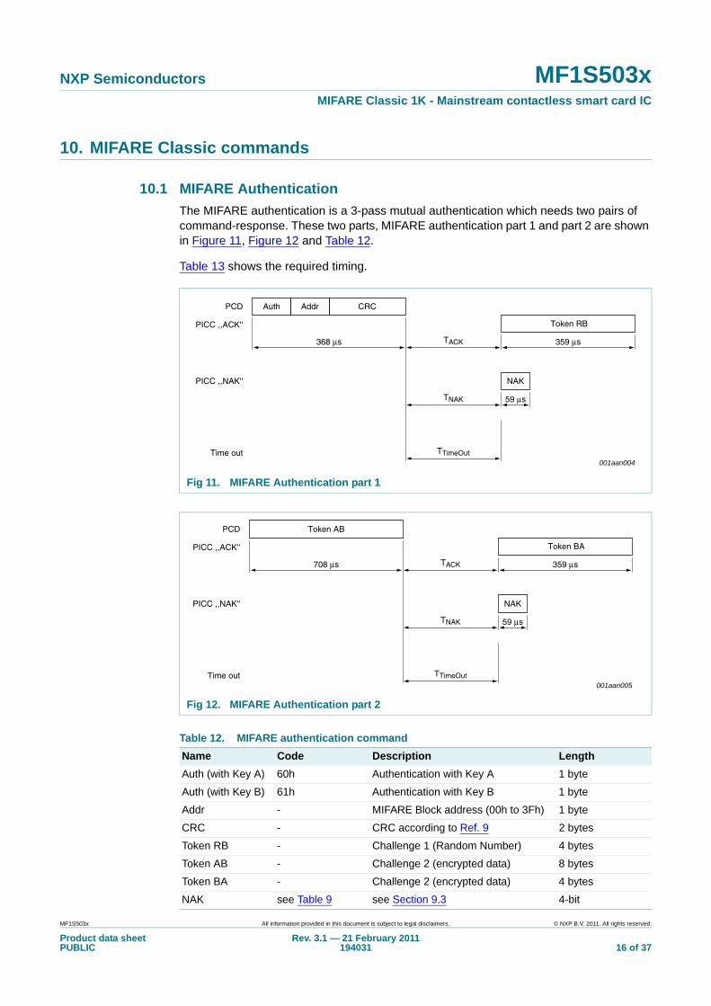
10.1 MIFARE AuthenticationThe MIFARE authentication is a 3-pass mutual authentication which needs two pairs of command-response. These two parts, MIFARE authentication part 1 and part 2 are shown in Figure 11, Figure 12 and Table 12.
Table 13 shows the required timing.
Fig 11. MIFARE Authentication part 1
Fig 12. MIFARE Authentication part 2
Table 12. MIFARE authentication commandName Code Description LengthAuth (with Key A) 60h Authentication with Key A 1 byte
Auth (with Key B) 61h Authentication with Key B 1 byte
Addr - MIFARE Block address (00h to 3Fh) 1 byte
CRC - CRC according to Ref. 9 2 bytes
Token RB - Challenge 1 (Random Number) 4 bytes
Token AB - Challenge 2 (encrypted data) 8 bytes
Token BA - Challenge 2 (encrypted data) 4 bytes
NAK see Table 9 see Section 9.3 4-bit
001aan004
CRCAddrPCD Auth
Token RBPICC ,,ACK''
368 μs 359 μs
PICC ,,NAK'' NAK
Time out TTimeOut
TNAK
TACK
59 μs
001aan005
Token ABPCD
Token BAPICC ,,ACK''
708 μs 359 μs
PICC ,,NAK'' NAK
Time out TTimeOut
TNAK
TACK
59 μs
MF1S503x All information provided in this document is subject to legal disclaimers. © NXP B.V. 2011. All rights reserved.
Product data sheetPUBLIC
Rev. 3.1 — 21 February 2011194031 17 of 37
NXP Semiconductors MF1S503xMIFARE Classic 1K - Mainstream contactless smart card IC
Remark: The minimum required time between MIFARE Authentication part 1 and part 2 is the minimum required FDT according to Ref. 9. There is no maximum time specified.
Remark: The MIFARE authentication and encryption requires an MIFARE reader IC (e.g. the CL RC632). For more details about the authentication command refer to the corresponding data sheet (e.g. Ref. 10).
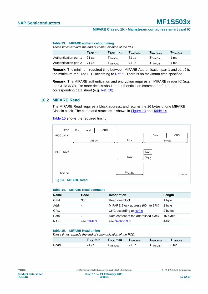
10.2 MIFARE ReadThe MIFARE Read requires a block address, and returns the 16 bytes of one MIFARE Classic block. The command structure is shown in Figure 13 and Table 14.
Table 15 shows the required timing.
Table 13. MIFARE authentication timingThese times exclude the end of communication of the PCD.
TACK min TACK max TNAK min TNAK max TTimeOut
Authentication part 1 71 μs TTimeOut 71 μs TTimeOut 1 ms
Authentication part 2 71 μs TTimeOut 71 μs TTimeOut 1 ms
Fig 13. MIFARE Read
Table 14. MIFARE Read commandName Code Description LengthCmd 30h Read one block 1 byte
Addr - MIFARE Block address (00h to 3Fh) 1 byte
CRC - CRC according to Ref. 9 2 bytes
Data - Data content of the addressed block 16 bytes
NAK see Table 9 see Section 9.3 4-bit
Table 15. MIFARE Read timingThese times exclude the end of communication of the PCD.
TACK min TACK max TNAK min TNAK max TTimeOut
Read 71 μs TTimeOut 71 μs TTimeOut 5 ms
001aan014
CRC
CRC
AddrPCD Cmd
DataPICC ,,ACK''
368 μs 1548 μs
PICC ,,NAK'' NAK
Time out TTimeOut
TNAK
TACK
59 μs
MF1S503x All information provided in this document is subject to legal disclaimers. © NXP B.V. 2011. All rights reserved.
Product data sheetPUBLIC
Rev. 3.1 — 21 February 2011194031 18 of 37
NXP Semiconductors MF1S503xMIFARE Classic 1K - Mainstream contactless smart card IC
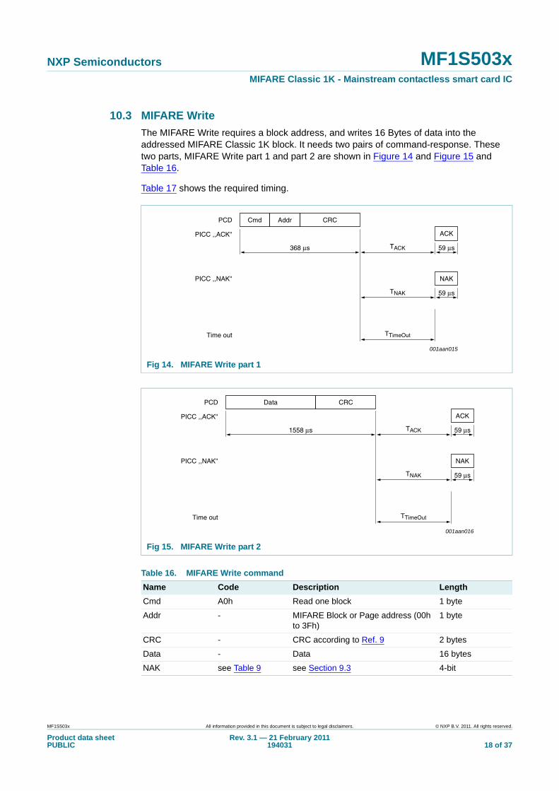
10.3 MIFARE WriteThe MIFARE Write requires a block address, and writes 16 Bytes of data into the addressed MIFARE Classic 1K block. It needs two pairs of command-response. These two parts, MIFARE Write part 1 and part 2 are shown in Figure 14 and Figure 15 and Table 16.
Table 17 shows the required timing.
Fig 14. MIFARE Write part 1
Fig 15. MIFARE Write part 2
Table 16. MIFARE Write commandName Code Description LengthCmd A0h Read one block 1 byte
Addr - MIFARE Block or Page address (00h to 3Fh)
1 byte
CRC - CRC according to Ref. 9 2 bytes
Data - Data 16 bytes
NAK see Table 9 see Section 9.3 4-bit
001aan015
CRCAddrPCD Cmd
PICC ,,ACK''
368 μs
PICC ,,NAK'' NAK
Time out TTimeOut
TNAK
TACK
59 μs
ACK
59 μs
001aan016
CRCPCD Data
PICC ,,ACK''
1558 μs
PICC ,,NAK'' NAK
Time out TTimeOut
TNAK
TACK
59 μs
ACK
59 μs
MF1S503x All information provided in this document is subject to legal disclaimers. © NXP B.V. 2011. All rights reserved.
Product data sheetPUBLIC
Rev. 3.1 — 21 February 2011194031 19 of 37
NXP Semiconductors MF1S503xMIFARE Classic 1K - Mainstream contactless smart card IC
Remark: The minimum required time between MIFARE Write part 1 and part 2 is the minimum required FDT acc. to Ref. 9. There is no maximum time specified.
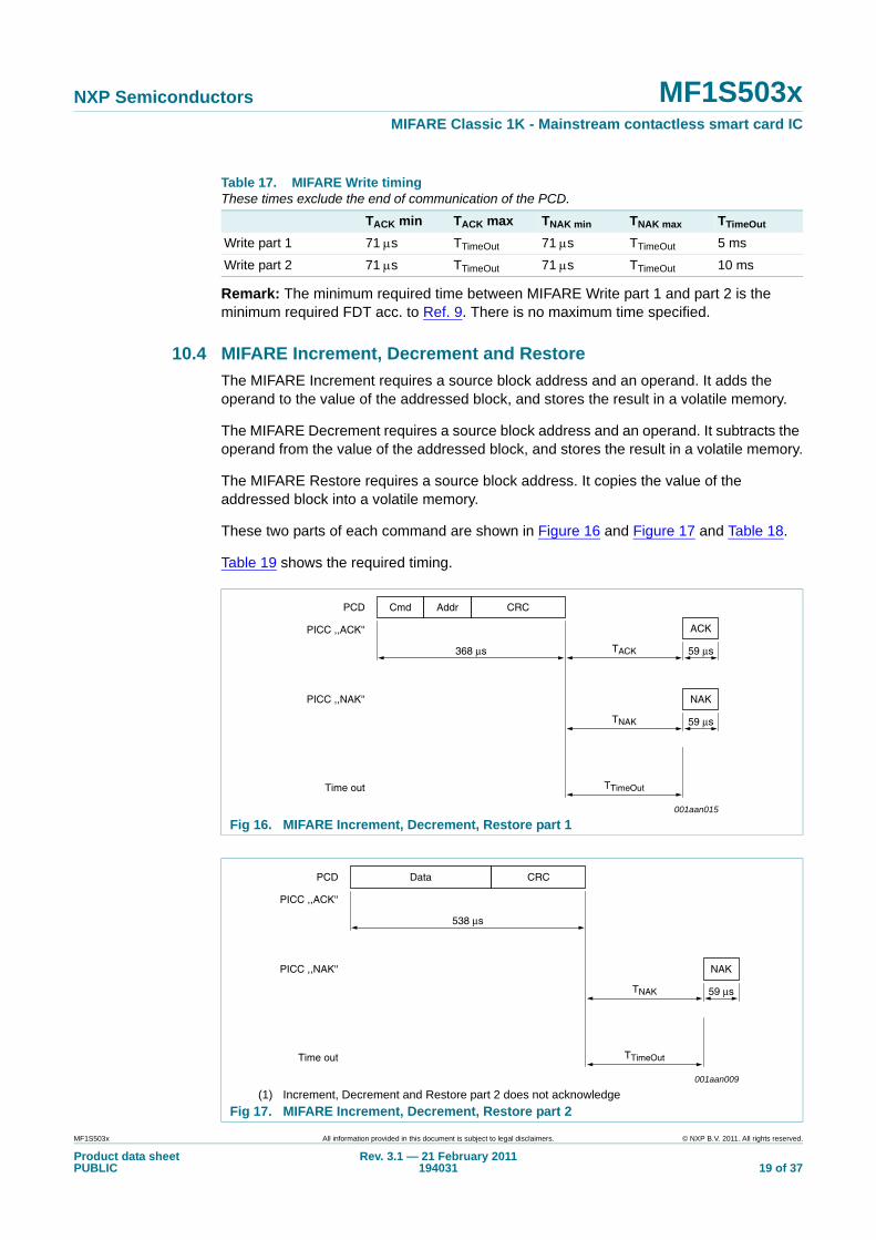
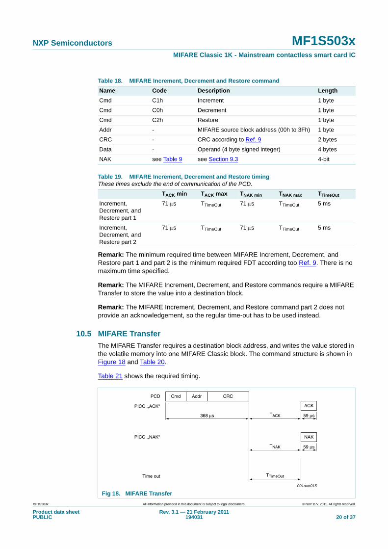
10.4 MIFARE Increment, Decrement and RestoreThe MIFARE Increment requires a source block address and an operand. It adds the operand to the value of the addressed block, and stores the result in a volatile memory.
The MIFARE Decrement requires a source block address and an operand. It subtracts the operand from the value of the addressed block, and stores the result in a volatile memory.
The MIFARE Restore requires a source block address. It copies the value of the addressed block into a volatile memory.
These two parts of each command are shown in Figure 16 and Figure 17 and Table 18.
Table 19 shows the required timing.
Table 17. MIFARE Write timingThese times exclude the end of communication of the PCD.
TACK min TACK max TNAK min TNAK max TTimeOut
Write part 1 71 μs TTimeOut 71 μs TTimeOut 5 ms
Write part 2 71 μs TTimeOut 71 μs TTimeOut 10 ms
Fig 16. MIFARE Increment, Decrement, Restore part 1
(1) Increment, Decrement and Restore part 2 does not acknowledgeFig 17. MIFARE Increment, Decrement, Restore part 2
001aan015
CRCAddrPCD Cmd
PICC ,,ACK''
368 μs
PICC ,,NAK'' NAK
Time out TTimeOut
TNAK
TACK
59 μs
ACK
59 μs
001aan009
CRCPCD Data
PICC ,,ACK''
538 μs
PICC ,,NAK'' NAK
Time out TTimeOut
TNAK 59 μs
MF1S503x All information provided in this document is subject to legal disclaimers. © NXP B.V. 2011. All rights reserved.
Product data sheetPUBLIC
Rev. 3.1 — 21 February 2011194031 20 of 37
NXP Semiconductors MF1S503xMIFARE Classic 1K - Mainstream contactless smart card IC
Remark: The minimum required time between MIFARE Increment, Decrement, and Restore part 1 and part 2 is the minimum required FDT according too Ref. 9. There is no maximum time specified.
Remark: The MIFARE Increment, Decrement, and Restore commands require a MIFARE Transfer to store the value into a destination block.
Remark: The MIFARE Increment, Decrement, and Restore command part 2 does not provide an acknowledgement, so the regular time-out has to be used instead.
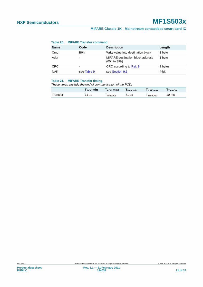
10.5 MIFARE TransferThe MIFARE Transfer requires a destination block address, and writes the value stored in the volatile memory into one MIFARE Classic block. The command structure is shown in Figure 18 and Table 20.
Table 21 shows the required timing.
Table 18. MIFARE Increment, Decrement and Restore commandName Code Description LengthCmd C1h Increment 1 byte
Cmd C0h Decrement 1 byte
Cmd C2h Restore 1 byte
Addr - MIFARE source block address (00h to 3Fh) 1 byte
CRC - CRC according to Ref. 9 2 bytes
Data - Operand (4 byte signed integer) 4 bytes
NAK see Table 9 see Section 9.3 4-bit
Table 19. MIFARE Increment, Decrement and Restore timingThese times exclude the end of communication of the PCD.
TACK min TACK max TNAK min TNAK max TTimeOut
Increment, Decrement, and Restore part 1
71 μs TTimeOut 71 μs TTimeOut 5 ms
Increment, Decrement, and Restore part 2
71 μs TTimeOut 71 μs TTimeOut 5 ms
Fig 18. MIFARE Transfer001aan015
CRCAddrPCD Cmd
PICC ,,ACK''
368 μs
PICC ,,NAK'' NAK
Time out TTimeOut
TNAK
TACK
59 μs
ACK
59 μs
MF1S503x All information provided in this document is subject to legal disclaimers. © NXP B.V. 2011. All rights reserved.
Product data sheetPUBLIC
Rev. 3.1 — 21 February 2011194031 21 of 37
NXP Semiconductors MF1S503xMIFARE Classic 1K - Mainstream contactless smart card IC
Table 20. MIFARE Transfer commandName Code Description LengthCmd B0h Write value into destination block 1 byte
Addr - MIFARE destination block address (00h to 3Fh)
1 byte
CRC - CRC according to Ref. 9 2 bytes
NAK see Table 9 see Section 9.3 4-bit
Table 21. MIFARE Transfer timingThese times exclude the end of communication of the PCD.
TACK min TACK max TNAK min TNAK max TTimeOut
Transfer 71 μs TTimeOut 71 μs TTimeOut 10 ms
MF1S503x All information provided in this document is subject to legal disclaimers. © NXP B.V. 2011. All rights reserved.
Product data sheetPUBLIC
Rev. 3.1 — 21 February 2011194031 22 of 37
NXP Semiconductors MF1S503xMIFARE Classic 1K - Mainstream contactless smart card IC
11. Limiting values
[1] Stresses above one or more of the limiting values may cause permanent damage to the device
[2] Exposure to limiting values for extended periods may affect device reliability
[3] MIL Standard 883-C method 3015; Human body model: C = 100 pF, R = 1.5 kΩ
12. Characteristics
[1] LCR meter, Tamb = 22 °C, fi = 13.56 MHz, 2 V RMS.
Table 22. Limiting values [1][2]
In accordance with the Absolute Maximum Rating System (IEC 60134).
Symbol Parameter Min Max UnitII input current - 30 mA
Ptot/pack total power dissipation per package - 200 mW
Tstg storage temperature −55 125 °C
Tamb ambient temperature −25 70 °C
VESD electrostatic discharge voltage [3] 2 - kV
Table 23. CharacteristicsSymbol Parameter Conditions Min Typ Max UnitCi input capacitance [1] 14.4 16.1 17.4 pF
fi input frequency - 13.56 - MHz
EEPROM characteristicstret retention time Tamb = 22 °C 10 - - year
Nendu(W) write endurance Tamb = 22 °C 100000 200000 - cycle
MF1S503x All information provided in this document is subject to legal disclaimers. © NXP B.V. 2011. All rights reserved.
Product data sheetPUBLIC
Rev. 3.1 — 21 February 2011194031 23 of 37
NXP Semiconductors MF1S503xMIFARE Classic 1K - Mainstream contactless smart card IC
13. Wafer specification
For more details on the wafer delivery forms see Ref. 6.
[1] the gap between chips may vary due to changing foil expansion
Table 24. Wafer specifications MF1S5035DUx/LWaferdiameter 200 mm typical (8 inches)
maximum diameter after foil expansion 210 mm
thickness 120 μm ± 15 μm
flatness not applicable
Potential Good Dies per Wafer (PGDW) 27720
Wafer backsidematerial Si
treatment ground and stress relieveroughness Ra max = 0.5 μm
Rt max = 5 μm
Chip dimensionsstep size x = 1062 μm
y = 1012 μm
gap between chips[1] typical = 27 μm
minimum = 5 μm
Passivationtype sandwich structure
material PSG / nitride
thickness 500 nm / 600 nm
Table 25. Wafer specifications MF1S5037DUxWaferdiameter 200 mm typical (8 inches)
thickness 120 μm ± 15 μm
flatness not applicable
Potential Good Dies per Wafer (PGDW) 25060
Wafer backsidematerial Si
treatment ground and stress relieveroughness Ra max = 0.5 μm
Rt max = 5 μm
Chip dimensionsstep size x = 1100 μm
y = 1030 μm
scribe line x = 86,4 μm
y = 66,4 μm
MF1S503x All information provided in this document is subject to legal disclaimers. © NXP B.V. 2011. All rights reserved.
Product data sheetPUBLIC
Rev. 3.1 — 21 February 2011194031 24 of 37
NXP Semiconductors MF1S503xMIFARE Classic 1K - Mainstream contactless smart card IC
[1] the gap between chips may vary due to changing foil expansion
[1] Pads VSS and TESTIO are disconnected when wafer is sawn.
[1] Pads VSS and TESTIO are disconnected when wafer is sawn.
13.1 Fail die identificationElectronic wafer mapping covers the electrical test results and additionally the results of mechanical/visual inspection.
No ink dots are applied.
Passivationtype sandwich structure
material PSG / nitride
thickness 500 nm / 600 nm
Table 26. Bond pad specificationsBond pads (substrate connected to VSS)size (metallization) LA, LB, VSS[1] = 118 μm × 118 μm
TESTIO[1] = 103 μm × 118 μm
size (pad opening) LA, LB, VSS[1] = 90 μm × 90 μm
TESTIO[1] = 75 μm × 90 μm
material Al-Cu
thickness 850 nm
Table 27. Bump specificationsAu bump (substrate connected to VSS)material > 99.9 % pure Au
hardness 35 to 80 HV 0.005
shear strength > 70 MPa
height 18 μm
height uniformity within a die = ±2 μm
within a wafer = ±3 μm
wafer to wafer = ±4 μm
flatness minimum = ±1.5 μm
size LA, LB, VSS[1] = 104 μm × 104 μm
TESTIO[1] = 89 μm × 104 μm
size variation ±5 μm
under bump metallization sputtered TiW
Table 25. Wafer specifications MF1S5037DUx …continued
MF1S503x All information provided in this document is subject to legal disclaimers. © NXP B.V. 2011. All rights reserved.
Product data sheetPUBLIC
Rev. 3.1 — 21 February 2011194031 25 of 37
NXP Semiconductors MF1S503xMIFARE Classic 1K - Mainstream contactless smart card IC
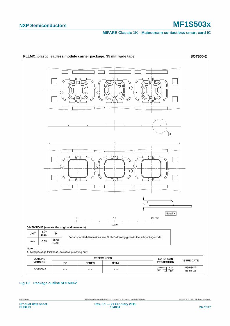
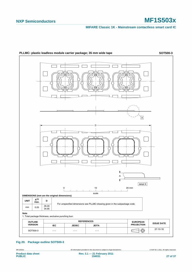
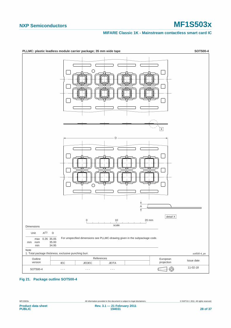
14. Package outline
For more details on the contactless modules MOA2, MOA4, MOA8 and MOB6 please refer to Ref. 2, Ref. 3, Ref. 4 and Ref. 5.
MF1S503x All information provided in this document is subject to legal disclaimers. © NXP B.V. 2011. All rights reserved.
Product data sheetPUBLIC
Rev. 3.1 — 21 February 2011194031 26 of 37
NXP Semiconductors MF1S503xMIFARE Classic 1K - Mainstream contactless smart card IC
Fig 19. Package outline SOT500-2
UNIT D
REFERENCESOUTLINEVERSION
EUROPEANPROJECTION ISSUE DATE
IEC JEDEC JEITA
mm 35.0534.95
For unspecified dimensions see PLLMC-drawing given in the subpackage code.
DIMENSIONS (mm are the original dimensions)
SOT500-203-09-1706-05-22- - - - - -- - -
PLLMC: plastic leadless module carrier package; 35 mm wide tape SOT500-2
A(1)
max.
0.33
0 10 20 mm
scale
A
detail X
X
Note1. Total package thickness, exclusive punching burr.
D
MF1S503x All information provided in this document is subject to legal disclaimers. © NXP B.V. 2011. All rights reserved.
Product data sheetPUBLIC
Rev. 3.1 — 21 February 2011194031 27 of 37
NXP Semiconductors MF1S503xMIFARE Classic 1K - Mainstream contactless smart card IC
Fig 20. Package outline SOT500-3
UNIT D
REFERENCESOUTLINEVERSION
EUROPEANPROJECTION ISSUE DATE
IEC JEDEC JEITA
mm 35.0534.95
For unspecified dimensions see PLLMC-drawing given in the subpackage code.
DIMENSIONS (mm are the original dimensions)
SOT500-307-10-18
- - - - - -- - -
PLLMC: plastic leadless module carrier package; 35 mm wide tape SOT500-3
A(1)
max.
0.25
0 10 20 mm
scale
A
detail X
X
Note1. Total package thickness, exclusive punching burr.
D
MF1S503x All information provided in this document is subject to legal disclaimers. © NXP B.V. 2011. All rights reserved.
Product data sheetPUBLIC
Rev. 3.1 — 21 February 2011194031 28 of 37
NXP Semiconductors MF1S503xMIFARE Classic 1K - Mainstream contactless smart card IC
Fig 21. Package outline SOT500-4
ReferencesOutlineversion
Europeanprojection Issue date
IEC JEDEC JEITA
SOT500-4 - - -- - -- - -
sot500-4_po
11-02-18
Unit
mmmaxnommin
0.26 35.0535.0034.95
A(1)
Dimensions
Note1. Total package thickness, exclusive punching burr.
PLLMC: plastic leadless module carrier package; 35 mm wide tape SOT500-4
D
For unspecified dimensions see PLLMC-drawing given in the subpackage code.
0 10 20 mm
scale
X
D
detail X
A
MF1S503x All information provided in this document is subject to legal disclaimers. © NXP B.V. 2011. All rights reserved.
Product data sheetPUBLIC
Rev. 3.1 — 21 February 2011194031 29 of 37
NXP Semiconductors MF1S503xMIFARE Classic 1K - Mainstream contactless smart card IC
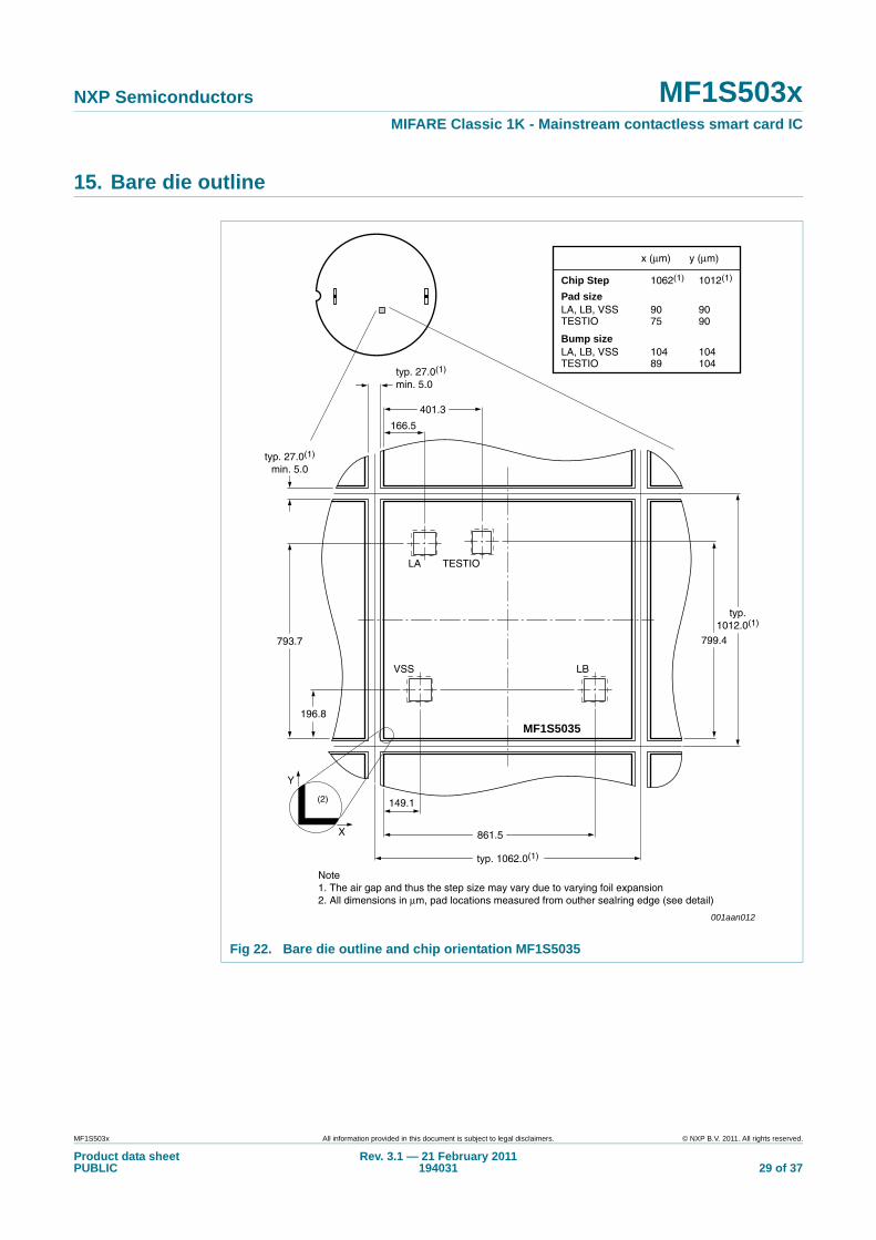
15. Bare die outline
Fig 22. Bare die outline and chip orientation MF1S5035
001aan012
VSS
LA TESTIO
LB
Chip Step
LA, LB, VSSTESTIO
9075
90
x (μm) y (μm)
90
LA, LB, VSSTESTIO
10489
104104
1062(1) 1012(1)
Y
X
typ. 27.0(1)
min. 5.0
793.7
196.8
166.5
401.3
149.1
861.5
typ. 1062.0(1)
typ.1012.0(1)
799.4
typ. 27.0(1)
min. 5.0
Note1. The air gap and thus the step size may vary due to varying foil expansion2. All dimensions in μm, pad locations measured from outher sealring edge (see detail)
(2)
MF1S5035
Pad size
Bump size
MF1S503x All information provided in this document is subject to legal disclaimers. © NXP B.V. 2011. All rights reserved.
Product data sheetPUBLIC
Rev. 3.1 — 21 February 2011194031 30 of 37
NXP Semiconductors MF1S503xMIFARE Classic 1K - Mainstream contactless smart card IC
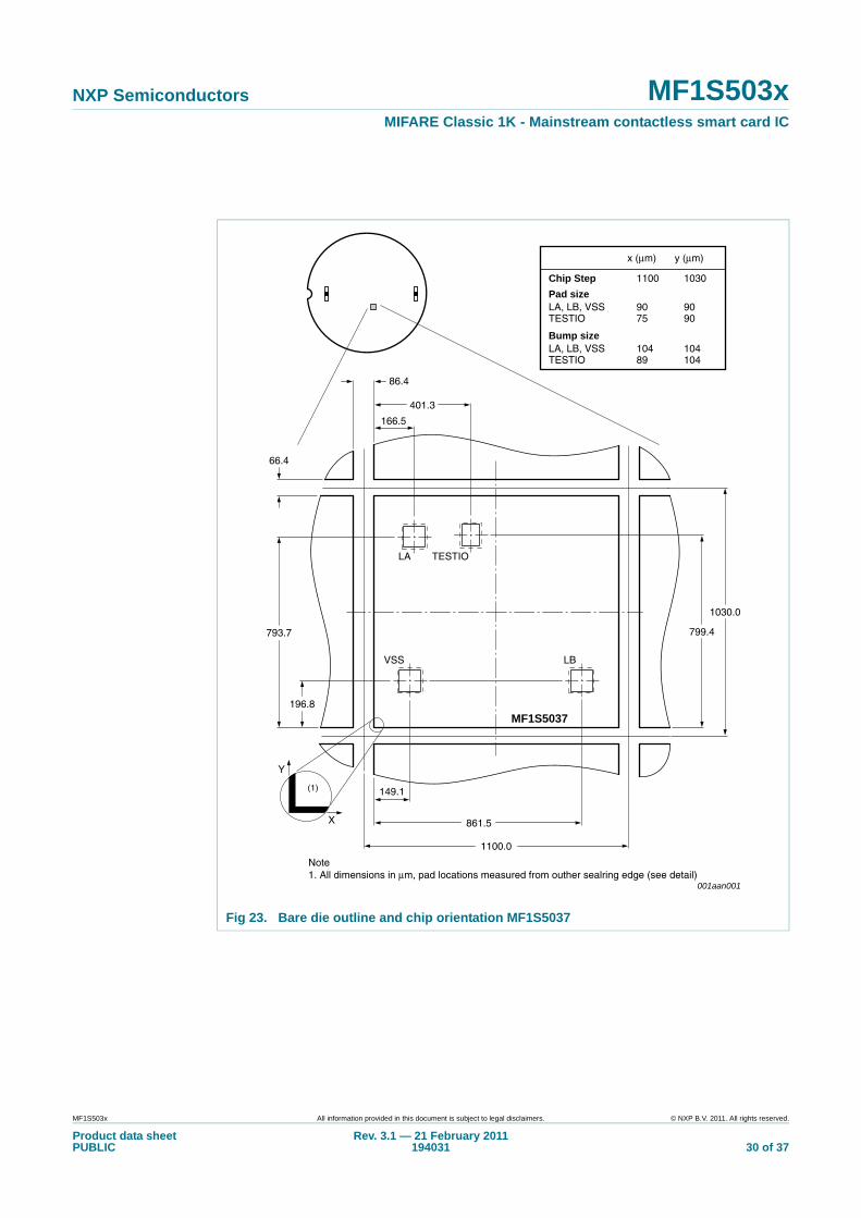
Fig 23. Bare die outline and chip orientation MF1S5037
001aan001
VSS
LA TESTIO
LB
MF1S5037
Chip Step
Pad sizeLA, LB, VSS
Bump size
TESTIO9075
90
x (μm) y (μm)
90
LA, LB, VSSTESTIO
10489
104104
1100 1030
86.4
Y
X
66.4
793.7
196.8
166.5
401.3
149.1
861.5
1100.0
Note1. All dimensions in μm, pad locations measured from outher sealring edge (see detail)
(1)
1030.0
799.4
MF1S503x All information provided in this document is subject to legal disclaimers. © NXP B.V. 2011. All rights reserved.
Product data sheetPUBLIC
Rev. 3.1 — 21 February 2011194031 31 of 37
NXP Semiconductors MF1S503xMIFARE Classic 1K - Mainstream contactless smart card IC
16. Abbreviations
Table 28. Abbreviations and symbolsAcronym DescriptionACK ACKnowledge
ATQA Answer To reQuest, Type A
CRC Cyclic Redundancy Check
EEPROM Electrically Erasable Programmable Read-Only Memory
FDT Frame Delay Time
FFC Film Frame Carrier
IC Integrated Circuit
LCR L = inductance, Capacitance, Resistance (LCR meter)
LSB Least Significant Bit
NAK Not AcKnowledge
NUID Non-Unique IDentifier
PCD Proximity Coupling Device (Contactless Reader)
PICC Proximity Integrated Circuit Card (Contactless Card)
POR Power-On Reset
REQA REQuest command, Type A
RF Radio Frequency
RMS Root Mean Square
SAK Select AcKnowledge, type A
SECS-II SEMI Equipment Communications Standard part 2
TiW Titanium Tungsten
WUPA Wake-Up Protocol type A
MF1S503x All information provided in this document is subject to legal disclaimers. © NXP B.V. 2011. All rights reserved.
Product data sheetPUBLIC
Rev. 3.1 — 21 February 2011194031 32 of 37
NXP Semiconductors MF1S503xMIFARE Classic 1K - Mainstream contactless smart card IC
17. References
[1] MIFARE (Card) Coil Design Guide — Application note, BU-ID Document number 0117**1
[2] Contactless smart card module specification MOA2 — Delivery Type Description, BU-ID Document number 0287**1
[3] Contactless smart card module specification MOA4 — Delivery Type Description, BU-ID Document number 0823**1
[4] Contactless smart card module specification MOA8 — Delivery Type Description, BU-ID Document number 1636**1
[5] Contactless smart card module specification MOB6 — Delivery Type Description, BU-ID Document number 1309**1
[6] General specification for 8" wafer on UV-tape; delivery types — Delivery Type Description, BU-ID Document number 1005**1
[7] MIFARE Type Identification Procedure — Application note, BU-ID Document number 0184**1
[8] ISO/IEC 14443-2 — 2001[9] ISO/IEC 14443-3 — 2001 [10] CLRC632 Multiple protocol contactless reader IC (MIFARE/ICODE1) — Product
data sheet, BU-ID Document number 0739**1
[11] MIFARE and handling of UIDs — Application note, BU-ID Document number 1907**1
1. ** ... document version number
MF1S503x All information provided in this document is subject to legal disclaimers. © NXP B.V. 2011. All rights reserved.
Product data sheetPUBLIC
Rev. 3.1 — 21 February 2011194031 33 of 37
NXP Semiconductors MF1S503xMIFARE Classic 1K - Mainstream contactless smart card IC
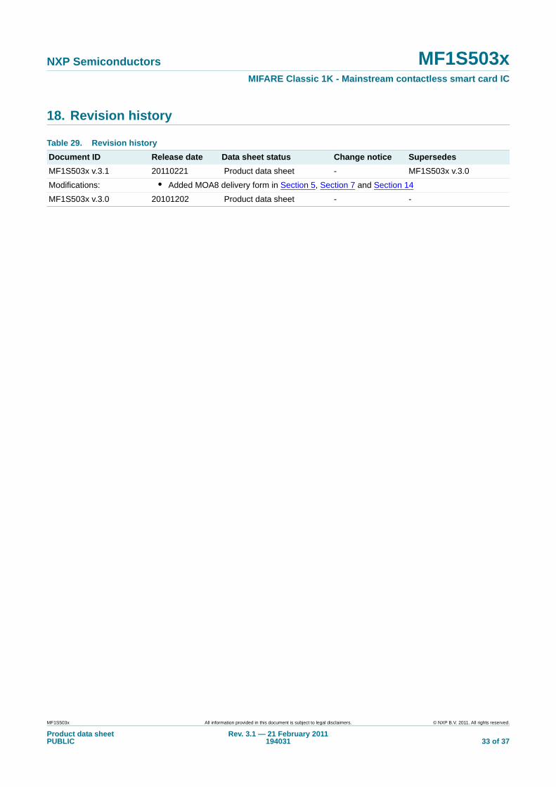
18. Revision history
Table 29. Revision historyDocument ID Release date Data sheet status Change notice SupersedesMF1S503x v.3.1 20110221 Product data sheet - MF1S503x v.3.0
Modifications: • Added MOA8 delivery form in Section 5, Section 7 and Section 14
MF1S503x v.3.0 20101202 Product data sheet - -
MF1S503x All information provided in this document is subject to legal disclaimers. © NXP B.V. 2011. All rights reserved.
Product data sheetPUBLIC
Rev. 3.1 — 21 February 2011194031 34 of 37
NXP Semiconductors MF1S503xMIFARE Classic 1K - Mainstream contactless smart card IC
19. Legal information
19.1 Data sheet status
[1] Please consult the most recently issued document before initiating or completing a design.
[2] The term ‘short data sheet’ is explained in section “Definitions”.
[3] The product status of device(s) described in this document may have changed since this document was published and may differ in case of multiple devices. The latest product status information is available on the Internet at URL http://www.nxp.com.
19.2 DefinitionsDraft — The document is a draft version only. The content is still under internal review and subject to formal approval, which may result in modifications or additions. NXP Semiconductors does not give any representations or warranties as to the accuracy or completeness of information included herein and shall have no liability for the consequences of use of such information.
Short data sheet — A short data sheet is an extract from a full data sheet with the same product type number(s) and title. A short data sheet is intended for quick reference only and should not be relied upon to contain detailed and full information. For detailed and full information see the relevant full data sheet, which is available on request via the local NXP Semiconductors sales office. In case of any inconsistency or conflict with the short data sheet, the full data sheet shall prevail.
Product specification — The information and data provided in a Product data sheet shall define the specification of the product as agreed between NXP Semiconductors and its customer, unless NXP Semiconductors and customer have explicitly agreed otherwise in writing. In no event however, shall an agreement be valid in which the NXP Semiconductors product is deemed to offer functions and qualities beyond those described in the Product data sheet.
19.3 DisclaimersLimited warranty and liability — Information in this document is believed to be accurate and reliable. However, NXP Semiconductors does not give any representations or warranties, expressed or implied, as to the accuracy or completeness of such information and shall have no liability for the consequences of use of such information.
In no event shall NXP Semiconductors be liable for any indirect, incidental, punitive, special or consequential damages (including - without limitation - lost profits, lost savings, business interruption, costs related to the removal or replacement of any products or rework charges) whether or not such damages are based on tort (including negligence), warranty, breach of contract or any other legal theory.
Notwithstanding any damages that customer might incur for any reason whatsoever, NXP Semiconductors’ aggregate and cumulative liability towards customer for the products described herein shall be limited in accordance with the Terms and conditions of commercial sale of NXP Semiconductors.
Right to make changes — NXP Semiconductors reserves the right to make changes to information published in this document, including without limitation specifications and product descriptions, at any time and without notice. This document supersedes and replaces all information supplied prior to the publication hereof.
Suitability for use — NXP Semiconductors products are not designed, authorized or warranted to be suitable for use in life support, life-critical or safety-critical systems or equipment, nor in applications where failure or
malfunction of an NXP Semiconductors product can reasonably be expected to result in personal injury, death or severe property or environmental damage. NXP Semiconductors accepts no liability for inclusion and/or use of NXP Semiconductors products in such equipment or applications and therefore such inclusion and/or use is at the customer’s own risk.
Applications — Applications that are described herein for any of these products are for illustrative purposes only. NXP Semiconductors makes no representation or warranty that such applications will be suitable for the specified use without further testing or modification.
Customers are responsible for the design and operation of their applications and products using NXP Semiconductors products, and NXP Semiconductors accepts no liability for any assistance with applications or customer product design. It is customer’s sole responsibility to determine whether the NXP Semiconductors product is suitable and fit for the customer’s applications and products planned, as well as for the planned application and use of customer’s third party customer(s). Customers should provide appropriate design and operating safeguards to minimize the risks associated with their applications and products.
NXP Semiconductors does not accept any liability related to any default, damage, costs or problem which is based on any weakness or default in the customer’s applications or products, or the application or use by customer’s third party customer(s). Customer is responsible for doing all necessary testing for the customer’s applications and products using NXP Semiconductors products in order to avoid a default of the applications and the products or of the application or use by customer’s third party customer(s). NXP does not accept any liability in this respect.
Limiting values — Stress above one or more limiting values (as defined in the Absolute Maximum Ratings System of IEC 60134) will cause permanent damage to the device. Limiting values are stress ratings only and (proper) operation of the device at these or any other conditions above those given in the Recommended operating conditions section (if present) or the Characteristics sections of this document is not warranted. Constant or repeated exposure to limiting values will permanently and irreversibly affect the quality and reliability of the device.
Quick reference data — The Quick reference data is an extract of the product data given in the Limiting values and Characteristics sections of this document, and as such is not complete, exhaustive or legally binding.
Terms and conditions of commercial sale — NXP Semiconductors products are sold subject to the general terms and conditions of commercial sale, as published at http://www.nxp.com/profile/terms, unless otherwise agreed in a valid written individual agreement. In case an individual agreement is concluded only the terms and conditions of the respective agreement shall apply. NXP Semiconductors hereby expressly objects to applying the customer’s general terms and conditions with regard to the purchase of NXP Semiconductors products by customer.
No offer to sell or license — Nothing in this document may be interpreted or construed as an offer to sell products that is open for acceptance or the grant, conveyance or implication of any license under any copyrights, patents or other industrial or intellectual property rights.
Document status[1][2] Product status[3] Definition
Objective [short] data sheet Development This document contains data from the objective specification for product development.
Preliminary [short] data sheet Qualification This document contains data from the preliminary specification.
Product [short] data sheet Production This document contains the product specification.
MF1S503x All information provided in this document is subject to legal disclaimers. © NXP B.V. 2011. All rights reserved.
Product data sheetPUBLIC
Rev. 3.1 — 21 February 2011194031 35 of 37
NXP Semiconductors MF1S503xMIFARE Classic 1K - Mainstream contactless smart card IC
Export control — This document as well as the item(s) described herein may be subject to export control regulations. Export might require a prior authorization from national authorities.
Non-automotive qualified products — Unless this data sheet expressly states that this specific NXP Semiconductors product is automotive qualified, the product is not suitable for automotive use. It is neither qualified nor tested in accordance with automotive testing or application requirements. NXP Semiconductors accepts no liability for inclusion and/or use of non-automotive qualified products in automotive equipment or applications.
In the event that customer uses the product for design-in and use in automotive applications to automotive specifications and standards, customer (a) shall use the product without NXP Semiconductors’ warranty of the product for such automotive applications, use and specifications, and (b) whenever customer uses the product for automotive applications beyond NXP Semiconductors’ specifications such use shall be solely at customer’s own risk, and (c) customer fully indemnifies NXP Semiconductors for any liability, damages or failed product claims resulting from customer design and use of the product for automotive applications beyond NXP Semiconductors’ standard warranty and NXP Semiconductors’ product specifications.
Bare die — All die are tested on compliance with their related technical specifications as stated in this data sheet up to the point of wafer sawing and are handled in accordance with the NXP Semiconductors storage and transportation conditions. If there are data sheet limits not guaranteed, these will be separately indicated in the data sheet. There are no post-packing tests performed on individual die or wafers.
NXP Semiconductors has no control of third party procedures in the sawing, handling, packing or assembly of the die. Accordingly, NXP Semiconductors assumes no liability for device functionality or performance of the die or systems after third party sawing, handling, packing or assembly of the die. It is the responsibility of the customer to test and qualify their application in which the die is used.
All die sales are conditioned upon and subject to the customer entering into a written die sale agreement with NXP Semiconductors through its legal department.
19.4 TrademarksNotice: All referenced brands, product names, service names and trademarks are the property of their respective owners.
MIFARE — is a trademark of NXP B.V.
20. Contact information
For more information, please visit: http://www.nxp.com
For sales office addresses, please send an email to: [email protected]
MF1S503x All information provided in this document is subject to legal disclaimers. © NXP B.V. 2011. All rights reserved.
Product data sheetPUBLIC
Rev. 3.1 — 21 February 2011194031 36 of 37
NXP Semiconductors MF1S503xMIFARE Classic 1K - Mainstream contactless smart card IC
21. Tables
Table 1. Quick reference data . . . . . . . . . . . . . . . . . . . . .2Table 2. Ordering information . . . . . . . . . . . . . . . . . . . . .3Table 3. Pin allocation table . . . . . . . . . . . . . . . . . . . . . . .4Table 4. Memory operations. . . . . . . . . . . . . . . . . . . . . . 11Table 5. Access conditions. . . . . . . . . . . . . . . . . . . . . . . 11Table 6. Access conditions for the sector trailer . . . . . .12Table 7. Access conditions for data blocks. . . . . . . . . . .13Table 8. Command overview . . . . . . . . . . . . . . . . . . . . .14Table 9. MIFARE ACK and NAK . . . . . . . . . . . . . . . . . .15Table 10. ATQA response of the MF1S503x . . . . . . . . . .15Table 11. SAK response of the MF1S503x . . . . . . . . . . .15Table 12. MIFARE authentication command . . . . . . . . . .16Table 13. MIFARE authentication timing . . . . . . . . . . . . .17Table 14. MIFARE Read command . . . . . . . . . . . . . . . . .17Table 15. MIFARE Read timing . . . . . . . . . . . . . . . . . . . .17Table 16. MIFARE Write command . . . . . . . . . . . . . . . . .18
Table 17. MIFARE Write timing . . . . . . . . . . . . . . . . . . . . 19Table 18. MIFARE Increment, Decrement and
Restore command . . . . . . . . . . . . . . . . . . . . . . 20Table 19. MIFARE Increment, Decrement and
Restore timing . . . . . . . . . . . . . . . . . . . . . . . . . 20Table 20. MIFARE Transfer command. . . . . . . . . . . . . . . 21Table 21. MIFARE Transfer timing. . . . . . . . . . . . . . . . . . 21Table 22. Limiting values [1][2] . . . . . . . . . . . . . . . . . . . . . 22Table 23. Characteristics . . . . . . . . . . . . . . . . . . . . . . . . 22Table 24. Wafer specifications MF1S5035DUx/L . . . . . . 23Table 25. Wafer specifications MF1S5037DUx . . . . . . . 23Table 26. Bond pad specifications . . . . . . . . . . . . . . . . . . 24Table 27. Bump specifications . . . . . . . . . . . . . . . . . . . . . 24Table 28. Abbreviations and symbols . . . . . . . . . . . . . . . 31Table 29. Revision history . . . . . . . . . . . . . . . . . . . . . . . . 33
22. Figures
Fig 1. MIFARE card reader . . . . . . . . . . . . . . . . . . . . . . .1Fig 2. Block diagram of MF1S503x . . . . . . . . . . . . . . . . .3Fig 3. Pin configuration for SOT500-2 (MOA4) . . . . . . . .4Fig 4. Three pass authentication . . . . . . . . . . . . . . . . . . .6Fig 5. Memory organization . . . . . . . . . . . . . . . . . . . . . . .8Fig 6. Manufacturer block . . . . . . . . . . . . . . . . . . . . . . . .9Fig 7. Value blocks. . . . . . . . . . . . . . . . . . . . . . . . . . . . . .9Fig 8. Sector trailer . . . . . . . . . . . . . . . . . . . . . . . . . . . .10Fig 9. Access conditions . . . . . . . . . . . . . . . . . . . . . . . .12Fig 10. Frame Delay Time (from PCD to PICC)
and TACK and TNAK. . . . . . . . . . . . . . . . . . . . . . . .15Fig 11. MIFARE Authentication part 1 . . . . . . . . . . . . . . .16Fig 12. MIFARE Authentication part 2 . . . . . . . . . . . . . . .16Fig 13. MIFARE Read . . . . . . . . . . . . . . . . . . . . . . . . . . .17Fig 14. MIFARE Write part 1 . . . . . . . . . . . . . . . . . . . . . .18Fig 15. MIFARE Write part 2 . . . . . . . . . . . . . . . . . . . . . .18Fig 16. MIFARE Increment, Decrement,
Restore part 1 . . . . . . . . . . . . . . . . . . . . . . . . . . .19Fig 17. MIFARE Increment, Decrement,
Restore part 2 . . . . . . . . . . . . . . . . . . . . . . . . . . .19Fig 18. MIFARE Transfer . . . . . . . . . . . . . . . . . . . . . . . . .20Fig 19. Package outline SOT500-2 . . . . . . . . . . . . . . . . .26Fig 20. Package outline SOT500-3 . . . . . . . . . . . . . . . . .27Fig 21. Package outline SOT500-4 . . . . . . . . . . . . . . . . .28Fig 22. Bare die outline and chip orientation
MF1S5035 . . . . . . . . . . . . . . . . . . . . . . . . . . . . . .29Fig 23. Bare die outline and chip orientation
MF1S5037 . . . . . . . . . . . . . . . . . . . . . . . . . . . . . .30
NXP Semiconductors MF1S503xMIFARE Classic 1K - Mainstream contactless smart card IC
© NXP B.V. 2011. All rights reserved.For more information, please visit: http://www.nxp.comFor sales office addresses, please send an email to: [email protected]
Date of release: 21 February 2011194031
Please be aware that important notices concerning this document and the product(s)described herein, have been included in section ‘Legal information’.
23. Contents
1 General description . . . . . . . . . . . . . . . . . . . . . . 11.1 Anti-collision . . . . . . . . . . . . . . . . . . . . . . . . . . . 11.2 Simple integration and user convenience. . . . . 11.3 Security. . . . . . . . . . . . . . . . . . . . . . . . . . . . . . . 11.4 Delivery options . . . . . . . . . . . . . . . . . . . . . . . . 12 Features and benefits . . . . . . . . . . . . . . . . . . . . 22.1 EEPROM . . . . . . . . . . . . . . . . . . . . . . . . . . . . . 23 Applications . . . . . . . . . . . . . . . . . . . . . . . . . . . . 24 Quick reference data . . . . . . . . . . . . . . . . . . . . . 25 Ordering information. . . . . . . . . . . . . . . . . . . . . 36 Block diagram . . . . . . . . . . . . . . . . . . . . . . . . . . 37 Pinning information. . . . . . . . . . . . . . . . . . . . . . 47.1 Pinning . . . . . . . . . . . . . . . . . . . . . . . . . . . . . . . 48 Functional description . . . . . . . . . . . . . . . . . . . 58.1 Block description . . . . . . . . . . . . . . . . . . . . . . . 58.2 Communication principle . . . . . . . . . . . . . . . . . 58.2.1 Request standard/all. . . . . . . . . . . . . . . . . . . . . 58.2.2 Anti-collision loop . . . . . . . . . . . . . . . . . . . . . . . 58.2.3 Select card . . . . . . . . . . . . . . . . . . . . . . . . . . . . 68.2.4 Three pass authentication . . . . . . . . . . . . . . . . 68.2.5 Memory operations. . . . . . . . . . . . . . . . . . . . . . 78.3 Data integrity. . . . . . . . . . . . . . . . . . . . . . . . . . . 78.4 Three pass authentication sequence . . . . . . . . 78.5 RF interface . . . . . . . . . . . . . . . . . . . . . . . . . . . 88.6 Memory organization . . . . . . . . . . . . . . . . . . . . 88.6.1 Manufacturer block . . . . . . . . . . . . . . . . . . . . . . 98.6.2 Data blocks. . . . . . . . . . . . . . . . . . . . . . . . . . . . 98.6.2.1 Value blocks . . . . . . . . . . . . . . . . . . . . . . . . . . . 98.6.3 Sector trailer (block 3) . . . . . . . . . . . . . . . . . . 108.7 Memory access . . . . . . . . . . . . . . . . . . . . . . . 118.7.1 Access conditions. . . . . . . . . . . . . . . . . . . . . . 118.7.2 Access conditions for the sector trailer . . . . . . 128.7.3 Access conditions for data blocks. . . . . . . . . . 139 Command overview. . . . . . . . . . . . . . . . . . . . . 149.1 MIFARE Classic command overview . . . . . . . 149.2 Timings . . . . . . . . . . . . . . . . . . . . . . . . . . . . . . 149.3 MIFARE Classic ACK and NAK . . . . . . . . . . . 159.4 ATQA and SAK responses . . . . . . . . . . . . . . . 1510 MIFARE Classic commands . . . . . . . . . . . . . . 1610.1 MIFARE Authentication . . . . . . . . . . . . . . . . . 1610.2 MIFARE Read. . . . . . . . . . . . . . . . . . . . . . . . . 1710.3 MIFARE Write . . . . . . . . . . . . . . . . . . . . . . . . . 1810.4 MIFARE Increment, Decrement and Restore . 1910.5 MIFARE Transfer . . . . . . . . . . . . . . . . . . . . . . 2011 Limiting values. . . . . . . . . . . . . . . . . . . . . . . . . 22
12 Characteristics . . . . . . . . . . . . . . . . . . . . . . . . 2213 Wafer specification . . . . . . . . . . . . . . . . . . . . . 2313.1 Fail die identification . . . . . . . . . . . . . . . . . . . 2414 Package outline. . . . . . . . . . . . . . . . . . . . . . . . 2515 Bare die outline . . . . . . . . . . . . . . . . . . . . . . . . 2916 Abbreviations . . . . . . . . . . . . . . . . . . . . . . . . . 3117 References. . . . . . . . . . . . . . . . . . . . . . . . . . . . 3218 Revision history . . . . . . . . . . . . . . . . . . . . . . . 3319 Legal information . . . . . . . . . . . . . . . . . . . . . . 3419.1 Data sheet status . . . . . . . . . . . . . . . . . . . . . . 3419.2 Definitions . . . . . . . . . . . . . . . . . . . . . . . . . . . 3419.3 Disclaimers . . . . . . . . . . . . . . . . . . . . . . . . . . 3419.4 Trademarks . . . . . . . . . . . . . . . . . . . . . . . . . . 3520 Contact information . . . . . . . . . . . . . . . . . . . . 3521 Tables . . . . . . . . . . . . . . . . . . . . . . . . . . . . . . . . 3622 Figures . . . . . . . . . . . . . . . . . . . . . . . . . . . . . . . 3623 Contents. . . . . . . . . . . . . . . . . . . . . . . . . . . . . . 37
Mouser Electronics
Authorized Distributor
Click to View Pricing, Inventory, Delivery & Lifecycle Information: NXP:
MF1S5030DA8,118
Related Documents