Method for Evaluating ICT Probe Penetrability of Flux Residues Karen Tellefsen Alpha Metals Mark Weiss Motorola APEX 2001 / San Diego / January 2001

Welcome message from author
This document is posted to help you gain knowledge. Please leave a comment to let me know what you think about it! Share it to your friends and learn new things together.
Transcript

Method for EvaluatingICT Probe Penetrability
of Flux ResiduesKaren Tellefsen
Alpha Metals
Mark WeissMotorola
APEX 2001 / San Diego / January 2001

Introduction• Printed wiring boards are getting smaller and
increasingly densely populated.• ICT probing is sometimes done on soldered joints
covered with solder paste flux residue.– Tough or hard residue may prevent pin from making
good electrical contact with the soldered joint
• Solder pad size and shape and ICT probe tip shape and for also affect pin penetrability
• There is a need for a test to evaluate ICT probe penetrability.
Past Work• Mackie, and later Guo et al., measured force-to-
contact. – Indication of the relative penetrability of flux residues.– Small number of contacts measured.
• Seelig and Suraski measured the contact resistance of several types of ICT probes to a single type of flat SMT pad soldered with different solder pastes.– Saw flux build-up on ICT probes.

Current Method• Modified automated dispensing machine
– Allows thousands of accurate ICT probes– Different kinds of soldered pads.– Measures resistance – Enhancement of Motorola’s Initial method.
• ICT pin probe-ability studied for:– various solder pastes– solder reflow conditions– solder pad shapes– ICT probe tip shape and pin force

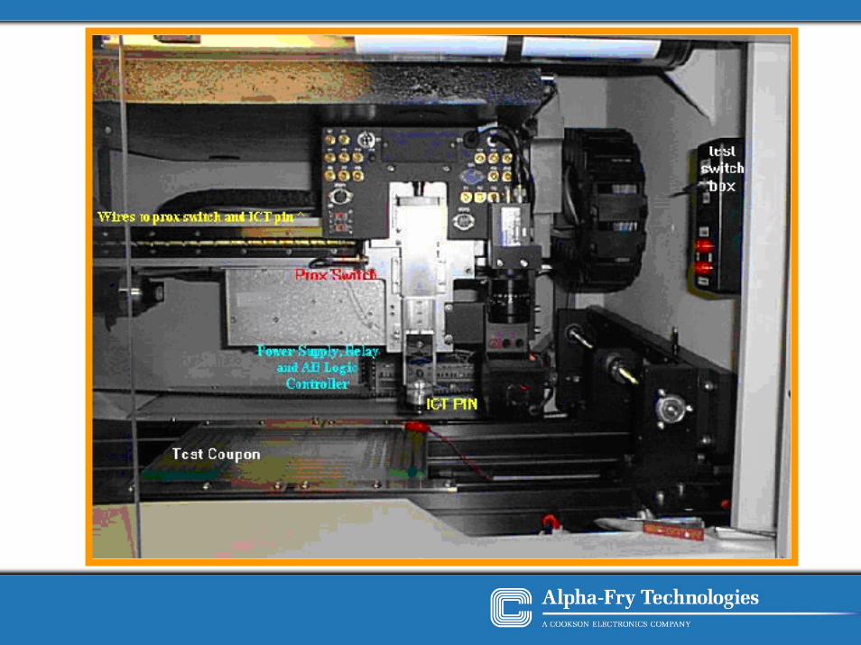
Description of test method• Modified Camalot 3800 Dispensing System
– high-speed, accurate x-y table with a z-axis head with excellent vision system
– small metal ICT socket holds a QA type-100 spring-loaded ICT pin probe
– programmed to allow the ICT pin to accurately and sequentially hit thousands of soldered pads
– z-axis control is set so that the pin is depressed in accordance with the pin specification and exerts the same force for all probe contacts.


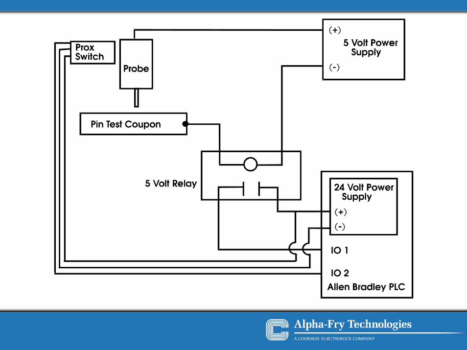
Description of test method• Motorola measurement circuit
– only evaluated circuit continuity– indicates continuity by activating a 5V relay
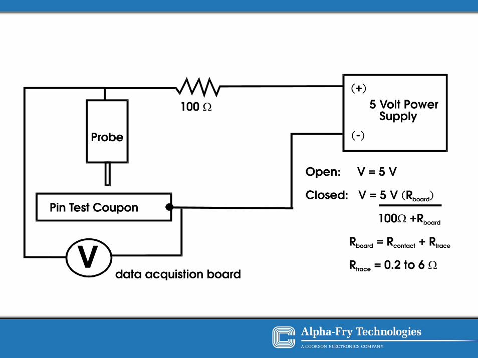
• Contact resistance measurement circuit– Simple voltage divider– measures voltage drop across contact resistance– data acquisition system (National Instruments PC-516
DAQ card programmed with LabView software)– Resistance calculated and stored in ASCII file for
import into spreadsheet.

Description of test method• Test Coupon
– 4032 SMT soldered pads, 1008 each of four types:• A pads, 40 mil squares• B pads, 40 mil squares with 13 mil vias• C pads, 28 mil circles• D pads, 28 mil circles with 13 mil vias
– Connected in series by a single copper trace.• intrinsic resistance of about 5 – 6 Ω• small board resistance correction • contact resistance to an accuracy of ± 0.5 ohms.
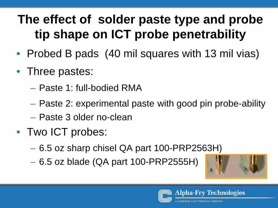
The effect of solder paste type and probe tip shape on ICT probe penetrability
• Probed B pads (40 mil squares with 13 mil vias)• Three pastes:
– Paste 1: full-bodied RMA
– Paste 2: experimental paste with good pin probe-ability– Paste 3 older no-clean
• Two ICT probes:– 6.5 oz sharp chisel QA part 100-PRP2563H)– 6.5 oz blade (QA part 100-PRP2555H)
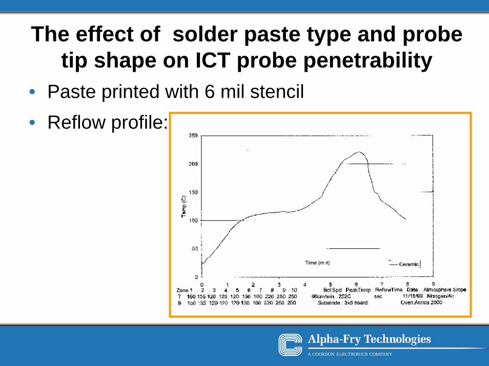
The effect of solder paste type and probe tip shape on ICT probe penetrability
• Paste printed with 6 mil stencil• Reflow profile:

ICT probe-pad resistances for three types of solder paste and two types of probe tips.
Number of probe-pad contactsRange of Chisel-Tipped Pin Blade-Tipped PinResistances Bare Board Paste 1 Paste 2 Paste 3 Paste 1 Paste 2 Paste 3<5 1008 47 863 322 255 1003 3565-10 0 6 14 39 1 2 910-20 0 1 6 15 0 0 020-50 0 2 4 13 0 1 350-100 0 0 2 3 0 0 1100-200 0 0 0 0 0 0 0200-500 0 0 1 8 0 0 3500-1000 0 0 2 1 0 0 01000-2000 0 1 0 0 0 0 1>2000 0 951 116 607 752 2 635

<5 5-10 10-20 20-50 50-100
100-200
200-500
500-1000
1000-2000
>2000
Bare Board
C – Paste 1
C – Paste 2
C – Paste 3
B – Paste 1
B – Paste 2
B – Paste 3
0
200
400
600
800
1000
# Values
Range of ResistancesOhms
Paste
Pin Test Resistances
C = ChiselB = Blade
ICT probe-pad resistances for three types of solder paste and two types of probe tips.

In summary:
• The contact resistance test method can differentiate between solder pastes that are easy to pin test and those that are difficult.
• The contact resistance test method can differentiate between the penetrability of different ICT pins. A probe with a chisel-shaped tip pierced flux residue moderately poorly, while one with a blade-shaped tip pierced flux residues relatively well.

The effect of reflow profile and soldered pad shape on the ICT probe penetrability
• Experimental paste, relatively pin-testable• Printed with 5 mil stencil• 4 reflow conditions• 6.5 oz sharp chisel tipped ICT pin• examined microscopically after 5, 20, 100, and
1008 ICT probes• contact resistances were measured for all four
types of pads

Solder Reflow Conditions Studied
Reflowcondition
PeakTemperature
Soak Time Time aboveLiquidus
1 215°C 90 s 60 s2 215°C 90 s 90 s3 230°C 90 s 60 s4 230°C 90 s 90 s


ICT probe penetrability vs. solder pad shape
Number of Contacts < 5 ΩReflow Profile A B C D
215°C/ 90 s soak / 60 s liq 1008 508 1008 706
215°C/ 90 s soak / 90 s liq 1008 882 1008 630
230°C/ 90 s soak / 60 s liq 1008 869 1008 437
230°C/ 90 s soak / 90 s liq 1008 821 1008 511

In summary:• Soldered pads with vias that trap flux residues are
harder to probe with ICT pins than flat pads.• Some solder paste residues are stickier than other
residues, allowing the residue to be picked up by the probe tip. The built-up flux residues may prevent effective probe-pin electrical contacts if not cleaned with sufficient frequency.
• Reflow conditions affect the hardness of residues. Hotter reflow profiles gives less sticky flux residues, possibly more pin penetrable. However, too hot a reflow profile may render flux residues too hard or tough and less penetrable.

The effect of pin force and number of reflow profiles on ICT probe penetrability
• Experimental paste, relatively pin-testable• Reflowed one or two times• Three coupons for each reflow condition:
– 6.5 oz sharp chisel ICT probes – 10.8 oz sharp chisel probes
• Contact resistances were measured for all four types of pads

Reflow Profile
Entek 220 Pin
0.0
50.0
100.0
150.0
200.0
250.0
0 1 2 3 4 5 6Time (min)
Tem
p (C
)
T1 (C) T2 (C) T3 (C)
Zone 1 2 3 4 5 6 7 8 9 10 BeltSpd PeakTemp Reflow Time Date Atmosphere Slope T 80 100 120 130 150 180 200 218 260 270 105cm/min 225C 46 sec 3/23/99 Air B 80 100 120 130 150 180 200 218 260 270 Substrate : Motorola Pin No Comp; Oven:Atmos 2000
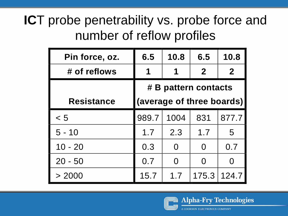
ICT probe penetrability vs. probe force and number of reflow profiles
Pin force, oz. 6.5 10.8 6.5 10.8# of reflows 1 1 2 2
Resistance# B pattern contacts
(average of three boards)
< 5 989.7 1004 831 877.7
5 - 10 1.7 2.3 1.7 5
10 - 20 0.3 0 0 0.7
20 - 50 0.7 0 0 0
> 2000 15.7 1.7 175.3 124.7
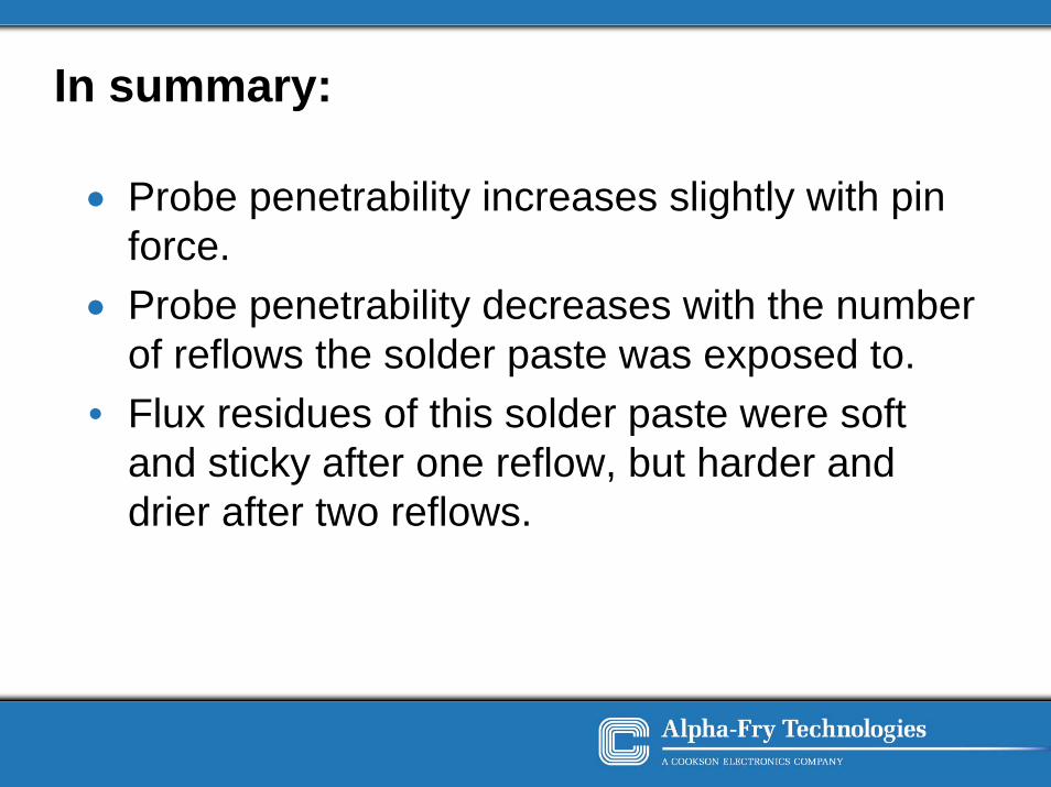
In summary:
• Probe penetrability increases slightly with pin force.
• Probe penetrability decreases with the number of reflows the solder paste was exposed to.
• Flux residues of this solder paste were soft and sticky after one reflow, but harder and drier after two reflows.

ConclusionsThe new test circuit provides a measure of
contact resistanceMost probes that make electrical contact have
resistances less than 5 ohms,relay-type test does provide useful information
Contact resistance method differentiates:different solder pastessoldered pad typesdiverse reflow conditions, including multiple reflows.ICT probe with various tip shapes and pin forces.

Acknowledgments
We thank:D. Guo for help and useful discussions C. Mwaura for printing and reflowing pin test coupons K. Bittay for converting the dispensing equipment for ICT probe testing.
Related Documents