Metal Semiconductor Heterostructures for Photocatalytic Conversion of Light Energy Sumit Kumar Dutta, † Shyamal Kumar Mehetor, † and Narayan Pradhan* Department of Materials Science and Center for Advanced Materials, Indian Association for the Cultivation of Science, Kolkata 700032, India ABSTRACT: For fast separation of the photogenerated charge carriers, metal semiconductor heterostructures have emerged as one of the leading materials in recent years. Among these, metal Au coupled with low bandgap semiconductors remain as ideal materials where both can absorb the solar light in the visible region. It is also established that on excitation, the plasmonic state of gold interacts with excited state of semiconductor and helps for the delocalization of the photogenerated electrons. Focusing these materials where electron transfer preferably occurs from semiconductor to metal Au on excitation, in this Perspective, we report the latest developments in the synthetic chemistry in designing such nano heterostructures and discuss their photocatalytic activities in organic dye degradation/reduction and/or photocatalytic water splitting for generation of hydrogen. Among these, materials such as Au-CZTS, Au-SnS, Au−Bi 2 S 3 , Au-ZnSe, and so forth are emphasized, and their formation chemistry as well as their photocatalytic activities are discussed in this Perspective. P hotocatalysis, where photons are used for catalytically activating chemical reactions on the surface of photo- sensitized catalysts, remains one of the leading hubs of research for harvesting the solar light. 1−12 Typically, photocatalysts generate the charge carriers on excitation and under suitable conditions, these are transferred from the catalysts to the reaction medium, which in turn initiate the chemical reaction. The efficiency of a typical photocatalytic process mostly depends on (1) the nature of photosensitized catalyst, (2) appropriate photon source for excitation, (3) the substrate which can promptly accept the photogenerated charge carriers, and importantly, (4) the spatial distance between the catalyst and substrate. In recent progress, different size/shape tunable plasmonic noble metals 12−20 and semiconducting nanomateri- als 7,21−27 remain the leading inorganic catalytic materials, which can have tunable absorption in solar spectrum and can generate photoelectrons for utilizations in various chemical reactions. In addition, these catalysts have also been used for bacterial detoxifications, organic pollutant removal and generation of hydrogen via catalytic water splitting. 1−5,21,27−34 However, recent developments suggest that the combination of both plasmonic metal and semiconductor can be an even better catalyst for harvesting the solar energy compared with those individual components. 28,33−46 These combined materi- als, widely known as heterostructured materials, can retain the properties of the individual entities or generate new properties when placed together within a close proximity. For ideal combination, this can help in quick transfer of the photo- generated charge carriers from one to other; it can delocalize the photoelectrons over the excited states of both metal and semiconductor, which in turn hinders carrier recombination providing a better opportunity for their utilization in activating the chemical reactions. 28,33,38,40,43,47 Further, these materials can also provide various combinations of facets on their surfaces, which can give more opportunity for the substrate molecules getting adsorbed. 40,48,49 All these advantages make these metal−semiconductor heterostructures more efficient photocatalysts than only the metal or semiconductor catalysts. From the literature reports, it is revealed that these metal− semiconductor heterostructured photocatalysts can be broadly classified in two categories. In the first case, either of the materials is photoactive and, on excitation, the excited charge carriers are transferred to other part of the material, which then induces the catalytic process. With plasmonic gold, the combination of high bandgap semiconductors such as TiO 2 falls in this category, where on photoexcitation the plasmon electrons are transferred from Au to the semiconductor for initiating the catalytic reaction. 12,35,37,48,50−53 These are known as plasmonic photocatalysts and these have been widely studied and reported in literature. A possible electron transfer from the surface plasmon state of Au to the high bandgap semiconductor has been schematically shown in Figure 1a. 54,55 The other possibility is that the metal and semiconductor both are photosensitized and absorb the solar light. Materials where the plasmonic gold is coupled with low bandgap semiconductors, such as Au-CdSe, Au-CdS, Au-PbS, and so forth 40,49,56,57 remain in this category. When analyzed, it is observed that there can have possibility of the electron transfer from either Au to semiconductor or vice versa depending on the band alignment as well as the excitation source. For a particular case, with exclusive excitation of the semiconductor can facilitate the electron transfer from the semiconductor conduction band Received: January 19, 2015 Accepted: February 26, 2015 Published: February 26, 2015 Perspective pubs.acs.org/JPCL © 2015 American Chemical Society 936 DOI: 10.1021/acs.jpclett.5b00113 J. Phys. Chem. Lett. 2015, 6, 936−944

Welcome message from author
This document is posted to help you gain knowledge. Please leave a comment to let me know what you think about it! Share it to your friends and learn new things together.
Transcript
Metal Semiconductor Heterostructures for Photocatalytic Conversionof Light EnergySumit Kumar Dutta,† Shyamal Kumar Mehetor,† and Narayan Pradhan*
Department of Materials Science and Center for Advanced Materials, Indian Association for the Cultivation of Science, Kolkata700032, India
ABSTRACT: For fast separation of the photogenerated charge carriers, metalsemiconductor heterostructures have emerged as one of the leading materials in recentyears. Among these, metal Au coupled with low bandgap semiconductors remain as idealmaterials where both can absorb the solar light in the visible region. It is also establishedthat on excitation, the plasmonic state of gold interacts with excited state of semiconductorand helps for the delocalization of the photogenerated electrons. Focusing these materialswhere electron transfer preferably occurs from semiconductor to metal Au on excitation, inthis Perspective, we report the latest developments in the synthetic chemistry in designingsuch nano heterostructures and discuss their photocatalytic activities in organic dyedegradation/reduction and/or photocatalytic water splitting for generation of hydrogen.Among these, materials such as Au-CZTS, Au-SnS, Au−Bi2S3, Au-ZnSe, and so forth areemphasized, and their formation chemistry as well as their photocatalytic activities arediscussed in this Perspective.
Photocatalysis, where photons are used for catalyticallyactivating chemical reactions on the surface of photo-
sensitized catalysts, remains one of the leading hubs of researchfor harvesting the solar light.1−12 Typically, photocatalystsgenerate the charge carriers on excitation and under suitableconditions, these are transferred from the catalysts to thereaction medium, which in turn initiate the chemical reaction.The efficiency of a typical photocatalytic process mostlydepends on (1) the nature of photosensitized catalyst, (2)appropriate photon source for excitation, (3) the substratewhich can promptly accept the photogenerated charge carriers,and importantly, (4) the spatial distance between the catalystand substrate. In recent progress, different size/shape tunableplasmonic noble metals12−20 and semiconducting nanomateri-als7,21−27 remain the leading inorganic catalytic materials, whichcan have tunable absorption in solar spectrum and can generatephotoelectrons for utilizations in various chemical reactions. Inaddition, these catalysts have also been used for bacterialdetoxifications, organic pollutant removal and generation ofhydrogen via catalytic water splitting.1−5,21,27−34
However, recent developments suggest that the combinationof both plasmonic metal and semiconductor can be an evenbetter catalyst for harvesting the solar energy compared withthose individual components.28,33−46 These combined materi-als, widely known as heterostructured materials, can retain theproperties of the individual entities or generate new propertieswhen placed together within a close proximity. For idealcombination, this can help in quick transfer of the photo-generated charge carriers from one to other; it can delocalizethe photoelectrons over the excited states of both metal andsemiconductor, which in turn hinders carrier recombinationproviding a better opportunity for their utilization in activatingthe chemical reactions.28,33,38,40,43,47 Further, these materials
can also provide various combinations of facets on theirsurfaces, which can give more opportunity for the substratemolecules getting adsorbed.40,48,49All these advantages makethese metal−semiconductor heterostructures more efficientphotocatalysts than only the metal or semiconductor catalysts.From the literature reports, it is revealed that these metal−
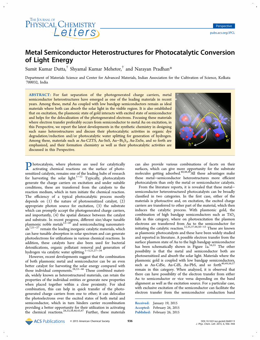
semiconductor heterostructured photocatalysts can be broadlyclassified in two categories. In the first case, either of thematerials is photoactive and, on excitation, the excited chargecarriers are transferred to other part of the material, which theninduces the catalytic process. With plasmonic gold, thecombination of high bandgap semiconductors such as TiO2falls in this category, where on photoexcitation the plasmonelectrons are transferred from Au to the semiconductor forinitiating the catalytic reaction.12,35,37,48,50−53 These are knownas plasmonic photocatalysts and these have been widely studiedand reported in literature. A possible electron transfer from thesurface plasmon state of Au to the high bandgap semiconductorhas been schematically shown in Figure 1a.54,55 The otherpossibility is that the metal and semiconductor both arephotosensitized and absorb the solar light. Materials where theplasmonic gold is coupled with low bandgap semiconductors,such as Au-CdSe, Au-CdS, Au-PbS, and so forth40,49,56,57
remain in this category. When analyzed, it is observed thatthere can have possibility of the electron transfer from eitherAu to semiconductor or vice versa depending on the bandalignment as well as the excitation source. For a particular case,with exclusive excitation of the semiconductor can facilitate theelectron transfer from the semiconductor conduction band
Received: January 19, 2015Accepted: February 26, 2015Published: February 26, 2015
Perspective
pubs.acs.org/JPCL
© 2015 American Chemical Society 936 DOI: 10.1021/acs.jpclett.5b00113J. Phys. Chem. Lett. 2015, 6, 936−944
(CB) to Au electronic level and a schematic presentation ofsuch electronic movement has been shown in Figure 1b.56,58
Similarly, if only Au is excited here, then electron transfer canfollow similar to the scheme shown in Figure 1a, provided thesurface plasmon state remains above the CB of the semi-conductor. But, the case becomes more complicated when bothAu and semiconductors are excited together. Even though mostof the reports predicted the photoexcited electron transfersfrom the excited state of semiconductor to Au, but a recentstudy on Au-CdS showed that, the electron transfer in bothways are possible, though more probable is the transfer fromsemiconductor to metal Au.56 There is also a possibility ofcoupling of the exciton of semiconductor and plasmon of Au.Summarizing all possible processes in this category, we haveshown the carrier transfer protocols in Figure 1c.56,59,60
However, to our understanding, the case where both themetal and semiconductor are photosensitive remains morepromising, as both can absorb solar light and generate a greaternumber of photoexcited charge carriers compared with theother two categories.
However, while considered for metal−semiconductor heter-ostructures, apart from Au, other metals are also been coupledwith various semiconductors and used in photocatalysis. MetalPt remains even more efficient in some cases.28,62 But we focushere mostly the plasmonic metal Au as its surface plasmonresonance (SPR) remains in the intense region of the solarspectrum. Hence, we have confined our discussion mostly toAu-based heterostructures.Apart from the promising photocatalytic properties, these
heterostructured materials also possess interesting chemistry of
their formations, which contributes several new fundamentalaspects in the study of crystal growth in solution.40,43,63
However, in these heterostructures, two different materialshaving different reactivities cannot just be coupled randomly.The lattice mismatch between these materials typically remainshigh, and this became the major hurdle in designing suchheterostructures in solution. Crystallographic orientations ofenergetically favorable facets of both materials are essential tominimize the formation energy and to form the stableheterostructure. Although a large number of such materialsreported are silent over their epitaxial relations, several recentreports suggest that epitaxial binding is possible even if theyhave wide lattice mismatches within their approachedfacets.64,65 Some of the material properties are even retained,irrespective of the nature of the heterojunction, but epitaxialorientations provide stronger bonds, sustainability at highertemperature and also can facilitate efficient carrier trans-portation. Several such materials such as Au-CdSe, Au-ZnSe,Au-CZTS, and so forth have recently been reported in colloidalsolutions having epitaxial connections.6,61,64−66 For our bestunderstanding, the chemistry of formation of these hetero-structures having proper crystallographic orientation providesimportance in architecting the robust nano heterostructures,and this needs to be explored more.Hence, combining the upcoming chemistry of formation of
the nano heterostructures with their photocatalytic properties,in this Perspective, we mostly focus on the very recentdevelopments of heterostructures of Au and low bandgapgreener semiconductors. Emphasis has been given on thecoupled effects of the SPR of Au and exciton of semiconductorin these heterostructures helping in the better transformation ofthe solar energy to the chemical energy. However, we restrictthe discussion to the heterostructured materials developed inthe latest half a decade, their interesting and newly statedformation mechanisms, heteroepitaxies, and their light harvest-ing properties in the implementations of catalysis for organicreactions and light-driven hydrogen evolution from watersplitting.Nano Heterostructures: Some Recent Developments. From theliterature reports, it is revealed that soon after the developmentof high quality quantum confined semiconductor nanostruc-tures, Banin et al.67 developed the fabulous semiconductornanorods with metal tips (Au-CdSe),68 and this became thebreakthrough in developing such heterostructured materials.For more than a decade, enormous efforts have been putforward in designing different new nano heterostructures andu n d e r s t a n d i n g t h e i r s y n t h e t i c c h e m i s -try.28,43,57,62,66,69−74Among these, core/shell structures,75,76
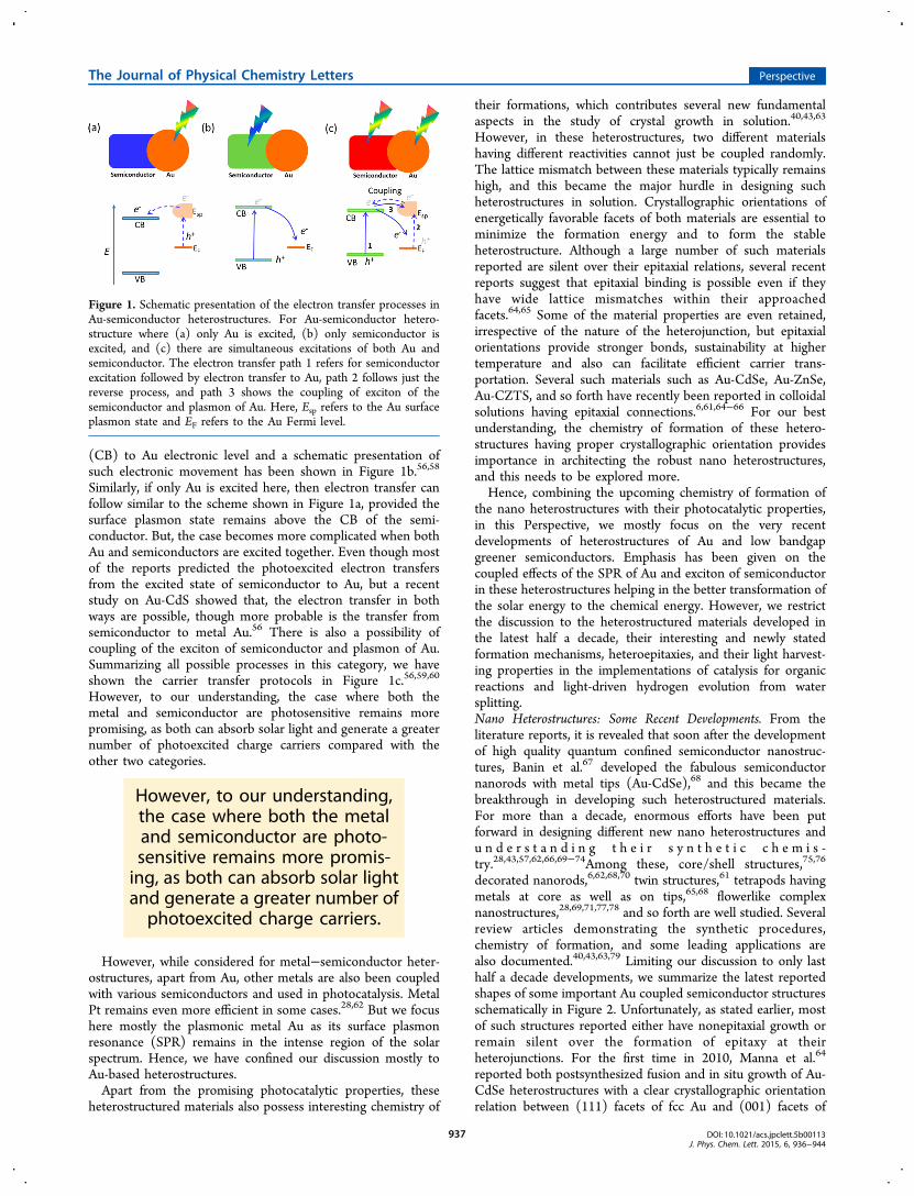
decorated nanorods,6,62,68,70 twin structures,61 tetrapods havingmetals at core as well as on tips,65,68 flowerlike complexnanostructures,28,69,71,77,78 and so forth are well studied. Severalreview articles demonstrating the synthetic procedures,chemistry of formation, and some leading applications arealso documented.40,43,63,79 Limiting our discussion to only lasthalf a decade developments, we summarize the latest reportedshapes of some important Au coupled semiconductor structuresschematically in Figure 2. Unfortunately, as stated earlier, mostof such structures reported either have nonepitaxial growth orremain silent over the formation of epitaxy at theirheterojunctions. For the first time in 2010, Manna et al.64
reported both postsynthesized fusion and in situ growth of Au-CdSe heterostructures with a clear crystallographic orientationrelation between (111) facets of fcc Au and (001) facets of
Figure 1. Schematic presentation of the electron transfer processes inAu-semiconductor heterostructures. For Au-semiconductor hetero-structure where (a) only Au is excited, (b) only semiconductor isexcited, and (c) there are simultaneous excitations of both Au andsemiconductor. The electron transfer path 1 refers for semiconductorexcitation followed by electron transfer to Au, path 2 follows just thereverse process, and path 3 shows the coupling of exciton of thesemiconductor and plasmon of Au. Here, Esp refers to the Au surfaceplasmon state and EF refers to the Au Fermi level.
However, to our understanding,the case where both the metaland semiconductor are photo-sensitive remains more promis-ing, as both can absorb solar lightand generate a greater number ofphotoexcited charge carriers.
The Journal of Physical Chemistry Letters Perspective
DOI: 10.1021/acs.jpclett.5b00113J. Phys. Chem. Lett. 2015, 6, 936−944
937
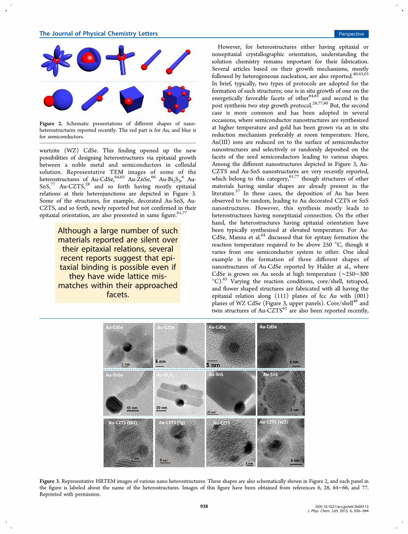
wurtzite (WZ) CdSe. This finding opened up the newpossibilities of designing heterostructures via epitaxial growthbetween a noble metal and semiconductors in colloidalsolution. Representative TEM images of some of theheterostructures of Au-CdSe,64,65 Au-ZnSe,66 Au-Bi2S3,
6 Au-SnS,77 Au-CZTS,28 and so forth having mostly epitaxialrelations at their heterojunctions are depicted in Figure 3.Some of the structures, for example, decorated Au-SnS, Au-CZTS, and so forth, newly reported but not confirmed in theirepitaxial orientation, are also presented in same figure.61,77
However, for heterostructures either having epitaxial ornonepitaxial crystallographic orientation, understanding thesolution chemistry remains important for their fabrication.Several articles based on their growth mechanisms, mostlyfollowed by heterogeneous nucleation, are also reported.40,43,63
In brief, typically, two types of protocols are adopted for theformation of such structures; one is in situ growth of one on theenergetically favorable facets of other64,65 and second is thepost synthesis two step growth protocol.28,77,80 But, the secondcase is more common and has been adopted in severaloccasions, where semiconductor nanostructures are synthesizedat higher temperature and gold has been grown via an in situreduction mechanism preferably at room temperature. Here,Au(III) ions are reduced on to the surface of semiconductornanostructures and selectively or randomly deposited on thefacets of the seed semiconductors leading to various shapes.Among the different nanostructures depicted in Figure 3, Au-CZTS and Au-SnS nanostructures are very recently reported,which belong to this category,61,77 though structures of othermaterials having similar shapes are already present in theliterature.57 In these cases, the deposition of Au has beenobserved to be random, leading to Au decorated CZTS or SnSnanostructures. However, this synthesis mostly leads toheterostructures having nonepitaxial connection. On the otherhand, the heterostructures having epitaxial orientation havebeen typically synthesized at elevated temperature. For Au-CdSe, Manna et al.64 discussed that for epitaxy formation thereaction temperature required to be above 250 °C, though itvaries from one semiconductor system to other. One idealexample is the formation of three different shapes ofnanostructures of Au-CdSe reported by Halder at al., whereCdSe is grown on Au seeds at high temperature (∼250−300°C).65 Varying the reaction conditions, core/shell, tetrapod,and flower shaped structures are fabricated with all having theepitaxial relation along (111) planes of fcc Au with (001)planes of WZ CdSe (Figure 3, upper panels). Core/shell46 andtwin structures of Au-CZTS61 are also been reported recently,
Figure 2. Schematic presentations of different shapes of nano-heterostructures reported recently. The red part is for Au, and blue isfor semiconductors.
Figure 3. Representative HRTEM images of various nano heterostructures. These shapes are also schematically shown in Figure 2, and each panel inthe figure is labeled about the name of the heterostructures. Images of this figure have been obtained from references 6, 28, 64−66, and 77.Reprinted with permission.
Although a large number of suchmaterials reported are silent overtheir epitaxial relations, severalrecent reports suggest that epi-taxial binding is possible even if
they have wide lattice mis-matches within their approached
facets.
The Journal of Physical Chemistry Letters Perspective
DOI: 10.1021/acs.jpclett.5b00113J. Phys. Chem. Lett. 2015, 6, 936−944
938
where the semiconductor CZTS is allowed to grow on Auunder certain reaction condition. Here, the epitaxy has beenobserved with (111) facets of fcc Au with (100) facets of WZCZTS nanostructures. Similarly, ZnSe and Bi2S3 semiconduc-tors are grown on gold seeds at high temperature. Synthesis ofsuch nanostructures needs careful reaction parameter manip-ulation as presence of excess anions can always leads todissolution of Au particles and also possess the chance offorming separate nucleation of semiconductor nanostructures.However, the question arises here regarding the driving forcesfor formation of such epitaxial connection in these hetero-structures in spite of their wide lattice mismatches. Chemistryrelated to this part of heterostructures formation is not yetprecisely explored, and in this Perspective, we emphasized onthe formation of epitaxy at the heterojunctions consideringexamples of several nanoheterostructures.Epitaxial Heterojunction. From the literature reports, it has beenrevealed that when the lattice mismatch remains less than 15%,typically core/shell structures are formed.81 This statementreflects mostly in case of the semiconductor-semiconductorheterostructures. On the other hand, when the lattice mismatchis above 15%, growth is expected on specific sites of the seedcrystal or dislocation of lattice planes may occur at theinterface.66 However, for Au-CdSe, it is reported that
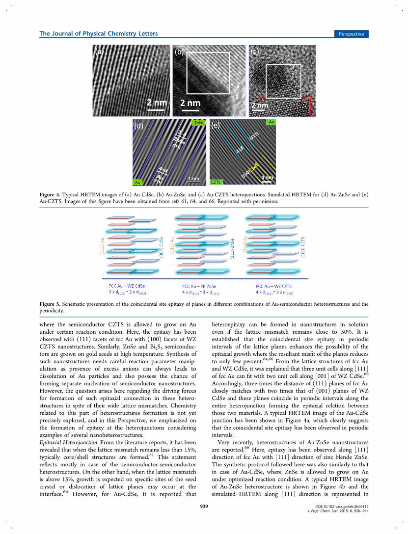
heteroepitaxy can be formed in nanostructures in solutioneven if the lattice mismatch remains close to 50%. It isestablished that the coincidental site epitaxy in periodicintervals of the lattice planes enhances the possibility of theepitaxial growth where the resultant misfit of the planes reducesto only few percent.64,66 From the lattice structures of fcc Auand WZ CdSe, it was explained that three unit cells along [111]of fcc Au can fit with two unit cell along [001] of WZ CdSe.66
Accordingly, three times the distance of (111) planes of fcc Auclosely matches with two times that of (001) planes of WZCdSe and these planes coincide in periodic intervals along theentire heterojunction forming the epitaxial relation betweenthose two materials. A typical HRTEM image of the Au-CdSejunction has been shown in Figure 4a, which clearly suggeststhat the coincidental site epitaxy has been observed in periodicintervals.Very recently, heterostructures of Au-ZnSe nanostructures
are reported.66 Here, epitaxy has been observed along [111]direction of fcc Au with [111] direction of zinc blende ZnSe.The synthetic protocol followed here was also similarly to thatin case of Au-CdSe, where ZnSe is allowed to grow on Auunder optimized reaction condition. A typical HRTEM imageof Au-ZnSe heterostructure is shown in Figure 4b and thesimulated HRTEM along [111] direction is represented in
Figure 4. Typical HRTEM images of (a) Au-CdSe, (b) Au-ZnSe, and (c) Au-CZTS heterojunctions. Simulated HRTEM for (d) Au-ZnSe and (e)Au-CZTS. Images of this figure have been obtained from refs 61, 64, and 66. Reprinted with permission.
Figure 5. Schematic presentation of the coincidental site epitaxy of planes in different combinations of Au-semiconductor heterostructures and theperiodicity.
The Journal of Physical Chemistry Letters Perspective
DOI: 10.1021/acs.jpclett.5b00113J. Phys. Chem. Lett. 2015, 6, 936−944
939
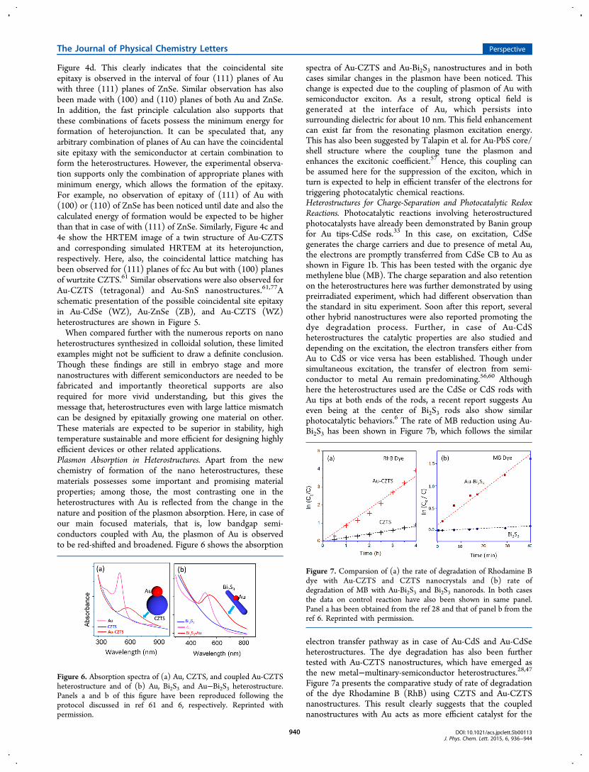
Figure 4d. This clearly indicates that the coincidental siteepitaxy is observed in the interval of four (111) planes of Auwith three (111) planes of ZnSe. Similar observation has alsobeen made with (100) and (110) planes of both Au and ZnSe.In addition, the fast principle calculation also supports thatthese combinations of facets possess the minimum energy forformation of heterojunction. It can be speculated that, anyarbitrary combination of planes of Au can have the coincidentalsite epitaxy with the semiconductor at certain combination toform the heterostructures. However, the experimental observa-tion supports only the combination of appropriate planes withminimum energy, which allows the formation of the epitaxy.For example, no observation of epitaxy of (111) of Au with(100) or (110) of ZnSe has been noticed until date and also thecalculated energy of formation would be expected to be higherthan that in case of with (111) of ZnSe. Similarly, Figure 4c and4e show the HRTEM image of a twin structure of Au-CZTSand corresponding simulated HRTEM at its heterojunction,respectively. Here, also, the coincidental lattice matching hasbeen observed for (111) planes of fcc Au but with (100) planesof wurtzite CZTS.61 Similar observations were also observed forAu-CZTS (tetragonal) and Au-SnS nanostructures.61,77Aschematic presentation of the possible coincidental site epitaxyin Au-CdSe (WZ), Au-ZnSe (ZB), and Au-CZTS (WZ)heterostructures are shown in Figure 5.When compared further with the numerous reports on nano
heterostructures synthesized in colloidal solution, these limitedexamples might not be sufficient to draw a definite conclusion.Though these findings are still in embryo stage and morenanostructures with different semiconductors are needed to befabricated and importantly theoretical supports are alsorequired for more vivid understanding, but this gives themessage that, heterostructures even with large lattice mismatchcan be designed by epitaxially growing one material on other.These materials are expected to be superior in stability, hightemperature sustainable and more efficient for designing highlyefficient devices or other related applications.Plasmon Absorption in Heterostructures. Apart from the newchemistry of formation of the nano heterostructures, thesematerials possesses some important and promising materialproperties; among those, the most contrasting one in theheterostructures with Au is reflected from the change in thenature and position of the plasmon absorption. Here, in case ofour main focused materials, that is, low bandgap semi-conductors coupled with Au, the plasmon of Au is observedto be red-shifted and broadened. Figure 6 shows the absorption
spectra of Au-CZTS and Au-Bi2S3 nanostructures and in bothcases similar changes in the plasmon have been noticed. Thischange is expected due to the coupling of plasmon of Au withsemiconductor exciton. As a result, strong optical field isgenerated at the interface of Au, which persists intosurrounding dielectric for about 10 nm. This field enhancementcan exist far from the resonating plasmon excitation energy.This has also been suggested by Talapin et al. for Au-PbS core/shell structure where the coupling tune the plasmon andenhances the excitonic coefficient.57 Hence, this coupling canbe assumed here for the suppression of the exciton, which inturn is expected to help in efficient transfer of the electrons fortriggering photocatalytic chemical reactions.Heterostructures for Charge-Separation and Photocatalytic RedoxReactions. Photocatalytic reactions involving heterostructuredphotocatalysts have already been demonstrated by Banin groupfor Au tips-CdSe rods.33 In this case, on excitation, CdSegenerates the charge carriers and due to presence of metal Au,the electrons are promptly transferred from CdSe CB to Au asshown in Figure 1b. This has been tested with the organic dyemethylene blue (MB). The charge separation and also retentionon the heterostructures here was further demonstrated by usingpreirradiated experiment, which had different observation thanthe standard in situ experiment. Soon after this report, severalother hybrid nanostructures were also reported promoting thedye degradation process. Further, in case of Au-CdSheterostructures the catalytic properties are also studied anddepending on the excitation, the electron transfers either fromAu to CdS or vice versa has been established. Though undersimultaneous excitation, the transfer of electron from semi-conductor to metal Au remain predominating.56,60 Althoughhere the heterostructures used are the CdSe or CdS rods withAu tips at both ends of the rods, a recent report suggests Aueven being at the center of Bi2S3 rods also show similarphotocatalytic behaviors.6 The rate of MB reduction using Au-Bi2S3 has been shown in Figure 7b, which follows the similar
electron transfer pathway as in case of Au-CdS and Au-CdSeheterostructures. The dye degradation has also been furthertested with Au-CZTS nanostructures, which have emerged asthe new metal−multinary-semiconductor heterostructures.28,47Figure 7a presents the comparative study of rate of degradationof the dye Rhodamine B (RhB) using CZTS and Au-CZTSnanostructures. This result clearly suggests that the couplednanostructures with Au acts as more efficient catalyst for the
Figure 6. Absorption spectra of (a) Au, CZTS, and coupled Au-CZTSheterostructure and of (b) Au, Bi2S3 and Au−Bi2S3 heterostructure.Panels a and b of this figure have been reproduced following theprotocol discussed in ref 61 and 6, respectively. Reprinted withpermission.
Figure 7. Comparsion of (a) the rate of degradation of Rhodamine Bdye with Au-CZTS and CZTS nanocrystals and (b) rate ofdegradation of MB with Au-Bi2S3 and Bi2S3 nanorods. In both casesthe data on control reaction have also been shown in same panel.Panel a has been obtained from the ref 28 and that of panel b from theref 6. Reprinted with permission.
The Journal of Physical Chemistry Letters Perspective
DOI: 10.1021/acs.jpclett.5b00113J. Phys. Chem. Lett. 2015, 6, 936−944
940
photocatalytic reactions compared to only CZTS. In additionto the above materials, recent report on plasmonic Au-SnSheterostructures also show enhancement of the rate of catalyticactivities in the reduction of the dye MB compared to only SnSnanocrystals.77 The mechanism in all these cases follow similarpath, where the charge carriers recombination is suppressedbecause of the coupling of the metal plasmon and semi-conductor exciton, helping its smooth transfer to the organicdye thus enhancing the catalytic reaction rate. This has beenschematically depicted in Figure 1c. For the dye MB, thedecolorization is termed either as degradation or reduction indifferent reports but in either case the electron is transferred toMB, which induces the chemical reaction.Nano Heterostructures for Photocatalytic Water Splitting.Following the similar principle of faster charge carriersseparation in these nano heterostructures, these materials alsohave recently emerged as efficient photo sensitizers for light-driven hydrogen evolution by catalytic water splitting.28,40,46 Inthis process, the energy state of the photoexcited electrons ofthe catalytic materials should be above the redox potential oftransformation of H+ ions to molecular H2.
1 Differentsemiconducting nanostructures having ideal bandgap, havealready been used as photocatalysts for promoting thishydrogen generation process. The efficiency of such systemhas already been shown for different shapes of Au-CZTSnanostructures, an ideal example of metal−multinary-semi-conductor heterostructures.46 The mechanism here is expectedto be similar to that of the photocatalysis for the organicreactions, where the photo generated electron is transferred towater for carrying out the redox reaction of transforming H+ ofwater to H2 gas. Even though this catalytic activity has beenextensively studied for wide variety of semiconductornanostructures, but for nano heterostructures, which are alsoexpected to be efficient materials, they are little explored. Again,among these plasmonic Au coupled with high bandgapsemiconductors where only the Au is excited; the electrontransfer process is somewhat established. On the other hand,for the heterostructures where Au is coupled with low-bandgap,greener semiconductors, where both materials can besimultaneously excited under visible light, the electron transferprocess for carrying out the catalytic activities are yet to beexplored.Typically, for an ideal catalyst, when it is dispersed in water
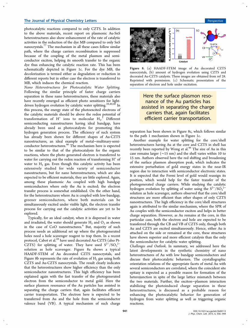
and irradiated, the water should generate H2 and O2 as shownin the case of CoO nanostructures.4 But, majority of suchprocess needs an additional set up where the photogeneratedholes need a hole scavenger reagent to trap them. In a recentprotocol, Cabot et al.28 have used decorated Au-CZTS (also Pt-CZTS) for splitting of water. They have used S2−/SO3
2−
solution as hole scavenger. Figure 8a shows a typicalHAADF-STEM of Au decorated CZTS nanocrystals, andFigure 8b represents the rate of evolution of H2 gas using bothCZTS and Au-CZTS nanocrystals. The result clearly indicatesthat the heterostructures show higher efficiency than the onlysemiconductor nanostructures. This high efficiency has beenexplained again with the fast transfer of the photogeneratedelectron from the semiconductor to metal gold. Here thesurface plasmon resonance of the Au particles has assisted inseparating the charge carriers that, again facilitates efficientcarrier transportation. The electron here is expected to betransferred from Au and the hole from the semiconductorvalence band (VB). A typical mechanism of such charge
separation has been shown in Figure 8c, which follows similarto the path 1 mechanism shown in Figure 1c.Another example for water splitting for the core/shell
heterostructures having Au at the core and CZTS in shell hasrecently been reported by Wong et al.46 The size of Au in thiscase remains larger (∼15 nm) and the shell varies within 10 to15 nm. Authors observed here the red shifting and broadeningof the surface plasmon absorption peak, which indicates theextensive perturbation of gold energy states in the near-IRregion due to interaction with semiconductor electronic states.It is expected that the Fermi level of gold would reassign itsposition, which would help for the faster transfer of thephotogenerated charge carriers. While studying the catalytichydrogen evolution by splitting of water using the S2−/SO3
2−
solution as hole scavenger, authors observed that the core/shellstructures are more efficient than other shapes of only CZTSnanostructures. The high efficiency in the core/shell structuresagain is attributed to the similar mechanism, where the SPR ofAu couples with the semiconductor exciton and helps in bettercharge separation. However, as Au remains at the core, in thisparticular case, both the electron and hole are expected to betransferred through the CB and VB of CZTS only, though bothAu and CZTS are excited simultaneously. Hence, either Au isattached on the side or remained at the core, these structureshave shown superior and more efficient catalysis than the onlythe semiconductor for catalytic water splitting.Challenges and Outlook. In summary, we addressed here thelatest developments in the synthetic chemistry of nanoheterostructures of Au with low bandgap semiconductors anddiscuss their photocatalytic behaviors. The crystallographicorientation relations of the appropriate facets of metal Au withseveral semiconductors are correlated, where the coincident siteepitaxy is expected as a possible reason for formation of theheterojunction in spite of the large lattice mismatch betweenthe two materials. Further, the exciton−plasmon interactionstabilizing the photoinduced charge separation in theseheterostructures, is discussed as a probable reason forenhancing the photocatalytic behavior for generation ofhydrogen from water splitting as well as triggering organicreactions.
Figure 8. (a) HAADF-STEM image of Au decorated CZTSnanocrystals, (b) amount of hydrogen evolution using CZTS anddecorated Au-CZTS catalysts. These images are obtained from ref 28.Reprinted with permission. (c) Schematic presentation of theseparation of electron and hole under excitation.
Here the surface plasmon reso-nance of the Au particles has
assisted in separating the chargecarriers that, again facilitatesefficient carrier transportation.
The Journal of Physical Chemistry Letters Perspective
DOI: 10.1021/acs.jpclett.5b00113J. Phys. Chem. Lett. 2015, 6, 936−944
941
However, only a few such materials are developed till date,but their promising photocatalytic activities encourage develop-ment of a wide variety of such materials, where the appropriateband alignment would support more facile electron transfer.Though analyzed, on the one hand, the chemistry ofarchitecting of these heterostructures needs to be properlyunderstood. The heterogeneous nucleation formation either forthe growth of semiconductor on metal or vice versa needs to beoptimized without allowing formation of new nucleations. Next,the shape of the nanostructures also plays a crucial role indetermining the efficiency of the catalysis. For example, whencompared with core/shell Au/TiO2nanostructures, Janus-typeheterostructures show superior catalytic behavior for thesplitting of water and generation of hydrogen.55 On thecontrary, a recent report has shown that for core/shell Au/CZTS, the rate of hydrogenation evolution from water is morethan the Au-CZTS Janus-type structure.28 All these resultsindeed suggest that the shape of the nanostructure andparticularly the position of Au are critical in determining theelectron transfer process and the rate of the catalytic activities.Hence, wide variety of nanostructures with different shapesneeds to be designed and details of the catalytic activities are tobe further studied for understanding a clear and concretemechanism. Next, as the metallic nature of the Au and itsplasmon help with the separation of the photogenerated chargecarriers, it is important to study the catalytic activities byvarying the size of Au particles. It is widely known that whenthe dimension of Au falls below certain nanometers, themetallic character reduces and it behaves more like semi-conductor and the plasmonic behavior of Au reduces. Usingboth plasmonic and nonplasmonic Au particles, it is observedrecently for their heterostructures with SnS that, the catalyticactivities drastically reduce with reduction of plasmonicbehavior.77 Although Au is also known for quenching thequantum dot exciton emission, a recent report also suggeststhat for cluster size nonplasmonic Au, the CdSe still retains theemission to significant extent.82 These results suggest that thesize of Au also plays a crucial role in determining the electrontransfer ability and also the catalytic behaviors. Hence, adetailed study in this respect is warranted, and also, moresemiconductor heterostructures with different sizes of Au needto be investigated to come out with a conclusion. In addition,the coupling of surface plasmon of Au and the semiconductorexciton, which helps in the delocalization of the electrons intheir excited states and enhancing the catalytic activities, canalso be tuned more efficiently. Once this plasmon−excitoncoupling is properly understood, the catalytic activities can becontrolled and these materials can be implemented forcatalyzing a wide variety of organic reactions.Apart from the chemistry of formation and size and shape
variation in the semiconductor as well as Au, the mostimportant part is studying the photophysics to understand theinvolved electron transfer processes. These studies have beenlimited to CdS, CdSe, and few widely studied materials.However, this needs deep investigation with study of ultrafastspectroscopy in various heterostructure systems for obtaining ageneric conclusion. The particular system discussed in thisPerspective, where the metal and semiconductor both areexcited, the electron transfer processes indeed remainsunsolved and complicated. The movement of electrons andholes and their involvement for the catalysis need to be deeplyinvestigated, and hence, a detailed study of the photophysics,including single-particle spectroscopy analysis, is warranted.
Finally, the photocatalysis needs to be further studied with awide variety of organic systems, including degradation ofpollutants and common laboratory organic reactions. This canbe extended to biochemical reactions and also as efficientprocess for detoxifying selective bioorganisms. Importantly, theheterostructures are expected as ideal photoresponse materialsfor efficient solar light harvesting and also for implementationsin photovoltaics.
■ AUTHOR INFORMATIONCorresponding Author*E-mail: [email protected].
Author Contributions†S.K.D. and S.K.M. have equal contributions.
NotesThe authors declare no competing financial interest.Biographies
Sumit Kumar Dutta received his B.Sc. from St. Xavier’s College,Kolkata (2012), and M.Sc. from IIT Bombay, India (2014). He is aSPM fellow and currently is doing his Doctoral study under Dr.Narayan Pradhan at “Indian Association for the Cultivation of Science”Jadavpur, Kolkata, India.
Shyamal Kumar Mehetor received his B.Sc. from Burdwan University(2012) and M.Sc. from IIT Kharagpur, India (2014). He is currentlydoing his Doctoral study under Dr. Narayan Pradhan at “IndianAssociation for the Cultivation of Science” Jadavpur, Kolkata, India.
Narayan Pradhan is graduated from IIT Kharagpur, India (2001) andcurrently working as an Associate Professor in the Department ofMaterials Science and also as an associate of the Centre for AdvancedMaterials, “Indian Association for the Cultivation of Science” Jadavpur,Kolkata, India. His major research interests are the synthesis, surfacefictionalization, and photophysical properties of colloidal semi-conductor and transition metal-doped semiconductor nanomaterials.See http://www.iacs.res.in/matsc/msnp/ for further details.
■ ACKNOWLEDGMENTSDST of India is acknowledged for funding (DST/SJF/CSA-01/2010-2011). N.P. acknowledge to DST Swarnajayanti Project,and S.K.M. and S.K.D. to CSIR, India for fellowships.
■ REFERENCES(1) Maeda, K.; Domen, K. Photocatalytic Water Splitting: RecentProgress and Future Challenges. J. Phys. Chem. Lett. 2010, 1, 2655−2661.(2) Zhao, J.; Osterloh, F. E. Photochemical Charge Separation inNanocrystal Photocatalyst Films: Insights from Surface PhotovoltageSpectroscopy. J. Phys. Chem. Lett. 2014, 5, 782−786.(3) Osterloh, F. E. Boosting the Efficiency of Suspended Photo-catalysts for Overall Water Splitting. J. Phys. Chem. Lett. 2014, 5,2510−2511.(4) Liao, L.; Zhang, Q.; Su, Z.; Zhao, Z.; Wang, Y.; Li, Y.; Lu, X.;Wei, D.; Feng, G.; Yu, Q.; et al. Efficient Solar Water-Splitting Using aNanocrystalline CoO Photocatalyst. Nat. Nanotechnol. 2014, 9, 69−73.(5) Ida, S.; Ishihara, T. Recent Progress in Two-Dimensional OxidePhotocatalysts for Water Splitting. J. Phys. Chem. Lett. 2014, 5, 2533−2542.(6) Manna, G.; Bose, R.; Pradhan, N. Photocatalytic Au-Bi2S3Heteronanostructures. Angew. Chem., Int. Ed. 2014, 53, 6743−6746.(7) Eley, C.; Li, T.; Liao, F.; Fairclough, S. M.; Smith, J. M.; Smith,G.; Tsang, S. C. E. Nanojunction-Mediated Photocatalytic Enhance-ment in Heterostructured CdS/ZnO, CdSe/ZnO, and CdTe/ZnONanocrystals. Angew. Chem., Int. Ed. 2014, 53, 7838−7842.
The Journal of Physical Chemistry Letters Perspective
DOI: 10.1021/acs.jpclett.5b00113J. Phys. Chem. Lett. 2015, 6, 936−944
942

(8) Park, Y.; Kim, W.; Monllor-Satoca, D.; Tachikawa, T.; Majima,T.; Choi, W. Role of Interparticle Charge Transfers in AgglomeratedPhotocatalyst Nanoparticles: Demonstration in Aqueous Suspensionof Dye-Sensitized TiO2. J. Phys. Chem. Lett. 2013, 4, 189−194.(9) Khon, E.; Lambright, K.; Khnayzer, R. S.; Moroz, P.; Perera, D.;Butaeva, E.; Lambright, S.; Castellano, F. N.; Zamkov, M. Improvingthe Catalytic Activity of Semiconductor Nanocrystals throughSelective Domain Etching. Nano Lett. 2013, 13, 2016−2023.(10) Kamat, P. V. Manipulation of Charge Transfer AcrossSemiconductor Interface. A Criterion That Cannot Be Ignored inPhotocatalyst Design. J. Phys. Chem. Lett. 2012, 3, 663−672.(11) Miseki, Y.; Kusama, H.; Sugihara, H.; Sayama, K. Cs-ModifiedWO3 Photocatalyst Showing Efficient Solar Energy Conversion for O2
Production and Fe(III) Ion Reduction under Visible Light. J. Phys.Chem. Lett. 2010, 1, 1196−1200.(12) Linic, S.; Christopher, P.; Ingram, D. B. Plasmonic-MetalNanostructures for Efficient Conversion of Solar to Chemical Energy.Nat. Mater. 2011, 10, 911−921.(13) Duan, C.; Wang, H.; Ou, X.; Li, F.; Zhang, X. Efficient VisibleLight Photocatalyst Fabricated by Depositing Plasmonic Ag Nano-particles on Conductive Polymer-Protected Si Nanowire Arrays forPhotoelectrochemical Hydrogen Generation. ACS Appl. Mater.Interfaces 2014, 6, 9742−9750.(14) Pradhan, N.; Pal, A.; Pal, T. Catalytic Reduction of AromaticNitro Compounds by Coinage Metal Nanoparticles. Langmuir 2001,17, 1800−1802.(15) Pradhan, N.; Pal, A.; Pal, T. Silver Nanoparticle CatalyzedReduction of Aromatic Nitro Compounds. Colloids Surf., A 2002, 196,247−257.(16) Zheng, Z.; Tachikawa, T.; Majima, T. Single-Particle Study ofPt-Modified Au Nanorods for Plasmon-Enhanced Hydrogen Gen-eration in Visible to Near-Infrared Region. J. Am. Chem. Soc. 2014,136, 6870−6873.(17) Lou, Z.; Wang, Z.; Huang, B.; Dai, Y. Synthesis and Activity ofPlasmonic Photocatalysts. ChemCatChem. 2014, 6, 2456−2476.(18) Zhang, L.; Kim, H. Y.; Henkelman, G. CO Oxidation at the Au−Cu Interface of Bimetallic Nanoclusters Supported on CeO2(111). J.Phys. Chem. Lett. 2013, 4, 2943−2947.(19) Zhang, J.; Alexandrova, A. N. The Golden Crown: A Single AuAtom that Boosts the CO Oxidation Catalyzed by a Palladium Clusteron Titania Surfaces. J. Phys. Chem. Lett. 2013, 4, 2250−2255.(20) Xing, Y.; Cai, Y.; Vukmirovic, M. B.; Zhou, W.-P.; Karan, H.;Wang, J. X.; Adzic, R. R. Enhancing Oxygen Reduction ReactionActivity via Pd-Au Alloy Sublayer Mediation of Pt MonolayerElectrocatalysts. J. Phys. Chem. Lett. 2010, 1, 3238−3242.(21) Trotochaud, L.; Mills, T. J.; Boettcher, S. W. An OptocatalyticModel for Semiconductor-Catalyst Water-Splitting PhotoelectrodesBased on In Situ Optical Measurements on Operational Catalysts. J.Phys. Chem. Lett. 2013, 4, 931−935.(22) Ma, S. S. K.; Hisatomi, T.; Maeda, K.; Moriya, Y.; Domen, K.Enhanced Water Oxidation on Ta3N5 Photocatalysts by Modificationwith Alkaline Metal Salts. J. Am. Chem. Soc. 2012, 134, 19993−19996.(23) Maeda, K. Z-Scheme Water Splitting Using Two DifferentSemiconductor Photocatalysts. ACS Catal. 2013, 3, 1486−1503.(24) Martin, D. J.; Qiu, K.; Shevlin, S. A.; Handoko, A. D.; Chen, X.;Guo, Z.; Tang, J. Highly Efficient Photocatalytic H2 Evolution fromWater using Visible Light and Structure-Controlled Graphitic CarbonNitride. Angew. Chem., Int. Ed. 2014, 53, 9240−9245.(25) Kim, J.-H.; Kim, J.-H. Encapsulated Triplet-Triplet Annihilation-Based Upconversion in the Aqueous Phase for Sub-Band-GapSemiconductor Photocatalysis. J. Am. Chem. Soc. 2012, 134, 17478−17481.(26) Li, Q.; Guo, B.; Yu, J.; Ran, J.; Zhang, B.; Yan, H.; Gong, J. R.Highly Efficient Visible-Light-Driven Photocatalytic Hydrogen Pro-duction of CdS-Cluster-Decorated Graphene Nanosheets. J. Am.Chem. Soc. 2011, 133, 10878−10884.(27) Zandi, O.; Hamann, T. W. Enhanced Water Splitting EfficiencyThrough Selective Surface State Removal. J. Phys. Chem. Lett. 2014, 5,1522−1526.
(28) Yu, X.; Shavel, A.; An, X.; Luo, Z.; Ibanez, M.; Cabot, A.Cu2ZnSnS4-Pt and Cu2ZnSnS4-Au Heterostructured Nanoparticles forPhotocatalytic Water Splitting and Pollutant Degradation. J. Am. Chem.Soc. 2014, 136, 9236−9239.(29) Dotan, H.; Mathews, N.; Hisatomi, T.; Gratzel, M.; Rothschild,A. On the Solar to Hydrogen Conversion Efficiency of Photo-electrodes for Water Splitting. J. Phys. Chem. Lett. 2014, 5, 3330−3334.(30) Zhang, M.; Lin, Y.; Mullen, T. J.; Lin, W.-f.; Sun, L.-D.; Yan, C.-H.; Patten, T. E.; Wang, D.; Liu, G.-y. Improving Hematite’s SolarWater Splitting Efficiency by Incorporating Rare-Earth UpconversionNanomaterials. J. Phys. Chem. Lett. 2012, 3, 3188−3192.(31) Noji, T.; Suzuki, H.; Gotoh, T.; Iwai, M.; Ikeuchi, M.; Tomo, T.;Noguchi, T. Photosystem II-Gold Nanoparticle Conjugate as aNanodevice for the Development of Artificial Light-Driven Water-Splitting Systems. J. Phys. Chem. Lett. 2011, 2, 2448−2452.(32) Zhong, D. K.; Sun, J.; Inumaru, H.; Gamelin, D. R. Solar WaterOxidation by Composite Catalyst/α-Fe2O3 Photoanodes. J. Am. Chem.Soc. 2009, 131, 6086−6087.(33) Costi, R.; Saunders, A. E.; Elmalem, E.; Salant, A.; Banin, U.Visible Light-Induced Charge Retention and Photocatalysis withHybrid CdSe-Au Nanodumbbells. Nano Lett. 2008, 8, 637−641.(34) Ingram, D. B.; Linic, S. Water Splitting on CompositePlasmonic-Metal/Semiconductor Photoelectrodes: Evidence for Se-lective Plasmon-Induced Formation of Charge Carriers Near theSemiconductor Surface. J. Am. Chem. Soc. 2011, 133, 5202−5205.(35) DuChene, J. S.; Sweeny, B. C.; Johnston-Peck, A. C.; Su, D.;Stach, E. A.; Wei, W. D. Prolonged Hot Electron Dynamics inPlasmonic-Metal/Semiconductor Heterostructures with Implicationsfor Solar Photocatalysis. Angew. Chem., Int. Ed. 2014, 53, 7887−7891.(36) Naya, S.-i.; Niwa, T.; Kume, T.; Tada, H. Visible-Light-InducedElectron Transport from Small to Large Nanoparticles in BimodalGold Nanoparticle-Loaded Titanium(IV) Oxide. Angew. Chem., Int. Ed.2014, 53, 7305−7309.(37) Wang, F.; Jiang, Y.; Gautam, A.; Li, Y.; Amal, R. Exploring theOrigin of Enhanced Activity and Reaction Pathway for PhotocatalyticH2 Production on Au/B-TiO2 Catalysts. ACS Catal. 2014, 4, 1451−1457.(38) Jakob, M.; Levanon, H.; Kamat, P. V. Charge Distributionbetween UV-Irradiated TiO2 and Gold Nanoparticles: Determinationof Shift in the Fermi Level. Nano Lett. 2003, 3, 353−358.(39) Li, J.; Cushing, S. K.; Zheng, P.; Senty, T.; Meng, F.; Bristow, A.D.; Manivannan, A.; Wu, N. Solar Hydrogen Generation by a CdS-Au-TiO2 Sandwich Nanorod Array Enhanced with Au Nanoparticle asElectron Relay and Plasmonic Photosensitizer. J. Am. Chem. Soc. 2014,136, 8438−8449.(40) Costi, R.; Saunders, A. E.; Banin, U. Colloidal HybridNanostructures: A New Type of Functional Materials. Angew. Chem.,Int. Ed. 2010, 49, 4878−4897.(41) Elias, W. C.; Eising, R.; Silva, T. R.; Albuquerque, B. L.;Martendal, E.; Meier, L.; Domingos, J. B. Screening the Formation ofSilver Nanoparticles Using a New Reaction Kinetics MultivariateAnalysis and Assessing Their Catalytic Activity in the Reduction ofNitroaromatic Compounds. J. Phys. Chem. C 2014, 118, 12962−12971.(42) Subramanian, V.; Wolf, E.; Kamat, P. V. Semiconductor−MetalComposite Nanostructures. To What Extent Do Metal NanoparticlesImprove the Photocatalytic Activity of TiO2 Films? J. Phys. Chem. B2001, 105, 11439−11446.(43) Uri, B.; Yuval, B.-S.; Kathy, V. Hybrid Semiconductor−MetalNanoparticles: From Architecture to Function. Chem. Mater. 2014, 26,97−110.(44) Vidal, A. B.; Feria, L.; Evans, J.; Takahashi, Y.; Liu, P.;Nakamura, K.; Illas, F.; Rodriguez, J. A. CO2 Activation and MethanolSynthesis on Novel Au/TiC and Cu/TiC Catalysts. J. Phys. Chem. lett.2012, 3, 2275−2280.(45) Kim, H. Y.; Henkelman, G. CO Oxidation at the Interface of AuNanoclusters and the Stepped-CeO2(111) Surface by the Mars−vanKrevelen Mechanism. J. Phys. Chem. Lett. 2013, 4, 216−221.(46) Ha, E.; Lee, L. Y. S.; Wang, J.; Li, F.; Wong, K.-Y.; Tsang, S. C.E. Significant Enhancement in Photocatalytic Reduction of Water to
The Journal of Physical Chemistry Letters Perspective
DOI: 10.1021/acs.jpclett.5b00113J. Phys. Chem. Lett. 2015, 6, 936−944
943

Hydrogen by Au/Cu2ZnSnS4 Nanostructure. Adv. Mater. 2014, 26,3496−3500.(47) Dilsaver, P. S.; Reichert, M. D.; Hallmark, B. L.; Thompson, M.J.; Vela, J. Cu2ZnSnS4-Au Heterostructures: Toward GreenerChalcogenide-Based Photocatalysts. J. Phys. Chem. C 2014, 118,21226−21234.(48) Xing, M.-Y.; Yang, B.-X.; Yu, H.; Tian, B.-Z.; Bagwasi, S.; Zhang,J.-L.; Gong, X.-Q. Enhanced Photocatalysis by Au NanoparticleLoading on TiO2 Single-Crystal(001) and(110) Facets. J. Phys. Chem.Lett. 2013, 4, 3910−3917.(49) Sheldon, M. T.; Trudeau, P. E.; Mokari, T.; Wang, L. W.;Alivisatos, A. P. Enhanced Semiconductor Nanocrystal Conductancevia Solution Grown Contacts. Nano Lett. 2009, 9, 3676−3682.(50) Bian, Z.; Tachikawa, T.; Zhang, P.; Fujitsuka, M.; Majima, T.Au/TiO2 Superstructure-Based Plasmonic Photocatalysts ExhibitingEfficient Charge Separation and Unprecedented Activity. J. Am. Chem.Soc. 2014, 136, 458−465.(51) Farnesi Camellone, M.; Marx, D. On the Impact of Solvation ona Au/TiO2 Nanocatalyst in Contact with Water. J. Phys. Chem. Lett.2013, 4, 514−518.(52) Subramanian, V.; Wolf, E. E.; Kamat, P. V. Catalysis with TiO2/Gold Nanocomposites. Effect of Metal Particle Size on the FermiLevel Equilibration. J. Am. Chem. Soc. 2004, 126, 4943−4950.(53) Cozzoli, P. D.; Curri, M. L.; Giannini, C.; Agostiano, A.Synthesis of TiO2-Au Composites by Titania-Nanorod-AssistedGeneration of Gold Nanoparticles at Aqueous/Nonpolar Interfaces.Small 2006, 2, 413−421.(54) Furube, A.; Du, L.; Hara, K.; Katoh, R.; Tachiya, M. UltrafastPlasmon-Induced Electron Transfer from Gold Nanodots into TiO2
Nanoparticles. J. Am. Chem. Soc. 2007, 129, 14852−14853.(55) Seh Zhi, W.; Liu, S.; Low, M.; Zhang, S.-Y.; Liu, Z.; Mlayah, A.;Han, M.-Y. Janus Au-TiO2 Photocatalysts with Strong Localization ofPlasmonic Near-Fields for Efficient Visible-Light Hydrogen Gener-ation. Adv. Mater. 2012, 24, 2310−2314.(56) Ha, J. W.; Ruberu, T. P. A.; Han, R.; Dong, B.; Vela, J.; Fang, N.Super-Resolution Mapping of Photogenerated Electron and HoleSeparation in Single Metal−Semiconductor Nanocatalysts. J. Am.Chem. Soc. 2014, 136, 1398−1408.(57) Lee, J.-S.; Shevchenko, E. V.; Talapin, D. V. Au-PbS Core−ShellNanocrystals Plasmonic Absorption Enhancement and ElectricalDoping via Intra-particle Charge Transfer. J. Am. Chem. Soc. 2008,130, 9673−9675.(58) Chen, W.-T.; Yang, T.-T.; Hsu, Y.-J. Au-CdS Core−ShellNanocrystals with Controllable Shell Thickness and PhotoinducedCharge Separation Property. Chem. Mater. 2008, 20, 7204−7206.(59) Zhang, J.; Tang, Y.; Lee, K.; Ouyang, M. Tailoring Light−Matter−Spin Interactions in Colloidal Hetero-Nanostructures. Nature2010, 466, 91−95.(60) Wu, K.; Rodriguez-Cordoba, W. E.; Yang, Y.; Lian, T. Plasmon-Induced Hot Electron Transfer from the Au Tip to CdS Rod in CdS-Au Nanoheterostructures. Nano Lett. 2013, 13, 5255−5263.(61) Patra, B. K.; Shit, A.; Guria, A. K.; Sarkar, S.; Prusty, G.;Pradhan, N. Coincident Site Epitaxy at the Junction of Au-Cu2ZnSnS4Hetero-Nanostructures. Chem. Mater. 2015, 27, 650−657.(62) Amirav, L.; Alivisatos, A. P. Photocatalytic HydrogenProduction with Tunable Nanorod Heterostructures. J. Phys. Chem.Lett. 2010, 1, 1051−1054.(63) Cozzoli, P. D.; Pellegrino, T.; Manna, L. Synthesis, Propertiesand Perspectives of Hybrid Nanocrystal Structures. Chem. Soc. Rev.2006, 35, 1195−1208.(64) Figuerola, A.; van Huis, M.; Zanella, M.; Genovese, A.; Marras,S.; Falqui, A.; Zandbergen, H. W.; Cingolani, R.; Manna, L. EpitaxialCdSe-Au Nanocrystal Heterostructures by Thermal Annealing. NanoLett. 2010, 10, 3028−3036.(65) Haldar, K. K.; Pradhan, N.; Patra, A. Formation ofHeteroepitaxy in Different Shapes of Au-CdSe Metal-SemiconductorHybrid Nanostructures. Small 2013, 9, 3424−3432.(66) Bose, R.; Abdul Wasey, A. H. M.; Das, G. P.; Pradhan, N.Heteroepitaxial Junction in Au-ZnSe Nanostructure: Experiment
versus First-Principle Simulation. J. Phys. Chem. Lett. 2014, 5, 1892−1898.(67) Murray, C. B.; Norris, D. J.; Bawendi, M. G. Synthesis andCharacterization of Nearly Monodisperse CdE (E = Sulfur, Selenium,Tellurium) Semiconductor Nanocrystallites. J. Am. Chem. Soc. 1993,115, 8706−8715.(68) Mokari, T.; Rothenberg, E.; Popov, I.; Costi, R.; Banin, U.Selective Growth of Metal Tips onto Semiconductor Quantum Rodsand Tetrapods. Science 2004, 304, 1787−1790.(69) Li, X.; Lian, J.; Lin, M.; Chan, Y. Light-Induced SelectiveDeposition of Metals on Gold-Tipped CdSe-Seeded CdS Nanorods. J.Am. Chem. Soc. 2010, 133, 672−675.(70) Chakrabortty, S.; Xing, G.; Xu, Y.; Ngiam, S. W.; Mishra, N.;Sum, T. C.; Chan, Y. Engineering Fluorescence in Au-Tipped, CdSe-Seeded CdS Nanoheterostructures. Small 2011, 7, 2847−52.(71) Mishra, N.; Lian, J.; Chakrabortty, S.; Lin, M.; Chan, Y. UnusualSelectivity of Metal Deposition on Tapered Semiconductor Nano-structures. Chem. Mater. 2012, 24, 2040−2046.(72) Chakrabortty, S.; Yang, J. A.; Tan, Y. M.; Mishra, N.; Chan, Y.Asymmetric Dumbbells from Selective Deposition of Metals onSeeded Semiconductor Nanorods. Angew. Chem., Int. Ed. 2010, 49,2888−2892.(73) Pellegrino, T.; Fiore, A.; Carlino, E.; Giannini, C.; Cozzoli, P.D.; Ciccarella, G.; Respaud, M.; Palmirotta, L.; Cingolani, R.; Manna,L. Heterodimers Based on CoPt3-Au Nanocrystals with TunableDomain Size. J. Am. Chem. Soc. 2006, 128, 6690−6698.(74) Pacholski, C.; Kornowski, A.; Weller, H. Nanomaterials: Site-Specific Photodeposition of Silver on ZnO Nanorods. Angew. Chem.,Int. Ed. 2004, 43, 4774−4777.(75) Sun, Z.; Yang, Z.; Zhou, J.; Yeung, M. H.; Ni, W.; Wu, H.;Wang, J. A General Approach to the Synthesis of Gold-Metal SulfideCore−Shell and Heterostructures. Angew. Chem., Int. Ed. 2009, 48,2881−2885.(76) Lee, J.-S.; Shevchenko, E. V.; Talapin, D. V. Au−PbS Core−Shell Nanocrystals: Plasmonic Absorption Enhancement and ElectricalDoping via Intra-Particle Charge Transfer. J. Am. Chem. Soc. 2008,130, 9673−9675.(77) Patra, B. K.; Guria, A. K.; Dutta, A.; Shit, A.; Pradhan, N. Au-SnS Hetero Nanostructures: Size of Au Matters. Chem. Mater. 2014,26, 7194−7200.(78) Buonsanti, R.; Grillo, V.; Carlino, E.; Giannini, C.; Curri, M. L.;Innocenti, C.; Sangregorio, C.; Achterhold, K.; Parak, F. G.; Agostiano,A.; et al. Seeded Growth of Asymmetric Binary Nanocrystals Made ofa Semiconductor TiO2 Rodlike Section and a Magnetic γ-Fe2O3Spherical Domain. J. Am. Chem. Soc. 2006, 128, 16953−16970.(79) Nag, A.; Kundu, J.; Hazarika, A. Seeded-Growth, Nanocrystal-Fusion, Ion-Exchange and Inorganic-Ligand Mediated Formation ofSemiconductor-Based Colloidal Heterostructured Nanocrystals. Crys-tEngComm 2014, 16, 9391−9407.(80) Mokari, T.; Sztrum, C. G.; Salant, A.; Rabani, E.; Banin, U.Formation of Asymmetric One-Sided Metal-Tipped SemiconductorNanocrystal Dots and Rods. Nat. Mater. 2005, 4, 855−863.(81) Reiss, P.; Protiere, M.; Li, L. Core/Shell SemiconductorNanocrystals. Small 2009, 5, 154−168.(82) Soni, U.; Tripathy, P.; Sapra, S. Photocatalysis fromFluorescence-Quenched CdSe/Au Nanoheterostructures: A Size-Dependent Study. J. Phys. Chem. Lett. 2014, 5, 1909−1916.
The Journal of Physical Chemistry Letters Perspective
DOI: 10.1021/acs.jpclett.5b00113J. Phys. Chem. Lett. 2015, 6, 936−944
944
Related Documents