MOSFET Metal Oxide Semiconductor Field Effect Transistors EBB424E Dr. Sabar D. Hutagalung School of Materials & Mineral Resources Engineering, Universiti Sains Malaysia

Welcome message from author
This document is posted to help you gain knowledge. Please leave a comment to let me know what you think about it! Share it to your friends and learn new things together.
Transcript
MOSFETMetal Oxide Semiconductor Field Effect Transistors
EBB424E
Dr. Sabar D. HutagalungSchool of Materials & Mineral Resources Engineering, Universiti Sains Malaysia

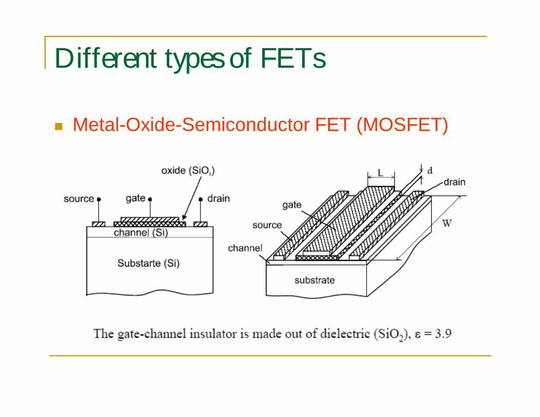
Different types of FETs
Junction FET (JFET) Metal-Oxide-Semiconductor FET (MOSFET) Metal-Semiconductor FET (MESFET)

Different types of FETs
Junction FET (JFET)
Different types of FETs
Metal-Oxide-Semiconductor FET (MOSFET)
Different types of FETs
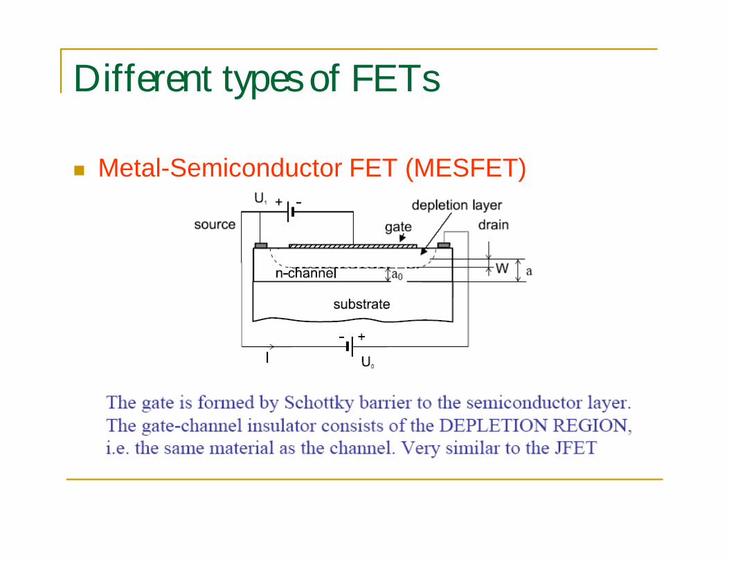
Metal-Semiconductor FET (MESFET)
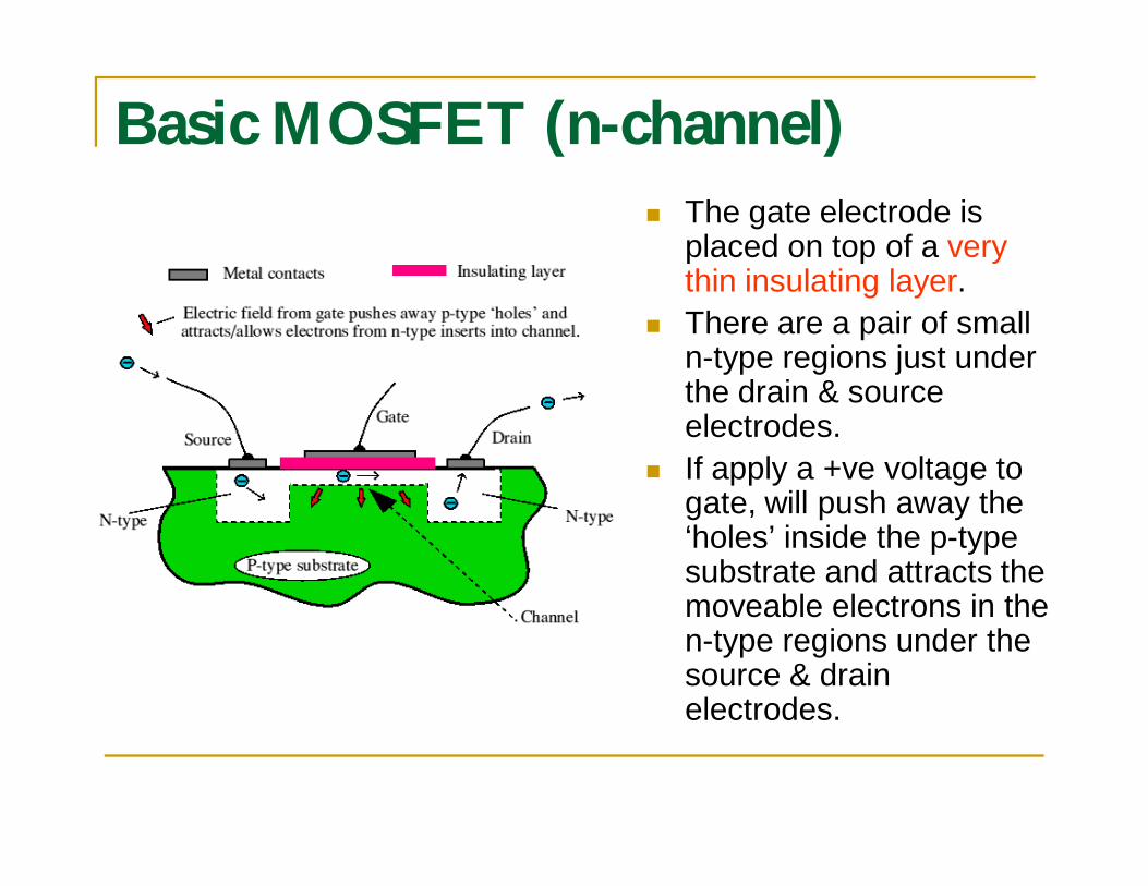
Basic MOSFET (n-channel) The gate electrode is
placed on top of a very thin insulating layer.
There are a pair of small n-type regions just under the drain & source electrodes.
If apply a +ve voltage to gate, will push away the ‘holes’ inside the p-type substrate and attracts the moveable electrons in the n-type regions under the source & drain electrodes.
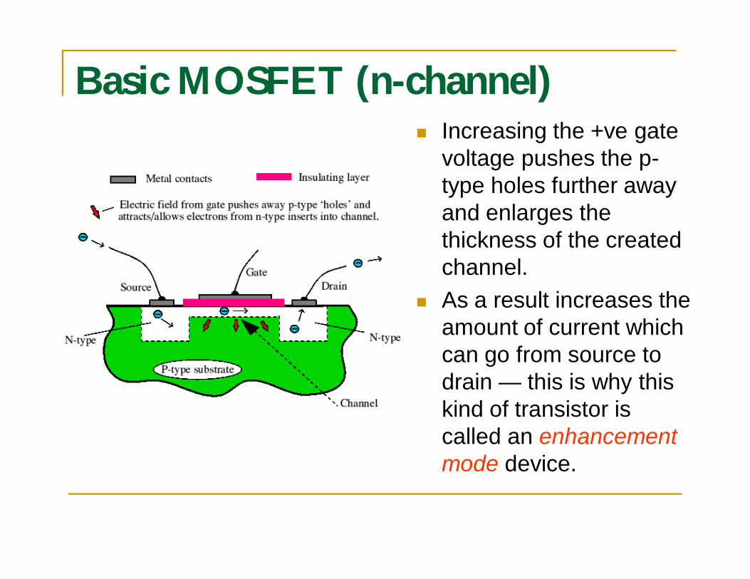
Basic MOSFET (n-channel) Increasing the +ve gate
voltage pushes the p-type holes further away and enlarges the thickness of the created channel.
As a result increases the amount of current which can go from source to drain — this is why this kind of transistor is called an enhancement mode device.
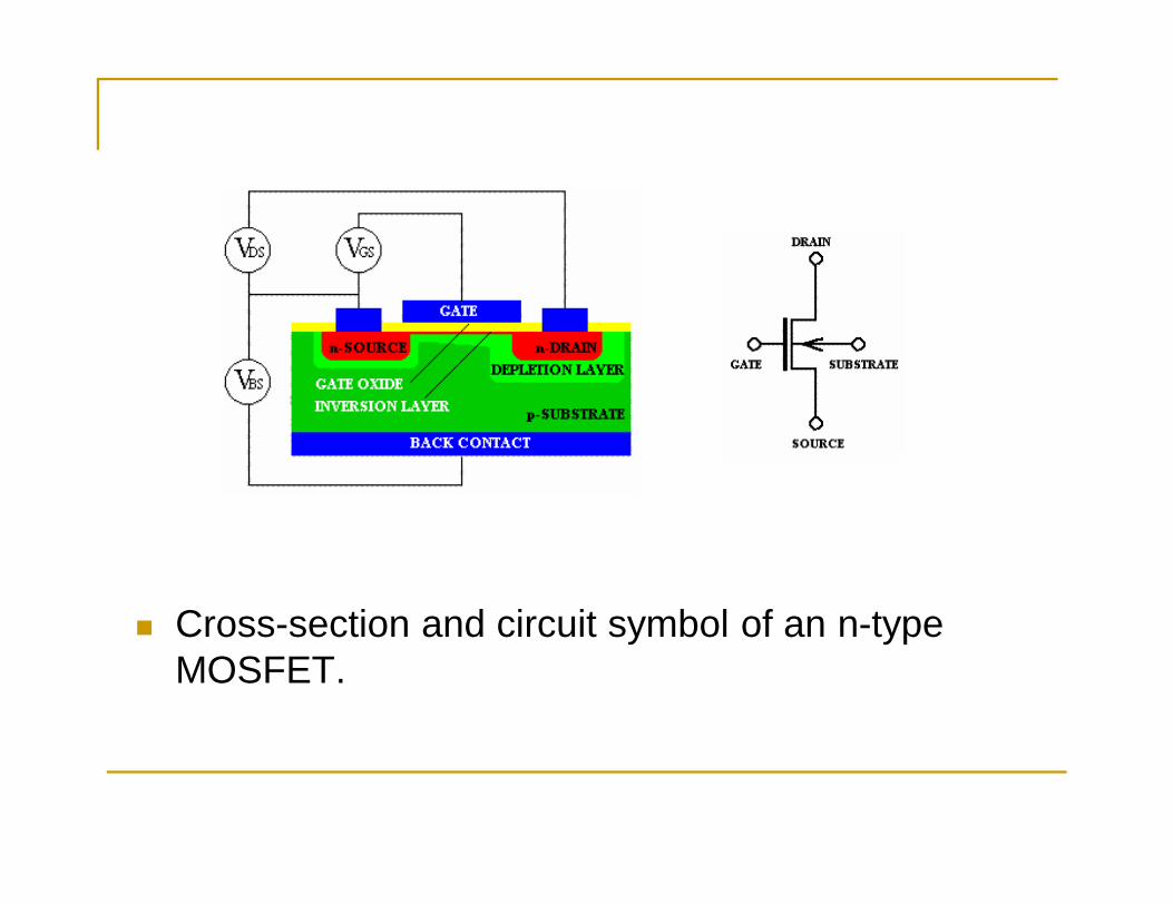
Cross-section and circuit symbol of an n-type MOSFET.
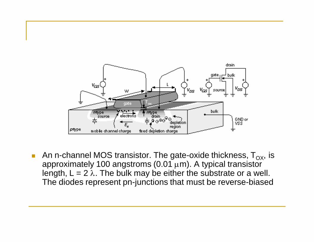
An n-channel MOS transistor. The gate-oxide thickness, TOX, is approximately 100 angstroms (0.01 m). A typical transistor length, L = 2 . The bulk may be either the substrate or a well. The diodes represent pn-junctions that must be reverse-biased

Basic MOSFET (p-channel)
These behave in a similar way, but they pass current when a -ve gate voltage creates an effective p-type channel layer under the insulator.
By swapping around p-type for n-type we can make pairs of transistors whose behaviour is similar except that all the signs of the voltages and currents are reversed.
Pairs of devices like this care called complimentarypairs.


In an n-channel MOSFET, the channel is made of n-type semiconductor, so the charges free to move along the channel are negatively charged (electrons).
In a p-channel device the free charges which move from end-to-end are positively charged (holes).
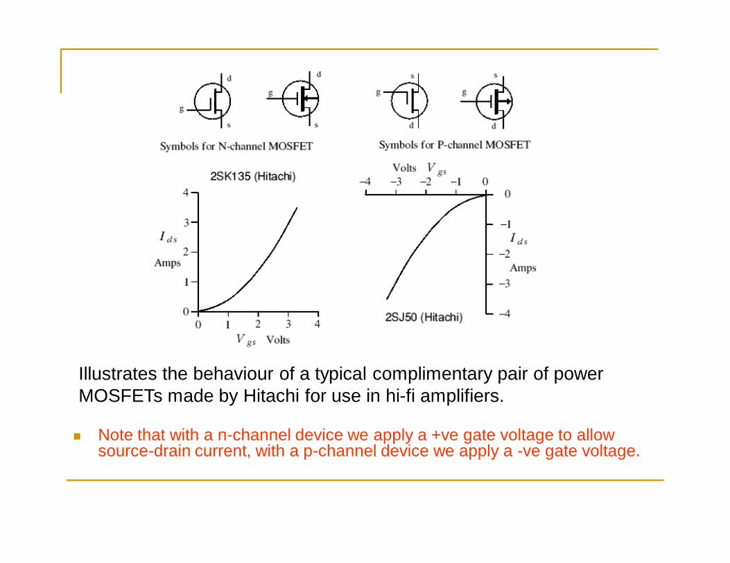
Note that with a n-channel device we apply a +ve gate voltage to allow source-drain current, with a p-channel device we apply a -ve gate voltage.
Illustrates the behaviour of a typical complimentary pair of power MOSFETs made by Hitachi for use in hi-fi amplifiers.
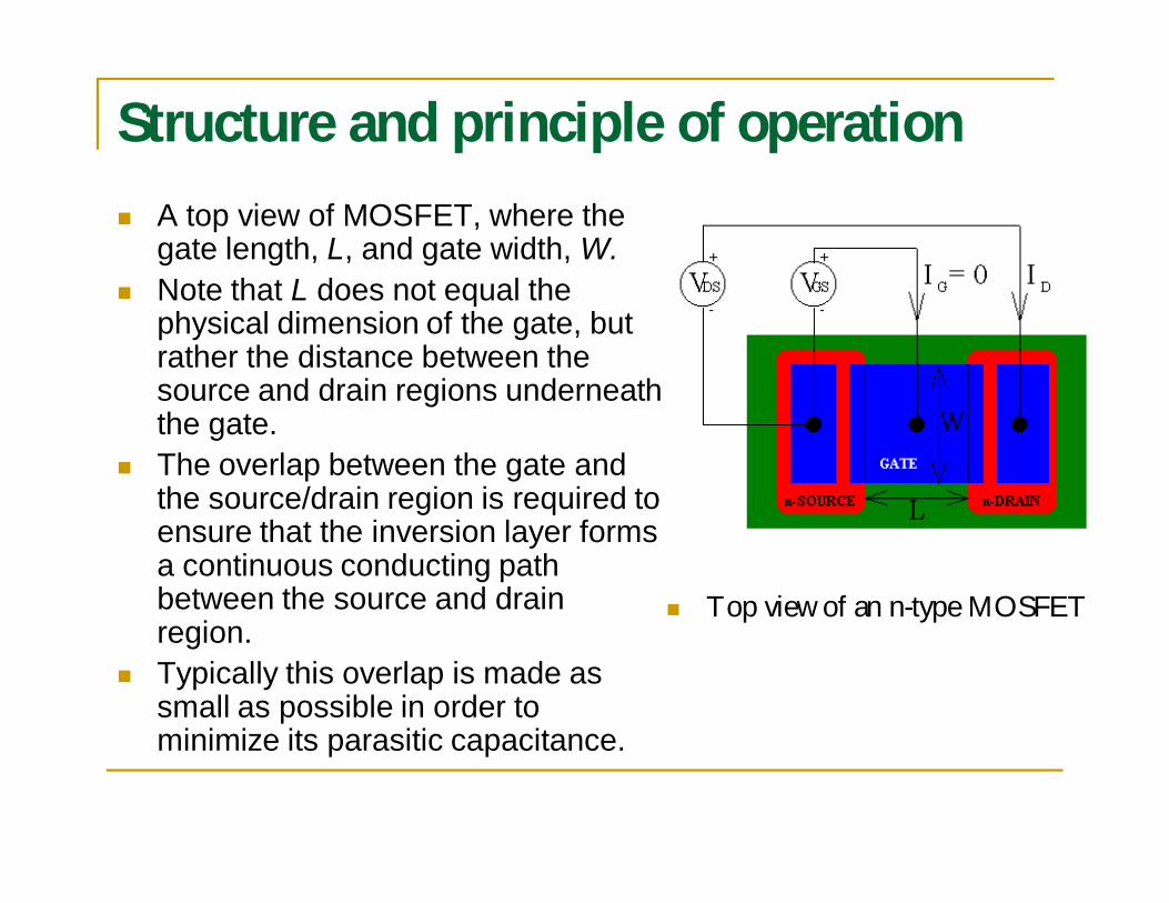
Structure and principle of operation A top view of MOSFET, where the
gate length, L, and gate width, W. Note that L does not equal the
physical dimension of the gate, but rather the distance between the source and drain regions underneath the gate.
The overlap between the gate and the source/drain region is required to ensure that the inversion layer forms a continuous conducting path between the source and drain region.
Typically this overlap is made as small as possible in order to minimize its parasitic capacitance.
Top view of an n-type MOSFET

MOSFET-Basic Structure
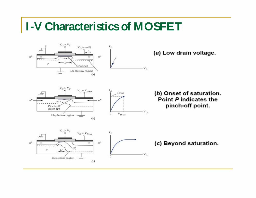
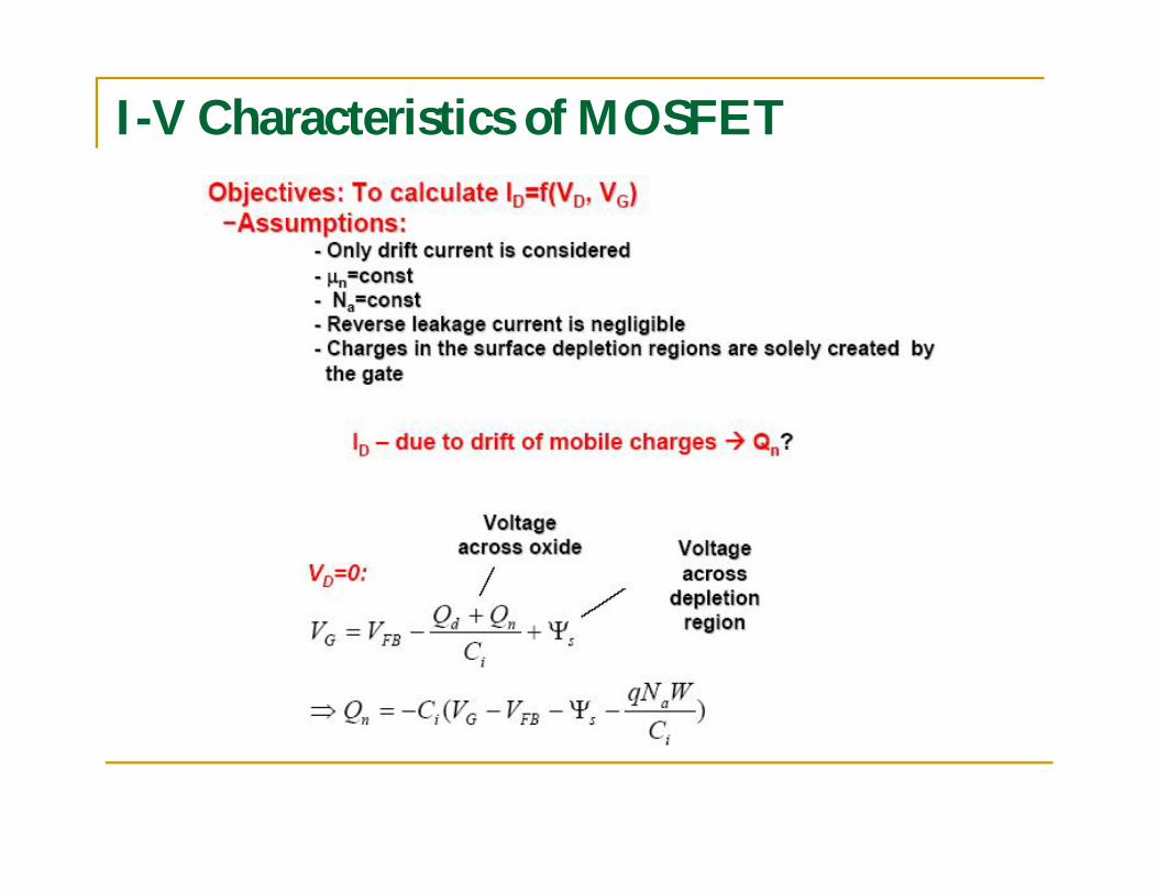
I-V Characteristics of MOSFET
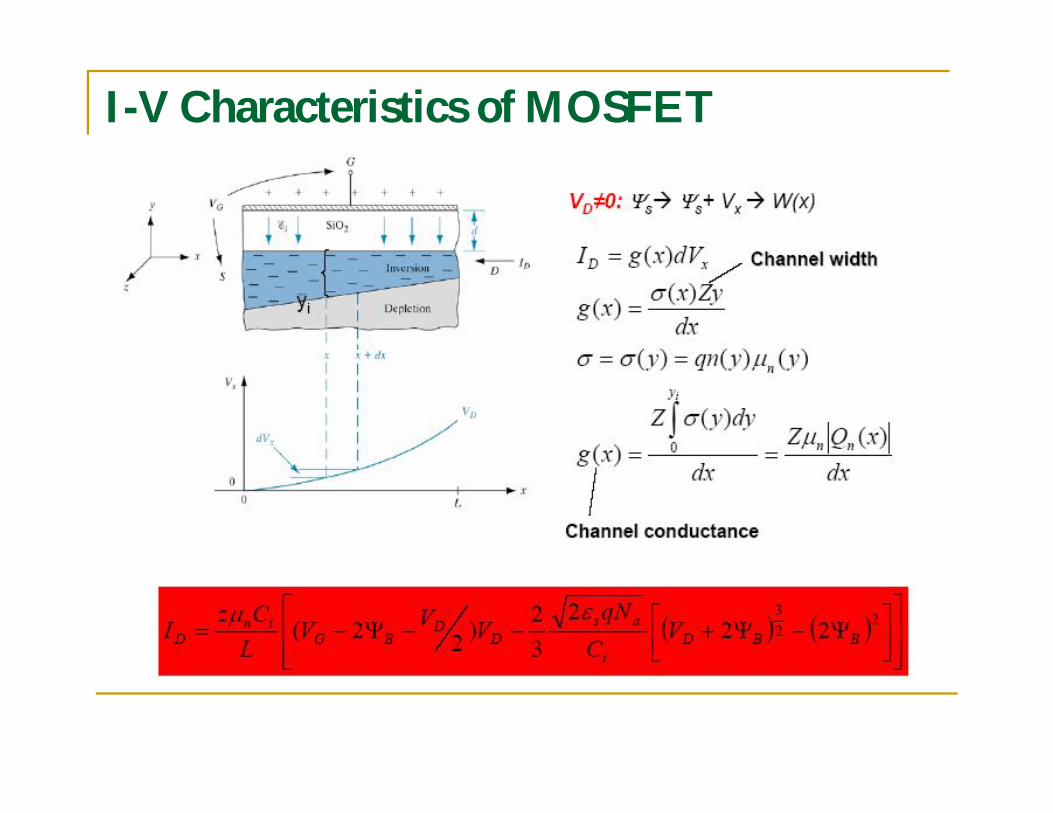
I-V Characteristics of MOSFET
I-V Characteristics of MOSFET
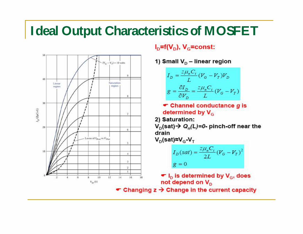
Ideal Output Characteristics of MOSFET
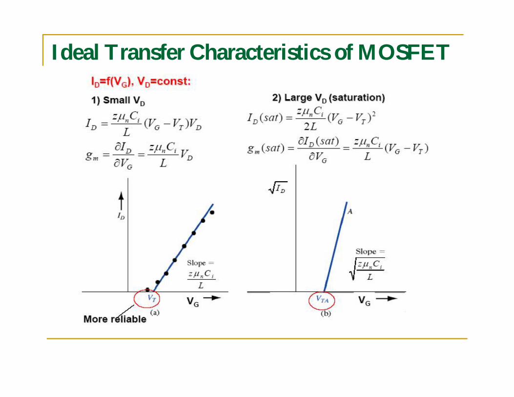
Ideal Transfer Characteristics of MOSFET

Types of MOSFET
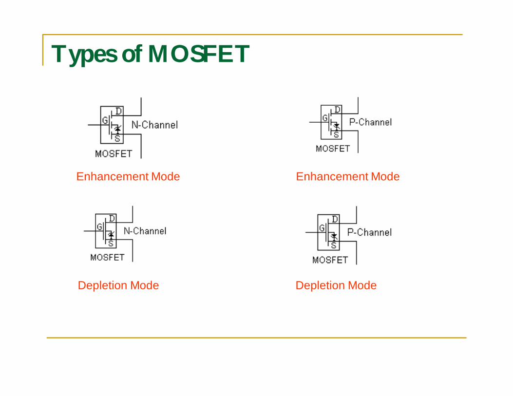
Types of MOSFET
Enhancement Mode Enhancement Mode
Depletion Mode Depletion Mode

Subthreshold region
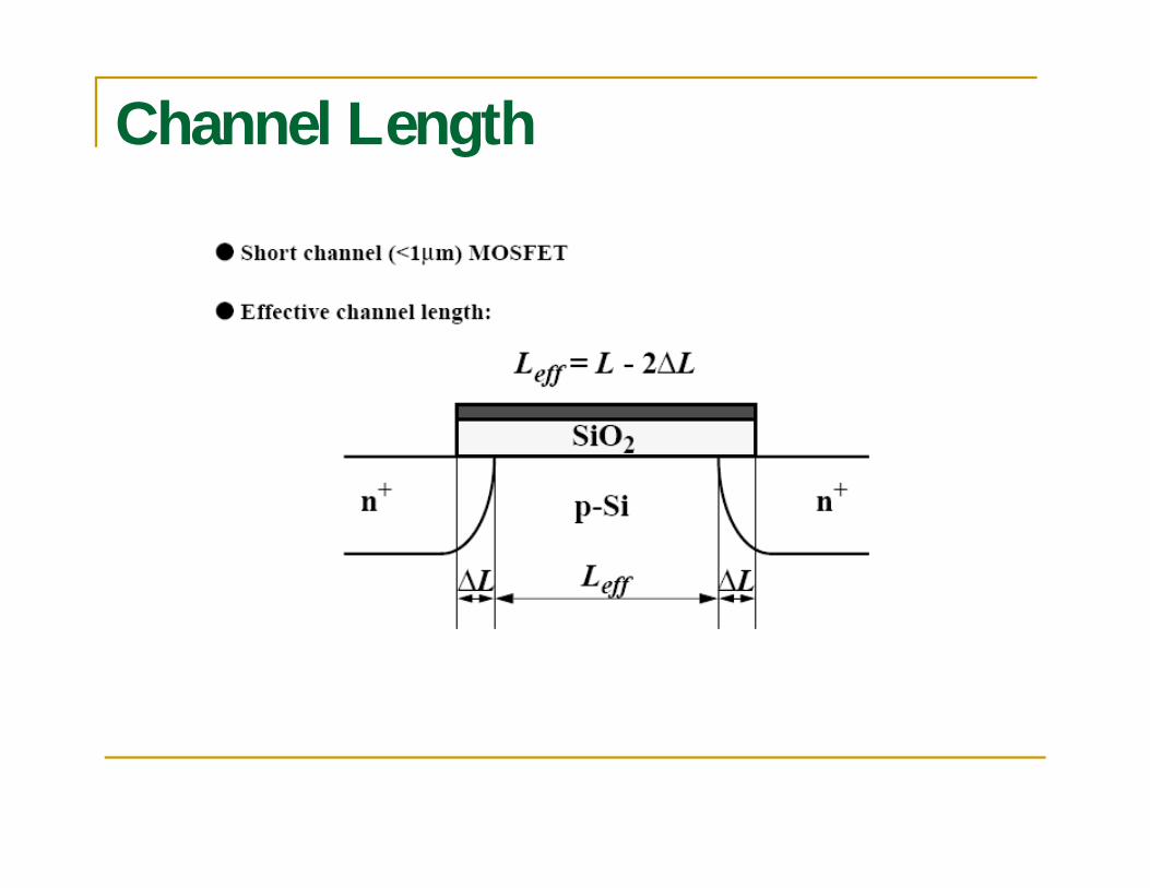
Channel Length

MOSFET Dimensions - Trend

MOSFET scaling scenario

Voltage Scaling
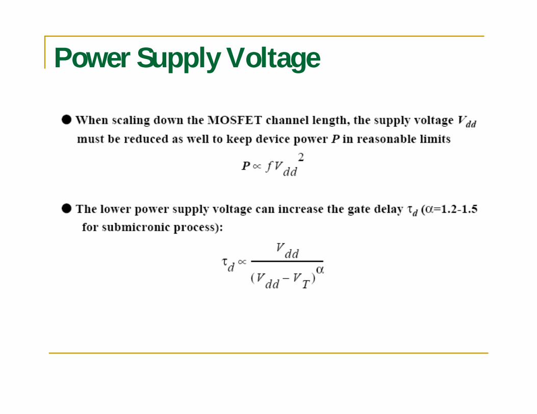
Power Supply Voltage
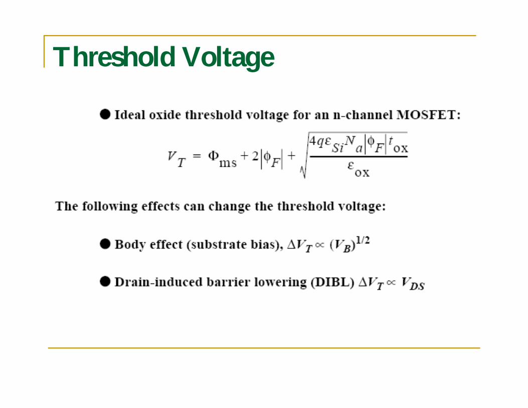
Threshold Voltage

Threshold Voltage
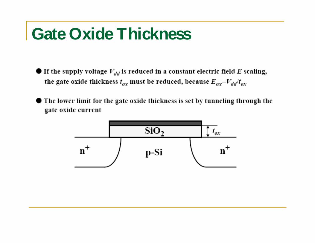
Gate Oxide Thickness

Channel Profile Evolution

MOSFET Capacitances

MOSFET Capacitances

Overlap Capacitance
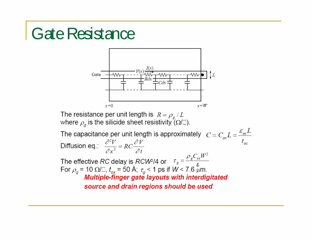
Gate Resistance
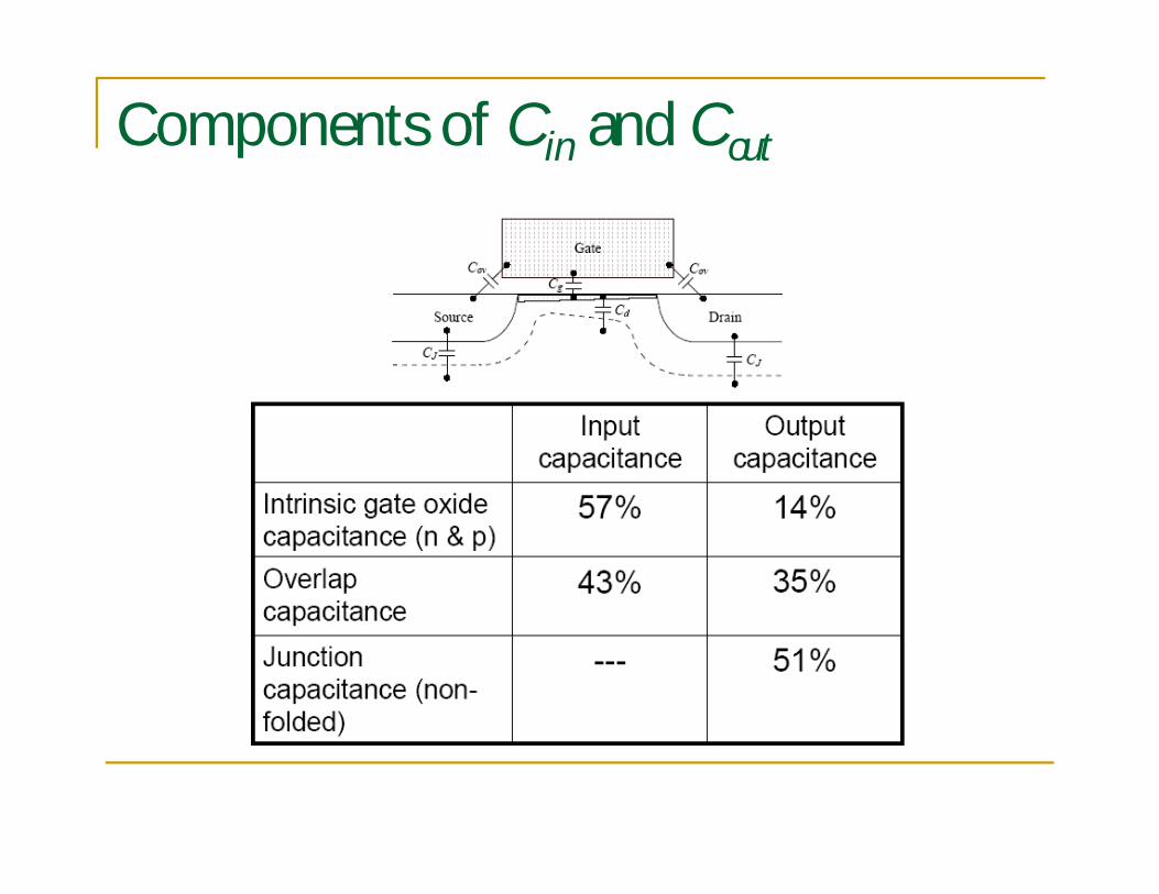
Components of Cin and Cout
New materials needed for scaling
Since the early 1980s, the materials used for integrated MOSFET on silicon substrates have not changed greatly.
The gate “metal” is made from highly-doped polycrystalline Si.
The gate oxide is silicon dioxide. For the smallest devices, these materials will
need to be replaced.
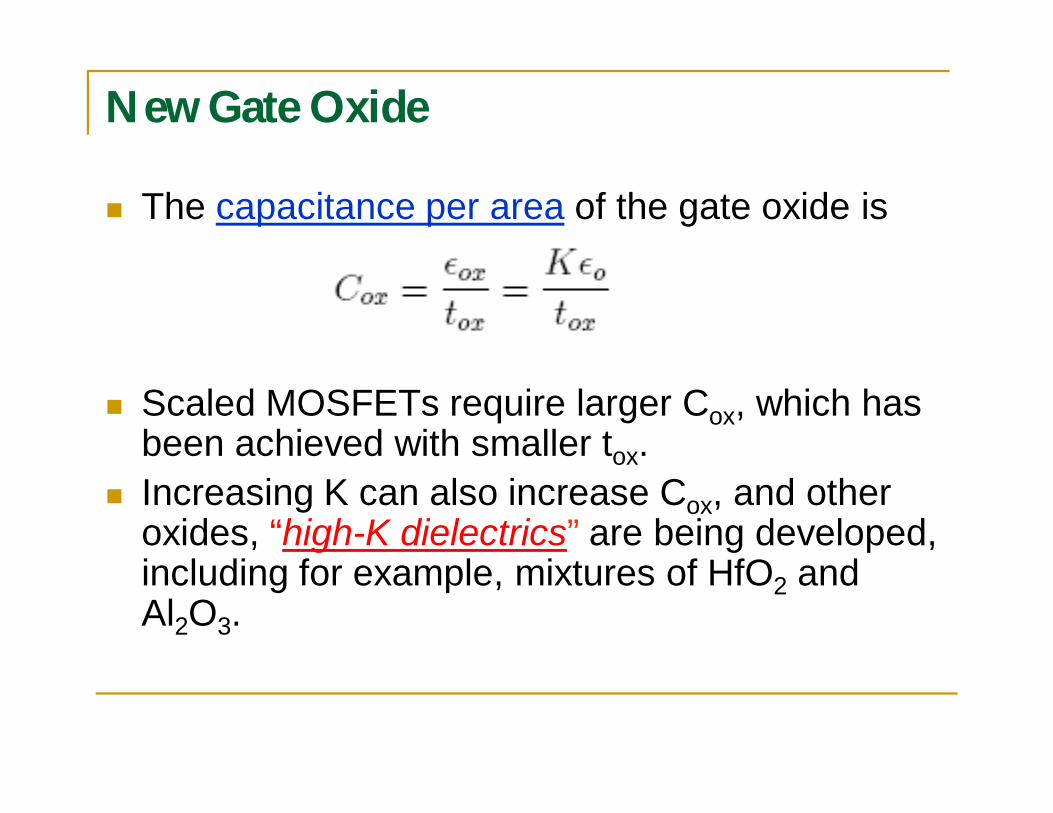
New Gate Oxide
The capacitance per area of the gate oxide is
Scaled MOSFETs require larger Cox, which has been achieved with smaller tox.
Increasing K can also increase Cox, and other oxides, “high-K dielectrics” are being developed, including for example, mixtures of HfO2 and Al2O3.

New Gate Metal
The doped polycrystalline silicon used for gates has a very thin depletion layer, approximately 1 nm thick, which causes scaling problems for small devices.
Others metals are being investigated for replacing the silicon gates, including tungstenand molybdenum.

Removing the substrate: Silicon on Insulator (SOI) For high-frequency circuits (about 5 GHz and
above), capacitive coupling to the Si substrate limits the switching frequency.
Also, leakage into the substrate from the small devices can cause extra power dissipation.
These problems are being avoided by making circuits on insulating substrates (either sapphireor silicon dioxide) that have a thin, approximately 100 nm layer of crystalline silicon, in which the MOSFETs are fabricated.

Silicon on Insulator (SOI)
SOI — silicon on insulator, refers to placing a thin layer of silicon on top of an insulator such as SiO2.
The devices will be built on top of the thin layer of silicon.
The basic idea of SOI is to reduced the parasitic capacitance and hence faster switching speed.

Silicon on Insulator (SOI)
Every time a transistor is turned on, it must first charge all of its internal (parasitic) capacitance before it can begin to conduct.
The time it takes to charge up and discharge (turn off) the parasitic capacitance is much longer than the actual turn on and off of the transistor.
If the parasitic capacitance can be reduced, the transistor can be switched faster —performance.

Silicon on Insulator (SOI)
One of the major source of parasitic capacitance is from the source and drain to substrate junctions.
SOI can reduced the capacitance at the source and drain junctions significantly — by eliminating the depletion regions extending into the substrate.

SOI CMOS
Silicon-on-insulator CMOS offers a 20–35% performance gain over bulk CMOS.
As the technology moves to the 0.13-µm generation, SOI is being used by more companies, and its application is spreading to lower-end microprocessors and SRAMs.
Some of the recent applications of SOI in high-end microprocessors and its upcoming uses in low-power, radio-frequency (rf) CMOS, embedded DRAM (EDRAM), and the integration of vertical SiGe bipolar devices on SOI are described.
IBM J Res. Dev., Vol. 46, No. 2/3, 2002

IBM J Res. Dev., Vol. 46, No. 2/3, 2002

Illustrations of silicon transistors
a, A traditional n-channel MOSFET uses a highly doped n-type polysilicon gate electrode, a highly doped n-type source/drain, a p-type substrate, and a silicon dioxide or oxynitride gate dielectric. b, A silicon-on-insulator (SOI) MOSFET is similar to the traditional MOSFET except the active silicon is on a thick layer of silicon dioxide. This electrical isolation of the silicon reduces parasitic junction capacitance and improves device performance. c, A finFET is a three-dimensional version of a MOSFET. The gate electrode wraps around a confined silicon channel providing improved electrostatic control of the channel electrons.
nature nanotechnology, 2 (2007) 25
Related Documents