Metal Oxide Nanostructures; Synthesis, Characterizations and Applications * 1 S.C. Singh, 2 D.P. Singh, 3 J. Singh, 3 P.K. Dubey, 3 R.S. Tiwari and 3 O.N. Srivastava 1 National Centre for Plasma Science and Technology (NCPST), School of Physical Sciences, Dublin City University, Dublin-9, Ireland 2 Thin Film Nanotechnology Laboratory, Department of Physics, Southern Illinois University, Carbondale, USA 3 Condensed Matter Physics & Hydrogen Lab., Department of Physics, Banaras Hindu University, Varanasi - 221005, INDIA *[email protected] ; Phone Number: +353-1700-7787

Metal Oxide Nanostructures Synthesis Characterizations and Applications (1)
Oct 28, 2015
Welcome message from author
This document is posted to help you gain knowledge. Please leave a comment to let me know what you think about it! Share it to your friends and learn new things together.
Transcript

Metal Oxide Nanostructures; Synthesis, Characterizations and Applications
*1S.C. Singh,
2D.P. Singh,
3J. Singh,
3P.K. Dubey,
3R.S. Tiwari and
3O.N. Srivastava
1National Centre for Plasma Science and Technology (NCPST), School of Physical Sciences,
Dublin City University, Dublin-9, Ireland 2 Thin Film Nanotechnology Laboratory, Department of Physics,
Southern Illinois University, Carbondale, USA
3Condensed Matter Physics & Hydrogen Lab., Department of Physics, Banaras Hindu
University, Varanasi - 221005, INDIA
Phone Number: +353-1700-7787
2
Table of Contents
1. Metal Oxide Nanostructures and their applications 2. Zinc Oxide Nanostructures; Synthesis, Characterizations and applications
2.1: Introduction 2.2: Crystal Structure and Physical Properties of Zinc Oxide
2.3: Synthesis of ZnO Nanostructures 2.3.1: Synthesis of ZnO Nanostructures by Solution routes 2.3.1.1: Precipitation Method 2.3.1.2: Hydrothermal Method 2.3.1.3: Solvothermal Method 2.3.1.4: Sol-gel Method 2.3.1.5: Micro emulsion Method 2.3.1.6: Combustion Synthesis 2.3.1.7: Electrochemical Synthesis 2.3.1.8 Sonochemical method 2.3.1.9 Laser ablation on solid liquid interface 2.3.2: Gas phase methods 2.3.2.1: Chemical Vapor Deposition (CVD) 2.3.2.2: Physical Vapor Deposition 2.3.2.3: Spray Pyrolysis Deposition 2.4: Applications of Zinc Oxide
2.4.1: Semiconductor nanolasers 2.4.2: Light emitting diodes (LEDs)
2.4.3: Solar Cells and light detectors 2.4.4: Electronic device fabrication 2.4.5: Hydrogen generation and storage
2.4.6: Sensors 2.4.7: Water and Air Purification 2.4.5: Cancer Treatment 2.4.6: Generation of PV Electricity 2.4.7: Air Purification
2.4.8: Biological and medical Application 2.4.9: Other Applications 2.5: Summary
3. Cuprous Oxide (Cu2O) Nanostructures; Synthesis, Characterizations and applications 3.1 Introduction 3.2 Crystal Structure and Physical Properties of Cuprous Oxide 3.3 Synthesis of Cu2O Nanostructures
3.3.1 Synthesis of Cu2O Nanostructures by Electrodeposition
3.3.2 Synthesis of Cu2O Nanostructures by Anodic Oxidation
3.3.3 Synthesis of Cu2O Nanostructures by Chemical Methods
3.3.4 Synthesis of Cu2O Nanostructures by Hydrothermal Process
3.4 Applications of bulk Cuprous Oxide
3.5 Application of different Cuprous Oxide Nanostructures
3
3.6 Summary
4. Titanium Dioxide Nanostructures; Synthesis, Characterizations and applications 4.1: Introduction
4.2: Crystal Structure and Physical Properties of Titanium Dioxide 4.3: Synthesis of TiO2 Nanostructures 4.3.1: Synthesis of TiO2 Nanostructures by Solution routes 4.3.1.1: Precipitation Method 4.3.1.2: Solvothermal Method 4.3.1.3: Hydrothermal Method 4.3.1.4: Sol-gel Method 4.3.1.5: Microemulsion Method 4.3.1.6: Combustion Synthesis 4.3.1.7: Electrochemical Synthesis 4.3.1.8: Laser ablation on solid liquid interface 4.3.2: Gas phase methods 4.4.1: Chemical Vapor Deposition (CVD) 4.4.2: Physical Vapor Deposition 4.4.3: Spray Pyrolysis Deposition 4.4.4: Other Gas Phase Methods 4.4: Applications of Titanium Dioxide 4.4.1: Photoelectrochemical generation of Hydrogen (solar Hydrogen) 4.4.2: Water Purification 4.4.3: Self Cleaning Surfaces 4.4.4: Sensors 4.4.5: Cancer Treatment 4.4.6: Generation of PV Electricity 4.4.7: Air Purification 4.4.8: Other Applications 4.5: Summary
5. Over all conclusion
6. Future prospects
7. References
Table Captions
Tables
Figure captions
Figures
4
Recently, scientific and research community have shown their great interest on metal oxide
nanostructures and their applications due to their easy, safe, environmental friendly, cheap
synthesis procedure and technological applications in the fabrication of devices for energy
harvesting and storage, photonics, sensors as well as medical and biological applications. Metal
oxides specially, oxide nanostructures of zinc, copper and titanium can be fabricated in various
morphologies such as nanoparticles, cubes, cuboids, circular and hexagonal discs, nanorods,
nanowires, tapes, belts, tetra pods, flowers using various cheap physical and chemical routes in
powder, colloid as well as nanostructures films phase. They can be fabricated on any type of
substrates such as metals, semiconductors, crystalline as well as amorphous, polymers, and
flexible plastics unlike other III-V semiconductor and silicon, which requires specific and costly
substrates. Now a days, these metal oxide nanostructures are widely used in the fabrication of
cheap and efficient solar cells, light detectors, nano-lasers, nano-generators, sensors and
electronic devices such as transistors and FETs. If zinc oxide nanostructures have highest
potential as nanolasers, nanogenerators to convert mechanical energy into electrical and LEDs
then titanium dioxide have largest potential into solar cells and environmental purifications,
while cuprous oxide has a lot of potential in the biological, medical and fabrication of electronic
devices. This review chapter is devoted to the various physical and chemical routes of the
fabrication of zinc, copper and titanium oxide nanostructures and their applications. Due to the
availability of cheap and versatile routes of fabrication of metal oxide nanostructures, they may
be treated as cheap replacement of silicon and gallium nitride based costly devices.

5
1. Metal Oxide Nanostructures and their applications
Nanostructures of metal Oxides have shown their revival of interest in the fabrication of
energy saving and harvesting devices such as Lithium ion batteries [1-5], fuel cells [6-10], solar
cells [11-37], transistors/FETs [38-48], Light emitting devices (LEDs) [49-64], hydrogen
production by water photolysis and its storage [65-83], water and air purification by degradation
and adsorption of organic/inorganic pollutants and toxic gases [84- 104], environmental
monitoring by their applications in the fabrication of gas, humidity and temperature sensors
[105- 136], UV-screening [137,138] and photodetectors [139-148]. Instead of these they have
also fabulous applications in biological and medical sciences such as drug delivery, cancer
treatments, fluorescent imaging, bio labeling and bio tagging etc [149-156]. Oxides of transition
metals have strong ferromagnetism with high Curie temperature and are used as magnetic read,
write heads and data storage devices [157-166]. Transition metal doped active oxides such as
ZnO, CuO, TiO2, Al2O3 etc. [167-177] are called diluted magnetic semiconductors (DMS) and
are applicable in the fabrication of spin based electronic devices i.e. Spintronics. Similarly rare
earth elements such as Eu, Nd, Sm, Tb doped metal oxides are usually used as phosphor
materials for fabrication of LEDs, displays and laser materials [178-187]. Metal oxides are
expected replacement and alternative of silicon and metal nitride based expensive electronic
devices and ICs. Recently oxide based nanomaterials such as ZnO, TiO2, CuO2 and so on have
revolutionized the nanomaterials research because of the availability/possibility of soft chemical
synthesis besides tremendous application potential. One of the salient features of these oxide
nanomaterials is the bio compatibility which opens an avenue for interdisciplinary research to
have better bridge up between physicist and biotechnologist. Binary semiconducting oxides, such
as ZnO, TiO2, CuO2/Cu2O, SnO2, In2O3, and CdO, have distinctive properties and are now
widely used as transparent conducting oxide materials [187,188] and sensors [105-136]. Such as
fluorine doped SnO2 film have potential application in architectural glass applications due to its
low emissivity for thermal infrared heat [189]. SnO2 nanomaterials are regarded as one of the
most important sensor materials for detecting leakage of several inflammable gases owing to
their high sensitivity to low gas concentrations [190]. Indium-doped tin oxide (In:SnO2, ITO)
film is an ideal material for flat panel displays because of its high electrical conductivity and
6
high optical transparency [191- 193], and ZnO is regarded as an ideal alternative material for
ITO because of its lower cost and easier etchability [194]. This chapter deals with different
methods of synthesis, characterization and applications of oxides nanostructures of zinc, copper
and titanium metals.
2. Zinc Oxide Nanostructures; Synthesis, Characterizations and applications
2.1: Introduction:
Recently scientific community has shown their revival of interest in Zinc oxide as a
cheap replacement of Si and GaN and regarded it as a “future promising material”. Zinc oxide is
an n- type, direct wide band gap semiconductor material having several applications in UV/blue
optoelectronics [52-64, 143-148], transparent electronics [42-48], spintronics [169-177] and
sensor applications [117-136]. Zinc oxide in its bulk polycrystalline form has been commonly
used in a wide range of applications such as sunscreen, ointments, facial powders, catalyst,
lubricant additives, paint pigments, piezoelectric transducers, varistors, and as a transparent
conducting electrodes. It has direct band gap energy of 3.40 eV, which makes its transparency in
the visible region and most of the activity in the UV/blue region. Higher exciton binding energy
of zinc oxide (∼60 meV) as compared to GaN (∼24 meV) enhances its luminescence efficiency.
In spite of higher exciton binding energy zinc oxide has a lot of other virtues over GaN including
its ability to easily grow on the single crystal substrate, low threshold value and bio
compatibility. Zinc oxide is widely used for the fabrication of transistors and FETs [42-48], light
emitting diodes [52-64], dye sensitized, hybrid and quantum dot solar cells [15-35] and
nanogenerators [197-203]. It is the most promising inorganic oxide, which is widely used for
fabrication of devices and other applications. Due to the advanced technological applications,
high quality of zinc oxide nanostructures are greatly demanded, which induces world wide
research and development on the synthesis and application of zinc oxide nanostructures.
2.2: Crystal Structure and Physical Properties of Zinc Oxide:
At normal temperature and pressure zinc oxide exhibit wurtzite crystal structure, which
is the hexagonal lattice with space group P63mc [Figure 1 (a)]. Instead of wurtzite, it also
crystallizes into zincblende [Figure 1(b)] and rocksalt structures [Figure 1 (c)] at different
experimental conditions. Lattice structure of zinc oxide is combination of two interconnected
sublattices of Zn2+ and O2- in such a manner that each of the zinc atom is surrounded by four
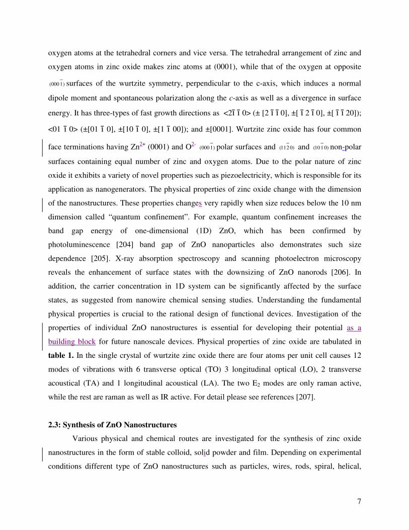
7
oxygen atoms at the tetrahedral corners and vice versa. The tetrahedral arrangement of zinc and
oxygen atoms in zinc oxide makes zinc atoms at (0001), while that of the oxygen at opposite
(000 1)−
surfaces of the wurtzite symmetry, perpendicular to the c-axis, which induces a normal
dipole moment and spontaneous polarization along the c-axis as well as a divergence in surface
energy. It has three-types of fast growth directions as <2ī ī 0> (± [2 ī ī 0], ±[ ī 2 ī 0], ±[ ī ī 20]);
<01 ī 0> (±[01 ī 0], ±[10 ī 0], ±[1 ī 00]); and ±[0001]. Wurtzite zinc oxide has four common
face terminations having Zn2+ (0001) and O2- (000 1)−
polar surfaces and (112 0)−
and (10 1 0)−
non-polar
surfaces containing equal number of zinc and oxygen atoms. Due to the polar nature of zinc
oxide it exhibits a variety of novel properties such as piezoelectricity, which is responsible for its
application as nanogenerators. The physical properties of zinc oxide change with the dimension
of the nanostructures. These properties changes very rapidly when size reduces below the 10 nm
dimension called “quantum confinement”. For example, quantum confinement increases the
band gap energy of one-dimensional (1D) ZnO, which has been confirmed by
photoluminescence [204] band gap of ZnO nanoparticles also demonstrates such size
dependence [205]. X-ray absorption spectroscopy and scanning photoelectron microscopy
reveals the enhancement of surface states with the downsizing of ZnO nanorods [206]. In
addition, the carrier concentration in 1D system can be significantly affected by the surface
states, as suggested from nanowire chemical sensing studies. Understanding the fundamental
physical properties is crucial to the rational design of functional devices. Investigation of the
properties of individual ZnO nanostructures is essential for developing their potential as a
building block for future nanoscale devices. Physical properties of zinc oxide are tabulated in
table 1. In the single crystal of wurtzite zinc oxide there are four atoms per unit cell causes 12
modes of vibrations with 6 transverse optical (TO) 3 longitudinal optical (LO), 2 transverse
acoustical (TA) and 1 longitudinal acoustical (LA). The two E2 modes are only raman active,
while the rest are raman as well as IR active. For detail please see references [207].
2.3: Synthesis of ZnO Nanostructures
Various physical and chemical routes are investigated for the synthesis of zinc oxide
nanostructures in the form of stable colloid, solid powder and film. Depending on experimental
conditions different type of ZnO nanostructures such as particles, wires, rods, spiral, helical,
8
flower, tetrapod etc. are observed in both physical as well as chemical routes. There are some
advantages and shortcomings of each of the routes. Particular routes should be employed for the
synthesis of zinc oxide nanostructures for particular applications. Here we describe various
physical and chemical routes for the synthesis of various types of zinc oxide nanostructures.
2.3.1: Synthesis of ZnO Nanostructures by Solution routes
It is the widely used method for the synthesis of zinc oxide nanostructures. It deals with
the reaction of one solution containing zinc source such as acetate, nitrate, chloride etc. of zinc
with the other solution containing some reducing agent such as sodium or ammonium
hydroxide/nitrates/carbonates in the presence of stabilizing agents. Several solution based routes
such as precipitation, solvothermal, hydrothermal, sol-gel, micro-emulsion, combustion,
electrochemical, sono-chemical etc. are available for the synthesis of zinc oxide nanoparticles.
These routes are separately discussed in the following subsections in details.
2.3.1.1: Precipitation Method
In the precipitation method particular concentration of zinc precursor (nitrate or acetate or
carbonate of zinc) placed at particular reaction temperature. When temperature of the precursor
solution get stabilizes, stoichiometric solution of sodium or ammonium hydroxide is added
immediately under vigorous stirring. Stirring and heating of the reaction mixture is continued for
3-4 hours after addition of hydroxide solution. Temperature of reaction mixture is varied in
order to synthesize zinc oxide nanostructures of different size, shape and morphologies. Zinc
oxide precipitate is separated from the reaction mixture by centrifugation and washed with the
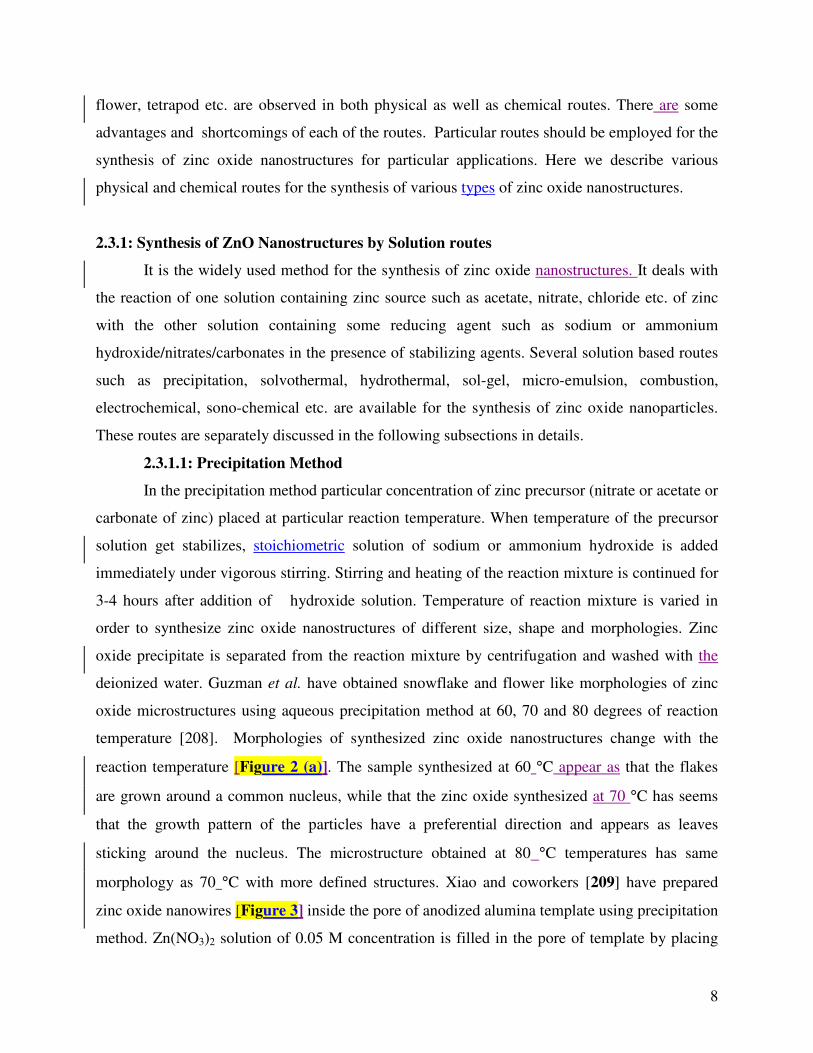
deionized water. Guzman et al. have obtained snowflake and flower like morphologies of zinc
oxide microstructures using aqueous precipitation method at 60, 70 and 80 degrees of reaction
temperature [208]. Morphologies of synthesized zinc oxide nanostructures change with the
reaction temperature [Figure 2 (a)]. The sample synthesized at 60 °C appear as that the flakes
are grown around a common nucleus, while that the zinc oxide synthesized at 70 °C has seems
that the growth pattern of the particles have a preferential direction and appears as leaves
sticking around the nucleus. The microstructure obtained at 80 °C temperatures has same
morphology as 70 °C with more defined structures. Xiao and coworkers [209] have prepared
zinc oxide nanowires [Figure 3] inside the pore of anodized alumina template using precipitation
method. Zn(NO3)2 solution of 0.05 M concentration is filled in the pore of template by placing

9
the template in the solution and placed horizontally on the outlet of conical flask containing
ammonia solution. The template is kept into the tube furnace at 150 °C for 1 hour and finally
cooled down to room temperature, which causes growth of mesoporous zinc oxide nanowires
inside the pore of alumina template. Suwanboon et al. [210] have synthesized zinc oxide
nanostructures using zinc acetate as precursor solution, different concentrations of PVP to
control the growth and coagulation process of synthesized intermediate product and sodium
hydroxide as reducing agent. Variations are brought in terms of concentrations of zinc acetate
and PVP and reported that concentration of zinc acetate does not affect the size of zinc oxide
particles but the its shape changes from plate like to sphere with the increase precursor
concentrations. Crystallite size of the zinc oxide particles decreases with the increase of PVP
concentrations. In another study solutions of hydrated zinc chloride and anhydrous ammonium
carbonate was mixed under intensive stirring, which causes synthesis of zinc hydroxy carbonate
precursor [211]. Annealing of thus obtained precursor at 300°C for different times produces zinc
oxide particles of various grain sizes. Taubert and co-workers [212] have synthesized zinc
dumbbell shaped zinc oxide nanostructure [Figure 4] using precipitation route. In a typical
synthesis process 446 mg of Zn(NO3)2.6H2O and 12 mg of polymers P(EO-b-MAA) or P(EO-b-
SSH) are dissolved in 100 ml of deionized water and subjected to heat at 90 °C. Solution of 210
mg of hexamethylene tetramine in 2 ml of deionized water is added to the continuously stirred
solution. The reaction mixture at 90 °C for 90 minutes and cooled by ice bath. The white
precipitate was separated by centrifugation washed with water and ethanol and dried in vacuum
at 60°C. Zinc acetate, triethanolamine solution in ethanol and n-propylamine solution in ethanol
is also used to prepare zinc oxide nanoparticles by precipitation method [213].
2.3.1.2: Hydrothermal Method
Hydrothermal is an aqueous solution base wet chemistry method for the synthesis of zinc
oxide nanoparticles. In a typical reaction process aqueous solution of any of the zinc precursor is
placed in thermal reactor. Mostly Teflon lined stainless steel sealed chamber named as
“hydrothermal bomb” is used as thermal reactor. The temperature of reaction mixture and time
of the hydrothermal treatment is the key variable parameters to get various types of zinc oxide
nanostructures. Nature and concentration of zinc precursor, solvent used, nature and
concentration of surfactant of polymers used, reaction temperature, reaction duration, pH of the
10
reaction mixture are some of the parameters to control size, shape, morphology and crystallinity
of nanoparticles synthesized by hydrothermal route. Ohara et al. [214] used a special reactor in
which the reaction solution is used to flow through the tube furnace. The aqueous solution of
zinc nitrate was fed into the reactor by high pressure pump at a flow rate of 2 cm3/min and mixed
with supercritical water system placed at 450°C at the flow rate of 10 cm3/min and the reaction
mixture was heated at 400°C under 30 MPa pressure for about 10 sec. The fluid was rapidly
quenched by the addition of KOH solution at the rate of 10 cm3/min and cooling with external
water jacket. Rod shaped zinc oxide nanoparticles are collected by using the upstream inline
filter. Li et al. [215] have synthesized zinc oxide nanorods and nanowires by PEG assisted
hydrothermal route. They used aqueous solution of zinc acetate and added solution of sodium
hydroxide with stirring. 2 ml solution of obtained mixture with 5 ml PEG and absolute ethanol
(upto 90% of the total volume) was loaded in the Teflon lined autoclave, and was being sealed
and maintained at 140°C for 24 hours and allowed to cool to room temperature. The precipitate
was filtered off, washed several times with ethanol and distilled water and dried at 60°C in
vacuum oven [Figure 5]. Similarly Greene et al [216] have also added aqueous solution of zinc
acetate (4 mmol) to 15 ml of triocetylamine and 3g of oleic acid (12 mmol) at room temperature
and resultant mixture is heat treated at 286°C to get zinc oxide nanorods and particles. When the
temperature is maintained at 286°C for 1 hour under N2 flow zinc oxide nanorods are produced,
while zinc oxide nanoparticles are precipitated by adding ethanol after the cooling of reaction
mixture at room temperature. In another experimental procedure [217] 14.87 g of zinc nitrate
[Zn(NO3)2.6H2O] and 40 g of NaOH was dissloved in 100 ml of distilled water. 3 ml of above
solution was mixed with 0-5 ml of distilled water and 25-30 ml of ethanol, followed by the
addition of 5-6 ml of ethylenediamine and the resultant solution was homogenized with
ultrasonic bath treatment for 20-40 min. The solution was transferred into teflon lined autocalve
and heat treated 180°C for 20 hours. On the completion of reaction process zinc oxide nanorods
of 50 nm diameters are obtained by centrifugation, which was washed with deionized water prior
to characterization. Wang and Gao [218] used aqueous solution of zinc nitrate (1M), zinc
carbonate (1M) and 0.4%PEG to synthesize zinc oxide nanowires using hydrothermal route. 10
ml solution of zinc nitrate was added into 20 ml solution of zinc carbonate with vigorous stirring
and the precipitate was filtered, rinsed with distilled water and dispersed into 70 ml of PEG
solution. The resultant suspension was transferred in the teflon lined stainless steel autoclave of
(a) (a)
11
100 ml and heated at 200° for 10 hours. After the reaction the zinc oxide was separated by
centrifugation and washed. Lu et al [219] studied influence of alkaline sources on the structural
and morphological properties of hydrothermally synthesized zinc oxide powders [Figure 6].
Molar solutions of different alkaline source such as mono, di, tri ethanolamine (EA) and NH4OH
were added separately into aqueous solution of zinc nitrate (0.1M, 250 ml) and resultant mixture
was transferred into teflon lined stainless steel autoclave placed and heated at 100°C for 1h with
mechanical stirring at the rate of 300 rpm. After completion of reaction the products was
separated by centrifugation, washed several times and dried at 60°C temperatures. ZnO sample
synthesized with ammonium hydroxide has c-oriented growth of the nanorods, when it is
replaced by mono, di- and tri- ethanolamine crystallinity as well as aspect ratio decreases from
mono to tri. Spherical ZnO particles are produced with trietahnolamine [Figure 6 a-d). With the
addition of NH4OH in dietahnolamine, crystallinity as well as aspect ratio increases [Figure 6 e-
h]. In another set of experiments Lu and Yeh [220] have reported effect of reaction time, reaction
temperature and pH of the mixture on the size, shape and morphology of hydrothermally
synthesized zinc oxide nanopowders. They used addition of ammonia solution into 0.5 M
aqueous media of zinc nitrate and obtained precipitate was filtered, washed and filled into teflon
lined stainless steel autoclave with the addition of extra 250 ml distilled water. pH of the mixture
is varied in the range of 9-12 with ammonia solution, hydrothermal temperature was 100-200 °C
and time of heat treatment was varied from 0.5 to 2h. They concluded that reaction time does not
make any effect, while raising the reaction temperature above 100°C slightly reduces the particle
size and yield, while increase of pH from 9 to 12 changes shape of zinc oxide from ellipsoidal to
rod like structures with the increase in crystallinity and particle size but decrease in the yield.
Effect of nature of the solvent, used in the hydrothermal process, on the morphology of
synthesized zinc oxide nanopowders is investigated by Xu et al. [221]. They employed zinc
acetate as precursor and distilled water, KOH (0.25-2 mol/lit.) and ammonia solution (0.025-0.20
mol/lit.) as solvent for the synthesis of zinc oxide nanopowder with hydrothermal process. In the
procedure, 26 ml of solvent was added into teflon lined autoclave of 40 ml volume containing
zinc acetate solution (6.5 ml, 1M) with vigorous stirring. The autoclave was maintained at 200°C
for 2h and cooled to room temperature prior to filtering, washing and drying. They reported
synthesis of pencil like zinc oxide powder in pure water, while using KOH solution as solvent in
different concentrations produced different morphologies of zinc oxide nanostructures such as
12
twinned pyramidal, shortened prismatic, sheet and prismatic like etc. Ammonia solution of
different concentrations causes zinc oxide particles of ellipsoidal and long prismatic [Figure. 7]
shapes.
2.3.1.3: Solvothermal Method
Solvothermal synthesis route is very similar to the hydrothermal route, the only
difference is in the precursor solution which is usually non-aqueous or mixture of aqueous and
non-aqueous. Making use of the solvothermal route, one gains the benefits of both the sol-gel
and hydrothermal routes. So solvothermal synthesis allows for the precise control over size,
shape distribution and high crystallinity of zinc oxide nanoparticles or nanostructure. Reaction
temperature, reaction time, solvent type, surfactant type, precursor type are some of the
experimental parameters. There are number of reports on the synthesis of zinc oxide
nanostructures with solvothermal route employing different zinc precursors, different organic
solvents and reaction temperatures [222-228]. Zinc oxide nanorods of 80-800 nm diameter are
synthesized by Varghese et al [222] with the reaction between zinc acetate (300 mg), absolute
alcohol (4 ml) and ethylenediamine (6 ml) in 20 ml of stainless steel autocalve under
solvothermal conditions (300 °C for 20 h). Precipitate was filtered and washed with ethanol and
distilled water. Addition of Triton X-100 into the reaction mixture produces zinc oxide nanorods
of uniform 300 nm diameter, while addition of NH3 produces N doped zinc oxide nanorods.
Tonto et al. [223] have synthesized zinc oxide nanorods by reaction of zinc acetate in various
alcohols (1-butanol, 1-hexanol, 1- octanol and 1-decanol) under solvothermal conditions. The
aspect ratio of synthesize zinc oxide nanostructure increases with the increase of length of carbon
chain in the alcohol solvent and reported linear relationship of aspect ratio with the boiling point
of solvent. Crystallinity aspect ratio and quality of zinc oxide nanorods increases with the
concentration of hydrazenehydrate added in the autoclave containing pure zinc acetate powder
[224] in the solution of zinc acetate. Dev et al. [225] have synthesized zinc oxide nanostructures
by putting zinc oxide foils in the teflon lined stainless steel autoclave containing different ratios
of water and ethylenediamine (EN) and placed in furnace at 150-230 °C temperatures for 3-12 h.
The effect of reaction time, temperature and filling factor inside the autoclave on the size, shape,
morphology and optical properties of zinc oxide nanostructures were demonstrated. The relative
intensity of (002) peaks in the synthesized nanorods increases with the increase of EN in the 60
ml of water-EN system and reaches at maximum for 10 ml water and 50 ml EN. With the

13
addition of EN decreases the diameter and increases orientation of zinc oxide nanorods
significantly [Figure 8]. The sample produced in 10 ml water and 50 ml EN system is almost
perfectly aligned on the surface of zinc foil with 75-150 nm diameter and 2µm length. They have
also reported that average diameter and length of the nanorods increases with the reaction time.
In the similar study Lu et al. [226] have synthesized zinc oxide hierarchical nanostructurures by
placing zinc foils in the Water/EN system with 1:7 volume ratios with a small ratio of NaOH at
160 °C temperature [Figure 9]. They have also investigated morphological evolution of zinc
oxide nanostructures on the reaction time [Figure 10] and ratio of water to EN. Zhang et al [227]
used ethylene glycol (EG) as a solvent for the synthesis of zinc oxide microspheres consisting of
orderly and redical nanorods. Zinc chloride (1mmol) was dissolved into the 120 ml of EG and
sodium acetate (3.6 g) was added in the solution after 30 min. of stirring. The mixture was
transferred into autoclave at 200°C for 20hours. The precipitate was filtered and washed with
deionized water and ethanol [Figure 11]. Zinc oxide tubular nanostructures are synthesized by Li
and coworkers using zinc nitrate hexahydrate, sodium hydroxide, absolute alcohol and sodium
chloride by solvothermal route [228].
4.3.1.4: Sol-gel Method
Another solution based wet chemical route for the synthesis of zinc oxide nanostructures
is sol-gel method evolving a solution which acts as precursor for an integrated network (or gel)
of either discrete particles or network of polymers. Typical precursors are zinc alkoxides or zinc
chloride, which undergoes various forms of hydrolysis and poly-condensation reactions. The
formation of zinc oxide involves connecting the zinc centers with oxo (M-O-M) or hydroxo (M-
OH-M) bridges, therefore generating zinc-oxo or al-zinchydroxo polymers in solution. Thus, the
sol evolves towards the formation of a gel-like diphasic system containing both a liquid phase
and solid phase whose morphologies range from discrete particles to continuous polymer
networks. Zinc oxide monoliths were synthesized by Gao et al [229] by sol-gel route using
alcoholic zinc nitrate solution with propylene oxide as the gelatin initiator. In a typical reaction
process Zn(NO3)2.6H2O (0.8 mmol) was dissolved in the solvent and stirred to get the clear
solution to which 8mmol of propylene oxide was added with stirring. This solution was placed
undisturbed. Zinc oxide nanostructures on the silicon substrate are grown by Li et al. [230] using
sol-gel approach employing Zn(NO3)2.6H2O as zinc precursor, deionized water as solvent and
methenamine as stabilizing agent. The zinc precursor and methenamine solution were used in
14
equi-molar (0.01 mol/L) concentrations. After making homogeneous precursor solution using
magnetic stirring at 60 °C for 2 h it was placed in air for 24h to get homogeneous clear sol.
Neutral (pH=7) and acidic solution (pH=6, by adding HNO3) were used to get different zinc
oxide nanostructures. The cleaned and etched silicon substrate was immersed in the solution and
heated in the oven at 90°C for 2h. Thereafter Si was removed from the solution and baked in the
oven at 108°C followed by annealing in the quartz tube at 500 °C for 4h under O2 flow. Neutral
solution produces rods, while acidic generates rods as well as plate like structures [Figure 12]. In
another studies zinc oxide nanostructures are obtained by sol-gel route using 20 ml, 1M aqueous
solution of NaOH and 0.1 M aqueous solution of zinc acetate, which were mixed with magnetic
stirring at 50-60 °C temperature for 1h and kept at room temperature for 7days [231].
4.3.1.5: Microemulsion Method
Micro-emulsion is another important solution based method for zinc oxide synthesis.
Microemulsions are usually clear, stable, isotropic liquid mixtures of oil, water and surfactant,
frequently in combination with a co-surfactant. The aqueous phase may contain salt/salts of zinc
and/or other ingredients, and the "oil" may actually be a complex mixture of different
hydrocarbons and olefins. For the preparation of zinc oxide nanoparticles, particular
concentration of zinc salt [e.g. Zn (NO3)2] as the aqueous phase, has been commonly used to mix
another microemulsion containing the precipitation agent [e.g. NH4CO3] [232-236]. Continuous
collision of these micro-droplets leads to their coalescence and subsequent formation of insoluble
precipitate of zinc compound (in this case Zinc carbonate) in the droplet. The surfactant prevents
the growth and coagulation process of the carbonate particles. The synthesized zinc carbonate
particles undergoes washing with 1:1 solution of methanol and chloroform and heated to get zinc
oxide nanoparticles. Size, shape, distribution, morphology and hence properties of zinc oxide
nanoparticles synthesized by microemulsion method depends on the concentration and nature of
zinc salt, nature and concentration of reducing agent, type and concentrations of surfactant and
oil used to form microemulsion. Therefore choosing different type and concentrations of zinc
precursors, reducing agent, surfactant and oils one can synthesize zinc oxide nanostructures of
different size, shape and morphologies. Zhang et al [232] have synthesized 1D single crystalline
zinc oxide nanostructures using facile microemulsion method. In the typical reaction procedure
zinc acetate and sodium hydroxide was mixed in stochiometric ratio to get Zn(OH)4-2 precursor
solution. Thus obtained resultant precursor solution (1.2 ml), CTAB surfactant (1g), n-hexanol
15
cosurfactant (2 ml) and n-heptane (11.2 ml) solvent were mixed with various molar under
vigorous stirring ratio to get microemulsion based system, which was transferred to 25 ml of
Teflon lined stainless steel autoclave at a given temperature for certain time. Precipitate was
filtrated and washed with water and alcohol after cool down naturally upto room temperature and
dried in vacuum oven at 50-60 °C. They have reported growth and evolution of zinc oxide
nanostructures with reaction time [Figure 13]. Zinc oxide nanostructures with various
morphologies were prepared by Li et al [233] using microemulsion process utilizing heptane and
hexanol (mol ratio 3:1) as oil phase and Triton X-100 as a non-ionic surfactant. Calculated
amount of triton X-100 was added to the oil phase under stirring to get 0.2mol/L solution (ME).
Two microemulsions ME-1 and ME-2 containing different reactants was prepared. ME-1 was
obtained by adding 3 ml of 0.25 mol/L aqueous solution of Zn(NO3)2 containing different
concentrations of PEG 400 additives to 30 ml of ME. Addition of 3 ml of 0.5 mol/L aqueous
solution of NaOH resulted ME-2 reactant. ME-1 was slowly added to ME-2 under stirring and
resultant mixture was transferred into 100 ml of teflon lined stainless steel autoclave placed at
140°C for 14h. After completion of reaction autoclave was cooled naturally to room temperature,
precipitate was filtered, washed with water and ethanol and dried in air at 60°C. They have
synthesized zinc oxide nanostructures of different size (mean diameter 54.2, 70, 65, and 46.2
nm) and shapes (needle and spherical, column, column, and spherical) by varying the
concentrations (0, 12.5, 25, and 50 weight %) of PEG.
4.3.1.6: Combustion Synthesis
Combustion or burning is the sequence of exothermic chemical reactions between a fuel
and an oxidant accompanied by the production of heat and conversion of chemical species. Most
fuels of interest are organic compounds (especially hydrocarbon) in the gas, liquid or solid phase.
According to the phase of the fuel there are three types of combustion synthesis of nanomaterials
(a) solid phase combustion (b) solution combustion synthesis and (c) gas phase combustion
synthesis. Solution phase combustion out of the three is mostly used, while the gas phase
combustion is least. Jayalaxmi et al [237] have synthesized ZnO nanopowder using solution
combustion synthesis and employed 10g of zinc nitrate and 3.6 g of dextrose solution into 25 ml
of water. Glass vessel containing aqueous solution was placed on the hotplate for 15min. to form
a gel and placed into muffle furnace at 400°C for 5 min. The formed powder was highly
amorphous in nature. Zinc oxide nanostructures are synthesized by Alvarado-Ibarra et al. [238]

16
using solid as well as solution combustion methods. In a typical reaction process 0.2 g of
Zn(NO3)2.6H2O and 0.4g of urea was mixed and suspended in 1ml of distilled water. For solid
combustion the mixture was heated until all the water evaporated before placing it in the muffle
furnace, while for solution phase synthesis aqueous mixture was placed in the furnace operating
at 800 °C. SEM images of the zinc oxide nanostructures obtained by direct calcination of zinc
nitrate, solid combustion and solution phase combustion methods are illustrated [Figure 14].
Zinc oxide nano-tetrapod like structure is synthesized by Chen et al. [239] using melting
combustion method. The stainless steel container having a nozzle at its centre carrying bulk
metallic zinc was charged into an electric furnace and got melted into liquid, which flowed down
on the flame of O2 and C2H2 gas and burned to produce huge zinc fumes. The zinc fume was
carried by fan to the cooling collector and deposited as zinc oxide nano-tetrapod powder [Figure
15].
2.3.1.7: Electrochemical Synthesis
Electrochemistry, a method that employs deposition of a layer of metal/metal oxide on
the conducting electrode, was invented by Italian Chemist Luigi V. Brugnatelli [240]. First metal
oxide that was deposited electrochemically were thallium oxide [241] and zirconium oxide [242]
while electrochemical synthesis of zinc oxide was first time reported by Izaki and Omi [243] and
Peulon and Lincot [244]. Cathode potential, current density, deposition temperature, electrolyte
composition and concentration are some key parameters to control the size, shape, composition
and morphology of synthesized nanostructures. Number of papers on the electrochemical
deposition of zinc oxide is reported with variety of conducting electrodes such as transparent
semiconductors ITO [245], FTO [246], Metals electrodes such as Au [247], Sn [248], Pt [249],
Zn [250] and Cu [251], AAO [252] and Silicon [253]. Deposition of doped zinc oxides such as
Mn/Co;ZnO [254], Co:ZnO[255], Al:ZnO [256], In:ZnO [257], Bi:ZnO [258], and Eu:ZnO [259]
by adding source of dopant materials into electrolytic solution are also reported. In the first
report of fabrication of zinc oxide by electrochemical method Izaki and Omi [243] used 0.1M
solution of zinc nitrate as electrolyte, tin oxide as cathode and substrate for deposition. Zinc foil
was utilized as anode material and nanostructures of zinc oxide with various morphologies were
deposited using variation in potential difference [Figure 16]. Deposition thickness increases with
the increase of applied voltage. At the same time Peulon and Lincot [244] deposited zinc oxide
by electrochemical method employing ZnCl2 salt (10-3 to 10-1M) with KCl (0.1M) supporting

17
electrolyte on tin oxide coated glass substrate as cathode. Zinc oxide dendritic nanostructures are
fabricated by Li et al [260] using electrochemical method in three electrode cell. A graphite
electrode of 4 cm2 area as supplementary electrode, a saturated calomel electrode connected by
cell using double salt bridge system as reference electrode and copper foil as working electrode
with aqueous solution of ZnCl2 + citric acid as electrolyte, 90 °C cathode temperature and -1.5 V
electrostatic potential difference was used to deposit zinc oxide dendritic nanostructures.
Various morphologies of zinc oxide nanostructures are obtained by varying the ratio of
composition of zinc chloride with citric acid [Figure 17]. Xu et al [261] used two step of electro-
deposition to grow hierarchical zinc oxide nanostructures on the surface of zinc oxide
nanostructures grown by first step of electro-deposition. Deposition was carried out in three
electrode shell having ITO coated glass substrate, platinum electrode, and saturated calomel
electrode as working electrode, counter electrode and reference electrode respectively.
Nanosheets, nanorods and nanoneedles of zinc oxide were electrodeposited in 0.05 M zinc
nitrate mixed with 0.06 M KCl, 0.06 M KCl with 0.06 M EDA and 0.01 M EDA , respectively.
Electrodeposited zinc oxide on the ITO/glass substrate was washed with water and used as
working electrode for second step of electro-deposition. For the second step of electrodeposition
ammonia solution was added drop wise in the 0.05M solution of zinc nitrate solution at 70 °C
and stirred until clear solution obtained and used as electrolyte. The 0.05 M zinc nitrate/EDA
solution in which doses of EDA was varied are also used as electrolyte for second step of
deposition. A zinc oxide nanosheets, 100 nm of thickness and 10 µm of diameter, was deposited
on the ITO/glass substrate from the 0.05 M of zinc nitrate + 0.05 M KCl electrolytic solution in
the first deposition step. Secondary deposition for 1.5 h in 0.05 M zinc nitrate with drop wise
addition of ammonia produces highly oriented ZnO nanorod arrays on the surface of primarily
grown ZnO nanosheets [Figure 18]. They have also studied time dependent morpholgical
evolution of zinc oxide nanostructures at -1.10 V potential in 0.05 M solution of zinc nitrate
[Figure 19]
2.3.1.8: Sonochemical method:
Sonochemical method is another solution based method for zinc oxide nanostructured
material. In the synthesis procedure aqueous solution of zinc precursor such as zinc nitrate
hexahydrate, zinc acetate, zinc chloride etc. and hydroxide anion precursor such as

18
hexmethylenetetramine (HMT) is taken as starting materials. The solution is being placed in
ultasonochemical apparatus for different time. Concentration of zinc precursor, hydroxide anion
precursor, surfactant nature and concentration, power of ultrasonic wave and time of ultrasonic
treatments are key parameters available to control size, shape and morphology of zinc oxide
nanostructures. Jung et al. [262] have synthesized zinc oxide nanorods, nanoflowers, nanocups,
nanodiscs and various nanoarchitectures employing sonochemical approach employing 0.02 M,
50 ml solution of zinc nitrate hexahydrate with equi-molar and equal volume of HMT. The
resultant reaction mixture was ultrasonically treated by ultrasonochemical apparatus (39.5
W/cm2, 20 kHz) for 30 min. to prepare ZnO nanorods and 50ml, 0.2 M zinc precursor and 50ml,
0.2 M of hydroxide precursor was ultrsonochemically treated with same power for 2h to get zinc
oxide nanocups. A100 ml aqueous solution containing 0.01 M zinc nitrate hexahydrate, 0.01M
HMT and 0.1 M triethylcitrate was prepared at room temperature and subjected to ultrasonic
treatment (39.5 W/cm2, 20kHz) for 30 min. to get ZnO nanodiscs. For the synthesis of zinc
oxide nanoflowers and nanospheres zinc acetate dihydrate and ammonia/water system was used
as zinc and hydroxide anion precursors respectively. For zinc oxide nanoflowers a solution
containing 90 ml of zinc acetate dihydrate (0.01 M) and 10 ml ammonia/water (1.57 M) was
undergone sonochemical treatment for 30 min. with same power, while for zinc oxide
nanospheres 0.01M solution of triethyl citrate was added in the above solution before ultrasonic
treatment for same power and same time [Figure 20]. In the similar experimental procedure Pu
et al [263] have obtained several morphologies of zinc oxide nanostructures with sonochemical
method using solution of 1.5 mmol of zinc nitrate hexahydrate into 30 ml of deionized water and
25 weight % ammonia solution was added drop wise under vigorous stirring until the solution
became clear and subjected to ultrasonic treatment for 2h at 90°C. The obtained product was
filtered, washed with water and alcohol before characterization. Two different concentrations
(0.05 and 0.10) of Zn2+ ion and time (before and at the beginning of ultrasonic treatment) of
addition of ammonia solution in the reaction mixture were used to control the morphology of
zinc oxide nanostructures. Xiong et al. have synthesized Mg doped highly luminescent zinc
oxide quantum dots with different doping concentrations using sonochemical method [264]. Zinc
oxide/ Bi2O3 nanocomposite materials are synthesized by Wu et al. [265] using sonochemical
approach. In a typical reaction procedure Bi (NO3)2.5H2O (2.456g) was dissolved into 50 ml of
EG to obtain a transparent solution. The stock solution Na2 [Zn(OH)4] was prepared by
19
dissolving zinc nitrate hexahydrate (9.19g) in concentrated sodium hydrate solution. Bismuth
nitrate solution was added into stock solution during sonochemical treatment. Rod shaped zinc
oxide nanostructures were obtained after ultrasonic treatment for 5-20 minutes. Xiao et al. [266]
have produced zinc oxide nanosheets by sonochemistry using zinc nitrtae hexahydrate, zinc
acetate dihydrate, zinc sulphate heptahydrate and zinc chloride as zinc precursors, and sodium
hydroxide as hydroxide anion precursor. All the zinc compounds with NaOH was dissolved in
distilled water by adjusting Zn2+ and NaOH concentrations 0.5 and 1M respectively. For
example 50 ml of 0.5M aqueous solution of zinc compounds were dissolved with 50 ml 1M
aqueous solution of NaOH under vigorous stirring. The pH of the reaction mixture was adjusted
in between 9.0 to 13 with the addition of 1.0M aqueous solution of sodium hydroxide. The
reaction mixture was ultrasonically irradiated using high intensity (600W, 20 kHz) ultrasonic
system at room temperature for 2 h. After the completion of reaction precipitate was filtered,
washed and dried at 100°C for 12 h. Morphology of the zinc oxide nanostructures are found
dependent on the pH value of the reaction mixture and nature of zinc precursor [Figure. 21 &
22]. Some others but not all the reports of the preparation of zinc oxide nanostructures of various
morphologies by sonochemical method with different precursors and parameters are given in the
references [267-270].
2.3.1.9 Laser ablation on solid liquid interface
Laser ablation in the liquid media is a solution based physical route for the synthesis of
nanomaterials without of any chemical except some surfactants to prevent aggregation and
agglomeration. Laser ablation in liquid media was first carried by Partil and coworkers [271] for
the synthesis of iron oxide nanoparticles using 694 nm light of ruby laser. It is a clean and green
approach for the synthesis of metal as well as metal oxide nanostructures with advantage of
having large number of available parameters to control size, shape and morphology, surface of
synthesized nanostructures are free from chemical contamination, simple, efficient and fast route
of the synthesis of ultra fine nanostructures. Synthesis of zinc oxide nanostructures by laser
ablation in liquid media has been already discussed by Singh et al., therefore readers are
requested to consult the reference [272].
20
2.3.2: Gas phase methods
Gas phase methods are usually used for the fabrication of zinc oxide thin films or
nanostructures on the particular substrate applicable for devices. Zinc vapor is produced by any
means such as vaporizing sold zinc metal under oxygen environment by thermal, laser ablation,
electron beam, ion beam, molecular beam or by vaporizing and dissociating any zinc chemical
precursor. The zinc vapors thus produced react with oxygen to form zinc oxide vapors, which
gets deposit on the substrate to form zinc oxide nanostructures and film. Depending on the
source of producing zinc vapor there are several deposition process such as chemical vapor
deposition in which zinc vapor is produced by evaporating and dissociation chemical zinc
precursors, physical vapor deposition consists production of zinc vapor by physical means such
as laser ablation, thermal evaporation, or evaporation ion beam, electron beam, molecular beam
etc. These are discussed separately as follows
2.3.2.1: Chemical Vapor Deposition (CVD)
Chemical vapor deposition (CVD) is a chemical process used to produce high-purity
and high-performance solid materials. This process is often used in the semiconductor industry to
produce thin films. In a typical CVD process, the wafer (substrate) is exposed to one or more
volatile zinc precursors, which react and/or decompose on the substrate surface to produce the
zinc oxide nanostructures. Frequently, volatile by-products are also produced, which are
removed by gas flow through the reaction chamber. There are number of reports for the synthesis
of zinc oxide nanostructures by CVD method [273-279]. Chamber pressure, temperature of
vapor as well as substrate, nature of substrate, nature and molecular weight of carrier gas are
some key parameters to control the morphology of zinc oxide nanostructures in CVD approach.
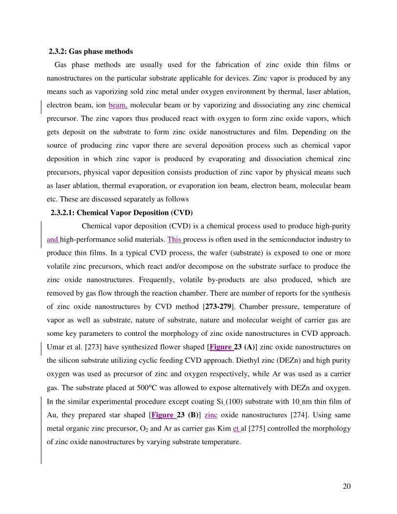
Umar et al. [273] have synthesized flower shaped [Figure 23 (A)] zinc oxide nanostructures on
the silicon substrate utilizing cyclic feeding CVD approach. Diethyl zinc (DEZn) and high purity
oxygen was used as precursor of zinc and oxygen respectively, while Ar was used as a carrier
gas. The substrate placed at 500°C was allowed to expose alternatively with DEZn and oxygen.
In the similar experimental procedure except coating Si (100) substrate with 10 nm thin film of
Au, they prepared star shaped [Figure 23 (B)] zinc oxide nanostructures [274]. Using same
metal organic zinc precursor, O2 and Ar as carrier gas Kim et al [275] controlled the morphology
of zinc oxide nanostructures by varying substrate temperature.
21
2.3.2.2: Physical Vapor Deposition
Physical vapor deposition (PVD) is a variety of vacuum deposition and is a general term
used to describe any of a variety of methods to deposit thin films by the condensation of a
vaporized form of the material onto surface of various substrates. The coating method involves
purely physical processes such as high temperature vacuum evaporation or plasma sputter
bombardment rather than involving a chemical reaction at the surface to be coated as in chemical
vapor deposition. Various PVD methods for the deposition or synthesis of zinc oxide thin films
or nanostructured materials include thermal evaporation or evaporation deposition, electron
beam physical vapor deposition, sputtering (magnetron and RF sputtering), cathodic arc
deposition and pulsed laser deposition etc. These deposition methods for the fabrication of zinc
oxide are discussed in brief as follows.
(a) Evaporative deposition: In which the material to be deposited is heated to a high
vapor pressure by electrically resistive heating in "low" vacuum. Various type of zinc oxide
nanostructures are synthesized by thermal evaporation technique. It is a simple process in which
condensed or powder phase of source material is vaporized at elevating temperature, and then the
resultant vapor phase condenses at certain conditions (temperature, pressure, atmosphere,
substrate, etc.) to form the desired product. There are several processing parameters such as
temperature, pressure, carrier gas (including gas species and its flow rate), substrate and
evaporation time period that can be controlled and need to be selected properly before or during
the thermal evaporation. The source temperature selection mainly depends on volatility of the
source material. Usually, it is slightly lower than the melting point of the source material. The
pressure is determined according to the evaporation rate or vapor pressure of source material.
The substrate temperature usually drops with increasing distance from the position of source
material. The local temperature determines the type of the product to be received. It is also noted
that the thermal evaporation process is very sensitive to the concentration of oxygen in the
growth system. Oxygen influences not only the volatility of the source material and the
stoichiometry of the vapor phase, but also the formation of product. The most common method
to synthesize ZnO nanostructures utilizes a vapor transport process. In such a process, Zn and
oxygen or oxygen mixture vapor are transported and react with each other, forming ZnO
nanostructures. There are several ways to generate Zn and oxygen vapor. Decomposition of ZnO
22
is a direct and simple method, however, it is limited to a very high temperatures (~1200-1400
°C) [280-282]. Another direct method is to heat up Zn powder under oxygen flow [283-285].
This method facilitates relative low growth temperature (500~900 °C), but the ratio between the
Zn vapor pressure and oxygen pressure needs to be carefully controlled in order to obtain desired
ZnO nanostructures. It has been observed that the change of this ratio contributes to a large
variation on the morphology of nanostructures. The indirect methods to provide Zn vapor include
metal-organic vapor phase epitaxy, in which organometallic Zn compound, diethyl-zinc for
example, is used under appropriate oxygen or N2O flow [286]. In the widely used carbothermal
method which is widely used, ZnO powder is mixed with graphite powder as source material
[287]. At about 800-1100 °C, graphite reduces ZnO to form Zn and CO/CO2 vapors. Zn and
CO/CO2 later react and result in ZnO nanocrystals. The advantages of this method lie in that the
existence of graphite significantly lowers the decomposition temperature of ZnO. Synthesis of
zinc oxide nanobelts, nanotapes, nanonails, nanoflowers and various zinc oxide nanostructures
by thermal evaporation method is discussed by us in the reference [272].
(b) Electron beam physical vapor deposition: In which the material to be deposited is
heated to a high vapor pressure by electron bombardment in "high" vacuum of the order of 10-6-
10-9 torr. Polycrystalline zinc oxide pellet or zinc metal are used as target for the electron beam
bombardment and deposition of nanostructured thin film on the substrate. Electron beam energy,
distance between target and substrate, substrate temperature and orientation, order of vacuum are
some key parameters to control the morphology of zinc oxide nanostructures by electron beam
evaporation method. Usually O2 gas at low pressure of the order of 10-5 torr is introduced in the
deposition chamber. Electronic as well as target material collision with O2 ionize it and improve
the crystallinity and stochiometry of zinc oxide thin film. The growth rate of the film is of the
order of 3-5 A°/sec depending on the key parameters used. Asmar et al. [288] have deposited
zinc oxide nanostructured thin film using electron beam evaporation. They employed
polycrystalline zinc oxide target placed in the deposition chamber with 10-6 torr pressure, 5keV
energy of electron beam, 12 cm separation between the target and substrate, Si (100) substrate at
500°C temperature and 8×10⁻⁵ torr oxygen pressure. In another report Qiu et al. [289] have
fabricated well aligned zinc oxide Nanocolumns on Si (100) wafers using electron beam
evaporation. Zinc oxide polycrystalline pellet as target, Si (100) wafer as substrate, ∼3×10⁻³Pa
background pressure of NH3/H2 gas. The diameter and length of the zinc oxide nanocolumns

23
increase with the deposition time [Figure 24]. Giri et al [290] have fabricated nanocrystalline
zinc oxide thin film on alumina silicon and glass substrates at various substrate temperatures
using 6kW electron beam evaporator.
(c) Sputter deposition: In which a glow plasma discharge (usually localized around the
"target" by a magnet) bombards the material sputtering some away as a vapor. Saw el al. [291]
have fabricated zinc oxide thin film of 1µm thickness on saphire (0001) substrate using
sputtering of a pure sintered zinc oxide bulk target in argon atmosphere using a 200 W direct
current magnetron source. After sputtering the film was annealed at 80°C temperature in nitrogen
atmosphere for 2h. Tetrapod like nanostructures of zinc oxide are grown after the annealing of as
synthesized zinc oxide thin film [Figure 25]. Metallic zinc was used as magnetron target for the
fabrication of zinc oxide thin film on the soda lime glass substrate by Kim et al. [292]. Single
crystalline zinc oxide nanobelts are synthesized by Choopun et al. [293] using radio frequency
(RF) sputtering. In a typical experimental procedure, zinc oxide polycrystalline target placed in
the deposition chamber with 1×10⁻⁵ torr vacuum is subjected to 300W of RF power for 60 minute
to deposit zinc oxide thin film on the copper substrate at room temperature. Nanostructured zinc
oxide thin films are grown on p-type Si (100) substrate using RF sputtering by Youn et al. [294].
They have employed 3.8×10⁻³ Pa vacuum, 150W RF power, 50 mm substrate to target distance.
The O2/Ar flow ratio was 0.0, 0.2, and 0.4 and deposition time was 15-50 minute under 2.3Pa
ZnO vapor pressure. Oxygen/Ar ratios in carrier gas and deposition time were used for
controlling the morphology of zinc oxide nanostructured thin films [Figure 26].
(d) Cathodic Arc Deposition or Arc-PVD: It is a physical vapor deposition technique in
which an electric arc is used to vaporize material from a cathode target (zinc for the fabrication
of zinc oxide). The vaporized material then condenses on a substrate, forming a thin film. The
technique can be used to deposit a metallic, ceramic, and composite film. The arc evaporation
process begins with the striking of a high current, low voltage arc on the surface of a cathode
(known as the target) that gives rise to a small (usually few micrometers wide), highly energetic
emitting area known as a cathode spot. The localized temperature at the cathode spot is
extremely high (around 15000 °C), which results in a high velocity (10 km/s) jet of vaporized
cathode material, leaving a crater behind on the cathode surface. The cathode spot is only active
for a short period of time, and then it self-extinguishes and re-ignites in a new area close to the
previous crater. This behavior causes the apparent motion of the arc. Since the arc is basically a

24
current carrying conductor it can be influenced by the application of an electromagnetic field,
which in practice is used to rapidly move the arc over the entire surface of the target, so that the
total surface is eroded over time. The arc has an extremely high power density resulting in a high
level of ionization (30-100%), multiply charged ions, neutral particles, clusters and macro-
particles (droplets). If a reactive gas is introduced during the evaporation process, dissociation,
ionization and excitation can occur during interaction with the ion flux and a compound film will
be deposited. Filtered vacuum cathodic arc deposition (FVAD) of zinc oxide thin film at low
substrate temperature (50-400°C) is employed by magnetically directing vacuum arc produced,
highly ionized and energetic plasma beam onto substrates [295], obtaining high quality coating
at high deposition rates. H. Takikawa et al. [296] have deposited zinc oxide thin film on glass
substrate using steered and shielded reactive vacuum arc deposition. They have used a strong
permanent magnet behind the cathode to drive cathode spot on the cathode surface and employed
30A DC and 0.1 to 5 Pa in process pressure. The rate of deposition increases with pressure upto
1Pa with weak as well as strong magnets. All the deposited thin films had strong ZnO (200)
peak, revealing c-axis orientation [Figure 27]. Aluminum doped zinc oxide thin films were also
deposited by W. Kakikawa et al. [297] using cathodic arc deposition with activated anode
(CADAA). They employed zinc cathodic arc with O2 flow at the pressure of 1 Pa, aluminum
precursor powder as a dopant placed into a crucible acting as anode. The anodic plume plasma
appears on the crucible anode is composed of cathodic material zinc, anode material Al as well
as reactive gas of oxygen.
(e) Pulsed laser ablation deposition: High energy laser is used to vaporize or ablated
depending on laser irradiance zinc/zinc oxide bulk target in O2 or/and inert gas at particular
pressure. Vaporized materials get deposit on seeded/ unseeded, crystalline/ non crystalline
substrate placed perpendicular to the direction of plume flow at particular distance from the
target substrate. Laser irradiance, laser wavelength, pressure inside the chamber, ratio of oxygen
with inert gas, distance of substrate from target, substrate temperature, nature and orientation of
substrate are some key parameters to control morphology of laser produced zinc oxide thin films
or nanostructures. Fabrication of zinc oxide thin films and nanostructured materials uing pulsed
laser deposition (PLD) [298-301], nanoparticle assisted pulsed laser deposition (NAPLD) in gas
chamber [302-305], laser vaporization controlled condensation (LVCC) [306-309] and NAPLD
in quartz tube furnace [310-313] are discussed in detail by us in the ref. [272].
25
2.3.2.3: Spray Pyrolysis Deposition:
Spray pyrolysis is a simple CVD processing technique used to prepare thin and thick
films, ceramic coating and powders. It is simple, relatively cheap, and offers easy technique to
prepare thin film of any composition. It does not require high quality of substrates and chemicals
and is used to produce dense film, porous film and powders. In this technique precursor of the
material to be deposited is in solution and sprayed onto a heated substrate using air as a carrier
gas. Typically spray pyrolysis equipment consist of an atomizer, precursor solution, substrate
heater, and temperature controller. Several types of atomizer such as air blast (liquid is exposed
to a stream of air), ultrasonic atomizer (ultrasonic wave is used for atomic ionization), and
electrostatic (Electric field is used for atomization) are used recent days in spray pyrolysis.
Deposition temperature, precursors solution properties such as precursor, solvent, pH of the
solution and type of atomizer are some key parameters some key parameters to control the
morphology of thin film in spray pyrolysis method. For the fabrication of zinc thin films and
nanostructured materials any zinc precursor can be used. Nanostructured zinc oxide layers
having well shaped hexagonal zinc oxide nanorods were deposited on ITO coated glass sheets
using spray pyrolysis by Krunks et al. [314]. In a typical experimental procedure they utilized
0.02-0.2 mol/lit aqueous solution of zinc chloride as zinc precursor, 400-560°C substrate
temperature, 2.5ml/min spray rate and compressed air as carrier gas for the fabrication of zinc
oxide nanostructured film [Figure 28]. Zinc oxide thin film was prepared by Ashour et al. [315]
by spraying 0.2M aqueous solution of zinc acetate mixed with methanol in the ration of 1:3 with
5ml/min spray rate on a glass substrate at 420°C substrate temperature. Polycrystalline zinc
oxide thin film having wurtzite crystal structure with 20 nm grain size was produced. In a similar
experimental procedure Krunks and Mellikov [316] fabricated zinc oxide nanostructured thin
film utilizing solution of zinc acetate dihydrate in a mixture of 2:3 volume ratios of deionized
water and isopropyl alcohol with addition of some drops of acetic acid to prevent zinc hydroxide
precipitation. The stock solution thus obtained was subjected to spraying on the 475-700°K
heated glass substrate using air as carrier gas. They have reported that the thickness of deposited
zinc oxide thin film decreases with the increase of substrate temperature from 475-700°K, which
may be due to the diminished mass transport to the substrate at higher temperatures. They have
also reported that the growth rate of zinc oxide is unaffected by adding (0-5 at %) InCl3 in the

26
precursor solution for the fabrication of indium doped zinc oxide nanostructured film. Quantana
et al. [317] have studied influence of pH of precursor solution and substrate temperature on the
growth and morphology of nanostructured zinc oxide thin films by spray pyrolysis method and
reported that increasing the deposition temperature increase the particle size until transform it in
round nodules, while change in the shape from planner at low pH to round shape at high pH was
observed.
2.4: Applications of Zinc Oxide nanostructures
Zinc oxide nanostructured material has numerous potential applications in photonics, electronics,
optoelectronics, sensors, energy storing and harvesting device fabrications etc. Zinc oxide has
excellent transparency in the visible, while good absorbance in the UV region therefore, used as
window and sunscreen material. Instead of high transparency it has several other favorable
properties such as high electron mobility, wide bandgap, strong room-temperature luminescence,
etc. These properties are already used in emerging applications for transparent electrodes in
liquid crystal displays and in energy-saving or heat-protecting windows, and electronic
applications of ZnO as thin-film transistor and light-emitting diode. The potential applications of
zinc oxide are discussed under the following sections.
2.4.1: Semiconductor nanolasers
Semiconductor nanostructures have potential application as a lasing material to
produce intense, monochromatic and coherent light sources due to the decrease in threshold
potential for lasing with decrease in size. Efficient stimulated emission and lasing may be
obtained from nanostructures because band edge transfer integral of nanostructures is larger than
the bulk semiconductor. There is no any report on the electrically pumped lasing action in the
zinc oxide nanostructures besides availability of n-ZnO as well as p-ZnO nanostructures, while
optically [195-204] and electron beam [205-207] pumped stimulated emission and lasing have
been reported by several workers in zinc oxide nanostructures including nanorods, nanowires as
well as epitaxial layers synthesized by various routes. As zinc oxide has higher excitonic binding
energy at room temperature as compared to other wide band gap semiconductor, therefore
excitonic emission may also be realized for efficient stimulated emission and lasing. Low
threshold stimulated emission and lasing action may be induced in zinc oxide nanostructures by
exciton - exciton scattering due to its occurrence at a threshold smaller than that require for

27
electron hole plasma recombination. Stimulated emission combined with the excitonic transition
makes zinc oxide nanostructures the most important candidate for the development of UV/blue
semiconductor lasers. Stimulated emission spectra from zinc oxide nanowire array below and
above the lasing threshold are investigated by Huang et al [318]. Opposite facets of zinc oxide
nanorods and nanowires act as two mirrors of laser cavity and zinc oxide acts as active media.
Multiple oscillations between the opposite facets of zinc oxide nanorods, nanowires and thin
films achieve the condition of population inversion for lasing. Optically pumped ordered array of
zinc oxide NRs, NWs grown on any substrates emits monochromatic light in the direction of the
length of rods or wires and the phenomenon is called as ordered lasing. Zinc oxide spherical
nanoparticles or films containing particles, rod or wires have random orientation and condition of
population inversion is achieved by scattering among the surfaces of several nanoparticles. In
this case light is non monochromatic and not unidirectional. There is large number of reports on
the random lasing from zinc oxide nanoneedles [319], 3-D nanostructures [320], and zinc oxide
nanorod array embedded into zinc oxide epilayers [321]. Tanemura et al. have observed random
lasing action in N-doped ZnO nanoneedles [319] and studied pumping power dependent lasing
action [Figure 29]. Gargas et al. [322] have observed lasing from a single zinc oxide nanowire
using scanning confocal microscopy. They have stimulated emission from vertical zinc oxide
cavity using pulsed 266 nm optical excitation at grazing incidence and collected signal using
microscope objective, fiber coupled spectrometer and recorded with CCD [Figure 30].
2.4.2: Light emitting diodes (LEDs)
The attractiveness of zinc oxide LEDs stems from the potential for phosphor-free
spectral coverage from the deep ultraviolet (UV) to the red, coupled with a quantum efficiency
that could approach 90% and a compatibility with high-yield low-cost volume production. These
LEDs have capability to outperform their GaN-based cousins (which offer a narrower spectral
range) due to its three key characteristics such as superior material quality, an effective dopant
and the availability of better alloys. The superior material quality is seen in the low defect
densities of ZnO layers. The p-type dopant has provided hole-conducting layers for ZnO-based
devices and growth of BeZnO layers has shown that it is possible to fabricate ZnO-based high-
quality heterostructures ("The advantages of ZnO over GaN"). ZnO also promises very high
quantum efficiencies, and UV detectors based on this material have produced external quantum
efficiencies (EQE) of 90%, three times that of equivalent GaN-based detectors. The physical

28
processes associated with detection suggest that similarly high efficiency values should be
possible for the conversion of electrical carriers to photons. So it is plausible that ZnO LEDs will
have an EQE upper limit that is three times higher than that of GaN-based devices. There are
three main advantages of zinc oxide based LEDs over that of GaN based as follows
(i) Superior material quality, which has been demonstrated by growth of high purity ZnO
with defect densities below 105cm-2, a value typically associated with the best GaN films.
(ii) Improve doping performance, which results from the arsenic p-type dopant that has
activation energy of 119 meV in ZnO films, which is less than that of 215 meV for
magnesium doped p type GaN. This lower activation energy produces a ten fold increase
in the proportion of the activated accepter atoms that are needed for electrical conduction
and also reduces the number of defects for a given hole carrier density.
(iii) The availability of better alloys, due to our recent development of high quality BeZnO
films. These layers have driven the fabrication of LEDs, lasers and transistors that have
less disorder than the structure produced using the AlGaN/GaN material system. The
reduced disorder is a consequence of the large difference in band gap between ZnO and
BeO and enables only small changes in the alloy’s composition to produce relatively
large changes in band gap. In comparison, a much larger shift in aluminum composition
is required.
Wang et al. [53] have fabricated zinc oxide hetrojunction LEDs with plasma enhanced chemical
vapor deposited (PECVD) SiO2 and SiNx . They have investigated passivation effects of PECVD
SiO2 and SiNx on ZnO based p-i-n LEDs. The LED structure consisted 450 nm Ga:ZnO on
sapphire, 40 nm of Zn0.9Mg0.1O, 40 nm i-ZnO, 40 nm of Zn0.9Mg0.1O and 40 nm of phosphor p
doped ZnO as shown [Figure 31]. Kim et al. have used p-type zinc oxide as a hole injection
layer to enhance the output power of GaN LED [54]. A topical review by Willander et al. on zinc
oxide based LEDs illustrates recent advances of zinc oxide based LEDs on crystalline as well as
amorphous substrates [55]. Willander et al. have grown n type zinc oxide nanorods using
different approaches on the p type SiC and observed expected electroluminescence from them
[56]. They have measured and analyzed I-V curve in order to insure that the fabricated LED
behavior is the consequence of p-n junction between n type ZnO and p-type SiC epilayer. The
fabrication of n-ZnO nanorods on p-SiC LEDs by VLS approach illustrated visible emission at

29
almost 30 V [Figure 32], which shows strong white light emission with color rendering index
92, higher than that of commercially available white light LEDs [56]. They used CVD grown p-
type epitaxial thin layer on n-type SiC epitaxial layer as a substrate to grow n-ZnO ordered
nanorods to fabricate n-ZnO/p-SiC hetrojunction LED to operate at lower operating potential
(18V) compared to that mentioned earlier (30V) [56]. Epitaxial zinc oxide thin films or
nanostructures grown on GaN crystalline substrates have potential application as LEDs or
nanolasers due to the very small lattice mismatch (only 2 %), which insures a lower defect
density in zinc oxide nanostructures on GaN substrate as compared to others. In spite of these
they have same fundamental band gap of 3.4 eV and same wurtzite crystal structure. There are
several reports on the growth of zinc oxide nanostructures on GaN crystalline substrates and their
LED demonstrations [57-59]. All of these reports on ZnO nanorods/GaN substrate LEDs exhibit
enhanced EL emission and improved injection current as compared to the conventional ZnO thin
film/GaN substrate LEDs due to the reduced interfacial defects from nanosized junctions.
Fabrication of n-ZnO/p-Si LEDs are also reported besides indirect and large bandgap difference
of Si from zinc oxide. Zinc oxide thin films [60] as well as nanorods [61, 62] are grown on Si
substrates and demonstrated for visible hetrojunction n-ZnO/p-Si LEDs. It is the property of
zinc oxide NRs or NWs that it can be also easily grown on any type of substrates such as glass,
polymers, plastics, and metal oxide bulk surfaces. For LED applications zinc oxide
nanostructures are usually grown on ITO or FTO coated glass substrates due to their transparent
and conducting nature. The fabrication of n-zinc oxide nanostructures as n-electrode on the p-
type organic semiconductor substrate as p-electrode called as hybrid inorganic/organic LEDs
and have potential for industrialization due to the numerous advantages including possibility to
fabricate UV to red LEDs varying the type and nature of p-type substrate, combination of UV
and green emission from zinc oxide excitonic and defect level, respectively with the emission
from the hybrid structure makes the white light of better CI values. Large numbers of reports on
zinc oxide nanostructures on organic substrates to fabricated hybrid LEDs are available in
literatures [62,63]. Zinc oxide/polymer nanocompites are synthesized for the fabrication of
inorganic-organic hybrid white light LEDs separately by Zhang el al. [63] and Uthirakumar et al.
[64]. Inorganic zinc oxide nanorods are grown on the organic PEDOT: PSS [poly (3,4-
ethylenedioxythiophene) poly(styrenesulfonate)] on glass substrates with some other organic
hole injection layer for the fabrication of inorganic/organic hetrostructure LEDs by Willander et

30
al.[55]. Two layers of PEDOT:PSS were deposited by them on glass substrate as bottom contact
layer, followed by deposition of hole transport and polymer emitting layer [Figure 33]. On the
surface of polymer emitting layer zinc oxide nanorods are grown as electron transport and light
emitting layer. Gold was deposited on the top of zinc oxide nanorods as top contact layer. For
hole transport and polymer emitting layer they have selected two different combinations NPD [4-
4’-bis[N-(1-naphthyl)-N- phenyl-amino] biphenyl] and PFO [Poly (9,9-dioctylfuorene)] for the
first case [Figure 34 a] and TFB [poly(9,9-dioctyl-fuorene-co-N(4- butylphenyl)diphenylamine]
with PVK [poly(N-vinylcarbazol] as the later case [Figure 34 b]. In the first case PFO was
added with the NPD in multilayered configuration, while PVK was blended with TFB for the
second case. NPD enhances the hole transport divides the hole energy barrier into two separate
barriers to increase the probability of exciton recombination. Similarly TFB enhances the hole
transport, provide a wider emission range, and acts as an electron blocker. It also increases the
viscosity of blended solution, and hence improves quality of film. They have reported turn on
and breakdown voltages for first device are 4V and -15V respectively, while these are 3V
and -6 V for second device. Rectification factor for the first device is 10, while it is only 3
for the second device. Low turn on voltage of second device as compared to first is due to
less number of layers hence less series resistance.
2.4.3: Solar Cells and light detectors
Research and development in the direction of renewable energy sources are highly
demanded due to the limited availability and pollution creating nature of conventional fossil
fuels. Investigations in the fabrication of new and improvement in the existing solar cells is a
most effective effort in this direction. Solar cells are p-n junction diodes in which photocarriers
are generated by sunlight at the p-n junction and are migrated through the external circuit before
the recombination. A material having efficient photocarrier generation efficiency, high charge
mobility, low electron/hole trapping level is required to fabricate efficient solar cells. Crystalline
silicon solar cell with 20% practical efficiency is one of the photovoltaic cells and currently
occupies 94% of the market, but it is too costly to commercialize. Therefore, other options of
cheap fabrication of efficient solar cells are developed. One of the options is excitonic solar cells
having metal oxide thin films or nanostructures (Film of nanoparticles or other nanostructures,
array of NRs, nanotubes on substrates) with dye molecules, or organic molecules/polymers, or

31
semiconductor quantum dots as photoanode and a counter metallic photocathode. Dye or organic
molecule/polymers or quantum dots acts as sensitizer, absorbs most of the portion of solar
radiation and generates photocarriers. Depending on the type of sensitizer there are three types of
semiconductor solar cells (a) with dye as sensitizer called Dye Sensitized Solar Cells (DSCs) (b)
with polymer/organic molecule called Hybrid Solar Cells (HSCs) and with quantum dots as
sensitizer called Quantum Dot Solar Cells (QSCs).
(a) Zinc oxide based Dye Sensitized Solar Cells (DSCs)
DSCs based on oxide semiconductor film or nanostructures and organic or metal- organic
complex dyes open an emerging area of fabrication of cost effective and efficient photovoltaic
solar cells. The DScs are the photoelectrochemical systems having porous metal oxide
semiconductor thin film or nanostructures with adsorbed dyes as photoanode, a platinized
fluorine or indium doped tin oxide as a counter electrode, and a liquid electrolyte usually contain
I-/I3- redox couple to electrically connect the two electrodes. Monolayer of the dye molecule
absorbs photon and creates excitons, which rapidly get split at the surface of metal oxide
nanostructures. Electrons are injected through the metal oxide nanostructures, while the holes are
released by redox couples in the electrolyte. Titanium dioxide thin film is most efficient DSCs
with 10.4% conversion efficiency [15-18], due to the porous nature of titanium dioxide thin film
(Provide larger surface area for the loading of dye molecules) and lower energy of its conduction
band edge as compared to the LUMO of the dye molecule. But conversion efficiency of titanium
dioxide based DSCs are limited due to the absence of depletion layer on its surface, which causes
carrier loss due to the recombination process. As zinc oxide is wide band gap semiconductor and
have physical and electronic band structure same as that of the titanium dioxide with higher
electron mobility, therefore reduces photo carrier loss due to recombination when used in DSCs.
Instead of these properties zinc oxide can be easily grown in various anisotropic nanostructures
on cheap substrates with low electron trap level, which makes it suitable for the future alternative
of costly Si based solar cells. Not only the large surface area, higher carrier mobility and good
crystallinity is required for fabrication of efficient solar cells but also geometry such as
orientation and morphology are equally important, which determines how long sunlight falls on
the photo-sensitizer loaded on the nanostructured surface. Therefore, DSCs fabricated using
various zinc oxide nanostructures such as ordered and disordered nanorods, nanotetrapods,
nanowires, nanoflowers, spherical nanoparticles and other nanostructures have different light

32
conversion efficiency. A recent review summarizes light conversion efficiencies of DSCs
fabricated from various zinc oxide nanostructures and thin films grown by different methods
[19]. Gao et al. [20] have fabricated DSCs from the solution derived zinc oxide nanowire array
films and studied effect of aspect ratio of nanowires on the conversion efficiency. Zinc oxide
double layer structured film with mono-dispersed aggregates as under layer and submicron
sized platelike structure as upper layer was used for DSC fabrication by Zeng et al. [22] and
reported that the 3.44% efficiency for double layer zinc oxide DSCs, which is 47 % higher
compared to single monodispersed aggregate and far larger than that obtained by micron sized
platelike structures (only 0.81%) alone. Umar [23] has fabricated DSCs from thermal
evaporation synthesized zinc oxide nanocomb like structure grown directly on the FTO
substrates and reported 0.68% conversion efficiency (η), 34% fill factor (FF), 3.14mA/cm2 short
circuit current (ISC) and 0.671V open circuit voltage (VOC). It is also reported by Niinobe et al.
[24] that VOC of tin oxide DSCs enhances by the addition of zinc oxide nanostructures.
Comparative studies between DSCs fabricated from MOCVD grown zinc oxide nanorods (NRs)
array and a mesoporous film of the same thickness prepared from zinc oxide colloids was done
by Galopinni et al. [26] and reported that electron transport in ZnO NRs is two times faster than
that of the zinc oxide colloids, which suggest that morphology of zinc oxide used in the
fabrication of working electrode plays an important role in the electron transport properties and
hence conversion efficiency. Tornow and Schwarzburg [26] transient electrical response of
zinc oxide NRs DSCs and reported intrinsic resistance and capacitance of as synthesized and
annealed zinc oxide nanorods of different length used in the DSCs. Effect of dye loading
conditions on the η value of DSCs fabricated from zinc oxide film as photoanode is investigated
by Chou and coworkers and reported that higher and lower dye concentration requires a shorter
and longer immersion time, respectively for the optimal sensitization of zinc oxide to obtain
maximum sensitization. ZnO/Al2O3 and ZnO/TiO2 core/shell NRs were used for the fabrication
of DSCs by Law and coworkers [27]. They used atomic layer deposition (ALD) of amorphous
Al2O3 or anatase TiO2 on the surface of zinc oxide NRs and reported that alumina shells of all
the thickness act as insulating barriers between the NRs and enhance VOC with large decrease in
the ISC, while titania shells of 10-25 nm thickness cause high increase in the VOC and fill factor
with slight fall in the ISC. Effect of doping of zinc oxide nanorods of different sizes in the TiO2
photoanode on the performance of DSCs is investigated by Pang et al. [28]. They have reported

33
that conversion efficiency enhances 15% with the addition of 1w% zinc oxide, while carrier
diffusion rate increases 1-3 orders of magnitude depending on size of NRs and suggested that
addition of ZnO NRs enhances charge carrier transport, decreases rate of recombination,
improved VOC value and hence improve in the overall conversion efficiency. DSC fabricated
with branched zinc oxide NRs shows twice conversion efficiency as compared to bare ones.
(b) Zinc oxide based Hybrid Solar Cells (HSCs)
Organic –inorganic hybrid solar cells have ability to provide cheap, flexible, smaller and
thinner photovoltaic devices in large scale. As most of the organic molecules and polymers are
soluble in the organic solvent and can be easily coated on the surface of semiconductor film or
nanostructures by any one of the solution processing such as spin coating, roll by roll
technology, inkjet printing, screen printing and spray methods. As most of the polymers have
high absorption coefficient (105cm-1), short exciton length due to the less than 10 nm diffusion
length and very low hole mobility (10-1-10-7 cm2V-1 s-1) as compared to silicon (500 cm2V-1 s-),
therefore several parameters have to be optimize to get good conversion efficiency. The HSCs
are not as more advanced as DSCs due to their low conversion efficiencies, however, it is
beneficial due to the cheapest and easiest fabrication of excitonic solar cells. Single crystalline
zinc oxide NRs/NWs array are used in the HSCs to speed electron conduction and hence
improving conversion efficiency. Single crystalline zinc oxide NWs having 30-100 nm dia. and
micron sized lengths on quartz substrate obtained by solution and vapor phase methods are used
for the fabrication of ZnO/ poly(3-hexylthiophene) (P3HT) and ZnO/ didodecylquaterthiophene
(QT) hybrid solar cells [29]. Incorporation of lithium ions during the sol-gel processing of metal
oxide layer is done by Lloyd and coworkers to enhance conversion efficiency of ZnO/P3HT
HSCs by a factor of 2.9 [30]. They have reported enhancement in the VOC and ISC upto an
optimum Li concentration between 15 and 20 atomic percentage. Olson et al. [31] have studied
effect of zinc oxide processing conditions i.e morphology on the photovoltage of ZnO/P3HT
HSCs and reported that ZnO film/NRs annealed in air at 150°C temperatures granted ∼ 200mV
VOC, which was higher than that in which ZnO was treated with UV/ozone. ZnO-TiO2 core-
shell/P3HT HSC was fabricated by Greene et al [32], they reported that the atomic layer
deposited TiO2 thin shell on zinc oxide surface enhances voltage and fill factor relative to that
without shell and performance of the cell increases with its exposure to air. An elaborative work
on HSCs having crystalline zinc oxide nanoparticles (nc-ZnO) as electron acceptor and blends of

34
conjugated polymer poly[2-methoxy-5-(3’-7’-dimethyloctyloxy)-1,4-phenylenevinylene]
(MDMO-PPV) as electron donor has been done by Beek et al. [33] and reported that a
photoinduced electron transfer from MDMO-PPV to nc-ZnO occurs in these blends on a sub
picosecond time scale and produces a long lived charge separated state. They have investigated
conversion efficiency as a function of zinc oxide concentration and thickness of the layer, size,
shape and surface modification of zinc oxide and degree and type of mixing of the two
components.
(b) Zinc oxide based Quantum Dot Sensitized Solar Cells (QDSSCs)
In this case semiconductors or metallic quantum dots (QDs) are used as photo-sensitizer
to create photoelectron and metal oxide thin films or NRs/NWs arrays are used as electron
acceptor. Due to the size dependent tunable optical and electronic properties of semiconductor
QDs, they can have potential ability to enhance efficiency of excitonic solar cells. Choosing
suitable semiconductor QDs of particular size in such a way that its conduction band lies above
the conduction band of zinc oxide NRs/NWs or thin films or other nanostructures used as
electron acceptor in QSCs. An array of vertically grown zinc oxide nanowires on the conducting
FTO substrate along with mercaptopropionic acid capped CdSe QDs as sensitizer was used for
the fabrication of QDSC by Leschkies and coworkers [34]. QDs when illuminated with light
eject electrons across the quantum dot nanowire interface, which are transported to the
photoanode through the path provided by the morphology of zinc oxide nanorods, while the
liquid electrolyte provide the path for the transportation of holes to the counter electrode. Lead
selenide quantum dot was used as photosensitizer with zinc oxide thin film to fabricated zinc
oxide based QDSSCs with higher conversion efficiency as compared to the Schottky diode made
of the similar zinc oxide film [34]. Other reports for the application of zinc oxide nanorods, thin
films in the fabrication of QDSSCs excitonic solar cells are also available [35-37].
The working principle of solar cells is similar to that of the light detector. Both require
high number excitons generated by single photon on the p-n junction, their dissociation into
electron and holes at the interface and transportation of charge carriers towards the electrodes
with minimum number of recombination to fabricate efficient solar cells and photo detector. As
zinc oxide is wide band gap semiconductor, absorbs UV light, high exciton binding energy and
higher carrier mobility therefore it is widely used for the fabrication of zinc oxide based UV
detector. According to Maxtronics Inc., which is fabricating zinc oxide based optoelectronic
35
devices such as solar cells, LEDs and light detector, detector fabricated by zinc oxide
nanostructures are three times more efficient compared to any other solid state detector [143].
Tuning the zinc oxide bandgap by variation in its size or by doping it with various atoms, zinc
oxide photodetectors for UV as well as visible range of high efficiencies and fast response are
fabricated [144-148].
2.4.4: Electronic device fabrication
Electronic devices such as transistors and FETs are fabricated from zinc oxide single
nanorod or nanowire, thin films, as well as using its assembly. Zinc oxide transparent thin film
transistors are very recent development in this area [42]. Doping of zinc oxide with various
atoms can easily change its electronic properties such as carrier concentrations and mobility for
the fabrication of efficient transistors and FETs. Using of organic molecules and/or polymers
with zinc oxide has also potential for the fabrication of hybrid electronic devices [43]. Self
assembly of colloidal zinc oxide nanorods are used for the fabrication thin film field effect
transistor [44]. Fei et al. have fabricated external force triggered FET based on a free standing
piezoelectric zinc oxide wire utilizing Ag and Au source and drain electrodes at the end of the
zinc oxide nanowire channel [45]. Some other but not all reports on the fabrication of zinc oxide
transistors/FETs are given in the literatures [46-48].
2.4.5: Hydrogen generation and storage
Hydrogen is an efficient source of renewable energy and has potential for cheap
replacement of the fossil fuels. Water is the cheapest source of hydrogen and can be break into
its molecular constituents by photolysis. Zinc oxide nanostructures can be used for the
electrochemical photolysis of water. More recently, Deborah V. César et al have observed that
ZnO/TiO2 is a promising system for H2 production [142]. ZnO with TiO2 has also been observed
to be a good composite for producing hydrogen by partial oxidation of methanol [143]. Zinc
oxide also stores hydrogen by its absorption/adsorption. Recent studies reveal that ZnO
nanostructures can able to reversibly absorbs/desorbs hydrogen at ambient temperature and
pressure [146, 147]. Wan et al [146] have first time reported that ZnO nanowires absorbs 0.83
wt% H2 at room temperature and ~30 atm hydrogen pressure. However, it is observed that only
~0.6 wt % (71 %) of the stored hydrogen has been released during desorption. H. Pan et al [145]
have investigated the difference in hydrogen storage characteristics of ZnO nanowires with Mg
doping. Mg doping in place of Zn does not change the wurzite structure of ZnO. However, the

36
maximum hydrogen uptake in Mg doped ZnO nanowire and undoped ZnO nanowire were found
to be 2.8 wt% and 2.57 wt%, respectively. Under ambient conditions these materials show faster
hydrogen uptake and release kinetics.
2.4.6: Sensors
Zinc oxide nanomaterials sensor is an electronic device, which can detect any change
such as temperature, pressure, humidity etc. or presence of any gas or liquid molecule in its
ambient atmosphere. Any change in environmental conditions or presence of any
atoms/molecules highly affects electronic, optical and vibrational properties of zinc oxide, which
can be measured with calibrated devices. The simplest and thus most popular way is to pass
electrical current through the zinc oxide nanorods and observe its changes upon gas exposure.
All types of sensors such as gas [117-120], temperature [121], pressure [122], humidity [123-
127], chemical [128,129], molecules in the solution (glucose, urea etc) are fabricated from zinc
oxide nanostructures [130-135]. As zinc oxide nanowires are ultra sensitive to the tiny forces in
the range of nano to pico newton. Electrical charges get accumulated on the nanowire surface
and decrease the current flowing through it when such a small forces try to deform it. This
phenomenon is utilized to fabricate small pressure sensors, which can measure blood flow rate
and generated pressure in the veins [122]. Zinc oxide based biological sensors to detect urea
[130-132], glucose [133-135], and other biomolecules are available. One cannot imagine that
sequences of bases in the DNA can also be detected using zinc oxide NR based sensor [136],
which is an important step to detect the presence of biothreat agents.
2.4.7: Water and Air Purification
Researchers at Oklahoma State University, US, have used nanoparticles of zinc oxide
to remove arsenic from water, even though bulk zinc oxide cannot absorb arsenic. They
produced the zinc oxide in a porous aggregate form that was suitable for water treatment. Zinc
oxide nanostructures have the property to adsorb most of the toxic gases such as CO2, CO , NO
etc. on its surface, hence are being used as air purifier. It also adsorbs organic molecules such as
dyes [323, 324], alcohol and other industrial chemical from waste water on its surface and photo
catalytically [323, 324] degrade these to purify the water. Therefore, zinc oxide nanostructures
have tremendous applications in the water filter and waste water treatment.

37
2.4.8: Biological and medical Application
Zinc oxide nanostructures have wide range of biological and medical applications due to
its high level of bio and haemo-compatibility. Zinc oxide based pressure sensors can measure
pressure inside a single blood veins, while nano-generator fabricated from these nanostructures
can power heart pacemakers. It has potential to replace conventional dyes and toxic quantum
dots in biomedical applications owing its high photo-stability and low toxicity. Zinc oxide has
found use in a wide range of medical and cosmetic applications. Mixture of Zinc oxide alongwith
about 0.5% Fe2O3 known as calamine is used in calamine lotion. There are also two minerals,
zincite and hemimorphite, which are also known as calamine when mixed with eugenol, the
mixture is called zinc oxide eugenol and has restorative and prosthodontic applications in
dentistry. Zinc peroxide, ZnO2 .½ H2O, is a white to yellow powder that is used in antiseptic
ointments. Its ability to absorb ultraviolet light makes zinc oxide an active ingredient of choice in
suntan lotions. Zinc oxide is well known for its ability to neutralize acid and for its mild
bactericidal properties, making it an ideal component in body cream/antiseptic healing cream to
help reduce soreness and redness. It is also used in medical tapes and plasters, some toothpaste
formulations and in dental cements. And, last but not least, zinc oxide is incorporated in dietary
supplements and vitamin tablets as source of the essential micronutrient zinc for the human
body.
2.4.9: Other Applications:
In addition to above mentioned potential applications of zinc oxide, it has also several
industrial applications. Due to its high refractive index, high thermal conductivity, binding,
antibacterial and UV-protection properties, it is added into various materials and products,
including plastics, ceramics, glass, cement, rubber, lubricants, paints, ointments, adhesive,
sealants, pigments, foods, batteries, ferrites, fire retardants, etc. Its industrial applications are
given as follows
(a) Rubber Industry
About 50% of the total production of ZnO is used in rubber industry. Zinc oxide
along with stearic acid activates vulcanization, which otherwise may not occur at all. Zinc oxide
and stearic acid are ingredients in the commercial manufacture of rubber goods. A mixture of
these two compounds allows a quicker and more controllable rubber cure. ZnO is also an

38
important additive to the rubber of car tyres. Vulcanization catalysts are derived from zinc oxide,
and it considerably improves the thermal conductivity, which is crucial to dissipate the heat
produced by the deformation when the tyre rolls. ZnO additive also protect rubber from fungi
and UV light.
(b) Concrete industry
Zinc oxide is widely used for concrete manufacturing. Addition of ZnO improves the
processing time and the resistance of concrete against water.
(c) Cigarette filters
Zinc oxide is a constituent of cigarette filters for removal of selected components
from tobacco smoke. A filter consisting of charcoal impregnated with zinc oxide and iron oxide
removes significant amounts of HCN and H2S from tobacco smoke without affecting its flavor.
(d) Food additive
Zinc oxide is added to many food products, e.g., breakfast cereals, as a source of zinc,
a necessary nutrient. Some prepackaged foods also include trace amounts of ZnO even if it is not
intended as a nutrient.
(e) Pigment
Zinc white is used as a pigment in paints and is more opaque than lithopone, but less
opaque than titanium dioxide. It is also used in coatings for paper. Chinese white is a special
grade of zinc white used in artists' pigments. Because it absorbs both UVA (320-400 nm) and
UVB (280-320 nm) rays of ultraviolet light, zinc oxide can be used in ointments, creams, and
lotions to protect against sunburn and other damage to the skin caused by ultraviolet lights. It is
the broadest spectrum UVA and UVB absorber that is approved for use as a sunscreen by the
FDA, and is completely photostable. It is also a main ingredient of mineral makeup.
(f) Coatings
Paints containing zinc oxide powder have long been utilized as anticorrosive coatings
for various metals. They are especially effective for galvanised Iron. The latter is difficult to
protect because its reactivity with organic coatings leads to brittleness and lack of adhesion. Zinc
oxide paints however, retain their flexibility and adherence on such surfaces for many years. As
ZnO highly n-type doped with Al, Ga or In is transparent and conductive (transparency ~90%,
lowest resistivity ~10−4 Ωcm ). ZnO:Al coatings are being used for energy-saving or heat-
protecting windows. The coating lets the visible part of the spectrum in but either reflects the

39
infrared (IR) radiation back into the room (energy saving) or does not let the IR radiation into the
room (heat protection), depending on which side of the window has the coating. Various plastics,
such as poly(ethylene-naphthalate) (PEN), can be protected by applying zinc oxide coating. The
coating reduces the diffusion of oxygen with PEN. Zinc oxide layers can also be used on
polycarbonate (PC) in outdoor applications. The coating protects PC form solar radiation and
decreases the oxidation rate and photo-yellowing of PC .
2.5: Summary
Zinc oxide is one of the best semiconductors materials with advanced technological applications
in the fabrication of semiconductor laser diodes, light emitting diodes, transistors/FETs, Solar
cells for energy harvesting, Lithium ion and fuel cells for energy storage, sensors (Physical,
biological as well as chemical), hydrogen generation and its storage, environmental pollution
monitoring and biological/medical applications. It provides material for laser diodes with broad
spectral coverage from deep UV to near IR, white as well as colored LEDs. As the highest
conversion efficiency of zinc oxide based DSCs have reached upto 4-5% yet, which is too lower
than that based on the titanium dioxide base DSCs, but it is expected that zinc oxide may be used
to replace Si based costly solar cells with high efficiency. ZnO has also been considered for
spintronics applications if it is doped with 1-10% of magnetic ions (Mn, Fe, Co, V, etc.) and
becomes ferromagnetic, even at room temperature. The piezoelectricity in textile fibers coated
with ZnO has been shown capable of fabricating "self-powered nanosystems" with everyday
mechanical stress from wind or body movements. Instead of technological and biological
applications it has also tremendous industrial applications. There is large number of cheap and
simple available physical and chemical, solution and vapor phase routes for the synthesis of wide
morphology of zinc oxide nanostructures with great optoelectronic, electronic, spintronic and
optical properties, which makes it more popular amongst the researchers.
3: Cuprous Oxide (Cu2O) Nanostructures; Synthesis, Characterizations and applications
3.1 Introduction
Synthesis of inorganic nanostructures with reliable low cost and well defined morphology
have attracted considerable attentions for the dimensional and structural characteristics of these

40
materials endowed with wide range of potential applications in electronic magnetic and photonic
devices. The unique properties of semiconductor and metal oxides could be harnessed for the
design and fabrication of nanosensors [325], switches [326], nanolasers [327] and transistors
[328]. Among different metal oxide materials copper based nanomaterials (nanowires and
nanobelts etc) are of great interest because of their applications as inter connectors for
microelectronics. Copper containing complexes are indispensable in biological processes for
their ability to act as oxygen carriers in oxidation reactions [329], in reactions involving DNA
hydroxocomplexes [330] and in biological enzymes such astyrosinase [331] and oxyhemocyanin
[332].
3.2 Crystal structures and Physical Properties of Cuprous Oxide
The physical properties of the cuprous oxide (Cu2O) are given in the table 2. Copper (I)
oxide or Cu2O is an oxide of copper and belongs to the BCC Cubic crystal system with lattice
parameters a = 0.4269 nm. It is insoluble in water and organic solvents. Copper(I) oxide
dissolves in concentrated ammonia solution to form the colorless complex [Cu(NH3)2]+, which
easily oxidizes in air to the blue [Cu(NH3)4(H2O)2]2+. It dissolves in hydrochloric acid to form
HCuCl2 (a complex of CuCl), while dilute sulfuric acid and nitric acid produce copper(II) sulfate
and copper(II) nitrate, respectively. Copper(I) oxide is found as the mineral cuprite in some red-
colored rocks. When it is exposed to oxygen, copper will naturally oxidize to copper (I) oxide,
but this takes extensive time. Artificial formation is usually accomplished at high temperature or
at high oxygen pressure. With further heating, copper(I) oxide will form copper(II) oxide.
Formation of copper(I) oxide is the basis of the Fehling's test and Benedict's test for reducing
sugars which reduce an alkaline solution of a copper(II) salt and give a precipitate of Cu2O.
Cuprous oxide forms on silver-plated copper parts exposed to moisture when the silver layer is
porous or damaged; this kind of corrosion is known as red plague.
3.3 Synthesis of Cu2O Nanostructures
The Cu2O nanostructures have been prepared by several different methods such as
electrodeposition, sonochemical method, thermal relaxation, liquid phase reduction, complex
precursor surfactant-assisted (CPSA) route and vacuum evaporation. Basically these methods
can be divided in to two methods ie template based methods and template free methods. Various
approaches for the synthesis of different nanostructures have been discussed below in detail.

41
3.3.1: Synthesis of Cu2O nanostructures by electrodeposition
Well-defined, polycrystalline Cu2O was electrodeposited on TFO conducting substrates
by de P. E. Jongh et al [333]. The temperature of the deposition solution, ranging from 10 to 65
°C, had a strong influence on the morphology of the oxide and on the deposition kinetics (Figure
35). At and below room temperature, a steady decrease in potential occurred during the
deposition, limiting the thickness of the layers. Larger crystals were grown at higher
temperatures. The pH of the solution strongly influenced the nucleation process and the
morphology of the layers. The as-deposited Cu2O was stable under ambient conditions.
Cuprite (Cu2O) nanowires with diameter of 25-100 nm were electrodeposited from
anionic surfactant sodium bis(2-ethylhexyl) sulfosuccinate reverse hexagonal liquid crystalline
phase by L. N. Huang et al [334]. They showed that Cu2O nanowires with high aspect ratio can
be readily electrodeposited from lyotropic reverse hexagonal liquid crystalline phases.
Hexagonal liquid crystal phase with improved alignment played an important role in the
formation of the nanowires. The nanowires were grown up to tens of micrometers in length by
simply changing the electrodeposition time. Resistivity measurements suggested improved
alignment of the reverse hexagonal liquid crystalline phase under electric field during
electrodeposition. The enhanced alignment of the liquid crystalline phase was essential for the
growth of nanowires with high aspect ratio. R. Liu et al. [335] deposited epitaxial bulk Cu2O
films onto InP(001) with tunable morphologies and epitaxial chiral CuO films onto Au single
crystals. They electrodeposited the epitaxial Cu2O nanocrystals onto InP(001). The growth
kinetics was controlled by the pH of the deposition solution and led to a pyramidal morphology
at pH 9 and a cubelike morphology at pH 12.
Cylindrical microstructures of Cu/Cu2O were electrochemically produced by S. Leopold
et al. [336] from the self-oscillating Cu(II)-lactate system using etched ion track polycarbonate
membranes as templates. After removal of the polymer, arrays of free-standing cylinders were
obtained. The influence of the applied current density and the deposition temperature on the
oscillation pattern and quality of the deposited wires were studied for pores having a diameter of
about 1000 nm. The widest current density range for oscillations was found at 25 0C. Under these
conditions the deposited wires were of equal length and showed smooth contours, while a
granular structure was observed at higher temperatures. Potentiostatic deposition of Cu2O

42
nanowires (Figure 36) in polycarbonate membrane by cathodic reduction of alkaline cupric
lactate solution was studied by A. L. Daltin et al. [337]. Pure cuprous oxide nanowires were
obtained by the potentiostatic technique even if high current intensities were reached in the first
moments of the deposition process. The Cu2O nanowires had uniform dimension of
approximately 100 nm and lengths up to 16µm.
Template-mediated electroplating was used to fabricate Cu2O nanorod arrays by Y. H.
Lee. et al [338]. A morphological study showed that the nanorods of 60 nm diameter and 450 nm
in length were perpendicular to the substrate. Cu2O nanowires, mainly consisting of (100) and
(200) with a length of 4 µm were prepared by electrochemical deposition using a porous alumina
template by K. Eunseong et al. [339]. The optimized electrochemical conditions to prepare
Cu2O nanowires were different from those for the formation of a bulk thin Cu2O layer since
different pH values were found between the tip of the pores and the bulk.
K. E. R. Brown et al [340] demonstrated a facile electrochemical procedure that can
produce highly transparent Cu2O films using a DMSO medium. The resulting films were
composed of ~ 10 nm sized nanocrystals. S. Guo et al [341] reported a electrochemical route for
the controlled synthesis of a Cu2O microcrystal from perfect octahedra to monodisperse colloid
spheres via control of the electrodeposition potential without the introduction of any template or
surfactant. Perfect Cu2O octahedra and monodisperse colloid spheres were obtained in high yield
(~100%) (Figure 37). The size of octahedral Cu2O were easily controlled via simple control of
the deposition time, the electrodeposition potential, and the concentration of Cu(OH)42-. The
morphology of Cu2O was changed to monodisperse colloid spheres when the electrodeposition
potential was changed to -0.7 V.
3.3.2: Synthesis of Cu2O nanostructures by anodic Oxidation
D. P. Singh et al. [342] synthesized different cuprous oxide (Cu2O) nanostructures
(Figure 39) by anodic oxidation of copper through a simple electrolysis process employing plain
water (with ionic conductivity~6µS/m) as an electrolyte. No special electrolytes, chemicals, and
surfactants were used. Platinum was taken as cathode and copper as anode. The applied voltage
was varied from 2 to10 V. The optimum anodization time of about 1 h was employed for each
case. Two different types of Cu2O nanostructures were formed. One type was delaminated from
copper anode and collected from the bottom of the electrochemical cell and the other was located

43
on the copper anode itself. The nanostructures collected from the bottom of the cell were either
nanothreads embodying beads of different lengths and diameter ~10-40 nm or nanowires (length
~600-1000 nm and diameter ~10-25 nm). Those present on the copper anode were nanoblocks
(Figure 39) with a preponderance of nanocubes (nanocube edge ~400 nm). The copper electrode
served as a sacrificial anode for the synthesis of different nanostructures. Both anodization
potential and time influenced the morphology of nanostructures of Cu2O. Nanothreads were
formed at 6 V during 15-30 min, whereas nanowires resulted when anodization time was
extended to 45-60 min.
J. Gao et al [343] synthesized uniform hollow spheres of Cu2O and CuS by chemical
transformation of in situ formed sacrificial templates containing Cu(I) in aqueous solutions. The
shell thickness of these hollow spheres were adjusted through the choice of the bromide source
used for the formation of intermediate templates. Specifically, thick-shell hollow spheres (about
130-180 nm in shell thickness) were obtained by using CuBr solid spheres as the templates,
which were formed by the reduction of CuBr2 with ascorbic acid; on the other hand, thin-shell
hollow spheres (about 20-25 nm in shell thickness) were obtained by using spherical aggregates
consisting of the Cu+, Br-, and (C4H9)4N+ ions as the templates, which were formed by the
reduction of CuCl2 with ascorbic acid in the presence of (C4H9)4NBr. Figure 40 a and b show the
SEM and TEM images of the thick shell hollow Cu2O nanostructure after reaction with NaOH
and CuBr solid spheres. Uniform Cu2O hollow spheres (Figure 40 c and d) with a diameter of
about 510 nm were obtained when NaOH was added to the reaction solution at room
temperature.
Nanowires of Cu2O as well as Cu were synthesized by H. S. Shin et al. [344] within the
anodic aluminum oxide templates in an aqueous acidic electrochemical cell. The content of Cu2O
in the copper nanowires was controlled by varying the anodic potential of the pulse-reverse
electrolysis and the pH of the electrolyte within a range of 2.0–3.9. For the pH of 2.0, pure Cu
nanowires were deposited regardless of the anodic potential. When the anodic potential became
higher than the cathodic one, pure Cu2O nanowires were produced at a pH of 3.9. The growth of
Cu2O nanowires in the acidic electrolyte was ascribed to the local increase of the pH at the pore
base, as well as the capacitive barrier layer of the template.

44
3.3.3: Synthesis of Cu2O Nanostructures by Chemical Methods
W. Wang et al [345] reported a novel reduction route for preparing crystalline Cu2O
nanowires in the presence of a suitable surfactant, polyethylene glycol, at room temperature. Y.
Xiong, et al [346] developed a strategy that small complexes with several linear-aligned metal
cations can provide precursors for the growth of metal oxide nanowires, if they can be linearly
connected with each other by bridging anions with rod like micelles confined. As an example,
Cu2O monocrystalline nanowires were prepared via a novel complex-precursor surfactant-
assisted (CPSA) route, in which linear alignment of copper cations in Cu3(dmg)2Cl4 as precursors
provided orientation for the growth of Cu2O nanowires while rodlike SDS micelles drove the
linear units of Cu3(dmg)2Cl4 to connect with each other by Cl anions to form [Cu3(dmg)2Cl2]n2n+
and confined the diameter of nanowires. L. Gou et al [347] reported the solution-phase synthesis
of highly uniform and monodisperse cubic Cu2O nano- and microcubes. Copper (II) salts in
water were reduced with sodium ascorbate in air, in the presence of a surfactant. The average
edge length of the cubes varied from 200 to 450 nm, as a function of surfactant concentration.
These cubes were composed of small nanoparticles and appeared to be hollow. The effect of
concentration of CTAB during the synthesis on the size and shape of the Cu2O nanoparticles was
also studied. Figure 41 (a-f) shows the TEM of the samples obtained by using an increasing
amount of the CTAB as the protecting agent. Figure 42 (a-b) shows the TEM image of the
flowery Cu2O nanoparticles synthesized by using ascorbic acid as the reductant.
Uniform crystalline Cu2O cubes were synthesized by D. Wang et al, [348] in high yield
by reducing the copper-citrate complex solution with glucose. A series of shape evolutions of
Cu2O particles from the transient species such as multi-pod and star-shaped particles to cubic
crystals were formed. The higher growth rate along 111 induces the shrinking of the eight
111 faces, while six 100 faces remained to form Cu2O cubes because of their lower growth
rate. The experimental results suggested that the building blocks with desired architecture can be
selectively synthesized by programming the growth parameters in the initial synthetic scheme.
L. Gou et al. [362] developed highly uniform Cu2O nanocubes (Figure 43) by using a
simple solution approach. Copper (II) salts in water were reduced with ascorbic acid in air, in the
presence of polyethylene glycol (PEG) and sodium hydroxide. The average edge length of the
cubes were controlled from 25 to 200 nm by changing the order of addition of reagents, and the
45
PEG concentration. Nanocubes were very uniform and monodisperse, and their sizes were
controlled by the sequence of addition of reagents and stabilizer concentrations.
One-dimensional (1D) cuprite (Cu2O) nano-whiskers with diameter of 15–30nm were
synthesized by Yu et al.[350] from liquid deposition method at 25°C by adding a surfactant,
cetyl trimethyl ammonium bromide (CTAB), as a template. The nanowhiskers exhibited a well-
crystallized 1D structure of more than 200nm in length, and grew mainly along the [111]
direction. When polyethylene glycol (PEG), glucose and sodium dodecylbenzenesulfonate (SDS)
were used as templates, 1D structures were not obtained. TEM images at different stages during
the growth of the Cu2O nano-whiskers, resulted that the role of CTAB was to interact with tiny
Cu(OH)2, which can adsorb OH¯ and become negative charged, to disperse the tiny Cu(OH)2
solid and to induce the growth of Cu2O along the 1D direction.
H. Ping et al. [351] prepared size-controlled mono dispersed cuprous oxide octahedron
nanocrystals by the reduction of copper nitrate in Triton X-100 water-in-oil (W/O)
microemulsions by gamma-irradiation method. The nanocrystals formed mostly had an
octahedral shape. The average edge length of the octahedron-shaped nanocrystals varied from 45
to 95 nm as a function of the dose rate. Cu2O nanocrystals at different stages of formation were
explored by the absorption spectra. Y. Chang et al [352] prepared a variety of multipod
frameworks of Cu2O microcrystals through careful control of synthetic parameters such as water
content, reagent concentrations, reaction time and temperature. The Cu2O microcrystals grew
into cubical, cuboctahedral and octahedral morphologies, respectively, with an increase in water
content in synthesis. More importantly, three-dimensional microcrystals were organized into
simple cubic or face centered cubic lattices according to space instruction of the formed
frameworks (Figure 44). This self-organizing scheme were viewed in the following steps: (i)
fractal growth of multipod frameworks from a nucleation center (space expansion), and (ii)
attachment of microcrystal building units (space occupation). The resultant microcrystal stacks
(step (ii)) also provided a base for generation of intracrystal porosity and crystal self-
amplification. Various crystal morphologies of Cu2O microcrystals were well correlated to their
respective multipod frameworks, including higher ordered hierarchical organizations of crystals.
Figure 44 (a-f) are the SEM image of the multipods frameworks and crystal assemblies of the
type (ii) ie 12 pod branching along <110>. Figure 44 (g-i) are the crystal assemblies of type (iii)
ie 12 pod branching along <100> directions. Figure 44 (j-m) are the SEM images of the type (iv)
46
ie 6 pod branching along <100> directions. Higher order multipod frameworks and crystal
assemblies were also formed as shown in Figure 44 (n-q).
Y. Chang et al [353] demonstrated that cuprous oxide Cu2O nanospheres (Figure 45)
with hollow interiors can be fabricated from a reductive conversion of aggregated CuO
nanocrystallites without using templates. A detailed process mechanism revealed: (i) formation
of CuO nanocrystallites; (ii) spherical aggregation of primary CuO crystallites; (iii) reductive
conversion of CuO to Cu2O; and (iv) crystal aging and hollowing of Cu2O nanospheres. In this
process, Ostwald ripening was operative in (iv) for controlling crystallite size in shell structures.
The colorful Cu2O hollow nanospheres (outer diameters in 100-200 nm), with variable Eg in the
range of 2.405-2.170 eV, were fabricated via this chemical route. Cuprous oxide (Cu2O)
nanocrystals were synthesized by solution-phase reduction using nonionic surfactant octylphenyl
ether (Triton X-100) as solvent by L. Fang et al. [354]. Hollow polyhedra and cubes of
nanostructured Cu2O particles were synthesized by Z. Huairuo et al. [355] by the reduction of
CuSO4 with ascorbate acid in the solution phase. The nanostructures were obtained when the
cetyltrimethylammonium (CTAB) concentration ranged from 0 to 0.03 M in the presence of
NaOH. When prepared without CTAB, porous Cu2O polycrystalline nanocubes formed with an
edge length ranging from 20 to 100 nm. In low CTAB concentration, well-defined hollow Cu2O
irregular polyhedral nanoparticles formed with a preferred <111> orientation; with an increase of
CTAB concentration to 0.03M, nanocubic Cu2O were formed with a <001> orientation and
highly uniform size. The prepared Cu2O nanoparticles were capped by a thin CuO shell, which
was formed by the adsorbed oxygen modifying the Cu2O surface layer and can enhance the
stability of the Cu2O nanoparticles.
A low-temperature solution phase method for monodisperse Cu2O and CuO nanospheres
was developed by Z. Jiatao et al. [356]. The rapid production of supersaturated Cu2O
nanocrystals and their regular spherical aggregation led to the monodispersity of Cu2O
nanospheres. By modulating the concentration of reactant H2O, the diameter, crystallization, and
monodispersity of Cu2O nanospheres was kinetically controlled. Superfine single-crystal hollow
cuprous oxide (Cu2O) spheres with nanoholes were prepared by X. Longshan et al. [357] with
glucose as the reducing agent and gelatin as a soft template. Cu2O nanoparticles of 35 nm in
crystal size were synthesized via electrochemical method in alkali NaCl solutions with copper as
electrodes and K2Cr2O7 as additive by Y. Huaming et al [358].

47
Octahedral Cu2O crystals with tunable edge length were synthesized by reducing copper
hydroxide with hydrazine by X. Haolan et al. [359]. The molar ratios of the reagents (NH3:Cu2+
and OH-:Cu2+) detected the morphology and size of the corresponding products via affecting the
coordination between NH3 and Cu2+. It was demonstrated that the ratio of growth rate along
(111) vs. (100) was varied by adjusting the molar ratio of NH3 to Cu2+, thus Cu2O crystals with
different morphologies such as spheres, cube like, and octahedra were obtained. The edge
lengths of octahedra were easily tuned from 130 to 600 nm by adjusting the molar ratio of OH- to
Cu2+. Figure 46 (a) and (b) are the FESEM image of the regular octahedral Cu2O particles with
narrow size 130-150 nm distribution. These particles were synthesized at molar ratio of 1:7:2 of
Cu2+, NH3 to OH- . Figure 46 (c) is the corresponding TEM image of an octahedron. Figure 47
(a-c) are the SEM and TEM images after varying OH- concentration when the molar ratio of NH3
to Cu2+ (R1) was kept constant ie 7:1. At this ratio of R1:R2~8 much larger Cu2O octahedral,
with edge length of 600nm were produced.
C. H. Ng Bernard et al. [360] reported the shape evolution process of Cu2O nanocrystals
upon slow oxidation of Cu under ambient conditions, yielding, hexagonal and triangular plate
like morphologies. The shape of the obtained nanocrystals evolved from hexagonal to triangular
to octahedral; the growth patterns were governed by kinetically and thermodynamically
controlled growth. Preferential adsorption of I- on 111 planes of Cu2O nanoparticles induced
the selective crystal growth of metastable platelike structures with 111 faces as the basal
planes. On aging, the growth process appeared to shift into the thermodynamic regime and the
thermodynamically stable octahedral shape was obtained. The slow oxidation process and use of
crystallographic selective surfactants were essential for the appearance of anisotropic metastable
shapes. In general, surface energy control by surfactant molecules might provide a convenient
channel for tailoring nanocrystal shapes of metal oxides. Figure 48 (a-f) shows the SEM images
taken at various stage of the growth process of Cu2O nanostructures after the solution was
exposed in air for 0, 30, 90, 150, 210min, and 3 days.
J. J. Teo et al [361] described a template-free synthetic approach for generating single-
crystalline hollow nanostructures. Using the small optical band-gap cuprous oxide Cu2O as a
model case, they demonstrated that, instead of normally known spherical aggregates, primary
nanocrystalline particles were first self-aggregated into porous organized solids with a well-
defined polyhedral shape according to the oriented attachment mechanism. In contrast to the
48
spherical aggregates, where the nanocrystallites were randomly joined together, the Cu2O
nanocrystallites in this case were well organized, maintaining a definite geometric shape and
global crystal symmetry. Due to the presence of intercrystallite space, hollowing and chemical
conversion could also be carried out in order to create central space and change the chemical
phase of nanostructured polyhedrons. It was revealed that Ostwald ripening played a key role in
the solid evacuation process. Using this synthetic strategy, they prepared single-crystal-like
Cu2O nanocubes and polycrystalline Cu nanocubes with hollow interiors.
Cu2O hierarchical double tower-tip-like nanostructures were prepared by H. Zhang et al
[362] by optimizing the reaction parameters in w/o microemulsion. It was found that the
microemulsion system was a prerequisite for the formation of Cu2O nanostructures with
hierarchical double tower-tip-like morphology. The growth of the hierarchical nanostructures
included three procedures, and the next growth procedure started even though the last one did not
end. The whole growth was along the direction of <001>. In addition, the crystal habit of Cu2O
also played an important role in the formation of Cu2O hierarchical double tower-tip-like
nanostructures. Figure 49 (a) and (b) are the FE-SEM images of the Cu2O hierarchical double
tower-tip-like nanostructures. The whole lengths of the Cu2O stems from one end to the other
end were ~2µm and diameter around ~150nm (Figure 49b). The effect of reaction temperature
and the concentration of NaOH solution on the formation of hierarchical nanostructures were
also observed as shown in Figure 50 (a-b) and 51 (a-b).
Z. C. Orel et al [363] prepared the Cuprous Oxide Nanowires by an Additive-FreePolyol
Process by using a precursor of Cu(II) acetate monohydrate and diethylene glycol (DEG). Cu2O
nanowires with a diameter of approximately 20 nm and a length up to 5 µm were synthesized at
the reaction temperature (190°C), the precursor concentration (0.01-0.1 mol/L), and the reaction
time (6hrs). It was also found that the final morphology of the Cu2O nanowires was highly
dependent on the concentration of the starting CuAc2. This type of structure was obtained only
with CuAc2 in the concentration range 0.01-0.1 mol/L. The reaction temperature and time were
also found to play an important role in obtaining Cu2O nanowires: at temperatures above 190°C
and times longer than 8 h, pure Cu nanoparticles were formed instead of Cu2O nanowires.
Figure 52 (a) shows the spherically organized particles of about 10 µm consisting of self-
assembled individual Cu2O nanowires (Figure 52 b). They showed that spherical particles may
also disassemble into cone shaped bundles made of nanowires (Figure 52 d).

49
The bistable effects of cuprous oxide (Cu2O) nanoparticles embedded in a polyimide
(PI) matrix were investigated by Jung, J. Hun et al. [364]. Cu2O nanocrystals were formed inside
the polyimide layer. M. H. Kim et al [365] employed the polyol method to synthesize copper(I)
oxide (Cu2O) nanostructures with well-defined shapes and in large quantities. The
polycrystalline colloidal spheres were prepared in high yields by simply reducing copper nitrate
with ethylene glycol heated to 1400C in the presence of poly(vinyl pyrrolidone). When a small
amount of sodium chloride was introduced, single-crystal nanocubes were obtained. In this case,
chloride played a pivotal role in controlling the formation of seeds and the growth rates of
various crystallographic planes to shape the Cu2O nanostructures into nanocubes.
With the use of PVP (polyvinylpyrrolidone) as capping reagent, cubic, octahedral and
spherical Cu2O nanocrystals were obtained in aqueous media by H. Cao et al, [366] when
different reducing agents were applied. After adding selenium sources at room temperature, these
nanocrystals were converted (based on the Kirkendall effect) into hollow Cu2-xSe nanocages that
kept their corresponding original morphologies. Figure 53 shows the FESEM and SEM images
after addition of different reducing agent and under different synthetic conditions. Figure 53 (a)
and (b) are the FESEM and TEM of cubic Cu2O particles of the size~200nm prepared by
reducing with ascorbic acid, respectively. When the reducing agent was replaced by
hydroxylamine, the octahedral Cu2O nanocrystals were obtained as shown in Figure 53 (c) and
(d). However, only spherical particles with porous structure Figure 53 (e) and (f) were prepared
by different adding procedure.
Hollow and filled Cu2O nanocubes (Figure 54) of about 28 ± 5 nm in edge length with a
band gap ~2.42 eV were prepared by Z. Yang et al.[367], from cupric nitrate in alkaline
aqueous solutions containing fructose and ascorbic acid at room temperature. By this strategy
high-quality Cu2O nanocubes (yield > 95%) with sizes smaller than 30 nm could be prepared. By
controlling several important experimental parameters such as pH, concentrations of fructose,
and molar ratios of fructose/copper (II), different Cu2O nanostructures were prepared. They
suggested that the Cu2O nanocubes were formed from hollow to filled structures by conducting
time-evolution TEM measurements (Figure 55). The as-prepared Cu2O nanocubes possessed
size-dependence absorption and luminescence characteristics.
H. Zhu, et al [368] synthesized well dispersed Cu2O hollow microspheres (Figure 56)
consisted of Cu2O nanoparticles, which were quickly synthesized in aqueous solution at room
50
temperature (25 0C) with polyvinylpyrrolidone (PVP) as surfactant. They studied the influences
of the reaction time, PVP amount and pH value of NaOH solution (Figure 57). The explained
formation mechanism of Cu2O hollow spheres was that, with the modification and steric effect of
PVP molecules, Cu2O nanoparticles aggregated to form loose aggregations and then quickly
transform to hollow spheres through Ostwald ripening. Formation of loose aggregations was the
key to the fast synthesis of hollow spheres at low temperature. They also investigated the
application of Cu2O hollow microspheres in DNA biosensor. Cu2O nanosheets were synthesized
by Y. Luo et al [369] by using simple wet chemical route. The solvent agent of ethanol played
key roles in the formation of the as-synthesized nanosheets. By choosing the different solvent
agent to limit the oxidized processes, Cu2O nanospheres and nanocubes were selectively
synthesized accordingly. These nanostructures showed very porous, hierarchical, and unique
morphology. X. Liu et al [370] synthesized well-aligned arrays of Cu2O nanowires through the
reduction of Cu(CH3COO)2 by ethylene glycol (EG) without the assistance of externally
introduced template. The Cu2O nanowires were of ~30nm in diameter.
M. Zahmakıran et al. [371] developed the method for the organic and polymer free
preparation of Cu2O nanocubes. Water dispersible Cu2O nanocubes were prepared at room
temperature by using a simple two steps procedure: the reduction of copper(II) sulfate by sodium
borohydride generates the copper(0) nanoclusters stabilized by Hydrogen phosphate towards the
aggregation in aqueous solution. The hydrogen phosphate stabilized copper (0) nanoclusters
initially formed were slowly oxidized by dissolved oxygen forming the Cu2O nanocubes which
were isolated from the solution. Nanoboxes, nanocubes and nanospheres of cuprous oxides were
readily synthesized by L. Huang [372], by reducing Cu(CH3COO)2 _H2O with ethylene glycol at
different concentrations of poly(vinyl pyrrolidone).
X. Zhang et al. [373] prepared highly uniform porous cuprous oxide (Cu2O) octahedra
with an average size of 1 mm with high yield by one-step seed-mediated approach, employing
cupreous acetate and sodium sulfite as the reactants, and citric acid as the assistant vesicant. The
crucial influence of citric acid and poly(vinylpyrrolidone) (PVP) on the morphology of porous
octahedron in the synthesis were also observed.

51
3.3.4: Synthesis of Cu2O Nanostructures by Hydrothermal Process
Y. Tan et al [374] described solution-phase syntheses of single crystalline Cu2O
nanowires under hydrothermal conditions. The diameter and morphology of Cu2O nanowires
were easily tuned by the choice of reductant type and synthetic temperature. Moreover, the
unique Cu2O/poly(2,5-dimethoxyaniline) core/ sheath nanowires are fabricated. H. Y. Zhao et al
[375] synthesized cuprous oxide (Cu2O) nanostructures with controlled morphology (Figure 58)
via a hydrothermal method by reducing copper nitrate with formic acid. Temperature, reaction
time, water content in the mixed solvent, addiction reagent ammonia hydroxide, and
concentration of source materials showed strong effects on the phase purity and morphology
development of the products. Copper nitrate concentration was the key factor on the morphology
development by affecting the growth rate in the <100> and <111> directions. S. Lv et al. [376]
prepared different morphologies of Cu2O nano/microstructures on copper foil via a mild
hydrothermal process in the presence of mixed cationic/anionic surfactants, by using copper foil
to serve as both copper source and substrate. The reaction system of mixed cationic/anionic
surfactants and the reaction temperature played key roles in the formation of different
morphologies of Cu2O nano/microstructures.
3.4 Application of Bulk Cuprous Oxide (Cu2O)
(i) General applications
Cuprous oxide is commonly used as a pigment, a fungicide, a main ingredient in "Astroglide"
and an antifouling agent for marine paints.
(ii) Applications as semiconductor
Copper(I) oxide was the first substance known to behave as a semiconductor. Rectifier diodes
based on this material were used industrially as early as 1924, long before silicon became the
standard. Copper(I) oxide shows four well-understood series of excitons with resonance widths
in the range of neV. The associated polaritons are also well understood; their group velocity
turns out to be very low, almost down to the speed of sound. That means light moves almost as
slow as sound in this medium. This results in high polariton densities, and effects like Bose-
Einstein condensation, the dynamical Stark effect, and phonoritons have been demonstrated.
Another extraordinary feature of the ground state excitons is that all primary scattering
mechanisms are known quantitatively. Cu2O was the first substance where an entirely parameter-
free model of absorption line-width broadening by temperature could be established, allowing

52
the corresponding absorption coefficient to be deduced. It can be shown using Cu2O that the
Kramers–Kronig relations do not apply to polaritons.
3.5 Application of different cuprous oxide nanostructures
Cuprous oxide (Cu2O) nanostructures have attracted significant attention as it is one of the first
known p-type direct band gap semiconductor [377] with a band gap of 2.17 eV. This makes it
promising material for the conversion of solar energy into electrical or chemical energy [378].
The growing interest in Cu2O nanostructures is due to several reasons. Some of these are (1)
Cu2O is a potential photovoltaic material which is low cost, nontoxic and can be prepared in
large quantities due to natural abundance of the base material copper, [379-381] (2) excitons
created in Cu2O have been shown as suitable candidate for Bose Einstein Condensate because of
the large exciton binding energy of 150 meV, [382-384] (3) Cu2O is a basic compound for
superconducting material, (4) Cu2O nanostructures can be used as high performance gas sensors,
(5) submicron Cu2O hollow spheres [385, 386] can be used as the negative electrode materials
for lithium ion batteries [287] and (6) Cu2O has been reported to act as a stable catalyst for water
splitting under visible light irradiation [388, 389]. Now a days textile dyes and other industrial
pollutions have attracted attention as they are typical organic compounds, which would seriously
pollute the environment, but could not be easily degraded. Several catalysts have been used for
decolorization or decomposition of the organic compounds. As methyl orange (MeO) has been
usually used as simulating dye contaminating in many catalytic experiments. The Cu2O has been
shown to lead to photocatalytic degradation of this dye.
3.6: Summary
Cu2O clearly exhibits a fascinating class of material which exhibits a variety of novel
properties as we go to its nano-versions. Therefore the synthesis of different nanomaterials of
cuprous oxide by simple, low cost and high yield is greatly required. Various nanostructures of
Cu2O have been synthesized by employing different techniques. Different nanostructures of
Cu2O like nanowires, perfect octahedral, nanothreads hollow spheres, nano/micro cubes,
multipod frameworks(cubical, cubooctahedras and octahedral), nanospheres with hollow
interiors, hexagonal nanoplates, truncated nanoprism, triangular nanoplates, hierarchical double
tower tip like nanostructures, nanowires assembled into a spherical or cone shaped bundles,

53
hollow cages etc have synthesized by electrodeposition, chemical or hydrothermal method.
Cuprous oxide has potential to exist in variety of nanostructures by simple tuning of the the
physical and chemical parameters at the time of synthesis.
4: Titanium Dioxide Nanostructures; Synthesis, Characterizations and applications
4.1: Introduction
Titanium dioxide (TiO2) powders have been commonly used as white pigments from
ancient times. Since its commercial production in the early twentieth century, titanium dioxide
(TiO2) has been widely used in sunscreens, paints, ointments, toothpaste, etc. The chemical
stability of TiO2 holds only in the dark. Instead, it is active under UV light irradiation, inducing
some chemical reactions. Such activity under sunlight was known from the flaking of paints and
the degradation of fabrics incorporating TiO2 [390].
Scientific studies on such photoactivity of TiO2 have been reported since the early part of
the 20th century. For example, there was a report on the photobleaching of dyes by TiO2 both in
vacuum and in oxygen in 1938 [391]. It was reported that UV absorption produces active oxygen
species on the TiO2 surface, causing the photobleaching of dyes. It was also known that TiO2
itself does not change through the photoreaction, although the “photocatalyst” terminology was
not used for TiO2 in the report, but called a photosensitizer. It is equivocal when and who started
utilizing first such a photochemical power of TiO2 to induce chemical reactions actively, but at
least in Japan, there were a series of reports by Mashio et al., from 1956, entitled “Autooxidation
by TiO2 as a photocatalyst” [392]. They dispersed TiO2 powders into various organic solvents
such as alcohols and hydrocarbons followed by the UV irradiation with an Hg lamp. They
observed the autooxidation of solvents and the simultaneous formation of H2O2 under ambient
conditions. It is interesting to note that they had already compared the photocatalytic activities of
various TiO2 powders using twelve types of commercial anatase and three types of rutile, and
concluded that the anatase activity of the auto oxidation is much higher than that of rutile,
suggesting a fairly high degree of progress of the research [393]. In those days, however, the
photocatalytic power of TiO2 might have attracted only partially limited scientists’s attention in
the field of either catalysis or photochemistry, and the study of TiO2 photocatalysis had not
developed widely in either academic or industrial society.

54
In the late 1960s, Akira Fujishima began to investigate the photoelectrolysis of water,
using a single crystal n-type TiO2 (rutile) semiconductor electrode, because it has a sufficiently
positive valence band edge to oxidize water to oxygen. It is also an extremely stable material
even in the presence of aqueous electrolyte solutions, much more so than other types of
semiconductors that has been tried so far. The possibility of solar photoelectrolysis was
demonstrated for the first time in 1969 [394].Then, this electrochemical photolysis of water was
reported in Nature by analogy with a natural photosynthesis in 1972 [395]. In those days, crude
oil prices ballooned suddenly, and the future lack of crude oil was a matter of serious concern.
Thus, this became known as the time of “oil crisis.” Therefore, this report attracted the attention
not only of electrochemists but also of many scientists in a broad area, and numerous related
studies have been done on TiO2 which has led to many promising applications in areas ranging
from photovoltaics and photocatalysis to photo-/electrochromics and sensors. These applications
can roughly be divided into two main “energy” and “environmental” categories. Many
applications of TiO2 do not depend only on the properties of the TiO2 material itself but also on
the modifications of the TiO2 material host (e.g., with inorganic and organic dyes) and on the
interactions of TiO2 materials with the environment.
An exponential growth of research activities has been observed in nanoscience and
nanotechnology in the past few decades. Physical and chemical properties of the materials
changes dramatically when the size of the material becomes smaller and smaller down to the
nanometer scale. Properties of the materials also changes with the morphology of the
nanomaterials. Among the unique properties of nanomaterials, the movement of electrons and
holes in semiconductor nanomaterials is primarily governed by the well-known quantum
confinement, and the transport properties related to phonons and photons are largely affected by
the size and geometry of the materials. The specific surface area and surface-to-volume ratio
increase dramatically as the size of a material decreases.
The high surface area induced by the small particle size is beneficial to many TiO2-based
devices, as it facilitates reaction/interaction between the devices and the interacting media, which
mainly occurs on the surface or at the interface and strongly depends on the surface area of the
material. Thus, the performance of TiO2-based devices is largely influenced by the sizes of the
TiO2 building units, apparently at the nanometer scale. As one of the most promising
photocatalysts, TiO2 materials are expected to play an important role in solving many serious

55
environmental and pollution challenges. TiO2 also bears tremendous hope in solving the energy
crisis through effective utilization of solar energy based on photovoltaic and water-splitting
devices. As the size, shape, and crystal structure of TiO2 nanomaterials vary, not only surface
stability get change but also the transitions between different phases of TiO2 under pressure or
heat become size dependent. TiO2 nanomaterials normally are transparent in the visible light
region. By doping or sensitization, it is possible to improve the optical sensitivity and activity of
TiO2 nanomaterials in the visible light region.
4.2 Crystal structures and Physical properties of Titanium Dioxide
Titanium dioxide is inexpensive, chemically stable and harmless, and has no absorption in
the visible region due to its higher band gap therefore, they have a white color. TiO2 is a wide
band gap (3.0 eV-3.2 eV) semiconductor. There are three polymorphs of TiO2 found in nature
i.e. anatase (tetragonal), rutile (tetragonal), brookite (orthorhombic).Apart from these three
polymorphs, few high temperature and high pressure polymorphs also exits [396]. Anatase and
rutile, which are tetragonal, are more ordered than the orthorhombic brookite structure. The
anatase which is the least dense structure, has empty channels along the a and b axex. The
structures of rutile, anatase and brookite can be discussed in terms of (TiO26-) octahedrals. The
three crystal structures differ by the distortion of each octahedral and by the assembly patterns of
the octahedral chains. Anatase can be regarded to be built up from octahedrals that are connected
by their vertices, in rutile, the edges are connected, and in brookite, both vertices and edges are
connected [Figure 59].
Thermodynamic calculations based on calorimetric data predict that rutile is the most
stable phase at all temperatures and pressures up to 60 kbar. The small differences in the Gibbs
free energy (4–20 kJ/mole) between the three phases suggest that the metastable polymorphs are
almost as stable as rutile at normal pressures and temperatures [397, 398]. Particle size
experiments affirm that the relative phase stability may reverse when particle sizes decrease to
sufficiently low values due to surface-energy effects (surface free energy and surface stress,
which depend on particle size) [399]. If the particle sizes of the three crystalline phases are equal,
anatase is most stable thermodynamically at sizes less than 11 nm, brookite is most stable
between 11 and 35 nm, and rutile is most stable at sizes greater than 35 nm [400]. The enthalpy
of the transformation from anatase to rutile phase transformation is low. Rutile can exist at any
56
temperature below 1800°C, at which titanium dioxide becomes liquid (i.e. melting point of
TiO2), while for temperatures above 700°C the anatase structure changes to the rutile structure
[401]. Anatase phase is more suitable phase for the photocatalytic applications in spite of having
large band gap in comparison to rutile and brookite. Concentration of lattice and surface defects
mainly depend on the synthesis method [402] and presence of dopants [403]. An increase in
surface defects enhances the rutile transformation rate, as these defects acts as nucleation sites.
Physical properties of titanium dioxide are mentioned in Table 3.
4.3 Synthesis of nanostructued TiO2
Nanostructured TiO2 having different morphologies such as nanoparticles, nanotubes,
nanofoams, nanobelts, nanorods, nanofibres etc. can be prepared in the form of powders, thin
films and nanocrystals. Powders and films can be built up from crystallites ranging from a few
nanometers to several micrometers. Nanosized crystallites often tend to agglomerate therefore
deagglomeration step is necessary when separate nanoparticles are desired. There are many
novel methods which do not require any additional de-agglomeration step. Few important
methods for the preparation of nanostructured TiO2 are being described here.
4.3.1 Synthesis of TiO2 Nanostructures by Solution routes
Liquid-phase preparation method is one the most preferred, convenient and utilizing
methods for the synthesis of nanostructured TiO2 for some applications, especially the synthesis
of thin films. This method has the advantage of control over the stoichiometry, producing
homogeneous materials, allowing formation of complex shapes, and preparation of composite
materials. However, there are several disadvantages among which can (but need not) be:
expensive precursors, long processing times, and the presence of carbon as an impurity. The
most commonly used solution routes in the synthesis of nanostructured TiO2 are presented
below.
4.3.1.1 Precipitation Method
These involve precipitation of hydroxides by the addition of a basic solution (NaOH,
NH4OH and urea) to a raw material followed by calcination to crystallize the oxide. It usually
produces anatase even though sulphate or chloride is used [404]. In particular conditions, rutile

57
may be obtained at room temperature [405]. The disadvantage is the tedious control of particle
size and size distribution, as fast (uncontrolled) precipitation often causes formation of larger
particles instead of nanoparticles. As raw materials, TiCl3 [405] or TiCl4 [404, 406] are mainly
used.
4.3.1.2 Solvothermal Method
These methods employ chemical reactions in aqueous [407] (hydrothermal method) or
organic media (solvothermal method) such as methanol [407], 1,4 butanol [408], toluene [409]
under self-produced pressures at low temperatures (usually under 250 0C). Generally, but not
always, a subsequent thermal treatment is required to crystallize the final material. The
solvothermal treatment could be useful to control grain size, particle morphology, crystalline
phase, and surface chemistry by regulating the solution composition, reaction temperature,
pressure, solvent properties, additives, and ageing time. A high level of attention is to be paid the
hydrothermal treatment of TiO2.nH2O amorphous gels [410-413] either in pure distilled water or
in the presence of different mineralizers, such as hydroxides, chlorides, and fluorides of alkali
metals at different pH values [414, 415]. As sources of TiO2, in hydrothermal synthesis, TiOSO4
[413, 416-418], H2TiO(C2O4)2 [419], H2Ti4O9.0.25 H2O [407], TiCl4 in acidic solution [420], and
Ti powder [421] are reported as examples.
4.3.1.3 Hydrothermal Method
Hydrothermal synthesis is normally conducted in autoclaves with or without Teflon liners
under controlled temperature and/or pressure with the reaction in aqueous solutions. The
temperature can be elevated above the boiling point of water, reaching the pressure of vapor
saturation. It is a method that is widely used for the production of small particles in the ceramics
industry.
Many groups have used the hydrothermal method to prepare TiO2 nanoparticles. For
example, TiO2 nanoparticles can be obtained by hydrothermal treatment of peptized precipitates
of a titanium precursor with water [422]. The precipitates were prepared by using solutiuon of
isopropanol and titanium butoxide into deionized water, and then they were peptized at 70 °C for
1 h in the presence of tetraalkylammonium hydroxides (peptizer). After filtration and heat
treatment, powder of TiO2 nanoparticles was obtained. In another example, TiO2 nanoparticles

58
mainly with anatase phase were synthesized by using titanium alkoxide, added drop wise to a
mixed ethanol and water solution at pH 0.7 with nitric acid, and reacted at 240 °C for 4 h [423].
TiO2 nanorods have also been synthesized with the hydrothermal method. Zhang et al. obtained
TiO2 nanorods by treating a dilute TiCl4 solution at 333-423 K for 12 h in the presence of acid or
inorganic salts [424-427]. A film of assembled TiO2 nanorods deposited on a glass wafer was
reported by Feng et al. using titanium trichloride aquous solution supersaturated with NaCl
[428]. TiO2 nanowires have also successfully been obtained with the hydrothermal method by
various groups [429-433]. Typically, TiO2 nanowires are obtained by treating TiO2 white
powders in a 10-15 M NaOH aqueous solution at 150-200 °C for 24-72 h without stirring within
an autoclave. TiO2 nanowires can also be prepared from layered Titanate particles using the
hydrothermal method as reported by Wei et al. [434]. The hydrothermal method has been widely
used to prepare TiO2 nanotubes after Kasuga et al. in 1998 [435-454]. Briefly, TiO2 powders are
put into a 2.5-20 M NaOH aqueous solution and held at 20-110 °C for 20 h in an autoclave. TiO2
nanotubes are obtained after the products were washed with a dilute HCl aqueous solution and
distilled water. Du and co-workers found that the nanotubes were formed during the treatment of
TiO2 in NaOH aqueous solution [441].
4.3.1.4 Sol–gel Method
Sol-gel methods are used for the synthesis of powders, membranes, and thin films of
TiO2 nanoparticles, nanotubes, nanobelts etc. The sol–gel method has many advantages such as
purity, homogeneity, ease and flexibility in introducing dopants in large concentrations,
stoichiometry control, control over the composition, and the ability to coat large and complex
areas compared to other fabrication techniques. In a typical sol-gel process, a colloidal
suspension, or a sol, is formed from the hydrolysis and polymerization reactions of the
precursors, which are usually inorganic metal salts or metal organic compounds such as metal
alkoxides. Complete polymerization and loss of solvent leads to the transition from the liquid sol
into a solid gel phase.
Sol-gel method is mainly devided into two routes, namely non-alkoxide and the
alkoxide.The non-alkoxide route uses inorganic salts [455-458] (such as nitrates, chlorides,
acetates, carbonates, acetylacetonates, etc.), which requires an additional removal of the
inorganic anion, while the alkoxide route (the most employed) uses metal alkoxides as starting

59
material [459-462]. In alkoxide route a sol or gel of TiO2 is obtained by hydrolysis and
condensation of Titanium alkoxides. As titanium sources, titanium-tetra-ethoxide, titanium-tetra-
isopropaxide, and titanium-tetra-butoxide are most commonly used alkoxides.
In our studies on TiO2 nanostructures, we have prepared nanostructured TiO2 [Figure 60]
film electrodes for the hydrogen production through controlled hydrolysis of Titanium-tetra-
isopropoxide Ti[OCH(CH3)2]4 [462]. For preparing sol–gel TiO2, Ti[OCH(CH3)2]4 solution was
added slowly to propanol drop by drop. Deionized water was slowly added under vigorous
stirring conditions for duration of 10 min. During the addition, a white precipitate was formed;
then 1 ml of 70% HNO3 was added to the mixture. The mixture was then further stirred for 15
min at 80°C. The propanol, together with some water, was allowed to evaporate during this time.
In this way, stable TiO2 colloidal solution was obtained. This TiO2 solution was then
concentrated by evaporation of water in vacuum at 25C, until a viscous liquid was obtained.
Carbowax M-20000 (40% by weight of TiO2) was added and a viscous dispersion was obtained.
The chemical process can be represented as
Ti[OCH(CH3)2]4 TiO2 (sol-gel) (1)
The spin on technique using Photoresist Spinner was used for thin film deposition on titanium
substrate. The film so obtained were dried in an air oven for 15 min at 80°C and then fired at
450°C for 30 min. This process was repeated four to five times to increase film thickness.
Finally, samples were annealed in argon atmosphere at 550°C for 4 h to improve the
crystallanity.
Metal ions such as Ca2+, Sr2+, Ba2+ etc. have been introduced into nanostructured TiO2
and films by this method to improve its photocatalytic activity. Sol–gel and templating synthetic
methods were applied to prepare very large surface area titania phases [463], which exhibit a
mesoporous structure. Ionic and neutral surfactants have been successfully employed as
templates to prepare mesoporous TiO2 [464]. Block copolymers can also be used as templates to
direct formation of mesoporous TiO2 [465]. In addition, many non-surfactant organic compounds
have been used as pore formers such as diolates [463] and glycerine [466]. Sol–gel methods
coupled with hydrothermal routes for mesoporous structures [466] lead to large surface area even
after heating at temperatures up to 500 0C.
Hydrolysis 80°C
60
4.3.1.5 Microemulsion method
Water in oil microemulsion has been successfully utilized for the synthesis of
nanoparticles. Microemulsions may be defined as thermodynamically stable, optically isotopic
solutions of two immiscible liquids consisting of microdomains of one or both stabilized by an
interfacial film of surfactant. The surfactant molecule generally has a polar (hydrophilic) head
and a long-chained aliphatic (hydrophobic) tail. Such molecules optimize their interactions by
residing at the two-liquid interface, thereby considerably reducing the interfacial tension. Despite
promising early studies, there have been only limited reports of controlled titania synthesis from
these microemulsions [467]. In particular, hydrolysis of titanium alkoxides in microemulsions
based on sol–gel methods has yielded uncontrolled aggregation and flocculation [468] except at
very low concentrations [469]. Recently, an improved method using carbon dioxide instead of oil
has been applied in preparing nanosized TiO2 [470].
4.3.1.6 Combustion synthesis
Combustion synthesis (hyperbolic reaction) leads to highly crystalline fine/large area
particles [471]. The synthetic process involves a rapid heating of a solution/compound
containing redox mixtures/redox groups. During combustion, the temperature reaches about 650 0C for a short period of time (1–2 min) making the material crystalline. Since the time is so short,
particle growth of TiO2 and phase transition to rutile is hindered.
4.3.1.7 Electrochemical synthesis
Electrochemical synthesis may be used to prepare advanced thin films such as epitaxial,
superlattice, quantum dot and nanoporous ones. Also, varying electrolysis parameters like
potential, current density, temperature and pH can easily control the characteristic states of the
films. Although electrodeposition of TiO2 films by various Ti compounds such as TiCl3 [472],
TiO(SO4) [473], and (NH4)2TiO(C2O4)2 [474] is reported, use of titanium inorganic salts in
aqueous solutions is always accompanied by difficulties, due to the high tendency of the salts to
hydrolyze. In addition to that nanoporous TiO2 thin films have been synthesized anodization of
titanium sheet [475-477] in aqueous solution of fluorine containing compound.
Recently our group at Nanoscience and Technology Unit at B.H.U. has synthesized
highly ordered, densely packed and nearly oriented TiO2 nanotube arrays having different
61
lengths [Figure. 61] grown through controlled specific anodization of Ti sheets [478]. The
electrolytes used correspond to H3PO4 and NaF.
Pore size (diameter) of TiO2 nanotubes has been found to increase from ~40–60 nm to
~100–125 nm with increasing anodization potential from ~10 V to ~20 V used for the synthesis
of TiO2 nanotubes. The length of TiO2 nanotubes increases from ~350–450 to ~450–550 nm with
increase in anodization time from ~1 to ~2 hrs. However it was found to decrease with increasing
concentration of the electrolyte at constant anodization voltage (~20 V).The tube length
decreases from ~450–550 to ~200–250 nm with the change of electrolyte (H3PO4 concentration
from 0.5 to 1.0 M). A tentative mechanism of the growth of TiO2 nanotubes in terms of
controlled interaction of Ti4+ ions with O2− ions in the electrolyte and the rate of oxide growth at
the metal/oxide interface and the rate of oxide dissolution at the pore bottom electrolyte interface
has been proposed also. The UV-Vis absorption spectra of the TiO2 nanotubes have shown that
the band gap energy of TiO2 nanotubes synthesized at ~10 V is 3.03 eV and at ~20 V is 2.87 eV.
In contrast, few groups have reported the formation of TiO2 nanostructures in non
fluorine containing solutions [479].
4.3.2 Gas phase methods
For the preparation of thin films gas phase method is preferred. These methods can involve
chemical or physical reaction. Powders can also be synthesized by this method. The main gas
phase synthesis techniques are as follows
4.3.2.1 Chemical vapor deposition (CVD)
Chemical Vapor Deposition is a widely used versatile technique to coat large surface
areas in a short span of time. The family of CVD is extensive and split out according to
differences in activation method, pressure, and precursors. Compounds, ranging from metals to
composite oxides, are formed from a chemical reaction or decomposition of a precursor in the
gas phase [480, 481].
4.3.2.2 Physical Vapor deposition (PVD)
Physical Vapor Deposition is another class of thin-film gas phase deposition techniques
in which precursor and product do not go under chemical changes because of the stability of gas
phase. The most commonly employed PVD technique is thermal evaporation, in which a

62
material is evaporated from a crucible and deposited onto a substrate. PVD is a so-called line-of-
sight technique, i.e., the gaseous stream of material follows a straight line from source to
substrate. This leads to shadow effects, which are not present in CVD. In electron beam (E-
beam) evaporation, a focused beam of electrons heats the selected material. These electrons in
turn are thermally generated from a tungsten wire that is heated by current. TiO2 films, deposited
with E-beam evaporation, have superior characteristics over CVD grown films where
smoothness, conductivity, presence of contaminations, and crystallinity are concerned, but on the
other hand, production is slower and more laborious. The use of reduced TiO2 powder (heated at
900 0C in a hydrogen atmosphere) is necessary to make it conductive enough to focus the
electron beam in the crucible [482].
4.3.2.3 Spray pyrolysis deposition (SPD)
SPD is a type of CVD in which aerosol deposition technique is used for the synthesis of
nanostructured TiO2 thin films and powders [483]. There are several small derivatives of this
technique, mainly differing in the formation step of the aerosol and the character of the reaction
at the substrate (gas-to-particle synthesis and droplet-to-particle synthesis). Confusingly, a broad
spectrum of names for this class of techniques has evolved. It has been used for preparation of
(mixed) oxide powders/films and uses mostly metal-organic compounds or metal salts as
precursors. The size of the particles formed and the morphology of the resulting film are strongly
dependent on deposition parameters like substrate temperature, composition and concentration of
the precursor, gas flow, and substrate–nozzle distance. Some of these parameters are mutually
dependent on each other.
4.3.2.4 Other methods
There are several other methods based on vapour phase deposition for the synthesis of
thin films. Sputtering (either using direct current (DC) [484] or radio frequency (RF) [485]
currents) is used quite frequently to produce TiO2 films. Molecular beam epitaxy [486] is a
technique that uses a (pulsed) laser to ablate parts of a TiO2 ceramic target. The material is
deposited on the substrate in an argon/oxygen atmosphere or plasma. Ion implantation is seldom
used to synthesize TiO2 and is based on the transformation of precursor plasma to TiO2, which
only becomes crystalline after an annealing step. It is, however, frequently used to implant ions

63
in TiO2 films (doping) to improve the photocatalytic activity [487]. Another unusual technique is
dynamic ion beam mixing [488], which uses high-energy O2+ and/or O+ beams and Ti vapour to
deposit TiO2 films with high speed and control over the composition. Sonochemical is another
method in which ultrasound waves are used for the formation of nanostructured TiO2 [489, 490].
Microwave method is also used for the synthesis of TiO2 nanomaterials [491].
4.4 Applications of titanium Dioxide
4.4.1 Photoelectrochemical generation of hydrogen (solar hydrogen)
There is a constant search of clean and renewable energy, which can effectively substitute
petroleum. Decades of R&D efforts have shown that hydrogen is the best substitute. The
production of hydrogen can reduce our dependence on imported oil and natural gas. Hydrogen
can be produced through various routes particularly, most attractive routes are
photoelectrochemical and photocatalytic decomposition of water. In 1972, Fujishima and Honda
[395] have demonstrated photoelectrolysis of water on n-type TiO2 single crystal electrode for
solar energy conversion and storage in the form of hydrogen. Unfortunately because of its large
band gap (3 -3.2 eV) TiO2 absorbs only the ultraviolet part of the solar emission, consequently
has low conversion efficiencies. Numerous attempts have been made to shift the spectral
response of the TiO2 into the visible range to increase the efficiencies of the
Photoelectrochemical solar cells either by dye sensitization or doping with species that
essentially reduce the band gap of the TiO2. Schematic view of the hydrogen production using
titanium dioxide electrode is illustrated in Figure 62.
In 1991 M. Gratzel et al have reported a new type of solar cells known as Dye Sensitized
Solar Cells, in which the mesoporous nanocrystalline TiO2 film coated with monolayer of a
charge transfer dye have been used to sensitized the film for light harvesting, have higher
efficiencies [492]. Schematics of the Dye Sensitized Solar Cells are illustrated in Figure 63.
There are a lot of reports available on the Hydrogen production using nanostructured TiO2
electrode [462, 493-495]. Recently several groups have used thin films consisting of TiO2
nanotube as photoanode for the hydrogen production. As the length of the tube and doping of
species (which can lower the band gap) play major role in band gap modification of TiO2
nanotube, several groups have reported improved rate of hydrogen production using TiO2
nanotube photoelectrode in comparison to TiO2 nanoparticulate system [475-477, 479].
64
4.4.2 Water Purification
TiO2 is the most commonly used photocatalyst for environmental applications. However, the
wide technological usage of TiO2 is hampered by its wide band-gap (rutile: 3.02 eV, anastase:
3.2 eV), which thus requires ultraviolet (UV) light irradiation for photocatalytic activation. Since
UV light accounts for only a small fraction (less than 5%) of solar irradiation compared to visible
light (45%), any shift in the optical response of TiO2 from the UV (λ ≤385 nm) to the visible
spectral range (λ ≥420 nm) should have a beneficial effect on the photocatalytic efficiency of the
material. Several approaches have therefore been used to lower the band-gap energy of TiO2
photocatalysts. Commercially available TiO2 Degussa P-25, consisting of 80% of anatase and
20% of rutile with an average particle size of 30 nm, is widely used in the treatment of
contaminated wastewater. However, nanocrystalline TiO2 (particle sizes of ca. 6–8 nm), has
emerged as promising photocatalysts for water remediation and purification.
The decrease in semiconductor particle size has not only increases the surface area but also
fine tunes the band gap of the semiconductor. TiO2 nanoparticle systems on irradiation with UV
light degrade many water pollutants [496]. Visible light activated TiO2 nanoparticles modified
by complex sensitizers and platinum (Pt) deposits drastically enhanced the rate of reductive
dehalogenation of trichloroacetate and carbontetrachloride in aqueous solutions under visible
light [497]. A suspension containing TiO2 nanocrystals showed complete conversion of As(III)
to As(V) in the presence of sunlight and dissolved oxygen, through photocatalytic oxidation
within 25 min [498].
In our investigation at Nanoscience and Technology Unit at B.H.U we have synthesized
nanostructured TiO2 photocatalysts, which have been used in the photocatalytic degradation of
phenol (one of the most common water pollutants) [499]. These catalysts have been prepared
through sol–gel technique using titanium tetra-isopropoxide as a raw material for synthesis. The
average particle sizes of the TiO2 nanopowders used in this study are ~ 5–10 nm and correspond
to anatase phase. The optical characterization of this nanopowder shows its bandgap ~3.02eV.
The photocatalytic measurements were carried out in a reactor consisting of a quartz tube having
its diameter, ~ 3 cm, with an inlet tube for oxygen purging during photocatalysis and another
outlet for the collection of samples from the reactor at different time intervals. Initially ~ 2.5 g of
as synthesized nanostructured and the same amount of commercial TiO2 (P-25, Degussa)

65
photocatalyst in ~ 400 cc of ~ 100 ppm phenol solution were taken. Phenol solution (~ 400 ml by
volume) was prepared by dissolving phenol crystals in double distilled water. During
illumination, oxygen gas was purged into the solution with the help of porous fused silica tube
by an external cylinder. Oxygen was bubbled through this solution at a rate of ~ 200 cc/min.
During the reaction, solution was maintained at 25°C and ~ 3 cc of the samples was collected at
given time intervals e.g. 10 min. After being sampled, the suspension was centrifuged and the
centrifugates were subjected to further analysis. The schematic diagram of the fabricated
photocatalytic reactor along with the other related accessories are given in Figure 64. UV-light
was made to fall on the reactor through the tube walls. To determine the concentration of phenol
in the solution, samples were collected at 10 min of interval upon UV-induced degradation of
phenol. The concentration of phenol was determined by UV-visible absorption spectroscopic
technique, where the absorbance was measured at a fixed wavelength (e.g. ~ 269 nm) for all the
samples. Possible mechanism for photocatalytic degradation of phenol using nanostructured
TiO2 films as photocatalyst has been described as
TiO2(ns) + hν →→→→ e- + h+,
2H2O + h+ →→→→ H2O+ + H2O →→→→ ˙OH + H3O
+,
H2O + e- →→→→ H˙ +OH˙,
OH˙ + ˙OH →→→→ H2O2,
H2O →→→→ H2O* →→→→ H2O2 + H2,
Phenol + H2O2 →→→→ Products.
Variation of phenol concentration using TiO2 photocatalysts after irradiation as a function of
time have been shown in Figure 65. It can be seen that the concentration of the phenol decreases
from 100% (initial concentration of phenol, ~ 100 ppm) to ~ 68% (final concentration of phenol,
~ 68 ppm) after ~ 1 h illumination. The total decrease in the phenol concentration using
nanostructured TiO2 synthesized in this investigation is ~ 32%, which is nearly the safe limit of
the phenol concentration in the solution. On the other hand, the decrease in phenol concentration
employing commercial TiO2 nanopowder (P-25, Degussa), is only ~ 25%. Thus the TiO2
nanopowder prepared in the investigation is more effective than the degradation of phenol
through the commercial TiO2 nanopowder. Also analysis of water after photocatalytic
degradation showed that no other compounds including any toxic components get formed. Thus
the only effect of photocatalytic reaction is the dissociation of phenol.

66
Several groups have reported the improved degrading capability of the doped TiO2
nanoparticle systems for water purification [500-503]. Tubular arrays of meso and microporous
molecular sieves composed of TiO2 nanoparticles, supported by mesoporous silica have been
used for water remediation of aromatic pollutants in the presence of UV light [504]. A
schamatics of the tubular photocatalytic reactor for water purification is shown in Figure 66.
Photocatalysts composed of nanostructured TiO2, uniformly deposited onto Fe2O3, have also
been incorporated into ultrafiltration membranes and were shown to reduce the fouling burden
and improve the permeate flux successfully [505]. Highly ordered TiO2 nanotubes have also been
used by several groups for the water remediation [506, 507].
4.4.3 Self-cleaning Surfaces
The properties which TiO2 possesses are hydrophilicity and hydrophobicity.These properties
are of great interest for a number of applications such as for example rear-view mirrors, anti
fogging glasses, self cleaning windows and buildings etc. Figure 67 shows the Misericordia
Church in Rome, Italy whose walls have been coated with TiO2. The fogging of the surfaces of
mirrors and glasses occurs when steam cools down or humid air condenses, with the formation of
many small water droplets, on these surfaces which scatter light due to which glasses and mirror
becomes partially opaque. Beading of rainwater on automobile side-view mirrors can be a
serious safety problem. The formation of the droplet depends on the contact angle between the
surface and water. TiO2 coated surfaces turns into hydrophilic surface under ultraviolet
irradiation [508]. On a highly hydrophilic surface, no water drops are formed. Instead, a uniform
thin film of water is formed on the surface because of the lower contact angle between the
surface and water [509]. This uniform water film prevents the fogging. That’s why TiO2 coated
glasses and mirrors remain transparent under rainwater or mist. Figure 68 shows the images of
ordinary and TiO2 coated anti fogging mirrors respectively.
TiO2 films are used to render surfaces self-cleaning. This property is due in part to the fact
that irradiated TiO2 films are not just hydrophilic but ampiphilic: the surface contains both
hydrophilic and hydrophobic microdomains, which attract drops of polar or nonpolar liquids,
respectively. This allows a water rinse to flush away an oily coating [510].

67
4.4.4 Sensors
TiO2 nanocrystalline films have widely been studied as sensors for various gases. Grimes et
al. found that TiO2 nanotubes were excellent room-temperature hydrogen sensors not only with a
high sensitivity but also with ability to self clean photoactively after environmental
contamination [511]. Many types of TiO2 nanomaterial-based room-temperature hydrogen
sensors based on Schottky barrier modulation of devices like Pd/TiO2 or Pt/TiO2 [512-515],
SnO2-TiO2 [516] and undoped TiO2 nanotubes based sensor which exhibited 8.7 orders of
magnitude variation in electrical resistance at room temperature when exposed to hydrogen
[517]. Oxygen sensors based on TiO2 nanomaterials include TiO2-x [518], CeO2-TiO2 [519] and
doped TiO2 nanomaterial showed improved gas sensitivity, low operation temperature (350-800
°C), and short response time (<0.1 s) [520]. TiO2 nanomaterials are also promising candidates for
CO sensing and for methanol and ethanol sensing [521-527]. TiO2 nanomaterials are also used
for humidity sensing [528].
4.4.5 Cancer treatment
Cancer treatment is one of the most important topics that are associated with Titanium
dioxide photocatalysis. While surgical, radiological, immunological, thermotherapeutic, and
chemotherapeutic treatments have been developed and are contributing to patient treatment yet
the cancer has remained the cause of death in world. In mid-1980s Fujishima and coworkers used
the strong oxidizing power of illuminated TiO2 to kill tumor cells [529]. In their experiment they
used polarized illuminated TiO2 film electrodes and TiO2 colloidal suspensions for effective in
killing HeLe cells. They examined a series of experimental conditions [530-532], including the
effect of superoxide dismutase, which enhances the effect, due to the production of peroxide. In
addition, it was found possible to selectively kill a single cancer cell using a polarized,
illuminated TiO2 microelectrode [533]. In their joint research with urologists they conducted
animal experiments implanting cancer cells under the skin of mice to cause tumors to form.
When the size of the tumors grew to about 0.5 cm, they injected a solution containing fine
particles of titanium dioxide and after 2 or 3 days irradiated tumor and repeated it again after 13
days, and observed a marked antineoplastic effect [534].Photoexcited TiO2 particles also
significantly suppressed the growth of HeLa cells implanted in nude mice, compared with those
receiving TiO2 alone or UV irradiation alone.. However, this technique was not effective in

68
stopping a cancer that had grown beyond a certain size. The results of animal experiments have
shown that near-UV rays, with wavelengths of 300–400 nm, which are used in photocatalytic
reactions, are safe and do not cause mutation to the cell. Figure 69 shows the photograph of
nude mouse just after initial and 4 weeks after treatment.
4.4.6 Generation of PV electricity
Photovoltaics based on TiO2 nanocrystalline electrodes have been widely studied for the
generation of PV electricity. The mesoporosity and nanocrystallinity of the semiconductor are
important not only because of the large amount of dye that can be adsorbed due to large surface
area but also they allow the semiconductor small particles to become almost totally depleted
upon immersion in the electrolyte and the proximity of the electrolyte to all particles makes
screening of injected electrons, and thus their transport become possible. In 1991 Grätzel et. al.
reported the sensitized electrochemical photovoltaic device with a conversion efficiency of 7.1%
under solar illumination with polypyridyl ruthenium and osmium sensitizers [492] after that
[Schematic view figure 63] several groups have reported the improvement into dye sensitized
solar cells using different dyes and modifying the morphology of the nanostructured TiO2. Using
hybrid TiO2 nanocrystalline electrode such as anatase-rutile TiO2 nanocrystalline electrode [535,
536], nanocrytalline TiO2 electrode with a buffer layer [537], core-shell structured nanocystalline
TiO2 electrodes [538-543] and TiO2 nanocrystalline electrode coupled with photonic crystals
[544, 545] also enhances the efficiency of the cell.
4.4.7 Air Purification
Substances emitted into the atmosphere by human activities, in urban and industrial areas, cause
many environmental problems including air quality degradation, global warming, climate
change, and stratospheric ozone depletion. Volatile organic compounds (VOCs) are major air
pollutants, originating largely from industrial processes. Although, initially TiO2 photocatalysts
were applied for water treatment, in recent years, it has been shown that the photocatalytic
detoxification of volatile organic compounds is generally more efficient in the gas phase
compared to the liquid phase. Thus, attention for the application of this technology for air
treatments increases, including the utilization of pollutant air stripping from the liquid phase. It
69
has been reported that the use of illuminated TiO2 can result in the overall degradation of VOCs
together with nitrogen oxides and sulfur oxides in air [546].
Photocatalytic oxidation (PCO) is shown to be more cost-effective than incineration, carbon
adsorption, or bio-filtration for flow rates up to 20,000 cfm (ft3/min) for treating a 500 ppm
VOC-laden stream gas phase reactions allow the direct application of analytical tools to monitor
the composition, structure, and electronic state of the substrate and adsorbates and hence the
reaction mechanisms can be directly elucidated [547].
Other Applications
Apart from above mentioned applications TiO2 nanomaterials are used in various other
applications.TiO2 nanomaterials are used in the fabrication of electrochromic devices such as
electrochromic windows and displays and photoelectrochromic devices such as
photoelectrochromic smart windows [548-550]. TiO2 nanomaterials are also used for the
hydrogen storage [551, 552]. Recently films consisting of highly oriented TiO2 nanotubes have
been used for the size dependent selective filtration by varing the diameter of the nanotubes
[553]. Nanocrytalline Titanium Dioxide is also used in the memristor a new electronic circuit
element which is used as the solid state memory device in various electronic devices [554].
4.5 : Summary
Due to extensive studies on the nanostructured TiO2 in recent past has resulted in new
synthesis techniques which can control sizes and shapes of TiO2 nanomaterials. These new
synthesis and modification techniques of TiO2 nanomaterials have brought new properties and
new applications with improved performance. Apart from quantum-confinement effect, these
nanostructured TiO2 demonstrate size-dependent as well as shape and structure dependent
optical, electronic and thermal properties. TiO2 nanomaterials have been used in solar cells,
photocatalysis, gas sensing, hydrogen storage, Cancer treatment, electro-chromic and photo-
electrochromic devices, memory devices, water and air purification and in many new
applications due to their some new and improved properties. TiO2 nanomaterials will play an
important role in the search for new renewable and clean energy technologies and environmental
protection.

70
5. Overall Conclusion
Detailed investigation on the oxides of zinc, copper and titanium reveals that these oxide
semiconductors have potential applications in the fabrication of electronic, photonic, sensing,
energy storage and harvesting devices as well as in the biological and medical diagnosis. Zinc
oxide is most efficient for the photonic application; titanium oxide has maximum IPCE for dye
sensitized solar cells and copper oxide is well known for biological and electronic applications.
Metal oxide nanostructures can be easily synthesized in various size, shape, morphologies, and
architectures, simply get self assembled for the fabrication of devices, and can be functionalized
or surface modified for various biological and chemical sensing applications without any
complex and difficult processes, as compared to the mono-atomic and their sulphide, nitride and
selenide counterparts. Bulk as well as nanomaterials of metal oxides is highly demandable by
fabric, rubber, paint, cosmetic, pharmaceutical etc. industries.
6. Future Prospects
Based on their performance, cheap and easy ways of synthesis and continuing research by highly
interested and motivated scientist and technologist, and ever increasing interest of semiconductor
industries, metal oxide nanostructures may be efficient future materials for the fabrication of
most of the semiconductor devices and electronic chips. Semiconductor and microchip industries
are continuously seeking alternative materials due to the high cost of the silicon wafers, and
requirement of highly standard quality of clean rooms for their processing. Metal oxide
nanostructures may comply with their need and create a new roadmap of the future
semiconductor industry. Due to their continuously increasing biological, medical, and cheap
device fabrication applications, it is expected that metal oxide nanostructures will be a reliable
partner of mankind and society in the near future.
Acknowledgement
Dr. S.C. Singh is thankful to Irish Research Centre for Science Engineering and Technology
(IRCSET), Ireland for providing EMPOWER Postdoctoral Fellowship Grant to carryout research
in the field of photonics.
71
7. References
1. P. Poizot, S. Laruelle, S. Grugeon, L. Dupont and J.M. Tarascon, Nature, 407, 496
(2000).
2. A.C. Dillon , A.H. Mahan, R. Deshpande, P.A. Parilla, K.M. Jones, S-H. Lee, Thin Solid
Films, 516, 794 (2008)
3. H. Huang, E.M. Kelder and J. Schoonman, J. Power Sources, 97-98, 114 (2001)
4. G.H. Lee, J. G. Park ,Y.M. Sung, K.Y. Chung, W.Cho and D.W. Kim, Nanotech.20
295205 (2009).
5. P. Limthongkul, H Wang and Y.M. Chiang, Chem.Mater., 13, 2397 (2001).
6. A. Koichi, K. Masashi and M. Yoshihiro, Denryoku Chuo Kenkyujo Enerugi Gijutsu
Kenkyjo Kenkyu Hokoku, M04014, 19 (2005)
7. M. Asamoto, S. Miyake, K. Sugihara and H. Yahiro, Electrochem. Comm., 11, 1508
(2009)
8. T.Takeguchi, Y. Kani,T. Yano, R. Kikuchi, K. Eguchi, K. Tsujimoto, Y. Uchida, A.
Ueno, K. Omoshiki, M. Aizawa, J. Power Sources 112 588 (2002).
9. M. Mamak, N. Coombs and G. Ozin, J. Am. Chem. Soc. 122, 8932 (2000).
10. P.H. Larsen, Metal oxide solid state fuel cells; Patent Application, http://www.faqs.org
/patents /app/20090061279
11. S. Colodrero, A. Mihi, L. Haggman, M. Ocana, G. Boschloo, A. Hagfeldt and H.
Miguez, Adv. Mater, 21, 766 (2009)
12. L. Chen, Z. Hong, G. Li and Y. Yang, Adv. Mater., 21, 1434 (2009)
13. E.L. Beltran, P. Prené, C. Boscher, P. Belleville, P.Buvat and C. Sanchez, Adv. Mater.,
18, 2579 (2006)
14. H.J. Snaith and L.S. Mende, Adv. Mater., 19, 3187 (2007)
15. M. Gratzel, Nature, 414,338 (2001).
16. M.K. Nazeeruddin, P. Pechy, T. Renouard, S.M. Zakeeruddin, R. Hum-phry-Baker, P.
Comte, P. Liska, L. Cevey, E. Costa, V. Shklover, L. Spiccia, G.B. Deacon, C.A.
Bignozzi, M. Gratzel, J. Am. Chem. Soc. 123, 1613 (2001).
17. M. Gratzel, J. Photochem. Photobiol.C 4, 145 (2003).
18. M. Gratzel, Phil.Trans.Math. Phys. Eng. Sci. 365, 993 (2007).

72
19. Q. Zhang, C.S. Dandeneau, X. Zhou and G. Cao, Adv. Mater. 21, 4087 (2009)
20. Y. Gao, M. Nagai, T. Chang and J.J. Shyue, Cryst. Growth Desig., 7, 2467 (2007)
21. J.G. Doh, J.S. Hong, R.Vittal, M.G. Kang, N.G. Park and K.J. Kim, Chem. Mater. 16,
493 (2004).
22. Y.Z. Zheng, X. Tao, L.X. Wang, H. Xu, Q. Hou, W.L. Zhou and J. F. Chen, Chem.
Mater., DOI:10.1021/cm901780z
23. A. Umar, Nanoscale Res. Lett., 4,1004 (2009).
24. D. Niinobe, Y. Makari, T. Kitamura, Y. Wada and S.Yanagida, J. Phys. Chem. B, 109,
17892 (2005).
25. E. Galoppini and J. Rochford, H. Chen, G. Saraf, Y. Lu, A.Hagfeldt and G. Boschloo, J.
Phys. Chem. B, 110, 16159 (2006).
26. J.Tornow and K. Schwarzburg, J. Phys. Chem. C, 111, 8692 (2007)
27. M. Law, L.E. Greene, A. Radenovic, T. Kuykendall, J. Liphardt and P. Yang, J. Phys.
Chem. B110, 22652 (2006).
28. S. Pang,T. Xie,Y. Zhang, X. Wei, M. Yang and D. Wang, J. Phys. Chem. C 111, 18417
(2007).
29. A.L. Briseno,T.W. Holcombe, A.I. Boukai, E.C. Garnett,S. W. Shelton, J.J.M. Fre´chet
and P. Yang, Nano Lett. DOI:10.1021/nl9036752
30. M.T. Lloyd, Y. Lee, R. J. Davis, E. Fang, R.M. Fleming, R.J. Kline and M.F. Toney, J.
Phys. Chem. C, 113, 17608 (2009)
31. D.C. Olson, Y. Lee, M.S. White, N. Kopidakis, S.E. Shaheen, D.S. Ginley, J.A. Voigt
and J.W.P. Hsu, J. Phys. Chem. C, 112, 9544 (2008).
32. L.E. Greene, M. Law, B.D. Yuhas and P. Yang, J. Phys. Chem. C, 111, 18451 (2007).
33. W.J.E. Beek, M.M. Wienk, M. Kemerink, X. Yang and R.A.J. Janssen, J. Phys. Chem. B,
109, 9505 (2005).
34. K.S. Leschkies,T.J. Beatty, M.S. Kang, D.J. Norris and E.S. Aydil, Nanolett. 3, 3638
(2009)
35. M.E. Rincon, O. Gomez-Daza, C. Corripio, E.A.Vazquez-Mart´inez and J. Ruiz-Garc´ia,
Semicondct. Sci. Tech., 14,390 (1999).
36. K.S. Leschkies, R. Divakar, J. Basu, E. Enache-Pommer, J. E.Boercker, C.B. Carter, U.R.
Kortshagen, D. J.Norris and E. S.Aydil, Nanolett. 7, 1793 (2007).

73
37. C.L. Clement, R.T. Zaera, M.A. Ryan, A. Katty and G. Hodes, Adv. Mater., 17,1512
(2005).
38. P.D.Ye, B.Yang, K.K. Ng, J. Bude, G.D. Wilk, S. Halder and J.C.M. Hwang, Appl. Phys.
Lett., 86, 063501 (2005).
39. P.D. Ye, G.D. Wilk, B. Yang, J. Kwo, H.J.L. Gossmann, M. Frei, J.P. Mannaerts, M.
Sergent, M. Hong, K.K. Ng, J. Electron. Mater. 33,912 (2004).
40. M. Lee , S.I. Kim, C. B. Lee, H. Yin , S. Ahn, B S. Kang, K. H. Kim, J.C. Park, C. J.
Kim, I. Song, S. W. Kim, G. Stefanovich, J. H. Lee, S. J. Chung, Y. H. Kim, Y. Park,
Adv. Func. Mater. 19, 1587 (2008).
41. M. Wu, X.Z. Bo, J.C. Stum, S. Wagner, IEEE TRANS. ELECTRON. DEVICES, 49,
1093 (2002).
42. B.J. Norris, J. Anderson, J.F. Wager and D.A. Keszler, J. Phys. D: Appl. Phys. 36, L105
(2003)
43. J.H. Choi, J.P. Kar, D.Y. Khang and J. Myoung, J. Phys. Chem. C, 113, 5010 (2009).
44. B. Sun and H. Sirringhaus, Nanolett. 5, 2408 (2005).
45. P. Fei, P.H. Yeh, J. Zhou, S. Xu, Y. Gao, J. Song, Y. Gu, Y. Huang and Z. L. Wang,
Nanolett. 9, 3435 (2009).
46. W.B. Jackson, G.S. Herman, R.L. Homan, C. Taussig, S. Braymen, F. Jeery, J.
Hauschildt, J. Non-Cryst. Solids 352, 1753 (2006).
47. D. Kim, Y. Jeong, K. Song, S.K. Park, G. Cao and J. Moon, Langmuir, 25, 11149 (2009).
48. X. Wang, J. Zhou, J. Song, J. Liu, N. Xu and Z.L. Wang, Nanolett. 6, 2768 (2006).
49. V. Wood, M.J. Panzer, J.E. Halpert, J.M. Caruge, M.G. Bawendi and V.Bulovic´,
Nanolett. 3, 3581 (2009).
50. J.M. Caruge, J.E. Halpert ,V. Wood ,V. Bulovic and M.G. Bawendi, Nature Photonics, 2,
247 (2008).
51. S.A. Haque, S. Koops, N. Tokmoldin, J.R. Durrant, J. Huang, D.D.C. Bradley and E.
Palomares, Adv. Mater. 19,683 (2007).
52. http://optics.org/cws/article/research/26093
53. Y.L. Wang, H.S. Kim, D.P. Norton, S.J. Pearton and F. Ren, Appl. Phys. Lett., 92,
112101 (2008).
54. B.J. Kim, Y.R. Ryu, T.S. Lee and H.W. White, Appl. Phys. Lett. 94, 103506 (2009).

74
55. M. Willander, O. Nur, Q.X. Zhao, L.L. Yang, M. Lorenz, B.Q. Cao, J. Z. Perez, ,C.
Czekalla,G. Zimmermann, M. Grundmann, A. Bakin ,A. Behrends ,M. Al-Suleiman, A.
El-Shaer, A.C. Mofor, B. Postels, A. Waag, N. Boukos, A. Travlos, H.S. Kwack, J.
Guinard and D. Le Si Dang, Nanotech. 20,332001 (2009).
56. M. Willander, O. Nur, N. Bano and K. Sultana, N. J. Phys. 11, 125020 (2009).
57. I.P. Won, and G.C. Yi, Adv. Mater 1, 687 (2004).
58. H. Gao, F .Yan, J. Li, Y. Zeng and J. Wang, J. Phys. D: Appl. Phys. 40, 3654 (2007).
59. A. S. Jin and G.C. Yi, Appl. Phys. Lett., 91, 123109 (2007).
60. J.D. Ye, S.L. Gu, S.M. Zhu, S.M. Liu, R. Zhang, Y. Shi and Y.D. Zheng, Appl. Phys.
Lett., 88, 182112 (2006).
61. H. Ohta, H. Mizugochi, M. Hirano, S. Narushima, T. Kamiya and H. Hosono Appl. Phys.
Lett.,82, 823 (2003).
62. D.C. Kim, W.S. Han, H.K. Cho, B.K. Kong and H.S. Kim, 91, 231901 (2007).
63. T. Zhang, Z. Xu, L. Qian, D.L. Tao, F. Teng and X.R. Xu, Opt. Mater. 29,216 (2006).
64. P. Uthirakumar, C.H. Hong, E-K Suh and Y-S Lee Chem. Mater. 18, 4990 (2006).
65. S. Ramachandran, J-H.Ha, D.K. Kim, Catalysis Comm., 8, 1934 (2007).
66. J.S. Im, S-J Park, T. Kim,Y-S Lee, Int. J. Hydrogen Energy, 34, 3382 (2009).
67. Z.P. Guo, L. Yuan, K. Konstantinov, Z.G. Huang, H.K. Liu, Mater. Lett.,60, 3891(2006).
68. M. Watanabe, M. Takahashi, H. Inomata, J. Phys. Conf. Ser., 121,082008 (2008).
69. Deborah V. César, Rachel F. Robertson, Neuman S. Resende, Catal. Today 133-135, 136
(2008)
70. Feg-Wen Chang, Hsin-Yin Yu, L. Selva Roselin, Hsien-Chang Yang, Ti-Cheng Ou,
Appl. Catal. A 302, 157(2006)
71. Q. Wan, C. L. Lin and X. B. Yu & T. H. Wang Appl. Phys. Lett. 84, 124 (2004).
72. H. Pan, Jizhong Luo, Han Sun1, Yuanping Feng, Cheekok Poh and Jianyi Lin Nanotech.
17, 2963(2006).
73. Y. Li, G. S. Cheng, and L. D. Zhang, J. Mater. Res. 15, 2305 (2000).
74. S. Ramachandran, A. Tiwari and J. Narayan, Appl. Phys. Lett. 87, 172502 (2005).
75. A. Fujishima and K. Honda, Nature 238, 37 (1972).
76. B. O'Regan and M. Grätzel, Nature 353, 737 (1991).
77. P. R. Mishra, P.K. Shukla and O. N. Srivastava, Int. J. Hyd. Eng, 32, 1680 (2007).
75
78. P.S. Shinde, P.S. Patil, P.N. Bhosale, C. H. Bhosale, J. Am. Ceram. Soc., 91, 1266
(2008).
79. Aadesh P. Singh, Saroj Kumari, Rohit Shrivastav, Sahab Dass, Vibha R. Satsangi Int. J.
Hyd. Eng, (2008), doi:10.1016/j.ijhydene.2008.07.041
80. G. K. Mor, K. Shankar, M. Paulose, O. K. Varghese and C. A. Grimes, Nano Lett., 5, 191
(2005).
81. S. Mohapatra, M. Misra, V. K. Majan and K. S. Raja, J. Phys. Chem. C, 111, 8677
(2007).
82. J. H. Park, S. Kim and A. J. Bard, Nano Lett., 6, 24 (2006).
83. N. K. Allam and C. A. Grimes, J. Phys. Chem. C, 111, 13028 (2007).
84. http://www.stormingmedia.us/49/4931/A493182.html
85. M. Hepel, S. Hazelton, Electochim. Acta, 50, 5278 (2005).
86. P. Mahata, T. Aarthi, G. Madras, and S. Natarajan, J. Phys. Chem. C, 111, 1665 (2007).
87. D. Zhao, C. Chen, Y. Wang, W. Ma, J. Zhao, T. Rajh, L. Zang, Environ. Sci. Technol.,
42, 308 (2008).
88. C. Chen, W. Zhao, P. Lei, J. Zhao, N. Serpone, Chem. Eur. J., 10, 1956 (2004).
89. A. Khaleel,P.N. Kapoor and K.J. Klabunde, Nanostructured Mater., 11,459 (1999).
90. Q.L. Yu , H.J.H. Brouwers, Appl. Catal. B: Environ. 92, 454 (2009).
91. ZnO: J. Yu, X. Yu, Environ. Sci. Technol. 42, 4902 (2008).
92. M. Quintana, E. Ricra, J. Rodriguez ,W. Estrada, Catalysis Today, 76,141(2002).
93. L. Zhang, T. Kanki, N. Sano and A. Toyoda, Separation and Purification Technology,
31, 105 (2003).
94. E. Bae and W. Choi, Environ. Sci. Technol, 37, 147 (2003).
95. M. E. Pena, G. P. Korfiatis, M. Patel, L. Lippincott, and X. Meng, Water Res., 39, 2327
(2005).
96. P. R. Mishra and O. N. Srivastava, Bull. Mater. Sci., 31, 545 (2008).
97. Y. Liu, X. Chen, J. Li, and C. Burda, Chemospher, 61, 11 (2005).
98. Z. Liu, Y. He, F. Li, and Y. Liu, Sci. Pollut. Res. Int., 13, 328 (2006).
99. Y. Liu, J. Li, X. Qiu, and C. Burda, Water Practice and Technology, 1, 1 (2006).
100. S. Nahar, K. Hasegawa, and S. Kagaya, Chemosphere, 65, 1976 (2006).

76
101. M. J. L´opez-Munoz, R. Van Grieken, J. Aguado, and J. Marug´an, Catal. Today, 101,
307 (2005).
102. D. Sun, T. T. Meng, T. H. Loong, and T. J. Hwa, Wat. Sci. Technol, 49, 103 (2004).
103. Y. Chen, J. Crittenden, S. Hackney, L. Sutter, and D. Hand, Environ. Sci. Technol., 39,
1201 (2005).
104. J. H. Oh, J. H. Lee, Y. J. Kim, S. J. Suh, J. H. Lee, C. S. Chi, Appl Catal B: Environ
(2008) article in press doi:10.1016/j.apcatb.2008.03.014
105. J. Mizsei and V. Lantto, Sensors and Actuators B: Chemical 6, 223 (1992).
106. A. Kolmakov, M. Moskovits, Annu. Rev. Mater. Res.,34,151 (2004).
107. E. Comini,G. Faglia, G. Sberveglieri, Z.Panand Z.L. Wang, Appl. Phys. Lett., 81, 1869
(2002).
108. C. Yu, Q. Hao, S. Saha, L. Shi, X. Kong, Z.L. Wang, Appl. Phys. Lett., 86, 063101
(2005).
109. C.S. Rout, M. Hegde, A. Govindaraj, C.N.R. Rao, Nanotech. 18 205504 (2007).
110. R.L. Vander Wal, G.W. Hunter, J.C. Xu, M.J. Kulis, G.M. Berger, T.M. Ticich,
Sensors Actu. B, 138, 113 (2009).
111. V. Kumar, S. Sen, K.P. Muthe, N.K. Gaur, S.K. Gupta, J.V. Yakhmi, Sensor Actu.B,
138, 587 (2009).
112. G. Sarala Devi, S. Manorama, V.J. Rao, Sensor Actu.B, 28, 31 (1995).
113. W. Yuanda, T. Maosong, H. Xiuli, Z. Yushu, D. Guorui, Sensor Actu.B, 79, 187
(2001).
114. G. Shuping, X. Jing, L. Jianqiao, Z. Dongxiang, Sensor Actu. B, 134, 57 (2008).
115. S. Zhao, P.Wei, S. Chen, Sensor Actu. B, 62, 117 (2000).
116. C. Jin, T.Yamazaki ,K. Ito,T. Kikuta, N. Nakatani, Vacuum 80, 723 (2006).
117. ZnO O. Lupan, V.V. Ursaki ,G. Chai, L. Chow, G.A. Emelchenko, I.M.Tiginyanu
,A.N. Gruzintsev, A.N. Redkin, Sensor Actu. B, doi:10.1016/j.snb.2009.10.038
118. A.P. Chatterjee, P. Mitra, A.K. Mukhopadhyay, J. Mater. Sci. 34, 4225 (1999).
119. Y. Ma, W.L. Wang, K.J. Liao, C.Y. Kong, J. Wide Bandgap Mater., 10, 113 (2002).
120. S. Roy, S. Basu, Bull. Mater. Sci., 25, 513 (2002)
121. Jr-Hau He ,S. Singamaneni ,C. H. Ho ,Yen-Hsi Lin , V.V. Tsukruk, M.E. McConney,
Nanotech. 20, 065502 (2009).
77
122. http://www.technologyreview.com/computing/18266/?a=f
123. H. Zhang, Z. Li, W. Wang, C. Wang, L. Liu, J. Am. Ceram. Soc., 93 [1]142 (2010).
124. S. Dixit,A. Srivastava, R.K. Shukla, Atul Srivastava, Opt. Rev. 14, 186 (2007).
125. Y.Zhang , K. Yu ,D. Jiang ,Z. Zhu, Appl. Surf. Sci. 242, 212 (2005)
126. Y. Zhang, K. Yu, S. Ouyang L. Luo, H. Hu, Q. Zhang, Z. Zhu, Phys. B, 368, 94 (2005).
127. A.M. Edwin, S. Raj, C. Mallika, K. Swaminathan, O.M. Sreedharan, K.S. Nagaraja,
Sens. Actu. B, 81, 229 (2002).
128. Y.B. Hann, A. Umar, Chemical Sensor Based on Zinc Oxide Nanostructures for
Detection of Hydrazine, Paten Washington DC, US, AG01N2726FI, 204412
129. J. Muller, S. Weiβenriender, Fresenius J. Anal. Chem., 339, 380 (1994).
130. A. Ali, A.A. Ansari, A.Kaushik, P.R. Solanki, A.Barik, M.K. Pandey,B.D. Malhotra,
Matter. Lett., 63, 2473 (2009).
131. P.R. Solanki, A. Kaushik, A.A. Ansari, G. Sumana, B.D. Malhotra, Appl. Phys. Lett.
93, 163903 (2008).
132. S.G. Ansari, R. Wahab, Y-S Kim, Z.A. Ansari, O-B Yang, H-S Shin, G. Khang, Int. J.
Nanomanufactur., 4, 290 (2009).
133. J.X. Wang, X.W. Sun, A. Wei, Y.Lei, X.P. Cai, C.M. Li, Z.L. Dong, Z.L. Dong, Appl.
Phys. Lett. 88,233106 (2006).
134. J. Zang, C.M. Li, X. Cui, J. Wang, X. Sun, H. Dong, C.Q. Sun, Electroanal. 19,1008
(2007).
135. A. Wei, X.W. Sun, J.X. Wang, Y. Lei, X.P. Cai, C.M. Li, Appl. Phys. Lett. 89,123902
(2006). Biosensor
136. N. Kumar, A. Dorfmanand, J. Hahm, Nanotech. 17, 2875 (2006).
137. D. Candau, Sunscreen compositions comprising metal oxide mineral pigments and
hydroxy-alkyl-urea compounds, US patent 7402301, Appl. No. 11/311650 , Pub. date:
07/22/2008
138. W. Liu, H. Ye, A.J. Bard, J. Phys. Chem. C, 114, 1201 (2010).
139. V. I. Stroganov, M. I. Kostenko, J. Appl. Spect., 33, 1016 (2004).
140. B.D. Clymer, D. Gillfillan, Appl. Opt., 30, 4390 (1990).
141. T. P. Osedach, N. Zhao, L.Y. Chang, S. M. Geyer, A. C. Arango, J. C. Ho, M.
Bawendi, V. Bulovic, Microsyst. Tech. Lab. Ann. Res. Rep. (2009).

78
142. W.S. Ho, C.H. Lin, T.H. Cheng, W.W. Hsu, Y.Y. Chen, P.S. Kuo, C.W. Liu, Appl.
Phys. Lett. 94,061114 (2009).
143. http://moxtronics.com/
144. Q.A. Xu , J.W. Zhang ,K.R. Ju , X.D. Yang , X. Hou, J. Crys. Growth, 289, 44 (2006).
145. T.-H. Moon, M.-C. Jeong, W.Lee, J.-M. Myoung, Appl. Surf. Sci., 240, 280 (2005).
146. Y.Li, F.D. Valle, M. Simonnet, I.Yamada J.-J. Delaunay, Nanotech. 20, 045501 (2009).
147. H. Zhu, C.X. Shan, B.Yao, B.H. Li, J.Y. Zhang, D.X. Zhao, D.Z. Shen, X.W. Fan,
J.Phys.Chem.C, 112, 20546 (2008).
148. O. Lupan , L. Chow , G. Chai , L. Chernyak , O. L-Tirpak , and H. Heinrich, phys. stat.
sol. 205, 2673 (2008).
149. C.Rong, Synthesis, Characterization and Biological Applications of Inorganic
Nanomaterials, Theis Submitted in 2006, in Hong Kong University.
150. J.F.H. Sierra, F. Ruiz, D. Corina, D.C.C. Pena, F.M. Gutierrez, A.E. Martinez,
A.J.P.Guillen, H.T. Perez, G.M. Castanon, Nanomed. 4, 237 (2008).
151. H. Chen, R.C. McDonald, S. Li, N.L. Krett, S.T. Rosen and T.V. O’Halloran, J. Am.
Chem. Soc.128, 13348 (2006).
152. S.I. Stoeva, J.S. Lee, J.E. Smith, C.A. Mirkin, J. Am. Chem. Soc. 128, 8378 (2006).
153. S. Bae, S.W. Lee and Y. Takemura, Appl. Phys. Lett., 89, 252503 (2006).
154. S.W. Lee, S. Bae, Y. Takemua, E. Yamashita, J. Kunishaki, S. Zurn, C.S. Kim, Mag.
IEEE transactions, 42, 2833 (2006).
155. H.M. Xiong, Y. Xu, Q. G. Ren, and Y.Y. Xia, J. Am. Chem.
Soc.Doi:10.1021/ja800999u
156. M.T.F. Aernandez, A. Yakovlev, R.A. Sperling, C. Luccardini, S. Gaillard, A.S. Medel,
J.M. Mallet, J.C. Brochon, A. Feltz, M. Oheim, and W.J. Parak, Nano. Lett. 7, 2613
(2007).
157. N. Suzuki, H. Tanaka, T. Kawai, Adv. Mater., 20, 909 (2008).
158. Chun-JiangJia,
159. L.-D. Sun, Z.-G. Yan, Y.-C. Pang, L.-P. You, C.-H. Yan, J. Phys. Chem. C 111, 13022
(2007).
160. R.Sharma, S. Lamba, S. Annapoorni, J. Phys. D: Appl. Phys. 38, 3354 (2005).
161. Z. Yang, Z. H. Lin, C.-Y. Tang, H.-T. Chang, Nanotech. 18, 155606 (2007).

79
162. L. Chen, J. Xie, K. R. Aatre, V. K. Varadan, J. Nanotechnol. Eng. Med. 1, 011009
(2010) : doi:10.1115/1.4000435
163. http://www.medscape.com/viewarticle/584379_3
164. J.-P. Jolivet, Él.Tronc, C. Chanéac, C.R. Chimie 5,659 (2002).
165. A. Salimi ,R. Hallaj, S. Soltanian, Biophys. Chem. , 130, 122 (2007).
166. E. Papis ,F. Rossi, M. Raspanti, I. D.-Donne, G. Colombo, A. Milzani, G. Bernardini,
R. Gornati, Toxicol. Lett. 189, 253259 (2009).
167. I.-B. Shim, C.S. Kim, J. Magne. Magnetic Mater., 272, 1571(2004).
168. M. Diaconu, H. Schmidt, M. F.-Morariu ,G. Güntherodt, H. Hochmuth, M. Lorenz, M.
Grundmann, Phys. Lett. A, 351, 323 (2006).
169. P.V. Radovanovic, N.S. Norberg, K.E. McNally, D.R. Gamelin, J. Am. Chem. Soc.
124,15192 (2002).
170. K.C. Barick, M. Aslam, V.P. Dravid, D. Bahadur, J. Phys. Chem. C, 112, 15163
(2008).
171. Z.X. Cheng, X.L. Wang , S.X. Dou, K. Ozawa, H. Kimura, P. Munroe, J. Phys. D:
Appl. Phys. 40, 6518 (2007).
172. Z. Jin, K. Hasegawa,T.Fukumura, Y.Z. Yoo, T. Hasegawa, H. Koinuma, M. Kawasaki,
Phys. E, 10, 256 (2001).
173. K.A. Jeon, J.H. Kim ,W.Y. Shim ,W.Y. Lee ,M.H. Jung ,S.Y. Lee, J. Cryst. Growth,
287, 66 (2006).
174. Z.H. Zhang, X. Wang, J.B. Xu , S. Muller ,C. Ronning, Q. Li, Nat. Nanotech. 4, 523
(2004).
175. A.O. Ankiewicz , W. Gehlhoff, J. S. Martins, Â.S. Pereira, S. Pereira,A. Hoffmann, E.
M. Kaidashev, A. Rahm, M. Lorenz, M. Grundmann,T. Trindade, N.A. Sobolev, Phys.
Status Solidi B 246, 766. (2009).
176. C.X. Xu, X.W. Sun, Z.L. Dong, S.T. Tan, Y.P. Cui, B.P. Wang, J. Appl. Phys. 98,
113513 (2005).
177. R. Elilarassi G.Chandrasekaran, J. Mater. Sci: Mater. Electron., DOI10.1007/s10854-
009-0041-y
178. R. Bazzi, M.A. F.- Gonzalez, C. Louis, K. Lebbou, C. Dujardin, A. Brenier, W. Zhang,
O. Tillement, E. Bernstein, P. Perriat, J. Luminescence, 102, 445 (2003).

80
179. Y. Pan, Q. Su, H. Xu, T. Chen, W. Ge, C. Yang, M. Wu, J. Solid State Chem. 174, 69
(2003).
180. Q.X .Zheng, B. Li , M. Xue , H.D. Zhang ,Y.J .Zhan, W.S. Pang, X.T. Tao, M.H. Jiang,
J. Super Crit. Fluids, 46, 123 (2008).
181. M. Vasile, P.Vlazan, P.S.frloaga, I. Grozescu, N.M. Avram, E. Rusu, Phys. Scr. T, 135,
014046 (2009).
182. K. Mukae, K. Tsuda, I. Nagasawa, Jap. J. Appl. Phys., 16, 1361 (1977).
183. S. Geburt, D. Stichtenoth, S. Müller, W. Dewald, C. Ronning, J. Wang, Y. Jiao, Y.Y.
Rao, S.K. Hark, Q. Li , J. Nanosci. Nanotech, 8, 244 (2008).
184. S. Bachir, C. Sandouly, J. Kossanyi and J. C. Ronfard-Haret, J. Phys. Chem. Solids, 57,
1869 (1996).
185. S.S. Ashtaputre, A. Nojima, S.K. Marathe, D. Matsumura, T. Ohta, R. Tiwari, G.K.
Dey, S.K. Kulkarni, J. Phys. D: Appl. Phys. 41, 015301 (2008).
186. A. Ishizumi, Y. Kanemitsu, Appl. Phys. Lett. 86, 253106 (2005).; S. Gao, H. Zhang, R.
Deng, X. Wang, D. Sun, G. Zheng, Appl. Phys. Lett. 89, 123125 (2006)
187. S. J. Pearton, D. P. Norton, K. Ip, Y. W. Heo, T. Steiner, Prog. Mater. Sci. 50, 293
(2005).
187. X. Wang, Y. Ding, C. J. Summers, Z. L. Wang, J. Phys. Chem. B 108, 8773 (2004).
188.D. S. Ginley, C. Bright, Mater. Res. Soc. Bull. 25,15 (2000).
189.N. Yamazoe, Sens. Actuators B 5, 7 (1991).
190. H.R. Fallah, M. Ghasemi, A. Hassanzadeh, H. Steki, Phys. B 373, 274 (2006).
191.T. Fukano, T. Motohiro, T. Ida, H. Hashizume, J. Appl. Phys. Doi: 10.1063/1.1866488.
192.P.K. Manoj, B. Josef, V.K. Vaidyan, D.S.D. Amma, Ceram. Int. 33, 273 (2007).
193.H.Y. Kim, J.H. Kim, M.O. Park, S. Im, Thin Solid Films, 93, 398 (2001)
194.Q. Yang, X. Jiang, X. Guo, Y. Chen, L. Tong, Appl. Phys. Lett., 94,101108 (2009).
195. L. Cao, B. Zou, C. Li, Z. Zhang, S. Xie, G. Yang, Euro Phys. Lett., 68, 740 (2004).
196. Q.X. Zhao, P. Klason, M. Willander, Appl. Phys. A, 88, 27 (2007).
197. R. Yang, Y. Qin, C. Li, Guangzhu, Z.L. Wang, Nano Letters , 9 3, 120 1 (2009).
198. Z.L. Wang, Adv. Func. Mater., 18, 1, 2008.
199.Z.L. Wang Scientific American., Jan.(2008) 82-87.
200. Z.L. Wang, X.D. Wang, J.H. Song, J. Liu, Y.F. Gao IEEE Perv. Comp., 7 (2008) 49-55.
81
201. Z.L. Wang, Materials Today, 10 (No.5) (2007) 20-28.
202. Z.L. Wang MRS Builletin, 32 (2007) 109-116.
203. R.Yang, Y. Qin, C. Li, L. Dai, Z. L. Wang, Appl. Phys. Lett. ,94, 022905 (2009).
204. X. Wang, Y. Ding, C. J. Summers, Z. L. Wang, J. Phys. Chem. B 108, 8773 (2004).
205.L. M. Kukreja, S. Barik, P. Misra, J. Cryst. Growth 268, 531 (2004).
206. J. W. Chiou, K. P. Krishna Kumar, J. C. Jan, H. M. Tsai, C. W. Bao, W. F. Pong, F.
Z.Chien, M.-H. Tsai, I.-H. Hong, R. Klauser, J. F. Lee, J. J. Wu, and S. C. Liu, Appl.
Phys. Lett. 85, 3220 (2004).
207. B.K. Meyer, H. Alves, D.M. Hofmann, W. Kriegseis, D. Forster, F. Bertram, J.
Christen, A. Hoffmann, M. Straßburg, M. Dworzak, U. Haboeck, A.V. Rodina, Phys.
Stat. Sol., 241231 (2004).; U .Özgür, Y.I. Alivov, C. Liu, A. Teke, M.A. Reshchikov,
S .Douan, V. Avrutin, S.J. Cho, H. Morkoç, J. Appl. Phys. , 98, 041301 (2005).
208. S. Sepulveda-Guzman , B. Reeja-Jayan ,E. de la Rosa , A. Torres-Castro, V.Gonzalez-
Gonzalez, M. Jose-Yacaman, Mater. Chem. and Phys., 115, 172 (2009).
209. Y. Xiao, L. Li,Y. Li, M. Fang, L. Zhang, Nanotech. 16, 671 (2005).
210. S. Suwanboon, S. Chukamnerd, U. Anglong, Songklanakarin J. Sci. Technol., 29
1563 (2007).
211.Siqingaowa, Zhaorigetu, Y. Hongxia, Garid, Front. Chem. China 3, 277280 (2006).
212.A. Taubert, C. Kubel, D. C. Martin, J. Phys. Chem. B, 107, 2660 (2003).
213. C.-H. Hsieh, J. Chinese Chem. Soc., 54, 31 (2007).
214. S. Ohara, T. Mousavand, T. Sasaki, M. Umetsu, T. Naka, T. Adschiri, J Mater Sci, 43,
2393,(2008).
215.Z. Li,Y. Xiong, Y. Xie, Inorg. Chem., 42, 8105 (2003).
216. L.E. Greene, B.D.Yuhas, M. Law, D. Zitoun, P. Yang, Inorg. Chem. 45,7535 (2006)
217.M. Yin, Y. Gu, I. L. Kuskovsky, T. Andelman, Y. Zhu, G.F. Neumark, S.Ó. Brien, J.
Am. Chem. Soc., 126, 6206 (2004).
218.J. Wang, L. Gao, Solid State Comm. 132, 269 (2004).
219.C.-H. Lu ,Y.-C. Lai, R. B. Kale, J. Alloy Comp 477, 523 (2009).
220. C.-H. Lu, C.-H. Yeh, Ceramics Inter. 26, 351 (2000).
221. H.-Y. Hu, H. Wang, Y.-C. Zhang, W.-L. He, M.-K. Zhu, B. Wang, H. Yan, Ceramic
Int. 30, 93 (2004).

82
222. N. Varghese, L.S. Panchakarla, M. Hanapi, A. Govindaraj, C.N.R. Rao, Mater. Res.
Bull. 42, 2114 (2007).
223. P. Tonto, O. Mekasuwandumrong, S. Phatanasri, V. Pavarajarn, P. Praserthdam,
Ceramic Inter., 34, 57 (2008).
224. W.D. Zhou, X. Wu, Y.C. Zhang, M. Zhang, Matter. Lett., 61, 2054 (2007).
225. A. Dev, S. Kar, S. Chakrabarti, S. Chaudhuri, Nanotech. 17, 1533 (2006).
226. F. Lu, W. Cai, Y. Zhang, Adv. Func. Mater. 18, 1047 (2008).
227. H. Zhang, J. Wu, C. Zhai, N. Du, X. Ma, D. Yang, Nanotech., 18, 455604 (2007).
228. Y. Li , X. Liu, Y. Zou, Y. Guo, Mater. Sci. Poland, 27, 187 (2009).
229. Y.P. Gao, C.N. Sisk, L.J. Hope-Weeks, Chem.Mater., 19, 6007 (2007).
230. J. Li, S. Srinivasan ,G.N. He, J.Y. Kang , S.T. Wu , F.A. Ponce, J. Cryst. Grow. 310 599
(2008).
231. J. Lee, A.J. Easteal, U. Pal, D. Bhattacharyya, Current Appl. Phys. 9 792 (2009).
232. J. Zhang,, L.-D. Sun, X.-C. Jiang, C.-S. Liao, C.-H. Yan, Cryst. Growth Design, 4, 309
(2004).
233. X. Li, G. He ,G. Xiao, H. Liu, M. Wang, J. Coll. Interface Sci. 233, 465 (2009).
234. H.V. Rul, D. Mondelaers, M.K.V. Bael, J. Mullens, J. Sol-Gel Sci. Techn. 39, 41(2006).
235. S. Hingorani, V. Pillai, P. Kumar, M.S. Multani and D.O. Shah, Mat. Res. Bull., 28,
1303 (1993).
236. C.-H. Lu, C.-H. Yeh, Matter. Lett., 33, 129 (1997).
237. M. Jayalakshmi , M. Palaniappa, K. Balasubramanian, Int. J. Electrochem. Sci., 3, 96
(2008).
238. Y.Alvarado-Ibarra, F.Granados-Correa, V.H. Lara, P. Bosch, S. Bulbulian, Colloids
Surf. A: Physicochem.. Eng. Aspects, 345, 135 (2009).
239. http://www.electro.patent-invent.com/electricity/inventions/
240. J.A. Switzer, J. Electrochem. Soc. 133, 722 (1986).
241.L. Gal-Or, I. Siberman, R. Chaim, 138, 1939 (1991).
242.R. Chaim, I. Silberman, L. Gal-Or, J. Electrochem. Soc. 138, 1942 (1991).
243. M. Izaki, T. Omi, Appl. Phys. Lett., 68, 2439 (1996).
244. S. Peulon, D. Lincot, Adv. Mater. 8, 166 (1996).
83
245. M. Izaki, T. Omi, Appl. Phys. Lett., 68, 2439 (1996).; J. Lee, Y. Tak, Electrochem.
Solid State Lett., 4, C63 (2001)
246. Th. Pauporte, D. Lincot, J. Electrochem. Soc., 148, C310 (2001); R. Konenkamp, K.
Boedecker, M.C. Lux-Steiner, M. Poschenrieder, F. Zeina and C. Levy-Clement, Appl.
Phys. Lett., 77, 2575 (2000).
247. M. Izaki, S. Watase, H. Takahashi, Appl. Phys. Lett., 83, 4930 (2003).; B. Cao, Y. Li,
G. Duan, W. CaiCrys. Growth Des., 6, 1091 (2006).; B. Cao, W.Cai, H. Zeng, Appl.
Phys. Lett. 41, 161101 (2006).; M. Izaki, H. Takahashi, Adv. Matter. 15, 2000 (2003).
248. Z.H. Gu, T.Z. Fahidy, Electrochem. Solid State Lett. 4, C63 (2001)
249. S.-J. Lee, S.K. Park, C.R. Park, J.Y. Lee, J. Park, Y.R. Do, J. Phys. Chem. C, 111,
11793 (2007).
250. J. Yang, G. Liu, J. Lu, Y. Qiu, Sh. Yang, Appl. Phys. Lett. 90, 103109 (2007); B. Illy,
B.A. Shollock, J.L. MacManus-Driscoll, M.P. Ryan, Nanotech. 16, 320 (2005)
251. G.-R. Li, C.-R. Dawa, Q. Bu, X.-H. Lu, H.-E. Hong, Ch.-Zh. Yao, Y.-X. Tong,
Electrochem. Comm., 9, 863 (2007).
252. M. Fu, J. Zhou, Q. Xiao, B. Li, R. Zong, W. Chen, J. Zhang, Adv. Mater, 18, 1001
(2006); Y. Li, G.W. Meng, L.D. Zhang, F. Phillipp, Appl. Phys. Lett., 76, 2011 (2000).
253. Y. Liu, J. Zhang, Y. Lu, D. Shen, X. Fan, J. Cryst. Growth, 290, 405 (2006).
254. G.-R. Li, D.-L. Qu, W.-X. Zhao, Y.-X. Tong, Electrochem. Comm., 9, 1661 (2007);
255. J. Cui, U.J. Gibson, J. Phys. Chem. B., 109, 46, 22074 (2005); W.K. Liu, G.M. Salley,
D.R. Gamelin, J. Phys. Chem. B, 109, 144486 (2005).
256. R. Konenkamp, K. Boedeker, M.C. Lux-Steiner, M. Poschenrieder, F. Zenia, C. Levy-
Clement, Appl. Phys. Lett. 77, 2575 (2000).
257. G. Machado, D.N. Guerra, D. Leinen, J.R. Ramos-Barrando, R.E. Marotti, E.A.
Dalchiele, Thin Solid Films, 490, 124 (2005).
258. C.J. Lan, H.Y. Cheng, R.J. Chung, J.H. Li, K.F. Kao, T.S. Chin, J. Electrochem. Soc.
154, D117 (2007).
259. T. Pauporte, F. Pelle, P. Aschehoug, J. Phys. Chem. C, 111, 15427 (2007).
260. M. Li, J. Zhai, H. Liu,Y. Song, L. Jiang, D. Zhu, J. Phys. Chem. B, 107, 9954 (2003).
261. L. Xu, Q. Chen, D. Xu, J. Phys. Chem. C, 111, 11560 (2007).

84
262. S.-H. Jung, E. Oh, K.-H. Lee, Y. Yang, C.G. Park, W. Park, S.-H. Jeong, Cryst. Growth
and Design, 8, 265 (2008).
263. X.-P. Pu, D.-F. Zhang, L.-P. Jia, C.-H. Su, J. Am. Ceramic Soc., 90, 4076 (2007).
264. H.-M. Xiong, D.G. Shchukin, H. Mohwald, Y. Xu, Y.-Y. Xia, Angew. Chem., 48, 2727
(2009).
265. Z. Wu, Y. Shen, A. Xie, F. Huang, Y. Cai, S. Li, Indian J. Chem., 48°, 51 (2009).
266. Q. Xiao, S. Huang ,J. Zhang, C. Xiao, ,X. Tan, J. Alloy. Comp., 459, L18 (2008).
267. M. Mazloumi, S. Zanganeh, A. Kajbafvala , P. Ghariniyat, S. Taghavi, A. Lak, M.
Mohajerani, S.K. Sadrnezhaad, Ultrasonics Sonochem. 16, 11 (2009).
268. F. Li, X. Liu, Q. Qin , J. Wu , Z. Li, X. Huang, Cryst. Res. Technol. 44, 1249 (2009).
269. X. Hou, F. Zhou,Y. Sun, W. Liu, Matter. Lett. 61, 1789 (2007).
270. S.-L. Zhang, S.-M. Park, J.-O. Lim, J.-S. Huh, Metals and Materials Int., 14, 621
(2008).
271. P.P. Patil, D.M. Phase, S.A. Kulkarni, S.V. Ghaisas, S.K. Kulkarni, S.M. Kanrtkar, et
al. Phys Rev Lett 58,238 (1987).
272.. S.C. Singh, J. Singh, R. Gopal, O.N. Srivastava, “Zno nanostructures synthesized by
laser and thermal evaporation” Vol. 5, Chapt. 16, (Ed) Ahmad Umar, Y.B. Hahn,
“Metal Oxide Nanostructures and their applications” ISBN No. 1-58883-170-1 (2009).
273. A. Umar, S. Lee,Y.H.Im , Y.B. Hahn, Nanotech. 16, 2462 (2005).
274. A. Umar, S. Lee, Y.S. Lee, K.S. Nahm, Y.B. Hahn, J. Cryst. Growth, 277, 479 (2005).
275. S.-W. Kim ,S. Fujita , H.-K. Park, B. Yang, H.-K. Kim, D.H. Yoon, J. Cryst. Growth,
292, 306 (2006).
276. A.-J. Cheng, Y. Tzeng, Y. Zhou, M. Park, T.-H. Wu, C. Shannon, D. Wang, W. Lee,
Appl. Phys. Lett. 92, 092113 (2008).
277. B.H. Juárez, P.D. García, A. Blanco, C. López, Adv. Mater. 17, 2761 (2005).
278. D.C. Kim, B.H. Kong, H.K. Cho, J. Mater. Sci: Mater. Electron. 19, 760 (2008).
279. J.Y. Park, I.O. Jung, J.H. Moon, B.-T. Lee, S.S. Kim, J. Cryst. Growth, 282, 353 (2005)
280. Z.L. Wang, J. Phys.: Condens. Matter 16, 829 (2004); R.Z. Dai, W.Z. Pan, Z.L. Wang,
Adv. Funct. Mater. 13 (2003) 9; C. Klingshirn, Semiconductor Optics, 3rd edn.
(Springer, Heidelberg, Berlin, 2007); C. Klingshirn, Phys. Stat. Sol. 244, 3027(2007).

85
281. C Jagdish, S. Pearton Zinc Oxide Bulk, Thin Films and Nano Structures Processing,
Properties and Applications, Elsevier Oxford IX51GB UK (2006).
282. Z.W. Pan, Z.R. Dai and Z.L. Wang, Science, 291, 1947 (2001).
283. B.D. Yao, Y. F. Chan and N. Wang, Appl. Phys. Lett. 81,757 (2002).
284. T. W. Kema, T. Kawazoe, S. Yamazaki, M. Ohtsu, and T. Sekiguchi, Appl. Phys. Lett.
84, 3358 (2004).
285. L. Wang, X. Zhang, S. Zhao, G. Zhou, Y. Zhou and J. Qi, Appl. Phys. Lett. 86, 24108
(2005).
286. W. I. Park and G.-C. Yi, Adv. Mater. 16, 87 (2004).; S. J. An, W. I. Park, G.-C. Yi, Y.-
J. Kim, H.-B. Kang, and M. Kim, Appl. Phys. Lett. 84, 3612 (2004); W. Lee, M.-C.
Jeong, and J.-M. Myoung, Acta Mater. 52, 3949 (2004); B. P. Zhang, N. T. Binh, K.
Wakatsuki, Y. Segawa, Y. Kashiwaba, and K. Haga, Nanotech. 15, S382 (2004); H.-J.
Kim, K. Sung, K.-S. An, Y. K. Lee, C. G. Kim, Y.-H. Lee, and Y. Kim, J. Mater.Chem.
14, 3306 (2004).
287. M. H. Huang, Y. Wu, H. Feick, N. Tran, E. Weber, and P. Yang, Adv. Mater. 13, 113
(2001); X. Kong, X. Sun, X. Li, and Y. Li, Mater. Chem. Phys. 82, 997 (2003); W. D.
Yu, X. M. Li, and X. D. Gao, Appl. Phys. Lett. 84, 2658 (2004); H. T. Ng, J. Han, T.
Yamada, P. Nguyen, Y. P. Chen, M. Meyyappan, Nano. Lett. 4, 1247(2004); X. Wang,
C.J. Summers, and Z.L. Wang, Nano Lett. 4, 423 (2004); J. Y. Lao, J. G. Wen, Z. F.
Ren, Nano. Lett. 2, 1287 (2002); B. D. Yao, Y. F. Chan, N. Wang, Appl. Phys. Lett. 81,
757 (2002).
288. R.A. Asmar, D. Zaouk, Ph. Bahouth, J. Podleki, A. Foucaran, Microelectron. Eng. 83,
393 (2006).
289. D.J. Qiu, P. Yu, H.Z. Wu, Solid State Commun. 134, 735 (2005).
290. P.K. Giri, P.K. Patel, C.J. Panchal, S. Bhattacharyya, S. Kumari, D.K. Singh, V.A.
Kheraj, N.M. Shah, P.D. Vakil, K.J. Patel, M.S. Desai, B. Rehani, V.J. Rao, R.R.
Desai, D. Lakshminarayana, P.B. Patel, Syn. Reac. Inor., Metal Org. Nano Metal
Chem., 37, 437 (2007).
291. K.G. Saw, Y.T. Lim, G.L. Tan, Z. Hassan , K. Ibrahim , F.K. Yam, S.S. Ng, J.Phys.D:
Appl. Phys. 41 055506 (2008).
292. I.J. Kim, I.S. Kim, S.K. Kim, S.Y. Choi, Jap. J. Appl. Phys. 48, 08HJ03 (2009).

86
293. S. Choopun, N. Hongsith, S. Tanunchai, T. Chairuangsri, C. Krua-in, S. Singkarat, T.
Vilaithong, P. Mangkorntong, N. Mangkorntong, J. Cryst. Growth, 282, 365 (2005).
294. D.-H. Youn, S.-L. Maeng, K.-Y. Kang, Jap. J. Appl. Phys., 45, 8957 (2006).
295. S. Goldsmith, Surf. Coat. Techonol. , 201, 695 (2006).
296. H. Takikawa, K. Kimura, R. Miyano,T. Sakakibara, Thin Sold Films, 377,74 (2000).
297. W. Takikawa, K. Kimura, R. Miyano, T. Sakakibara, Vacuum, 65, 433 (2002).
298.S. Ramachandran, A. Tiwari and J. Narayan, Appl. Phys. Lett. 87, 172502 (2005).
299.D. Chakraborti, J. Narayan and J. T. Prater, Appl. Phys. Lett. 90, 062504 (2007).
300.D. Chakraborti, S. Ramachandran, G. Trichy, and J. Narayan, Appl. Phys. Lett. 101,
053918 (2007).
301. S. Ramachandran A. Tiwari, and J. Narayan, Appl. Phys. Lett. 84, 5255 (2004).
302.J. Y. Son, S. J. Lim, J. H. Cho, W. K. Seong and Hyungjun Kim, Appl. Phys. Lett., 93,
053109 (2008).
303.K. Sakai, S. Oyama, K. Noguchi, A. Fukuyama, T. Ikari, T. Okada, Phys. E 40, 2489
(2008).
304. R. Guo, J. Nishimura, M. Matsumoto, M. Higashihata, D. Nakamura and T. Okada, Jap.
J. Appl. Phys. 47, 741(2008).
305. T. Okada, K. Kawashima, Y. Nakata and X. Ning, Jap. J. Appl. Phys. 44, 688 (2005).
306. M.S. El-Shall, Appl. Surf. Sci. 106, 347 (1996);
307. S. Li, M. Samy El-Shall, Appl. Surf. Sci. 127, 330 (1998).
308. S. Li, M. Samy El-Shall, Nanostruct. Mater. 12, 215 (1999).
309. M. S. El-Shall, D. Graiver and U. Pernisz, Nanostruct. Mater. 6, 297 (1995).
310.H. J. Son, K. A. Jeon , C. E. Kim, J. H. Kim, K. H. Yoo and S. Y. Lee, Appl. Surf. Sci.
253, 7848 (2007).
311. B. Lei, S. Han, C. Li, D. Zhang, Z. Liu and C. Zhou, Nanotech. 18, 044019 (2007).
312. B Q Cao, M Lorenz, A Rahm, H vonWenckstern, C Czekalla, J Lenzner, G Benndorf
and M Grundmann, Nanotech. 18, 455707 (2007).
313. T. Okada , K. Kawashima, Y. Nakata, Thin Solid Films 506, 274 (2006).
314. M. Krunks, T. Dedova, I.O. Açik, Thin Solid Films 515, 1157 (2006).
315. A. Ashour, M.A. Kaid, N.Z. El-Sayed, A.A. Ibrahim, Appl. Surf. Sci., 252, 7844 (2006).
316. M. Krunks, E. Mellikov, Thin Solid Films, 270, 33 (1995).

87
317. M. Quintana, E. Ricra, J. Rodriguez ,W. Estrada, Catalys. Today, 76, 141 (2002).
318. M.H. Huang, S. Mao, H. Feick, H. Yan, Y. Wu, H. Kind, E. Weber, R. Russo, P. Yang,
Science, 292, 1897 (2001).
319. M. Tanemura, H. Hatano, M. Kudo, N. Ide, Y .Fujimoto, L. Miao, H.Y. Yang, S.P. Lau,
S.F. Yu, J. Kato, Surf. Sci. 601, 4459 (2007).
320. L. Miao , S. Tanemura , H. Y. Yang , S. P. Lau , G. Xu, Phys. Status Solidi C, 6, S154
(2009).
321. S.F. Yu, C. Yuen, S.P. Lau, W.I. Park, G.-C. Yi, Appl. Phys. Lett. 84, 3241 (2004).
322.D.J. Gargas, M. Eugenia, T.-Molares, P. Yang, J. Am. Chem. Soc., 131, 2125 (2009).
323. J. Yu, X. Yu, Environ. Sci. Technol. 42, 4902 (2008).
324. M. Quintana ,E. Ricra, J. Rodriguez,W. Estrada, Catalys. Today, 76, 141 (2002).
325. J. J. Yang, M. D. Pickett, X. Li, D. A. A. Ohlberg, D. R. Stewart and R. S. Williams,
Nature Nanotechnology, 3, 429 (2008).
326. Y.Cui, Q. Q Wei, H. K. Park and C. M. Liber, Science, 293, 1289 (2001).
327. F. Favier, E. C.Walter, M. P. Zach, T. Benter and R. M. Penner, Science, 293, 2227
(2001).
328.M. H. Huang, S. Mao, H. Fe’ck, H. Q. Yen, Y. Y. Wu, H. Kind, E. Waber, R. Russo and
P. D. Yang, Science, 292, 1897(2001).
329. L. J. Lauhon, M. S. Gudiksen, D. L. Wang and C. M. Lieber, Nature, 420, 57 (2002).
330. B. Meunier, Chem. Revs., 92, 1411 (1992).
331. N. Schweigert, J. Acero., U. Von Gunten, S. Canonica, A. Zehnder and R. Eggen,
Environ. Mol.Mutagen., 36, 5(2000).
332. J. E. Pote, R. W. Cruse, K. D. Karlin and E. I. Solomon, J. Am. Chem. Soc., 109, 2624
(1987).
333. J. E. Pote, P. K. Ross, Th. J. Thamann, C. A. Reed, K. D. Karlin, Th, N. Surrell and E. I.
Solomon, J.Am. Chem. Soc., 111, 5198 (1989).
334.R. N. Briskman, Sol. Energy Mater. Sol. Cells 27, 361 (1992).
335.I. Grozdanov, Mater. Lett. 19, 281(1994).
336.C. A. N. Fernando, L. A. A. De Silva, R. M. Mehra and K. Takahashi, Semicond. Sci.
Technol. 26, 433 (2001).
88
337.Z. Z. Chen, E. W. Shi, Y. Zheng, W. J. Li, B. Xiao and J. Y. Zhuang, J. Cryst.Growth
249, 294 (2003).
338.X. Mathew, N. R. Mathew and D. Sebastian, J. Sol. Energy Mater. Sol. Cells, 70, 277
(2001).
339.D. Snoke, Science, 273 1351 (1996).
340.A. Merizzi, M. Masse and E. Fortin, Solid State Communication 120, 419 (2001).
341.K. Johnson and G. M. Kavoulakis, Phys. Rev. Lett., 86, 858 (2001).
342.H. Liu, Y. Ni, F. Wang, G. Yin, J. Hong, Q. Ma, and Z. Xu, Colloids and Surfaces A:
Physicochem. Eng. Aspects 235, 79 (2004).
343.M. Yang and J. J. Zhu, J. of Crystal Growth, 256, 134 (2003).
344.P. Poizot, S. Laruelle, S. Grugeon, L. Dupont and J. M. Taracon, Nature, 407, 496
(2000).
345.M. Hara, T. Kondo, M. Komodo, S. Ikeda, K. Shinohara, A. Tanaka, J. N. Kondo and
K. Domen, Chem Commun, 357 (1998).
346. P. E. de Jongh, D. Vanmaekelbergh and J. J. Kelly, Chem. Mater.,11, 3512 (1999).
347.L. N. Huang, H. T. Wang, Z. B. Wang, A. Mitra, D. Y. Zhao and Y. S. Yan, Chem.
Mater. ,14, 876 (2002).
348.R. Liu, F. Oba, E. W. Bohannan, F. Ernst and J. A. Switzer,Chem. Mater., 15, 4882
(2003).
349.S. Leopold, I. U. Schuchert, J. Lu, M. E. T. Molares, M. Merranen and J. O. Carlsson,
Electrochimica Acta, 47, 4393 (2002).
350.D. Anne-Lise, A. Ahmed, C. Jean-Paul. and R. Fr, Journal of Crystal Growth, 282, 414
(2005).
351.Y. H. Lee, I. C. Leu, C. L. Liao, S. T. Chang, M. T. Wu, J. H. Yen and K. Z. Fung,
Electrochemical and Solid-State Letters, 9, A 207 (2006).
352.K. Eunseong, C. Jinsub, O. Koichi, T. Yongsug and L. Jaeyoung, Chem Phys Chem, 7,
1505 (2006).
353.K. E. R. Brown and K.S. Choi, Chem. Commun., 3311 (2006).
354.S. Guo, Y. Fang, S. Dong and E. Wang, Inorganic Chemistry, 46, 9537 (2007).
355.D. P. Singh, N. R. Neti, A. S. K. Sinha, and O. N. Srivastava, J. Phys. Chem. C, 111,
1638 (2007).

89
356.J. Gao, Q. Li, H. Zhao, L. Li, C. Liu, Q. Gong, and L. Qi, Chem. Mater., 20, 6263
(2008).
357.H. S. Shin, J. Y. Song , J. Yu, Materials Letters 63, 397 (2009).
358.W. Wang, G. Wang, X. Wang, Y Zhan, Y Liu, C. Zhang, Adv. Mater. 14, 67 (2002).
359.Y. Xiong, Z. Li, R Zhang, Y. Xie, J. Yang,. C. Wu, J. Phys. Chem. B. 107, 3697
(2003).
360.L. Gou and C. J. Murphy, Nano Lett., 3, 1903 (2003).
361.D. Wang, M. Mo, D. Yu, L. Xu, F. Li, and Y. Qian, Crystal Growth & Design, 3, 717
(2003).
362.L. Gou, C. J. Morphy, J Mater. Chem 14, 735 (2004).
363.Y. Yua et al., Journal of Solid State Chemistry 177, 4640 (2004).
364.H. Ping, S. Xinghai, G. Hongcheng, Journal of colloid and interface science 284, 510
(2005).
365.Z. Huairuo, S. Chengmin, S. Chen, X. Zhichuan, L. Fusheng, Li. Jianqi, G. Hongjun,
Nanotechnology 16, 267 (2005).
366.Z. Jiatao, L. Junfeng, P. Qing, W. Xun, Li. Yadong, Chemistry of Materials 18, 867
(2006).
367.X. Longshan, C. Xiaohua, W. Yurong, C. Chuansheng, L. Wenhua, P. Weiying, W.
Yanguo, Nanotechnology 17, 1501 (2006).
368.Y. Huaming, O. Jing, T. Aidong, X. Yu, L. Xianwei, D. Xiaodan, Y. Yongmei,
Materials Research Bulletin 41, 1310 (2006).
369.X. Haolan, W. Wenzhong, Z. Wei, Journal of Physical Chemistry B 110, 13829 (2006).
370.C. Hwee Ng Bernard and W. Y. Fan, J. Phys. Chem. B 110, 20801(2006).
371.J. J. Teo, Y. Chang, and H. C. Zeng Langmuir 22, 7369 (2006).
372.H. Zhang, X. Zhang, H. Li, Z. Qu, S. Fan, and M. Ji, Crystal Growth & Design, 7, 820
(2007).
373.Y. Chang and H. C. Zeng, Crystal Growth & Design, 4, 273(2004).
374.Y. Chang, J. J. Teo, H. C. Zeng, Langmuir 21, 1074 (2005).
375.L. Fang, W. Di, G. Lei, L. Suoyuan, W. Enbo, K. Zhenhui, L. Yang, X. Lin, Journal of
Crystal Growth 285, 534 (2005).

90
376.Y. Luo, S. Li, Q. Ren, J. Liu, L. Xing, Y. Wang, Y. Yu, Z. Jia, and J. Li, Crystal
Growth & Design, 7, 8 (2007).
377.J. Jae Hun, K. Jae-Ho, K. Tae Whan, S. Mun Seop, K. Young-Ho, J. Sungho, Applied
Physics Letters 89, 122110 (2006).
378.M. H. Kim, B. Lim, E. P. Lee and Y. Xia, J. Mater. Chem. 18, 4069 (2008).
379.H. Cao, X. Qian, J. Zai, J. Yin and Z. Zhu, Crystal Growth & Design 7, 425 (2007) .
380.Z. Yang, C. K. Chiang and H-T Chang, Nanotechnology 19, 025604 (2008).
381. H. Zhu, J. Wang and G. Xu, Crystal Growth & Design, Vol. xxx, No. xx, XXXX in
press
382.Y. Luo, Y. Tu, Q. Ren, X. Dai, L. Xing, J. Li Y.Luoetal., Journal of Solid State
Chemistry 182, 182 (2009).
383.X. Liua, R. Hub, S. Xionga, Y. Liua, L. Chaia, K. Baoa, Y. Qiana,, Materials Chemistry
and Physics xxx, xxx (2008)
384.M. Zahmakıran, S. Özkar, T. Kodaira, T. Shiomi, Materials Letters 63, 400 (2009).
385.L. Huang, F. Peng, H. Yu, H. Wang, Materials Research Bulletin 43, 3047(2008).
386.X. Zhang, G. Wanga, A. Gua, H. Wua, B. Fang Solid State Communications 148, 525
(2008).
387.Y. Tan, X. Xue, Q. Peng, H. Zhao, T. Wang, and Y. Li, Nano Lett., 7, 3723 (2007).
388.H. Y. Zhao, Y. F. Wang, and J. H. Zeng, Crystal Growth & Design, 8, (2008)
389.S. Lv, H. Suo, C. Wang, S. Jing, T. Zhou, Y. Xu, J. Wang, C. Zhao, Solid State
Communications in press
390. E. Keidel, Farben-Zeitung 34, 1242 (1929).
391.C. F. Doodeve and J. A. Kitchener, Trans. Faraday Soc. 34, 902 (1938).
392.S. Kato and F. Mashio, Abtr. Book Annu. Meet. Chemical Society of Japan, 223, (1956).
393.S. Kat and F. Masuo, Kogyo Kagaku Zasshi 67, 1136 (1964).
394.A. Fujishima, K. Honda and S. Kikuchi, Kogyo Kagaku Zasshi 72, 108 (1969).
395.A. Fujishima and K. Honda, Nature 238, 37 (1972).
396.J. Muscat, V. Swamy and N. M. Harrison, Phy Rev B, 65, 224112 (2002).
397.J. G. Li and T. Ishigaki, Acta Materialia , 525,143 (2004).
398.D. J. Reidy, J.D. Holmes and M.A. Morris, J Eur Ceram Soc, 26, 1527 (2006).
399.H. Z Zhang and J. F. Banfield, J Mater Chem, 8, 2073 (1998).

91
400.H. Z Zhang and J. F. Banfield, J Phys Chem B, 104, 3481 (2000).
401.A. Dabler, A. Feltz, J. Jung, W. Ludwig and E. Kaiserberger, J Therm Anal, 33, 803
(1988).
402.P. S. Ha, H. J. Youn, H. S. Jung, K. S. Hong, Y. H. Park and K. H. Ko, J Colloid
Interface Sci, 223, 16 (2000).
403.H. E. Chao, Y. U. Yun, H. U. Xingfang and A. Larbot , J Eur Ceram Soc, 23, 1457
(2003).
404.S. K. Poznyak, A. I. Kokorin and A. I. Kulak, J Electroanal Chem,442, 99 (1998).
405.F. Pedraza and A. Vasquez, J Phys Chem Solids, 60, 445 (1999).
406.Y. Xie and C. Yuan, Mater Res Bull,39, 533 (2004).
407.S. Yin, Y. Fujishiro, J. Wu, M. Aki and T. Sato, J Mater Proc Tech, 137, 45 (2003).
408.M. Kang, J Mol Catal A: Chem, 97, 173 (2003).
409.C. S. Kim, B. K. Moon, J. H. Park and S. M. Son, J Cryst Growth, 254, 405 (2003).
410.J. M. Criado, C. Real and Soria, J Solid State Ionics, 32/33, 461 (1989).
411.K. Yanagisava, Y. Yamamoto, Q Feng and N. Yamasaki, J Mater Res,13, 825 (1998).
412.S. Ito, S. Yoshida and T. Wanabe, Chem Lett, 1, 70 (2000).
413.Y.V. Kolen’ko, A. A. Burukhin, B. R. Churagulov and N. N. Oleynikov, Mater Lett, 57,
1124 (2003).
414.S. T. Aruna, S. Tirosh and A. Zaban, J Mater Chem,10, 2388 (2000).
415.J. Ovesnstone and K. Yanagisawa, Chem Mater, 11, 2770 (1990).
416.M. Inagaki, Y Nakazawa, M. Hirano, Y. Kobayashi and M. Toyoda, Int J Inorg Mater,3,
809 (2001).
417.M. Hirano and K. Ota J Mater Sci, 39, 1841 (2004).
418.M. Hirano, C. Nakahara, K. Ota, O. Tanaike and M. Inagaki, J Solid State Chem, 170, 39
(2003).
419.Y. V. Kolen’ko, V. D. Maximov, A. V. Garshev, P. E. Meskin, N. N. Oleynikov and B.
R. Chragulov, Chem Phys Lett, 388, 411 (2004).
420.D. N. Furlong and C. D. Parfitt, J Colloid Interface Sci, 65, 548 (1978).
421.Y. Qian, Q. Chen, Z. Chen, C. Fan and G. Zhou, J Mater Chem, 3, 203 (1993).
422.J. Yang, S. Mei and J. M. F. Ferreira, Mater Sci Eng C, C15, 183 (2001).

92
423.S. Y. Chae, M. K. Park, S. K. Lee, T. Y. Kim, S. K. Kim and W. I. Lee, Chem. Mater,
15, 3326 (2003)
424.Q. Zhang and L. Gao, Langmuir, 19, 967 (2003).
425.Q. Huang and L. Gao, Chem. Lett., 32, 638 (2003).
426.S. Yang and L. Gao, Chem. Lett., 34, 964 (2005).
427.S. Yang and L. Gao, Chem. Lett., 34, 972 (2005).
428.X. Feng, J. Zhai and L. Jiang, Angew. Chem., 44, 5115 (2005).
429.A. R. Armstrong, G. Armstrong, J. Canales, R. Garcı´a and P. G. Bruce, Adv. Mater., 7,
862 (2005).
430.A. R. Armstrong, G. Armstrong, J. Canales, R. Garcı´a and P. G. Bruce, Angew. Chem.,
43, 2286 (2004).
431.R. Yoshida, Y. Suzuki and S. Yoshikawa, J. Solid State Chem.,178, 2179 (2005).
432.Y. X. Zhang, G. H. Li, Y. X. Jin, Y. Zhang, J. Zhang and L. D. Zhang, Chem. Phys.
Lett., 365, 300 (2002).
433.J. N. Nian and H. S. Teng, J. Phys. Chem. B, 110, 4193 (2006).
434.M. Wei, Y. Konishi, H. Zhou, H. Sugihara and H. Arakawa, Chem. Phys. Lett., 400, 231
(2004).
435.T. Kasuga, M. Hiramatsu, A. Hoson, T. Sekino and K. Niihara, Langmuir, 14, 3160
(1998).
436.D. V. Bavykin, E. V. Milsom, F. Marken, D. H. Kim, D. H. Marsh, D. J. Riley, F. C.
Walsh, K. H. El-Abiary and A. A. Lapkin, Electrochem. Commun., 7, 1050 (2005).
437.D. V. Bavykin, V. N. Parmon, A. A. Lapkin and F. C. Walsh, J. Mater. Chem., 14, 3370
(2004).
438.D. V. Bavykin, A. A. Lapkin, P. K. Plucinski, J. M. Friedrich and F. C. Walsh, J. Phys.
Chem. B, 109, 19422 (2005).
439.D. V. Bavykin, A. A. Lapkin, P. K. Plucinski, J. M Friedrich and F. C. Walsh, J. Catal.,
235, 10 (2005).
440.S. H. Chien, Y. C. Liou and M. C. Kuo, Synth. Met., 152, 333 (2005).
441.G. H. Du, Q. Chen, R. C. Che, Z. Y. Yuan and L. M. Peng, Appl. Phys. Lett., 79, 3702
(2001).
93
442.G. Gundiah, S. Mukhopadhyay, U. G. Tumkurkar, A. Govindaraj, U. Maitra and C. N.
R. Rao, J. Mater. Chem., 13, 2118 (2003).
443.A. Kukovecz, M. Hodos, Z. Konya and I. Kiricsi Chem. Phys. Lett., 411, 445 (2005).
444.Y. Lan, X. Gao, H. Zhu, Z. Zheng, T. Yan, F. Wu, S. P. Ringer and D. Song, Adv. Funct.
Mater., 15, 1310 (2005).
445.S. H. Lim, J. Luo, Z. Zhong, W. Ji and J. Lin, Inorg. Chem., 44, 4124 (2005).
446.R. Ma, K. Fukuda, T. Sasaki, M. Osada and Y. Bando, J. Phys. Chem. B, 109, 6210
(2005).
447.L. Qian, Z. L. Du, S. Y. Yang and Z. S. Jin, J. Mol. Struct., 749, 103 (2005).
448.Z. R. Tian, J. A. Voigt, J. Liu, B. McKenzie and H. Xu, J. Am. Chem. Soc., 125, 12384
(2003).
449.M. Wang, D. J. Guo and H. L. Li, J. Solid State Chem., 178,1996 (2005).
450.Y. Q. Wang, G. Q. Hu, X. F. Duan, H. L. Sun and Q. K. Xue, Chem. Phys. Lett., 365,
427 (2002).
451.B. D. Yao, Y. F. Chan, X. Y. Zhang, W. F. Zhang, Z. Y. Yang and N. Wang, Appl. Phys.
Lett., 82, 281 (2003).
452.Z. Y. Yuan and B. L. Su, Colloids Surf. A, 241, 173 (2004).
453.M. Miyauchi, H. Tokudome, Y. Toda, T. Kamiya and H. Hosono, Appl. Phys. Lett., 89,
(2006).
454.D. V. Bavykin, J. M. Friedrich and F. C. Walsh, Adv. Mater.,18, 2807 (2006).
455.M Iwasaki, M Hara and S. Ito, J Mater Sci Lett, 17,1769 (1988).
456.U. Bach, D. Lupo, P. Comte, J. E. Moster, F. Weissortel and J. Salbeck, Nature, 395,
583 (1998).
457.S. Sivakumar, P. Krishna Pillai, P .Mukundan and K. Warrier, Mater Lett, 52, 330
(2002).
458.E. Matijevic, M .Budnik and L. Meites, J Colloid Interface Sci, 61, 302 (1997).
459.Y. Haga, H. An and R. Yosomiya, J Mater Sci, 32, 3183(1997).
460.K. J. Y. Yung and S. B. Park, J Photochem Photobiol A: Chem, 127, 177 (1999).
461.S. S. Watson, D. Beydoun, J. A. Scott and R. Amal, Chem Eng J, 95, 213 (2003).
462.P. R. Mishra, P. K. Shukla, A. K. Singh and O. N. Srivastava, Int. J. Hyd. Eng, 28, 1089
(2003).

94
463.H. Zhang and A. Reller, J Mater Chem, 11, 2537 (2001).
464.K. Cassiers, T. Linssen, M. Mathieu, Y. Q. Bai, H. Y. Zhu and P. Cool, J Phys Chem B,
108, 3713 (2004).
465.P. Yang, D. Zhao, D. I. Margolese, B. Chmelka and G. D. Stucky, Nature, 396, 152
(1998).
466.C. Wang, Q. Li and R. Wang, J Mater Chem, 39, 1899 (2004).
467.K. T. Lim, H. S. Hwang, W. Ryoo and K. P. Johnson, Langmuir, 20, 2466 (2004).
468.V. Pillai, P. Kumar, M. J. Huo, P. Ayyub and D. O. Shah, Adv Colloid Interface Sci, 55,
241 (1995).
469.V. Chhabra, V. Pillai, B. K. Mishra, A. Morrone and D. O. Shah, Langmuir; 11, 3307
(1995).
470.S. S. Hong, M. S. Lee, G. D. Lee, K. T. Lim and B. J. Ha, Mater Lett, 57, 297(2003).
471.N. Nagaveni, M. S. Hegde, N. Ravishankar, G. N. Subbanna and G. Madras, Langmuir,
20, 2900 (2004).
472.X. Zhang, B. Yao, L. Zhao, C. Liang and Y. Mao, J Electrochem Soc, 148, 398 (2001).
473.S. Karuppuchamy, D. P.. Amalnekar, K. Yamaguchi, T. Yoshida, T. Sugiura and H.
Minoura, Chem Lett, 78, 2001
474.Y. Matsumoto, Y. Ishikawa, M. Nishida and S. Ii, J Phys Chem B, 104, 4204 (2000).
475.G. K. Mor, K. Shankar, M. Paulose, O. K. Varghese and C. A. Grimes, Nano Lett., 5,
191 (2005).
476.S. Mohapatra, M. Misra, V. K. Majan and K. S. Raja, J. Phys. Chem. C, 111, 8677
(2007).
477.J. H. Park, S. Kim and A. J. Bard, Nano Lett., 6, 24 (2006).
478.P. K. Dubey, P. R. Mishra, A. S. K. Sinha and O. N. Srivastava, Journal of Nanoscience
and Nanotechnology,9,1(2009) doi:10.1166/jnn.2009.1115
479.N. K. Allam and C. A. Grimes, J. Phys. Chem. C, 111, 13028 (2007).
480.A. C. Jones and P. R. Chalker, J Phys D Appl Phys, 36, R80 (2003).
481.K. L. COI, Prog Mater Sci, 48, 57 (2003).
482.R. van de Krol, A. Goznes and J. Schoonman, J Electrochem Soc, 144, 1723 (1997).
483.L. Kavan and M. Gratzel, Electrochim. Acta, 40, 643 (1995).

95
484.J. Rodriguez, M. Gomez, J. Ederth, G. A. Niklasson and C. G. Ganqvist, Thin Solid
Films, 365, 119 (2000).
485.K Okimura, H Maeda and A. Shibata, Thin Solid Films, 427, 281 (1996).
486.M. Marakami, Y. Matsumoto, K. Nakajima, T. Makino, Y. Segawa and T. Chikyow,
Appl Phys Lett, 78, 2664 (2001).
487.R. Fromknecht, I. Khubeis, S. Massing and O. Meyer, Nucl Instrum Meth Phys Res B,
147, 191 (1999).
488.S. Miyake, T. Kobayashi, M. Satou and F. Fujimoto, J Vac Sci Technol A, 9, 3036
(1991).
489.Y. Zhu, H. Li, Y. Koltypin, Y. R. Hacohen and A. Gedanken, Chem.Commun., 2616
(2001).
490.W. Huang, X. Tang, Y. Wang, Y. Koltypin and A. Gedanken, Chem. Commun., 1415
(2000).
491.J. N. Harta, Y. B. Chenga, G. P. Simona and L. Spiccia, Surface & Coatings Technology,
198, 20 (2005).
492.B. O'Regan and M. Grätzel, Nature 353, 737 (1991).
493.P. R. Mishra, P.K. Shukla and O. N. Srivastava, Int. J. Hyd. Eng, 32, 1680 (2007).
494.P.S. Shinde, P.S. Patil, P.N. Bhosale, C. H. Bhosale, J. Am. Ceram. Soc., 91, 1266
(2008).
495.Aadesh P. Singh, Saroj Kumari, Rohit Shrivastav, Sahab Dass, Vibha R. Satsangi Int. J.
Hyd. Eng, (2008), doi:10.1016/j.ijhydene.2008.07.041
496.L. Zhang, T. Kanki, N. Sano and A. Toyoda, Separation and Purification Technology,
31, 105 (2003).
497.E. Bae and W. Choi, Environ. Sci. Technol, 37, 147 (2003).
498.M. E. Pena, G. P. Korfiatis, M. Patel, L. Lippincott, and X. Meng, Water Res., 39, 2327
(2005).
499.P. R. Mishra and O. N. Srivastava, Bull. Mater. Sci., 31, 545 (2008).
500.Y. Liu, X. Chen, J. Li, and C. Burda, Chemospher, 61, 11 (2005).
501.Z. Liu, Y. He, F. Li, and Y. Liu, Sci. Pollut. Res. Int., 13, 328 (2006).
502.Y. Liu, J. Li, X. Qiu, and C. Burda, Water Practice and Technology, 1, 1 (2006).
503.S. Nahar, K. Hasegawa, and S. Kagaya, Chemosphere, 65, 1976 (2006).
96
504.M. J. L´opez-Munoz, R. Van Grieken, J. Aguado, and J. Marug´an, Catal. Today, 101,
307 (2005).
505.D. Sun, T. T. Meng, T. H. Loong, and T. J. Hwa, Wat. Sci. Technol, 49, 103 (2004).
506.Y. Chen, J. Crittenden, S. Hackney, L. Sutter, and D. Hand, Environ. Sci. Technol., 39,
1201 (2005).
507.J. H. Oh, J. H. Lee, Y. J. Kim, S. J. Suh, J. H. Lee, C. S. Chi, Appl Catal B: Environ
(2008) article in press doi:10.1016/j.apcatb.2008.03.014
508.M. Miyauchi, N. Kieda, S. Hishita, T. Mitsuhashi, A. Nakajima, T. Watanabe and K.
Hashimoto, Surf. Sci., 511, 401 (2002).
509.N. Sakai, A. Fujishima, T. Watanabe and K. Hashimoto, J. Phys. Chem. B, 107, 1028
(2003).
510.R. Wang, K. Hashimoto, A. Fujishima, M. Chikuni, E. Kojima, A. Kitamura, M.
Shimohigoshi and T. Watanabe, Adv. Mater., 10 , 135 (1998).
511.G. K. Mor, M. A. Carvalho, O. K. Varghese, M. V. Pishko and C. A. Grimes, J. Mater.
Res., 19, 628 (2004).
512.L . D. Birkefeld, A. M. Azad and S. A. Akbar, J. Am. Ceram. Soc., 75, 2964 (1992).
513.K. D. Schierbaum, U. K. Kirner, J. F. Geiger and W. Goepel, Sens Actuators B, B4, 87
(1991).
514.H. Kobayashi, K. Kishimoto and Y. Nakato, Surf. Sci., 306, 393 (1994).
515.H. Kobayashi, K. Kishimoto, Y. Nakato, H. Tsubomura, Sens. Actuators B, 13, 125
(1993).
516.C. M. Carney, S. Yoo and S. A. Akbar, Sens. Actuators B, B108, 29 (2005).
517.M. Paulose, O. K. Varghese, G. K. Mor, C. A. Grimes and K. G. Ong, Nanotechnology,
17, 398 (2006).
518.L. ZhengM. , Xu and T. Xu, Sens. Actuators B, 66, 28 (2000).
519.A. Trinchi, Y. X. Li, W. Wlodarski, S. Kaciulis, L. Pandolfi, S. Viticoli, E. Comini, G.
Sberveglieri, Sens. Actuators B, B95, 145 (2003).
520.A. M. Ruiz, A. Cornet and J. R. Morante, Sens. Actuators B, 100, 256 (2004).
521.X. Chen and C. Burda, J. Phys. Chem. B, 108, 15446 (2004).
522.Y. Cao, W. Yang, W. Zhang, G. Liu and P. Yue, New J. Chem., 28, 218 (2004).
523.O. K. Tan, W. Cao, W. Zhu, J. W. Chai, J. S. Pan, Sens. Actuators B, 93, 396 (2003).

97
524.A. M. Ruiz, A. Cornet and J. R. Morante, Sens. Actuators B, 111-112, 7 (2005).
525.A. M. Ruiz, A. Cornet, K. Shimanoe, J. R. Morante, N. Yamazoe, Sens. Actuators B,
109, 7 (2005).
526.C. Garzella, E. Bontempi, L. E. Depero, A. Vomiero, G. Della Mea and G. Sberveglieri,
Sens. Actuators B, 93, 495 (2003).
527.A. Teleki, S.E. Pratsinis, K. Kalyanasundaram and P.I. Goumab, Sens. Actuators B, 119,
683 (2006).
528.K. P. Biju and M. K. Jain, Sens. and Actuators B, 128, 407 ((2008).
529.A. Fujishima, J. Ohtsuki, T. Yamashita and S. Hayakawa, Photomed. Photobiol., 8, 45
(1986).
530.R. Cai, K. Hashimoto, K. Itoh, Y. Kubota and A. Fujishima, Bull. Chem. Soc. Jpn., 64,
1268 (1991).
531.R. Cai, K. Hashimoto, Y. Kubota and A. Fujishima, Chem. Lett., 19, 427 (1992).
532.R. Cai, H. Sakai, K. Hashimoto, Y. Kubota and A. Fujishima, Denki Kagaku, 60, 314
(1992).
533.H. Sakai, R. Baba, K. Hashimoto, Y. Kubota and A. Fujishima, Chem. Lett., 24, 185
(1995).
534.R. Cai, Y. Kubota, T. Shuin, H. Sakai, K. Hashimot and A. Fujishima, Cancer Res. 52
2346 (1992).
535.Han, H.; Zan, L.; Zhong, J.; Zhao, X. J. Mater. Sci. 2005, 40, 4921.
536.H. Han, X. Zhao and J. Liu, J. Electrochem. Soc., 152, A164 (2005).
537.T. S. Kang, S. H. Moon and K. J. Kim, J. Electrochem. Soc., 149, E155 (2002).
538.A. Zaban, S. G. Chen, S. Chappel and B. A. Gregg, Chem. Commun., 22, 2231 (2000).
539.F. Fabregat-Santiago, J. Garcia-Canadas, E. Palomares, J. N. Clifford, S. A. Haque, J. R.
Durrant, G. Garcia-Belmonte, J. Bisquert, J. Appl. Phys., 96, 6903 (2004).
540.B. C. O’Regan, S. Scully, A. C. Mayer, E. Palomares, J. Durrant, J. Phys. Chem. B, 109,
4616 (2005).
541.E. Palomares, J. N. Clifford, S. A. Haque, T. Lutz and J. R. Durrant, J. Am. Chem. Soc.,
125, 475 (2003).
542.Y. Diamant, S. Chappel, S. G. Chen, O. Melamed and A. Zaban, Coord. Chem. ReV.,
248, 1271 (2004).

98
543.S. Chappel, L. Grinis, A. Ofir and A. Zaban, J. Phys. Chem. B, 109, 1643 (2005).
544.A. Usami, Sol. Energy Mater. Sol. Cells, 64, 73 (2000).
545.A. Usami, Sol. Energy Mater. Sol. Cells, 62, 239 (2000).
546.K. Li, S. Y. C. Liu, C. Huang, S. Esariyaumpai and D. H. Chen., J Adv Oxid Technol, 5,
227 (2002).
547.D. S. Muggli, M. J. Odland and L. R. Schmidt, J Catal, 203, 51 (2001).
548.S. H. Toma and H. E. Toma, Electrochemistry Communications, 8, 1628 (2006).
549.A. Al-Kahlouta, A. Pawlickab and M. Aegerter, Solar Energy Materials & Solar Cells,
90, 3583 (2006).
550.L. J. Maa, Y. X. Li, X. F. Yu, Q. B. Yang and C. H. Noh, Solar Energy Materials &
Solar Cells, 92, 1253 (2008).
551.D. V. Bavykin, A. A. Lapkin, P. K. Plucinski, J. M. Friedrich and F. C. Walsh, J. Phys.
Chem. B, 109, 19422 (2005).
552.X. Hu, B. O. Skadtchenko, M. Trudeau and D. M. Antonelli, J. Am. Chem. Soc., 128,
11740 (2006).
553.S.P. Albu, A. Ghicov, J.M. Macak, R. Hahn and P. Schmuki, Nano Lett. 7, 1286 (2007).
554.J. J. Yang, M. D. Pickett, X. Li, D. A. A. Ohlberg, D. R. Stewart and R. S. Williams,
Nature Nanotechnology, 3, 429 (2008).

99
Table Captions.
Table No. 1. Physical Properties of Zinc Oxide Table No. 2. Physical Properties of Cuprous Oxide Table No. 3. Physical Properties of Titanium Dioxide
Table No. 1
S.No. Physical properties Values
1 Mechanical Properties (a) Bulk Young Modulus 11.2±4.7 GPa (b) Bulk Hardness 5.0±0.1 GPa (c) Epitax. Young Modulus 310 ± 40 GPa (d) Epitax. Hardness 5.75±0.8 GPa (e) Bulk Modulus 142.4 2 Lattice Vibrations (a) TO (E1) 591 cm-1 (b) LO (A1) 574 cm-1 (c) TO (A1) 380 cm-1 (d) E2
high 437 cm-1 (e) E2
low 101 cm-1 3 Thermal Properties (a) Specific heat (CP) 40.3 Jmol-1K-1 (b) Thermal conductivity ∼ 1.1 Wcm-1K-1 (c) Thermal exp. coeff. αa= 4.31×10⁻⁶ K-1
αc= 2.49×10⁻⁶ K-1
4 Optical properties (a) refractive indices nω = 2.008,
ne = 2.0029 (b) Dielectric constants
Static (ε0) E ⊥C E C high freq. (ε0) E ⊥C E C
7.46(film),7.77( bulk) 8.59 (film),8.91(bulk) 3.7 (film), 3.6 (bulk) 3.78 (film),3.66 (bulk)
5 Electrical properties (a) Exciton band energy (RT) (b) Band gap energy (c) Effective masses (d) Hall mobility (RT)
60 meV 3.44 eV mh =0.59 m0, me =0.24 m0
µp= 5-50, µn=200 cm2s-
1V-1

100
Table 2:
Tab
le
3:
S. No. Physical Properties Value
1. Common Name IUPAC name: Copper(I) oxide Other names: Cuprous oxide, Dicopper oxide, Cuprite, Red copper oxide
2. Molecular formula
Cu2O
3. Appearance Brownish-red solid (The compound may appear either yellow or red, depending on the size of the particles)
4. Crystal structure Cubic, a=4.2696 Å 5. Space group , 6. Molar mass 143.09 g/mol
7. Density 6.0 g/cm3
8. Melting point 1235 °C, 1508 K, 2255 °F
9. Boiling point
1800 °C, 2073 K, 3272 °F
10. Solubility in water Insoluble
11. Solubility in acid Soluble Concentrated ammonia solution, Hydrochloric acid, Dilute sulfuric acid and Nitric acid
12. Band gap 2.137 eV
S. No. Polymorph →→→→
Property↓
Rutile Anatase Brookite
1. Molecular Formula TiO2 TiO2 TiO2
2. Crystal System Tetragonal Tetragonal Orthorhombic
3. Point Group 4/mmm 4/mmm mmm
4. Space Group P42/mnm I41/amd Pcab
5. Lattice parameters a = 4.594 Å
c = 2.959 Å
a = 3.784 Å
c = 9.515 Å
a = 9.184 Å
b = 5.447 Å
c = 5.145 Å
6. Molecules per unit cell 2 4 8

101
Figure Captions
Figure 1: Crystal structure of zinc oxide (a) Wurtzite (b) zinc blende (c) rock salt
Figure.2: SEM images of zinc oxide nanostructures synthesized by precipitation method at (a) 60° (b) 70° and (c) 80° C temperatures [Reprinted with permission from Ref. 208 Guzman et al., Matter. Chem. Phys. 115, 172, 2009; Copyright @ Elsevier (2009)]
Figure 3: SEM micrographs of mesoporous crystalline zinc oxide nanowires (a) in the PPA template and (b) released from PPA template.[Reprinted with permission from Ref. 209 Xiao
et al. Nanotech. 16, 671, 2005; Copyright @ Institute of Physics (2009)]
Figure 4: SEM images of zinc oxide nanostructures produced with precipitation method with (a) the control sample having large prisms and small needles (b) sample precipitated with 120 mg/L of EO68-b-MAA8-C12, and (d) the schematic view for dumbbell shape. [Reprinted with
permission from Ref. 212 Taubert et al., J. Phys. Chem. B, 107, 2660, 2003 Copyright @
American Chemical Society (2003)]
Figure 5: SEM images of hydrothermally synthesized zinc oxide nanomaterials (A) Nanowires [B] Nanorods [Reprinted with permission from Ref. 215 Li et al. Inorganic Chem. 42, 8105,
2003. Copyright @ American Chemical Society]
7. Cell Volume 62.07 136.25 257.38
8. Molar Volume 18.693 20.156 19.377
9. Density 4.25 3.89 4.12
10. Band gap 3.02 eV 3.2 eV 3.1 eV
11. Refraction index ⊥ to c axis 2.60
// to c axis 2.89
⊥ to c axis 2.55
// to c axis 2.48
⊥ to c axis 2.57
// to c axis 2.69
12. Dielectric constant ⊥ to c axis 89
// to c axis 173
⊥ to c axis 31
// to c axis 48 78
13. Cationic radius r (Ti4+)=0.605 Å r (Ti4+)=0.605 Å r (Ti4+)=0.605 Å
14. Anionic radius r(O2-)=1.36 Å r(O2
-)-=1.36 Å r(O2-)-=1.36 Å
102
Figure 6: SEM images of hydrothermally synthesized zinc oxide powders using 1M aqueous solution of (a) NH4OH (b) mono (c) di- and (d) tri-ethanolamine (e) 0.2M NH4OH + 1M diethanolamine (DEA) (f) 0.4M NH4OH + 1M DEA (g) 0.6M NH4OH + 1M DEA (h) 0.2M NH4OH + 1M DEA [Reprinted with permission from Ref. 219 Lu et al., J. Alloy and
Compounds, 477, 523, 2009. Copyright @ Elsevier ]
Figure 7: SEM images of hydrothermally prepared zinc oxide nanopowders at 200°C for 2h using (a) 0.25 (b) 0.5 (c) 1.0 (d) 2.0 M solution of KOH and (e) 0.025 (f) 0.05 (g) 0.20 M solution of NH3.H2O as solvent. [Reprinted with permission from Ref. 219 Xu et al., Ceramic
International, 30, 93, 2004. Copyright @ Elsevier ]
Figure 8: SEM images of solvothermally produced zinc oxide nanostructures with different water/EN volume (ml) (a) 60/0 (b) 30/30 (c) 20/40 (d) 50/10 (e) cross sectional view of 50/10 and (e) 0/60 [Reprinted with permission from Ref. 225 Dev et al., Nanotech., 17, 1533, 2006.
Copyright @ Institute of Physics ]
Figure 9: FESEM images of hierarchical zinc oxide micro/nanoarchitectures produced solvo thermally at 160° temperature for 12 hours with 1:7 v/v ratio of distilled water and EDA [Reprinted with permission from Ref. 226 Lu et al., Adv. Func Mater. 18, 1047, 2008
Copyright @ Willey-VCH Verlag GmbH 2008 ]
Figure 10: FESEM images of hierarchical zinc oxide micro/nanoarchitectures produced solvo thermally at 160° temperature and 1:7 v/v ratio of distilled water and EDA for different reaction times (A) 1h (B) 2h (C) 4h (D&E) 8h and (F) 16h [Reprinted with permission from Ref. 226
Lu et al., Adv. Func Mater. 18, 1047, 2008 Copyright @ Willey-VCH Verlag GmbH 2008 ]
Figure 11: SEM images of 3D zinc oxide hollow micro-sphere synthesized by the solvothermal method in the EG solution at 200 °C temperature, general view in the left, at high magnification at right Fig. 2.10 A: FESEM images of hierarchical zinc oxide micro/nanoarchitectures produced solvo thermally at 160° temperature for 12 hours with 1:7 v/v ratio of distilled water and EDA [Reprinted with permission from Ref. 227 Zhang et al., Nanotech. 18, 455604,
2007 Copyright @ Institute of Physics 2007 ]
Figure 12: SEM images of Sol-gel derived zinc oxide nanostructures on the silicon substrates (a-c) from neutral solutions (a) as-synthesized, and thermal treatment at 500°C for (b) 4h and (c) 6h and (d) as obtained from acidic solution . [Reprinted with permission from Ref. 230 Li et al.,
J. Cryst. Growth 310, 599 (2008). Copyright @ Elsevier 2008 ]
Figure 13: SEM images of one dimensional micro-emulsion derived zinc oxide nanostructures obtained after different reaction times (a) 10 min, (b) 30 min, (c) 1h (d) 2h (e) 4h and (f) 8 h. [Reprinted with permission from Ref. 232 Zhang et al., Cryst. Growth Design 4, 309,2004.
Copyright @ American Chemical Society 2004 ]

103
Figure 14: SEM images of zinc oxide nanostructures obtained by combustion synthesis method using (a) calcination of 0.2g Zn(NO3).6H2O for 2h at 800°C (b) By combustion and (c) by solution combustion (d) solution combustion with 1.0 ml of additional water. [Reprinted with
permission from Ref. 238 Alvarado-Ibarra et al., Colloid Surf. A: Physiochem. Eng.
Aspects, 345, 135, 2009. Copyright @ Elsevier 2008]
Figure 15: SEM image of melting combustion synthesized zinc oxide nanostructure. [Reprinted
with permission from Ref. 239 Chen et al., Matter Lett. 61, 4603, 2007 Copyright @
Elsevier 2008]
Figure 16: SEM images of the Eelctrochemically obtained zinc oxide films prepared at the cathode potential ranging from -0.7 to -1.4V vs Ag/AgCl [Reprinted with permission from
Ref. 243 Izaki and Omi, Appl. Phys. Lett., 68, 2439, 1996. Copyright @ American Institute
of Physics 1996]
Figure 17: SEM images of electrochemically synthesized ZnO nanostructures in the electrolytic solution of (a) 0.5M ZnCl2+0.02 M citric acid (b) 0.5M ZnCl2+0.01 M citric acid (c) 0.5M ZnCl2+0.05 M citric acid (d) 0.5M ZnCl2+0.0001 M citric acid (e) 0.25 M +0.01M citric acid (f) 0.25M ZnCl2+0.01 M citric acid+0.1MKCl [Reprinted with permission from Ref. 260 Li et
al., J. Phys. Chem. C, 111, 6678, 2007. Copyright @ American Chemical Society 2007]
Figure 18: SEM images of (a) primary ZnO nanosheets and (b-d) hierarchical ZnO nanorods on hexagonal nanosheets on ITO substrates. [Reprinted with permission from Ref. 261 Xu et al.,
J. Phys. Chem. C, 111, 11560, 2007. Copyright @ American Chemical Society 2007]
Figure 19: SEM images of hierarchical ZnO nanostructures electrodeposited at a potential of -1.10 V in 0.05M [Zn(NH3)4
-2 solution for different deposition times (a) 10min, (b) 20min, (c) 40min, (d) 1.5h, (e) 2.5h, (f)3.5h [Reprinted with permission from Ref. 261 Xu et al., J. Phys.
Chem. C, 111, 11560, 2007. Copyright @ American Chemical Society 2007]
Figure 20: SEM images of sonochemically synthesized zinc oxide (a) nanorods (b) nanoups (c) nanosheets (d) nanoflowers and (e) nanospheres [Reprinted with permission from Ref. 262
Jung et al., Cryst. Growth Design, 8, 265, 2008 Copyright @ American Chemical society
2008]
Figure 21: SEM images of the ZnO samples prepared by sonochemical method using the mixture of Zn(NO3)2 and NaOH as precursor at different pH value:(a) pH 9.5 (b) pH 10.5(c) pH 11.5 and (d) pH 12.5. .[Reprinted with permission from Ref. 266 Xiao et al., J. Alloy and
Comp. 459, L18, 2008 Copyright @ Elsevier 2008]
Figure 22: SEM images of as-made ZnO powders prepared by sonochemical method using the mixture of different zincs salt and NaOH as precursor at pH 12.5 (a)Zn(NO3)2 (b)ZnCl2

104
(c)ZnSO4 and (d) Zn(C2H4O2)2 .[Reprinted with permission from Ref. 266 Xiao et al., J.
Alloy and Comp. 459, L18, 2008 Copyright @ Elsevier 2008]
Figure 23(A): FESEM images of cyclic feeding chemical vapor deposited zinc oxide flower shaped zinc oxide nanostructures on Si (a,b) 100 and (c,d) 111 substrates. [Reprinted with
permission from Ref. 273 Umar et al., Nanotech. 16, 2462, 2005 Copyright @ Institute of
Physics 2005]
Figure 23(B): FESEM images of multipod star shaped zinc oxide nanostructures grown by cyclic feeding chemical vapor deposited on Au coated Si (100) substrate [Reprinted with
permission from Ref. 274 Umar et al., J. Cryst. Growth 277, 479, 2005 Copyright @
Elsevier 2005]
Figure 24: FESEM images of zinc oxide nano columns grown by electron beam evaporation at 400°C on the Si(100) substrate for (a) 30min. and (b) 50 min. [Reprinted with permission from
Ref. 289 Qiu et al., Solid State Comm. 134, 735, 2005 Copyright @ Elsevier 2005]
Figure 25: SEM images of magnetron sputtering derived [A] as synthesized zinc oxide thin film and [B] zinc oxide nanotetrapods grown on the surface of film after annealing . [Reprinted with
permission from Ref. 291 Saw et al., J. Phys. D: Appl. Phys. 41, 055506, 2008 Copyright @
Institute of Physics 2008]
Figure 26: SEM images of zinc oxide nanostructures grown by RF sputtering for (a) 15 min. and (b) 50 min. [Reprinted with permission from Ref. 294 Youn et al., Jap. J. Appl. Phys.
45, 8957, 2006 Copyright @ Japanese J. Appl. Phys., 2006]
Figure 27 : X-ray diffraction patterns of vacuum arc deposited zinc oxide thin films at (a) low (b) high magnetic fields [Reprinted with permission from Ref. 296 Takikawa et al., Thin
Solid Films 377, 74 , 2000 Copyright @ Elsevier 2006]
Figure 28: SEM images of Spray Pyrolysis deposited zinc oxide nanostructures on ITO/glass substrate using 0.1mol/lit. solution of zinc chloride at different (a) 400°C (b) 450°C (c) 490°C (d) 540°C and (e) 560°C substrate temperatures [Reprinted with permission from Ref. 314
Krunks et al., Thin Solid Films 515, 1157 , 2006 Copyright @ Elsevier 2006]
Figure 29: (a) Emission spectra from N doped zinc oxide nanoneedle under different pumping powers (b) Output power vs pump energy curve [Reprinted with permission from Ref. 319,
Tanemura et al., Surf. Sci., 601, 4459, 2007 Copyright @ Elsevier 2007]
Figure 30: (a) SEM image of zinc oxide vertical nanowire cavities grown on sapphire substrate (b) SEM iamge of a single verical NW with Fabry-Perot lasing modes as wavelengths λA, λB and

105
λc (c) lasing spectra of a single ZnO nanowire cavity (Left inset: Power dependence graph showing lasing threshold almost at 400 µJ/cm2. Right inset: Dark field scattering images of ZnO vertical Nanowire cavity from white light excitation (top) and lasing induced by 266 nm pulsed excitation (d) PL imaging of a single zinc oxide vertical NW cavity (inset SEM image of ZnO) (e) Diagram of ZnO vertical nanowire cavity with corresponding PL images [Reprinted with
permission from Ref. 322, Gargas et al., J. Am. Chem. Soc., 131, 2125, 2009 Copyright @
American Chemical Society 2009]
Figure 31: (Top) Schematic view of zinc oxide based hetrojunction p-n LED (Bottom) Optical microscope plan view of a zinc oxide based hetrojunction LED. [Reprinted with permission
from Ref. 53, Wang et al., Appl. Phys. Lett., 92, 112101, 2008 Copyright @ American
Institute of Physics 2008]
Figure 32: Optical photographs of the n-zinc oxide nanorods/p-SiC: (a) before measurements, (b) packaged LED (c) emission of white light and (d) EL spectra at 27 and 37V. [Reprinted
with permission from Ref. 56, Willander et al., Nanotech. 20, 332001, 2009 Copyright @
Institute of Physics 2009]
Figure 33: Cross sectional SEM image of a ZnO/polymer multi layer LED fabricated on glass substrate. [Reprinted with permission from Ref. 56, Willander et al., Nanotech. 20, 332001,
2009 Copyright @ Institute of Physics 2009]
Figure 34: (Top) Current density-voltage characteristic of (a) NPD-PFO structure and (b) PVK-TFB structure (inset shows a schematic diagram of the corresponding energy band energy band diagram) and (Bottom) Coressponding EL spectra at 14V and 0.10mA [Reprinted with
permission from Ref. 56, Willander et al., Nanotech. 20, 332001, 2009 Copyright @
Institute of Physics 2009]
Figure 35: (a) Cu2O deposited at pH 9 (0.05 mA/cm2; 0.1 C/cm2; 55°C). (b) Cu2O deposited at pH 9 (0.05 mA/cm2; 0.1 /cm2; 10°C). (c) Cu2O deposited at pH 11 (0.2 mA/cm2; 0.13 C/cm2; 55°C). [Reprinted with permission from Ref. 333 P. E. Jongh et al., Chem. Mater. 11, 3512,
1999; Copyright @ American Chemical Society (1999)] Figure 36: (a) Scanning electron micrograph of electrodeposited Cu2O nanowires. Bath temperature = 70 0C, pH =9.1, E =-1:69V/SSE. (b) Enlarged of (a). [Reprinted with permission
from Ref. 337 A. L. Daltin et al., Journal of Crystal Growth 282, 414, 2005; Copyright @
Elsevier (2005)]
Figure 37: Typical FE-SEM images of octahedral Cu2O located at the ITO substrate at different magnifications (the deposition time is 15 min; the concentration of Cu(OH)4
2- is 25 mM). [Reprinted with permission from Ref. 341 S. Guo et al., Inorganic Chemistry 46, 9537,
2007; Copyright @ American Chemical Society (2007)]
Figure 38: (a) Typical transmission electron micrographs of Cu2O nanothreads embodying beads, as collected at the bottom of the cell after electrolysis at 2 V for 1 h. (b) Figure showing coalesced beads forming nanothreads. (c) Representative TEM micrographs of the dense Cu2O
106
network of nanowires, obtained after electrolysis at 6 and 10 V respectively for 1 h; (c) The magnified TEM micrograph of the nanowires. [Reprinted with permission from Ref. 342 D. P. Singh et al., J. Phys. Chem. C 111, 1638, 2007; Copyright @ American Chemical Society
(2007)] Figure 39: (a-d) SEM micrographs of the copper electrode after electrolysis at different voltage (2, 4, 8, and 10 V, respectively). [Reprinted with permission from Ref. 342 D. P. Singh et al., J. Phys. Chem. C 111, 1638, 2007; Copyright @ American Chemical Society (2007)] Figure 40: SEM (a) and TEM (b) images of thick-shell Cu2O hollow spheres. The inset in (a) shows a broken hollow sphere. The inset in (b) shows the ED pattern corresponding to a single hollow sphere. SEM (c) and TEM (d) images of thin-shell hollow spheres of Cu2O. [Reprinted
with permission from Ref. [343] J. Gao et al., Chem. Mater. 20, 6263, 2008; Copyright @
American Chemical Society (2008)]
Figure 41: TEM images of Cu2O nanoparticles prepared with different concentrations of CTAB. From a-f, CCTAB equals 0.01, 0.02, 0.04, 0.06, 0.08, and 0.10 M, respectively. Scale bars are 500 nm (a, b, c, e) or 2 microns (d, f). [Reprinted with permission from Ref. 347 L. Gou et al., Nano Lett., 3, 1903, 2003; Copyright @ American Chemical Society (2003)]
Figure 42: TEM images of cuprous oxide nanoparticles synthesized by using ascorbic acid as the reductant. Scale bar is (a) 500 nm, (b) 100 nm. [Reprinted with permission from Ref. 347
L. Gou et al., Nano Lett. 3, 1903, 2003; Copyright @ American Chemical Society (2003)]
Figure 43: a: TEM micrograph (scale bar~100 nm) and histogram of the size distribution from sample B2; b: TEM micrograph (scale bar~100 nm) and histogram of the size distribution from sample B3; c: TEM micrograph (scale bar ~ 100 nm) and histogram of the size distribution from sample B4. [Reprinted with permission from Ref. 349 L. Gou et al., J. Mater. Chem. 14,
735, 2004; Copyright @ RSC publishing (2004)]
Figure 44: Type (ii) multipod frameworks and crystal assemblies: (a-d) prepared with 30 mL of 0.015MCu2+ solution (water at 5 vol %) and 4.5 mL of formic acid at 180°C (2 h); and (e and f) prepared with 30 mL of 0.010 M Cu2+ solution (water at 15 vol %) and 1.5 mL of formic acid at 180°C (2 h). Insets indicate the cuboctahedral cages in type (ii) structures. (g-i) Type (iii) crystal assemblies prepared at 150°C (5 h) with 30 mL of 0.015 M Cu2+ solution (water at 21 vol %) and 1.5 mL of formic acid. SEM images were taken with increasing magnifications. Type (iv) multipod frameworks and crystal assemblies: (j and k) prepared with 30 mL of 0.010 M Cu2+ solution (water at 22.5 vol %) and 1.5 mL of formic acid at 185°C (2 h); and (l and m) prepared with 30 mL of 0.010 M Cu2+ solution (water at 22.5 vol %) and 4.5 mL of formic acid at 180°C (1.5 h). (n-q) Higher-ordered multipod frameworks and crystal assemblies: prepared with 30 mL of 0.050 M Cu2+ solution and (n, type (i)) (water at 5 vol %) and 4.5 mL of formic acid at 180°C (1.5 h); (o, type (ii)) (water at 5 vol %) and 4.5 mL of formic acid at 180°C (1.5 h); (p, type (iii)) (water at 22 vol %) and 1.5 mL of formic acid at 180°C (2 h); (q, type (iv)) (water at 30 vol %) and 4.5 mL of formic acid at 180°C (2 h). [Reprinted with permission from Ref. 352 Y. Chang et al., Crystal Growth & Design, 4, 273, 2004; Copyright @ American Chemical
Society (2004)]

107
Figure 45: The core hollowing process in Cu2O nanospheres: TEM images of the samples prepared after different reactions times at 150°C (A and B, 35 h; C, 50 h; D is the SAED pattern of the sphere shown in C); starting solution, [Cu2+] ) 0.010 M, 30 mL. [Reprinted with
permission from Ref. 353 Y. Chang et al., Langmuir 21, 1074, 2005; Copyright @
American Chemical Society (2005)]
Figure 46: SEM and TEM images of sample 1 (molar ratio of Cu2+, NH3 to OH- is 1:7:2): (a, b) SEM image of the Cu2O octahedra and (c) TEM image of a single octahedron. [Reprinted with
permission from Ref. 359 X. Haolan et al., Journal of Physical Chemistry B 110, 13829,
2006; Copyright @ American Chemical Society (2006)]
Figure 47: SEM images of octahedral Cu2O prepared when R2 ) 8: (a) the octahedra with longer edge length and (b) an octahedron with arched <111> surfaces and (c) its corresponding TEM image. [Reprinted with permission from Ref. 359 X. Haolan et al., Journal of Physical
Chemistry B 110, 13829, 2006; Copyright @ American Chemical Society (2006)]
Figure 48: TEM images of the sample after various times of oxidation: 0, 30, 90, 150, and 210 min and after an aging period of 3 days. (a) Cu nanoparticles, (b) faceted Cu2O nanocrystals, (c) hexagonal nanoplates, (d) truncated nanoprisms, (e) triangular nanoplates, and (f) octahedral nanocrystals. [Reprinted with permission from Ref. 360 C. H. Bernard Ng et al., J. Phys.
Chem. B 110, 20801, 2006; Copyright @ American Chemical Society (2006)]
Figure 49: Typical FE-SEM images of the products prepared with 0.02 molâL-1 CuSO4, 0.02 molâL-1 EDTA, 0.333 molâL-1 NaOH, and 0.028 molâL-1 C6H12O6 at 60 °C for 12 h (w ) 34). (a) Low magnification image and (b) high magnification. [Reprinted with permission from
Ref. 362 H. Zhang et al., Crystal Growth & Design 7, 820, 2007; Copyright @ American
Chemical Society (2007)]
Figure 50: FE-SEM images of samples prepared with 0.02 molâL-1 CuSO4, 0.02 molâL-1 EDTA, 0.333 molâL-1 NaOH, and 0.028 molâL-1 C6H12O6 for 12 h at different reaction temperatures (w ) 34). (a) Room temperature. (b) 80 °C. [Reprinted with permission from Ref.
362 H. Zhang et al., Crystal Growth & Design 7, 820, 2007; Copyright @ American
Chemical Society (2007)]
Figure 51: FE-SEM images of samples prepared with 0.02 molâL-1 CuSO4, 0.02 molâL-1 EDTA, 0.028 molâL-1 C6H12O6, and NaOH with various concentrations at 60 °C for 12 h (w ) 34). (a) 0.225 molâL-1 and (b) 0.635 molâL-1. [Reprinted with permission from Ref. 362 H. Zhang et al., Crystal Growth & Design 7, 820, 2007; Copyright @ American Chemical Society
(2007)]
Figure 52: SEM micrographs of Cu2O nanowires organized as (a) spherical structures, or (b) cone-shaped bundles, (c) insert of the organization of nanowires, (d) conical structures of disassembled nanowires. [Reprinted with permission from Ref. 363 Z. C. Orel et al. Crystal
Growth & Design 7, 453, 2007; Copyright @ American Chemical Society (2007)]
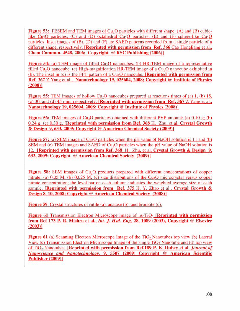
108
Figure 53: FESEM and TEM images of Cu2O particles with different shape. (A) and (B) cubic-like Cu2O particles; (C) and (D) octahedral Cu2O particles; (E) and (F) sphere-like Cu2O particles. Inset images of (B), (D) and (F) are SAED patterns recorded from a single particle of a different shape, respectively. [Reprinted with permission from Ref. 366 Cao Hongliang et al., Chem Commun. 4548, 2006; Copyright @ RSC Publishing (2006)]
Figure 54: (a) TEM image of filled Cu2O nanocubes. (b) HR-TEM image of a representative filled Cu2O nanocube. (c) High-magnification HR-TEM image of a Cu2O nanocube exhibited in (b). The inset in (c) is the FFT pattern of a Cu2O nanocube. [Reprinted with permission from
Ref. 367 Z Yang et al., Nanotechnology 19, 025604, 2008; Copyright @ Institute of Physics
(2008)] Figure 55: TEM images of hollow Cu2O nanocubes prepared at reactions times of (a) 1, (b) 15, (c) 30, and (d) 45 min, respectively. [Reprinted with permission from Ref. 367 Z Yang et al., Nanotechnology 19, 025604, 2008; Copyright @ Institute of Physics (2008)]
Figure 56: TEM images of Cu2O particles obtained with different PVP amount: (a) 0.10 g; (b) 0.24 g; (c) 0.30 g. [Reprinted with permission from Ref. 368 H. Zhu, et al. Crystal Growth
& Design 9, 633, 2009; Copyright @ American Chemical Society (2009)]
Figure 57: (a) SEM image of Cu2O particles when the pH value of NaOH solution is 11 and (b) SEM and (c) TEM images and SAED of Cu2O particles when the pH value of NaOH solution is 12. [Reprinted with permission from Ref. 368 H. Zhu, et al. Crystal Growth & Design 9,
633, 2009; Copyright @ American Chemical Society (2009)]
Figure 58: SEM images of Cu2O products prepared with different concentrations of copper nitrate: (a) 0.05 M, (b) 0.025 M, (c) size distributions of the Cu2O microcrystal versus copper nitrate concentration; the level bar on each column indicates the weighted average size of each sample. [Reprinted with permission from Ref. 375 H. Y. Zhao et al., Crystal Growth &
Design 8, 10, 2008; Copyright @ American Chemical Society (2008)]
Figure 59. Crystal structures of rutile (a), anatase (b), and brookite (c). Figure 60 Transmission Electron Microscope image of ns-TiO2 [Reprinted with permission
from Ref 173 P. R. Mishra et al., Int. J. Hyd. Eng, 28, 1089 (2003), Copyright @ Elsevier
(2003)]
Figure 61 (a) Scanning Electron Microscope Image of the TiO2 Nanotubes top view (b) Lateral View (c) Transmission Electron Microscope Image of the single TiO2 Nanotube and (d) top view of TiO2 Nanotubes. [Reprinted with permission from Ref.189 P. K. Dubey et al. Journal of
Nanoscience and Nanotechnology, 9, 5507 (2009) Copyright @ American Scientific
Publisher (2009)]

109
Figure 62 : Hydrogen generation through water photolysis using solar energy and Titanium Dioxide Photoelectrode. [Reprinted with permission from A. Fujishima et al., Functionality
of Molecular Systems, 2, 196 (1999),Copyright @ Springer 1999] Figure 63 : Schematics of Dye Sensitized Solar Cell Reprinted with permission from Michael
Grätzel, NATURE, 414,338 (2001), [Copyright @ Nature Publishing Group (2001)]
Figure 64 Schematic diagram of the fabricated photocatalytic reactor. [Reprinted with
permission from Ref.210 P. R. Mishra et al., Bull. Mater. Sci., 31, 545 (2008), Copyright @
Indian Academy of Sciences (2008)]
Figure 65 Variation of concentration of phenol with irradiation time using as synthesized nanostructured TiO2 and commercial TiO2 (P-25, Degussa) photocatalyst. (The excitation wavelength is ~ 269 nm). [Reprinted with permission from Ref.210 P. R. Mishra et al., Bull.
Mater. Sci., 31, 545 (2008), Copyright @ Indian Academy of Sciences (2008)]
Figure 66 : Tubular photocatalytic reactor for water purification [Reprinted with permission
from Ref 208 L. Zhang et al., Separation and Purification Technology, 31, 105
(2003).Copyright @ ELSEVIER (2003)]
Figure 67: Dives in Misericordia Church, Rome, Italy. (The active photocatalytic principle) Figure 68: (a) Ordinary mirror (b)TiO2 nanoparticle coated anti-fogging mirror Reprinted with
permission from K. Hashimoto et al., Japanese Journal of Applied Physics, 44, 8269
(2005),© 2005 The Japan Society of Applied Physics.
Figure 69: Animal test of photocatalytic cancer therapy; photograph of nude mouse just after initial treatment (A) and 4 weeks after treatment (B) [Reprinted with permission from A.
Fujishima, BKC, Tokyo, 1999, Copyright @ BKC (1999)]
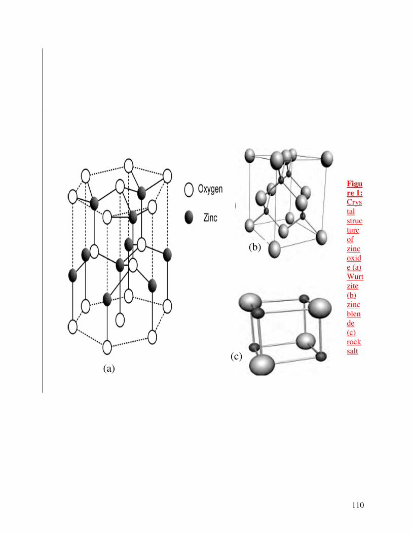
110
Figu
re 1:
Crystal structure of zinc oxide (a) Wurtzite (b) zinc blende (c) rock salt
(a)
(b)
(c)

111
Figure.2: SEM images of zinc oxide nanostructures synthesized by precipitation method at (a) 60° (b) 70° and (c) 80° C temperatures [Reprinted with permission from Ref. 208 Guzman et al., Matter. Chem. Phys. 115, 172, 2009; Copyright @ Elsevier (2009)]

112
Figure 3: SEM micrographs of mesoporous crystalline zinc oxide nanowires (a) in the PPA template and (b) released from PPA template.[Reprinted with permission from Ref. 209 Xiao
et al. Nanotech. 16, 671, 2005; Copyright @ Institute of Physics (2009)]

113
Figure 4: SEM images of zinc oxide nanostructures produced with precipitation method with (a) the control sample having large prisms and small needles (b) sample precipitated with 120 mg/L of EO68-b-MAA8-C12, and (d) the schematic view for dumbbell shape. [Reprinted with
permission from Ref. 212 Taubert et al., J. Phys. Chem. B, 107, 2660, 2003 Copyright @
American Chemical Society (2003)]

114
Figure 5: SEM images of hydrothermally synthesized zinc oxide nanomaterials (A) Nanowires [B] Nanorods [Reprinted with permission from Ref. 215 Li et al. Inorganic Chem. 42, 8105,
2003. Copyright @ American Chemical Society]
(a) (b)
(c) (d)
(e) (f)
(g) (h)
115
Figure 6: SEM images of hydrothermally synthesized zinc oxide powders using 1M aqueous solution of (a) NH4OH (b) mono (c) di- and (d) tri-ethanolamine (e) 0.2M NH4OH + 1M diethanolamine (DEA) (f) 0.4M NH4OH + 1M DEA (g) 0.6M NH4OH + 1M DEA (h) 0.2M NH4OH + 1M DEA [Reprinted with permission from Ref. 219 Lu et al., J. Alloy and
Compounds, 477, 523, 2009. Copyright @ Elsevier ]
(a) (b)
(c) (d)
(e) (f)
(g)

116
Figure 7: SEM images of hydrothermally prepared zinc oxide nanopowders at 200°C for 2h using (a) 0.25 (b) 0.5 (c) 1.0 (d) 2.0 M solution of KOH and (e) 0.025 (f) 0.05 (g) 0.20 M solution of NH3.H2O as solvent. [Reprinted with permission from Ref. 219 Xu et al., Ceramic
International, 30, 93, 2004. Copyright @ Elsevier ]
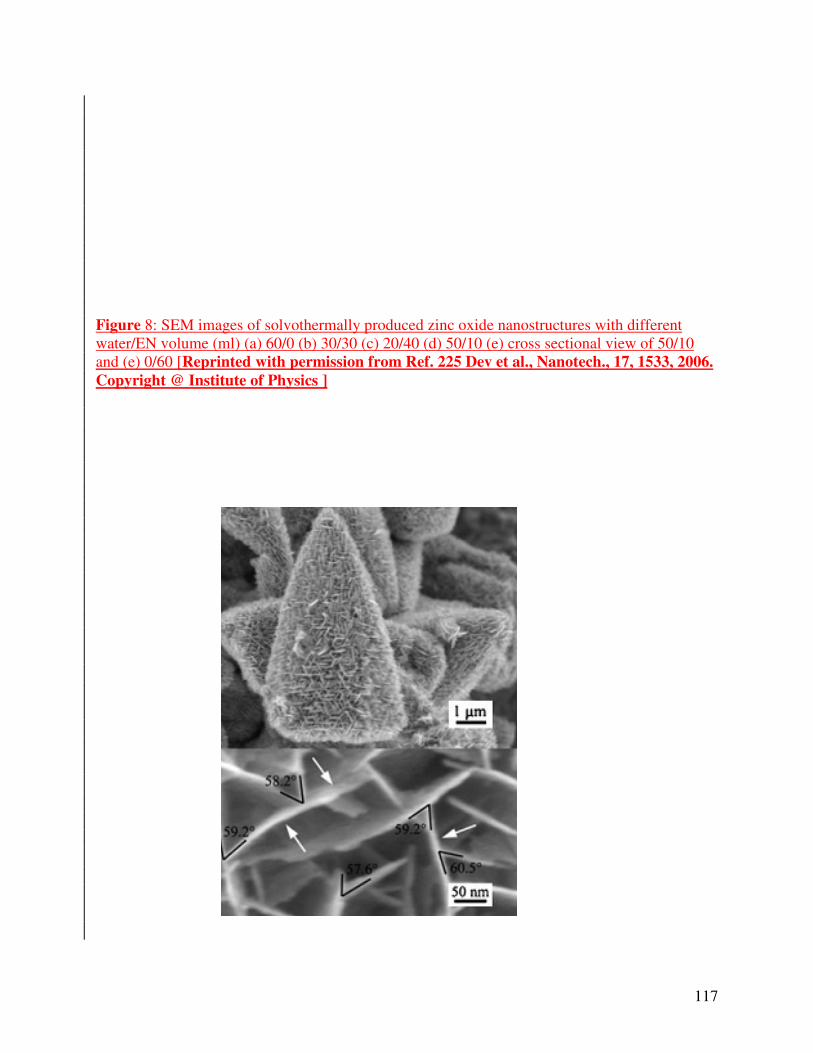
117
Figure 8: SEM images of solvothermally produced zinc oxide nanostructures with different water/EN volume (ml) (a) 60/0 (b) 30/30 (c) 20/40 (d) 50/10 (e) cross sectional view of 50/10 and (e) 0/60 [Reprinted with permission from Ref. 225 Dev et al., Nanotech., 17, 1533, 2006.
Copyright @ Institute of Physics ]
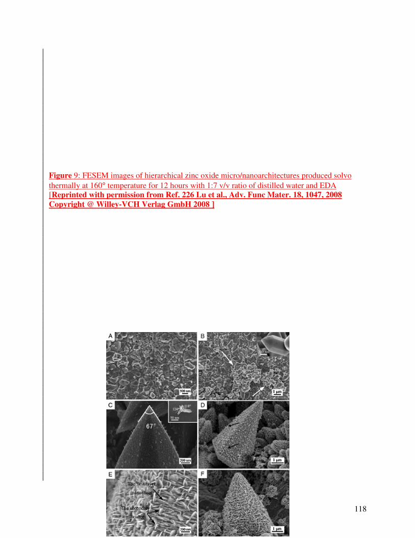
118
Figure 9: FESEM images of hierarchical zinc oxide micro/nanoarchitectures produced solvo thermally at 160° temperature for 12 hours with 1:7 v/v ratio of distilled water and EDA [Reprinted with permission from Ref. 226 Lu et al., Adv. Func Mater. 18, 1047, 2008
Copyright @ Willey-VCH Verlag GmbH 2008 ]
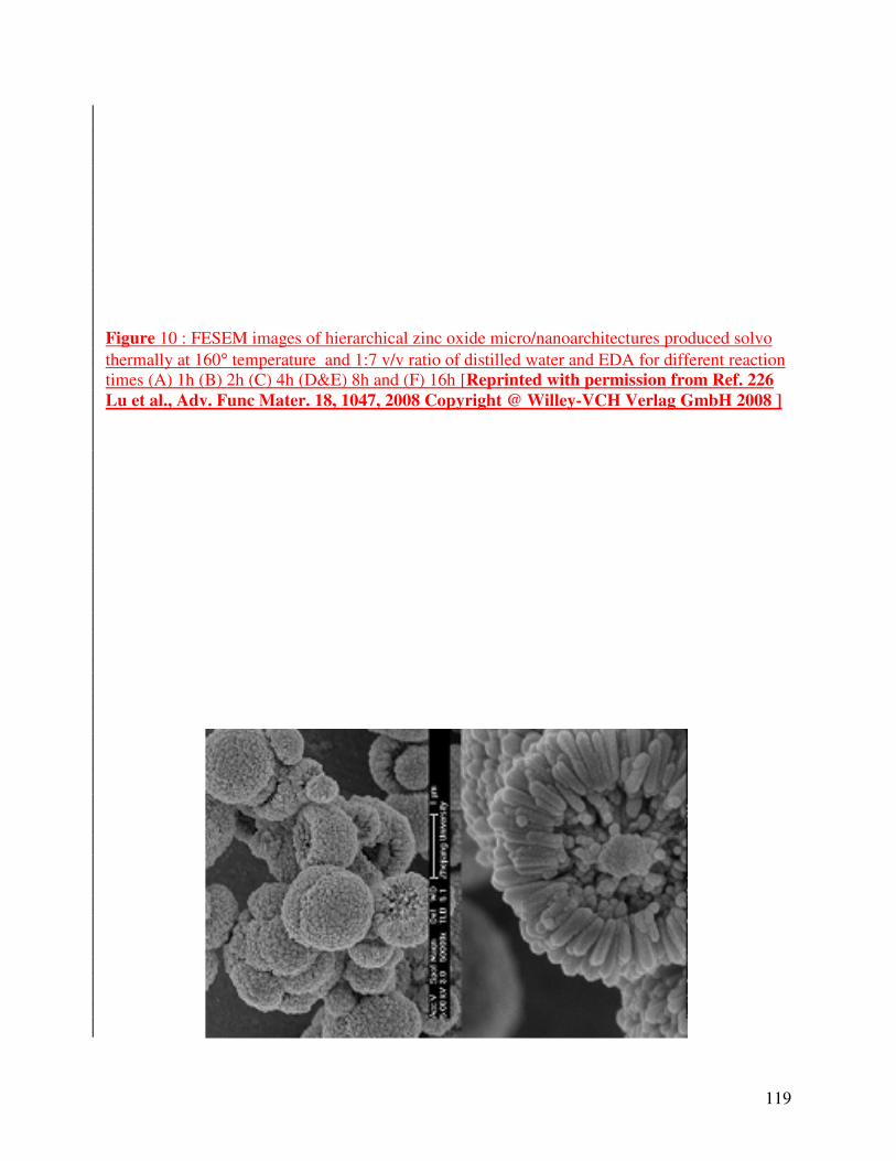
119
Figure 10 : FESEM images of hierarchical zinc oxide micro/nanoarchitectures produced solvo thermally at 160° temperature and 1:7 v/v ratio of distilled water and EDA for different reaction times (A) 1h (B) 2h (C) 4h (D&E) 8h and (F) 16h [Reprinted with permission from Ref. 226
Lu et al., Adv. Func Mater. 18, 1047, 2008 Copyright @ Willey-VCH Verlag GmbH 2008 ]

120
Figure 11: SEM images of 3D zinc oxide hollow micro-sphere synthesized by the solvothermal method in the EG solution at 200 °C temperature, general view in the left, at high magnification at right Fig. 2.10 A: FESEM images of hierarchical zinc oxide micro/nanoarchitectures produced solvo thermally at 160° temperature for 12 hours with 1:7 v/v ratio of distilled water and EDA [Reprinted with permission from Ref. 227 Zhang et al., Nanotech. 18, 455604,
2007 Copyright @ Institute of Physics 2007 ]
(a) (b) (c) (d)
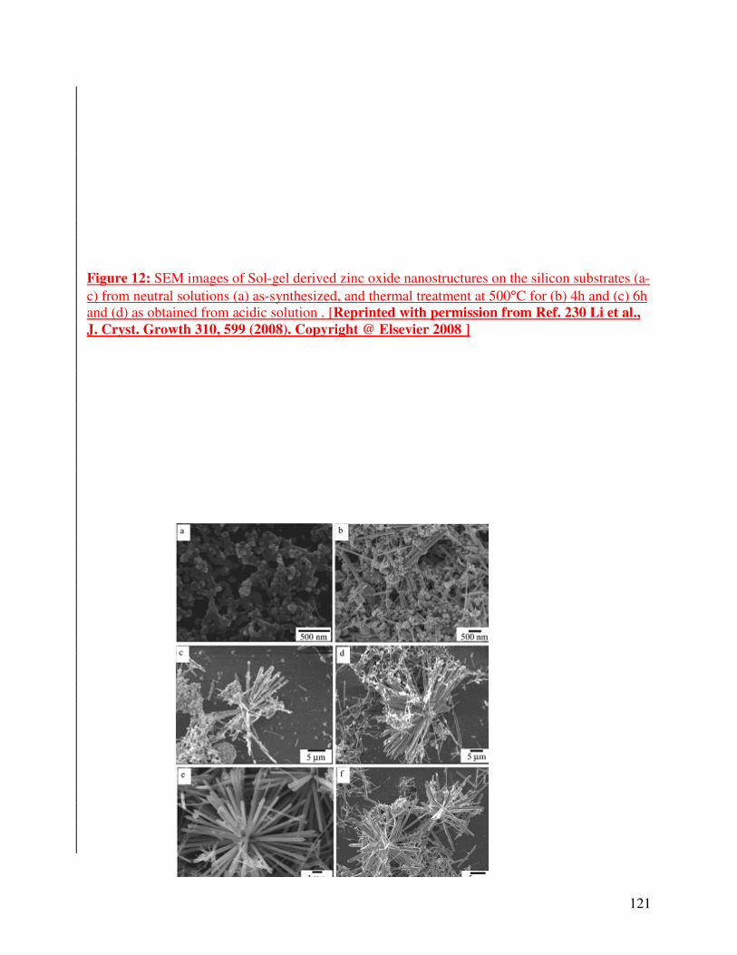
121
Figure 12: SEM images of Sol-gel derived zinc oxide nanostructures on the silicon substrates (a-c) from neutral solutions (a) as-synthesized, and thermal treatment at 500°C for (b) 4h and (c) 6h and (d) as obtained from acidic solution . [Reprinted with permission from Ref. 230 Li et al.,
J. Cryst. Growth 310, 599 (2008). Copyright @ Elsevier 2008 ]

122
Figure 13: SEM images of one dimensional micro-emulsion derived zinc oxide nanostructures obtained after different reaction times (a) 10 min, (b) 30 min, (c) 1h (d) 2h (e) 4h and (f) 8 h. [Reprinted with permission from Ref. 232 Zhang et al., Cryst. Growth Design 4, 309,2004.
Copyright @ American Chemical Society 2004 ]

123
Figure 14: SEM images of zinc oxide nanostructures obtained by combustion synthesis method using (a) calcination of 0.2g Zn(NO3).6H2O for 2h at 800°C (b) By combustion and (c) by solution combustion (d) solution combustion with 1.0 ml of additional water. [Reprinted with
permission from Ref. 238 Alvarado-Ibarra et al., Colloid Surf. A: Physiochem. Eng.
Aspects, 345, 135, 2009. Copyright @ Elsevier 2008]

124
Figure 15: SEM image of melting combustion synthesized zinc oxide nanostructure. [Reprinted
with permission from Ref. 239 Chen et al., Matter Lett. 61, 4603, 2007 Copyright @
Elsevier 2008]

125
Figure 16: SEM images of the Eelctrochemically obtained zinc oxide films prepared at the cathode potential ranging from -0.7 to -1.4V vs Ag/AgCl [Reprinted with permission from
Ref. 243 Izaki and Omi, Appl. Phys. Lett., 68, 2439, 1996. Copyright @ American Institute
of Physics 1996]
Figu
re
17: SEM images of electrochemically synt
hesized
ZnO nanostruc
(a) (b) (c)
(d) (e) (f)

126
tures in the electrolytic solution of (a) 0.5M ZnCl2+0.02 M citric acid (b) 0.5M ZnCl2+0.01 M citric acid (c) 0.5M ZnCl2+0.05 M citric acid (d) 0.5M ZnCl2+0.0001 M citric acid (e) 0.25 M +0.01M citric acid (f) 0.25M ZnCl2+0.01 M citric acid+0.1MKCl [Reprinted with permission
from Ref. 260 Li et al., J. Phys. Chem. C, 111, 6678, 2007. Copyright @ American
Chemical Society 2007]

127
Figure 18: SEM images of (a) primary ZnO nanosheets and (b-d) hierarchical ZnO nanorods on hexagonal nanosheets on ITO substrates. [Reprinted with permission from Ref. 261 Xu et al.,
J. Phys. Chem. C, 111, 11560, 2007. Copyright @ American Chemical Society 2007]
Figure 19: SEM
images of
hierarchical ZnO nanostructures electrodeposited at a potential of -1.10 V in 0.05M [Zn(NH3)4-2
solution for different deposition times (a) 10min, (b) 20min, (c) 40min, (d) 1.5h, (e) 2.5h, (f)3.5h [Reprinted with permission from Ref. 261 Xu et al., J. Phys. Chem. C, 111, 11560, 2007.
Copyright @ American Chemical Society 2007]
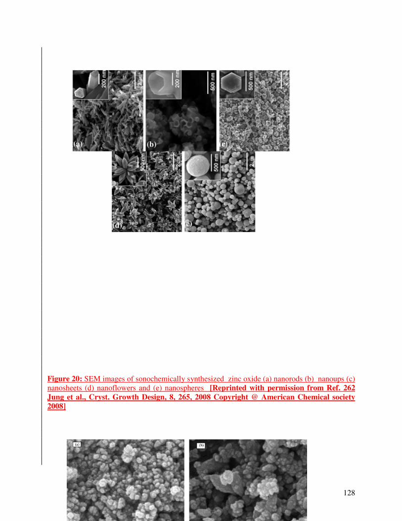
128
Figure 20: SEM images of sonochemically synthesized zinc oxide (a) nanorods (b) nanoups (c) nanosheets (d) nanoflowers and (e) nanospheres [Reprinted with permission from Ref. 262
Jung et al., Cryst. Growth Design, 8, 265, 2008 Copyright @ American Chemical society
2008]
(a) (b) (c)
(d) (e)

129
Fig. 21: SEM images of the ZnO samples prepared by sonochemical method using the mixture of Zn(NO3)2 and NaOH as precursor at different pH value:(a) pH 9.5 (b) pH 10.5(c) pH 11.5 and (d) pH 12.5. [Reprinted with permission from Ref. 266 Xiao et al., J. Alloy and Comp. 459,
L18, 2008 Copyright @ Elsevier 2008]

130
Figure 22: SEM images of as-made ZnO powders prepared by sonochemical method using the mixture of different zincs salt and NaOH as precursor at pH 12.5 (a)Zn(NO3)2 (b)ZnCl2 (c)ZnSO4 and (d) Zn(C2H4O2)2 .[Reprinted with permission from Ref. 266 Xiao et al., J.
Alloy and Comp. 459, L18, 2008 Copyright @ Elsevier 2008]

131
Figure 23[A]: FESEM images of cyclic feeding chemical vapor deposited zinc oxide flower shaped zinc oxide nanostructures on Si (a,b) 100 and (c,d) 111 substrates. [Reprinted with
permission from Ref. 273 Umar et al., Nanotech. 16, 2462, 2005 Copyright @ Institute of
Physics 2005]
(a) (b)
(c) (d)
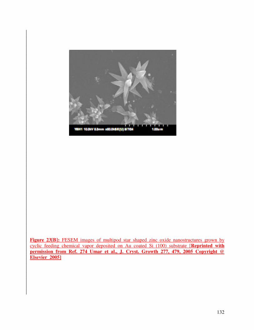
132
Figure 23[B]: FESEM images of multipod star shaped zinc oxide nanostructures grown by cyclic feeding chemical vapor deposited on Au coated Si (100) substrate [Reprinted with
permission from Ref. 274 Umar et al., J. Cryst. Growth 277, 479, 2005 Copyright @
Elsevier 2005]
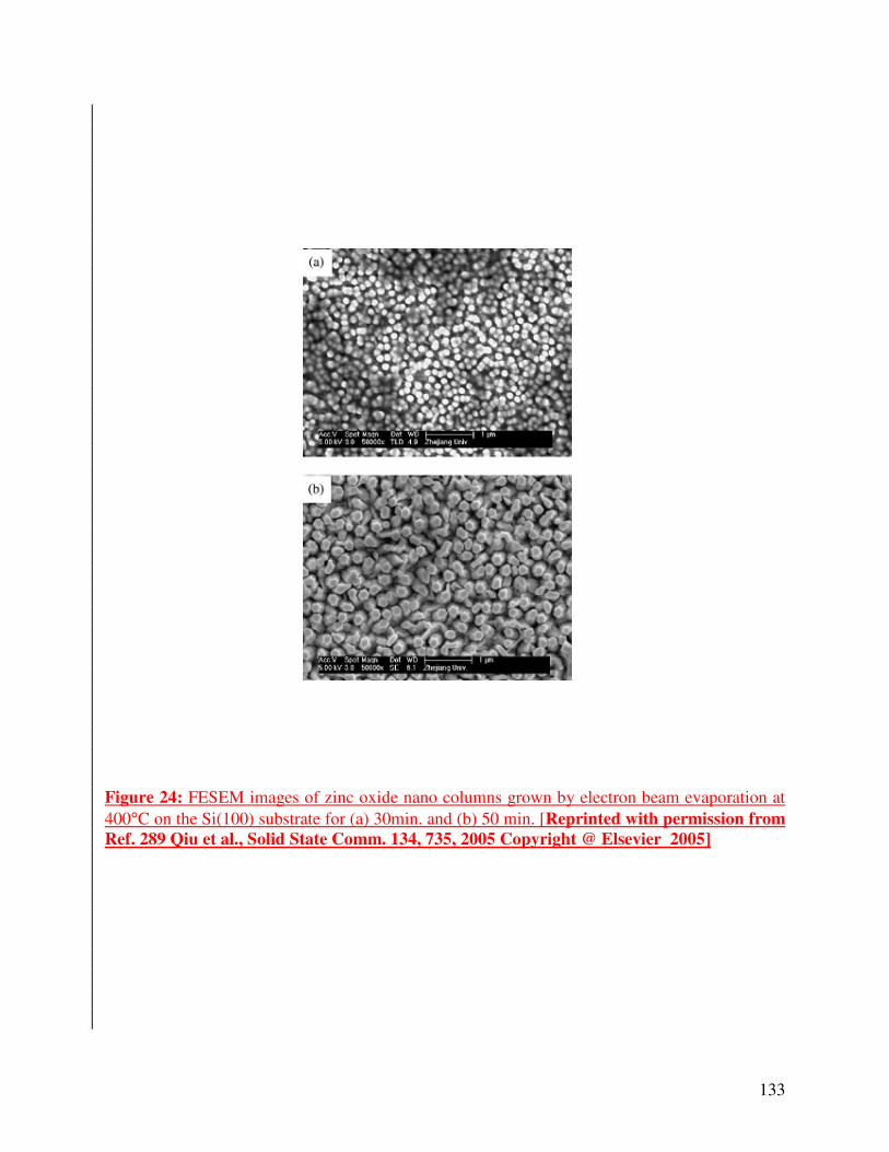
133
Figure 24: FESEM images of zinc oxide nano columns grown by electron beam evaporation at 400°C on the Si(100) substrate for (a) 30min. and (b) 50 min. [Reprinted with permission from
Ref. 289 Qiu et al., Solid State Comm. 134, 735, 2005 Copyright @ Elsevier 2005]
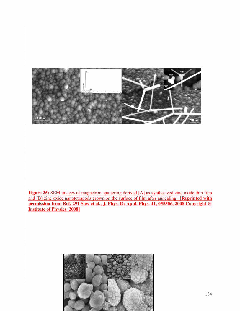
134
Figure 25: SEM images of magnetron sputtering derived [A] as synthesized zinc oxide thin film and [B] zinc oxide nanotetrapods grown on the surface of film after annealing . [Reprinted with
permission from Ref. 291 Saw et al., J. Phys. D: Appl. Phys. 41, 055506, 2008 Copyright @
Institute of Physics 2008]

135
Figure 26: SEM images of zinc oxide nanostructures grown by RF sputtering for (a) 15 min. and (b) 50 min. [Reprinted with permission from Ref. 294 Youn et al., Jap. J. Appl. Phys.
45, 8957, 2006 Copyright @ Japanese J. Appl. Phys., 2006]

136
Figure 27 : X-ray diffraction patterns of vacuum arc deposited zinc oxide thin films at (a) low (b) high magnetic fields [Reprinted with permission from Ref. 296 Takikawa et al., Thin
Solid Films 377, 74 , 2000 Copyright @ Elsevier 2006]

137
Figure 28: SEM images of Spray Pyrolysis deposited zinc oxide nanostructures on ITO/glass substrate using 0.1mol/lit. solution of zinc chloride at different (a) 400°C (b) 450°C (c) 490°C (d) 540°C and (e) 560°C substrate temperatures [Reprinted with permission from Ref. 314
Krunks et al., Thin Solid Films 515, 1157 , 2006 Copyright @ Elsevier 2006]

138
Figure 29: (a) Emission spectra from N doped zinc oxide nanoneedle under different pumping powers (b) Output power vs pump energy curve [Reprinted with permission from Ref. 319,
Tanemura et al., Surf. Sci., 601, 4459, 2007 Copyright @ Elsevier 2007]
D
E
(a) (d)
(c)
(b)
(e)
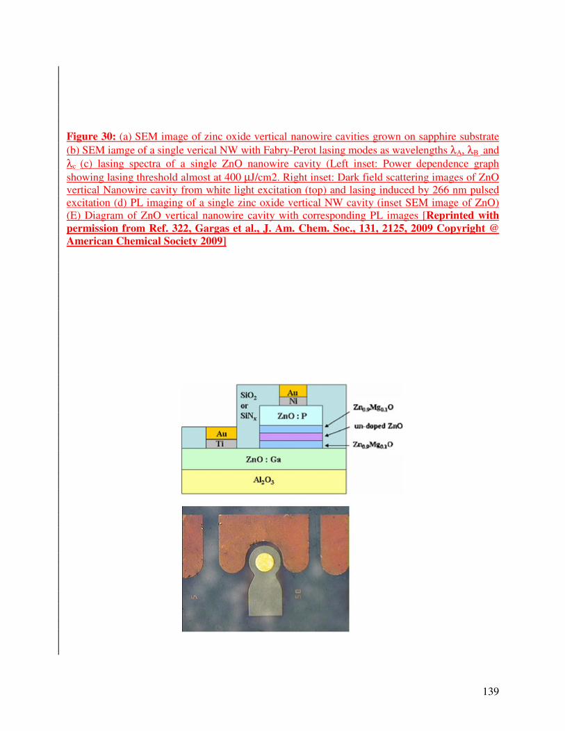
139
Figure 30: (a) SEM image of zinc oxide vertical nanowire cavities grown on sapphire substrate (b) SEM iamge of a single verical NW with Fabry-Perot lasing modes as wavelengths λA, λB and λc (c) lasing spectra of a single ZnO nanowire cavity (Left inset: Power dependence graph showing lasing threshold almost at 400 µJ/cm2. Right inset: Dark field scattering images of ZnO vertical Nanowire cavity from white light excitation (top) and lasing induced by 266 nm pulsed excitation (d) PL imaging of a single zinc oxide vertical NW cavity (inset SEM image of ZnO) (E) Diagram of ZnO vertical nanowire cavity with corresponding PL images [Reprinted with
permission from Ref. 322, Gargas et al., J. Am. Chem. Soc., 131, 2125, 2009 Copyright @
American Chemical Society 2009]

140
Figure 31: (Top) Schematic view of zinc oxide based hetrojunction p-n LED (Bottom) Optical microscope plan view of a zinc oxide based hetrojunction LED. [Reprinted with permission
from Ref. 53, Wang et al., Appl. Phys. Lett., 92, 112101, 2008 Copyright @ American
Institute of Physics 2008]
.
(a)
(d) (c)
(b)
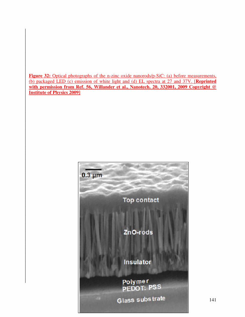
141
Figure 32: Optical photographs of the n-zinc oxide nanorods/p-SiC: (a) before measurements, (b) packaged LED (c) emission of white light and (d) EL spectra at 27 and 37V. [Reprinted
with permission from Ref. 56, Willander et al., Nanotech. 20, 332001, 2009 Copyright @
Institute of Physics 2009]

142
Figure 33: Cross sectional SEM image of a ZnO/polymer multi layer LED fabricated on glass substrate. [Reprinted with permission from Ref. 56, Willander et al., Nanotech. 20, 332001,
2009 Copyright @ Institute of Physics 2009]
(a) (b)

143
Figure 34: (Top) Current density-voltage characteristic of (a) NPD-PFO structure and (b) PVK-TFB structure (inset shows a schematic diagram of the corresponding energy band energy band diagram) and (Bottom) Coressponding EL spectra at 14V and 0.10mA [Reprinted with
permission from Ref. 56, Willander et al., Nanotech. 20, 332001, 2009 Copyright @
Institute of Physics 2009]
Figure 35: (a) Cu2O deposited at pH 9 (0.05 mA/cm2; 0.1 C/cm2; 55°C). (b) Cu2O deposited at pH 9 (0.05 mA/cm2; 0.1 /cm2; 10°C). (c) Cu2O deposited at pH 11 (0.2 mA/cm2; 0.13 C/cm2; 55°C). [Reprinted with permission from Ref. 333 P. E. d. Jongh et al., Chem.
Mater. 11, 3512, 1999; Copyright @ American Chemical Society (1999)]

144
Figure 36: (a) Scanning electron micrograph of electrodeposited Cu2O nanowires. Bath temperature = 70 0C, pH =9.1, E =-1:69V/SSE. (b) Enlarged of (a). [Reprinted with
permission from Ref. 337 A. L. Daltin et al., Journal of Crystal Growth 282, 414,
2005; Copyright @ Elsevier (2005)]
(a) (b)
Figure 37: Typical FE-SEM images of octahedral Cu2O located at the ITO substrate at different magnifications (the deposition time is 15 min; the concentration of Cu(OH)4
2- is 25 mM). [Reprinted
with permission from Ref. 341 S. Guo et al., Inorganic Chemistry
46, 9537, 2007; Copyright @
American Chemical Society
(2007)]

145
Figure 39: (a-d) SEM micrographs of the copper electrode after electrolysis at different voltage (2, 4, 8, and 10 V, respectively). [Reprinted with permission from Ref. 342 D. P. Singh et al., J.
Phys. Chem. C 111, 1638, 2007; Copyright @ American Chemical Society (2007)]
a b
(c) (d)
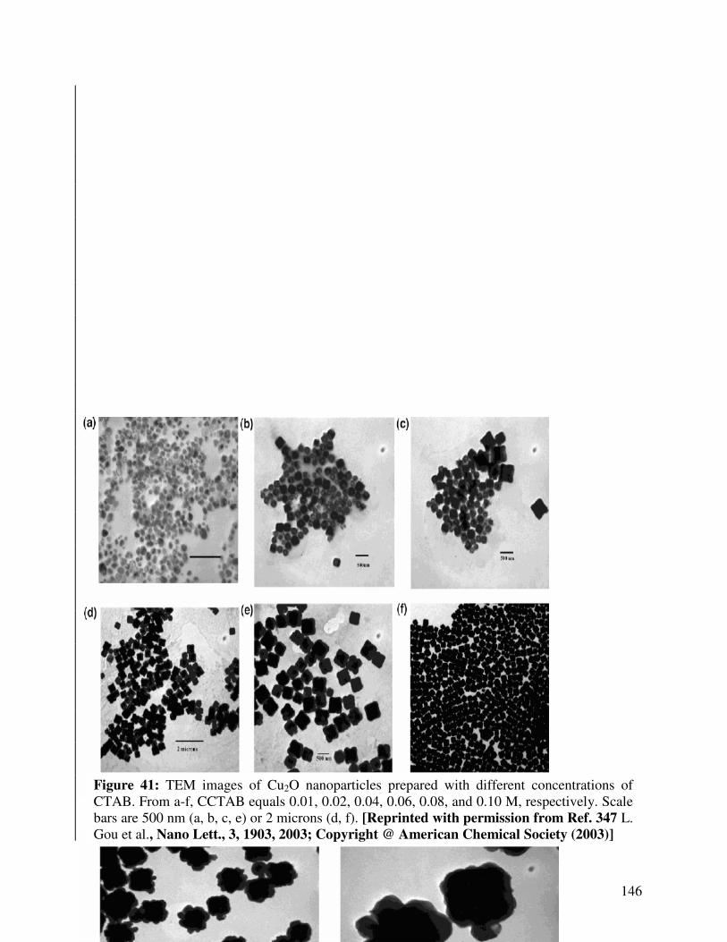
146
Figure 41: TEM images of Cu2O nanoparticles prepared with different concentrations of CTAB. From a-f, CCTAB equals 0.01, 0.02, 0.04, 0.06, 0.08, and 0.10 M, respectively. Scale bars are 500 nm (a, b, c, e) or 2 microns (d, f). [Reprinted with permission from Ref. 347 L. Gou et al., Nano Lett., 3, 1903, 2003; Copyright @ American Chemical Society (2003)]

147
(g)
(h)
(i)
(j)
(k)
(l)
(m)
(n)
(o)
(p)
(q)
Figure 43: a: TEM micrograph (scale bar~100 nm) and histogramof the size distribution fromsample B2; b: TEMmicrograph (scale bar~100 nm) and histogram of the size distribution from sample B3; c: TEM micrograph (scale bar ~ 100 nm) and histogram of the size distribution from sample B4. [Reprinted with permission from Ref. 349 L. Gou et al., J.
Mater. Chem. 14, 735, 2004; Copyright @ RSC publishing (2004)]
(a) (c) (b)
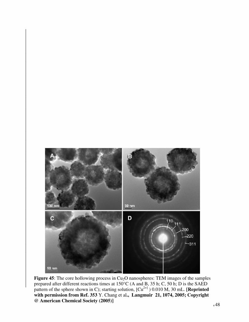
148
Figure 45: The core hollowing process in Cu2O nanospheres: TEM images of the samples prepared after different reactions times at 150°C (A and B, 35 h; C, 50 h; D is the SAED pattern of the sphere shown in C); starting solution, [Cu2+] ) 0.010 M, 30 mL. [Reprinted
with permission from Ref. 353 Y. Chang et al., Langmuir 21, 1074, 2005; Copyright
@ American Chemical Society (2005)]
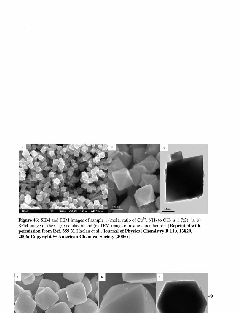
149
Figure 46: SEM and TEM images of sample 1 (molar ratio of Cu2+, NH3 to OH- is 1:7:2): (a, b) SEM image of the Cu2O octahedra and (c) TEM image of a single octahedron. [Reprinted with
permission from Ref. 359 X. Haolan et al., Journal of Physical Chemistry B 110, 13829,
2006; Copyright @ American Chemical Society (2006)]

150
Figure 48: TEM images of the sample after various times of oxidation: 0, 30, 90, 150, and 210 min and after an aging period of 3 days. (a) Cu nanoparticles, (b) faceted Cu2O nanocrystals, (c) hexagonal nanoplates, (d) truncated nanoprisms, (e) triangular nanoplates, and (f) octahedral nanocrystals. [Reprinted with
permission from Ref. 360 C. H. Bernard Ng et al., J. Phys.
Chem. B 110, 20801, 2006;
Copyright @ American
Chemical Society (2006)]

151
Figure 50: FE-SEM images of samples prepared with 0.02 molâL-1 CuSO4, 0.02 molâL-1 EDTA, 0.333 molâL-1 NaOH, and 0.028 molâL-1 C6H12O6 for 12 h at different reaction temperatures (w ) 34). (a) Room temperature. (b) 80 °C. [Reprinted with
permission from Ref. 362 H. Zhang et al., Crystal Growth & Design 7, 820, 2007;
Copyright @ American Chemical Society (2007)]
Figure 49: Typical FE-SEM images of the products prepared with 0.02 molâL-1 CuSO4, 0.02 molâL-1 EDTA, 0.333 molâL-1 NaOH, and 0.028 molâL-1 C6H12O6 at 60 °C for 12 h (w ) 34). (a) Low magnification image and (b) high magnification. [Reprinted with
permission from Ref. 362 H. Zhang et al., Crystal Growth & Design 7, 820, 2007;
Copyright @ American Chemical Society (2007)]

152
Figure 52: SEM micrographs of Cu2O nanowires organized as (a) spherical structures, or (b) cone-shaped bundles, (c) insert of the organization of nanowires, (d) conical structures of disassembled nanowires. [Reprinted with permission from Ref. 363 Z. C. Orel et al. Crystal
Growth & Design 7, 453, 2007; Copyright @ American Chemical Society (2007)]
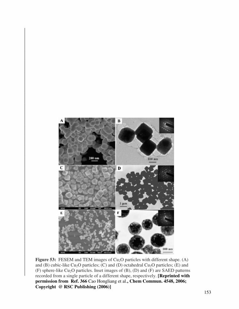
153
Figure 53: FESEM and TEM images of Cu2O particles with different shape. (A) and (B) cubic-like Cu2O particles; (C) and (D) octahedral Cu2O particles; (E) and (F) sphere-like Cu2O particles. Inset images of (B), (D) and (F) are SAED patterns recorded from a single particle of a different shape, respectively. [Reprinted with
permission from Ref. 366 Cao Hongliang et al., Chem Commun. 4548, 2006;
Copyright @ RSC Publishing (2006)]
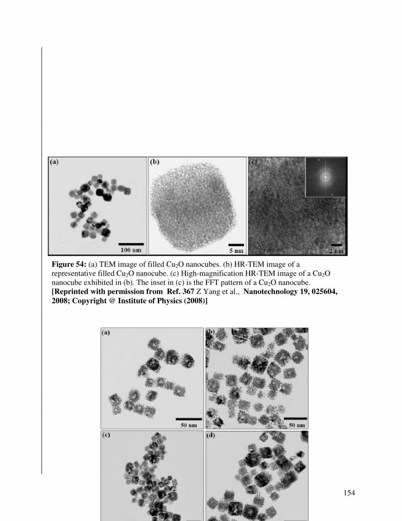
154
Figure 54: (a) TEM image of filled Cu2O nanocubes. (b) HR-TEM image of a representative filled Cu2O nanocube. (c) High-magnification HR-TEM image of a Cu2O nanocube exhibited in (b). The inset in (c) is the FFT pattern of a Cu2O nanocube. [Reprinted with permission from Ref. 367 Z Yang et al., Nanotechnology 19, 025604,
2008; Copyright @ Institute of Physics (2008)]
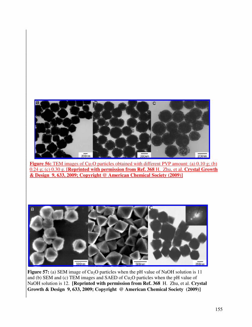
155
Figure 56: TEM images of Cu2O particles obtained with different PVP amount: (a) 0.10 g; (b) 0.24 g; (c) 0.30 g. [Reprinted with permission from Ref. 368 H. Zhu, et al. Crystal Growth
& Design 9, 633, 2009; Copyright @ American Chemical Society (2009)]
Figure 57: (a) SEM image of Cu2O particles when the pH value of NaOH solution is 11 and (b) SEM and (c) TEM images and SAED of Cu2O particles when the pH value of NaOH solution is 12. [Reprinted with permission from Ref. 368 H. Zhu, et al. Crystal
Growth & Design 9, 633, 2009; Copyright @ American Chemical Society (2009)]
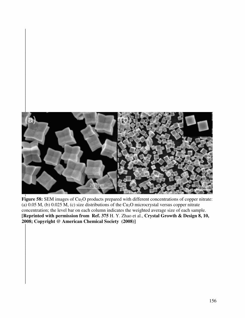
156
Figure 58: SEM images of Cu2O products prepared with different concentrations of copper nitrate: (a) 0.05 M, (b) 0.025 M, (c) size distributions of the Cu2O microcrystal versus copper nitrate concentration; the level bar on each column indicates the weighted average size of each sample. [Reprinted with permission from Ref. 375 H. Y. Zhao et al., Crystal Growth & Design 8, 10,
2008; Copyright @ American Chemical Society (2008)]

157
Figure 59. Crystal structures of rutile (a), anatase (b), and brookite (c).
(a) (b) (c)

158
Figure 60 Transmission Electron Microscope image of ns-TiO2 [Reprinted with permission
from Ref 173 P. R. Mishra et al., Int. J. Hyd. Eng, 28, 1089 (2003), Copyright @ Elsevier
(2003)]

159
Figu
re 61 (a)
Scanning
Electron
Microsco
pe Image of
the TiO2
Nanotub
es top view (b) Lateral View (c) Transmission Electron Microscope Image of the single TiO2 Nanotube and (d) top view of TiO2 Nanotubes. [Reprinted with permission from Ref.189 P. K.
Dubey et al. Journal of Nanoscience and Nanotechnology, 9, 5507 (2009) Copyright @
American Scientific Publisher (2009)]
(a) (b)
(c) (d)
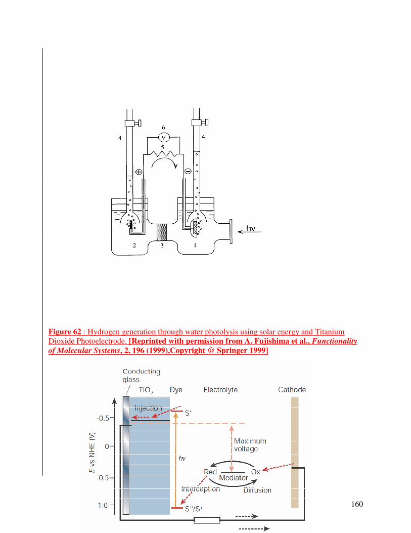
160
Figure 62 : Hydrogen generation through water photolysis using solar energy and Titanium Dioxide Photoelectrode. [Reprinted with permission from A. Fujishima et al., Functionality
of Molecular Systems, 2, 196 (1999),Copyright @ Springer 1999]

161
Figure 63 : Schematics of Dye Sensitized Solar Cell Reprinted with permission from Michael
Grätzel, NATURE, 414,338 (2001), [Copyright @ Nature Publishing Group (2001)]
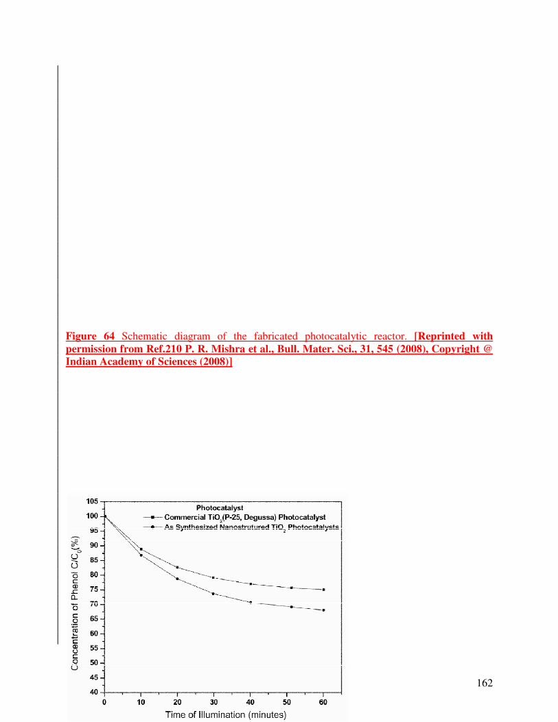
162
Figure 64 Schematic diagram of the fabricated photocatalytic reactor. [Reprinted with
permission from Ref.210 P. R. Mishra et al., Bull. Mater. Sci., 31, 545 (2008), Copyright @
Indian Academy of Sciences (2008)]
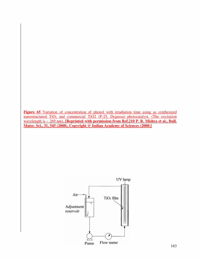
163
Figure 65 Variation of concentration of phenol with irradiation time using as synthesized nanostructured TiO2 and commercial TiO2 (P-25, Degussa) photocatalyst. (The excitation wavelength is ~ 269 nm). [Reprinted with permission from Ref.210 P. R. Mishra et al., Bull.
Mater. Sci., 31, 545 (2008), Copyright @ Indian Academy of Sciences (2008)]

164
Figure 66 : Tubular photocatalytic reactor for water purification [Reprinted with permission
from Ref 208 L. Zhang et al., Separation and Purification Technology, 31, 105
(2003).Copyright @ ELSEVIER (2003)]

165
Figure 67: Dives in Misericordia Church, Rome, Italy. (The active photocatalytic principle)
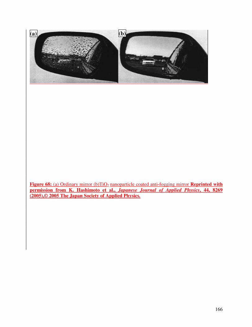
166
Figure 68: (a) Ordinary mirror (b)TiO2 nanoparticle coated anti-fogging mirror Reprinted with
permission from K. Hashimoto et al., Japanese Journal of Applied Physics, 44, 8269
(2005),© 2005 The Japan Society of Applied Physics.
(a) (b)

167
Figure 69: Animal test of photocatalytic cancer therapy; photograph of nude mouse just after initial treatment (A) and 4 weeks after treatment (B) [Reprinted with permission from A.
Fujishima, BKC, Tokyo, 1999, Copyright @ BKC (1999)]
Related Documents